PSoC® 6 MCU: PSoC 62
Datasheet
®
PRELIMINARY
Programmable System-on-Chip (PSoC )
General Description
PSoC® is a scalable and reconfigurable platform architecture for a family of programmable embedded system controllers with ARM®
Cortex™ CPUs (single and multi-core). The PSoC 6 product family, based on an ultra low-power 40-nm platform, is a combination of
a dual-core microcontroller with low-power Flash technology and digital programmable logic, high-performance analog-to-digital and
digital-to-analog conversion, low-power comparators, and standard communication and timing peripherals.
Features
32-bit Dual Core CPU Subsystem
Flexible Clocking Options
■
150-MHz ARM Cortex-M4F CPU with single-cycle multiply
(Floating Point and Memory Protection Unit)
■
On-chip crystal oscillators (High-speed, 4 to 33 MHz, and
Watch crystal, 32 kHz)
■
100-MHz Cortex M0+ CPU
■
Phase-locked Loop (PLL) for multiplying clock frequencies
■
User-selectable core logic operation at either 1.1 V or 0.9 V
■
8 MHz Internal Main Oscillator (IMO) with 1% accuracy
■
Inter-processor communication supported in hardware
■
■
8 KB 4-way set-associative Instruction Caches for the M4 and
M0+ CPUs respectively
Ultra low-power 32-kHz Internal Low-speed Oscillator (ILO)
with 10% accuracy
■
IMO can be locked to 32 kHz WCO input for better accuracy
■
Frequency Locked Loop (FLL) for multiplying IMO frequency
■
■
■
Active CPU power consumption slope with 1.1-V core operation
for the Cortex M4 is 40 µA/MHz and 20 µA/MHz for the Cortex
M0+, both at 3.3-V chip supply voltage with the internal buck
regulator
Active CPU power consumption slope with 0.9-V core operation
for the Cortex M4 is 22 µA/MHz and 15 µA/MHz for the Cortex
M0+, both at 3.3-V chip supply voltage with the internal buck
regulator
Two DMA controllers with 16 channels each
Serial Communication
■
Nine independent run-time reconfigurable serial communication blocks (SCBs), each is software configurable as I2C,
SPI, or UART
■
USB Full-Speed Dual-role Host and Device interface
Timing and Pulse-Width Modulation
■
Thirty-two 16-bit
(TCPWM) blocks
■
Center-aligned, Edge, and Pseudo-random modes
■
Comparator-based triggering of Kill signals
Flexible Memory Sub-system
■
1 MB Application Flash with 32-KB EEPROM area and 32-KB
Secure Flash
■
128-bit wide Flash accesses reduce power
■
Flash Read-While-Write (RWW) allows updating the Flash
while executing from it
Drive modes, strengths, and slew rates are programmable
Six overvoltage tolerant (OVT) pins
SRAM with Selectable Retention Granularity
■
288-KB integrated SRAM
Packages
■
32-KB retention boundaries (can retain 32K to 288K in 32K
increments)
■
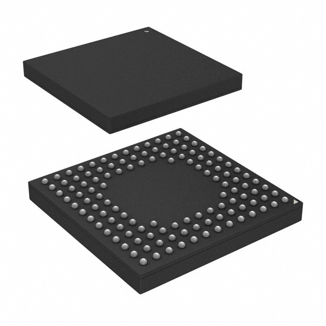
124-BGA
One-Time-Programmable (OTP) E-Fuse memory for validation
and security
■
80-WLCSP
Audio Subsystem
■
■
Active, Low-power Active, Sleep, Low-power Sleep, Deep
Sleep, and Hibernate modes for fine-grained power
management
Deep Sleep mode current with 64K SRAM retention is 7 µA
with 3.3 V external supply and internal buck
■
On-chip Single-In Multiple Out (SIMO) DC-DC Buck converter,
很抱歉,暂时无法提供与“CY8C6246BZI-D04”相匹配的价格&库存,您可以联系我们找货
免费人工找货