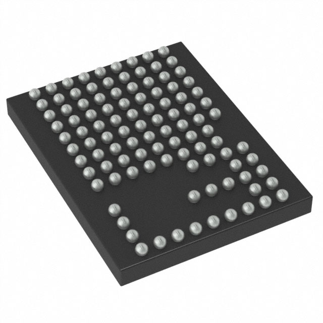
PSoC® 6 MCU: PSoC 63 with BLE
Datasheet
®
Programmable System-on-Chip (PSoC )
General Description
PSoC® is a scalable and reconfigurable platform architecture for a family of programmable embedded system controllers with
Arm® Cortex™ CPUs (single and multi-core). The PSoC 63 product family, based on an ultra low-power 40-nm platform, is a combination of a dual-core microcontroller with low-power Flash technology and digital programmable logic, high-performance
analog-to-digital and digital-to-analog conversion, low-power comparators, and standard communication and timing peripherals. The
PSoC 63 family provides wireless connectivity with BLE 5.0 compliance.
Features
32-bit Dual Core CPU Subsystem
Low-Power 1.7-V to 3.6-V Operation
150-MHz Arm Cortex-M4F CPU with single-cycle multiply
(Floating Point and Memory Protection Unit)
■ 100-MHz Cortex M0+ CPU with single-cycle multiply and MPU.
■ User-selectable core logic operation at either 1.1 V or 0.9 V
■ Inter-processor communication supported in hardware
■ 8 KB 4-way set-associative Instruction Caches for the M4 and
M0+ CPUs respectively
■ Active CPU power consumption slope with 1.1-V core operation
for the Cortex M4 is 40 µA/MHz and 20 µA/MHz for the Cortex
M0+, both at 3.3-V chip supply voltage with the internal buck
regulator
■ Active CPU power consumption slope with 0.9-V core operation
for the Cortex M4 is 22 µA/MHz and 15 µA/MHz for the Cortex
M0+, both at 3.3-V chip supply voltage with the internal buck
regulator
■ Two DMA controllers with 16 channels each
■
■
■
■
■
Flexible Clocking Options
■
On-chip crystal oscillators (High-speed, 4 to 33 MHz, and
Watch crystal, 32 kHz)
■
Phase Locked Loop (PLL) for multiplying clock frequencies
■
8 MHz Internal Main Oscillator (IMO) with 2% accuracy
■
Ultra low-power 32 kHz Internal Low-speed Oscillator (ILO)
with ±10% accuracy
■
Frequency Locked Loop (FLL) for multiplying IMO frequency
Flash Memory Sub-system
1 MB Application Flash with 32-KB EEPROM area and 32-KB
Secure Flash
■ 128-bit wide Flash accesses reduce power
■ SRAM with Selectable Retention Granularity
■ 288-KB integrated SRAM
■ 32-KB retention boundaries (can retain 32 KB to 288 KB in
32-KB increments)
■ One-Time-Programmable (OTP) E-Fuse memory for validation
and security
■
Bluetooth Low Energy (Bluetooth Smart) BT 5.0
Subsystem
2.4-GHz RF transceiver with 50- antenna drive
Digital PHY
■ Link Layer engine supporting master and slave modes
■ Programmable output power: up to 4 dBm
■ RX sensitivity: –95 dBm
■ RSSI: 4-dB resolution
■ 5.7 mA TX (0 dBm) and 6.7 mA RX (2 Mbps) current with 3.3-V
battery and internal SIMO Buck converter
■ Link Layer engine supports four connections simultaneously
■ Supports 2 Mbps LE data rate
■
■
Cypress Semiconductor Corporation
Document Number: 002-18787 Rev. *G
•
Active, Low-power Active, Sleep, Low-power Sleep, Deep
Sleep, and Hibernate modes for fine-grained power
management
Deep Sleep mode current with 64-KB SRAM retention is 7 µA
with 3.3-V external supply and internal buck
On-chip Single-In Multiple Out (SIMO) DC-DC Buck converter,
很抱歉,暂时无法提供与“CY8C6347FMI-BLD53T”相匹配的价格&库存,您可以联系我们找货
免费人工找货