CY8CKIT-041-41XX
PSoC® 4100S Pioneer Kit Guide
Doc. # 002-14067 Rev. *C
Cypress Semiconductor
198 Champion Court
San Jose, CA 95134-1709
Phone (USA): 800.858.1810
Phone (Intnl): +1.408.943.2600
www.cypress.com
�Copyrights
Copyrights
© Cypress Semiconductor Corporation, 2016. This document is the property of Cypress Semiconductor Corporation and its
subsidiaries, including Spansion LLC ("Cypress"). This document, including any software or firmware included or referenced
in this document ("Software"), is owned by Cypress under the intellectual property laws and treaties of the United States and
other countries worldwide. Cypress reserves all rights under such laws and treaties and does not, except as specifically
stated in this paragraph, grant any license under its patents, copyrights, trademarks, or other intellectual property rights. If the
Software is not accompanied by a license agreement and you do not otherwise have a written agreement with Cypress
governing the use of the Software, then Cypress hereby grants you under its copyright rights in the Software, a personal, nonexclusive, nontransferable license (without the right to sublicense) (a) for Software provided in source code form, to modify
and reproduce the Software solely for use with Cypress hardware products, only internally within your organization, and (b) to
distribute the Software in binary code form externally to end users (either directly or indirectly through resellers and
distributors), solely for use on Cypress hardware product units. Cypress also grants you a personal, non-exclusive,
nontransferable, license (without the right to sublicense) under those claims of Cypress's patents that are infringed by the
Software (as provided by Cypress, unmodified) to make, use, distribute, and import the Software solely to the minimum extent
that is necessary for you to exercise your rights under the copyright license granted in the previous sentence. Any other use,
reproduction, modification, translation, or compilation of the Software is prohibited.
CYPRESS MAKES NO WARRANTY OF ANY KIND, EXPRESS OR IMPLIED, WITH REGARD TO THIS DOCUMENT OR
ANY SOFTWARE, INCLUDING, BUT NOT LIMITED TO, THE IMPLIED WARRANTIES OF MERCHANTABILITY AND
FITNESS FOR A PARTICULAR PURPOSE. Cypress reserves the right to make changes to this document without further
notice. Cypress does not assume any liability arising out of the application or use of any product or circuit described in this
document. Any information provided in this document, including any sample design information or programming code, is
provided only for reference purposes. It is the responsibility of the user of this document to properly design, program, and test
the functionality and safety of any application made of this information and any resulting product. Cypress products are not
designed, intended, or authorized for use as critical components in systems designed or intended for the operation of
weapons, weapons systems, nuclear installations, life-support devices or systems, other medical devices or systems
(including resuscitation equipment and surgical implants), pollution control or hazardous substances management, or other
uses where the failure of the device or system could cause personal injury, death, or property damage ("Unintended Uses"). A
critical component is any component of a device or system whose failure to perform can be reasonably expected to cause the
failure of the device or system, or to affect its safety or effectiveness. Cypress is not liable, in whole or in part, and Company
shall and hereby does release Cypress from any claim, damage, or other liability arising from or related to all Unintended
Uses of Cypress products. Company shall indemnify and hold Cypress harmless from and against all claims, costs, damages,
and other liabilities, including claims for personal injury or death, arising from or related to any Unintended Uses of Cypress
products.
Cypress, the Cypress logo, Spansion, the Spansion logo, and combinations thereof, PSoC, CapSense, EZ-USB, F-RAM, and
Traveo are trademarks or registered trademarks of Cypress in the United States and other countries. For a more complete list
of Cypress trademarks, visit cypress.com. Other names and brands may be claimed as property of their respective owners.
F-RAM, Programmable System-on-Chip, and PSoC Creator are trademarks, and PSoC and CapSense are registered
trademarks of Cypress Semiconductor Corporation.
PSoC® 4100S Pioneer Kit Guide, Doc. # 002-14067 Rev. *C
2
�Contents
Safety Information
1. Introduction
1.1
1.2
1.3
1.4
1.5
1.6
1.7
1.8
32
Using the Kit Code Examples ....................................................................................32
Code Examples .........................................................................................................34
A. Appendix
A.1
A.2
A.3
A.4
A.5
A.6
20
Theory of Operation...................................................................................................20
KitProg2 .....................................................................................................................29
4. Code Examples
4.1
4.2
17
Before You Begin.......................................................................................................17
Install Software ..........................................................................................................17
Uninstall Software......................................................................................................19
3. Kit Operation
3.1
3.2
5
Kit Contents .................................................................................................................5
Board Details ...............................................................................................................6
PSoC Creator ............................................................................................................11
Getting Started...........................................................................................................14
Additional Learning Resources..................................................................................14
Technical Support......................................................................................................15
Documentation Conventions......................................................................................15
Acronyms...................................................................................................................15
2. Software Installation
2.1
2.2
2.3
4
36
Schematics ................................................................................................................36
Hardware Functional Description...............................................................................36
Using the FM24V10 F-RAM.......................................................................................44
Using EZ-BLE PRoC Module.....................................................................................46
Migrating Projects Across Different Pioneer Series Kits ............................................48
Bill of Materials ..........................................................................................................52
Revision History
PSoC® 4100S Pioneer Kit Guide, Doc. # 002-14067 Rev. *C
53
3
�Safety Information
Regulatory Compliance
The CY8CKIT-041-41XX PSoC® 4100S Pioneer Kit is intended for use as a development platform
for hardware or software in a laboratory environment. The board is an open-system design, which
does not include a shielded enclosure. This may cause interference to other electrical or electronic
devices in close proximity. In a domestic environment, this product may cause radio interference. In
such cases, you may be required to take adequate preventive measures. In addition, this board
should not be used near any medical equipment or RF devices.
Attaching additional wiring to this product or modifying the product operation from the factory default
may affect its performance and cause interference with other apparatus in the immediate vicinity. If
such interference is detected, suitable mitigating measures should be taken.
The PSoC 4100S Pioneer Kit, as shipped from the factory, has been verified to meet
with the requirements of CE as a Class A product.
The PSoC 4100S Pioneer Kit contains ESD-sensitive devices. Electrostatic charges
readily accumulate on the human body and any equipment, and can discharge without
detection. Permanent damage may occur on devices subjected to high-energy
discharges. Proper ESD precautions are recommended to avoid performance
degradation or loss of functionality. Store unused PSoC 4100S Pioneer Kits in the
protective shipping package.
End-of-Life/Product Recycling
The end-of life for this kit is five years from the date of manufacture mentioned as a bar
code on the back of the box. Contact your nearest recycler for discarding the kit.
General Safety Instructions
ESD Protection
ESD can damage boards and associated components. Cypress recommends that you perform
procedures only at an ESD workstation. If an ESD workstation is not available, use appropriate ESD
protection by wearing an antistatic wrist strap attached to a grounded metal object.
Handling Boards
PSoC 4100S Pioneer Kit is sensitive to ESD. Hold the board only by its edges. After removing the
board from its box, place it on a grounded, static-free surface. Use a conductive foam pad if
available. Do not slide the board over any surface.
PSoC® 4100S Pioneer Kit Guide, Doc. # 002-14067 Rev. *C
4
�1.
Introduction
Thank you for your interest in the CY8CKIT-041-41XX PSoC® 4100S Pioneer Kit. This kit enables
you to evaluate and develop your application using the PSoC 4100S device family.
The PSoC 4100S device family is an expansion to the PSoC 4 device family. PSoC 4100S is a true
programmable embedded system-on-chip, integrating custom analog and digital peripheral
functions, memory, and an ARM® Cortex®-M0+ microcontroller on a single chip. The programmable
analog and digital peripheral functions allow higher flexibility, in-field tuning of the design, and faster
time-to-market.
The PSoC 4100S Pioneer Kit offers footprint-compatibility with Arduino™ shields. This kit features a
CapSense® trackpad, two CapSense buttons, a CapSense proximity sensor that allows you to
evaluate Cypress’s fourth-generation CapSense technology, an RGB LED, two user-configurable
push-button switches, potentiometer, an onboard programmer/debugger with USB-UART/I2C bridge
functionality block (KitProg2), a Cypress F-RAM™, an EZ-BLE™ PRoC™ Module, and a
rechargeable battery. This kit supports operating voltages of 1.9 V, 3 V (battery), 3.3 V ,or 5 V.
You will use PSoC Creator™ to develop and debug the PSoC 4100S device projects. PSoC Creator
is Cypress’s standard integrated design environment (IDE). If you are new to PSoC Creator, see the
documentation on the PSoC Creator webpage. You can also refer to application note AN79953 –
Getting Started with PSoC 4, which gives an introduction to the PSoC 4 device.
1.1
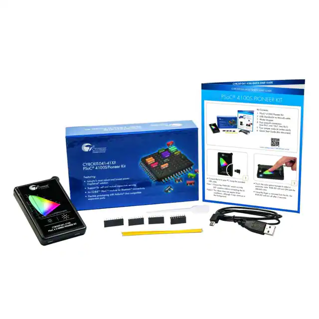
Kit Contents
The CY8CKIT-041-41XX PSoC 4100S Pioneer Kit contains the following, as shown in Figure 1-1.
■
PSoC 4100S Pioneer Kit
■
USB Standard-A to Micro-B cable
■
Water dropper
■
Four press-fit connectors (one 8×2, one 10×1, two 8×1)
■
Four jumper wires
■
Quick Start Guide
PSoC® 4100S Pioneer Kit Guide, Doc. # 002-14067 Rev. *C
5
�Introduction
Figure 1-1. Kit Contents
Inspect the contents of the kit; if you find any part missing, contact your nearest Cypress sales office
for help: www.cypress.com/support.
1.2
Board Details
As shown in Figure 1-2, the PSoC 4100S Pioneer Kit features a CapSense trackpad, two CapSense
buttons, and a proximity sensor loop (not visible on the case) that allows you to evaluate Cypress’s
fourth-generation CapSense technology. The kit has two user buttons, an RGB LED, and a potentiometer that can be used in your applications. It also has a reset button and three status LEDs. The
kit can be powered from three power sources: USB connector, rechargeable battery, or an external
power supply. The kit can operate at 1.9 V, 3.3 V, and 5 V when powered from the USB connector or
external power supply and will operate at 3 V when powered from the battery. The USB connector is
also used for programming and debugging your application on PSoC 4100S.
PSoC® 4100S Pioneer Kit Guide, Doc. # 002-14067 Rev. *C
6
�Introduction
Figure 1-2. PSoC 4100S Pioneer Kit
1
2
3
7
6
5
4
1. KitProg2 Status LEDs
4. Potentiometer
2. Power LED
3. KitProg2 USB Micro-B connector
5. Reset button
6. User button
7. KitProg2 user button
PSoC® 4100S Pioneer Kit Guide, Doc. # 002-14067 Rev. *C
7
�Introduction
Figure 1-3. PSoC 4100S Pioneer Kit without Overlay
1
2
3
1. CapSense trackpad
2. CapSense buttons
3. Proximity sensor loop
Note: The above figure shows the kit without color gamut overlay
PSoC® 4100S Pioneer Kit Guide, Doc. # 002-14067 Rev. *C
8
�Introduction
Figure 1-4. PSoC 4100S Pioneer Board (Top View)
26
10
25 24
10
23
22
1
21
2
20
19
3
18
4
17
16
15
5
6
7
8 9
10
11 12
10 13
14
��� ,JU1SPH��64#�.JDSP�#�DPOOFDUPS� +�
�
14. RGB LED (LED5)
��� ,JU1SPH��TUBUVT�-&%T� -&%�
�-&%��BOE�-&%�
����
�����,JU1SPH��VTFS�CVUUPO�(SW3)
��� &YUFSOBM�QPXFS�TVQQMZ�IFBEFS� +�
���� 3FDIBSHFBCMF�CBUUFSZ� .-�����)4�
�7�
��� ,JU1SPH�� 14P$��-1
�*�0�IFBEFS� +�
17. User Button (SW2)
5.
Power LED (LED4)
18. Reset button (SW1)
6.
System power (VDD) selection switch (SW6)
���� "SEVJOP�*$41�DPNQBUJCMF�IFBEFS� +��
��� ,JU1SPH��DVTUPN�BQQMJDBUJPO�QSPHSBNNJOH�IFBEFS� +��
20. EZ-BLETM PRoCTM Module (CYBLE-022001-00, U3)
��� 7PMUBHF�SFHVMBUPS�DJSDVJU
21. Potentiometer (R2)
��� 14P$�����4����QJO�QSPHSBN�BOE�EFCVH�IFBEFS� +��
22. VDD source selection switch (SW4)
10. ArduinoTM compatible power and I/O headers
�
+�
�+�
�+��BOE�+�
23. Current measurement selection switch (SW7)
11. 32.768 kHz crystal oscillator (Y1)
���� 7PMUBHF�-FWFM�5SBOTMBUPS�GPS�'�3".� 6��
13. Cypress F-RAM 1Mb (FM24V10-G, U11)
24. PSoC 4100S (CY8C4146AZI-S433, U1)
���� 1SPHSBNNJOH�UBSHFU� 14P$�����4�&;�#-&�13P$�.PEVMF
�
selection switch (SW5)
���� ,JU1SPH��QSPHSBNNFS�BOE�EFCVHHFS���14P$��-1�
(CY8C5868LTI-LP039, U15)
PSoC® 4100S Pioneer Kit Guide, Doc. # 002-14067 Rev. *C
9
�PSoC® 4100S Pioneer Kit Guide, Doc. # 002-14067 Rev. *C
P1_6
P4_0
P4_VDD
P0_1
P0_6
P0_7
GND
P3_6
NC
P5LP0_1
P5LP12_0
P5LP3_0
P5LP12_1
P5LP3_5
P5LP12_6
GND
NC
P4_VDD/IOREF
RESET/RESET
V 3.3/3.3 V
V 5.0/5 V
GND/GND
GND/GND
VIN/Vin
P5LP15_4
P5LP1_6
P5LP0_7
P5LP0_3
P5LP0_2
P5LP_VDD
P5LP15_1
P5LP15_2
P5LP15_3
P5LP12_5
P5LP3_4
P5LP12_7
P5LP3_6
P2_0/A0
P2_1/A1
P2_2/A2
P2_3/A3
P2_4/A4
P2_5/A5
P2_6
P3_4
P5LP_SWDIO
P5LP_SWDCLK
P5LP_XRES
GND
P5LP_VBUS
P0_2/D7
P3_7/D6
P3_5/D5
P1_5/D4
P1_3/D3
P1_4/D2
P0_5/D1
P0_4/D0
P3_0/SCL
P3_1/SDA
P1_7/AREF
GND/GND
P1_2/D13
P1_1/D12
P1_0/D11
P0_0/D10
P2_7/D9
P0_3/D8
Introduction
Figure 1-5. PSoC 4100S Pioneer Board (Bottom View)
27
27. FPC connector
Figure 1-6. PSoC 4100S Pioneer Board Pinout
GND
VIN
1
Arduino Uno R3
PSoC 4100S Pioneer Kit
10
�Introduction
Table 1-1. Switches Default Position
Switch
Purpose
SW4 (PWR SEL) VDD Source Selection
1.3
Default Position
EXT (VREG/VBUS)
SW5
Programming Target Selection
PSoC 4100S
SW6
System Power (VDD) Selection
5V
SW7
Current Measurement Selection
Switches P1, P2, P3, and P4 – OFF; Switch P5 – ON
PSoC Creator
PSoC Creator is a state-of-the-art, easy-to-use IDE. It introduces revolutionary hardware and software co-design, powered by a library of fully-verified and characterized PSoC Components™, as
shown in Figure 1-7. With PSoC Creator, you can:
1. Drag and drop Components to build your hardware system design in the main design workspace
2. Co-design your application firmware with the PSoC hardware
3. Configure Components using configuration tools
4. Explore the library of 100+ Components
5. Access Component datasheets
Figure 1-7. PSoC Creator Features
PSoC Creator also enables you to tap into an entire tool ecosystem with integrated compiler chains
and production programmers for PSoC devices.
For more information, visit www.cypress.com/psoccreator.
PSoC® 4100S Pioneer Kit Guide, Doc. # 002-14067 Rev. *C
11
�Introduction
1.3.1
PSoC Creator Code Examples
PSoC Creator includes a large number of code examples. These examples are accessible from the
PSoC Creator Start Page, as shown in Figure 1-8.
Code examples can speed up your design process by starting you off with a complete design. The
code examples also show how to use PSoC Creator Components for various applications. Code
examples and documentation are included, as shown in Figure 1-9.
In the Find Code Example dialog shown in Figure 1-9, you have several options:
■
Filter for examples based on device family or keyword.
■
Select from the list of examples offered based on the Filter Options.
■
View the project documentation for the selection (on the Documentation tab).
■
View the code for the selection on the Sample Code tab. You can also copy and paste code from
this window to your project, which can help speed up code development.
■
Create a new workspace for the code example or add to your existing workspace. This can speed
up your design process by starting you off with a complete, basic design. You can then adapt that
design to your application.
Figure 1-8. Code Examples in PSoC Creator
PSoC® 4100S Pioneer Kit Guide, Doc. # 002-14067 Rev. *C
12
�Introduction
Figure 1-9. Code Example with Sample Code
1.3.2
Kit Code Examples
You can access the installed kit code examples from the PSoC Creator Start Page. To access these
examples, expand the Kits under the section Examples and Kits; then, expand the specific kit to see
the code examples. Refer to the Code Examples chapter on page 32 for a list of code examples that
you can use on this kit.
1.3.3
PSoC Creator Help
Launch PSoC Creator and navigate to the following items:
■
Quick Start Guide: Choose Help > Documentation > Quick Start Guide. This guide gives you
the basics for developing PSoC Creator projects.
■
Simple Component Code Examples: Choose File > Code Example. These examples demonstrate how to configure and use PSoC Creator Components. To access examples related to a
specific Component, right-click on the Component in the schematic or in the Component Catalog.
Select the Find Code Example option in the context menu that appears.
■
System Reference Guide: Choose Help > System Reference > System Reference Guide.
This guide lists and describes the system functions provided by PSoC Creator.
■
Component Datasheets: Right-click a Component and select Open Datasheet. Visit the
PSoC 4 Component Datasheets page for a list of all PSoC 4 Component datasheets.
■
Document Manager: PSoC Creator provides a document manager to help you easily find and
access the document resources. To open the document manager, choose the menu item Help >
Document Manager.
PSoC® 4100S Pioneer Kit Guide, Doc. # 002-14067 Rev. *C
13
�Introduction
1.4
Getting Started
This guide will help you be acquainted with the PSoC 4100S Pioneer Kit:
1.5
■
The Software Installation chapter on page 17 describes the installation of the kit software. This
includes the PSoC Creator IDE to develop and debug the applications, and PSoC Programmer to
program the .hex files on to the device.
■
The Kit Operation chapter on page 20 describes the major features of the PSoC 4100S Pioneer
Kit and functionalities such as programming, debugging, and the USB-UART and USB-I2C
bridges.
■
The Code Examples chapter on page 32 describes multiple PSoC 4100S code examples that will
help you understand how to create your own PSoC 4 projects.
■
The Appendix on page 36 provides the detailed hardware description, method to use the onboard
F-RAM, method to use the on board EZ-BLE PRoC Module, kit schematics, and the bill of materials (BOM).
Additional Learning Resources
Cypress provides a wealth of data at www.cypress.com to help you to select the right PSoC device
for your design, and to help you to quickly and effectively integrate the device into your design. For a
comprehensive list of resources, see KBA86521, How to Design with PSoC 3, PSoC 4, and
PSoC 5LP. The following is an abbreviated list for PSoC 4:
■
Overview: PSoC Portfolio and PSoC Roadmap.
■
Product Selectors: PSoC 4 Product Selector. In addition, PSoC Creator includes a device selection tool.
■
Datasheets: Describe and provide electrical specifications for the PSoC 4000, PSoC 4100,
PSoC 4200, PSoC 4100M, PSoC 4200M, PSoC 4200L, PSoC 4000S and PSoC 4100S device
families.
■
CapSense Design Guide: Learn how to design capacitive touch-sensing applications with the
PSoC 4 family of devices.
■
Application Notes and Code Examples: Cover a broad range of topics, from basic to advanced.
Many of the application notes include code examples. Visit the PSoC 3/4/5 Code Examples web
page for a list of all available PSoC Creator code examples. To access code examples from
within PSoC Creator – see PSoC Creator Code Examples on page 12.
■
Technical Reference Manuals (TRM): Provide detailed descriptions of the architecture and registers in each PSoC 4 device family.
■
Development Kits:
❐
CY8CKIT-041-40XX, CY8CKIT-041-41XX, CY8CKIT-046, CY8CKIT-044, CY8CKIT-042 and
CY8CKIT-040 are easy-to-use and inexpensive development platforms. These kits include
connectors for Arduino-compatible shields. Additionally, CY8CKIT-046, CY8CKIT-044, and
CY8CKIT-042 include connectors for Digilent Pmod Peripheral Modules.
❐
CY8CKIT-049, CY8CKIT-043 and CY8CKIT-145-40XX are very low-cost prototyping platform
for sampling PSoC 4 devices.
❐
CY8CKIT-001 is a common development platform for all PSoC family devices.
❐
■
■
MiniProg3 device provides an interface for flash programming and debug.
Knowledge Base Articles (KBA): Provide design and application tips from experts on using the
device.
Visit www.cypress.com/training for a set of tutorials, including PSoC Creator training. Each tutorial is a series of videos that provide practical examples on various topics starting with basic concepts and moving on to more advanced features.
PSoC® 4100S Pioneer Kit Guide, Doc. # 002-14067 Rev. *C
14
�Introduction
1.6
Technical Support
For assistance, visit Cypress Support or contact customer support at +1(800) 541-4736 Ext. 2 (in the
USA) or +1 (408) 943-2600 Ext. 2 (International).
You can also use the following support resources if you need quick assistance:
1.7
■
Self-help (Technical Documents)
■
Local Sales Office Locations
Documentation Conventions
Table 1-2. Document Conventions for Guides
Convention
1.8
Usage
Courier New
Displays file locations, user entered text, and source code:
C:\...cd\icc\
Italics
Displays file names and reference documentation:
Read about the sourcefile.hex file in the PSoC Creator User Guide.
[Bracketed, Bold]
Displays keyboard commands in procedures:
[Enter] or [Ctrl] [C]
File > Open
Represents menu paths:
File > Open > New Project
Bold
Displays commands, menu paths, and icon names in procedures:
Click the File icon and then click Open.
Times New Roman
Displays an equation:
2+2=4
Text in gray boxes
Describes cautions or unique functionality of the product.
Acronyms
Table 1-3. Acronyms Used in this Document
Acronym
Definition
ADC
analog-to-digital converter
BLE
Bluetooth Low Energy
BOM
bill of materials
CINT
integration capacitor
CMOD
modulator capacitor
CPU
central processing unit
CSD
CapSense Sigma Delta
CTANK
shield tank capacitor
DC
direct current
Del-Sig
Delta-Sigma
ESD
electrostatic discharge
F-RAM
Ferroelectric Random Access Memory
FPC
flexible printed circuit
GPIO
general-purpose input/output
PSoC® 4100S Pioneer Kit Guide, Doc. # 002-14067 Rev. *C
15
�Introduction
Table 1-3. Acronyms Used in this Document (continued)
Acronym
HID
2
Definition
human interface device
I C
inter-integrated circuit
IC
integrated circuit
ICSP
in-circuit serial programming
IDAC
current output digital-to-analog converter
IDE
integrated design environment
LED
light-emitting diode
PC
personal computer
PGA
programmable gain amplifier
PTC
positive temperature coefficient
PRoC
Programmable Radio-on-Chip
PSoC
Programmable System-on-Chip
PWM
pulse-width modulator
RGB
red green blue
SAR
successive approximation register
SPI
serial peripheral interface
SRAM
static random access memory
SWD
serial wire debug
UART
universal asynchronous receiver transmitter
USB
Universal Serial Bus
WCO
watch crystal oscillator
PSoC® 4100S Pioneer Kit Guide, Doc. # 002-14067 Rev. *C
16
�2.
Software Installation
This chapter describes the steps to install the software tools and packages on a PC to use the PSoC
4100S Pioneer Kit. This includes the IDE on which the projects are built and programmed.
2.1
Before You Begin
To install Cypress software, you will require administrator privileges. However, they are not required
to run software that is already installed. Before you install the kit software, close any other Cypress
software that is currently running.
2.2
Install Software
Follow these steps to install the PSoC 4100S Pioneer Kit software:
1. Download the CY8CKIT-041-41XX PSoC 4100S Pioneer Kit software from www.cypress.com/
CY8CKIT-041-41XX. The kit software is available in three different formats for download.
a. CY8CKIT-041-41XX Kit Complete Setup: This installation package contains the files related
to the kit including PSoC Creator and PSoC Programmer. However, it does not include the
Windows Installer or Microsoft .NET framework packages. If these packages are not on your
computer, the installer directs you to download and install them from the Internet.
b. CY8CKIT-041-41XX Kit Only: This executable file installs only the kit contents, which include
kit code examples, hardware files, and user documents. This package can be used if all the
software prerequisites (listed in step 5) are installed on your PC.
c. CY8CKIT-041-41XX DVD ISO: This file is a complete package, stored in a DVD-ROM image
format, which you can use to create a DVD or extract using an ISO extraction program such
as WinZip® or WinRAR. The file can also be mounted similar to a virtual CD/DVD using virtual
drive programs such as Virtual CloneDrive and MagicISO. This file includes all the required
software, utilities, drivers, hardware files, and user documents.
2. If you have downloaded the ISO file, mount it on a virtual drive. Extract the ISO contents if you do
not have a virtual drive to mount. Double-click cyautorun.exe in the root directory of the extracted
content or the mounted ISO if “Autorun from CD/DVD” is not enabled on the computer. The installation window will appear automatically.
Note: If you are using the “Kit Complete Setup” or “Kit Only” file, then go to step 4 for installation.
PSoC® 4100S Pioneer Kit Guide, Doc. # 002-14067 Rev. *C
17
�Software Installation
3. Click Install CY8CKIT-041-41XX to start the PSoC 4100S Pioneer Kit installation, as shown in
Figure 2-1.
Figure 2-1. Kit Installer Screen
4. Select the folder in which you want to install the PSoC 4100S Pioneer Kit-related files. Choose
the directory and click Next.
5. When you click Next, the installer automatically installs the required software, if it is not present
on your computer. Following are the required software:
a. PSoC Creator 4.0 or later: This software is available for download separately at
www.cypress.com/psoccreator.
b. PSoC Programmer 3.25 or later: This is installed as part of the PSoC Creator installation or is
available separately at www.cypress.com/programmer.
6. Choose the Typical, Custom, or Complete installation type (select Typical if you do not know
which one to select) in the Product Installation Overview window, as shown in Figure 2-2. Click
Next after you select the installation type.
PSoC® 4100S Pioneer Kit Guide, Doc. # 002-14067 Rev. *C
18
�Software Installation
Figure 2-2. Product Installation Overview
7. Read the license agreement and select I accept the terms in the license agreement to continue with the installation. Click Next.
8. When the installation begins, a list of packages appears on the installation page. A green check
mark appears next to each package after successful installation.
9. Enter your contact information or select the Continue Without Contact Information check box.
Click Finish to complete the CY8CKIT-041-41XX PSoC 4100S Pioneer Kit software installation.
10.After the installation is complete, the kit contents are available at the following location:
\CY8CKIT-041-41XX PSoC 4100S Pioneer Kit
Default location:
Windows 7 (64-bit): C:\Program Files (x86)\Cypress\CY8CKIT-041-41XX PSoC 4100S
Pioneer Kit
Windows 7 (32-bit): C:\Program Files\Cypress\CY8CKIT-041-41XX PSoC 4100S Pioneer Kit
Note: For Windows 7/8/8.1/10 users, the installed files and the folder are read-only. To use the
installed code examples, follow the steps outlined in the Code Examples chapter on page 32. These
steps will create an editable copy of the example in a path that you choose so the original installed
example is not modified.
2.3
Uninstall Software
The software can be uninstalled using one of the following methods:
■
Go to Start > All Programs > Cypress > Cypress Update Manager and select the Uninstall
button that corresponds to the kit software.
■
Go to Start > Control Panel > Programs and Features for Windows 7 or Add/Remove Programs for Windows XP; choose the product and select the Uninstall/Change button.
PSoC® 4100S Pioneer Kit Guide, Doc. # 002-14067 Rev. *C
19
�3.
Kit Operation
This chapter introduces you to the various features of the PSoC 4100S Pioneer Kit, including the
theory of operation and the onboard programming and debugging functionality, and the KitProg2
USB-UART and USB-I2C bridges.
3.1
Theory of Operation
The PSoC 4100S Pioneer Kit is built around the PSoC 4100S device. Figure 3-1 shows the block
diagram of the PSoC 4100S device.
Figure 3-1. PSoC 4100S Block Diagram
PSoC® 4 One-Chip Solution
MCU Subsystem
Programmable Analog
Blocks
Opamp
x2
I/O Subsystem
GPIO x8
Smart
I/O
SAR ADC
Flash
(16KB to 64KB)
SRAM
(4KB to 8KB)
CMP
x2
7-bit IDAC
x2
Single-Slope
ADC
CapSense
Programmable Digital
Blocks
WCO
TCPWM x5
Serial Wire Debug
SCB x3
Programmable Interconnect and Routing
48 MHz
Advanced High-Performance Bus (AHB)
Cortex®-M0+
GPIO x8
Smart
I/O
GPIOx8
GPIO x8
GPIO x4
Given below is a list of major features of PSoC 4100S device.
■
32-Bit MCU Subsystem
PSoC® 4100S Pioneer Kit Guide, Doc. # 002-14067 Rev. *C
20
�Kit Operation
■
❐
48-MHz ARM® Cortex®-M0+ CPU
❐
Up to 64KB flash, 8KB SRAM
❐
Real-time clock capability with a WCO
Programmable Analog Blocks
❐
One 12-bit, 1-Msps SAR ADC
❐
One 10-bit, 46.8-Ksps Single-Slope ADC
❐
Two opamps configurable as PGAs, comparators, etc.
❐
Two low-power comparators (CMP)
❐
❐
■
■
One CapSense® block that supports low-power operation with self- and mutual-capacitance
sensing
Two 7-bit IDACs configurable as a single 8-bit IDAC
Programmable Digital Blocks
❐
Five 16-bit Timer, Counter, PWM (TCPWM) blocks
❐
Three serial communication blocks (SCBs) that are configurable as I2C, SPI or UART
Packages
❐
35-ball WLCSP, 32-pin QFN, 40-pin QFN, 48-pin TQFPUp to 36 GPIOs, including
16 Smart I/Os
Refer to the PSoC 4100S datasheet for more details on the device features.
Figure 3-2 shows the block diagram for the PSoC 4100S Pioneer Kit.
Figure 3-2. Block Diagram of PSoC 4100S Pioneer Kit
���
��+
�����
��� �
���
%�2�
��
����
�
'�
�7�
�,����
�
���
��
��
�8*�(���
�
�
� ��
�
��+� �,"
(��������
�
�
�
� ��
�
��+� �,"
�
�
�?2'��
�
�
����
����
�����
������� ���
���+
��
��
� ����� ���,�
��"
� �
�
���� �����
����
�%9�%��"
���
���
��������!
"��"##
$�%�!��
��+
�������7�
���)
��+
��)�
� ��
��$���+� �,"
(�� ��
�)�
� ���
�('&��(*��#"
��������!
"��"##
$�%�!��
�
�
���
��
���
�?2'��
�����
�
(�� ��
�
�
���� ���
��7��
����)$�"
�
�
���
��
���
����
����
/�
�
�
J&��!�� �
����
Q�UU�
�#'����
!�%�
�?<
$-���������
.���)%���*�
���
�*&�$@
�0-:;"
&�
��
'� �
�
.
�
*��
��� ��
� �
��
��
�
�
���
� �
����
&�'�
�)����2 '"
1� ����-�
���������"
����
�
���
/�
*���6�����
��
'� �
�
� �
�
����
�
���
�!��
�+� �,
���
�
�����
�����3455�
����
���
� ��
�
� � �������
&�
��'� �
1� ����-
���������#�$%�
�
��
�
������������ ���
������� ��
��
��
�
���������
������
������!�"
�
�
�
'� �
�/
�
���
������
���
��$��
��
��
�0/-"
�?<
#
����������
�
$�%���
� ���
�����
������� ���
�$�%�
��
� ����� ���,�
��"
�����3455�
�&�%��
'��
��*�!
�&�%��
PSoC® 4100S Pioneer Kit Guide, Doc. # 002-14067 Rev. *C
21
�Kit Operation
The PSoC 4100S Pioneer Kit comes with a case that has the PSoC 4100S Pioneer board (main
board) and a Flex PCB. Refer to How to Open the Kit Case on page 26 for details on opening the
case.
Figure 3-3 shows the markup of the PSoC 4100S Pioneer board and the CapSense Flex PCB.
Figure 3-3. PSoC 4100S Pioneer Board and Flex PCB
Proximity sensor loop
Main board
CapSense trackpad
CapSense buttons
Flex PCB
■
PSoC 4100S Pioneer Board (main board)
The PSoC 4100S Pioneer board contains the PSoC 4100S device, KitProg2 circuit, rechargeable
battery, EZ-BLE PRoC Module, F-RAM, switches, LEDs and a voltage regulator.
■
CapSense Flex PCB
The Flex PCB has CapSense sensors including buttons, trackpad, and proximity. The Flex PCB
has two capacitive sensing buttons, a trackpad with seven row and seven column sensors, and a
proximity sensor loop that is used for CapSense proximity sensing.
PSoC® 4100S Pioneer Kit Guide, Doc. # 002-14067 Rev. *C
22
�Kit Operation
Figure 3-4 and Figure 3-5 shows the markup of the PSoC 4100S Pioneer board.
Figure 3-4. PSoC 4100S Pioneer Board (Top View)
26
10
25 24
10
23
22
1
21
2
20
19
3
18
4
17
16
15
5
6
7
8 9
10
11 12
10 13
14
��� ,JU1SPH��64#�.JDSP�#�DPOOFDUPS� +�
�
14. RGB LED (LED5)
��� ,JU1SPH��TUBUVT�-&%T� -&%�
�-&%��BOE�-&%�
����
�����,JU1SPH��VTFS�CVUUPO�(SW3)
��� &YUFSOBM�QPXFS�TVQQMZ�IFBEFS� +�
���� 3FDIBSHFBCMF�CBUUFSZ� .-�����)4�
�7�
��� ,JU1SPH�� 14P$��-1
�*�0�IFBEFS� +�
17. User Button (SW2)
5.
Power LED (LED4)
18. Reset button (SW1)
6.
System power (VDD) selection switch (SW6)
���� "SEVJOP�*$41�DPNQBUJCMF�IFBEFS� +��
��� ,JU1SPH��DVTUPN�BQQMJDBUJPO�QSPHSBNNJOH�IFBEFS� +��
20. EZ-BLETM PRoCTM Module (CYBLE-022001-00, U3)
��� 7PMUBHF�SFHVMBUPS�DJSDVJU
21. Potentiometer (R2)
��� 14P$�����4����QJO�QSPHSBN�BOE�EFCVH�IFBEFS� +��
22. VDD source selection switch (SW4)
10. ArduinoTM compatible power and I/O headers
�
+�
�+�
�+��BOE�+�
23. Current measurement selection switch (SW7)
11. 32.768 kHz crystal oscillator (Y1)
���� 7PMUBHF�-FWFM�5SBOTMBUPS�GPS�'�3".� 6��
13. Cypress F-RAM 1Mb (FM24V10-G, U11)
24. PSoC 4100S (CY8C4146AZI-S433, U1)
���� 1SPHSBNNJOH�UBSHFU� 14P$�����4�&;�#-&�13P$�.PEVMF
�
selection switch (SW5)
���� ,JU1SPH��QSPHSBNNFS�BOE�EFCVHHFS���14P$��-1�
(CY8C5868LTI-LP039, U15)
PSoC® 4100S Pioneer Kit Guide, Doc. # 002-14067 Rev. *C
23
�Kit Operation
Figure 3-5. PSoC 4100S Pioneer Board (Bottom View)
27
27. FPC connector
The PSoC 4100S Pioneer board has the following peripherals:
1. KitProg2 USB Micro-B connector (J6): The USB cable provided along with the PSoC 4100S
Pioneer Kit connects between this USB connector and the PC.
2. KitProg2 Status LEDs: Red, amber, and green LEDs (LED1, LED2, and LED3) indicate the status of the KitProg2. For details on the KitProg2 status, refer to the KitProg2 User Guide.
3. External power supply (VIN) header (J7): This header connects the external power supply
input to the onboard regulator. The voltage input from the external supply can be between 6 V
and 12 V.
4. KitProg2 I/O header (J8): This header brings out a few GPIOs of the onboard PSoC 5LP. This
includes the USB-I2C bridge and USB-UART bridge lines. The additional PSoC 5LP pins are
direct connections to the internal programmable analog logic of PSoC 5LP. You can also use
these pins for custom applications. For more details on the KitProg2, refer to the KitProg2 User
Guide.
5. Power LED (LED4): The amber power LED turns on when the kit is connected to a power
source.
6. System power (VDD) selection switch (SW6): This switch selects the kit operating voltage. It
can select between 1.9 V, 3.3 V, and 5 V.
7. KitProg2 custom application/programming header (J11): This header brings out more GPIOs
of the PSoC 5LP. It also contains a 5-pin SWD programming header for PSoC 5LP.
8. Voltage regulator circuit: The kit can operate at four voltage levels, 1.9 V, 3.3 V, 5 V from USB
or external power supply, and 3 V from the rechargeable battery. The kit has an onboard twochannel regulator from Cypress that provides 3.3 V on one channel and 1.9 V on the other. 3 V is
derived from the onboard battery and 5 V from the USB.
9. PSoC 4100S 10-pin program and debug header (J13): This 10-pin header allows you to program and debug the PSoC 4100S using an external programmer such as MiniProg3. This header
is not populated by default.
PSoC® 4100S Pioneer Kit Guide, Doc. # 002-14067 Rev. *C
24
�Kit Operation
10.Arduino-compatible power and I/O headers: This kit is compatible and operates flawlessly with
third-party Arduino shields. The Arduino-compatible power header (J1) powers Arduino shields.
This header also has the provision to power the kit though the VIN input pin. The Arduino-compatible I/O headers (J1, J2, J3, and J4) bring out the pins from PSoC 4100S to interface with the
Arduino shields.
11. 32.768-kHz crystal oscillator (Y1): This kit has a 32.768-kHz crystal oscillator to provide an
accurate low-frequency clock for the PSoC 4100S.
12.Voltage level translator for F-RAM (U14): The F-RAM operates at 3.3 V, while the PSoC 4100S
can operate at 1.9 V, 3.3 V, 5 V, or 3 V. This bidirectional level translator translates the I2C signals
between the F-RAM and the PSoC 4100S.
13.Cypress F-RAM (U11): This kit features a Cypress F-RAM device (FM24V10-G) of 1 Mb capacity. The F-RAM is connected to the I2C interface of the PSoC 4100S. The F-RAM device can be
used similar to an external EEPROM memory for data logging operations. Refer to Using the
FM24V10 F-RAM on page 44 for details on using the F-RAM.
14.RGB LED (LED5): The onboard RGB LED can be controlled from the PSoC 4100S.
15.KitProg2 user button (SW3): This button is used to switch between the KitPorg2 modes. You
can also use this button to provide input to the PSoC 5LP in custom applications. Note that the
switch connects the PSoC 5LP pin to ground when pressed. Refer to the KitProg2 User Guide for
more details.
16.Rechargeable battery (V2): This kit features an onboard rechargeable battery (ML2430-HS1) to
power the kit at 3 V.
17.User button (SW2): This button can be used to provide input to the PSoC 4100S. Note that the
switch connects the PSoC 4100S pin to ground when pressed; therefore, you need to configure
the PSoC 4100S pin as resistive pull-up to detect switch press.
18.Reset button (SW1): This button is used to reset the PSoC 4100S and EZ-BLE PRoC Module.
19. Arduino ICSP-compatible header (J12): This kit features an Arduino ICSP-compatible header
for SPI interface.
20.EZ-BLE PRoC Module (U3): The kit includes a Cypress EZ-BLE PRoC Module which can be
used for custom applications.
21.Potentiometer (R2): This kit features a potentiometer, which connects to an ADC input pin of the
PSoC 4100S.
22.VDD source selection switch (SW4): This switch selects the power source for the kit between
USB connector/external power supply and battery.
23.Current measurement selection switch (SW7): This switch is used to measure the PSoC
4100S current consumption by turning off all the switches of SW7 and connecting an ammeter
between VDD and P4.VDD test points. Refer to Current Measurement Switch on page 39 for
more details on how to measure the current.
24.PSoC 4100S (U1): This kit is designed to highlight the features of the PSoC 4100S device
(CY8C4146AZI-S433).
25.Programming target selection switch (SW5): This switch selects the SWD lines between
PSoC 4100S or EZ-BLE PRoC Module for programming and debugging.
26.KitProg2 (PSoC 5LP) programmer and debugger (U15): The PSoC 5LP device
(CY8C5868LTI-LP039) serving as KitProg2, is a multi-functional system, which includes a programmer, debugger, USB-I2C bridge, and a USB-UART bridge. Refer to the KitProg2 User Guide
for more details.
27.FPC connector (J10): This connects the Flex PCB to the main board.
See Hardware Functional Description on page 36 for details on various hardware blocks.
PSoC® 4100S Pioneer Kit Guide, Doc. # 002-14067 Rev. *C
25
�Kit Operation
3.1.1
How to Open the Kit Case
The kit comes with a case that houses an FR4 board called the PSoC 4100S Pioneer board (main
board) and a Flex PCB. The following steps show how to open the case.
1. Pull out the bottom case by inserting the finger or a sharp edge object (e.g. a plectrum) in the
notch provided, as shown in Figure 3-6.
Note: Do not use your nails to remove the kit case.
Figure 3-6. Opening the Bottom Case
2. Remove the bottom case by gradually pulling along the edge of bottom case, as shown in
Figure 3-7.
Figure 3-7. Removing the Bottom Case
PSoC® 4100S Pioneer Kit Guide, Doc. # 002-14067 Rev. *C
26
�Kit Operation
3. Hold the kit as shown in Figure 3-8 and pull the bottom side of the casing wall outwards. Hold the
USB connector and lift the board gently.
Figure 3-8. Pull the Main Board from the Case
Note that the main board needs to be removed slowly because it is connected to the Flex PCB. Flex
PCB is permanently attached to the top case. Do not attempt to separate the Flex PCB from the top
case. Instead, disconnect the Flex PCB from the main board by releasing the FPC connector, J10
(see Figure 3-9). The main board can be used for developing your own applications. Arduino shields
can be plugged into the main board using press-fit connectors provided with the kit.
3.1.2
Disconnecting Flex PCB from main board
The FPC connector, J10, is used to connect Flex PCB to the main board. To disconnect the Flex
PCB from the main board, flip up the latches of the FPC connector and pull out the Flex PCB.
Figure 3-9 shows the sequence of steps to be followed.
Figure 3-9. Disconnecting Flex PCB from Main Board
PSoC® 4100S Pioneer Kit Guide, Doc. # 002-14067 Rev. *C
27
�Kit Operation
3.1.3
Reassembling Kit Case
1. Connect the Flex PCB to the main board.
2. Flip the main board and gently push the Flex PCB under the main board.
3. Align the main board switches with respective slots on the top case.
4. Push the main board switches into the slots gently.
5. At the other end of the main board, gently press the board until you hear the click sound.
Note: Make sure the onboard components or switch positions are not changed.
6. Hold the bottom case, align it to the potentiometer and Power Selection switch.
7. Press on all corners to close the bottom case.
3.1.4
Removing the Overlay
The kit case comes with an attached overlay that is imprinted with a CIE 1931 color gamut. This
overlay is intended to be used with the CE214025 Trackpad With Color Gamut code example, which is
pre-programmed into the PSoC 4100S Pioneer Kit. You can remove this if you intend to use the
trackpad without an overlay. Follow these steps to remove the overlay.
1. Hold the kit firmly and pull out the overlay from the corner, as shown in Figure 3-10. Use a sharp
edge object (e.g. a plectrum or a credit card) to pull the overlay from the corner.
Note: Do not use your nails to remove the Overlay.
Figure 3-10. Removing the Overlay
2. Slowly lift the overlay off the case.
After removing the overlay, keep it in a dust-free place for longevity of the micro-suction tape.
PSoC® 4100S Pioneer Kit Guide, Doc. # 002-14067 Rev. *C
28
�Kit Operation
3.1.5
Attaching the Overlay
The overlay has micro-suction tape on the bottom, which allows you to attach the overlay to the kit,
when required. Follow these steps to attach the overlay:
1. Keep the kit on a flat surface. Align the top-left corner of the overlay to the corner edge of the top
case, as shown in Figure 3-11.
Figure 3-11. Attaching the Overlay
2. Place the top edge of the overlay first; then, slide your finger along the overlay surface.
3.2
KitProg2
The PSoC 4100S Pioneer Kit can be programmed and debugged using the onboard KitProg2. The
KitProg2 is a multi-functional system, which includes a programmer, debugger, USB-I2C bridge, and
USB-UART bridge. The PSoC 4100S Pioneer Kit also supports mass storage programming using
KitProg2. A Cypress PSoC 5LP device is used to implement the KitProg2 functionality. The KitProg2
is integrated in most PSoC development kits. For more details on the KitProg2 functionality, refer to
the KitProg2 User Guide available in the following path in the kit installation directory:
\CY8CKIT-041-41XX PSoC 4100S Pioneer Kit\\
Documentation\KitProg2_User_Guide.pdf
Before programming the device, ensure that PSoC Creator and PSoC Programmer are installed on
the computer. See Install Software on page 17 for more information.
3.2.1
Programming and Debugging using PSoC Creator
Ensure switch SW5 is in the “PSoC 4100S” position to select the PSoC 4100S as the target device
for programming. In the other position, the EZ-BLE PRoC Module on the kit can be programmed
(see Programming the EZ-BLE PRoC Module on page 30).
1. Connect the PSoC 4100S Pioneer Kit to the PC using the USB cable, as shown in Figure 3-12.
The kit enumerates as a composite device if you are connecting it to your PC for the first time.
The successful enumeration is indicated by the following status LEDs: amber LED On, green
LED Off and red LED Off. If you do not see the desired LED status, refer to the KitProg2 User
Guide for details on the KitProg2 status and troubleshooting instructions.
PSoC® 4100S Pioneer Kit Guide, Doc. # 002-14067 Rev. *C
29
�Kit Operation
Figure 3-12. Connect USB Cable to USB Connector on the Kit
2. Open the desired project in PSoC Creator by selecting File > Open > Project/Workspace. This
provides the option to browse and open your saved project.
3. Select Build > Build Project or press [Shift] [F6] to build the project.
4. If there are no errors during build, select Debug > Program or press [Ctrl] [F5]. This programs
the device on the PSoC 4100S Pioneer Kit.
The PSoC Creator has an integrated debugger. You can start the debugger by selecting Debug >
Debug or by pressing [F5]. Refer to the Debugging Using PSoC Creator section in the KitProg2
User Guide for a detailed explanation on how to debug using PSoC Creator.
3.2.2
Programming using PSoC Programmer
PSoC Programmer (3.25 or later) can be used to program existing .hex files into the PSoC 4100S
Pioneer Kit. Refer to the Programming Using PSoC Programmer section in the KitProg2 User
Guide for a detailed explanation on how to program using PSoC Programmer.
The KitProg2 firmware normally does not require any update. If necessary, you can use PSoC Programmer to update the KitProg2 firmware. Refer to the Updating the KitProg2 Firmware section in
the KitProg2 User Guide for a detailed explanation on how to update the KitProg2 firmware.
3.2.3
Programming the EZ-BLE PRoC Module
To program the EZ-BLE PRoC Module, follow the instructions provided in Programming and Debugging using PSoC Creator on page 29. The only exception is to set switch SW5 to the “EZ-BLE” position to select the EZ-BLE PRoC Module as the target device for programming.
PSoC® 4100S Pioneer Kit Guide, Doc. # 002-14067 Rev. *C
30
�Kit Operation
3.2.4
Mass Storage Programmer
The KitProg2 in the PSoC 4100S Pioneer Kit supports programming through a USB Mass Storage
interface. This interface allows you to program the PSoC 4100S by copying .hex files into an emulated USB Mass Storage device. For more details on KitProg2 Mass Storage Programmer, refer to
the KitProg2 User Guide.
3.2.5
USB-UART Bridge
The KitProg2 on the PSoC 4100S Pioneer Kit can act as a USB-UART bridge. The UART lines
between the PSoC 4100S and the KitProg2 are hard-wired on the board, with UART_RX assigned to
P0[4] and UART_TX assigned to P0[5] on PSoC 4100S. For more details on the KitProg2 USBUART functionality, refer to the KitProg2 User Guide.
Figure 3-13. UART Connection between KitProg2 and PSoC 4100S
UART
PSoC 4100S
KitProg2
P12[6]
P12[7]
3.2.6
TX
UART TX
RX
RX
UART RX
TX
P0[4]
P0[5]
USB-I2C Bridge
The KitProg2 can function as a USB-I2C bridge and communicate with the Bridge Control Panel
(BCP) software. The I2C lines on the PSoC 4100S device are P3[1] (SDA) and P3[0] (SCL), which
are hard-wired on the board to the I2C lines of the KitProg2. The USB-I2C supports I2C speeds of
50 kHz, 100 kHz, 400 kHz, and 1 MHz. For more details on the KitProg2 USB-I2C functionality, refer
to the KitProg2 User Guide.
Figure 3-14. I2C Connection between KitProg2 and PSoC 4100S
KitProg2
P12[0]
P12[1]
I2C
SCL
SDA
PSoC® 4100S Pioneer Kit Guide, Doc. # 002-14067 Rev. *C
PSoC 4100S
P3[0]
P3[1]
31
�4.
Code Examples
The PSoC 4100S Pioneer Kit includes five code examples. To access the code examples, download
and install the PSoC 4100S Pioneer Kit setup file from www.cypress.com/CY8CKIT-041-41XX. After
installation, the code examples will be available from Examples and Kits > Kits under PSoC Creator Start Page.
For more code examples, visit the PSoC 3, PSoC 4, and PSoC 5 code examples page, which lists all
PSoC Creator code examples available across application notes, kits, and PSoC Creator.
4.1
Using the Kit Code Examples
Follow these steps to open and use the code examples.
1. Launch PSoC Creator from Start > All Programs > Cypress > PSoC Creator >
PSoC Creator .
2. On the Start Page, click CY8CKIT-041-41XX under Examples and Kits > Kits. A list of code
examples appears, as shown in Figure 4-1.
3. Click on the desired code example, select a location to save the project and click OK.
Figure 4-1. Open Code Example from PSoC Creator
4. Build the code example by choosing Build > Build . After the build process is
successful, a .hex file is generated.
PSoC® 4100S Pioneer Kit Guide, Doc. # 002-14067 Rev. *C
32
�Code Examples
5. Connect PSoC 4100S Pioneer Kit to the PC using the USB cable, as shown in Figure 3-12, to
program the kit with the code example.
6. Choose Debug > Program in PSoC Creator.
7. If the device is already acquired, programming will complete automatically – the result will appear
in the PSoC Creator status bar at the bottom left side of the screen. If the device is yet to be
acquired, the Select Debug Target window will appear. Select KitProg2/ and
click the Port Acquire button, as shown in Figure 4-2.
Figure 4-2. Port Acquire
8. After the device is acquired, it is shown in a tree structure below the KitProg2/.
Click Connect and then OK to exit the window and start programming, as shown in Figure 4-3.
Figure 4-3. Connect Device from PSoC Creator and Program
9. After programming is successful, the code example is ready to use.
PSoC® 4100S Pioneer Kit Guide, Doc. # 002-14067 Rev. *C
33
�Code Examples
4.2
Code Examples
Table 4-1 shows a list of code examples that can be used with this kit.
Table 4-1. Code Examples in PSoC Creator
#
Project
Title/Description
1
This code example implements two CapSense buttons using
CY8CKIT-041-41XX. The left button is used to control the onboard
CE214022 LP CapSense RGB LED color, and the right button is used to control the brightness
Buttons
of the RGB LED. Using the low-power modes available in the
PSoC 4100S device, an average current of 5 µA per button is
achieved when the touch is not detected.
2
CE214023 Proximity
Sensing
This code example demonstrates CapSense based proximity
sensing using a PCB trace as a proximity sensor. A proximitysensing distance of 5 cm is achieved using a rectangular loop sensor
with a 9-cm diagonal. Proximity detection is indicated by controlling
the brightness of an LED. The LED has a minimum brightness when
the hand is at a distance of 5 cm; it gradually increases as the hand
approaches the sensor. Using the low-power modes available in the
PSoC 4100S device, an average current of 25 µA is achieved while
detecting the proximity of a hand at 5 cm.
3
This code example implements a CapSense based trackpad as a
user interface. The trackpad has the CIE 1931 color gamut
imprinted; user inputs (touch coordinates) are converted to the
CE214025 Trackpad With
corresponding color coordinates. The RGB LED on the board is
Color Gamut
used to illustrate the chosen color by modulating the associated
signal densities. The brightness of the RGB LED is controlled by
using the two CapSense buttons.
4
CE216873 ADC with
Breathing LED
This code example demonstrates the use of the Sequencing SAR
ADC Component to measure an input voltage on any I/O pin. The
example also shows how to implement a breathing LED using the
Smart IO Component. The breathing LED effect is implemented by
XORing two pulse-width modulation (PWM) signals which have
slightly different frequencies. There are four levels of breathing rates
and three different color LEDs. Depending on the ADC result, a
specific LED and breathing rate is chosen. The ADC result is sent
over I2C to a host PC running Cypress's Bridge Control Panel (BCP)
program.
CE216892 USB-HID
Trackpad
This code example implements a CapSense trackpad and two
button sensors using a PSoC 4100S device. The PSoC device is
interfaced to a Windows PC as a mouse using the USB HID
protocol. The trackpad controls the cursor on the PC and the two
button sensors act as right-click and left-click buttons. To optimize
device power consumption and provide optimum touch response,
this code example implements two power modes: Fast Scan Mode
and Slow Scan Mode.
5
PSoC® 4100S Pioneer Kit Guide, Doc. # 002-14067 Rev. *C
34
�Code Examples
All code examples have an associated PDF document containing the project details, which can be
accessed from the PSoC Creator as shown in the Figure 4-4. Please refer to the respective code
example document for more details on the functionality and implementation.
Figure 4-4. Code Example Document in PSoC Creator
PSoC® 4100S Pioneer Kit Guide, Doc. # 002-14067 Rev. *C
35
�A.
A.1
Appendix
Schematics
Refer to the schematics files available in the kit installation directory under following paths:
A.2
■
\CY8CKIT-041-41XX PSoC 4100S Pioneer Kit\\
Hardware\CY8CKIT-041-41XX Schematic.pdf
■
\CY8CKIT-041-41XX PSoC 4100S Pioneer Kit\\
Hardware\CY8CKIT-041-41XX Flex Schematic.pdf
Hardware Functional Description
This section provides details on the individual hardware blocks of the PSoC 4100S Pioneer Kit.
A.2.1
PSoC 4100S (U1)
This kit features a PSoC 4100S (CY8C4146AZI-S433) family device. PSoC 4100S is a scalable and
reconfigurable platform architecture for a family of programmable embedded system controllers with
an ARM Cortex-M0+ CPU. The PSoC 4100S device family, based on this platform architecture, is a
combination of a microcontroller with programmable analog blocks, programmable digital blocks,
programmable interconnect and routing, CapSense, and standard communication and timing peripherals.
For more information, refer to the PSoC 4100S webpage and the PSoC 4100S family datasheet.
A.2.2
PSoC 5LP (U15)
An onboard PSoC 5LP (CY8C5868LTI-LP039) is used as KitProg2 to program and debug PSoC
4100S. The PSoC 5LP connects to the USB port of a PC through a USB connector and to the SWD
and other communication interfaces of the PSoC 4100S device. The PSoC 5LP is a true systemlevel solution providing MCU, memory, analog, and digital peripheral functions in a single chip. The
CY8C58LPxx family offers a modern method of signal acquisition, signal processing, and control
with high accuracy, high bandwidth, and high flexibility. Analog capability spans the range from thermocouples (near DC voltages) to ultrasonic signals.
For more information, visit the PSoC 5LP webpage. Also, refer to the CY8C58LPxx family datasheet.
A.2.3
Serial Interconnection between PSoC 5LP and PSoC 4100S
In addition to use as an onboard programmer, the PSoC 5LP is used as a USB-Serial interface for
the USB-UART bridge and USB-I2C bridge, as shown in Figure A-1 on page 37. The I2C bus contains firmware-controlled resistive pull-ups using FETs, which can be enabled or disabled using the
PSoC 5LP pins. The USB-Serial pins of the PSoC 5LP are also connected to the I2C/UART pins of
the PSoC 4100S that are available on the Arduino-compatible I/O headers; therefore, the PSoC 5LP
can be used to control Arduino shields with an SPI/I2C/UART interface.
PSoC® 4100S Pioneer Kit Guide, Doc. # 002-14067 Rev. *C
36
�Note: The KitProg2 does not support USB-SPI bridge functionality. The SPI pins of the PSoC 4100S
are connected to the PSoC 5LP for enabling SPI communication between PSoC 5LP and PSoC
4100S for custom PSoC 5LP applications.
Figure A-1. Schematics of Serial Interface Connections and I2C Pull-Up via FETs
VDD
P5LP15_0
4
R113
2.2K
5
1
2
R112
2.2K
3
6
U16
NTZD3152P
R114
P5LP12_1
I2C_SDA
ZERO
R116
P5LP12_0
I2C_SCL
ZERO
I2C Interface
UART TX
UART RX
R52
R47
ZERO
ZERO
J4_P0_4
SPI_MOSI
R40
ZERO
P1_0
NO LOAD
J4_P0_5
UART Interface
SPI_MISO
R42
ZERO
P1_1
NO LOAD
SPI_SCLK
R45
ZERO
P1_2
NO LOAD
I2C_SCL
I2C_SDA
R36
ZERO
R34
ZERO
P3_0
P3_1
I2C Interface
A.2.4
SPI_SSEL
R48
ZERO
P0_0
NO LOAD
SPI Interface
Power Supply System
The power supply system on this board is versatile, allowing the input supply to come from the following sources:
■
5-V power from onboard USB connector
■
6-V to 12-V power from Arduino shield or from external power supply through VIN header (J7)
■
3-V from battery
The PSoC 4100S Pioneer Kit is designed to support 1.9 V, 3.3 V, or 5 V operation for PSoC 4100S
and EZ-BLE PRoC Module, when powered from USB port or external power supply. The voltage
selection is made through switch SW6. The voltage regulator (MB39C011A) from Cypress has two
channels and generates a constant 3.3 V on one channel and 1.9 V on the other. The onboard
rechargeable battery provides 3 V to the kit. The selection between battery and USB is made
through the VDD source selection switch, SW4. When the kit is powered from the USB connector, it
provides 3.3 V and 5 V to the Arduino-compatible power header. Figure A-2 shows the schematics of
the voltage regulator and power selection circuit.
PSoC® 4100S Pioneer Kit Guide, Doc. # 002-14067 Rev. *C
37
�VO_V3.3
LED4
R3
Input Voltage Range 6-12V
CTL
Figure A-2. Schematics of Voltage Regulator Circuit and Power Selection Switch
VCC
1
2
R121
R124
0805
560 ohm
R58
C43
1 nF
30K
AMBER LED
R122
Power LED
P5LP2_7
820 ohm 5%
R55
18K 1%
CTL
13
7
C37
R50
R59
9.1K 1%
6
2.2 nF
10
C36
1.5 nF
6.8K 5%
11
8
9
C39
C40
6.8 nF
6.8 nF
5
REGULATOR
CTL
VCC
-INE1
VH
FB1
VB
-INE2
OUT1-1
FB2
OUT1-2
CSCP1
OUT2-1
CSCP2
OUT2-2
RT
GND
VCC
1
16
C31
1.0 uF
2
OUT1_1
3
OUT1_2
15
OUT2_1
14
OUT2_2
C35
1.0 uF
U8
OUT1_2
L5
1
2
6.8uH
C32
0.1 uF
4
3
OUT2_2
C46
22 uF
4
N1G
P1G
N1D/P1D P1S/P2S
N1S/N2S N2D/P2D
N2G
P2G
8 OUT1_1
C45
C81
10 uF
0.1 uF
7
L6
6
6.8uH
5 OUT2_1
VO_V3.3
12
NO LOAD
TP22
BLACK
NO LOAD
C82
0.1 uF
C42
VCC
DMHC3025LSD
TP11
BLACK
MB39C011A
R44
7.5K 5%
VO_V1.9
U5
Zener 3.3V
C80
R49
5.1K 5%
C88
0.1 uF
0.1 uF
R46
18K 1%
6.8K
R54
910 ohm 1%
15.6K
D8
C47
22 uF
R61
1 nF
R56
820 ohm 5%
R60
20K 1%
2.32K 1%
VBUS
D1
VCC
F2
1
MBR0520L
VIN
2
VO_V3.3
R63
ZERO
D5
PTC Resettable Fuse
V3.3
Voltage Regulator
MBR0520L
VAR_VDD
SW 6
VDD
VO_V1.9 1
VO_V3.3 2
VAR_VDD
1
2
POS1
5
POS2
6
SW 4
5 VO_V1.9
1
6 VO_V3.3
VAR_VDD
POS1
2
POS3
V5.0
3
4
3
4
POS2
7
8
7
V5.0
3
VBAT
1
2 D7
PMEG2010AEB,115
3
8
SPDT
DP3T
SWITCH(SW6) SETTINGS
SW6
POSITION
POS1
Voltage
1.9V
POS2
3.3V
POS3
5.0V
SWITCH(SW4) SETTINGS
SW4
Power Supply
POSITION
POS1
POS2
VREG/VBUS
VBAT
Power Supply Selection
Note:
■
PSoC pins should not be connected to overvoltage/reverse voltage more than what is mentioned
in the datasheet.
■
PSoC pins should not be driven with currents more than what is mentioned in the datasheet.
PSoC® 4100S Pioneer Kit Guide, Doc. # 002-14067 Rev. *C
38
�A.2.5
Battery Charging Circuit
The 3.3 V generated by the regulator is also used to charge the battery as shown in Figure A-3.
Note that the battery charging time is not optimal if the battery is discharged below 2.2 V (dead
threshold). Please refer to the battery datasheet for details.
Figure A-3. Battery Charging Circuit
VO_V3.3
VBAT
V1
1
2
V2
CR2032
3
75 ohm
1
2
DB2J31400L
NO LOAD
3
R39
ML2430-HS1
D2
C83
10 uF
3V Coin-cell Battery
Note: Consider the polarity marks provided on the board while re-soldering the battery.
A.2.6
Protection Circuits
The power supply rail has reverse-voltage, overvoltage, short circuit, and excess current protection
features, as shown in Figure A-4. A PTC resettable fuse is connected to protect the computer's USB
port from shorts and over current. ORing diodes prevent damage to components when the board is
powered from different voltage sources at the same time. The ESD protection is provided for the
USB connector.
Figure A-4. Power Supply Block Diagram with Protection Circuits
A.2.7
Current Measurement Switch
To measure the PSoC 4100S power consumption, switch SW7 is populated in series with the power
supply to the PSoC 4100S which can be used to measure current using an ammeter without the
need to remove any components from the board. The KitProg2 on the board is also able to measure
the power consumption of PSoC 4100S using its internal Del-Sig ADC and SAR ADC. For this purpose, either a 0.86- shunt resistor or 9.76- shunt resistor can be selected using switch SW7. Note
that the contact resistance of the switch is 150 m. The effective shunt resistance achieved will be
1.01 and 9.91 respectively.
PSoC® 4100S Pioneer Kit Guide, Doc. # 002-14067 Rev. *C
39
�SW 7
ZERO
1
P4_VDD
2
R16
3
0.86 Ohm
P5LP0_6
R20
P5LP3_7
VTARG
TP2
RED
NO LOAD
P5LP0_5
VDD
P5LP3_1
Figure A-5. Schematics of Current Measurement Switch
R8
4
9.76 Ohm
R4
5
ZERO
1
3�
10
2
3�
9
3
3�
8
4
3�
7
5
3�
6
10
9
8
7
6
P4_VDD
TP1
RED
NO LOAD
5 POLE DIP SW
SWITCH(S7) SETTINGS
Load
Default
(short)
1 ohm
10 ohm
P1 P2
P3 P4
P5
OFF OFF OFF OFF ON
ON ON
ON OFF OFF
Note: To avoid leakage
during battery operation
remove R20
ON ON OFF ON OFF
By default P5 is ON.
To enable PSoC 5LP Power Monitoring, P1 and P2 should be ON,
P5 should be OFF and the corresponding resistor (1 ohm/ 10 ohm)
should be connected (P3/P4).
To enable external power monitoring, Ammeter should be
connected to TP1 and TP2. P1, P2...P5 should be OFF.
Power Monitoring
The following methods are supported to measure current consumption of the PSoC 4100S device.
■
Measurement using ammeter when powered from USB connector or battery
When the board is powered through the USB connector or battery, turn off all the switches of SW7
and connect an ammeter between P4.VDD and VDD test points, as shown in Figure A-6.
Figure A-6. Current Measurement when Powered from USB Connector or Battery
Note: While measuring the current consumption of the PSoC 4100S device, remove R118 from the
board to get accurate current measurement values.
PSoC® 4100S Pioneer Kit Guide, Doc. # 002-14067 Rev. *C
40
�Figure A-7. Potentiometer Schematics
P4_VDD
R118
3 R2
10K 1
R133
2
ZERO
P2_4
R125
C79
1 nF
ZERO
J2_P2_4
ZERO
NO LOAD
Potentiometer
Remove R118, while performing
low power measurement.
Note that there is a current leakage of 80 µA on the VTARG node into the PSoC 5LP when using
battery (VBAT) as the power supply. Remove resistor R20 to avoid leakage and get accurate current
measurement values. You will not be able to program the PSoC 4100S while you have removed the
resistor. After the measurment is done, populate resistor R20 back to enable programming of the
PSoC 4100S.
After measuring the current consumption, move switch P5 of SW7 to ON position for normal operation of the kit. See Figure A-5 on page 40 for other switch combinations of SW7.
■
Measurement using ammeter when powered from an external power supply
When the PSoC 4100S Pioneer Kit is powered from an external power supply, remove the USB
cable from J6. Connect the positive terminal of the external power supply to the positive terminal of
the ammeter and the negative terminal of the ammeter to the P4.VDD test point. Connect the negative terminal of the external power supply to any GND pin on the board. Figure A-8 shows the
required connections.
Figure A-8. Current Measurement when Powered Externally
VOLTAGE SOURCE
-
+
A.2.8
Expansion Connectors
A.2.8.1
Arduino-compatible Headers (J1, J2, J3, J4, and J12)
This kit has five Arduino-compatible headers: J1, J2, J3, J4, and J12. You can develop applications
based on the Arduino shield hardware.
The J1 header contains I/O pins for reset, internal reference voltage (IOREF), and power supply
lines. The J2 header is an analog port that contains I/O pins for the SAR ADC. The J3 header is pri-
PSoC® 4100S Pioneer Kit Guide, Doc. # 002-14067 Rev. *C
41
�marily a digital port that contains I/O pins for PWM, I2C, SPI, and analog reference. The J4 header is
also a digital port that contains I/O pins for UART and PWM. The J12 header is an Arduino ICSPcompatible header for the SPI interface and is not populated. Most of the pins available on J2, J3,
and J4 headers have multiplexed functionalities such as CapSense sensors, user switch, or RGB
LEDs. See Onboard Peripherals on page 51 for details about onboard peripheral connections to the
pins on these headers.
Note: Pin P1[7] has a provision to connect a 1.0 µF capacitor (C87) as a bypass capacitor for PSoC
4100S SAR ADC. A three-pad 0- resistor (R140 and R141) connects pin P1[7] to the bypass
capacitor or to the CapSense sensor. By default the pin P1[7] is connected to CapSense sensor. If
you intend to use SAR ADC, remove resistor R140 and populate resistor R141. Note that removing
R140 will disconnect Trackpad sensor COL0 from PSoC 4100S device.
A.2.8.2
Additional Functionality of Header J2
The J2 is a 8×2 header that supports Arduino shields. On the non-Arduino side of the header (even
pins – 2, 4, 6, and so on), some pins from port 0, port 1, port 3, and port 4 pins of PSoC 4100S are
brought for general-purpose use.
A.2.8.3
Functionality of Unpopulated Header J12
The J12 is a 3×2 header that supports Arduino shields. This header is used on a small subset of
shields and is not populated on the PSoC 4100S Pioneer Kit.
A.2.8.4
PSoC 5LP GPIO Header (J8)
The J8 is a 8×2 header provided on the kit to bring out several pins of the PSoC 5LP to support
advanced features such as a low-speed oscilloscope and a low-speed digital logic analyzer. This
header also contains the USB-UART bridge pins and USB-I2C bridge pins that can be used when
these pins are not accessible on the Arduino headers because a shield is connected. The additional
PSoC 5LP pins are direct connections to the internal programmable analog logic of PSoC 5LP. This
header also has GPIOs for custom application usage.
A.2.8.5
KitProg2 Custom Application Header (J11)
A 5×2 header is provided on the board to bring out more GPIOs of PSoC 5LP for custom applications. This header also brings out the PSoC 5LP programming pins and can be programmed using
MiniProg3 and 5-pin programming connector.
A.2.9
USB Micro-B Connector
The PSoC 5LP connects to the USB port of a PC through a USB Micro-B connector, which can also
be used to power the PSoC 4100S Pioneer Kit. A resettable polyfuse is used to protect the computer's USB port from shorts and overcurrent. If more than 500 mA is drawn from the USB Micro-B
connector, the fuse will automatically break the connection until the short or overload is removed.
A.2.10
CapSense Circuit
The CapSense sensors such as trackpad, buttons, and proximity sensors are on Flex PCB.
CapSense components such as 560-series resistors on sensor lines, CMOD and CTANK capacitors (essential for the CapSense with self-capacitance functionality), and CintA and CintB capacitors
(essential for CapSense with mutual-capacitance functionality) are on the main board. A 2.2-nF
capacitor is present on the CMOD pin, P4[1], for CapSense operation. This kit also supports
CapSense designs that enable waterproofing. On this kit, the hatch (shield pattern) can be connected to the shield pin, P3[5] or to ground by a three-pad 0- resistor (R75 and R76). By default,
PSoC® 4100S Pioneer Kit Guide, Doc. # 002-14067 Rev. *C
42
�R75 is mounted on the kit, which connects the hatch to the shield pin. This is required for liquid tolerance.
For details on using CapSense, design guidelines, and capacitive sensing, refer to AN85951 - PSoC
4 and PSoC Analog Coprocessor CapSense Design Guide.
A.2.10.1
CapSense Trackpad
The Flex PCB has a 14-element capacitive trackpad, which is connected to the PSoC 4100S pins.
This trackpad controls the LED color in CE214025 Trackpad With Color Gamut code example.
A.2.10.2
CapSense Proximity Sensor
The Flex PCB has one proximity sensor loop, which is connected to pin P1[6]. The proximity senor
loop in the PSoC 4100S Pioneer Kit can also be used as a guard sensor to make the sensors tolerant to streams of liquids.
This proximity sensor controls the LED brightness in CE214023 Proximity Sensing code example.
A.2.10.3
CapSense Buttons
The Flex PCB has two buttons, the left button (BTN1) is connected to pin P0[1] and the right button
(BTN2) is connected to pin P0[2]. These buttons control the LED brightness in CE214025 Trackpad
With Color Gamut code example.
A.2.11
LEDs
The PSoC 4100S Pioneer Kit has five LEDs. Three status LEDs (red, amber, and green) indicate the
status of the KitProg2. An amber LED indicates the status of power supplied to the kit. The kit also
has a general-purpose RGB LED connected to PSoC 4100S for user applications.
A.2.12
Push Buttons
The PSoC 4100S Pioneer Kit has a reset button (SW1) and two user buttons. The reset button is
connected to the XRES pin of the PSoC 4100S and EZ-BLE PRoC Module, and is used to reset both
the devices. One user button (SW2) is connected to P0 [7] of the PSoC 4100S device. The other
user push button (SW3) is connected to P1 [2] of the PSoC 5LP. All the buttons connect to ground on
activation (active low).
A.2.13
Cypress Ferroelectric RAM (F-RAM)
The PSoC 4100S Pioneer Kit contains an F-RAM device (FM24V10-G) that can be accessed
through I2C lines P3 [0] and P3 [1] of the PSoC 4100S. The F-RAM has a capacity of 1-Mbit (128
KB) with an I2C speed up to 3.4 MHz. The I2C slave address of the F-RAM device is 7 bits wide, and
the two least significant bits are configurable through physical pins. These pins are hard-wired to 00
on the board. By default, the address of the F-RAM device used on the kit is 0x50. This address can
be modified by changing the R68/R71 (A1) and R67/R70 (A2) resistor pairs. The operating voltage
range of the F-RAM is between 2 V and 3.6 V. To prevent the F-RAM from operating at voltages
greater than 3.6 V, the power supply to the F-RAM is derived from the output of the 3.3-V regulator.
The I2C lines are connected to the 3.3 V side of the onboard level translator to allow the F-RAM to
communicate with the PSoC 4100S operating at 5 V. For more information on using the F-RAM,
refer to Using the FM24V10 F-RAM on page 44.
A.2.14
EZ-BLE PRoC Module
The PSoC 4100S Pioneer Kit includes an EZ-BLE PRoC Module. The EZ-BLE PRoC Module is a
fully integrated, 10×10×1.8 mm, fully certified, programmable module designed for ease-of-use and
PSoC® 4100S Pioneer Kit Guide, Doc. # 002-14067 Rev. *C
43
�reduced time-to-market. It contains Cypress’s PRoC BLE device, two crystals, chip antenna, shield,
and passive components. For more information on using the EZ-BLE PRoC module, see Using EZBLE PRoC Module on page 46.
A.2.15
External Crystals
The PSoC 4100S Pioneer Kit includes a 32.768-kHz (Y1) external crystal for the WCO input. The
WCO is used to provide an accurate low-frequency clock to PSoC 4100S for Deep-Sleep wake up
intervals, and WDT reset intervals.
A.3
Using the FM24V10 F-RAM
The PSoC 4100S Pioneer Kit has an onboard F-RAM chip that can hold up to 1 Mb of data. The chip
provides an I2C communication interface for data access. It is hard-wired to the I2C interface (P3[0]
and P3[1] of the PSoC 4100S); the same lines are routed to the KitProg2 I2C interface. Because the
F-RAM device is an I2C slave, it can be accessed or shared among various I2C masters on the
same lines. For more details on the F-RAM device, refer to the device datasheet.
A.3.1
Address Selection
The slave address of the F-RAM device consists of three parts, as shown in Figure A-9: slave ID,
device select, and page select. Slave ID is an F-RAM family-specific ID provided in the datasheet of
the particular F-RAM device. For the device used on the PSoC 4100S Pioneer Kit (FM24V10-G), the
slave ID is 1010b. Device select bits are set using the two physical pins A2 and A1 in the device. The
setting of these two pins in PSoC 4100S Pioneer Kit is controlled by resistors R68/R71 (A1) and
R67/R70 (A2). Because the memory location in F-RAM is divided into two pages of 64 KB each, the
page select bit is used to refer to one of the two pages in which the read or write operations will take
place.
Note: The 8-pin SOIC footprint provided for the F-RAM FM24V10 on the PSoC 4100S Pioneer Kit is
compatible with all I2C-based F-RAM devices from Cypress (FM24Vxx, FM24CLxx, and CY15BxxxJ
parts). F-RAM devices with more than 64 KB support only four addresses (four devices of the same
type on the same I2C bus); resistors connected to A1 (R68/R71)) and A2 (R67/R70) pins can be
used to select any of the four addresses. F-RAM devices with less than 64 KB and FM24CLxx parts
support eight addresses; resistors connected to A0 (R69/R72), A1 (R68/R71)) and A2 (R67/R70)
pins can be used to select one of the eight addresses.
Figure A-9. F-RAM I2C Address Byte Structure
A.3.2
High-Speed Mode (Hs-mode)
The FM24V10 supports a 3.4 MHz high-speed mode. A master code (00001XXXb) must be issued
to place the device into high-speed mode. Communication between master and slave will then be
enabled for speeds up to 3.4 MHz. A STOP condition will exit Hs-mode. Single-byte and multiplebyte reads and writes are supported.
PSoC® 4100S Pioneer Kit Guide, Doc. # 002-14067 Rev. *C
44
�Figure A-10. F-RAM I2C Data Format for HS Mode
A.3.3
Write/Read Operation
The F-RAM device datasheet includes details on how to perform a write/read operation with the FRAM. Figure A-11 and Figure A-12 provide a snapshot of the write/read packet structure as a quick
reference.
Figure A-11. F-RAM Single-Byte and Multiple-Byte Write Packet Structure
PSoC® 4100S Pioneer Kit Guide, Doc. # 002-14067 Rev. *C
45
�Figure A-12. F-RAM Single-Byte and Multiple-Byte Read Packet Structure
As the figures show, operations start with the slave address followed by the memory address. For
write operations, the bus master sends the slave address and memory address followed by one or
more data bytes. Each byte of data is written to consecutive locations in the memory, and the memory generates an acknowledgement condition.
For ‘Current Address Read’ and ‘Sequential Read’, the bus master sends only the slave address.
The memory address used is the same address that was set by the previous ‘Write’ or ‘Selective
Read’ operation. For ‘Selective Read’ operations, after receiving the complete slave address and
memory address, the memory will begin shifting data from the current address on the next clock
Note: You can communicate with the F-RAM using the Bridge Control Panel (BCP) software similar
to the way you communicate with any other I2C slave device. Refer to the KitProg2 User Guide for
more details on how to use the BCP to communicate with an I2C slave device. Visit the
CY15FRAMKIT-001 Serial F-RAM Development Kit webpage for code examples and the Arduino
library for interfacing I2C F-RAM devices with the PSoC 4 family. Please note that PSoC 4100S Pioneer Kit needs to be power cycled when the F-RAM I2C is stuck. F-RAM I2C will be stuck if the
PSoC 4100S device is reset while it is communicating with the F-RAM.
A.4
Using EZ-BLE PRoC Module
To get started with the EZ-BLE PRoC module, refer to the application note AN96841 - Getting
Started With EZ-BLE PRoC Module. This application note introduces you to Cypress’s EZ-BLE family of Bluetooth Smart modules, helps you explore the EZ-BLE module architecture and development
tools and shows you how to create your first project with the EZ-BLE PRoC Module and PSoC Creator, the development tool used for all EZ-BLE modules. This application note also guides you to
more resources to accelerate in-depth learning about the Cypress EZ-BLE solutions. Visit
www.cypress.com/ez-bleprocmodule/ for additional information on the EZ-BLE PRoC Module.
The EZ-BLE PRoC module includes the following connections to the PSoC 4100S and KitProg2:
PSoC® 4100S Pioneer Kit Guide, Doc. # 002-14067 Rev. *C
46
�■
■
I2C connections to KitProg2 and PSoC 4100S. See Table A-1 for details.
SWD connections to KitProg2 through switch SW5. The SWD connections are shared between
the PSoC 4100S and EZ-BLE PRoC Module.
The connections between EZ-BLE PRoC Module and PSoC 4100S are shown in Figure A-13
Figure A-13. EZ-BLE PRoC Connections
U3
1
2
3
4
5
BLE_SCL
BLE_SDA
BLE_VDDR
P4.0
P3.6
P1.5
P1.4
BLE_XRES
17
16
15
14
BLE_VDD 13
12
11
10
9
8
7
6
P3.7
P3.4
P3.5
XRES
VDD
P1.7
P0.6
GND2
P0.5
P0.4
P0.7
P1.6
21
20
19
18
GND1
P4.1
P5.1
CYBLE-022001-00 P5.0
VDDR
BLE_SCL
R38
BLE_SDA
ZERO
R37
P3_0
P3_1
ZERO
PRoC BLE and PSoC 4100S
Connections
BLE_SWDCLK
BLE_SWDIO
BLE_XRES
R22
ZERO
RESET
BLE Reset
VDD
BLE_VDD
L1
330 OHM @ 100MHz
C3
BLE_VDDR
4.7uF
L2
330 OHM @ 100MHz
EZ-BLE PRoC Module
Table A-1. EZ-BLE PRoC Connections
EZ-BLE PRoC Module Connections
EZ-BLE
BLE_SDA, P5.0
PSoC 4
P3.1
KitProg2
I2C_SDA, P12.1
Description
GPIO/I2C_SDA
BLE_SCL, P5.1
P3.0
I2C_SCL, P12.0
GPIO/I2C_SCL
BLE_SWDIO, P0.6
–
SWDIO, P12.2
SWD I/O
BLE_SWDCLK, P0.7
–
SWDCLK, P12.3
SWD Clock
To program the EZ-BLE PRoC Module using KitProg2, follow the instructions provided in Programming the EZ-BLE PRoC Module on page 30.
PSoC® 4100S Pioneer Kit Guide, Doc. # 002-14067 Rev. *C
47
�A.5
Migrating Projects Across Different Pioneer Series Kits
All Cypress Pioneer series kits are Arduino Uno-compatible and have some common onboard
peripherals such as RGB LED, CapSense, and user switch. However, the pin mapping in each of the
boards is different due to differences in pin functions of the PSoC device used. This section lists the
pin mapping of the Pioneer series kits to allow for easy migration of projects across different kits.
In some cases, the pins available on the Pioneer kit headers are a superset of the standard Arduino
Uno pins. For example, J2 contains only one row of pins on the Arduino Uno pin layout while it contains two rows of pins on many of the Pioneer series kits.
Figure A-14. Pioneer Series Kits Pin Map
10
1
8
1
J3
J4
Pioneer series kits
2
J1
8
Arduino-compatible
power header
Arduino-compatible
I/O headers
12
20
J2
1
1
11
19
CY8 CKIT- 040
6x1 header
CY8 CKIT-042- BLE
6x2 header
CY8CKIT-041-41XX
8x2 header
CY8 CKIT-042 & CY8 CKIT- 044
9x2 header
CY8 CKIT- 048
10x1 header
PSoC® 4100S Pioneer Kit Guide, Doc. # 002-14067 Rev. *C
48
�A.5.1
Arduino Uno Compatible Headers
Table A-2. J1 Arduino Compatible Header Pin Map
Pioneer Series Kits
#
Arduino Pin
CY8CKIT042
CY8CKIT040
CY8CKIT042-BLE
CY8CKIT044
CY8CKIT046
CY8CKIT041-40XX/
CY8CKIT041-41XX
CY8CKIT048
1
VIN
VIN
VIN
VIN
VIN
VIN
VIN
VIN
2
GND
GND
GND
GND
GND
GND
GND
GND
3
GND
GND
GND
GND
GND
GND
GND
GND
4
5V
V5.0
V5.0
V5.0
V5.0
V5.0
V5.0
V5.0
5
3.3V
V3.3
V3.3
V3.3
V3.3
V3.3
V3.3
V3.3
6
RESET
RESET
RESET
RESET
RESET
RESET
RESET
RESET
7
IOREF
P4.VDD
P4.VDD
BLE.VDD
P4.VDD
P4L.VDD
P4.VDD
PAC.VDD
8
NC
NC
NC
NC
NC
NC
NC
NC
Table A-3. J2 Arduino Compatible Header Pin Map
Pioneer Series Kits
#
Arduino Pin
CY8CKIT042
CY8CKIT040
CY8CKIT042-BLE
CY8CKIT044
CY8CKIT046
CY8CKIT041-40XX/
CY8CKIT041-41XX
CY8CKIT048
1
A0
P2[0]
P0[0]
P3[0]
P2[0]
P2[0]
P2[0]1
P3[0]
2
P0[2]1
P2[0]
P2[6]1
P3[6]1
P1[6]1
3
A1
P2[1]
P0[1]
P3[1]
P2[1]
P2[1]
P2[1]1
P3[1]
4
1
P2[1]1
P6[5]1
P3[7]1
P4[0]1
1
5
A2
P0[3]
P2[2]
P0[2]
1
P3[2]
P2[2]
P2[2]
P2[2]
P0[6]1
P3[2]
6
P4.VDD
P2[2]1
P9[0]
P4.VDD
7
A3
P2[3]
P0[4]1
P3[3]
P2[3]
P2[3]
P2[3]1
P3[3]
8
P1[5]1
P2[3]1
P4[4]1
P9[1]
P0[1]1
1
P3[4]1
9
A4
P2[4]
P1[3]
P3[4]
P2[4]
P2[4]
P2[4]
10
P1[4]1
P2[4]1
P4[5]1
P9[2]
P0[6]1
11
A5
P2[5]
P1[2]
P3[5]
P2[5]
P2[5]
P2[5]
P3[7]1
12
P1[3]1
P2[5]1
P4[6]1
P9[3]
P0[7]1
13
P0[0]
P0[0]
14
GND
GND
GND
15
P0[1]
P0[1]
P3[4]1
P2[5]1
16
P1[2]1
P3[4]1
P3[6]1
17
P1[0]
P0[7]1
P2[1]1
18
P1[1]1
P3[5]1
19
P3[5]1
20
P2[6]
1
P2[6]1
Note 1: These pins are also used for onboard peripherals. Refer to the tables in the A.5.2 Onboard Peripherals
section for connection details.
PSoC® 4100S Pioneer Kit Guide, Doc. # 002-14067 Rev. *C
49
�Table A-4. J3 Arduino Compatible Header Pin Map
Pioneer Series Kits
#
Arduino Pin
CY8CKIT042
CY8CKIT040
CY8CKIT042-BLE
CY8CKIT044
CY8CKIT046
CY8CKIT041-40XX/
CY8CKIT041-41XX
CY8CKIT048
1
D8
P2[6]
P1[4]
P0[5]
P0[2]
P0[2]
P0[3]1
P2[4]1
2
D9
P3[6]
P1[5]
P0[4]
P0[3]
P0[3]
P2[7]
P1[7]1
P6[3]
P0[0]1
P0[7]
1
P0[4]
3
D10
P3[4]
P1[6]
1
P0[2]
P2[7]
4
D11
P3[0]
P1[1]
P0[0]
P6[0]
P6[0]
P1[0]
5
D12
P3[1]
P3[1]
P0[1]
P6[1]
P6[1]
P1[1]1
P0[5]
6
D13
P0[6]
P1[7]
P0[3]
P6[2]
P6[2]
P1[2]1
P0[6]
7
GND
GND
GND
GND
GND
GND
GND
GND
8
AREF
P1[7]
NC
VREF
P1[7]
VREF
P1[7]1
P1[3]1
9
SDA
P4[1]
P1[3]
P3[4]
P4[1]
P4[1]
P3[1]
P4[1]
10
SCL
P4[0]
P1[2]
P3[5]
P4[0]
P4[0]
P3[0]
P4[0]
Note 1: These pins are also used for onboard peripherals. Refer to the tables in the A.5.2 Onboard
Peripherals section for connection details.
Table A-5. J4 Arduino Compatible Header Pin Map
Pioneer Series Kits
#
Arduino Pin
CY8CKIT042
CY8CKIT040
CY8CKIT042-BLE
CY8CKIT044
CY8CKIT046
CY8CKIT041-40XX/
CY8CKIT041-41XX
CY8CKIT048
1
D0
P0[4]
P0[5]
P1[4]
P3[0]
P3[0]
P0[4]
P0[4]
2
P8[0]
3
D1
P0[5]
P0[6]
P1[5]
P3[1]
P3[1]
P0[5]
P0[5]
4
P8[1]
P1[5]1
P0[7]
P1[6]
P1[0]
P1[0]
P1[4]1
P8[2]
P1[7]
P1[1]
P1[1]
P1[3]1
P2[3]1
P8[3]
P1[2]1
5
D2
P0[7]
6
1
7
D3
P3[7]
P3[2]1
8
9
D4
P0[0]
P0[3]
P1[3]
P1[2]
P1[2]
P1[5]1
10
P8[4]
P1[1]1
11
D5
P3[5]
P3[0]
P1[2]
P1[3]
P1[3]
P3[5]1
12
P8[5]
P1[0]1
13
D6
P1[0]
P1[0]
P1[1]
P5[3]
P5[6]
P3[7]1
14
P8[6]
15
D7
P2[7]1
P2[0]
P2[7]1
16
1
P1[0]
P5[5]
P5[5]
P0[2]1
P8[7]
Note 1: These pins are also used for onboard peripherals. Refer to the tables in the A.5.2 Onboard
Peripherals section for connection details.
PSoC® 4100S Pioneer Kit Guide, Doc. # 002-14067 Rev. *C
50
�A.5.2
Onboard Peripherals
Table A-6. CapSense Pin Map
Pioneer Series Kits
#
CapSense Pin
CY8CKIT042
CY8CKIT040
CY8CKIT042-BLE
CY8CKIT044
CY8CKIT046
CY8CKIT041-40XX/
CY8CKIT041-41XX
CY8CKIT048
1
CapSense Sensor 1
P1[1]
P2[1]
P4[4]
P0[6]
P1[7]
2
CapSense Sensor 2
P1[2]
P2[2]
P4[5]
P4[5]
P2[0]
3
CapSense Sensor 3
P1[3]
P2[3]
P4[6]
P4[4]
P2[1]
4
CapSense Sensor 4
P1[4]
P2[4]
P3[4]
P4[7]
P2[2]
5
CapSense Sensor 5
P1[5]
P2[5]
P3[5]
P4[6]
P2[3]
6
CapSense Sensor 6
P7[4]
P0[3]
7
CapSense Sensor 7
P7[5]
P0[6]
8
CapSense Sensor 8
P7[6]
P0[0]
9
CapSense Sensor 9
P7[7]
P1[5]
10
CapSense Sensor 10
P0[0]
P1[0]
11
CapSense Sensor 11
P0[1]
P1[1]
12
CapSense Sensor 12
P7[2]
P1[2]
13
CapSense Sensor 13
P7[3]
P1[3]
14
CapSense Sensor 14
P1[4]
15
CapSense Sensor 15
P0[1]
16
CapSense Sensor 16
P0[2]
17
CapSense Sensor 17
P3[7]
18
CMOD0
P4[2]
P0[4]
P4[0]
P4[2]
P4[2]
P4[1]
19
CTANK0
P4[3]
P0[2]
P4[1]
P4[3]
P4[3]
P4[0]
20
CMOD11
P5[0]
21
CTANK11
P5[1]
22
CintA2
P4[2]
23
CintB2
P4[3]
24
CapSense Shield
P0[1]
P1[6]
P0[1]
P0[2]
P3[5]
Note 1: CMOD1, and CTANK1 are available only in the CY8CKIT-046 PSoC 4 L-Series Pioneer Kit.
Note 2: CintA and CintB are available only in the CY8CKIT-041-40XX and CY8CKIT-041-41XX.
Table A-7. Proximity Header Pin Map
Pioneer Series Kits
#
1
2
Proximity Pin
PROXIMITY
CY8CKIT042
CY8CKIT040
CY8CKIT042-BLE
CY8CKIT044
CY8CKIT046
CY8CKIT041-40XX/
CY8CKIT041-41XX
CY8CKIT048
P2[0]
P2[0]
P3[7]
P9[4]
P1[6]
P3[6]
P9[5]
PSoC® 4100S Pioneer Kit Guide, Doc. # 002-14067 Rev. *C
51
�Table A-8. RGB LED Pin Map
Pioneer Series Kits
LED Pin
CY8CKIT042
CY8CKIT040
CY8CKIT042-BLE
CY8CKIT044
CY8CKIT046
CY8CKIT041-40XX/
CY8CKIT041-41XX
CY8CKIT048
1
Red
P1[6]
P3[2]
P2[6]
P0[6]
P5[2]
P3[4]
P1[4]
2
Green
P0[2]
P1[1]
P3[6]
P2[6]
P5[3]
P2[6]
P2[6]
3
Blue
P0[3]
P0[2]
P3[7]
P6[5]
P5[4]
P3[6]
P1[6]
#
Table A-9. User Switch Pin Map
Pioneer Series Kits
A.6
#
Switch Pin
CY8CKIT042
CY8CKIT040
CY8CKIT042-BLE
CY8CKIT044
CY8CKIT046
CY8CKIT041-40XX/
CY8CKIT041-41XX
CY8CKIT048
1
SW2
P0[7]
P2[7]
P0[7]
P0[7]
P0[7]
P0[3]
Bill of Materials
Refer to the BOM files in the following paths in the kit software installed:
■
\CY8CKIT-041-41XX PSoC 4100S Pioneer Kit\\Hardware\CY8CKIT-041-41XX PCBA BOM.xlsx
■
\CY8CKIT-041-41XX PSoC 4100S Pioneer Kit\\Hardware\CY8CKIT-041-41XX Flex PCBA BOM.xlsx
PSoC® 4100S Pioneer Kit Guide, Doc. # 002-14067 Rev. *C
52
�Revision History
CY8CKIT-041-41XX PSoC® 4100S Pioneer Kit Guide Revision History
Document Title: CY8CKIT-041-41XX PSoC® 4100S Pioneer Kit Guide
Document Number: 002-14067
Revision
ECN
Number
Issue Date
Origin of
Change
Description of Change
**
5361817
07/20/2016
SRDS
New kit guide.
*A
5401322
08/12/2016
SRDS
Updated Introduction chapter on page 5:
Updated “Board Details” on page 6:
Updated Table 1-1.
Updated Kit Operation chapter on page 20:
Updated “Theory of Operation” on page 20:
Updated description and updated Figure 3-1.
Updated “How to Open the Kit Case” on page 26:
Updated description.
Updated “Removing the Overlay” on page 28:
Updated description.
Updated “Attaching the Overlay” on page 29:
Updated description.
Updated Code Examples chapter on page 32:
Updated “Code Examples” on page 34:
Updated Table 4-1, updated description and added Figure 4-4.
Updated Appendix chapter on page 36:
Updated “Hardware Functional Description” on page 36:
Updated “Current Measurement Switch” on page 39:
Updated description.
Updated “CapSense Circuit” on page 42:
Updated description.
Updated “Migrating Projects Across Different Pioneer Series Kits” on
page 48:
Updated “Arduino Uno Compatible Headers” on page 49:
Updated Table A-3.
PSoC® 4100S Pioneer Kit Guide, Doc. # 002-14067 Rev. *C
53
�Index
CY8CKIT-041-41XX PSoC® 4100S Pioneer Kit Guide Revision History (continued)
Document Title: CY8CKIT-041-41XX PSoC® 4100S Pioneer Kit Guide
Document Number: 002-14067
Revision
ECN
Number
Issue Date
Origin of
Change
*B
5444290
09/21/2016
SRDS
Description of Change
Updated Introduction chapter on page 5:
Updated “Board Details” on page 6:
Updated Table 1-1.
Updated Appendix chapter on page 36:
Updated “Hardware Functional Description” on page 36:
Updated “Battery Charging Circuit” on page 39:
Updated description.
*C
5497588
10/27/2016
SRDS
Updated Software Installation chapter on page 17:
Updated “Install Software” on page 17:
Updated description.
Updated Kit Operation chapter on page 20:
Updated “KitProg2” on page 29:
Updated “Programming using PSoC Programmer” on page 30:
Updated description.
Updated Code Examples chapter on page 32:
Updated description.
Updated “Using the Kit Code Examples” on page 32:
Updated Figure 4-1.
Updated “Code Examples” on page 34:
Updated Table 4-1.
PSoC® 4100S Pioneer Kit Guide, Doc. # 002-14067 Rev. *C
54
�