CY8CTMG120
TrueTouch™ Multi-Touch Gesture
Touchscreen Controller
Features
■
TrueTouch™ Capacitive Touchscreen Controller
❐ Supports Single-Touch and Multi-Touch Touchscreen Control
❐ Supports up to 44 X/Y Sensor Inputs
❐ Supports Screen Sizes 8.4” and Below
❐ Fast Scan Rates: Typical 0.5 ms per Sensor
❐ High Resolution: Typical 480 x 360 for 3.5” Screen
❐ Available in 56-Pin QFN Package
❐ Seamless Transition up to Higher Function Multi-Touch
All-Point Device
■
Lowest Noise TrueTouch Device
■
Highly Configurable Sensing Circuitry
❐ Allows Maximum Design Flexibility
❐ Allows Trade-Off Between Scan Time and Noise Performance
■
Includes Gesture Detection Library
■
Develop Customized User Defined Gestures
■
Provides Maximum EMI Immunity
❐ Selectable Spread-Spectrum Clock Source
■
Powerful Harvard Architecture Processor
❐ M8C Processor Speeds to 24 MHz
❐ Two 8x8 Multiply, 32-Bit Accumulate
❐ Low Power at High Speed
❐ 3V to 5.25V Operating Voltage
❐ Industrial Temperature Range: –40°C to +85°C
❐ USB Temperature Range: –10°C to +85°C
■
Full-Speed USB (12 Mbps)
❐ Four Uni-Directional Endpoints
❐ One Bi-Directional Control Endpoint
❐ USB 2.0 Compliant
❐ Dedicated 256 Byte Buffer
❐ No External Crystal Required
■
Flexible On-Chip Memory
❐ 16K Flash Program Storage, 50000 Erase/Write Cycles
❐ 1K SRAM Data Storage
❐ In-System Serial Programming (ISSP)
❐ Partial Flash Updates
❐ Flexible Protection Modes
❐ EEPROM Emulation in Flash
■
Precision, Programmable Clocking
❐ Internal ±4% 24 and 48 MHz Oscillator
❐ Internal Oscillator for Watchdog and Sleep
❐ 0.25% Accuracy for USB with no External Components
Cypress Semiconductor Corporation
Document Number: 001-46929 Rev. *B
•
■
Additional System Resources
2
❐ I C™ Slave, Master, and Multi-Master to 400 kHz
❐ Watchdog and Sleep Timers
❐ User-Configurable Low Voltage Detection
❐ Integrated Supervisory Circuit
❐ On-Chip Precision Voltage Reference
■
Complete Development Tools
❐ Free Development Software (PSoC Designer™)
❐ TrueTouch Touchscreen Tuner
❐ Full-Featured, In-Circuit Emulator and Programmer
❐ Full Speed Emulation
❐ Complex Breakpoint Structure
❐ 128K Bytes Trace Memory
■
Programmable Pin Configurations
❐ 25 mA Sink, 10 mA Drive on All GPIO
❐ Pull Up, Pull Down, High Z, Strong, or Open Drain Drive
Modes on All GPIO
❐ Configurable Interrupt on All GPIO
198 Champion Court
Logic Block Diagram
•
San Jose, CA 95134-1709
•
408-943-2600
Revised July 29, 2008
[+] Feedback
�CY8CTMG120
The TrueTouch family provides the fastest and most efficient way
to develop and tune a capacitive touchscreen application. A
TrueTouch device includes the configurable TrueTouch block,
configurable analog and digital logic, programmable interconnect, and an 8-bit CPU to run custom firmware. This architecture enables the user to create flexible, customized touchscreen configurations to match the requirements of each
individual touchscreen application. Various configurations of
Flash program memory, SRAM data memory, and configurable
IO are included in a range of convenient pinouts.
The Digital System
The Digital System is composed of 4 digital PSoC blocks. Each
block is an 8-bit resource that can be used alone or combined
with other blocks to form 8, 16, 24, and 32-bit peripherals, which
are called user module references.
Figure 1. Digital System Block Diagram
Port 7
Port 5
Port 3
Port 4
Port 1
Port 2
To System Bus
Digital Clocks
FromCore
The TrueTouch architecture is comprised of four main areas: the
Core, Digital System, the TrueTouch Analog System, and
System Resources including a full-speed USB port. Configurable
global busing allows all the device resources to be combined into
a complete custom touchscreen system. The CY8CTMG120
device can have up to seven IO ports that connect to the global
digital and analog interconnects, providing access to four digital
blocks and six analog blocks. Implementation of touchscreen
application allows additional digital and analog resources to be
used, depending on the touchscreen design. The CY8CTMG120
is offered in a 56-pin QFN package, with up to 48 general
purpose IO (GPIO), and support of up to 44 X/Y sensors.
Port 0
ToAnalog
System
DIGITAL SYSTEM
Digital PSoC Block Array
8
When designing touchscreen applications, refer to the UM data
sheet for performance requirements to meet and detailed design
process explanation.
Row0
DBB00
DBB01
DCB02
4
DCB03
4
GIE[7:0]
GIO[7:0]
GlobalDigital
Interconnect
8
Row Output
Configuration
8
Row Input
Configuration
TrueTouch Functional Overview
8
GOE[7:0]
GOO[7:0]
The TrueTouch Core
The core includes a CPU, memory, clocks, and configurable
GPIO (General Purpose IO).
Digital peripheral configurations include those listed below.
The M8C CPU core is a powerful processor with speeds up to 24
MHz, providing a four MIPS 8-bit Harvard architecture microprocessor. The CPU uses an interrupt controller with up to 20
vectors, to simplify programming of real time embedded events.
Program execution is timed and protected using the included
Sleep and Watch Dog Timers (WDT).
■
Full-Speed USB (12 Mbps)
■
PWMs (8 to 32 bit)
■
PWMs with dead band (8 to 24 bit)
■
Counters (8 to 32 bit)
Memory encompasses 16K of Flash for program storage, 1K of
SRAM for data storage, and up to 2K of EEPROM emulated
using the Flash. Program Flash uses four protection levels on
blocks of 64 bytes, allowing customized software IP protection.
■
Timers (8 to 32 bit)
■
UART 8 bit with selectable parity
■
SPI master and slave
The TrueTouch device incorporates flexible internal clock generators, including a 24 MHz IMO (internal main oscillator) accurate
to 8% over temperature and voltage. The 24 MHz IMO can also
be doubled to 48 MHz for use by the digital system. A low power
32 kHz ILO (internal low speed oscillator) is provided for the
Sleep timer and WDT. The clocks, together with programmable
clock dividers (as a System Resource), provide the flexibility to
integrate almost any timing requirement into the PSoC device. In
USB systems, the IMO self-tunes to ± 0.25% accuracy for USB
communication.
■
I2C slave and multi-master
■
Pseudo random sequence generators (8 to 32 bit)
The GPIOs provide connection to the CPU, digital and analog
resources of the device. Each pin’s drive mode may be selected
from eight options, allowing great flexibility in external interfacing. Every pin also has the capability to generate a system
interrupt on high level, low level, and change from last read.
Document Number: 001-46929 Rev. *B
The digital blocks are connected to any GPIO through a series
of global buses that can route any signal to any pin. The buses
also allow signal multiplexing and performing logic operations.
This configurability frees your designs from the constraints of a
fixed peripheral controller.
Digital blocks are provided in rows of four, where the number of
blocks varies by TrueTouch device family. This allows optimum
choice of system resources for your application. Family characteristics are shown in Table 1 on page 4.
Page 2 of 33
[+] Feedback
�CY8CTMG120
Figure 2. Analog System Block Diagram
The Analog System is composed of 6 configurable blocks, each
comprised of an opamp circuit allowing the creation of complex
analog signal flows. Analog peripherals are very flexible and can
be customized to support specific application requirements.
Some of the more common PSoC analog functions (most
available as user modules) are listed below.
Analog-to-digital converters (up to 2, with 6- to 14-bit resolution,
selectable as Incremental, Delta Sigma, and SAR)
■
Filters (2 and 4 pole band-pass, low pass, and notch)
■
Amplifiers (up to 2, with selectable gain to 48x)
■
Instrumentation amplifiers (1 with selectable gain to 93x)
■
Comparators (up to 2, with 16 selectable thresholds)
■
DACs (up to 2, with 6- to 9-bit resolution)
■
Multiplying DACs (up to 2, with 6- to 9-bit resolution)
■
High current output drivers (two with 30 mA drive as a PSoC
Core Resource)
■
1.3V reference (as a System Resource)
■
Modulators
■
Correlators
■
■
P0[7]
P0[6]
P0[5]
P0[4]
P0[3]
P0[2]
P0[1]
P0[0]
AGNDIn RefIn
■
All IO
(Exce p t Port 7)
Analog
Mux Bus
The Analog System
P2[3]
P2[1]
P2[6]
P2[4]
P2[2]
P2[0]
AC I0[1:0]
AC I1[1:0]
Array Inp u t
Co n fig uratio n
Blo ck
Array
ACB00
ACB01
Peak detectors
ASC10
ASD11
Many other topologies possible
ASD20
ASC21
Analog blocks are arranged in a column of three, which includes
one CT (Continuous Time) and two SC (Switched Capacitor)
blocks, as shown Figure 2.
Analog R eference
The Analog Multiplexer System
In te rface to
Dig ital Syste m
RefHi
RefLo
AGND
Re fe re n ce
Ge n e rato rs
AGNDIn
RefIn
Bandgap
The Analog Mux Bus connects to every GPIO pin in ports 0-5.
Pins are connected to the bus individually or in any combination.
The bus also connects to the analog system for capacitive
sensing with the TrueTouch block comparator. It can be split into
two sections for simultaneous dual-channel processing. An
additional 8:1 analog input multiplexer provides a second path to
bring Port 0 pins to the analog array.
Additional System Resources
Switch control logic enables selected pins to switch dynamically
under hardware control. This allows capacitive measurement for
the touchscreen applications. Other multiplexer applications
include:
System Resources, provide additional capability useful to
complete systems. Additional resources include a multiplier,
decimator, low voltage detection, and power on reset. Brief statements describing the merits of each resource follow.
■
Chip-wide mux that allows analog input from up to 48 IO pins.
■
■
Electrical connection between any IO pin combinations.
Full-Speed USB (12 Mbps) with 5 configurable endpoints and
256 bytes of RAM. No external components required except
two series resistors. Wider than commercial temperature USB
operation (-10°C to +85°C).
■
Digital clock dividers provide three customizable clock
frequencies for use in applications. The clocks can be routed
to both the digital and analog systems. Additional clocks can
be generated using digital PSoC blocks as clock dividers.
■
Two multiply accumulates (MACs) provide fast 8-bit multipliers
with 32-bit accumulate, to assist in both general math and
digital filters.
Document Number: 001-46929 Rev. *B
M 8C In te rface (Ad d re ss Bu s, Data Bu s, Etc.)
Page 3 of 33
[+] Feedback
�CY8CTMG120
■
Decimator provides a custom hardware filter for digital signal
processing applications including creation of Delta Sigma
ADCs.
■
The I2C module provides 100 and 400 kHz communication over
two wires. Slave, master, multi-master are supported.
■
Low Voltage Detection (LVD) interrupts signal the application
of falling voltage levels, while the advanced POR (Power On
Reset) circuit eliminates the need for a system supervisor.
■
An internal 1.3V reference provides an absolute reference for
the analog system, including ADCs and DACs.
■
Versatile analog multiplexer system.
Getting Started
To understand the PSoC silicon, read this data sheet and use the
PSoC Designer Integrated Development Environment (IDE).
This data sheet is an overview of the PSoC integrated circuit and
presents general silicon and electrical specifications. For in
depth touchscreen application information, including touchscreen specific specifications, read the touchscreen user module
data sheet that is supported by this specific device.
TrueTouch Device Characteristics
Depending on the TrueTouch device selected for a touchscreen
application, characteristics and capabilities of each device
change. Table 1 lists the touchscreen sensing capabilities
available for specific TrueTouch devices. The TrueTouch device
covered by this data sheet is highlighted in this table.
Scan
Speed (ms)[1]
Current
Consumption[2]
N
N
0.5
3
8K
CY8CTST120
up to 8.4”
44
Y
N
N
0.5
16
16K 1K
CY8CTMG110
up to 4.3”
24
Y
Y
N
0.5
3
8K
CY8CTMG120
up to 8.4
44
Y
Y
N
0.5
16
16K 1K
CY8CTMA120
up to 7.3”
37
Y
Y
Y
0.12 16
16K 1K
SRAM
Size
Multi-Touch
All-Point
Y
Flash Size
Multi-Touch
Gesture
up to 4.3”
24
Max Screen
Size (Inches)
CY8CTST110
TrueTouch Part
Number
Sensor
Inputs
Single-Touch
Table 1. TrueTouch Device Characteristics
512
Bytes
512
Bytes
Development Kits
Development Kits are available from the following distributors:
Digi-Key, Avnet, Arrow, and Future. The Cypress Online Store
contains development kits, C compilers, and all accessories for
PSoC development. Go to the Cypress Online Store web site at
http://www.cypress.com, click the Online Store shopping cart
icon at the bottom of the web page, and click PSoC (Programmable System-on-Chip) to view a current list of available items.
Technical Training Modules
Free PSoC technical training modules are available for users
new to PSoC. Training modules cover designing, debugging,
advanced
analog
and
CapSense.
Go
to
http://www.cypress.com/training.
Consultants
Certified PSoC Consultants offer everything from technical
assistance to completed PSoC designs. To contact or become a
PSoC Consultant go to http://www.cypress.com, click on Design
Support located on the left side of the web page, and select
CYPros Consultants.
Technical Support
PSoC application engineers take pride in fast and accurate
response. They are available with a four hour guaranteed
response at http://www.cypress.com/support/login.cfm.
Application Notes
A long list of application notes assist you in every aspect of your
design effort. To view the PSoC application notes, go to the
http://www.cypress.com web site and select Application Notes
under the Design Resources list located in the center of the web
page. Application notes are listed by date as default.
Development Tools
PSoC Designer is a Microsoft® Windows based, integrated
development
environment
for
the
Programmable
System-on-Chip (PSoC) devices. The PSoC Designer IDE and
application runs on Windows NT 4.0, Windows 2000, Windows
Millennium (Me), or Windows XP (see Figure 3 on page 5).
PSoC Designer helps the customer to select an operating configuration for the PSoC, write application code that uses the PSoC,
and debug the application. This system provides design
database management by project, an integrated debugger with
In-Circuit Emulator (ICE), in-system programming support, and
the CYASM macro assembler for the CPUs.
PSoC Designer also supports a high level C language compiler
developed specifically for the devices in the family.
Notes
1. Per sensor typical. Depends on touchscreen panel. For MA120 per X/Y crossing Vcc = 3.3V.
2. Average mA supply current. Based on 8 ms report rate, except for MA120.
Document Number: 001-46929 Rev. *B
Page 4 of 33
[+] Feedback
�CY8CTMG120
Examples provided in the tools include a 300-baud modem, LIN
Bus master and slave, fan controller, and magnetic card reader.
Figure 3. PSoC Designer Subsystems
Application Editor
Results
Commands
PSoC
Designer
Context
Sensitive
Help
Graphical Designer
Interface
Assembler. The macro assembler allows the assembly code to
be merged seamlessly with C code. The link libraries automatically use absolute addressing or can be compiled in relative
mode, and linked with other software modules to get absolute
addressing.
Importable
Design
Database
Device
Database
Application
Database
PSoC
Designer
Core
Engine
Project
Database
PSoC
Configuration
Sheet
Manufacturing
Information
File
User
Modules
Library
Emulation
Pod
In the Application Editor you can edit your C language and
Assembly language source code. You can also assemble,
compile, link, and build.
C Language Compiler. A C language compiler is available that
supports the PSoC family of devices. Even if you have never
worked in the C language before, the product quickly allows you
to create complete C programs for the PSoC family devices.
The embedded, optimizing C compiler provides all the features
of C tailored to the PSoC architecture. It comes complete with
embedded libraries providing port and bus operations, standard
keypad and display support, and extended math functionality.
Debugger
In-Circuit
Emulator
Device
Programmer
PSoC Designer Software Subsystems
Device Editor
The Device Editor subsystem allows the user to select different
onboard analog and digital components called user modules
using the PSoC blocks. Examples of user modules are ADCs,
DACs, amplifiers, and filters.
The PSoC Designer Debugger subsystem provides hardware
in-circuit emulation, allowing the designer to test the program in
a physical system while providing an internal view of the PSoC
device. Debugger commands allow the designer to read and
program and read and write data memory, read and write IO
registers, read and write CPU registers, set and clear breakpoints, and provide program run, halt, and step control. The
debugger also allows the designer to create a trace buffer of
registers and memory locations of interest.
Online Help System
The online help system displays online, context-sensitive help
for the user. Designed for procedural and quick reference, each
functional subsystem has its own context-sensitive help. This
system also provides tutorials and links to FAQs and an Online
Support Forum to aid the designer in getting started.
The device editor also supports easy development of multiple
configurations and dynamic reconfiguration. Dynamic configuration allows changing configurations at run time.
Hardware Tools
PSoC Designer sets up power-on initialization tables for selected
PSoC block configurations and creates source code for an application framework. The framework contains software to operate
the selected components. If the project uses more than one
operating configuration, then it contains routines to switch
between different sets of PSoC block configurations at run time.
PSoC Designer prints out a configuration sheet for a given
project configuration for use during application programming in
conjunction with the device data sheet. After the framework is
generated, the user can add application-specific code to flesh
out the framework. It is also possible to change the selected
components and regenerate the framework.
A low cost, high functionality ICE is available for development
support. This hardware has the capability to program single
devices.
Design Browser
The Design Browser allows users to select and import preconfigured designs into the user’s project. Users can easily browse
a catalog of preconfigured designs to facilitate time-to-design.
Document Number: 001-46929 Rev. *B
In-Circuit Emulator
The emulator consists of a base unit that connects to the PC by
way of a USB port. The base unit is universal and operates with
all PSoC devices. Emulation pods for each device family are
available separately. The emulation pod takes the place of the
PSoC device in the target board and performs full speed (24
MHz) operation.
TrueTouch Touchscreen Tuner
The TrueTouch tuner is a Microsoft® Windows based graphical
user interface allowing developers to set critical parameters and
observe changes to the touchscreen application in real time.
Optimal configuration from the tuner can be immediately applied
to the TrueTouch user module settings.
Page 5 of 33
[+] Feedback
�CY8CTMG120
Designing with User Modules
The development process for the PSoC device differs from that
of a traditional fixed function microprocessor. The configurable
analog and digital hardware blocks give the PSoC architecture a
unique flexibility that pays dividends in managing specification
change during development and by lowering inventory costs.
These configurable resources, called PSoC Blocks, have the
ability to implement a wide variety of user-selectable functions.
Each block has several registers that determine its function and
connectivity to other blocks, multiplexers, buses and to the IO
pins. Iterative development cycles permit you to adapt the
hardware and software. This substantially lowers the risk of
having to select a different part to meet the final design requirements.
To speed the development process, the PSoC Designer IDE
provides a library of pre-built, pre-tested hardware peripheral
functions, called “User Modules.” User modules make selecting
and implementing peripheral devices simple, and come in
analog, digital, and mixed signal varieties. The standard user
module library contains over 50 common peripherals such as
ADCs, DACs timers, counters, UARTs, and other not so common
peripherals such as DTMF generators and Bi-Quad analog filter
sections.
Each user module establishes the basic register settings that
implement the selected function. It also provides parameters that
allow you to tailor its precise configuration to your particular
application. For example, a Pulse Width Modulator User Module
configures one or more digital PSoC blocks, one for each 8 bits
of resolution. The user module parameters permit to establish
the pulse width and duty cycle. User modules also provide tested
software to cut development time. The user module application
programming interface (API) provides high level functions to
control and respond to hardware events at run-time. The API
also provides optional interrupt service routines that are adapted
as needed.
The API functions are documented in user module data sheets
that are viewed directly in the PSoC Designer IDE. These data
sheets explain the internal operation of the user module and
provide performance specifications. Each data sheet describes
the use of each user module parameter and documents the
setting of each register controlled by the user module.
The development process starts when you open a new project
and bring up the Device Editor, a graphical user interface (GUI)
for configuring the hardware. Pick the user modules you need for
your project and map them onto the PSoC blocks with
point-and-click simplicity. Next, build signal chains by interconnecting user modules to each other and the IO pins. At this stage,
also configure the clock source connections and enter parameter
values directly or by selecting values from drop-down menus.
When you are ready to test the hardware configuration or move
on to developing code for the project, perform the “Generate
Application” step. This causes PSoC Designer to generate
source code that automatically configures the device to your
specification and provides the high level user module API
functions.
Document Number: 001-46929 Rev. *B
Figure 4. User Module and Source Code Development Flows
Device Editor
User
Module
Selection
Placement
and
Parameter
-ization
Source
Code
Generator
Generate
Application
Application Editor
Project
Manager
Source
Code
Editor
Build
Manager
Build
All
Debugger
Interface
to ICE
Storage
Inspector
Event &
Breakpoint
Manager
The next step is to write your main program, and any
sub-routines using PSoC Designer’s Application Editor
subsystem. The Application Editor includes a Project Manager
that allows you to open the project source code files (including
all generated code files) from a hierarchal view. The source code
editor provides syntax coloring and advanced edit features for
both C and assembly language. File search capabilities include
simple string searches and recursive “grep-style” patterns. A
single mouse click invokes the Build Manager. It employs a
professional strength “makefile” system to automatically analyze
all file dependencies and run the compiler and assembler as
necessary. Project level options control optimization strategies
used by the compiler and linker. Syntax errors are displayed in a
console window. Double click the error message to view the
offending line of source code. When all is correct, the linker
builds a HEX file image suitable for programming.
The last step in the development process takes place inside the
PSoC Designer’s Debugger subsystem. The Debugger
downloads the HEX image to the ICE where it runs at full speed.
Debugger capabilities rival those of systems costing many times
more. In addition to traditional single-step, run-to-breakpoint and
watch-variable features, the Debugger provides a large trace
buffer and allows you define complex breakpoint events that
include monitoring address and data bus values, memory
locations and external signals.
Page 6 of 33
[+] Feedback
�CY8CTMG120
Document Conventions
Units of Measure
Acronyms Used
A units of measure table is located in the Electrical Specifications
section. Table 4 on page 11 lists all the abbreviations used to
measure the PSoC devices.
The following table lists the acronyms that are used in this
document.
Acronym
Description
AC
alternating current
ADC
analog-to-digital converter
API
application programming interface
CPU
central processing unit
CT
continuous time
DAC
digital-to-analog converter
DC
direct current
ECO
external crystal oscillator
EEPROM
electrically erasable programmable read-only
memory
FSR
full scale range
GPIO
general purpose IO
GUI
graphical user interface
HBM
human body model
ICE
in-circuit emulator
ILO
internal low speed oscillator
IMO
internal main oscillator
IO
input/output
IPOR
imprecise power on reset
LSb
least-significant bit
LVD
low voltage detect
MSb
most-significant bit
PC
program counter
PLL
phase-locked loop
POR
power on reset
PPOR
precision power on reset
PSoC®
Programmable System-on-Chip™
PWM
pulse width modulator
SC
switched capacitor
SRAM
static random access memory
Document Number: 001-46929 Rev. *B
Numeric Naming
Hexadecimal numbers are represented with all letters in
uppercase with an appended lowercase ‘h’ (for example, ‘14h’ or
‘3Ah’). Hexadecimal numbers may also be represented by a ‘0x’
prefix, the C coding convention. Binary numbers have an
appended lowercase ‘b’ (for example, 01010100b’ or
‘01000011b’). Numbers not indicated by an ‘h’, ‘0x’, or ‘b’ are
decimal.
Page 7 of 33
[+] Feedback
�CY8CTMG120
Pinouts
This section describes, lists, and illustrates the CY8CTMG120 TrueTouch family pins and pinout configuration. The CY8CTMG120
TrueTouch device is available in the following packages, all of which are shown on the following pages. Every port pin (labeled with
a “P”) is capable of Digital IO. However, Vss, Vdd, and XRES are not capable of Digital IO.
56-Pin Part Pinout
Table 2. 56-Pin Part Pinout (QFN)
Figure 5. CY8CTMG120 56-Pin PSoC Device
M
M
M
M
P7[7]
P7[0]
P1[0]
P1[2]
P1[4]
P1[6]
29
IO
M
P5[0]
30
IO
M
P5[2]
Type
Pin
No. Digital Analog Name
31
IO
M
P5[4]
44
IO
M
P2[6]
32
IO
M
P5[6]
45
IO
I, M
P0[0]
Analog column mux input.
33
IO
M
P3[0]
46
IO
I, M
P0[2]
Analog column mux input.
34
IO
M
P3[2]
47
IO
I, M
P0[4]
Analog column mux input VREF.
35
IO
M
P3[4]
48
IO
I, M
P0[6]
Analog column mux input.
36
Input
Vdd
37
IO
M
P4[0]
Active high external reset with internal 49
pull down.
50
Vss
Supply voltage. Bypass to ground with 0.1 uF
capacitor.
Ground. Connect to circuit ground.
38
IO
M
P4[2]
51
IO
I, M
P0[7]
Analog column mux input,.
39
IO
M
P4[4]
52
IO
IO, M
P0[5]
Analog column mux input and column output.
40
IO
M
P4[6]
53
IO
IO, M
P0[3]
Analog column mux input and column output.
41
IO
I, M
P2[0]
Direct switched capacitor block input.
54
IO
I, M
P0[1]
Analog column mux input.
42
IO
I, M
P2[2]
Direct switched capacitor block input.
55
IO
M
P2[7]
43
IO
M
P2[4]
External Analog Ground (AGND) input. 56
IO
M
XRES
M, I2C SCL,
M, I2C SDA,
M,
M, I2C SCL,
I2C Serial Data (SDA), ISSP SDATA
P1[7]
P1[5]
P1[3]
P1[1]
Vss
D+
Supply voltage. Bypass to ground with
0.1 uF capacitor.
[3].
EP
Power
Power
Power
M
M
M
M
I,
I,
I,
I,
A,
A,
A,
A,
M
M
25
26
27
28
11
12
13
14
P5[7]
P5[5]
P5[3]
P5[1]
QFN
(Top View)
P2[2], A, I, M
P2[0], A, I, M
32
31
30
29
P5[6],
P5[4],
P5[2],
P5[0],
P4[6],
P4[4],
P4[2],
P4[0],
XRES
M
M
M
M
P3[4], M
P3[2], M
P3[0], M
M
M
M
M
M, I2C SDA,
M,
M,
M,
M,
M,
M,
M,
[3].
48
47
46
45
44
43
M, P3[5]
M, P3[3]
M, P3[1]
3
4
5
6
7
8
9
10
42
41
40
39
38
37
36
35
34
33
DVdd
P7[7]
P7[0]
P1[0]
P1[2]
P1[4]
P1[6]
M,
M,
M,
M,
M,
I2C Serial Clock (SCL).
I2C Serial Data (SDA).
I2C Serial Clock (SCL), ISSP SCLK
Ground. Connect to circuit ground.
56
55
54
53
52
51
50
49
1
2
15
16
17
18
19
20
21
22
23
24
A, I, M, P2[3]
A, I, M, P2[1]
P4[7]
P4[5]
P4[3]
P4[1]
P3[7]
A, IO, M
A, I, M
IO
IO
IO
IO
IO
IO
Direct switched capacitor block input.
Direct switched capacitor block input.
P0[5],
P0[7],
Vss
Vdd
P0[6],
P0[4],
P0[2],
P0[0],
P2[6],
P2[4],
23
24
25
26
27
28
Description
M
M
A, I, M
A, IO, M
P2[3]
P2[1]
P4[7]
P4[5]
P4[3]
P4[1]
P3[7]
P3[5]
P3[3]
P3[1]
P5[7]
P5[5]
P5[3]
P5[1]
P1[7]
P1[5]
P1[3]
P1[1]
Vss
D+
DVdd
Name
P2[5],
P2[7],
P0[1],
P0[3],
Type
Pin
No. Digital Analog
1
IO
I, M
2
IO
I, M
3
IO
M
4
IO
M
5
IO
M
6
IO
M
7
IO
M
8
IO
M
9
IO
M
10 IO
M
11
IO
M
12 IO
M
13 IO
M
14 IO
M
15 IO
M
16 IO
M
17 IO
M
18 IO
M
19 Power
20 USB
21 USB
22 Power
Description
External Voltage Reference (VREF) input.
P2[5]
Vss
Exposed Pad is internally connected to ground.
Connect to circuit ground.
LEGEND A = Analog, I = Input, O = Output, and M = Analog Mux Input.
Note
3. These are the ISSP pins, which are not High Z at POR.
Document Number: 001-46929 Rev. *B
Page 8 of 33
[+] Feedback
�CY8CTMG120
100-Pin Part Pinout (On-Chip Debug)
The 100-pin TQFP part is the CY8CTMG120 On-Chip Debug (OCD) TrueTouch device.
Note This part is only used for in-circuit debugging. It is NOT available for production.
NC
P0[2], M, AI
NC
NC
P0[0], M , AI
73
72
71
70
69
NC
P2[6], M , External VREF
NC
P2[4], M , External AGND
P2[2], M , AI
P2[0], M , AI
P4[6], M
P4[4], M
Vss
P4[2], M
P4[0], M
XRES
CCLK
HCLK
P3[6], M
P3[4], M
P3[2], M
P3[0], M
P5[6], M
P5[4], M
P5[2], M
P5[0], M
P1[6], M
M,P1[2]
M,P1[4]
46
47
48
49
50
43
44
45
P7[0]
NC
NC
NC
NC
I2C SDA, M, P1[0]
P7[1]
P7[3]
P7[2]
38
39
40
41
42
36
37
P7[7]
P7[6]
P7[5]
P7[4]
31
32
33
34
35
I2C SCL, M, P1[1]
NC
Vss
D+
DVdd
77
76
80
79
78
NC
Vdd
P0[6], M, AI
NC
P0[4], M, AI
NC
NC
Vss
84
83
82
81
NC
87
86
85
90
89
88
NC
NC
NC
NC
NC
NC
NC
P0[7], M, AI
NC
95
94
93
92
91
96
P0[3], M, AI
NC
P0[5], M, AI
98
97
28
29
30
23
24
25
75
74
68
67
66
65
64
63
62
61
60
59
58
57
56
55
54
53
52
51
TQFP
NC
I2C SCL, P1[7]
NC
5
6
7
8
9
10
11
12
13
14
15
16
17
18
19
20
21
22
26
27
M , P3[3]
M , P3[1]
M , P5[7]
M , P5[5]
M , P5[3]
M , P5[1]
1
2
3
4
NC
I2C SDA, M, P1[5]
M,P1[3]
NC
NC
AI, M , P0[1]
M , P2[7]
M , P2[5]
AI, M , P2[3]
AI, M , P2[1]
M , P4[7]
M , P4[5]
M , P4[3]
M , P4[1]
OCDE
OCDO
NC
Vss
M , P3[7]
M , P3[5]
100
99
NC
Figure 6. CY8CTMG120 OCD
1
2
3
4
5
6
7
8
9
10
11
12
IO
IO
IO
IO
IO
IO
IO
IO
IO
NC
NC
I, M P0[1]
M
P2[7]
M
P2[5]
I, M P2[3]
I, M P2[1]
M
P4[7]
M
P4[5]
M
P4[3]
M
P4[1]
OCDE
13
14
15
16
17
Power
IO
M
IO
M
OCD
O
NC
Vss
P3[7]
P3[5]
Description
Pin
No.
No connection. Leave floating.
No connection. Leave floating.
Analog column mux input.
Analog
Name
Digital
Analog
Pin
No.
Digital
Table 3. 100-Pin Part Pinout (TQFP)
51
52
53
54
55
Direct switched capacitor block input. 56
Direct switched capacitor block input. 57
58
59
60
61
OCD even data IO.
62
IO
IO
IO
IO
IO
IO
IO
IO
IO
OCD odd data output.
63
IO
No connection. Leave floating.
Ground. Connect to circuit ground.
64
65
66
67
IO M
Power
IO M
IO M
Document Number: 001-46929 Rev. *B
M
M
M
M
M
M
M
M
M
Input
M
Name
Description
P1[6]
P5[0]
P5[2]
P5[4]
P5[6]
P3[0]
P3[2]
P3[4]
P3[6]
HCLK OCD high-speed clock output.
CCLK OCD CPU clock output.
XRES Active high pin reset with internal pull
down.
P4[0]
P4[2]
Vss
P4[4]
P4[6]
Ground. Connect to circuit ground.
Page 9 of 33
[+] Feedback
�CY8CTMG120
Description
19
20
21
22
IO
IO
IO
IO
M
M
M
M
P3[1]
P5[7]
P5[5]
P5[3]
23
24
25
26
27
IO
IO
M
M
P5[1]
P1[7]
NC
NC
NC
28
29
IO
IO
P1[5]
P1[3]
I2C Serial Data (SDA)
30
IO
P1[1]
31
32
Power
NC
Vss
Crystal (XTALin), I2C Serial Clock
(SCL), ISSP SCLK[3].
No connection. Leave floating.
Ground. Connect to circuit ground.
33
34
35
USB
USB
Power
D+
DVdd
36
37
38
39
40
41
42
43
44
45
46
47
IO
IO
IO
IO
IO
IO
IO
IO
P7[7]
P7[6]
P7[5]
P7[4]
P7[3]
P7[2]
P7[1]
P7[0]
NC
NC
NC
NC
48
IO
P1[0]
49
IO
P1[2]
50
IO
P1[4]
Pin
No.
69
70
71
72
I2C Serial Clock (SCL).
No connection. Leave floating.
No connection. Leave floating.
No connection. Leave floating.
73
74
75
76
77
78
79
IO
IO
I, M
IO
81
82
P2[2]
P2[4]
NC
P2[6]
I
IO
I, M
NC
P0[0]
NC
NC
P0[2]
IO
I, M
NC
P0[4]
NC
IO I, M
Power
P0[6]
Vdd
Power
NC
Vss
NC
IO
IO
98
99
Name
IO
80
83
84
Supply voltage. Bypass to ground with 85
0.1 uF capacitor.
86
87
88
89
90
91
92
93
No connection. Leave floating.
94
No connection. Leave floating.
95
No connection. Leave floating.
96
No connection. Leave floating.
97
Crystal (XTALout), I2C Serial Data
(SDA), ISSP SDATA[3].
Analog
Name
Digital
Digital
Pin
No.
Analog
Table 3. 100-Pin Part Pinout (TQFP) (continued)
NC
NC
NC
NC
NC
NC
NC
NC
NC
I, M P0[7]
NC
IO, M P0[5]
NC
IO
IO, M P0[3]
Description
Direct switched capacitor block input.
External Analog Ground (AGND) input.
No connection. Leave floating.
External Voltage Reference (VREF)
input.
No connection. Leave floating.
Analog column mux input.
No connection. Leave floating.
No connection. Leave floating.
Analog column mux input and column
output.
No connection. Leave floating.
Analog column mux input and column
output.
No connection. Leave floating.
Analog column mux input.
Supply voltage. Bypass to ground with
0.1 uF capacitor.
No connection. Leave floating.
Ground. Connect to circuit ground.
No connection. Leave floating.
No connection. Leave floating.
No connection. Leave floating.
No connection. Leave floating.
No connection. Leave floating.
No connection. Leave floating.
No connection. Leave floating.
No connection. Leave floating.
No connection. Leave floating.
No connection. Leave floating.
Analog column mux input.
No connection. Leave floating.
Analog column mux input and column
output.
No connection. Leave floating.
Analog column mux input and column
output.
No connection. Leave floating.
Optional External Clock Input
100
NC
(EXTCLK).
LEGEND A = Analog, I = Input, O = Output, NC = No Connection, M = Analog Mux Input, OCD = On-Chip Debugger.
Document Number: 001-46929 Rev. *B
Page 10 of 33
[+] Feedback
�CY8CTMG120
Electrical Specifications
This section presents the DC and AC electrical specifications of the CY8CTMG120 TrueTouch device family. For the most up to date
electrical specifications, confirm that you have the most recent data sheet by going to the web at http://www.cypress.com/psoc.
Specifications are valid for -40oC ≤ TA ≤ 85oC and TJ ≤ 100oC, except where noted. Specifications for devices running at greater than
12 MHz are valid for -40oC ≤ TA ≤ 70oC and TJ ≤ 82oC.
Figure 7. Voltage versus CPU Frequency
5.25
Vdd Voltage
lid ng
Va rati n
e io
Op Reg
4.75
3.00
93 kHz
12 MHz
24 MHz
CPUFrequency
Table 4 lists the units of measure that are used in this section
Table 4. Units of Measure
Symbol
oC
dB
fF
Hz
KB
Kbit
kHz
kΩ
MHz
MΩ
μA
μF
μH
μs
μV
μVrms
Unit of Measure
degree Celsius
decibels
femto farad
hertz
1024 bytes
1024 bits
kilohertz
kilohm
megahertz
megaohm
microampere
microfarad
microhenry
microsecond
microvolts
microvolts root-mean-square
Document Number: 001-46929 Rev. *B
Symbol
μW
mA
ms
mV
nA
ns
nV
Ω
pA
pF
pp
ppm
ps
sps
s
V
Unit of Measure
microwatts
milli-ampere
milli-second
milli-volts
nanoampere
nanosecond
nanovolts
ohm
picoampere
picofarad
peak-to-peak
parts per million
picosecond
samples per second
sigma: one standard deviation
volts
Page 11 of 33
[+] Feedback
�CY8CTMG120
Absolute Maximum Ratings
Table 5. Absolute Maximum Ratings
Symbol
Description
TSTG
Storage Temperature
Min
-55
Typ
25
Max
+100
TA
Vdd
VIO
VIO2
IMIO
IMAIO
-40
-0.5
Vss - 0.5
Vss - 0.5
-25
-50
–
–
–
–
–
–
+85
+6.0
Vdd + 0.5
Vdd + 0.5
+50
+50
o
2000
–
–
–
–
200
V
mA
Min
-40
-10
-40
–
–
–
ESD
LU
Ambient Temperature with Power Applied
Supply Voltage on Vdd Relative to Vss
DC Input Voltage
DC Voltage Applied to Tri-state
Maximum Current into any Port Pin
Maximum Current into any Port Pin
Configured as Analog Driver
Electro Static Discharge Voltage[4].
Latch Up Current
Units
C
o
Notes
Higher
storage
temperatures
reduces data retention time.
Recommended storage temperature is +25oC ± 25oC. Extended
duration storage temperatures
above 65oC degrades reliability.
C
V
V
V
mA
mA
Human Body Model ESD.
Operating Temperature
Table 6. Operating Temperature
Symbol
Description
TA
Ambient Temperature[5].
TAUSB
Ambient Temperature using USB
TJ
Junction Temperature
Typ
Max
+85
+85
+100
Units
Notes
oC
oC
oC
The temperature rise from ambient
to junction is package specific. See
Thermal Impedance for the Package
on page 30. The user must limit the
power consumption to comply with
this requirement.
Notes
4. See the user module data sheet for touchscreen application related ESD testing
5. See the user module data sheet for touchscreen application related temperature testing.
Document Number: 001-46929 Rev. *B
Page 12 of 33
[+] Feedback
�CY8CTMG120
DC Electrical Characteristics
The below electrical characteristics are for proper CPU core and I/O operation. For capacitive touchscreen electrical characteristics,
refer to the touchscreen user module data sheet.
DC Chip Level Specifications
Table 7 lists guaranteed maximum and minimum specifications for the voltage and temperature ranges: 4.75V to 5.25V and -40°C ≤
TA ≤ 85°C, or 3.0V to 3.6V and -40°C ≤ TA ≤ 85°C, respectively. Typical parameters apply to 5V and 3.3V at 25°C. These are for design
guidance only.
Table 7. DC Chip Level Specifications
Symbol
Description
Vdd
Supply Voltage
Min
3.0
IDD5
Supply Current, IMO = 24 MHz (5V)
IDD3
Supply Current, IMO = 24 MHz (3.3V)
Typ
–
Max
5.25
Units
V
–
14
27
mA
–
8
14
mA
ISB
Sleep (Mode) Current with POR, LVD, Sleep –
Timer, and WDT.[6].
3
6.5
μA
ISBH
Sleep (Mode) Current with POR, LVD, Sleep –
Timer, and WDT at High Temperature.[6].
4
25
μA
Notes
See DC POR and LVD specifications,
Table 19 on page 20.
Conditions are Vdd = 5.0V, TA = 25 oC,
CPU = 3 MHz, SYSCLK doubler
disabled, VC1 = 1.5 MHz, VC2 = 93.75
kHz, VC3 = 93.75 kHz, analog power
= off.
Conditions are Vdd = 3.3V, TA = 25 oC,
CPU = 3 MHz, SYSCLK doubler
disabled, VC1 = 1.5 MHz, VC2 = 93.75
kHz, VC3 = 0.367 kHz, analog power
= off.
Conditions are with internal slow
speed oscillator, Vdd = 3.3V, -40 oC ≤
TA ≤ 55 oC, analog power = off.
Conditions are with internal slow
speed oscillator, Vdd = 3.3V, 55 oC <
TA ≤ 85 oC, analog power = off.
Note
6. Standby current includes all functions (POR, LVD, WDT, Sleep Time) needed for reliable system operation. This should be compared with devices that have similar
functions enabled.
Document Number: 001-46929 Rev. *B
Page 13 of 33
[+] Feedback
�CY8CTMG120
DC General Purpose IO Specifications
Table 8 lists guaranteed maximum and minimum specifications for the voltage and temperature ranges: 4.75V to 5.25V and -40°C ≤
TA ≤ 85°C, or 3.0V to 3.6V and -40°C ≤ TA ≤ 85°C, respectively. Typical parameters apply to 5V and 3.3V at 25°C. These are for design
guidance only.
Table 8. DC GPIO Specifications
Symbol
Description
RPU
Pull Up Resistor
Pull Down Resistor
RPD
High Output Level
VOH
Min
4
4
Vdd 1.0
Typ
5.6
5.6
–
8
8
–
Max
Units
kΩ
kΩ
V
VOL
Low Output Level
–
–
0.75
V
VIL
VIH
VH
IIL
CIN
Input Low Level
Input High Level
Input Hysterisis
Input Leakage (Absolute Value)
Capacitive Load on Pins as Input
–
2.1
–
–
–
–
–
60
1
3.5
0.8
–
–
10
V
V
mV
nA
pF
COUT
Capacitive Load on Pins as Output
–
3.5
10
pF
Notes
IOH = 10 mA, Vdd = 4.75 to 5.25V (8
total loads, 4 on even port pins (for
example, P0[2], P1[4]), 4 on odd port
pins (for example, P0[3], P1[5])). 80
mA maximum combined IOH budget.
IOL = 25 mA, Vdd = 4.75 to 5.25V (8
total loads, 4 on even port pins (for
example, P0[2], P1[4]), 4 on odd port
pins (for example, P0[3], P1[5])). 200
mA maximum combined IOL budget.
Vdd = 3.0 to 5.25.
Vdd = 3.0 to 5.25.
Gross tested to 1 μA.
Package and pin dependent. Temp =
25oC.
Package and pin dependent. Temp =
25oC.
DC Full-Speed USB Specifications
Table 9 lists guaranteed maximum and minimum specifications for the voltage and temperature ranges: 4.75V to 5.25V and -10°C ≤
TA ≤ 85°C, or 3.0V to 3.6V and -10°C ≤ TA ≤ 85°C, respectively. Typical parameters apply to 5V and 3.3V at 25°C. These are for design
guidance only.
Table 9. DC Full Speed (12 Mbps) USB Specifications
Symbol
Description
USB Interface
Differential Input Sensitivity
VDI
Differential Input Common Mode Range
VCM
Single Ended Receiver Threshold
VSE
Transceiver Capacitance
CIN
High-Z State Data Line Leakage
IIO
REXT
External USB Series Resistor
Static Output High, Driven
VUOH
Min
Typ
Max
Units
0.2
0.8
0.8
–
-10
23
2.8
–
–
–
–
–
–
–
–
2.5
2.0
20
10
25
3.6
V
V
V
pF
μA
W
V
VUOHI
Static Output High, Idle
2.7
–
3.6
V
VUOL
Static Output Low
–
–
0.3
V
ZO
VCRS
USB Driver Output Impedance
D+/D- Crossover Voltage
28
1.3
–
–
44
2.0
W
V
Document Number: 001-46929 Rev. *B
Notes
| (D+) - (D-) |
0V < VIN < 3.3V.
In series with each USB pin.
15 kΩ ± 5% to Ground. Internal pull-up
enabled.
15 kΩ ± 5% to Ground. Internal pull-up
enabled.
15 kΩ ± 5% to Ground. Internal pull-up
enabled.
Including REXT Resistor.
Page 14 of 33
[+] Feedback
�CY8CTMG120
DC Operational Amplifier Specifications
Table 10 and Table 11 list guaranteed maximum and minimum specifications for the voltage and temperature ranges: 4.75V to 5.25V
and -40°C ≤ TA ≤ 85°C, or 3.0V to 3.6V and -40°C ≤ TA ≤ 85°C, respectively. Typical parameters apply to 5V and 3.3V at 25°C. These
are for design guidance only.
The Operational Amplifier is a component of both the Analog Continuous Time PSoC blocks and the Analog Switched Capacitor PSoC
blocks. The guaranteed specifications are measured in the Analog Continuous Time PSoC block.
Table 10. 5V DC Operational Amplifier Specifications
Symbol
VOSOA
TCVOSOA
IEBOA
CINOA
VCMOA
Description
Input Offset Voltage (absolute value)
Power = Low, Opamp Bias = High
Power = Medium, Opamp Bias = High
Power = High, Opamp Bias = High
Average Input Offset Voltage Drift
Input Leakage Current (Port 0 Analog Pins)
Input Capacitance (Port 0 Analog Pins)
Min
–
–
–
–
Common Mode Voltage Range
0.0
Common Mode Voltage Range (high power 0.5
or high opamp bias)
GOLOA
Open Loop Gain
Power = Low, Opamp Bias = High
Power = Medium, Opamp Bias = High
Power = High, Opamp Bias = High
VOHIGHOA High Output Voltage Swing (internal signals)
Power = Low, Opamp Bias = High
Power = Medium, Opamp Bias = High
Power = High, Opamp Bias = High
VOLOWOA Low Output Voltage Swing (internal signals)
Power = Low, Opamp Bias = High
Power = Medium, Opamp Bias = High
Power = High, Opamp Bias = High
ISOA
Supply Current (including associated AGND
buffer)
Power = Low, Opamp Bias = Low
Power = Low, Opamp Bias = High
Power = Medium, Opamp Bias = Low
Power = Medium, Opamp Bias = High
Power = High, Opamp Bias = Low
Power = High, Opamp Bias = High
PSRROA Supply Voltage Rejection Ratio
Document Number: 001-46929 Rev. *B
Typ
1.6
1.3
1.2
7.0
20
4.5
–
–
–
Max
Units
Notes
mV
mV
mV
μV/oC
pA
Gross tested to 1 μA.
pF
Package and pin dependent.
Temp = 25oC.
Vdd
V
The common-mode input voltage
Vdd - 0.5
range is measured through an
analog output buffer. The specification includes the limitations
imposed by the characteristics of
the analog output buffer.
–
dB
10
8
7.5
35.0
–
9.5
60
60
80
Vdd - 0.2 –
Vdd - 0.2 –
Vdd - 0.5 –
–
–
–
V
V
V
–
–
–
–
–
–
0.2
0.2
0.5
V
V
V
–
–
–
–
–
–
65
400
500
800
1200
2400
4600
80
800
900
1000
1600
3200
6400
–
μA
μA
μA
μA
μA
μA
dB
Vss ≤ VIN ≤ (Vdd - 2.25) or (Vdd 1.25V) ≤ VIN ≤ Vdd.
Page 15 of 33
[+] Feedback
�CY8CTMG120
Table 11. 3.3V DC Operational Amplifier Specifications
Symbol
VOSOA
Description
Input Offset Voltage (Absolute Value)
Power = Low, Opamp Bias = High
Power = Medium, Opamp Bias = High
High Power is 5V Only
TCVOSOA Average Input Offset Voltage Drift
Min
Typ
Max
Units
–
–
1.65
1.32
10
8
mV
mV
–
7.0
35.0
μV/oC
Notes
IEBOA
Input Leakage Current (Port 0 Analog Pins) –
20
–
pA
Gross tested to 1 μA.
CINOA
Input Capacitance (Port 0 Analog Pins)
–
4.5
9.5
pF
Package and pin dependent.
Temp = 25oC.
VCMOA
Common Mode Voltage Range
0.2
–
Vdd - 0.2 V
GOLOA
Open Loop Gain
Power = Low, Opamp Bias = Low
Power = Medium, Opamp Bias = Low
Power = High, Opamp Bias = Low
–
–
dB
60
60
80
VOHIGHOA High Output Voltage Swing (internal signals)
Power = Low, Opamp Bias = Low
Vdd - 0.2 –
Power = Medium, Opamp Bias = Low
Vdd - 0.2 –
Power = High is 5V only
Vdd - 0.2 –
–
–
–
V
V
V
–
–
–
0.2
0.2
0.2
V
V
V
VOLOWOA
Low Output Voltage Swing (internal signals)
Power = Low, Opamp Bias = Low
–
Power = Medium, Opamp Bias = Low
–
Power = High, Opamp Bias = Low
–
ISOA
Supply Current (including associated AGND
buffer)
Power = Low, Opamp Bias = Low
Power = Low, Opamp Bias = High
Power = Medium, Opamp Bias = Low
Power = Medium, Opamp Bias = High
Power = High, Opamp Bias = Low
Power = High, Opamp Bias = High
–
–
–
–
–
–
400
500
800
1200
2400
4600
800
900
1000
1600
3200
6400
μA
μA
μA
μA
μA
μA
PSRROA
Supply Voltage Rejection Ratio
65
80
–
dB
Document Number: 001-46929 Rev. *B
The common-mode input voltage
range is measured through an analog
output buffer. The specification
includes the limitations imposed by
the characteristics of the analog
output buffer.
Vss ≤ VIN ≤ (Vdd - 2.25) or (Vdd 1.25V) ≤ VIN ≤ Vdd.
Page 16 of 33
[+] Feedback
�CY8CTMG120
DC Low Power Comparator Specifications
Table 12 lists guaranteed maximum and minimum specifications for the voltage and temperature ranges: 4.75V to 5.25V and -40°C
≤ TA ≤ 85°C, 3.0V to 3.6V and -40°C ≤ TA ≤ 85°C, or 2.4V to 3.0V and -40°C ≤ TA ≤ 85°C, respectively. Typical parameters apply to
5V at 25°C. These are for design guidance only.
Table 12. DC Low Power Comparator Specifications
Symbol
VREFLPC
ISLPC
VOSLPC
Description
Low Power Comparator (LPC) Reference
Voltage Range
LPC Supply Current
LPC Voltage Offset
Min
0.2
–
Typ
Max
Units
Vdd - 1 V
–
–
10
2.5
40
30
Notes
μA
mV
DC IDAC Resolution
Table 13 lists IDAC typical resolution. Typical parameters apply to 5V at 25°C. These are for design guidance only.
Table 13. DC Low Power Comparator Specifications
Symbol
IDAC
Description
Current Output of 1 LSB (1x Setting)
Min
-
Typ
75
Max
Units
nA
-
Notes
DC Analog Output Buffer Specifications
Table 14 and Table 15 list guaranteed maximum and minimum specifications for the voltage and temperature ranges: 4.75V to 5.25V
and -40°C ≤ TA ≤ 85°C, or 3.0V to 3.6V and -40°C ≤ TA ≤ 85°C, respectively. Typical parameters apply to 5V and 3.3V at 25°C. These
are for design guidance only.
Table 14. 5V DC Analog Output Buffer Specifications
Symbol
VOSOB
TCVOSO
Description
Input Offset Voltage (Absolute Value)
Average Input Offset Voltage Drift
–
–
Min
Typ
3
+6
12
–
Max
Units
mV
μV/°C
0.5
–
Vdd - 1.0
V
–
–
0.6
0.6
–
–
W
W
0.5 x Vdd + 1.1 –
0.5 x Vdd + 1.1 –
–
–
V
V
–
–
–
–
0.5 x Vdd - 1.3 V
0.5 x Vdd - 1.3 V
–
–
53
1.1
2.6
64
5.1
8.8
–
Notes
B
VCMOB
ROUTOB
Common-Mode Input Voltage Range
Output Resistance
Power = Low
Power = High
VOHIGHO High Output Voltage Swing (Load = 32 ohms
to Vdd/2)
B
Power = Low
Power = High
VOLOWOB Low Output Voltage Swing (Load = 32 ohms
to Vdd/2)
Power = Low
Power = High
ISOB
Supply Current Including Bias Cell (No Load)
Power = Low
Power = High
PSRROB Supply Voltage Rejection Ratio
Document Number: 001-46929 Rev. *B
mA
mA
dB
(0.5 x Vdd - 1.3) ≤ VOUT
≤ (Vdd - 2.3).
Page 17 of 33
[+] Feedback
�CY8CTMG120
Table 15. 3.3V DC Analog Output Buffer Specifications
Symbol
VOSOB
TCVOSOB
VCMOB
ROUTOB
Description
Input Offset Voltage (Absolute Value)
Average Input Offset Voltage Drift
Common-Mode Input Voltage Range
Output Resistance
Power = Low
Power = High
VOHIGHOB High Output Voltage Swing (Load = 1K
ohms to Vdd/2)
Power = Low
Power = High
VOLOWOB Low Output Voltage Swing (Load = 1K
ohms to Vdd/2)
Power = Low
Power = High
ISOB
Supply Current Including Bias Cell (No
Load)
Power = Low
Power = High
PSRROB Supply Voltage Rejection Ratio
Min
Typ
Max
–
–
0.5
3
+6
-
12
–
Vdd - 1.0
Units
mV
μV/°C
V
–
–
1
1
–
–
W
W
0.5 x Vdd + 1.0 –
0.5 x Vdd + 1.0 –
–
–
V
V
–
–
–
–
0.5 x Vdd - 1.0 V
0.5 x Vdd - 1.0 V
–
34
0.8
2.0
64
2.0
4.3
–
mA
mA
dB
Notes
(0.5 x Vdd - 1.0) ≤ VOUT ≤
(0.5 x Vdd + 0.9).
DC Analog Reference Specifications
Table 16 and Table 17 list guaranteed maximum and minimum specifications for the voltage and temperature ranges: 4.75V to 5.25V
and -40°C ≤ TA ≤ 85°C, or 3.0V to 3.6V and -40°C ≤ TA ≤ 85°C, respectively. Typical parameters apply to 5V and 3.3V at 25°C. These
are for design guidance only.
The guaranteed specifications are measured through the Analog Continuous Time PSoC blocks. The power levels for AGND refer to
the power of the Analog Continuous Time PSoC block. The power levels for RefHi and RefLo refer to the Analog Reference Control
register. The limits stated for AGND include the offset error of the AGND buffer local to the Analog Continuous Time PSoC block.
Reference control power is high.
Table 16. 5V DC Analog Reference Specifications
Symbol
BG
–
–
–
–
–
–
–
–
–
–
–
Description
Bandgap Voltage Reference
AGND = Vdd/2[7]
AGND = 2 x BandGap[7]
AGND = P2[4] (P2[4] = Vdd/2)[7]
AGND = BandGap[7]
AGND = 1.6 x BandGap[7]
AGND Block to Block Variation (AGND = Vdd/2)[7]
RefHi = Vdd/2 + BandGap
RefHi = 3 x BandGap
RefHi = 2 x BandGap + P2[6] (P2[6] = 1.3V)
Min
1.28
Vdd/2 - 0.04
2 x BG - 0.048
P2[4] - 0.011
BG - 0.009
1.6 x BG - 0.022
-0.034
Vdd/2 + BG - 0.10
3 x BG - 0.06
2 x BG + P2[6] 0.113
RefHi = P2[4] + BandGap (P2[4] = Vdd/2)
P2[4] + BG - 0.130
RefHi = P2[4] + P2[6] (P2[4] = Vdd/2, P2[6] = 1.3V) P2[4] + P2[6] 0.133
Typ
1.30
Vdd/2 - 0.01
2 x BG - 0.030
P2[4]
BG + 0.008
1.6 x BG - 0.010
0.000
Vdd/2 + BG
3 x BG
2 x BG + P2[6] 0.018
P2[4] + BG - 0.016
P2[4] + P2[6] 0.016
Max
1.32
Vdd/2 + 0.007
2 x BG + 0.024
P2[4] + 0.011
BG + 0.016
1.6 x BG + 0.018
0.034
Vdd/2 + BG + 0.10
3 x BG + 0.06
2 x BG + P2[6] +
0.077
P2[4] + BG + 0.098
P2[4] + P2[6]+
0.100
Units
V
V
V
V
V
V
V
V
V
V
V
V
Note
7. AGND tolerance includes the offsets of the local buffer in the PSoC block. Bandgap voltage is 1.3V ± 0.02V.
Document Number: 001-46929 Rev. *B
Page 18 of 33
[+] Feedback
�CY8CTMG120
Table 16. 5V DC Analog Reference Specifications (continued)
Symbol
–
–
–
–
–
–
Description
RefHi = 3.2 x BandGap
RefLo = Vdd/2 – BandGap
RefLo = BandGap
RefLo = 2 x BandGap - P2[6] (P2[6] = 1.3V)
Min
3.2 x BG - 0.112
Vdd/2 - BG - 0.04
BG - 0.06
2 x BG - P2[6] 0.084
RefLo = P2[4] – BandGap (P2[4] = Vdd/2)
P2[4] - BG - 0.056
RefLo = P2[4]-P2[6] (P2[4] = Vdd/2, P2[6] = 1.3V) P2[4] - P2[6] 0.057
Typ
3.2 x BG
Vdd/2 - BG + 0.024
BG
2 x BG - P2[6] +
0.025
P2[4] - BG + 0.026
P2[4] - P2[6] +
0.026
Max
3.2 x BG + 0.076
Vdd/2 - BG + 0.04
BG + 0.06
2 x BG - P2[6] +
0.134
P2[4] - BG + 0.107
P2[4] - P2[6] +
0.110
Units
V
V
V
V
Typ
1.30
Vdd/2 - 0.01
Max
1.32
Vdd/2 + 0.005
Units
V
V
P2[4] + 0.001
BG + 0.005
1.6 x BG - 0.010
0.000
P2[4] + 0.009
BG + 0.015
1.6 x BG + 0.018
0.034
V
V
V
V
P2[4] + P2[6] 0.009
P2[4] + P2[6] +
0.057
V
P2[4]- P2[6] +
0.022
P2[4] - P2[6] +
0.092
V
V
V
Table 17. 3.3V DC Analog Reference Specifications
Symbol
BG
–
–
–
–
–
–
–
–
–
–
–
–
–
–
–
–
–
Description
Bandgap Voltage Reference
AGND = Vdd/2[7]
AGND = 2 x BandGap[7]
AGND = P2[4] (P2[4] = Vdd/2)
AGND = BandGap[7]
AGND = 1.6 x BandGap[7]
AGND Column to Column Variation (AGND =
Vdd/2)[7]
RefHi = Vdd/2 + BandGap
RefHi = 3 x BandGap
RefHi = 2 x BandGap + P2[6] (P2[6] = 0.5V)
RefHi = P2[4] + BandGap (P2[4] = Vdd/2)
RefHi = P2[4] + P2[6] (P2[4] = Vdd/2, P2[6] = 0.5V)
Min
1.28
Vdd/2 - 0.03
Not Allowed
P2[4] - 0.008
BG - 0.009
1.6 x BG - 0.027
-0.034
Not Allowed
Not Allowed
Not Allowed
Not Allowed
P2[4] + P2[6] 0.075
RefHi = 3.2 x BandGap
Not Allowed
RefLo = Vdd/2 - BandGap
Not Allowed
RefLo = BandGap
Not Allowed
RefLo = 2 x BandGap - P2[6] (P2[6] = 0.5V)
Not Allowed
RefLo = P2[4] – BandGap (P2[4] = Vdd/2)
Not Allowed
RefLo = P2[4]-P2[6] (P2[4] = Vdd/2, P2[6] = 0.5V) P2[4] - P2[6] 0.048
Document Number: 001-46929 Rev. *B
Page 19 of 33
[+] Feedback
�CY8CTMG120
DC Analog PSoC Block Specifications
Table 18 lists guaranteed maximum and minimum specifications for the voltage and temperature ranges: 4.75V to 5.25V and -40°C
≤ TA ≤ 85°C, or 3.0V to 3.6V and -40°C ≤ TA ≤ 85°C, respectively. Typical parameters apply to 5V and 3.3V at 25°C. These are for
design guidance only.
Table 18. DC Analog PSoC Block Specifications
Symbol
RCT
CSC
Description
Resistor Unit Value (Continuous Time)
Capacitor Unit Value (Switched Capacitor)
Min
–
–
Typ
12.2
80
Max
–
–
Units
kΩ
fF
Notes
DC POR and LVD Specifications
Table 19 lists guaranteed maximum and minimum specifications for the voltage and temperature ranges: 4.75V to 5.25V and -40°C
≤ TA ≤ 85°C, or 3.0V to 3.6V and -40°C ≤ TA ≤ 85°C, respectively. Typical parameters apply to 5V or 3.3V at 25°C. These are for design
guidance only.
Note The bits PORLEV and VM in the table below refer to bits in the VLT_CR register.
Table 19. DC POR and LVD Specifications
Symbol
Description
VPPOR0R
VPPOR1R
VPPOR2R
Vdd Value for PPOR Trip (positive ramp)
PORLEV[1:0] = 00b
PORLEV[1:0] = 01b
PORLEV[1:0] = 10b
VPPOR0
VPPOR1
VPPOR2
Vdd Value for PPOR Trip (negative ramp)
PORLEV[1:0] = 00b
PORLEV[1:0] = 01b
PORLEV[1:0] = 10b
VPH0
VPH1
VPH2
VLVD0
VLVD1
VLVD2
VLVD3
VLVD4
VLVD5
VLVD6
VLVD7
Min
Typ
Max
Units
–
2.91
4.39
4.55
–
V
V
V
–
2.82
4.39
4.55
–
V
V
V
PPOR Hysteresis
PORLEV[1:0] = 00b
PORLEV[1:0] = 01b
PORLEV[1:0] = 10b
–
–
–
92
0
0
–
–
–
mV
mV
mV
Vdd Value for LVD Trip
VM[2:0] = 000b
VM[2:0] = 001b
VM[2:0] = 010b
VM[2:0] = 011b
VM[2:0] = 100b
VM[2:0] = 101b
VM[2:0] = 110b
VM[2:0] = 111b
2.86
2.96
3.07
3.92
4.39
4.55
4.63
4.72
2.92
3.02
3.13
4.00
4.48
4.64
4.73
4.81
2.98[8]
3.08
3.20
4.08
4.57
4.74[9]
4.82
4.91
V
V
V
V
V
V
V
V
Notes
Notes
8. Always greater than 50 mV above PPOR (PORLEV = 00) for falling supply.
9. Always greater than 50 mV above PPOR (PORLEV = 10) for falling supply.
Document Number: 001-46929 Rev. *B
Page 20 of 33
[+] Feedback
�CY8CTMG120
DC Programming Specifications
Table 20 lists guaranteed maximum and minimum specifications for the voltage and temperature ranges: 4.75V to 5.25V and -40°C
≤ TA ≤ 85°C, or 3.0V to 3.6V and -40°C ≤ TA ≤ 85°C, respectively. Typical parameters apply to 5V and 3.3V at 25°C. These are for
design guidance only.
Table 20. DC Programming Specifications
Symbol
IDDP
VILP
Description
Supply Current During Programming or Verify
Input Low Voltage During Programming or
Verify
VIHP
Input High Voltage During Programming or
Verify
IILP
Input Current when Applying Vilp to P1[0] or
P1[1] During Programming or Verify
IIHP
Input Current when Applying Vihp to P1[0] or
P1[1] During Programming or Verify
VOLV
Output Low Voltage During Programming or
Verify
VOHV
Output High Voltage During Programming or
Verify
FlashENP Flash Endurance (per block)
–
–
Min
Typ
15
–
30
0.8
Max
Units
mA
V
Notes
2.1
–
–
V
–
–
0.2
mA
–
–
1.5
mA
–
–
Vss + 0.75 V
Vdd - 1.0
–
Vdd
V
50,000
–
–
–
Erase/write cycles per block.
1,800,000
10
–
–
–
–
–
Years
Erase/write cycles.
Driving internal pull-down
resistor.
Driving internal pull-down
resistor.
B
FlashENT Flash Endurance (total)[10]
FlashDR Flash Data Retention
Note
10. A maximum of 36 x 50,000 block endurance cycles is allowed. This may be balanced between operations on 36x1 blocks of 50,000 maximum cycles each, 36x2 blocks
of 25,000 maximum cycles each, or 36x4 blocks of 12,500 maximum cycles each (to limit the total number of cycles to 36x50,000 and that no single block ever sees
more than 50,000 cycles).
For the full industrial range, the user must employ a temperature sensor user module (FlashTemp) and feed the result to the temperature argument before writing.
Refer to the Flash APIs Application Note AN2015 at http://www.cypress.com under Application Notes for more information.
Document Number: 001-46929 Rev. *B
Page 21 of 33
[+] Feedback
�CY8CTMG120
AC Electrical Characteristics
AC Chip Level Specifications
Table 21 lists guaranteed maximum and minimum specifications for the voltage and temperature ranges: 4.75V to 5.25V and -40°C
≤ TA ≤ 85°C, or 3.0V to 3.6V and -40°C ≤ TA ≤ 85°C, respectively. Typical parameters apply to 5V and 3.3V at 25°C. These are for
design guidance only.
Table 21. AC Chip Level Specifications
Symbol
FIMO245V
Description
Internal Main Oscillator Frequency for 24 MHz
(5V)
FIMO243V Internal Main Oscillator Frequency for 24 MHz
(3.3V)
FIMOUSB5V Internal Main Oscillator Frequency with USB
(5V)
Frequency locking enabled and USB traffic
present.
FIMOUSB3V Internal Main Oscillator Frequency with USB
(3.3V)
Frequency locking enabled and USB traffic
present.
FCPU1
CPU Frequency (5V Nominal)
FCPU2
CPU Frequency (3.3V Nominal)
FBLK5
Digital PSoC Block Frequency (5V Nominal)
Min
23.04
Typ
24
22.08
24
23.94
24
23.94
24
24.06[12]
0.93
0.93
0
24
12
48
24.96[11, 12] MHz
12.96[12, 13] MHz
49.92[11, 12, MHz
FBLK3
0
24
25.92[12, 14] MHz
15
–
–
46.08
32
100
50
48.0
64
kHz
ns
–
kHz
49.92[11, 13] MHz
300
–
12.96
ps
MHz
–
–
μs
F32K1
Jitter32k
Step24M
Fout48M
Digital PSoC Block Frequency (3.3V
Nominal)
Internal Low Speed Oscillator Frequency
32 kHz Period Jitter
24 MHz Trim Step Size
48 MHz Output Frequency
Jitter24M1 24 MHz Period Jitter (IMO) Peak-to-Peak
–
FMAX
Maximum Frequency of Signal on Row Input –
or Row Output.
TRAMP
Supply Ramp Time
0
Max
Units
Notes
[11,12]
24.96
MHz Trimmed for 5V operation using
factory trim values.
25.92[12, 13] MHz Trimmed for 3.3V operation using
factory trim values.
24.06[12]
MHz -10°C ≤ TA ≤ 85°C
4.35 ≤ Vdd ≤ 5.15
MHz
14]
-0°C ≤ TA ≤ 70°C
3.15 ≤ Vdd ≤ 3.45
Refer to the AC digital block specifications.
Trimmed. Utilizing factory trim
values.
Figure 8. 24 MHz Period Jitter (IMO) Timing Diagram
Jitter24M1
F24M
Notes
11. 4.75V < Vdd < 5.25V.
12. Accuracy derived from Internal Main Oscillator with appropriate trim for Vdd range.
13. 3.0V < Vdd < 3.6V. See Application Note AN2012 “Adjusting PSoC Microcontroller Trims for Dual Voltage-Range Operation” for information on trimming for operation
at 3.3V.
14. See the individual user module data sheets for information on maximum frequencies for user modules.
Document Number: 001-46929 Rev. *B
Page 22 of 33
[+] Feedback
�CY8CTMG120
AC General Purpose IO Specifications
Table 22 lists guaranteed maximum and minimum specifications for the voltage and temperature ranges: 4.75V to 5.25V and -40°C
≤ TA ≤ 85°C, or 3.0V to 3.6V and -40°C ≤ TA ≤ 85°C, respectively. Typical parameters apply to 5V and 3.3V at 25°C. These are for
design guidance only.
Table 22. AC GPIO Specifications
Symbol
FGPIO
TRiseF
TFallF
TRiseS
TFallS
Description
GPIO Operating Frequency
Rise Time, Normal Strong Mode, Cload = 50 pF
Fall Time, Normal Strong Mode, Cload = 50 pF
Rise Time, Slow Strong Mode, Cload = 50 pF
Fall Time, Slow Strong Mode, Cload = 50 pF
Min
0
3
2
10
10
Typ
–
–
–
27
22
Max
12
18
18
–
–
Units
MHz
ns
ns
ns
ns
Notes
Normal Strong Mode
Vdd = 4.5 to 5.25V, 10% - 90%
Vdd = 4.5 to 5.25V, 10% - 90%
Vdd = 3 to 5.25V, 10% - 90%
Vdd = 3 to 5.25V, 10% - 90%
Figure 9. GPIO Timing Diagram
90%
GPIO
Pin
O u tp u t
Vo lta g e
10%
TR ise F
TR ise S
TFallF
TF a llS
AC Full-Speed USB Specifications
Table 23 lists guaranteed maximum and minimum specifications for the voltage and temperature ranges: 4.75V to 5.25V and -10°C
≤ TA ≤ 85°C, or 3.0V to 3.6V and -10°C ≤ TA ≤ 85°C, respectively. Typical parameters apply to 5V and 3.3V at 25°C. These are for
design guidance only.
Table 23. AC Full-Speed (12 Mbps) USB Specifications
Symbol
TRFS
TFSS
TRFMFS
TDRATEF
Description
Transition Rise Time
Transition Fall Time
Rise/Fall Time Matching: (TR/TF)
Full-Speed Data Rate
S
Document Number: 001-46929 Rev. *B
Min
4
4
90
12 0.25%
Typ
–
–
–
12
Max
20
20
111
12 +
0.25%
Units
ns
ns
%
Mbps
Notes
For 50 pF load.
For 50 pF load.
For 50 pF load.
Page 23 of 33
[+] Feedback
�CY8CTMG120
AC Operational Amplifier Specifications
Table 24 and Table 25 list guaranteed maximum and minimum specifications for the voltage and temperature ranges: 4.75V to 5.25V
and -40°C ≤ TA ≤ 85°C, or 3.0V to 3.6V and -40°C ≤ TA ≤ 85°C, respectively. Typical parameters apply to 5V and 3.3V at 25°C. These
are for design guidance only.
Settling times, slew rates, and gain bandwidth are based on the Analog Continuous Time PSoC block.
Power = High and Opamp Bias = High is not supported at 3.3V.
Table 24. 5V AC Operational Amplifier Specifications
Symbol
TROA
TSOA
SRROA
SRFOA
BWOA
ENOA
Description
Min
Rising Settling Time from 80% of ΔV to 0.1% of ΔV (10 pF load, Unity Gain)
Power = Low, Opamp Bias = Low
Power = Medium, Opamp Bias = High
–
Power = High, Opamp Bias = High
–
–
Falling Settling Time from 20% of ΔV to 0.1% of ΔV (10 pF load, Unity Gain)
Power = Low, Opamp Bias = Low
Power = Medium, Opamp Bias = High
–
Power = High, Opamp Bias = High
–
–
Rising Slew Rate (20% to 80%)(10 pF load, Unity Gain)
0.15
Power = Low, Opamp Bias = Low
1.7
Power = Medium, Opamp Bias = High
6.5
Power = High, Opamp Bias = High
Falling Slew Rate (20% to 80%)(10 pF load, Unity Gain)
Power = Low, Opamp Bias = Low
0.01
Power = Medium, Opamp Bias = High
0.5
Power = High, Opamp Bias = High
4.0
Gain Bandwidth Product
Power = Low, Opamp Bias = Low
0.75
Power = Medium, Opamp Bias = High
3.1
Power = High, Opamp Bias = High
5.4
Noise at 1 kHz (Power = Medium, Opamp Bias = High)
–
Typ
Max
Units
–
–
–
3.9
0.72
0.62
μs
μs
μs
–
–
–
5.9
0.92
0.72
μs
μs
μs
–
–
–
–
–
–
V/μs
V/μs
V/μs
–
–
–
–
–
–
V/μs
V/μs
V/μs
–
–
–
100
–
–
–
–
MHz
MHz
MHz
nV/rt-H
z
Table 25. 3.3V AC Operational Amplifier Specifications
Symbol
TROA
TSOA
SRROA
SRFOA
BWOA
ENOA
Description
Rising Settling Time from 80% of ΔV to 0.1% of ΔV (10 pF load, Unity Gain)
Power = Low, Opamp Bias = Low
Power = Medium, Opamp Bias = High
Falling Settling Time from 20% of ΔV to 0.1% of ΔV (10 pF load, Unity Gain)
Power = Low, Opamp Bias = Low
Power = Medium, Opamp Bias = High
Rising Slew Rate (20% to 80%)(10 pF load, Unity Gain)
Power = Low, Opamp Bias = Low
Power = Medium, Opamp Bias = High
Falling Slew Rate (20% to 80%)(10 pF load, Unity Gain)
Power = Low, Opamp Bias = Low
Power = Medium, Opamp Bias = High
Gain Bandwidth Product
Power = Low, Opamp Bias = Low
Power = Medium, Opamp Bias = High
Noise at 1 kHz (Power = Medium, Opamp Bias = High)
Document Number: 001-46929 Rev. *B
Min
Typ
Max
Units
–
–
–
–
3.92
0.72
μs
μs
–
–
–
–
5.41
0.72
μs
μs
0.31
2.7
–
–
–
–
V/μs
V/μs
0.24
1.8
–
–
–
–
V/μs
V/μs
0.67
2.8
–
–
–
100
–
–
–
MHz
MHz
nV/rt-Hz
Page 24 of 33
[+] Feedback
�CY8CTMG120
AC Low Power Comparator Specifications
Table 26 lists guaranteed maximum and minimum specifications for the voltage and temperature ranges: 4.75V to 5.25V and -40°C
≤ TA ≤ 85°C, 3.0V to 3.6V and -40°C ≤ TA ≤ 85°C, or 2.4V to 3.0V and -40°C ≤ TA ≤ 85°C, respectively. Typical parameters apply to
5V at 25°C. These are for design guidance only.
Table 26. AC Low Power Comparator Specifications
Symbol
TRLPC
Description
LPC Response Time
Min
Typ
–
Max
50
–
Units
μs
Notes
≥ 50 mV overdrive comparator
reference set within VREFLPC.
AC Digital Block Specifications
Table 27 lists guaranteed maximum and minimum specifications for the voltage and temperature ranges: 4.75V to 5.25V and -40°C
≤ TA ≤ 85°C, or 3.0V to 3.6V and -40°C ≤ TA ≤ 85°C, respectively. Typical parameters apply to 5V and 3.3V at 25°C. These are for
design guidance only.
Table 27. AC Digital Block Specifications
Function
Timer
Counter
Dead
Band
Description
Min
Typ
Max
Units
Capture Pulse Width
50[15]
–
–
ns
Maximum Frequency, No Capture
–
–
49.92
MHz
Maximum Frequency, With Capture
–
–
25.92
MHz
Enable Pulse Width
50[15]
–
–
ns
Maximum Frequency, No Enable Input
–
–
49.92
MHz
Maximum Frequency, Enable Input
–
–
25.92
MHz
Asynchronous Restart Mode
20
–
–
ns
Synchronous Restart Mode
50[15]
–
–
ns
Disable Mode
50[15]
–
–
ns
Notes
4.75V < Vdd < 5.25V.
4.75V < Vdd < 5.25V.
Kill Pulse Width:
Maximum Frequency
–
–
49.92
MHz
4.75V < Vdd < 5.25V.
CRCPRS Maximum Input Clock Frequency
(PRS
Mode)
–
–
49.92
MHz
4.75V < Vdd < 5.25V.
CRCPRS Maximum Input Clock Frequency
(CRC
Mode)
–
–
24.6
MHz
SPIM
Maximum Input Clock Frequency
–
–
8.2
MHz
SPIS
Maximum Input Clock Frequency
–
–
4.1
MHz
[15]
Maximum data rate at 4.1 MHz due to
2 x over clocking.
Width of SS_ Negated Between Transmissions
50
–
–
ns
Transmitter
Maximum Input Clock Frequency
–
–
24.6
MHz
Maximum data rate at 3.08 MHz due
to 8 x over clocking.
Receiver
Maximum Input Clock Frequency
–
–
24.6
MHz
Maximum data rate at 3.08 MHz due
to 8 x over clocking.
Note
15. 50 ns minimum input pulse width is based on the input synchronizers running at 24 MHz (42 ns nominal period).
Document Number: 001-46929 Rev. *B
Page 25 of 33
[+] Feedback
�CY8CTMG120
AC External Clock Specifications
Table 28 lists guaranteed maximum and minimum specifications for the voltage and temperature ranges: 4.75V to 5.25V and -40°C
≤ TA ≤ 85°C, or 3.0V to 3.6V and -40°C ≤ TA ≤ 85°C, respectively. Typical parameters apply to 5V and 3.3V at 25°C. These are for
design guidance only.
Table 28. AC External Clock Specifications
Symbol
Description
Min
Typ
Max
Units
FOSCEXT
Frequency for USB Applications
23.94
24
24.06
MHz
–
Duty Cycle
47
50
53
%
–
Power up to IMO Switch
150
–
–
μs
Notes
AC Analog Output Buffer Specifications
Table 29 and Table 30 list guaranteed maximum and minimum specifications for the voltage and temperature ranges: 4.75V to 5.25V
and -40°C ≤ TA ≤ 85°C, or 3.0V to 3.6V and -40°C ≤ TA ≤ 85°C, respectively. Typical parameters apply to 5V and 3.3V at 25°C. These
are for design guidance only.
Table 29. 5V AC Analog Output Buffer Specifications
Symbol
Description
TROB
Rising Settling Time to 0.1%, 1V Step, 100pF Load
Power = Low
Power = High
TSOB
Falling Settling Time to 0.1%, 1V Step, 100pF Load
Power = Low
Power = High
SRROB
Rising Slew Rate (20% to 80%), 1V Step, 100pF Load
Power = Low
Power = High
SRFOB
Falling Slew Rate (80% to 20%), 1V Step, 100pF Load
Power = Low
Power = High
BWOBSS Small Signal Bandwidth, 20mVpp, 3dB BW, 100pF Load
Power = Low
Power = High
BWOBLS Large Signal Bandwidth, 1Vpp, 3dB BW, 100pF Load
Power = Low
Power = High
Min
Typ
Max
Units
–
–
–
–
2.5
2.5
μs
μs
–
–
–
–
2.2
2.2
μs
μs
0.65
0.65
–
–
–
–
V/μs
V/μs
0.65
0.65
–
–
–
–
V/μs
V/μs
0.8
0.8
–
–
–
–
MHz
MHz
300
300
–
–
–
–
kHz
kHz
Table 30. 3.3V AC Analog Output Buffer Specifications
Symbol
TROB
TSOB
SRROB
SRFOB
Description
Rising Settling Time to 0.1%, 1V Step, 100pF Load
Power = Low
Power = High
Falling Settling Time to 0.1%, 1V Step, 100pF Load
Power = Low
Power = High
Rising Slew Rate (20% to 80%), 1V Step, 100pF Load
Power = Low
Power = High
Falling Slew Rate (80% to 20%), 1V Step, 100pF Load
Power = Low
Power = High
Document Number: 001-46929 Rev. *B
Min
Typ
Max
Units
–
–
–
–
3.8
3.8
μs
μs
–
–
–
–
2.6
2.6
μs
μs
0.5
0.5
–
–
–
–
V/μs
V/μs
0.5
0.5
–
–
–
–
V/μs
V/μs
Page 26 of 33
[+] Feedback
�CY8CTMG120
Table 30. 3.3V AC Analog Output Buffer Specifications (continued)
Symbol
BWOBSS
BWOBLS
Description
Small Signal Bandwidth, 20mVpp, 3dB BW, 100pF Load
Power = Low
Power = High
Large Signal Bandwidth, 1Vpp, 3dB BW, 100pF Load
Power = Low
Power = High
Min
Typ
Max
Units
0.7
0.7
–
–
–
–
MHz
MHz
200
200
–
–
–
–
kHz
kHz
AC Programming Specifications
Table 31 lists guaranteed maximum and minimum specifications for the voltage and temperature ranges: 4.75V to 5.25V and -40°C
≤ TA ≤ 85°C, or 3.0V to 3.6V and -40°C ≤ TA ≤ 85°C, respectively. Typical parameters apply to 5V and 3.3V at 25°C. These are for
design guidance only.
Table 31. AC Programming Specifications
Symbol
TRSCLK
TFSCLK
TSSCLK
THSCLK
FSCLK
TERASE
Description
Rise Time of SCLK
Fall Time of SCLK
Data Setup Time to Falling Edge of SCLK
Data Hold Time from Falling Edge of SCLK
Frequency of SCLK
Flash Erase Time (Block)
Min
1
1
40
40
0
–
Typ
–
–
–
–
–
10
Max
20
20
–
–
8
–
Units
ns
ns
ns
ns
MHz
ms
–
–
–
30
–
–
–
45
50
ms
ns
ns
Notes
B
TWRITE Flash Block Write Time
TDSCLK Data Out Delay from Falling Edge of SCLK
TDSCLK3 Data Out Delay from Falling Edge of SCLK
Document Number: 001-46929 Rev. *B
Vdd > 3.6
3.0 ≤ Vdd ≤ 3.6
Page 27 of 33
[+] Feedback
�CY8CTMG120
AC I2C Specifications
Table 32 lists guaranteed maximum and minimum specifications for the voltage and temperature ranges: 4.75V to 5.25V and -40°C
≤ TA ≤ 85°C, or 3.0V to 3.6V and -40°C ≤ TA ≤ 85°C, respectively. Typical parameters apply to 5V and 3.3V at 25°C. These are for
design guidance only.
Table 32. AC Characteristics of the I2C SDA and SCL Pins for Vdd
Symbol
FSCLI2C
THDSTAI2
C
TLOWI2C
THIGHI2C
TSUSTAI2
Standard Mode
Fast Mode
Min
Max
Min
Max
SCL Clock Frequency
0
100
0
400
Hold Time (repeated) START Condition. After 4.0
–
0.6
–
this period, the first clock pulse is generated.
LOW Period of the SCL Clock
4.7
–
1.3
–
HIGH Period of the SCL Clock
4.0
–
0.6
–
Setup Time for a Repeated START Condition 4.7
–
0.6
–
Description
Units
Notes
kHz
μs
μs
μs
μs
C
THDDATI2
Data Hold Time
0
–
0
–
μs
Data Setup Time
250
–
100[16] –
ns
4.0
–
0.6
–
μs
4.7
–
1.3
–
μs
–
–
0
50
ns
C
TSUDATI2
C
TSUSTOI2 Setup Time for STOP Condition
C
TBUFI2C
TSPI2C
Bus Free Time Between a STOP and START
Condition
Pulse Width of Spikes are Suppressed by the
Input Filter.
Figure 10. Definition for Timing for Fast/Standard Mode on the I2C Bus
SDA
TLOWI2C
TSUDATI2C
THDSTAI2C
TSPI2C
TBUFI2C
SCL
S THDSTAI2C THDDATI2C THIGHI2C
TSUSTAI2C
Sr
TSUSTOI2C
P
S
Note
16. A Fast-Mode I2C-bus device can be used in a Standard-Mode I2C-bus system, but the requirement tSU;DAT ≥ 250 ns must then be met. This is automatically the case
if the device does not stretch the LOW period of the SCL signal. If such device does stretch the LOW period of the SCL signal, it must output the next data bit to the
SDA line trmax + tSU;DAT = 1000 + 250 = 1250 ns (according to the Standard-Mode I2C-bus specification) before the SCL line is released.
Document Number: 001-46929 Rev. *B
Page 28 of 33
[+] Feedback
�CY8CTMG120
Packaging Information
This section illustrates the package specification for the CY8CTMG120 TrueTouch devices, along with the thermal impedance for the
package and solder reflow peak temperatures.
It is important to note that emulation tools may require a larger area on the target PCB than the chip’s footprint. For a detailed
description of the emulation tools’ dimensions, refer to the document titled PSoC Emulator Pod Dimensions at
http://www.cypress.com/design/MR10161.
For information on the preferred dimensions for mounting QFN packages, see the following Application Note at
http://www.amkor.com/products/notes_papers/MLFAppNote.pdf.
Pinned vias for thermal conduction are not required for the low power PSoC device.
Figure 11. 56-Lead (8x8 mm) QFN
001-12921 **
Document Number: 001-46929 Rev. *B
Page 29 of 33
[+] Feedback
�CY8CTMG120
Figure 12. I100-Lead (14x14 x 1.4 mm) TQFP
51-85048 *C
Thermal Impedance for the Package
Typical θJA [17]
Package
56 QFN[18]
12.93 oC/W
100 TQFP
51 oC/W
Solder Reflow Peak Temperature
Following is the minimum solder reflow peak temperature to achieve good solderability.
Table 33. Solder Reflow Peak Temperature
Minimum Peak Temperature[19]
Package
56 QFN
o
240 C
Maximum Peak Temperature
o
260 C
Notes
17. TJ = TA + Power x θJA.
18. To achieve the thermal impedance specified for the ** package, the center thermal pad is soldered to the PCB ground plane.
19. Higher temperatures is required based on the solder melting point. Typical temperatures for solder are 220 ± 5oC with Sn-Pb or 245 ± 5oC with Sn-Ag-Cu paste. Refer
to the solder manufacturer specifications.
Document Number: 001-46929 Rev. *B
Page 30 of 33
[+] Feedback
�CY8CTMG120
Development Tool Selection
Software
Evaluation Tools
PSoC Designer
All evaluation tools can be purchased from the Cypress Online
Store.
At the core of the PSoC development software suite is PSoC
Designer. Used by thousands of PSoC developers, this robust
software has been facilitating PSoC designs for half a decade.
PSoC Designer is available free of charge at
http://www.cypress.com under Design Resources > Software
and Drivers.
PSoC Programmer
Flexible enough to be used on the bench in development, yet
suitable for factory programming, PSoC Programmer works
either as a standalone programming application or it can operate
directly from PSoC Designer or PSoC Express. PSoC
Programmer software is compatible with both PSoC ICE-Cube
In-Circuit Emulator and PSoC MiniProg. PSoC programmer is
available free of charge at http://www.cypress.com/psocprogrammer.
Hi-Tech C Lite Compiler
CY3210-MiniProg1
The CY3210-MiniProg1 kit allows a user to program PSoC
devices through the MiniProg1 programming unit. The MiniProg
is a small, compact prototyping programmer that connects to the
PC through a provided USB 2.0 cable. The kit includes:
■
MiniProg Programming Unit
■
MiniEval Socket Programming and Evaluation Board
■
28-Pin CY8C29466-24PXI PDIP PSoC Device Sample
■
28-Pin CY8C27443-24PXI PDIP PSoC Device Sample
■
PSoC Designer Software CD
■
Getting Started Guide
■
USB 2.0 Cable
Hi-Tech C Lite is an ANSI C compiler optimized for PSoC to
deliver dense, efficient executable code for a smaller-than-ever
footprint. Hi-Tech C Lite is available for download at
http://www.cypress.htsoft.com. To install the HI-TECH Lite
version, download the complier installation file from HI-TECH
and choose the Lite option when prompted for a registration key.
The Lite version can be upgraded to the 45-day full featured
evaluation version or the PRO version at any time, however the
PRO version can only be enabled with a purchased registration
key.
Device Programmers
Hi-Tech C Pro Compiler
■
Modular Programmer Base
Hi-Tech C Pro is an optional upgrade to PSoC Designer that
offers all of the benefits of Hi-Tech C Lite with additional features.
Hi-Tech C Pro is available for purchase either at the Cypress
Online Store or at http://www.cypress.htsoft.com. Hi-Tech C Pro
is recommended for touchscreen applications using the
Multi-Touch All-Point CY8CTMA120 device.
■
3 Programming Module Cards
■
MiniProg Programming Unit
■
PSoC Designer Software CD
■
Getting Started Guide
CY3202-C iMAGEcraft C Compiler
■
USB 2.0 Cable
CY3202 is the optional upgrade to PSoC Designer that enables
the iMAGEcraft C compiler. It can be purchased from the
Cypress Online Store. At http://www.cypress.com, click the
Online Store shopping cart icon at the bottom of the web page,
and click PSoC (Programmable System-on-Chip) to view a
current list of available items.
CY3207ISSP In-System Serial Programmer (ISSP)
Document Number: 001-46929 Rev. *B
All device programmers can be purchased from the Cypress
Online Store.
CY3216 Modular Programmer
The CY3216 Modular Programmer kit features a modular
programmer and the MiniProg1 programming unit. The modular
programmer includes three programming module cards and
supports multiple Cypress products. The kit includes:
The CY3207ISSP is a production programmer. It includes
protection circuitry and an industrial case that is more robust than
the MiniProg in a production-programming environment.
Note: CY3207ISSP needs special software and is not
compatible with PSoC Programmer. The kit includes:
■
CY3207 Programmer Unit
■
PSoC ISSP Software CD
■
110 ~ 240V Power Supply, Euro-Plug Adapter
■
USB 2.0 Cable
Page 31 of 33
[+] Feedback
�CY8CTMG120
Accessories (Emulation and Programming)
Third Party Tools
Build a PSoC Emulator into Your Board
Several tools have been specially designed by the following
3rd-party vendors to accompany PSoC devices during development and production. Specific details for each of these tools
can be found at http://www.cypress.com under Design
Resources > Evaluation Boards.
For details on how to emulate your circuit before going to volume
production using an on-chip debug (OCD) non-production PSoC
device, see application note AN2323 “Debugging - Build a PSoC
Emulator into Your Board”.
Multi-Touch
Gesture
Enabled
Multi-Touch
All-Point
Enabled
1K
1K
-40C to +85C
-40C to +85C
Y
Y
Y
Y
N
N
Up to 44
Up to 44
CY8CTMG120-00AXI
16K
1K
-40C to +85C
Y
Y
N
Up to 44
X/Y
Sensor
Inputs
Single-Touch
Enabled
16K
16K
Package
56-Pin (8x8 mm) QFN
56-Pin (8x8 mm) QFN
(Tape and Reel)
100-Pin OCD TQFP
Temperature
Range
SRAM
(Bytes)
CY8CTMG120-56LFXI
CY8CTMG120-56LFXIT
Ordering
Code
Flash
(Bytes)
Ordering Information.
Ordering Code Definitions
CY 8 C TMG xxx-56xx
Package Type:Thermal Rating:
PX = PDIP Pb-FreeC = Commercial
SX = SOIC Pb-FreeI = Industrial
PVX = SSOP Pb-FreeE = Extended
LFX/LKX = QFN Pb-Free
AX = TQFP Pb-Free
BVX = VFBGA Pb-Free
Pin Count: 56-Pin
Part Number
Family Code:
Controller
TMG
=
Multi-Touch
Touchscreen
Technology Code: C = CMOS
Marketing Code: 8 = Cypress PSoC
Document Number: 001-46929 Rev. *B
Page 32 of 33
[+] Feedback
�CY8CTMG120
Document History Page
Document Title: CY8CTMG120 TrueTouch™ Multi-Touch Gesture Touchscreen Controller
Document Number: 001-46929
Revision
**
ECN
Orig. of
Change
2518134 DSO/AESA
Submission
Date
06/18/08
Description of Change
New data sheet
*A
2523303 DSO/PYRS
06/30/08
Updated X/Y sensor inputs to 44 and supported screen sizes to 8.4” and below
*B
2549257 YOM/PYRS
08/06/08
Added other sections based on PSoC data sheets
Sales, Solutions, and Legal Information
Worldwide Sales and Design Support
Cypress maintains a worldwide network of offices, solution centers, manufacturer’s representatives, and distributors. To find the office
closest to you, visit us at cypress.com/sales.
Products
PSoC Solutions
PSoC
psoc.cypress.com
Clocks & Buffers
clocks.cypress.com
General
Low Power/Low Voltage
psoc.cypress.com/solutions
psoc.cypress.com/low-power
Wireless
wireless.cypress.com
Precision Analog
Memories
memory.cypress.com
LCD Drive
psoc.cypress.com/lcd-drive
image.cypress.com
CAN 2.0b
psoc.cypress.com/can
USB
psoc.cypress.com/usb
Image Sensors
psoc.cypress.com/precision-analog
© Cypress Semiconductor Corporation, 2008. The information contained herein is subject to change without notice. Cypress Semiconductor Corporation assumes no responsibility for the use of any
circuitry other than circuitry embodied in a Cypress product. Nor does it convey or imply any license under patent or other rights. Cypress products are not warranted nor intended to be used for medical,
life support, life saving, critical control or safety applications, unless pursuant to an express written agreement with Cypress. Furthermore, Cypress does not authorize its products for use as critical
components in life-support systems where a malfunction or failure may reasonably be expected to result in significant injury to the user. The inclusion of Cypress products in life-support systems
application implies that the manufacturer assumes all risk of such use and in doing so indemnifies Cypress against all charges.
Any Source Code (software and/or firmware) is owned by Cypress Semiconductor Corporation (Cypress) and is protected by and subject to worldwide patent protection (United States and foreign),
United States copyright laws and international treaty provisions. Cypress hereby grants to licensee a personal, non-exclusive, non-transferable license to copy, use, modify, create derivative works of,
and compile the Cypress Source Code and derivative works for the sole purpose of creating custom software and or firmware in support of licensee product to be used only in conjunction with a Cypress
integrated circuit as specified in the applicable agreement. Any reproduction, modification, translation, compilation, or representation of this Source Code except as specified above is prohibited without
the express written permission of Cypress.
Disclaimer: CYPRESS MAKES NO WARRANTY OF ANY KIND, EXPRESS OR IMPLIED, WITH REGARD TO THIS MATERIAL, INCLUDING, BUT NOT LIMITED TO, THE IMPLIED WARRANTIES
OF MERCHANTABILITY AND FITNESS FOR A PARTICULAR PURPOSE. Cypress reserves the right to make changes without further notice to the materials described herein. Cypress does not
assume any liability arising out of the application or use of any product or circuit described herein. Cypress does not authorize its products for use as critical components in life-support systems where
a malfunction or failure may reasonably be expected to result in significant injury to the user. The inclusion of Cypress’ product in a life-support systems application implies that the manufacturer
assumes all risk of such use and in doing so indemnifies Cypress against all charges.
Use may be limited by and subject to the applicable Cypress software license agreement.
Document Number: 001-46929 Rev. *B
Revised July 29, 2008
Page 33 of 33
TrueTouch™, PSoC Designer™, Programmable System-on-Chip™, and PSoC Express™ are trademarks and PSoC® is a registered trademark of Cypress Semiconductor Corp. All other trademarks
or registered trademarks referenced herein are property of the respective corporations. Purchase of I2C components from Cypress or one of its sublicensed Associated Companies conveys a license
under the Philips I2C Patent Rights to use these components in an I2C system, provided that the system conforms to the I2C Standard Specification as defined by Philips. All products and company
names mentioned in this document may be the trademarks of their respective holders.
[+] Feedback
�
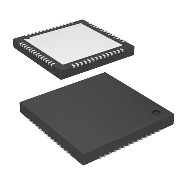


 工商网监
湘ICP备2023018690号
工商网监
湘ICP备2023018690号
