The following document contains information on Cypress products. The document has the series
name, product name, and ordering part numbering with the prefix “MB”. However, Cypress will
offer these products to new and existing customers with the series name, product name, and
ordering part number with the prefix “CY”.
How to Check the Ordering Part Number
1. Go to www.cypress.com/pcn.
2. Enter the keyword (for example, ordering part number) in the SEARCH PCNS field and click
Apply.
3. Click the corresponding title from the search results.
4. Download the Affected Parts List file, which has details of all changes
For More Information
Please contact your local sales office for additional information about Cypress products and
solutions.
About Cypress
Cypress is the leader in advanced embedded system solutions for the world's most innovative
automotive, industrial, smart home appliances, consumer electronics and medical products.
Cypress' microcontrollers, analog ICs, wireless and USB-based connectivity solutions and reliable,
high-performance memories help engineers design differentiated products and get them to market
first. Cypress is committed to providing customers with the best support and development
resources on the planet enabling them to disrupt markets by creating new product categories in
record time. To learn more, go to www.cypress.com.
�MB90387/387S/F387/F387S
MB90V495G
16-bit Microcontrollers
F2MC-16LX MB90385 Series
MB90385 series devices are general-purpose high-performance 16-bit micro controllers designed for process control of consumer
products, which require high-speed real-time processing. The devices of this series have the built-in full-CAN interface.
The system, inheriting the architecture of F2MC family, employs additional instruction ready for high-level languages, expanded
addressing mode, enhanced multiply-divide instructions, and enriched bit-processing instructions. Furthermore, employment of 32bit accumulator achieves processing of long-word data (32 bits).
The peripheral resources of MB90385 series include the following:
8/10-bit A/D converter, UART (SCI), 8/16-bit PPG timer, 16-bit input-output timer (16-bit free-run timer, input capture 0, 1, 2, 3 (ICU)),
and CAN controller.
Features
Clock
■
Time-base timer mode (a mode that operates oscillation clock,
sub clock, time-base timer and watch timer only)
■
Watch mode (a mode that operates sub clock and watch timer
only)
■
Built-in PLL clock frequency multiplication circuit
■
Selection of machine clocks (PLL clocks) is allowed among
frequency division by two on oscillation clock, and multiplication
of 1 to 4 times of oscillation clock (for 4-MHz oscillation clock,
4 MHz to 16 MHz).
■
Stop mode (a mode that stops oscillation clock and sub clock)
■
CPU blocking operation mode
■
Operation by sub-clock (8.192 kHz) is allowed. (MB90387,
MB90F387)
■
■
Minimum execution time of instruction: 62.5 ns (when operating
with 4-MHz oscillation clock, and 4-time multiplied PLL clock).
Process
I/O Port
■
24-bit internal addressing
Instruction System Best Suited to Controller
■
Wide choice of data types (bit, byte, word, and long word)
■
Wide choice of addressing modes (23 types)
■
Enhanced multiply-divide instructions and RETI instructions
■
Enhanced high-precision computing with 32-bit accumulator
Instruction System Compatible with High-level
Language (C language) and Multitask
■
Employing system stack pointer
■
Enhanced various pointer indirect instructions
■
Barrel shift instructions
4-byte instruction queue
Powerful Interrupt Function with 8 Levels and 34
Factors
Automatic Data Transfer Function Independent of CPU
■
Expanded intelligent I/O service function (EI2 OS): Maximum
of 16 channels
Low Power Consumption (standby) Mode
■
Timer
■
Time-base timer, watch timer, watchdog timer: 1 channel
■
8/16-bit PPG timer: 8-bit x 4 channels, or 16-bit x 2 channels
■
16-bit reload timer: 2 channels
■
16-bit input/output timer
❐ 16-bit free run timer: 1 channel
❐ 16-bit input capture: (ICU): 4 channels
Interrupt request is issued upon latching a count value of 16bit free run timer by detection of an edge on pin input.
CAN Controller: 1 channel
Increased Processing Speed
■
General-purpose input/output port (CMOS output):
MB90387, MB90F387: 34 ports (including 4 high-current output ports)
MB90387S, MB90F387S: 36 ports (including 4 high-current
output ports)
16 Mbyte CPU memory Space
■
CMOS technology
■
Compliant with Ver2.0A and Ver2.0B CAN specifications
■
8 built-in message buffers
■
Transmission rate of 10 kbps to 1 Mbps (by 16 MHz machine
clock)
■
CAN wake-up
UART (SCI): 1 channel
■
Equipped with full-duplex double buffer
■
Clock-asynchronous or clock-synchronous serial transmission
is available.
Sleep mode (a mode that halts CPU operating clock)
Cypress Semiconductor Corporation
Document Number: 002-07765 Rev. *A
•
198 Champion Court
•
San Jose, CA 95134-1709
•
408-943-2600
Revised February 5, 2018
�MB90387/387S/F387/F387S
MB90V495G
DTP/External Interrupt: 4 channels, CAN wakeup:
1channel
■
Module for activation of expanded intelligent I/O service
(EI2OS), and generation of external interrupt.
Delay Interrupt Generator Module
■
Generates interrupt request for task switching.
8/10-bit A/D Converter: 8 channels
■
Resolution is selectable between 8-bit and 10-bit.
■
Activation by external trigger input is allowed.
■
Conversion time: 6.125 s (at 16 MHz machine clock, including
sampling time)
Program Patch Function
■
Address matching detection for 2 address pointers.
Document Number: 002-07765 Rev. *A
Page 2 of 81
�MB90387/387S/F387/F387S
MB90V495G
Contents
Product Lineup ...................................................................... 4
Packages And Product Models ............................................ 5
Product Comparison ............................................................. 5
Pin Assignment ..................................................................... 6
Pin Description ...................................................................... 7
I/O Circuit Type ...................................................................... 9
Handling Devices................................................................. 10
Block Diagram ..................................................................... 12
Memory Map......................................................................... 12
Memory Allocation of MB90385 ..................................... 12
Memory Map .................................................................. 13
I/O Map.................................................................................. 14
Interrupt Sources, Interrupt Vectors, And Interrupt Control
Registers .............................................................................. 21
Peripheral Resources..........................................................
I/O Ports .........................................................................
Time-Base Timer............................................................
Watchdog Timer .............................................................
16-bit Input/Output Timer ...............................................
16-bit Reload Timer........................................................
Watch Timer Outline.......................................................
8/16-bit PPG Timer Outline ............................................
Document Number: 002-07765 Rev. *A
22
22
28
30
32
35
37
39
Delay Interrupt Generation Module Outline....................
DTP/External Interrupt and CAN Wakeup Outline .........
8/10-bit A/D Converter....................................................
UART Outline .................................................................
CAN Controller ...............................................................
Address Matching Detection Function Outline ...............
ROM Mirror Function Selection Module Outline.............
512 Kbit Flash Memory Outline ......................................
42
43
45
47
49
51
52
53
Electrical Characteristics....................................................
Absolute Maximum Rating .............................................
Recommended Operating Conditions ............................
DC Characteristics .........................................................
AC Characteristics..........................................................
A/D Converter.................................................................
Definition of A/D Converter Terms .................................
Notes on A/D Converter Section ....................................
Flash Memory Program/Erase Characteristics...............
55
55
57
58
60
67
68
70
70
Example Characteristics..................................................... 71
Ordering Information........................................................... 77
Package Dimension............................................................. 78
Major Changes..................................................................... 79
Document History................................................................ 80
Sales, Solutions, and Legal Information ........................... 81
Page 3 of 81
�MB90387/387S/F387/F387S
MB90V495G
1. Product Lineup
Part Number
Parameter
Classification
MB90F387
MB90F387S
MB90387
MB90387S
MB90V495G
Flash ROM
Mask ROM
Evaluation product
ROM capacity
64 Kbytes
RAM capacity
2 Kbytes
6 Kbytes
Process
CMOS
Package
Operating power supply voltage
LQFP-48 (pin pitch 0.50 mm)
PGA-256
3.5 V to 5.5 V
4.5 V to 5.5 V
None
Special power supply for
emulator*1
CPU functions
Number of basic instructions
Instruction bit length
Instruction length
Data bit length
: 351 instructions
: 8 bits and 16 bits
: 1 byte to 7 bytes
: 1 bit, 8 bits, 16 bits
Minimum instruction execution time: 62.5 ns (at 16 MHz machine clock)
Interrupt processing time: 1.5 s at minimum (at 16 MHz machine clock)
Low power consumption
(standby) mode
Sleep mode / Watch mode / Time-base timer mode / Stop mode / CPU intermittent
I/O port
General-purpose input/output ports (CMOS output): 34 ports (36 ports*2)
including 4 high-current output ports (P14 to P17)
Time-base timer
18-bit free-run counter
Interrupt cycle: 1.024 ms, 4.096 ms, 16.834 ms, 131.072 ms
(with oscillation clock frequency at 4 MHz)
Watchdog timer
Reset generation cycle: 3.58 ms, 14.33 ms, 57.23 ms, 458.75 ms
(with oscillation clock frequency at 4 MHz)
16-bit input/
output timer
16-bit free-run
timer
Number of channels: 1
Interrupt upon occurrence of overflow
Input capture
Number of channels: 4
Retaining free-run timer value set by pin input (rising edge, falling edge, and both edges)
16-bit reload timer
Number of channels: 2
16-bit reload timer operation
Count clock cycle: 0.25 s, 0.5 s, 2.0 s
(at 16-MHz machine clock frequency)
External event count is allowed.
Watch timer
15-bit free-run counter
Interrupt cycle: 31.25 ms, 62.5 ms, 12 ms, 250 ms, 500 ms, 1.0 s, 2.0 s
(with 8.192 kHz sub clock)
8/16-bit PPG timer
Number of channels: 2 (four 8-bit channels are available also.)
PPG operation is allowed with four 8-bit channels or two 16-bit channels.
Outputting pulse wave of arbitrary cycle or arbitrary duty is allowed.
Count clock: 62.5 ns to 1 s
(with 16 MHz machine clock)
Delay interrupt generator module
Interrupt generator module for task switching. Used for realtime OS.
DTP/External interrupt
Number of inputs: 4
Activated by rising edge, falling edge, “H” level or “L” level input.
External interrupt or expanded intelligent I/O service (EI2OS) is available.
Document Number: 002-07765 Rev. *A
Page 4 of 81
�MB90387/387S/F387/F387S
MB90V495G
Part Number
MB90F387
MB90F387S
Parameter
MB90387
MB90387S
MB90V495G
8/10-bit A/D converter
Number of channels: 8
Resolution: Selectable 10-bit or 8-bit.
Conversion time: 6.125 s (at 16 MHz machine clock, including sampling time)
Sequential conversion of two or more successive channels is allowed. (Setting a
maximum of 8 channels is allowed.)
Single conversion mode: Selected channel is converted only once.
Sequential conversion mode: Selected channel is converted repetitively.
Halt conversion mode: Conversion of selected channel is stopped and activated alternately.
UART(SCI)
Number of channels: 1
Clock-synchronous transfer: 62.5 kbps to 2 Mbps
Clock-asynchronous transfer: 9,615 bps to 500 kbps
Communication is allowed by bi-directional serial communication function and master/
slave type connection.
CAN
Compliant with Ver 2.0A and Ver 2.0B CAN specifications.
8 built-in message buffers.
Transmission rate of 10 kbps to 1 Mbps (by 16 MHz machine clock)
CAN wake-up
*1: Settings of DIP switch S2 for using emulation pod MB2145-507. For details, see MB2145-507 Hardware Manual
(2.7 Power Pin solely for Emulator).
*2: MB90387S, MB90F387S
2. Packages And Product Models
Package
MB90F387, MB90F387S
MB90387, MB90387S
LQA048
: Yes : No
Note: Refer to Package Dimension for details of the package.
3. Product Comparison
Memory Space
When testing with test product for evaluation, check the differences between the product and a product to be used actually. Pay
attention to the following points:
■
The MB90V495G has no built-in ROM. However, a special-purpose development tool allows the operations as those of one with
built-in ROM. ROM capacity depends on settings on a development tool.
■
On MB90V495G, an image from FF4000H to FFFFFFH is viewed on 00 bank and an image of FE0000H to FF3FFFH is viewed only
on FE bank and FF bank. (Modified on settings of a development tool.)
■
On MB90F387/F387S/387/387S, an image from FF4000H to FFFFFFH is viewed on 00 bank and an image of FE0000H to FF3FFFH
is viewed only on FF bank.
Document Number: 002-07765 Rev. *A
Page 5 of 81
�MB90387/387S/F387/F387S
MB90V495G
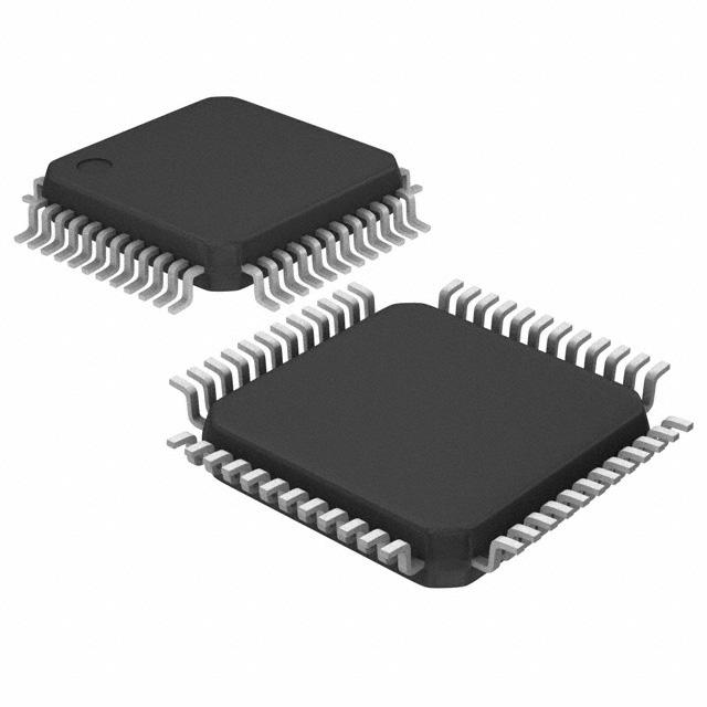
4. Pin Assignment
48
47
46
45
44
43
42
41
40
39
38
37
AVSS
X1A/P36*
X0A/P35*
P33
P32
P31
P30
P44/RX
P43/TX
P42/SOT1
P41/SCK1
P40/SIN1
(Top View)
LQFP-48
13
14
15
16
17
18
19
20
21
22
23
24
1
2
3
4
5
6
7
8
9
10
11
12
36
35
34
33
32
31
30
29
28
27
26
25
P17/PPG3
P16/PPG2
P15/PPG1
P14/PPG0
P13/IN3
P12/IN2
P11/IN1
P10/IN0
X1
X0
C
VSS
P21/TOT0
P22/TIN1
P23/TOT1
P24/INT4
P25/INT5
P26/INT6
P27/INT7
MD2
MD1
MD0
RST
VCC
AVCC
AVR
P50/AN0
P51/AN1
P52/AN2
P53/AN3
P54/AN4
P55/AN5
P56/AN6
P57/AN7
P37/ADTG
P20/TIN0
(LQA048)
*: MB90387, MB90F387
: X1A, X0A
MB90387S, MB90F387S: P36, P35
Document Number: 002-07765 Rev. *A
Page 6 of 81
�MB90387/387S/F387/F387S
MB90V495G
5. Pin Description
Pin No.
Pin Name
Circuit
Type
1
AVcc
Vcc power input pin for A/D converter.
2
AVR
Power (Vref+) input pin for A/D converter. Use as input for Vcc or lower.
3 to 10
P50 to P57
E
General-purpose input/output ports.
AN0 to AN7
11
P37
Functions as analog input pins for A/D converter. Valid when analog input setting is
“enabled.”
D
ADTG
12
P20
P21
D
P22
P23
D
P24 to P27
General-purpose input/output port.
Function as an event input pin for reload timer 1. Use the pin by setting as input port.
D
TOT1
16 to 19
General-purpose input/output port.
Function as an event output pin for reload timer 0. Valid only when output setting is
“enabled.”
TIN1
15
General-purpose input/output port.
Function as an event input pin for reload timer 0. Use the pin by setting as input port.
D
TOT0
14
General-purpose input/output port.
Function as an external trigger input pin for A/D converter. Use the pin by setting as
input port.
TIN0
13
Function
General-purpose input/output port.
Function as an event output pin for reload timer 1. Valid only when output setting is
“enabled.”
D
General-purpose input/output ports.
INT4 to INT7
Functions as external interrupt input pins. Use the pins by setting as input port.
20
MD2
F
Input pin for specifying operation mode. Connect directly to Vss.
21
MD1
C
Input pin for specifying operation mode. Connect directly to Vcc.
22
MD0
C
Input pin for specifying operation mode. Connect directly to Vcc.
23
RST
B
External reset input pin.
24
Vcc
Power source (5 V) input pin.
25
Vss
Power source (0 V) input pin.
26
C
Capacitor pin for stabilizing power source. Connect a ceramic capacitor of approximately 0.1 F.
27
X0
A
Pin for high-rate oscillation.
28
X1
A
Pin for high-rate oscillation.
29 to 32
P10 to P13
D
IN0 to IN3
33 to 36
P14 to P17
G
PPG0 to PPG3
37
P40
P41
General-purpose input/output ports. High-current output ports.
Functions as output pins of PPG timers 01 and 23. Valid when output setting is
“enabled.”
D
SIN1
38
General-purpose input/output ports.
Functions as trigger input pins of input capture ch.0 to ch.3. Use the pins by setting
as input ports.
General-purpose input/output port.
Serial data input pin for UART. Use the pin by setting as input port.
D
SCK1
Document Number: 002-07765 Rev. *A
General-purpose input/output port.
Serial clock input pin for UART. Valid only when serial clock input/output setting on
UART is “enabled.”
Page 7 of 81
�MB90387/387S/F387/F387S
MB90V495G
Pin No.
Pin Name
Circuit
Type
39
P42
D
SOT1
40
P43
Function
General-purpose input/output port.
Serial data input pin for UART. Valid only when serial data input/output setting on
UART is “enabled.”
D
TX
General-purpose input/output port.
Transmission output pin for CAN. Valid only when output setting is “enabled.”
41
P44
D
42 to 45
P30 to P33
D
General-purpose input/output ports.
46
X0A*
A
Pin for low-rate oscillation.
RX
Transmission output pin for CAN. Valid only when output setting is “enabled.”
P35*
47
X1A*
General-purpose input/output port.
A
P36*
48
AVss
*: MB90387, MB90F387:
MB90387S, MB90F387S:
General-purpose input/output port.
Pin for low-rate oscillation.
General-purpose input/output port.
Vss power source input pin for A/D converter.
X1A, X0A
P36, P35
Document Number: 002-07765 Rev. *A
Page 8 of 81
�MB90387/387S/F387/F387S
MB90V495G
6. I/O Circuit Type
Type
Circuit
Remarks
A
X1
Clock input
■
High-rate oscillation feedback resistor,
approx.1 M
■
Low-rate oscillation feedback resistor,
approx.10 M
■
Hysteresis input with pull-up resistor.
X1A
X0
X0A
Standby control signal
B
Vcc
■
Pull-up resistor, approx.50 k
■
Hysteresis input
■
CMOS hysteresis input
■
CMOS level output
■
Standby control provided
■
CMOS hysteresis input
■
CMOS level output
■
Shared for analog input pin
■
Standby control provided
R
R
Hysteresis input
C
R
Hysteresis input
D
Vcc
P-ch
R
N-ch
Vss
Digital output
Digital output
CMOS
hysteresis input
Standby control
E
Vcc
P-ch
R
N-ch
Vss
Digital output
Digital output
CMOS
hysteresis input
Standby control
Analog input
Document Number: 002-07765 Rev. *A
Page 9 of 81
�MB90387/387S/F387/F387S
MB90V495G
Type
Circuit
Remarks
F
R
Hysteresis input
■
Hysteresis input with pull-down resistor
■
Pull-down resistor, approx. 50 k
■
Flash product is not provided with pull-down
resistor.
■
CMOS hysteresis input
■
CMOS level output (high-current output)
■
Standby control provided
R
Vss
G
Vcc
P-ch
High-current output
High-current output
R
N-ch
Vss
CMOS
hysteresis input
Standby control
7. Handling Devices
Do Not Exceed Maximum Rating (preventing “latch up”)
■
On a CMOS IC, latch-up may occur when applying a voltage higher than Vcc or a voltage lower than Vss to input or output pin,
which has no middle or high withstand voltage. Latch-up may also occur when a voltage exceeding maximum rating is applied across
Vcc pin and Vss pin.
■
Latch-up causes drastic increase of power current, which may lead to destruction of elements by heat. Extreme caution must be
taken not to exceed maximum rating.
■
When turning on and off analog power source, take extra care not to apply an analog power voltages (AVcc and AVR) and analog
input voltage that are higher than digital power voltage (Vcc).
Handling Unused Pins
■
Leaving unused input pins open may cause permanent destruction by malfunction or latch-up. Apply pull-up or pull-down process
to the unused pins using resistors of 2 k or higher. Leave unused input/output pins open under output status, or process as input
pins if they are under input status.
Using External Clock
■
When using an external clock, drive only X0 pin and leave X1 pin open. An example of using an external clock is shown below.
Using external clock
X0
Open
X1
MB90385 series
Document Number: 002-07765 Rev. *A
Page 10 of 81
�MB90387/387S/F387/F387S
MB90V495G
Notes When Using No Sub Clock
■
If an oscillator is not connected to X0A and X1A pin, apply pull-down resistor to X0A pin and leave X1A pin open.
About Power Supply Pins
■
If two or more Vcc and Vss pins exist, the pins that should be at the same potential are connected to each other inside the device.
For reducing unwanted emissions and preventing malfunction of strobe signals caused by increase of ground level, however, be
sure to connect the Vcc and Vss pins to the power source and the ground externally.
■
Pay attention to connect a power supply to Vcc and Vss of MB90385 series device in a lowest-possible impedance.
■
Near pins of MB90385 series device, connecting a bypass capacitor is recommended at 0.1 F across Vcc pin and Vss pin.
Crystal Oscillator Circuit
■
Noises around X0 and X1 pins cause malfunctions on a MB90385 series device. Design a print circuit so that X0 and X1 pins, an
crystal oscillator (or a ceramic oscillator), and bypass capacitor to the ground become as close as possible to each other. Furthermore,
avoid wires to X0 and X1 pins crossing each other as much as possible.
■
Print circuit designing that surrounds X0 and X1 pins with grounding wires, which ensures stable operation, is strongly recommended.
Caution on Operations during PLL Clock Mode
■
If the PLL clock mode is selected, the microcontroller attempt to be working with the self-oscillating circuit even when there is no
external oscillator or external clock input is stopped. Performance of this operation, however, cannot be guaranteed.
Sequence of Turning on Power of A/D Converter and Applying Analog Input
■
Be sure to turn on digital power (Vcc) before applying signals to the A/D converter and applying analog input signals (AN0 to AN7 pins).
■
Be sure to turn off the power of A/D converter and analog input before turning off the digital power source.
■
Be sure not to apply AVR exceeding AVcc when turning on and off. (No problems occur if analog and digital power is turned on and
off simultaneously.)
Handling Pins When A/D Converter is Not Used
■
If the A/D converter is not used, connect the pins under the following conditions: “AVcc=AVR=Vcc,” and “AVss=Vss”
Note on Turning on Power
■
For preventing malfunctions on built-in step-down circuit, maintain a minimum of 50 s of voltage rising time (between 0.2 V and
2.7V) when turning on the power.
Stabilization of Supply Voltage
■
A sudden change in the supply voltage may cause the device to malfunction even within the specified VCC supply voltage operating
range. Therefore, the VCC supply voltage should be stabilized.
For reference, the supply voltage should be controlled so that VCC ripple variations (peak-to-peak values) at commercial frequencies
(50 Hz / 60 Hz) fall below 10 of the standard VCC supply voltage and the coefficient of fluctuation does not exceed 0.1 V/ms at
instantaneous power switching.
Document Number: 002-07765 Rev. *A
Page 11 of 81
�MB90387/387S/F387/F387S
MB90V495G
8. Block Diagram
X0,X1
RST
X0A,X1A
Clock
control circuit
CPU
F2MC-16LX core
Watch timer
16-bit
free-run timer
IN0 to IN3
RAM
Input
capture
(4 channels)
16-bit
PPG timer
(2 channels)
PPG0 to PPG3
ROM/Flash
Prescaler
SOT1
SCK1
SIN1
UART1
Internal data bus
Time-base timer
CAN
DTP/External
interrupt
RX
TX
INT4 to INT7
AVcc
AVss
AN0 to AN7
AVR
8/10-bit A/D
converter
(8 channels)
16-bit
reload timer
(2 channels)
TIN0,TIN1
TOT0,TOT1
ADTG
9. Memory Map
MB90385 series allows specifying a memory access mode “single chip mode.”
9.1 Memory Allocation of MB90385
MB90385 series model has 24-bit wide internal address bus and up to 24-bit bus of external address bus.
A maximum of 16-Mbyte memory space of external access memory is accessible.
Document Number: 002-07765 Rev. *A
Page 12 of 81
�MB90387/387S/F387/F387S
MB90V495G
9.2 Memory Map
(with ROM mirroring
function enabled)
000000H
0000C0H
000100H
Peripheral
RAM area
Register
Address #1
003800H
Extension IO
area
004000H
ROM area
(FF bank image)
010000H
FE0000H
ROM area*
FF0000H
ROM area
FFFFFFH
Model
MB90V495G
MB90F387/MB90F387S
MB90387/MB90387S
Address #1
001900H
000900H
000900H
: Internal access memory
: Access disallowed
*: On MB90387/S or MB90F387/S, to read “FE0000H” to “FEFFFFH” is to read out
“FF0000H” to “FFFFFFH”.
Note: When internal ROM is operating, F2MC-16LX allows viewing ROM data image on FF bank at upper-level of 00 bank. This
function is called “mirroring ROM,” which allows effective use of C compiler small model.
F2MC-16LX assigns the same low order 16-bit address to FF bank and 00 bank, which allows referencing table in ROM without
specifying “far” using pointer.
For example, when accessing to “00C000H”, ROM data at “FFC000H” is accessed actually. However, because ROM area of
FF bank exceeds 48 Kbytes, viewing all areas is not possible on 00 bank image. Because ROM data of “FF4000H” to “FFFFFFH”
is viewed on “004000H” to “00FFFFH” image, store a ROM data table in area “FF4000H” to “FFFFFFH.”
Document Number: 002-07765 Rev. *A
Page 13 of 81
�MB90387/387S/F387/F387S
MB90V495G
10. I/O Map
Register
Address Abbreviation
Read/
Write
Register
Resource
Initial Value
(Reserved area) *
000000H
000001H
PDR1
Port 1 data register
R/W
Port 1
XXXXXXXXB
000002H
PDR2
Port 2 data register
R/W
Port 2
XXXXXXXXB
000003H
PDR3
Port 3 data register
R/W
Port 3
XXXXXXXXB
000004H
PDR4
Port 4 data register
R/W
Port 4
XXXXXXXXB
000005H
PDR5
Port 5 data register
R/W
Port 5
XXXXXXXXB
000006H
to
000010H
(Reserved area) *
000011H
DDR1
Port 1 direction data register
R/W
Port 1
00000000B
000012H
DDR2
Port 2 direction data register
R/W
Port 2
00000000B
000013H
DDR3
Port 3 direction data register
R/W
Port 3
000X0000B
000014H
DDR4
Port 4 direction data register
R/W
Port 4
XXX00000B
000015H
DDR5
Port 5 direction data register
R/W
Port 5
00000000B
8/10-bit A/D
converter
11111111B
UART1
00000000B
000016H
to
00001AH
00001BH
(Reserved area) *
ADER
Analog input permission register
00001CH to
000025H
R/W
(Reserved area) *
000026H
SMR1
Serial mode register 1
R/W
000027H
SCR1
Serial control register 1
R/W, W
00000100B
000028H
SIDR1/
SODR1
R, W
XXXXXXXXB
000029H
SSR1
R, R/W
00001000B
Serial input data register 1/ Serial output
data register 1
Serial status data register 1
00002AH
00002BH
(Reserved area) *
CDCR1
Communication prescaler control
register 1
00002CH to
00002FH
R/W
UART1
0XXX0000B
DTP/External
interrupt
00000000B
(Reserved area) *
000030H
ENIR
DTP/External interrupt permission
register
R/W
000031H
EIRR
DTP/External interrupt permission
register
R/W
XXXXXXXXB
000032H
ELVR
Detection level setting register
R/W
00000000B
ADCS
A/D control status register
000033H
000034H
R/W
000035H
000036H
R/W
R/W, W
ADCR
A/D data register
000037H
Document Number: 002-07765 Rev. *A
00000000B
8/10-bit A/D
converter
00000000B
00000000B
W, R
XXXXXXXXB
R
00101XXXB
Page 14 of 81
�MB90387/387S/F387/F387S
MB90V495G
Register
Address Abbreviation
Read/
Write
Register
000038H
to
00003FH
PPGC0
PPG0 operation mode control register
R/W, W
000041H
PPGC1
PPG1 operation mode control register
R/W, W
000042H
PPG01
PPG0/1 count clock selection register
R/W
000043H
8/16-bit PPG timer 0/
1
0X000XX1B
PPGC2
PPG2 operation mode control register
R/W, W
000045H
PPGC3
PPG3 operation mode control register
R/W, W
000046H
PPG23
PPG2/3 count clock selection register
R/W
000047H to
00004FH
000000XXB
8/16-bit PPG timer 2/
3
IPCP0
IPCP1
Input capture data register 0
R
Input capture data register 1
16-bit input/output
timer
R
ICS01
000055H
ICS23
000056H
TCDT
Input capture control status register
R/W
00000000B
00000000B
Timer counter data register
R/W
00000000B
00000000B
TCCS
Timer counter control status register
000059H
R/W
00000000B
(Reserved area) *
IPCP2
Input capture data register 2
R
00005BH
IPCP3
Input capture data register 3
16-bit input/output
timer
R
(Reserved area) *
TMCSR0
Timer control status register
R/W
000067H
TMCSR1
R/W
000069H
00000000B
XXXX0000B
16-bit reload timer 1
R/W
00000000B
XXXX0000B
(Reserved area) *
ROMM
ROM mirroring function selection register
000070H
to
00007FH
W
ROM mirroring
function selection
module
XXXXXXX1B
(Reserved area) *
BVALR
Message buffer enabling register
000081H
000082H
16-bit reload timer 0
R/W
00006AH to
00006EH
000080H
XXXXXXXXB
XXXXXXXXB
00005EH to
000065H
00006FH
XXXXXXXXB
XXXXXXXXB
00005DH
000068H
XXXXXXXXB
XXXXXXXXB
000057H
000066H
XXXXXXXXB
XXXXXXXXB
000054H
00005CH
0X000001B
000000XXB
000053H
00005AH
0X000XX1B
(Reserved area) *
000051H
000058H
0X000001B
(Reserved area) *
000044H
000052H
Initial Value
(Reserved area) *
000040H
000050H
Resource
R/W
CAN controller
00000000B
CAN controller
00000000B
(Reserved area) *
TREQR
Send request register
Document Number: 002-07765 Rev. *A
R/W
Page 15 of 81
�MB90387/387S/F387/F387S
MB90V495G
Register
Address Abbreviation
000083H
000084H
TCANR
Send cancel register
TCR
RCR
R/W
Receive completion register
00000000B
CAN controller
00000000B
R/W
CAN controller
00000000B
CAN controller
00000000B
CAN controller
00000000B
CAN controller
00000000B
(Reserved area) *
RRTRR
Receive RTR register
R/W
(Reserved area) *
ROVRR
Receive overrun register
00008DH
00008EH
CAN controller
(Reserved area) *
00008BH
00008CH
W
Send completion register
000089H
00008AH
Initial Value
(Reserved area) *
000087H
000088H
Resource
(Reserved area) *
000085H
000086H
Read/
Write
Register
R/W
(Reserved area) *
RIER
Receive completion interrupt
permission register
00008FH
to
00009DH
R/W
(Reserved area) *
00009EH
PACSR
Address detection control register
R/W
Address matching
detection function
00000000B
00009FH
DIRR
Delay interrupt request generation/
release register
R/W
Delay interrupt
generation module
XXXXXXX0B
0000A0H
LPMCR
Lower power consumption mode control
register
W,R/W
Lower power
consumption mode
00011000B
0000A1H
CKSCR
Clock selection register
R,R/W
Clock
11111100B
0000A2H
to
0000A7H
(Reserved area) *
0000A8H
WDTC
Watchdog timer control register
R,W
0000A9H
TBTC
Time-base timer control register
0000AAH
WTC
Watch timer control register
0000ABH
to
0000ADH
0000AEH
Watchdog timer
XXXXX111B
R/W,W
Time-base timer
1XX00100B
R,R/W
Watch timer
1X001000B
(Reserved area) *
FMCS
Flash memory control status register
0000AFH
Document Number: 002-07765 Rev. *A
R,W,R/W 512k-bit Flash
memory
000X0000B
(Reserved area) *
Page 16 of 81
�MB90387/387S/F387/F387S
MB90V495G
Register
Address Abbreviation
Read/
Write
Register
R/W
Resource
Interrupt controller
Initial Value
0000B0H
ICR00
Interrupt control register 00
00000111B
0000B1H
ICR01
Interrupt control register 01
00000111B
0000B2H
ICR02
Interrupt control register 02
00000111B
0000B3H
ICR03
Interrupt control register 03
00000111B
0000B4H
ICR04
Interrupt control register 04
00000111B
0000B5H
ICR05
Interrupt control register 05
00000111B
0000B6H
ICR06
Interrupt control register 06
00000111B
0000B7H
ICR07
Interrupt control register 07
00000111B
0000B8H
ICR08
Interrupt control register 08
00000111B
0000B9H
ICR09
Interrupt control register 09
00000111B
0000BAH
ICR10
Interrupt control register 10
00000111B
0000BBH
ICR11
Interrupt control register 11
00000111B
0000BCH
ICR12
Interrupt control register 12
00000111B
0000BDH
ICR13
Interrupt control register 13
00000111B
0000BEH
ICR14
Interrupt control register 14
00000111B
0000BFH
ICR15
Interrupt control register 15
0000C0H
to
0000FFH
001FF0H
00000111B
(Reserved area) *
PADR0
Detection address setting register 0
(low-order)
R/W
Address matching
detection function
XXXXXXXXB
001FF1H
Detection address setting register 0
(middle-order)
XXXXXXXXB
001FF2H
Detection address setting register 0
(high-order)
XXXXXXXXB
001FF3H
PADR1
Detection address setting register 1
(low-order)
R/W
XXXXXXXXB
001FF4H
Detection address setting register 1
(middle-order)
XXXXXXXXB
001FF5H
Detection address setting register 1
(high-order)
XXXXXXXXB
003900H
003901H
003902H
003903H
TMR0/
TMRLR0
16-bit timer register 0/16-bit reload
register
R,W
TMR1/
TMRLR1
16-bit timer register 1/16-bit reload
register
R,W
003904H
to
00390FH
Document Number: 002-07765 Rev. *A
16-bit reload timer 0
XXXXXXXXB
XXXXXXXXB
16-bit reload timer 1
XXXXXXXXB
XXXXXXXXB
(Reserved area) *
Page 17 of 81
�MB90387/387S/F387/F387S
MB90V495G
Register
Address Abbreviation
Register
Read/
Write
Resource
8/16-bit PPG timer
Initial Value
003910H
PRLL0
PPG0 reload register L
R/W
003911H
PRLH0
PPG0 reload register H
R/W
XXXXXXXXB
003912H
PRLL1
PPG1 reload register L
R/W
XXXXXXXXB
003913H
PRLH1
PPG1 reload register H
R/W
XXXXXXXXB
003914H
PRLL2
PPG2 reload register L
R/W
XXXXXXXXB
003915H
PRLH2
PPG2 reload register H
R/W
XXXXXXXXB
003916H
PRLL3
PPG3 reload register L
R/W
XXXXXXXXB
003917H
PRLH3
PPG3 reload register H
R/W
XXXXXXXXB
003918H
to
00392FH
(Reserved area) *
003930H
to
003BFFH
(Reserved area) *
003C00H
to
003C0FH
RAM (General-purpose RAM)
XXXXXXXXB
003C10H
to
003C13H
IDR0
ID register 0
R/W
003C14H
to
003C17H
IDR1
ID register 1
R/W
XXXXXXXXB
to
XXXXXXXXB
003C18H
to
003C1BH
IDR2
ID register 2
R/W
XXXXXXXXB
to
XXXXXXXXB
003C1CH
to
003C1FH
IDR3
ID register 3
R/W
XXXXXXXXB
to
XXXXXXXXB
003C20H
to
003C23H
IDR4
ID register 4
R/W
XXXXXXXXB
to
XXXXXXXXB
003C24H
to
003C27H
IDR5
ID register 5
R/W
XXXXXXXXB
to
XXXXXXXXB
003C28H
to
003C2BH
IDR6
ID register 6
R/W
XXXXXXXXB
to
XXXXXXXXB
003C2CH
to
003C2FH
IDR7
ID register 7
R/W
XXXXXXXXB
to
XXXXXXXXB
003C30H,
003C31H
DLCR0
DLC register 0
R/W
XXXXXXXXB,
XXXXXXXXB
003C32H,
003C33H
DLCR1
DLC register 1
R/W
XXXXXXXXB,
XXXXXXXXB
003C34H,
003C35H
DLCR2
DLC register 2
R/W
XXXXXXXXB,
XXXXXXXXB
003C36H,
003C37H
DLCR3
DLC register 3
R/W
XXXXXXXXB,
XXXXXXXXB
Document Number: 002-07765 Rev. *A
CAN controller
XXXXXXXXB
to
XXXXXXXXB
Page 18 of 81
�MB90387/387S/F387/F387S
MB90V495G
Register
Address Abbreviation
Read/
Write
Register
Resource
003C38H,
003C39H
DLCR4
DLC register 4
R/W
003C3AH,
003C3BH
DLCR5
DLC register 5
R/W
XXXXXXXXB,
XXXXXXXXB
003C3CH,
003C3DH
DLCR6
DLC register 6
R/W
XXXXXXXXB,
XXXXXXXXB
003C3EH,
003C3FH
DLCR7
DLC register 7
R/W
XXXXXXXXB,
XXXXXXXXB
003C40H
to
003C47H
DTR0
Data register 0
R/W
XXXXXXXXB
to
XXXXXXXXB
003C48H
to
003C4FH
DTR1
Data register 1
R/W
XXXXXXXXB
to
XXXXXXXXB
003C50H
to
003C57H
DTR2
Data register 2
R/W
XXXXXXXXB
to
XXXXXXXXB
003C58H
to
003C5FH
DTR3
Data register 3
R/W
XXXXXXXXB
to
XXXXXXXXB
003C60H
to
003C67H
DTR4
Data register 4
R/W
XXXXXXXXB
to
XXXXXXXXB
003C68H
to
003C6FH
DTR5
Data register 5
R/W
XXXXXXXXB
to
XXXXXXXXB
003C70H
to
003C77H
DTR6
Data register 6
R/W
XXXXXXXXB
to
XXXXXXXXB
003C78H
to
003C7FH
DTR7
Data register 7
R/W
XXXXXXXXB
to
XXXXXXXXB
003C80H
to
003CFFH
CAN controller
Initial Value
XXXXXXXXB,
XXXXXXXXB
(Reserved area) *
003D00H,
003D01H
CSR
Control status register
003D02H
LEIR
Last event display register
003D03H
R/W, R
CAN controller
R/W
0XXXX001B,
00XXX000B
000XX000B
(Reserved area) *
003D04H,
003D05H
RTEC
Send/receive error counter
003D06H,
003D07H
BTR
Bit timing register
R/W
11111111B,
X1111111B
003D08H
IDER
IDE register
R/W
XXXXXXXXB
003D09H
003D0AH
CAN controller
00000000B,
00000000B
(Reserved area) *
TRTRR
Send RTR register
RFWTR
Remote frame receive wait register
003D0BH
003D0CH
R
R/W
CAN controller
00000000B
CAN controller
XXXXXXXXB
(Reserved area) *
Document Number: 002-07765 Rev. *A
R/W
Page 19 of 81
�MB90387/387S/F387/F387S
MB90V495G
Register
Address Abbreviation
003D0DH
003D0EH
Resource
Initial Value
(Reserved area) *
TIER
Send completion interrupt permission
register
003D0FH
003D10H,
003D11H
Read/
Write
Register
R/W
CAN controller
00000000B
CAN controller
XXXXXXXXB,
XXXXXXXXB
CAN controller
XXXXXXXXB
to
XXXXXXXXB
(Reserved area) *
AMSR
Acceptance mask selection register
003D12H,
003D13H
R/W
(Reserved area) *
003D14H
to
003D17H
AMR0
Acceptance mask register 0
R/W
003D18H
to
003D1BH
AMR1
Acceptance mask register 1
R/W
003D1CH
to
003DFFH
(Reserved area) *
003E00H
to
003EFFH
(Reserved area) *
003FF0H
to
003FFFH
(Reserved area) *
XXXXXXXXB
to
XXXXXXXXB
Initial values:
0: Initial value of this bit is “0.”
1: Initial value of this bit is “1.”
X: Initial value of this bit is undefined.
*: “Reserved area” should not be written anything. Result of reading from “Reserved area” is undefined.
Document Number: 002-07765 Rev. *A
Page 20 of 81
�MB90387/387S/F387/F387S
MB90V495G
11. Interrupt Sources, Interrupt Vectors, And Interrupt Control Registers
Interrupt Source
EI2OS
Readiness
Interrupt Vector
Number
Interrupt Control Register
ICR
Address
08H
FFFFDCH
High
Reset
#08
INT 9 instruction
#09
09H
FFFFD8H
Exceptional treatment
#10
0AH
FFFFD4H
CAN controller reception completed
(RX)
´
#11
0BH
FFFFD0H
ICR00
0000B0H*1
CAN controller transmission
completed (TX) / Node status
transition (NS)
´
#12
0CH
FFFFCCH
Reserved
#13
0DH
FFFFC8H
ICR01
0000B1H
Reserved
#14
0EH
FFFFC4H
CAN wakeup
#15
0FH
FFFFC0H
ICR02
0000B2H*1
Time-base timer
#16
10H
FFFFBCH
#17
11H
FFFFB8H
ICR03
0000B3H*1
#18
12H
FFFFB4H
#19
13H
FFFFB0H
ICR04
0000B4H*1
ICR05
0000B5H*1
ICR06
0000B6H*1
ICR07
0000B7H*2
ICR08
0000B8H*1
ICR09
0000B9H*1
ICR10
0000BAH*1
ICR11
0000BBH*1
ICR12
0000BCH*1
16-bit free-run timer overflow
Reserved
#20
14H
FFFFACH
Reserved
#21
15H
FFFFA8H
PPG timer ch0, ch1 underflow
´
#22
16H
FFFFA4H
Input capture 0-input
#23
17H
FFFFA0H
#24
18H
FFFF9CH
Input capture 1-input
#25
19H
FFFF98H
PPG timer ch2, ch3 underflow
´
#26
1AH
FFFF94H
External interrupt (INT6/INT7)
#27
1BH
FFFF90H
Watch timer
#28
1CH
FFFF8CH
Reserved
#29
1DH
FFFF88H
´
#30
1EH
FFFF84H
Reserved
#31
1FH
FFFF80H
Reserved
#32
20H
FFFF7CH
Reserved
#33
21H
FFFF78H
Reserved
#34
22H
FFFF74H
Reserved
#35
23H
FFFF70H
#36
24H
FFFF6CH
16-bit reload timer 0
8/10-bit A/D converter
External interrupt (INT4/INT5)
Input capture 2-input
Input capture 3-input
16-bit reload timer 1
Document Number: 002-07765 Rev. *A
Priority*3
Address
Low
Page 21 of 81
�MB90387/387S/F387/F387S
MB90V495G
Interrupt Source
EI2OS
Readiness
UART1 reception completed
Interrupt Vector
Number
Interrupt Control Register
Address
ICR
Address
ICR13
0000BDH*1
ICR14
1
0000BEH*
ICR15
0000BFH*1
#37
25H
FFFF68H
#38
26H
FFFF64H
UART1 transmission completed
Reserved
#39
27H
FFFF60H
Reserved
#40
28H
FFFF5CH
Flash memory
#41
29H
FFFF58H
Delay interrupt generation module
#42
2AH
FFFF54H
Priority*3
High
Low
: Available
: Unavailable
: Available El2OS function is provided.
: Available when a cause of interrupt sharing a same ICR is not used.
*1:
❐
Peripheral functions sharing an ICR register have the same interrupt level.
If peripheral functions share an ICR register, only one function is available when using expanded intelligent I/O service.
❐ If peripheral functions share an ICR register, a function using expanded intelligent I/O service does not allow interrupt by another
function.
*2: Input capture 1 corresponds to EI2OS, however, PPG does not. When using EI2OS by input capture 1, interrupt should be disabled
for PPG.
❐
*3:Priority when two or more interrupts of a same level occur simultaneously.
12. Peripheral Resources
12.1 I/O Ports
The I/O ports are used as general-purpose input/output ports (parallel I/O ports). The MB60385 series model is provided with 5 ports
(34 inputs). The ports function as input/output pins for peripheral functions also.
I/O Port Functions
An I/O port, using port data resister (PDR), outputs the output data to I/O pin and input a signal input to I/O port. The port direction
register (DDR) specifies direction of input/output of I/O pins on a bit-by-bit basis.
The following summarizes functions of the ports and sharing peripheral functions:
■
Port 1: General-purpose input/output port, used also for PPG timer output and input capture inputs.
■
Port 2: General-purpose input/output port, used also for reload timer input/output and external interrupt input.
■
Port 3: General-purpose input/output port, used also for A/D converter activation trigger pin.
■
Port 4: General-purpose input/output port, used also for UART input/output and CAN controller send/receive pin.
■
Port 5: General-purpose input/output port, used also analog input pin.
Document Number: 002-07765 Rev. *A
Page 22 of 81
�MB90387/387S/F387/F387S
MB90V495G
Port 1 Pins Block Diagram (single-chip mode)
Peripheral
function input
Peripheral
function output
Peripheral function
output permission
Port data register (PDR)
PDR read
Internal data bus
P-ch
Output latch
PDR write
Pin
Port direction register (DDR)
Direction
latch
N-ch
DDR write
Standby control (SPL=1)
DDR read
Standby control: Control among Stop mode (SPL=1), Time-base timer mode (SPL=1), and watch mode
(SPL=1).
Port 1 Registers (single-chip mode)
■
Port 1 registers include port 1 data register (PDR1) and port 1 direction register (DDR1).
■
The bits configuring the register correspond to port 1 pins on a one-to-one basis.
Relation between Port 1 Registers and Pins
Port Name
Port 1
Bits of Register and Corresponding Pins
PDR1, DDR1
bit7
bit6
bit5
bit4
bit3
bit2
bit1
bit0
Corresponding pins
P17
P16
P15
P14
P13
P12
P11
P10
Document Number: 002-07765 Rev. *A
Page 23 of 81
�MB90387/387S/F387/F387S
MB90V495G
Port 2 Pins Block Diagram (general-purpose input/output port)
Peripheral
function input
Peripheral
function output
Peripheral function
output permission
Port data register (PDR)
PDR read
Internal data bus
Output latch
P-ch
PDR write
Pin
Port direction register (DDR)
Direction
latch
N-ch
DDR write
Standby control (SPL=1)
DDR read
Standby control: Control among Stop mode (SPL=1), Time-base timer mode (SPL=1), and watch mode
(SPL=1).
Port 2 Registers
■
Port 2 registers include port 2 data register (PDR2) and port 2 direction register (DDR2).
■
The bits configuring the register correspond to port 2 pins on a one-to-one basis.
Relation between Port 2 Registers and Pins
Port Name
Port 2
Bits of Register and Corresponding Pins
PDR2,DDR2
bit7
bit6
bit5
bit4
bit3
bit2
bit1
bit0
Corresponding pins
P27
P26
P25
P24
P23
P22
P21
P20
Document Number: 002-07765 Rev. *A
Page 24 of 81
�MB90387/387S/F387/F387S
MB90V495G
Port 3 Pins Block Diagram (general-purpose input/output port)
Peripheral
function input
Peripheral
function output
Peripheral function
output permission
Port data register (PDR)
PDR read
Internal data bus
P-ch
Output latch
PDR write
Pin
Port direction register (DDR)
N-ch
Direction
latch
DDR write
Standby control (SPL=1)
DDR read
Standby control: Control among Stop mode (SPL=1), Time-base timer mode (SPL=1), and watch mode
(SPL=1).
Port 3 Registers
■
Port 3 registers include port 3 data register (PDR3) and port 3 direction register (DDR3).
■
The bits configuring the register correspond to port 3 pins on a one-to-one basis.
Relation between Port 3 Registers and Pins
Port Name
Port 3
Bits of Register and Corresponding Pins
PDR3, DDR3
bit7
bit6
bit5
bit4
bit3
bit2
bit1
bit0
Corresponding pins
P37
P36*
P35*
P33
P32
P31
P30
*: P35 and P36 do not exist on MB90387and MB90F387.
Document Number: 002-07765 Rev. *A
Page 25 of 81
�MB90387/387S/F387/F387S
MB90V495G
Port 4 Pins Block Diagram
Peripheral
function input
Peripheral
function output
Peripheral function
output permission
Port data register (PDR)
PDR read
Internal data bus
P-ch
Output latch
PDR write
Pin
Port direction register (DDR)
Direction
latch
N-ch
DDR write
Standby control (SPL=1)
DDR read
Standby control: Control among Stop mode (SPL=1), Time-base timer mode (SPL=1), and watch mode
(SPL=1).
Port 4 Registers
■
Port 4 registers include port 4 data register (PDR4) and port 4 direction register (DDR4).
■
The bits configuring the register correspond to port 4 pins on a one-to-one basis.
Relation between Port 4 Registers and Pins
Port Name
Port 4
Bits of Register and Corresponding Pins
PDR4, DDR4
bit4
bit3
bit2
bit1
bit0
Corresponding pins
P44
P43
P42
P41
P40
Document Number: 002-07765 Rev. *A
Page 26 of 81
�MB90387/387S/F387/F387S
MB90V495G
Port 5 Pins Block Diagram
Analog input
ADER
Port data register (PDR)
PDR read
Internal data bus
Output latch
P-ch
PDR write
Pin
Port direction register (DDR)
Direction
latch
N-ch
DDR write
Standby control (SPL=1)
DDR read
Standby control: Control among Stop mode (SPL=1), Time-base timer mode (SPL=1), and watch mode
(SPL=1).
Port 5 Registers
■
Port 5 registers include port 5 data register (PDR5), port 5 direction register (DDR5), and analog input permission register (ADER).
■
Analog input permission register (ADER) allows or disallows input of analog signal to the analog input pin.
■
The bits configuring the register correspond to port 5 pins on a one-to-one basis.
Relation between Port 5 Registers and Pins
Port Name
Port 5
Bits of Register and Corresponding Pins
PDR5, DDR5
ADER
Corresponding pins
Document Number: 002-07765 Rev. *A
bit7
bit6
bit5
bit4
bit3
bit2
bit1
bit0
ADE7
ADE6
ADE5
ADE4
ADE3
ADE2
ADE1
ADE0
P57
P56
P55
P54
P53
P52
P51
P50
Page 27 of 81
�MB90387/387S/F387/F387S
MB90V495G
12.2 Time-Base Timer
The time-base time is an 18-bit free-run counter (time-base timer counter) that counts up in synchronization with the main clock
(dividing main oscillation clock by 2).
■
Four choices of interval time are selectable, and generation of interrupt request is allowed for each interval time.
■
Provides operation clock signal to oscillation stabilizing wait timer and peripheral functions.
Interval Timer Function
■
When the counter of time-base timer reaches an interval time specified by interval time selection bit (TBTC:TBC1, TBC0), an overflow
(carrying-over) occurs (TBTC: TBOF=1) and interrupt request is generated.
■
If an interrupt by overflow is permitted (TBTC: TBIE=1), an interrupt is generated when overflow occurs (TBTC: TBOF=1).
■
The following four interval time settings are selectable:
Interval Time of Time-base Timer
Count Clock
2/HCLK (0.5 s)
Interval Time
12
2 /HCLK (Approx. 1.0 ms)
214/HCLK (Approx. 4.1 ms)
216/HCLK (Approx. 16.4 ms)
219/HCLK (Approx. 131.1 ms)
HCLK: Oscillation clock
Values in parentheses “( )” are those under operation of 4-MHz oscillation clock.
Document Number: 002-07765 Rev. *A
Page 28 of 81
�MB90387/387S/F387/F387S
MB90V495G
Time-base Timer Block Diagram
To watchdog
timer
To PPG timer
Time-base timer counter
21/HCLK
×21 ×22 ×23 · · ·
···
×28 ×29 ×210 ×211 ×212 ×213 ×214 ×215 ×216 ×217 ×218
OF
OF
OF
OF
Power-on reset
Stop mode
CKSCR : MCS = 1
CKSCR : SCS = 0
0*1
1*2
To clock controller
oscillation stabilizing
wait time selector
Counterclear circuit
Interval timer
selector
TBOF clear TBOF set
Time-base timer control register Re(TBTC) served
-
-
TBIE TBOF TBR TBC1 TBC0
Time-base timer interrupt signal
OF : Overflow
HCLK : Oscillation clock
*1: Switch machine clock from main clock to PLL clock.
*2: Switch machine clock from sub clock to main clock.
Actual interrupt request number of time-base timer is as follows:
Interrupt request number: #16 (10H)
Document Number: 002-07765 Rev. *A
Page 29 of 81
�MB90387/387S/F387/F387S
MB90V495G
12.3 Watchdog Timer
The watchdog timer is a 2-bit counter that uses time-base timer or watch timer as count clock. If the counter is not cleared within an
interval time, CPU is reset.
Watchdog Timer Functions
■
The watchdog timer is a timer counter that prevents runaway of a program. Once a watchdog timer is activated, the counter of
watchdog timer must always be cleared within a specified time of interval. If specified interval time elapses without clearing the
counter of a watchdog timer, CPU resetting occurs. This is the function of a watchdog timer.
■
The interval time of a watchdog timer is determined by a clock cycle, which is input as a count clock. Watchdog resetting occurs
between a minimum time and a maximum time specified.
■
The output target of a clock source is specified by the watchdog clock selection bit (WTC: WDCS) in the watch timer control register.
■
Interval time of a watchdog timer is specified by the time-base timer output selection bit / watch timer output selection bit (WDTC:
WT1, WT0) in the watchdog timer control register.
Interval Timer of Watchdog Timer
Min
Max
Clock Cycle
Min
Max
Clock Cycle
Approx. 3.58 ms
Approx. 4.61 ms
(2 2 )
/HCLK
Approx. 0.457 s
Approx. 0.576 s
(21229)
/SCLK
Approx. 14.33 ms
Approx. 18.3 ms
(216213)
/HCLK
Approx. 3.584 s
Approx. 4.608 s
(215212)
/SCLK
Approx. 57.23 ms
Approx. 73.73 ms
(218215)
/HCLK
Approx. 7.168 s
Approx. 9.216 s
(216213)
/SCLK
Approx.
458.75 ms
Approx.
589.82 ms
(221218)
/HCLK
Approx.
14.336 s
Approx.
18.432 s
(217214)
/SCLK
14
11
HCLK: Oscillation clock (4 MHz), CSCLK: Sub clock (8.192 kHz)
Notes:
■
If the time-base timer is cleared when watchdog timer count clock is used as time base timer output (carry-over signal), watchdog
reset time may become longer.
■
When using the sub clock as machine clock, be sure to specify watchdog timer clock source selection bit (WDCS) in watch timer
control register (WTC) at “0,” selecting output of watch timer.
Document Number: 002-07765 Rev. *A
Page 30 of 81
�MB90387/387S/F387/F387S
MB90V495G
Watchdog Timer Block Diagram
Watch timer control register (WTC)
Watchdog timer control register(WDTC)
WRST ERST SRST WTE WT1 WT0
PONR
Watchdog timer
WDCS
2
Activate
Reset occurs
Shift to sleep mode
Shift to time-base
timer mode
Shift to watch mode
Shift to stop mode
Counter
clear control
circuit
Watchdog
reset
generation
circuit
2-bit
counter
Count clock
selector
Internal reset
generation
circuit
Clear
4
4
Time-base timer counter
Main clock
(dividing HCLK by 2)
21
22
28
29
210
25
26
27
211 212
213
214
215
216
217
218
28
210
211
212 213
214
215
Watch counter
Sub clock
SCLK
21
22
29
HCLK: Oscillation clock
SCLK: Sub clock
Document Number: 002-07765 Rev. *A
Page 31 of 81
�MB90387/387S/F387/F387S
MB90V495G
12.4 16-bit Input/Output Timer
The 16-bit input/output timer is a compound module composed of 16-bit free-run timer, (1 unit) and input capture (2 units, 4 input pins).
The timer, using the 16-bit free-run timer as a basis, enables measurement of clock cycle of an input signal and its pulse width.
Configuration of 16-bit Input/Output Timer
The 16-bit input/output timer is composed of the following modules:
■
16-bit free-run timer (1 unit)
■
Input capture (2 units, 2 input pins per unit)
Functions of 16-bit Input/Output Timer
Functions of 16-bit Free-run Timer
The 16-bit free-run timer is composed of 16-bit up counter, timer counter control status register, and prescaler. The 16-bit up counter
increments in synchronization with dividing ratio of machine clock.
■
Count clock is set among four types of machine clock dividing rates.
■
Generation of interrupt is allowed by counter value overflow.
■
Activation of expanded intelligent I/O service (EI2OS) is allowed by interrupt generation.
■
Counter value of 16-bit free-run timer is cleared to “0000H” by either resetting or software-clearing with timer count clear bit (TCCS:
CLR).
■
Counter value of 16-bit free-run timer is output to input capture, which is available as base time for capture operation.
Functions of Input Capture
The input capture, upon detecting an edge of a signal input to the input pin from external device, stores a counter value of 16-bit freerun timer at the time of detection into the input capture data register. The function includes the input capture data registers corresponding to four input pins, input capture control status register, and edge detection circuit.
■
Rising edge, falling edge, and both edges are selectable for detection.
■
Generating interrupt on CPU is allowed by detecting an edge of input signal.
■
Expanded intelligent I/O service (EI2OS) is activated by interrupt generation.
■
The four input capture input pins and input capture data registers allows monitoring of a maximum of four events.
16-bit Input/Output Timer Block Diagram
Internal data bus
Input capture
Document Number: 002-07765 Rev. *A
Specialpurpose bus
16-bit free-run
timer
Page 32 of 81
�MB90387/387S/F387/F387S
MB90V495G
16-bit Free-run Timer
Counter value of 16-bit free-run timer is used as reference time (base time) of input capture.
Input Capture
Input capture detects rising edge, falling edge or both edges and retains a counter value of 16-bit free-run timer. Detection of edge
on input signal is allowed to generate interrupt.
16-bit Free-run Timer Block Diagram
Timer counter data register
(TCDT)
Output counter value
to input capture
16-bit free-run timer
OF
STOP
CLK
CLR
Internal data bus
Prescaler
2
Timer counter
control status register
(TCCS)
IVF
IVFE STOP
Reserved
CLR CLK2 CLK1 CLK0
: Machine clock
OF: Overflow
Free-run timer
interrupt request
Detailed Pin Assignment on Block Diagram
The 16-bit input/output timer includes a 16-bit free-run timer. Interrupt request number of the 16-bit free-run timer is as follows:
Interrupt request number: 19 (13H)
Prescaler
The prescaler divides a machine clock and provides a counter clock to the 16-bit up counter. Dividing ratio of the machine clock is
specified by timer counter control status register (TCCS) among four values.
Timer Counter Data Register (TCDT)
The timer counter data register is a 16-bit up counter. A current counter value of the 16-bit free-run timer is read. Writing a value during
halt of the counter allows setting an arbitrary counter value.
Document Number: 002-07765 Rev. *A
Page 33 of 81
�MB90387/387S/F387/F387S
MB90V495G
Input Capture Block Diagram
16-bit free-run timer
Edge detection
circuit
IN3
Input capture data register 3 (IPCP3)
Pin
IN2
Input capture data register 2 (IPCP2)
Pin
2
2
Input capture control
status register
(ICS23)
ICP1 ICP0 ICE1 ICE0 EG11 EG10 EG01 EG00
Internal data bus
Input capture
interrupt request
Input capture control
ICP1 ICP0 ICE1 ICE0 EG11 EG10 EG01 EG00
status register
(ICS01)
2
2
IN1
Pin
Input capture data register 1 (IPCP1)
IN0
Input capture data register 0 (IPCP0)
Pin
Edge detection
circuit
Document Number: 002-07765 Rev. *A
Page 34 of 81
�MB90387/387S/F387/F387S
MB90V495G
12.5 16-bit Reload Timer
The 16-bit reload timer has the following functions:
■
Count clock is selectable among 3 internal clocks and external event clock.
■
Activation trigger is selectable between software trigger and external trigger.
■
Generation of CPU interrupt is allowed upon occurrence of underflow on 16-bit timer register. Available as an interval timer using
the interrupt function.
■
When underflow of 16-bit timer register (TMR) occurs, one of two reload modes is selectable between one-shot mode that halts
counting operation of TMR, and reload mode that reloads 16-bit reload register value to TMR, continuing TMR counting operation.
■
The 16-bit reload timer is ready for expanded intelligent I/O service (EI2OS).
■
MB90385 series device has 2 channels of built-in 16-bit reload timer.
Operation Mode of 16-bit Reload Timer
Count Clock
Activation Trigger
Operation upon Underflow
Internal clock mode
Software trigger, external trigger
One-shot mode, reload mode
Event count mode
Software trigger
One-shot mode, reload mode
Internal Clock Mode
■
The 16-bit reload timer is set to internal clock mode, by setting count clock selection bit (TMCSR: CSL1, CSL0) to “00B”, “01B”, “10B”.
■
In the internal clock mode, the counter decrements in synchronization with the internal clock.
■
Three types of count clock cycles are selectable by count clock selection bit (TMCSR: CSL1, CSL0) in timer control status register.
■
Edge detection of software trigger or external trigger is specified as an activation trigger.
Document Number: 002-07765 Rev. *A
Page 35 of 81
�MB90387/387S/F387/F387S
MB90V495G
16-bit Reload Timer Block Diagram
Internal data bus
TMRLR
16-bit reload register
Reload signal
TMR
Reload
control
circuit
16-bit timer register UF
Count clock generation
circuit
Machine
clock
Prescaler 3
CLK
Gate
input
Valid
clock
decision
circuit
Clear
Pin
TIN
Internal
clock
Input
control
circuit
CLK
Clock
selector
External clock
3
2
Select
signal
Select function
Wait signal
Output to internal
peripheral
functions
Output control
circuit
Output signal
generation
circuit
Pin
TOT
EN
Operation control
circuit generation
circuit
CSL1 CSL0 MOD2 MOD1 MOD0 OUTE OUTL RELD INTE UF CNTE TRG
Timer control status register (TMCSR)
Document Number: 002-07765 Rev. *A
Interrupt request
output
Page 36 of 81
�MB90387/387S/F387/F387S
MB90V495G
12.6 Watch Timer Outline
The watch timer is a 15-bit free-run counter that increments in synchronization with sub clock.
■
Interval time is selectable among 7 choices, and generation of interrupt request is allowed for each interval.
■
Provides operation clock to the subclock oscillation stabilizing wait timer and watchdog timer.
■
Always uses subclock as a count clock regardless of settings of clock selection register (CKSCR).
Interval Timer Function
■
In the watch timer, a bit corresponding to the interval time overflows (carry-over) when an interval time, which is specified by interval
time selection bit, is reached. Then overflow flag bit is set (WTC: WTOF=1).
■
If an interrupt by overflow is permitted (WTC: WTIE=1), an interrupt request is generated upon setting an overflow flag bit.
■
Interval time of watch timer is selectable among the following seven choices:
Interval Time of Watch Timer
Sub Clock Cycle
1/SCLK (122 s)
Interval Time
8
2 /SCLK (31.25 ms)
29/SCLK (62.5 ms)
210/SCLK (125 ms)
211/SCLK (250 ms)
212/SCLK (500 ms)
213/SCLK (1.0 s)
214/SCLK (2.0 s)
SCLK: Sub clock frequency
Values in parentheses “( )” are calculation when operating with 8.192 kHz clock.
Document Number: 002-07765 Rev. *A
Page 37 of 81
�MB90387/387S/F387/F387S
MB90V495G
Watch Timer Block Diagram
To watchdog
timer
Watch timer counter
SCLK
21
22
23
24
25
26
27
28
29
210
211
212
213
214
215
OF OF OF
OF
Power-on reset
Shift to hardware standby
Shift to stop mode
OF
Counter
clear
circuit
Interval timer
selector
OF
OF
OF
To sub clock oscillation
stabilizing wait time
Watch timer interrupt
OF : Overflow
SCLK: Sub clock
WDCS SCE WTIE WTOF WTR WTC2 WTC1 WTC0
Watch timer control register (WTC)
Actual interrupt request number of watch timer is as follows:
Interrupt request number: #28 (1CH)
Watch Timer Counter
A 15-bit up counter that uses sub clock (SCLK) as a count clock.
Counter Clear Circuit
A circuit that clears the watch timer counter.
Document Number: 002-07765 Rev. *A
Page 38 of 81
�MB90387/387S/F387/F387S
MB90V495G
12.7 8/16-bit PPG Timer Outline
The 8/16-bit PPG timer is a 2-channel reload timer module (PPG0 and PPG1) that allows outputting pulses of arbitrary cycle and duty
cycle. Combination of the two channels allows selection among the following operations:
■
8-bit PPG output 2-channel independent operation mode
■
16-bit PPG output operation mode
■
8-bit and 8-bit PPG output operation mode
MB90385 series device has two 8/16-bit built-in PPG timers. This section describes functions of PPG0/1. PPG2/3 have the same
functions as those of PPG0/1.
Functions of 8/16-bit PPG Timer
The 8/16-bit PPG timer is composed of four 8-bit reload register (PRLH0/PRLL0, PRLH1/PRLL1) and two PPG down counters
(PCNT0, PCNT1).
■
Widths of “H” and “L” in output pulse are specifiable independently. Cycle and duty factor of output pulse is specifiable arbitrarily.
■
Count clock is selectable among 6 internal clocks.
■
The timer is usable as an interval timer, by generating interrupt requests for each interval.
■
The time is usable as a D/A converter, with an external circuit.
Document Number: 002-07765 Rev. *A
Page 39 of 81
�MB90387/387S/F387/F387S
MB90V495G
8/16-bit PPG Timer 0 Block Diagram
“H” level side data bus
“L” level side data bus
PPG0 reload
register
PRLH0
(“H” level side)
PPG0 operation mode control
register (PPGC0)
PRLL0
(“L” level side)
PEN0
Reserved
PE0 PIE0 PUF0
PPG0 temporary
buffer 0(PRLBH0)
Interrupt
request output*
R
S
Count start
value
Reload
PPG0 down counter
(PCNT0)
2
Select
signal
Reload register
L/H selector
Q
Clear
Pulse selector
Operation mode
control signal
PPG1 underflow
PPG0 underflow
(To PPG1)
Underflow
CLK
Reversed
PPG0
output latch
Pin
PPG0
PPG output control circuit
Time-base timer output
(512/HCLK)
Peripheral clock (1/)
Peripheral clock (2/)
Peripheral clock (4/)
Peripheral clock (8/)
Peripheral clock (16/)
Count clock
selector
3
Select signal
PCS2 PCS1 PCS0 PCM2 PCM1 PCM0
PPG0/1 count clock selection register (PPG01)
: Undefined
Reserved: Reserved bit
HCLK
: Oscillation clock frequency
: Machine clock frequency
*
: Interrupt output of 8/16-bit PPG timer 0 is incorporated into one by the OR circuit against
interrupt output of 8/16-bit PPG timer 1.
Document Number: 002-07765 Rev. *A
Page 40 of 81
�MB90387/387S/F387/F387S
MB90V495G
8/16-bit PPG Timer 1 Block Diagram
“H” level side data bus
“L” level side data bus
PPG1 reload
register
PPG1 operation mode control
register (PPGC1)
PRLL1
PRLH1
Operation (“H” level side) (“L” level side)
mode
control
signal
RePE1 PIE1 PUF1 MD1 MD0 served
PEN1
2
PPG1 temporary
buffer 0(PRLBH1)
S
Reload selector
L/H selector
Count start
value
Q
Select signal
Reload
PPG1 down
counter (PCNT1)
PPG1 underflow
(To PPG0)
Interrupt
request output*
R
Clear
Underflow
PPG1
output latch
Re-
versed
CLK
PPG output control circuit
Pin
PPG1
MD0
PPG0 underflow
(From PPG0)
Time-base timer output
(512/HCLK)
Peripheral clock (1/)
Peripheral clock (2/)
Peripheral clock (4/)
Peripheral clock (8/)
Peripheral clock (16/)
Count clock
selector
3
Select signal
PCS2 PCS1 PCS0 PCM2 PCM1 PCM0
PPG0/1 count clock selection register (PPG01)
: Undefined
Reserved: Reserved bit
HCLK
: Oscillation clock frequency
: Machine clock frequency
*
: Interrupt output of 8/16-bit PPG timer 1 is incorporated into one by the OR circuit against
interrupt output of 8/16-bit PPG timer 0.
Document Number: 002-07765 Rev. *A
Page 41 of 81
�MB90387/387S/F387/F387S
MB90V495G
12.8 Delay Interrupt Generation Module Outline
The delay interrupt generation module is a module that generates interrupts for switching tasks. Generation of a hardware interrupt
request is performed by software.
Delay Interrupt Generation Module Outline
Using the delay interrupt generation module, hardware interrupt request is generated and released by software.
Table 12-1. Delay Interrupt Generation Module Outline
Function and Control
Cause of interrupt
Set “1” in R0 bit of delay interrupt request generation/release register (DIRR: R0=1),
generating an interrupt request.
Set “0” in R0 bit of delay interrupt request generation/release register (DIRR: R0=0),
releasing an interrupt request.
Interrupt number
#42 (2AH)
Interrupt control
No setting of permission register is provided.
Interrupt flag
Retained in DIRR: R0 bit
2
EI OS
Not ready for expanded intelligent I/O service.
Delay Interrupt Generation Module Block Diagram
Internal data bus
R0
Delay interrupt request generation/release
register (DIRR)
S Interrupt request
R Latch
Interrupt
request signal
: Not defined
Interrupt Request Latch
A latch that retains settings on delay interrupt request generation/release register (generation or release of delay interrupt request).
Delay Interrupt Request Generation/Release Register (DIRR)
Generates or releases delay interrupt request.
Interrupt Number
An interrupt number used in delay interrupt generation module is as follows:
Interrupt number: #42 (2AH)
Document Number: 002-07765 Rev. *A
Page 42 of 81
�MB90387/387S/F387/F387S
MB90V495G
12.9 DTP/External Interrupt and CAN Wakeup Outline
DTP/external interrupt transfers an interrupt request generated by an external peripheral device or a data transmission request to
CPU, generating external interrupt request and activating expanded intelligent I/O service. Input RX of CAN controller is used as
external interrupt input.
DTP/External Interrupt and CAN Wakeup Function
An interrupt request input from external peripheral device to external input pins (INT7 to INT4) and RX pin, just as interrupt request
of peripheral device, generates an interrupt request. The interrupt request generates an external interrupt and activates expanded
intelligent I/O service (EI2OS).
If the expanded intelligent I/O service (EI2OS) has been disabled by interrupt control register (ICR: ISE=0), external interrupt function
is enabled and branches to interrupt processing.
If the EI2OS has been enabled, (ICR: ISE=1), DTP function is enabled and automatic data transmission is performed by EI2OS. After
performing specified number of data transmission processes, the process branches to interrupt processing.
Table 12-2. DTP/External Interrupt and CAN Wakeup Outline
External Interrupt
DTP Function
Input pin
5 pins (RX, and INT4 to INT7)
Interrupt cause
Specify for each pin with detection level setting register (ELVR).
Input of “H” level/“L” level/rising edge/falling
edge.
Input of “H” level/ “L” level
Interrupt number
#15 (0FH), #24 (18H), #27 (1BH)
Interrupt control
Enabling or disabling output of interrupt request, using DTP/external interrupt permission register
(ENIR).
Interrupt flag
Retaining interrupt cause with DTP/external interrupt cause register (EIRR).
Process selection
Disable EI2OS (ICR: ISE=0)
Enable EI2OS (ICR: ISE=1)
Process
Branch to external interrupt process
After automatic data transmission by EI2OS for
specified number of times, branch to interrupt
process.
Document Number: 002-07765 Rev. *A
Page 43 of 81
�MB90387/387S/F387/F387S
MB90V495G
DTP/External Interrupt/CAN Wakeup Block Diagram
Detection level setting register (ELVR)
LB7 LA7 LB6 LA6 LB5 LA5 LB4 LA4
Pin
Re- Re- Re- Re- Re- Reserved served served served served served
LB0 LA0
Level/edge
selector
INT7
Pin
Level/edge
selector
INT6
Internal data bus
Pin
Level/edge
selector
INT5
Pin
Level/edge
selector
Pin
INT4
Level/edge
selector
RX
DTP/external interrupt input
detection circuit
Re-
Re-
Re-
ER7 ER6 ER5 ER4 served served served ER0
Interrupt
request signal
Interrupt
request signal
Re- Re- Re- EN0
EN7 EN6 EN5 EN4 served
served served
Document Number: 002-07765 Rev. *A
DTP/external interrupt
cause register (EIRR)
DTP/external interrupt
permission register (ENIR)
Page 44 of 81
�MB90387/387S/F387/F387S
MB90V495G
12.10 8/10-bit A/D Converter
The 8/10-bit A/D converter converts an analog input voltage into 8-bit or 10/bit digital value, using the RC-type successive approximation conversion method.
■
Input signal is selected among 8 channels of analog input pins.
■
Activation trigger is selected among software trigger, internal timer output, and external trigger.
Functions of 8/10-bit A/D Converter
The 8/10-bit A/D converter converts an analog voltage (input voltage) input to analog input pin into an 8-bit or 10-bit digital value
(A/D conversion).
The 8/10-bit A/D converter has the following functions:
■
A/D conversion takes a minimum of 6.12 s* for 1 channel, including sampling time. (A/D conversion)
■
Sampling of one channel takes a minimum of 2.0 s*.
■
RC-type successive approximation conversion method, with sample & hold circuit is used for conversion.
■
Resolution of either 8 bits or 10 bits is specifiable.
■
A maximum of 8 channels of analog input pins are allowed for use.
■
Generation of interrupt request is allowed, by storing A/D conversion result in A/D data register.
■
Activation of EI2OS is allowed upon occurrence of an interrupt request. With use of EI2OS, data loss is avoided even if A/D conversion
is performed successively.
■
An activation trigger is selectable among software trigger, internal timer output, and external trigger (fall edge).
: When operating with 16 MHz machine clock
8/10-bit A/D Converter Conversion Mode
Conversion Mode
Description
Singular conversion mode The A/D conversion is performed form a start channel to an end channel sequentially. Upon
completion of A/D conversion on an end channel, A/D conversion function stops.
Sequential conversion
mode
The A/D conversion is performed form a start channel to an end channel sequentially. Upon
completion of A/D conversion on an end channel, A/D conversion function resumes from the start
channel.
Pausing conversion mode
The A/D conversion is performed by pausing at each channel. Upon completion of A/D conversion
on an end channel, A/D conversion and pause functions resume from the start channel.
Document Number: 002-07765 Rev. *A
Page 45 of 81
�MB90387/387S/F387/F387S
MB90V495G
8/10-bit A/D Converter Block Diagram
A/D control
status register
(ADCS)
Interrupt request output
BUSY INT INTE PAUS STS1 STS0 STRT
Reserved
MD1 MD0 ANS2 ANS1 ANS0 ANE2 ANE1 ANE0
2
ADTG
TO
2
Activation
selector
Decoder
Sample&
hold circuit
Internal data bus
AN7
AN6
AN5
AN4
AN3
AN2
AN1
AN0
6
Comparator
Control circuit
Analog
channel
selector
AVR
AVcc
AVss
D/A converter
2
2
A/D data
register
(ADCR)
S10 ST1 ST0 CT1 CT0
D9 D8 D7 D6 D5 D4 D3 D2 D1 D0
TO
: Internal timer output
: Not defined
Reserved: Be sure to set to “0”
: Machine clock
Document Number: 002-07765 Rev. *A
Page 46 of 81
�MB90387/387S/F387/F387S
MB90V495G
12.11 UART Outline
UART is a general-purpose serial data communication interface for synchronous and asynchronous communication using external
devices.
■
Provided with bi-directional communication function for both clock-synchronous and clock-asynchronous modes.
■
Provided with master/slave communication function (multi-processor mode). (Only master side is available.)
■
Interrupt request is generated upon completion of reception, completion of transmission and detection of reception error.
■
Ready for expanded intelligent service, EI2OS.
Table 12-3. UART Functions
Description
Data buffer
Full-duplex double buffer
Transmission mode
Clock synchronous (No start/stop bit, no parity bit)
Clock asynchronous (start-stop synchronous)
Baud rate
Built-in special-purpose baud-rate generator. Setting is selectable among 8
values.
Input of external values is allowed.
Use of clock from external timer (16-bit reload timer 0) is allowed.
Data length
7 bits (only asynchronous normal mode)
8 bits
Signaling system
Non Return to Zero (NRZ) system
Reception error detection
Framing error
Overrun error
Parity error (not detectable in operation mode 1 (multi-processor mode))
Interrupt request
Receive interrupt (reception completed, reception error detected)
Transmission interrupt (transmission completed)
Ready for expanded intelligent I/O service (EI2OS) in both transmission and
reception
Master/slave communication function
(asynchronous, multi-processor mode)
Communication between 1 (master) and n (slaves) are available
(usable as master only).
Note: Start/stop bit is not added upon clock-synchronous transmission. Data only is transmitted.
Table 12-4. UART Operation Modes
Operation Mode
Data Length
With Parity
Without Parity
7-bit or 8-bit
Synchronization
Stop Bit Length
Asynchronous
1- bit or 2-bit *2
0
Asynchronous mode
(normal mode)
1
Multi processor mode
8+1*1
Asynchronous
2
Synchronous mode
8
Synchronous
No
: Disallowed
1: “+1” is an address/data selection bit used for communication control (bit 11 of SCR1 register: A/D).
2: Only 1 bit is detected as a stop bit on data reception.
Document Number: 002-07765 Rev. *A
Page 47 of 81
�MB90387/387S/F387/F387S
MB90V495G
UART Block Diagram
Control bus
Special-purpose
baud-rate
generator
16-bit reload
timer
Pin
Reception interrupt
request output
Transmission
clock
Clock Reception
Reception
selector
clock
control
circuit
SCK1
Transmission interrupt
request output
Transmission
control
circuit
Transmission
start circuit
Start bit
detection circuit
Reception bit
counter
Transmission
bit counter
Reception
parity counter
Transmission
parity counter
Pin
SOT1
Shift register for
transmission
Shift register for
reception
Pin
SIN1
Reception status
decision circuit
Reception
Serial input data comregister 1
pleted
Serial output data
register 1
Start
transmission
Reception error
occurrence
signal for EI2OS
(to CPU)
Internal data bus
Communication
prescaler
control
register
MD
DIV2
DIV1
DIV0
Document Number: 002-07765 Rev. *A
Serial
mode
register
1
MD1
MD0
CS2
CS1
CS0
RST
SCKE
SOE
Serial
control
register
1
PEN
P
SBL
CL
A/D
REC
RXE
TXE
Serial
status
register
1
PE
ORE
FRE
RDRF
TDRE
BDS
RIE
TIE
Page 48 of 81
�MB90387/387S/F387/F387S
MB90V495G
12.12 CAN Controller
The Controller Area Network (CAN) is a serial communication protocol compliant with CANVer2.0A and Ver2.0B. The
protocol allows data transmission and reception in both standard frame format and expanded frame format.
Features of CAN Controller
■
CAN controller format is compliant with CANVer2.0A and Ver2.0B.
■
The protocol allows data transmission and reception in standard frame format and expanded frame format.
■
Automatic transmission of data frame by remote frame reception is allowed.
■
Baud rate ranges from 10 kbps to 1 Mbps (with 16-MHz machine clock).
Table 12-5. Data Transmission Baud Rate
Machine Clock
Baud Rate (Max)
16 MHz
1 Mbps
12 MHz
1 Mbps
8 MHz
1 Mbps
4 MHz
500 kbps
2 MHz
250 kbps
■
Provided with 8 transmission/reception message buffers.
■
Transmission/reception is allowed at ID 11 bit in standard format, and at ID 29 bit in expanded frame format.
■
Specifying 0 byte to 8 bytes is allowed in message data.
■
Multi-level message buffer configuration is allowed.
■
CAN controller has two built-in acceptance masks. Mask settings are independently allowed for the two acceptance masks on
reception IDs.
■
The two acceptance masks allow reception in standard frame format and expanded frame format.
■
For types of masking, all-bit comparison, all-bit masking, and partial masking with acceptance mask register 0/1, are specifiable.
Document Number: 002-07765 Rev. *A
Page 49 of 81
�MB90387/387S/F387/F387S
MB90V495G
CAN Controller Block Diagram
F2MC-16LX bus
CPU
operation
clock
PSC
TS1
TS2
RSJ
TOE
TS
RS
CSR HALT
NIE
NT
NS1,0
Bit timing
generation circuit
Prescaler
(dividing by 1 to 64)
Operation clock (TQ)
Sync segment
Time segment 1
Time segment 2
BTR
Node status
transition interrupt
generation circuit
Error
control
circuit
RTEC
BVALR
TREQR
Clear transmission
buffer
Transmission
buffer
decision circuit
Transmission
buffer
Transmission/
reception
sequence
Error frame
generation
circuit
Overload
frame
generation
circuit
Data Acceptance
counter filter control
circuit
Trans- Recep- ID
mission tion selection
DLC DLC
Transmission
buffer
Idle, interrupt, suspend,
transmit, receive, error,
and overload
Bus
status
decision
circuit
Node status
transition
interrupt signal
Arbitration
lost
Bit error, stuff error,
CRC error, frame
error, ACK error
TCANR
Output
driver
Pin TX
Input
latch
Pin RX
TRTRR
TCR
TIER
RCR
Set and clear
transmission buffer
Transmission
completion interrupt
generation circuit
Transmission
completion
interrupt
signal
Set reception buffer
RRTRR
Reception
Reception completion
completion
interrupt generation
interrupt
circuit
signal
Set and clear reception
buffer and transmission buffer
ROVRR
Set reception
ID selection
buffer
RIER
AMR1
IDR0 to 7
DLCR0 to 7
DTR0 to 7
RAM
CRC
ACK
generation generation
circuit
Transmission
circuit
DLC
CRC error
Reception
CRC generation circuit/
DLC
error check
Reception
shift register
0
1
Acceptance
filter
RAM address
generation circuit
Stuffing
error
Destuffing/stuffing
error check
Arbitration
check
Arbitration lost
AMSR
AMR0
Stuffing
Transmission
shift register
RFWTR
Bit error
check
Bit error
Reception
buffer
decision circuit
ACK error
Acknowledgment
error check
Reception buffer
Form error
Form error
check
Reception buffer, transmission buffer,
reception DLC, transmission DLC, ID selection
IDER
LEIR
Document Number: 002-07765 Rev. *A
Page 50 of 81
�MB90387/387S/F387/F387S
MB90V495G
12.13 Address Matching Detection Function Outline
The address matching detection function checks if an address of an instruction to be processed next to a currently-processed
instruction is identical with an address specified in the detection address register. If the addresses match with each other, an instruction
to be processed next in program is forcibly replaced with INT9 instruction, and process branches to the interrupt process program.
Using INT9 interrupt, this function is available for correcting program by batch processing.
Address Matching Detection Function Outline
■
An address of an instruction to be processed next to a currently-processed instruction of the program is always retained in an address
latch via internal data bus. By the address matching detection function, the address value retained in the address latch is always
compared with an address specified in detection address setting register. If the compared address values match with each other,
an instruction to be processed next by CPU is forcibly replaced with INT9 instruction, and an interrupt process program is executed.
■
Two detection address setting registers are provided (PADR0 and PADR1), and each register is provided with interrupt permission
bit. Generation of interrupt, which is caused by address matching between the address retained in address latch and the address
specified in address setting register, is permitted and prohibited on a register-by-register basis.
Address Matching Detection Function Block Diagram
Address latch
Detection address setting register 0
PADR1 (24-bit)
Comparator
Internal data bus
PADR0 (24-bit)
INT9 instruction
(generate INT9 interrupt)
Detection address setting register 1
PACSR
Reserved Reserved Reserved Reserved AD1E Reserved AD0E Reserved
Address detection control register (PACSR)
Reserved: Be sure to set to “0.”
■
Address latch
Retains address value output to internal data bus.
■
Address detection control register (PACSR)
Specifies if interrupt is permitted or prohibited when addresses match with each other.
■
Detection address setting (PADR0, PADR1)
Specifies addresses to be compared with values in address latch.
Document Number: 002-07765 Rev. *A
Page 51 of 81
�MB90387/387S/F387/F387S
MB90V495G
12.14 ROM Mirror Function Selection Module Outline
The ROM mirror function selection module sets the data in ROM assigned to FF bank so that the data is read by access to 00 bank.
ROM Mirror Function Selection Module Block Diagram
ROM mirror function selection register
(ROMM)
Reserved Reserved Reserved Reserved Reserved Reserved Reserved
MI
Address
Internal data bus
Address area
FF bank
00 bank
Data
ROM
FF Bank Access by ROM Mirror Function
004000 H
00 bank
ROM mirror area
00FFFFH
FBFFFF H
FC0000H
FEFFFF H
MB90V495G
FF0000 H
FF4000 H
FFFFFFH
Document Number: 002-07765 Rev. *A
FF bank (ROM
mirror applicable
area)
MB90F387
MB90387
Page 52 of 81
�MB90387/387S/F387/F387S
MB90V495G
12.15 512 Kbit Flash Memory Outline
The following three methods are provided for data writing and deleting on Flash memory:
1. Parallel writer
2. Serial special-purpose writer
3. Writing/deleting by program execution
This section describes “3. Writing/deleting by program execution.”
512 Kbit Flash Memory Outline
The 512 Kbit Flash memory is allocated on FFH bank of CPU memory map. Using the function of Flash memory interface circuit, the
memory allows read access and program access from CPU.
Writing/deleting on Flash memory is performed by instruction from CPU via Flash memory interface. Because rewriting is allowed on
mounted memory, modifying program and data is performed efficiently.
Features of 512 Kbit Flash Memory
■
128 K words x 8 bits/64 K words x 16 bits (16 K + 8 K + 8 K + 32 K) sector configuration
■
Automatic program algorithm (Embedded Algorithm: Similar to MBM29LV200.)
■
Built-in deletion pause/deletion resume function
■
Detection of completed writing/deleting by data polling and toggle bits.
■
Detection of completed writing/deleting by CPU interrupt.
■
Deletion is allowed on a sector-by-sector basis (sectors are combined freely).
■
Number of writing/deleting operations (minimum): 10,000 times
■
Sector protection
■
Expanded sector protection
■
Temporaly sector unprotection
Note: A function of reading manufacture code and device code is not provided. These codes are not accessible by command either.
Flash Memory Writing/Deleting
■
Writing and reading data is not allowed simultaneously on the Flash memory.
■
Data writing and deleting on the Flash memory is performed by the processes as follows: Make a copy of program on Flash memory
onto RAM. Then, execute the program copied on the RAM.
List of Registers and Reset Values in Flash Memory
Flash memory control status register (FMCS)
bit
7
6
5
4
3
2
1
0
0
0
0
X
0
0
0
0
: Undefined
Sector Configuration
For access from CPU, SA0 to SA3 are allocated in FF bank register.
Document Number: 002-07765 Rev. *A
Page 53 of 81
�MB90387/387S/F387/F387S
MB90V495G
Sector Configuration of 512 Kbit Flash Memory
Flash memory
CPU address
Writer address*
FF0000H
70000H
FF7FFF H
77FFFH
FF8000H
78000H
FF9FFF H
79FFFH
FFA000H
7A000H
FFBFFF H
7BFFF H
FFC000 H
7C000H
FFFFFF H
7FFFFH
SA0 (32 Kbytes)
SA1 (8 Kbytes)
SA2 (8 Kbytes)
SA3 (16 Kbytes)
*: “Writer address” is an address equivalent to CPU address, which is used
when data is written on Flash memory, using parallel writer. When writing/
deleting data with general-purpose writer, the writer address is used for
writing and deleting.
Document Number: 002-07765 Rev. *A
Page 54 of 81
�MB90387/387S/F387/F387S
MB90V495G
13. Electrical Characteristics
13.1 Absolute Maximum Rating
Parameter
Symbol
Rating
Unit
Remarks
Min
Max
VCC
VSS 0.3
VSS 6.0
V
AVCC
VSS 0.3
VSS 6.0
V
VCC AVCC*2
AVR
VSS 0.3
VSS 6.0
V
AVCC AVR*2
VI
VSS 0.3
VSS 6.0
V
*3
VO
VSS 0.3
VSS 6.0
V
*3
ICLAMP
2.0
2.0
mA
*7
| ICLAMP |
20
mA
*7
IOL1
15
mA
Normal output*4
IOL2
40
mA
High-current output*4
IOLAV1
4
mA
Normal output*5
IOLAV2
30
mA
High-current output*5
IOL1
125
mA
Normal output
IOL2
160
mA
High-current output
IOLAV1
40
mA
Normal output*6
IOLAV2
40
mA
High-current output*6
IOH1
15
mA
Normal output*4
IOH2
40
mA
High-current output*4
IOHAV1
4
mA
Normal output*5
IOHAV2
30
mA
High-current output*5
IOH1
125
mA
Normal output
IOH2
160
mA
High-current output
IOHAV1
40
mA
Normal output*6
IOHAV2
40
mA
High-current output*6
Power consumption
PD
245
mW
Operating temperature
TA
40
105
C
Tstg
55
150
C
Power supply voltage*1
Input voltage*1
1
Output voltage*
Maximum clamp current
Total maximum clamp current
“L” level maximum output current
“L” level average output current
“L” level maximum total output current
“L” level average total output current
“H” level maximum output current
“H” level average output current
“H” level maximum total output current
“H” level average total output current
Storage temperature
*1: The parameter is based on VSS = AVSS = 0.0 V.
*2: AVcc and AVR should not exceed Vcc.
*3: VI and VO should not exceed Vcc + 0.3 V. However if the maximum current to/from an input is limited by some means with external
components, the ICLAMP rating supersedes the VI rating.
*4: A peak value of an applicable one pin is specified as a maximum output current.
*5: An average current value of an applicable one pin within 100 ms is specified as an average output current.
(Average value is found by multiplying operating current by operating rate.)
*6: An average current value of all pins within 100 ms is specified as an average total output current. (Average value is found by
multiplying operating current by operating rate.)
*7:
■
Applicable to pins: P10 to P17, P20 to P27, P30 to P33, P35*, P36*, P37, P40 to P44, P50 to P57
*: P35 and P36 are MB90387S and MB90F387S only.
Document Number: 002-07765 Rev. *A
Page 55 of 81
�MB90387/387S/F387/F387S
MB90V495G
■
Use within recommended operating conditions.
■
Use at DC voltage (current).
■
The B signal should always be applied a limiting resistance placed between the B signal and the microcontroller.
■
The value of the limiting resistance should be set so that when the B signal is applied the input current to the microcontroller pin
does not exceed rated values, either instantaneously or for prolonged periods.
■
Note that when the microcontroller drive current is low, such as in the power saving modes, the B input potential may pass through
the protective diode and increase the potential at the VCC pin, and this may affect other devices.
■
Note that if a B signal is input when the microcontroller power supply is off (not fixed at 0 V), the power supply is provided from the
pins, so that incomplete operation may result.
■
Note that if the B input is applied during power-on, the power supply is provided from the pins and the resulting supply voltage may
not be sufficient to operate the power-on reset.
■
Care must be taken not to leave the B input pin open.
■
Note that analog system input/output pins other than the A/D input pins (LCD drive pins, comparator input pins, etc.) cannot accept
B signal input.
■
Sample recommended circuits:
Input/Output Equivalent circuits
Protective diode
VCC
P-ch
Limiting
resistance
B input (0 V to 16 V)
N-ch
R
WARNING: Semiconductor devices can be permanently damaged by application of stress (voltage, current,
temperature, etc.) in excess of absolute maximum ratings. Do not exceed these ratings.
Document Number: 002-07765 Rev. *A
Page 56 of 81
�MB90387/387S/F387/F387S
MB90V495G
13.2 Recommended Operating Conditions
(VSS AVSS 0.0V)
Parameter
Value
Symbol
Unit
Remarks
Min
Typ
Max
3.5
5.0
5.5
V
Under normal operation
3.0
5.5
V
Retain status of stop
operation
AVCC
4.0
5.5
V
*2
Smoothing capacitor
CS
0.1
1.0
F
*1
Operating temperature
TA
40
105
C
Power supply voltage
VCC
*1: Use a ceramic capacitor, or a capacitor of similar frequency characteristics. On the Vcc pin, use a bypass capacitor that has a
larger capacity than that of Cs.
Refer to the following figure for connection of smoothing capacitor Cs.
*2: AVcc is a voltage at which accuracy is guaranteed. AVcc should not exceed Vcc.
C pin connection diagram
C
CS
WARNING: The recommended operating conditions are required in order to ensure the normal operation of
the semiconductor device. All of the device's electrical characteristics are warranted when the
device is operated within these ranges.
Always use semiconductor devices within their recommended operating condition ranges.
Operation outside these ranges may adversely affect reliability and could result in device failure.
No warranty is made with respect to uses, operating conditions, or combinations not represented
on the data sheet. Users considering application outside the listed conditions are advised to contact
their representatives beforehand.
Document Number: 002-07765 Rev. *A
Page 57 of 81
�MB90387/387S/F387/F387S
MB90V495G
13.3 DC Characteristics
(VCC 5.0 V10%, VSS AVSS 0.0 V, TA 40 C to 105 C)
Parameter Symbol
Pin Name
Conditions
Value
Unit
Min
Typ
Max
0.8 VCC
—
VCC 0.3
V
VIHS
CMOS hysteresis —
input pin
VIHM
MD input pin
—
VCC 0.3
—
VCC 0.3
V
VILS
CMOS hysteresis —
input pin
VSS 0.3
—
0.2 VCC
V
VILM
MD input pin
—
VSS 0.3
—
VSS 0.3
V
“H” level
output
voltage
VOH1
Pins other than
P14 to P17
VCC 4.5 V,
IOH 4.0 mA
VCC – 0.5
—
—
V
VOH2
P14 to P17
VCC 4.5 V,
IOH 14.0 mA
VCC – 0.5
—
—
V
“L” level
output
voltage
VOL1
Pins other than
P14 to P17
VCC 4.5 V,
IOL 4.0 mA
—
—
0.4
V
VOL2
P14 to P17
VCC 4.5 V,
IOL 20.0 mA
—
—
0.4
V
“H” level
input
voltage
“L” level
input
voltage
Remarks
Input leak
current
IIL
All input pins
VCC 5.5 V,
VSS VI VCC
–5
—
5
A
Power
supply
current*
ICC
VCC
VCC 5.0 V,
Internally operating at
16 MHz, normal operation.
—
25
30
mA
VCC 5.0 V,
Internally operating at
16 MHz, writing on
Flash memory.
—
45
50
mA
MB90F387/S
VCC 5.0 V,
Internally operating at
16 MHz, deleting on
Flash memory.
—
45
50
mA
MB90F387/S
ICCS
VCC 5.0 V,
Internally operating at
16 MHz, sleeping.
—
8
12
mA
ICTS
VCC 5.0 V,
Internally operating at
2 MHz, transition from main
clock mode, in time-base timer
mode.
—
0.75
1.0
mA
0.2
0.35
Document Number: 002-07765 Rev. *A
MB90F387/S
MB90387/S
Page 58 of 81
�MB90387/387S/F387/F387S
MB90V495G
(VCC 5.0 V10%, VSS AVSS 0.0 V, TA 40 C to 105 C)
Parameter Symbol
Power
supply
current*
Pin Name
Conditions
Value
Unit
Remarks
1.2
mA
MB90F387/S
40
100
A
MB90387/S
—
10
30
A
VCC 5.0 V,
Internally operating at 8 kHz,
watch mode,
TA 25C
—
8
25
A
Stopping,
TA 25C
—
5
20
A
Min
Typ
Max
VCC 5.0 V,
Internally operating at 8 kHz,
subclock operation,
TA 25C
—
0.3
—
ICCLS
VCC 5.0 V,
Internally operating at 8 kHz,
subclock,
sleep mode,
TA 25C
ICCT
ICCH
ICCL
VCC
Input
capacity
CIN
Other than AVCC,
AVSS, AVR, C, VCC,
VSS
—
5
15
pF
Pull-up
resistor
RUP
RST
25
50
100
k
RDOWN
MD2
25
50
100
k
Pull-down
resistor
Flash product is
not provided
with pull-down
resistor.
*: Test conditions of power supply current are based on a device using external clock.
Document Number: 002-07765 Rev. *A
Page 59 of 81
�MB90387/387S/F387/F387S
MB90V495G
13.4 AC Characteristics
13.4.1 Clock Timing
(VCC 5.0 V10%, VSS AVSS 0.0 V, TA 40 C to 105 C)
Parameter
Symbol
Pin Name
fC
X0, X1
Clock frequency
Clock cycle time
Input clock pulse width
Input clock rise time and fall time
Value
Unit
Typ
Max
3
—
8
MHz When crystal or ceramic
resonator is used*2
3
—
16
MHz External clock input*1, *2
4
—
16
MHz PLL Multiply by 1 *2
4
—
8
MHz PLL Multiply by 2 *2
4
—
5.33
MHz PLL Multiply by 3 *2
4
—
4
MHz PLL Multiply by 4 *2
fCL
X0A, X1A
—
32.768
—
kHz
tHCYL
X0, X1
125
—
333
ns
tLCYL
X0A, X1A
—
30.5
—
s
PWH, PWL
X0
10
—
—
ns
PWLH,PWLL
X0A
—
15.2
—
s
tCR, tCF
X0
—
—
5
ns
Internal operation clock frequency
Internal operation clock cycle time
Remarks
Min
Set duty factor at 30% to
70% as a guideline.
When external clock is used
fCP
—
1.5
—
16
MHz When main clock is used
fLCP
—
—
8.192
—
kHz
When sub clock is used
tCP
—
62.5
—
666
ns
When main clock is used
tLCP
—
—
122.1
—
s
When sub clock is used
*1: Internal operation clock frequency should not exceed 16 MHz.
*2: When selecting the PLL clock, the range of clock frequency is limited. Use this product within range as mentioned in “Relation
among external clock frequency and internal clock frequency”.
Clock timing
tHCYL
0.8 VCC
X0
0.2 VCC
PWH
PWL
tCF
tCR
tLCYL
0.8 VCC
X0A
0.2 VCC
PWLH
PWLL
tCF
Document Number: 002-07765 Rev. *A
tCR
Page 60 of 81
�MB90387/387S/F387/F387S
MB90V495G
PLL operation guarantee range
Relation between internal operation clock
frequency and power supply voltage
Operation guarantee range of MB90F387/S and MB90387/S
Power voltage VCC (V)
5.5
A/D converter
accuracy
guarantee range
4.0
3.5
3.0
PLL operation guarantee range
1.5
3 4
8
12
16
Internal clock fCP (MHz)
Relation among external clock frequency and internal clock frequency
Multiply
by 4
Multiply Multiply
by 3
by 2
Multiply by 1
Internal clock fCP (MHz)
16
12
x1/2
(no multiplication)
9
8
4
3
4
8
16
External clock fC (MHz)*
*: fc is 8 MHz at maximum when crystal or ceramic resonator circuit is used.
Document Number: 002-07765 Rev. *A
Page 61 of 81
�MB90387/387S/F387/F387S
MB90V495G
Rating values of alternating current is defined by the measurement reference voltage values shown below:
Input signal waveform
Output signal waveform
Hysteresis input pin
Output pin
0.8 VCC
2.4 V
0.2 VCC
0.8 V
13.4.2 Reset Input Timing
Parameter
Value
Symbol Pin Name
Reset input time
tRSTL
Unit
Remarks
Min
Max
16 tCP*3
ns
Normal operation
Oscillation time of oscillator*1 +
100 s + 16 tCP*3
In sub clock*2, sub
sleep*2, watch*2 and
stop mode
100
s
In timebase timer
RST
*1: Oscillation time of oscillator is time that the amplitude reached the 90%. In the crystal oscillator, the oscillation time is between
several ms to tens of ms. In ceramic oscillator, the oscillation time is between hundreds of s to several ms. In the external clock,
the oscillation time is 0 ms.
*2: Except for MB90F387S and MB90387S.
*3: Refer to "(1) Clock timing" ratings for tCP (internal operation clock cycle time).
In sub clock, sub sleep, watch and stop mode
tRSTL
RST
0.2 VCC
0.2 VCC
90% of
amplitude
X0
Internal operation
clock
100 s
+ 16 tCP
Oscillation
time of
oscillator
Wait time for stabilizing
oscillation
Execute instruction
Internal reset
Document Number: 002-07765 Rev. *A
Page 62 of 81
�MB90387/387S/F387/F387S
MB90V495G
13.4.3 Power-on Reset
(VCC 5.0 V 10, VSS AVSS 0.0 V, TA 40 C to 105 C)
Parameter
Power supply rise time
Power supply shutdown time
Symbol
Pin Name
Conditions
tR
VCC
tOFF
VCC
Value
Unit
Min
Max
0.05
30
ms
1
ms
Remarks
Waiting time until
power-on
tR
VCC
2.7 V
0.2 V
0.2 V
0.2 V
tOFF
Sudden change of power supply voltage may activate the power-on reset function. When
changing power supply voltages during operation, raise the power smoothly by suppressing
variation of voltages as shown below. When raising the power, do not use PLL clock. However, if voltage drop is 1V/s or less, use of PLL clock is allowed during operation.
VCC
3.0 V
VSS
Document Number: 002-07765 Rev. *A
Limiting the slope of rising within
50 mV/ms is recommended.
RAM data hold period
Page 63 of 81
�MB90387/387S/F387/F387S
MB90V495G
13.4.4 UART Timing
(VCC 4.5 V to 5.5 V, VSS 0.0 V, TA 40 C to 105 C)
Parameter
Symbol
Pin Name
Conditions
Serial clock cycle time
tSCYC
SCK1
SCK SOT delay time
tSLOV
SCK1,
SOT1
Internal shift clock
mode output pin is: CL
80 pF+1TTL.
Valid SIN SCK
tIVSH
SCK1, SIN1
SCK valid SIN hold time
tSHIX
SCK1, SIN1
Serial clock “H” pulse width
tSHSL
SCK1
Serial clock “L” pulse width
tSLSH
SCK1
SCK SOT delay time
tSLOV
Valid SIN SCK
SCK valid SIN hold time
Value
Unit
Min
Max
4 tCP *
ns
80
80
ns
100
ns
60
ns
2 tCP *
ns
2 tCP *
ns
SCK1,
SOT1
150
ns
tIVSH
SCK1, SIN1
60
ns
tSHIX
SCK1, SIN1
60
ns
External shift clock
mode output pin is: CL
80 pF+1TTL.
Remarks
*: Refer to Clock Timing ratings for tCP (internal operation clock cycle time).
Notes:
■
AC Characteristics in CLK synchronous mode.
■
CL is a load capacitance value on pins for testing.
Document Number: 002-07765 Rev. *A
Page 64 of 81
�MB90387/387S/F387/F387S
MB90V495G
Internal shift clock mode
tSCYC
2.4 V
SCK
0.8 V
0.8 V
tSLOV
2.4 V
SOT
0.8 V
tIVSH
SIN
tSHIX
0.8 VCC
0.8 VCC
0.2 VCC
0.2 VCC
External shift clock mode
tSLSH
SCK
0.2 VCC
tSHSL
0.8 VCC
0.8 VCC
0.2 VCC
tSLOV
2.4 V
SOT
0.8 V
tIVSH
SIN
tSHIX
0.8 VCC
0.8 VCC
0.2 VCC
0.2 VCC
13.4.5 Timer Input Timing
(VCC 4.5 V to 5.5 V, VSS 0.0 V, TA 40 C to 105 C)
Parameter
Input pulse width
Symbol
Pin Name
Conditions
tTIWH
TIN0, TIN1
tTIWL
IN0 to IN3
Value
Min
Max
4 tCP *
Unit
Remarks
ns
*: Refer to Clock Timing ratings for tCP (internal operation clock cycle time).
Document Number: 002-07765 Rev. *A
Page 65 of 81
�MB90387/387S/F387/F387S
MB90V495G
Timer input timing
0.8 VCC
0.8 VCC
TIN0, TIN1,
IN0 to IN3
0.2 VCC
0.2 VCC
tTIWH
tTIWL
13.4.6 Trigger Input Timing
(VCC 4.5 V to 5.5 V, VSS 0.0 V, TA 40 C to 105 C)
Parameter
Symbol
Pin Name
Conditions
tTRGH
tTRGL
INT4 to INT7,
ADTG
Input pulse width
Value
Min
Max
5 tCP *
Unit
Remarks
ns
*: Refer to Clock Timing ratings for tCP (internal operation clock cycle time).
Trigger input timing
INT4 to INT7,
ADTG
0.8 VCC
0.8 VCC
0.2 VCC
tTRGH
Document Number: 002-07765 Rev. *A
0.2 VCC
tTRGL
Page 66 of 81
�MB90387/387S/F387/F387S
MB90V495G
13.5 A/D Converter
(VCC AVCC 4.0 V to 5.5 V, VSS AVSS 0.0 V, 3.0 V AVR AVSS, TA 40 C to 105 C)
Parameter
Symbol Pin Name
Value
Min
Typ
Max
Unit
Remarks
Resolution
10
bit
Total error
3.0
LSB
Nonlinear error
2.5
LSB
Differential linear error
1.9
LSB
Zero transition voltage
VOT
AN0 to
AN7
AVSS 1.5 LSB AVSS 0.5
LSB
AVSS 2.5
LSB
V
Full-scale transition
voltage
VFST
AN0 to
AN7
AVR 3.5 LSB
AVR 1.5
LSB
AVR 0.5
LSB
V
66 tCP *1
ns
With 16 MHz
machine clock
5.5 V AVCC 4.5 V
88 tCP *1
ns
With 16 MHz
machine clock
4.5 V > AVCC 4.0 V
32 tCP *1
ns
With 16 MHz
machine clock
5.5 V AVCC 4.5 V
128 tCP *1
ns
With 16 MHz
machine clock
4.5 V > AVCC 4.0 V
Compare time
Sampling time
Analog port input
current
IAIN
AN0 to
AN7
10
A
Analog input voltage
VAIN
AN0 to
AN7
AVSS
AVR
V
Reference voltage
AVR
AVSS 2.7
AVCC
V
Power supply current
IA
AVCC
3.5
7.5
mA
IAH
AVCC
5
A
IR
AVR
165
250
A
IRH
AVR
5
A
AN0 to
AN7
4
LSB
Reference voltage
supplying current
Variation among
channels
1 LSB (AVR AVSS) /
1024
*2
*2
*1: Refer to Clock Timing on AC Characteristics.
*2: If A/D converter is not operating, a current when CPU is stopped is applicable (Vcc=AVcc=AVR=5.0 V).
Document Number: 002-07765 Rev. *A
Page 67 of 81
�MB90387/387S/F387/F387S
MB90V495G
13.6 Definition of A/D Converter Terms
Resolution:
Linear error:
Differential linear error:
Total error:
Analog variation that is recognized by an A/D converter.
Deviation between a line across zero-transition line (“00 0000 00 0 0” “00 0000 0001”)
and full-scale transition line (“11 1111 11 1 0” “11 1111 1111”) and actual conversion characteristics.
Deviation of input voltage, which is required for changing output code by 1 LSB, from an ideal value.
Difference between an actual value and an ideal value. A total error includes zero transition error, fullscale transition error, and linear error.
Total error
3FFH
3FEH
Actual conversion
characteristics
1.5 LSB
Digital output
3FDH
{1 LSB × (N − 1) + 0.5 LSB}
004H
VNT
(Actually-measured value)
003H
Actual conversion
characteristics
Ideal characteristics
002H
001H
0.5 LSB
AVss
AVR
Analog input
Total error of digital output “N”
1 LSB (Ideal value)
VNT {1 LSB (N 1) 0.5 LSB}
1 LSB
AVR AVSS
1024
[LSB]
[V]
VOT (Ideal value) AVSS 0.5 LSB [V]
VFST (Ideal value) AVR 1.5 LSB [V]
VNT: A voltage at which digital output transits from (N-1)H to NH.
(Continued)
Document Number: 002-07765 Rev. *A
Page 68 of 81
�MB90387/387S/F387/F387S
MB90V495G
(Continued)
Differential linear error
Linear error
3FEH
Digital output
3FDH
Ideal characteristics
Actual conversion
characteristics
{1 LSB × (N − 1)
+ VOT }
(N + 1)H
measurement
value)
VNT (actual
004H
003H
Actual conversion
characteristics
VFST (actual
measurement value)
Actual conversion
characteristics
Digital output
3FFH
NH
V (N + 1) T
(actual measurement
value)
(N − 1)H
VNT
002H
(actual measurement value)
Ideal characteristics
Actual conversion
characteristics
(N − 2)H
001H
VOT (actual measurement value)
AVss
Analog input
Linear error of digital output N
Differential linear error of digital output N
1 LSB
AVR
AVss
VNT {1 LSB (N 1) VOT}
1 LSB
V (N 1) T VNT
1 LSB
VFST VOT
1022
Analog input
AVR
[LSB]
1LSB [LSB]
[V]
VOT: Voltage at which digital output transits from “000H” to “001H.”
VFST: Voltage at which digital output transits from “3FEH” to “3FFH.”
Document Number: 002-07765 Rev. *A
Page 69 of 81
�MB90387/387S/F387/F387S
MB90V495G
13.7 Notes on A/D Converter Section
Use the device with external circuits of the following output impedance for analog inputs:
Recommended output impedance of external circuits are: Approx. 3.9 k or lower (4.5 V AVcc 5.5 V) (sampling period=2.00 s
at 16 MHz machine clock), Approx. 11 k or lower (4.0 V AVcc < 4.5 V) (sampling period=8.0 s at 16 MHz machine clock).
If an external capacitor is used, in consideration of the effect by tap capacitance caused by external capacitors and on-chip capacitors,
capacitance of the external one is recommended to be several thousand times as high as internal capacitor.
If output impedance of an external circuit is too high, a sampling period for an analog voltage may be insufficient.
Analog input circuit model
R
Analog input
Comparator
C
MB90F387/S, MB90387/S
4.5 V AVCC 5.5 V
4.0 V AVCC < 4.5 V
R 2.35 k, C 36.4 pF
R 16.4 k, C 36.4 pF
Note: Use the values in the figure only as a guideline.
About errors
As [AVR-AVss] become smaller, values of relative errors grow larger.
13.8 Flash Memory Program/Erase Characteristics
Parameter
Conditions
Value
Unit
Remarks
Min
Typ
Max
1
15
s
Excludes 00H programming
prior to erasure
Chip erase time
4
s
Excludes 00H programming
prior to erasure
Word (16-bit width)
programming time
16
3,600
s
Except for the over head time of
the system
10,000
cycle
Average
TA 85 C
20
Year
Sector erase time
Program/Erase cycle
Flash Data Retention Time
TA 25 C
VCC 5.0 V
*
*: This value comes from the technology qualification (using Arrhenius equation to translate high temperature measurements into
normalized value at 85 C).
Document Number: 002-07765 Rev. *A
Page 70 of 81
�MB90387/387S/F387/F387S
MB90V495G
14. Example Characteristics
MB90F387
ICC VCC
TA 25 C, In external clock operation
f Internal operating frequency
30
25
f = 16 MHz
ICC (mA)
20
f = 10 MHz
15
f = 8 MHz
10
f = 4 MHz
5
f = 2 MHz
0
2.5
3.5
4.5
VCC (V)
5.5
6.5
ICCS VCC
TA 25 C, In external clock operation
f Internal operating frequency
10
ICCS (mA)
8
f = 16 MHz
6
f = 10 MHz
4
f = 8 MHz
2
f = 4 MHz
f = 2 MHz
0
2.5
3.5
4.5
VCC (V)
5.5
6.5
ICCL VCC
TA 25 C, In external clock operation
f Internal operating frequency
350
300
f = 8 kHz
ICCL (µA)
250
200
150
100
50
0
3
4
5
6
7
VCC (V)
(Continued)
Document Number: 002-07765 Rev. *A
Page 71 of 81
�MB90387/387S/F387/F387S
MB90V495G
ICCLS VCC
ICCLS (µA)
TA 25 C, In external clock operation
f Internal operating frequency
15
14
13
12
11
10
9
8
7
6
5
4
3
2
1
0
f = 8 kHz
3
4
5
VCC (V)
6
7
ICCT VCC
TA 25 C, In external clock operation
f Internal operating frequency
10
9
8
f = 8 kHz
ICCT (µA)
7
6
5
4
3
2
1
0
4
3
5
6
7
VCC (V)
ICCH VCC
Stopping, TA 25 C
30
ICCH (µA)
25
20
15
10
5
0
2
3
4
5
6
7
VCC (V)
(Continued)
Document Number: 002-07765 Rev. *A
Page 72 of 81
�MB90387/387S/F387/F387S
MB90V495G
(Continued)
(VCC - VOH) IOH
TA 25 C, VCC 4.5 V
1000
900
VCC - VOH (mV)
800
700
600
500
400
300
200
100
0
0
3
2
1
4
5
6
7
8
9
10
IOH (mA)
VOL IOL
TA 25 C, VCC 4.5 V
1000
900
800
VOL (mV)
700
600
500
400
300
200
100
0
0
2
4
6
8
10
IOL (mA)
H level input voltage/ L level input voltage
VIN VCC
TA 25 C
5
VIN (V)
4
VIH
3
VIL
2
1
0
2.5
3
3.5
4
4.5
5
5.5
6
VCC (V)
Document Number: 002-07765 Rev. *A
Page 73 of 81
�MB90387/387S/F387/F387S
MB90V495G
MB90387
ICC VCC
TA 25 C, In external clock operation
f Internal operating frequency
25
20
f = 16 MHz
ICC (mA)
15
f = 10 MHz
10
f = 8 MHz
5
f = 4 MHz
f = 2 MHz
0
2.5
3
3.5
4
4.5
5
VCC (V)
5.5
6
6.5
7
ICCS VCC
TA 25 C, In external clock operation
f Internal operating frequency
9
8
f = 16 MHz
ICCS (mA)
7
6
f = 10 MHz
5
f = 8 MHz
4
3
f = 4 MHz
2
f = 2 MHz
1
0
2.5
3.5
4.5
VCC (V)
5.5
6.5
ICCL VCC
TA 25 C, In external clock operation
f Internal operating frequency
100
90
80
ICCL (µA)
70
60
f = 8 kHz
50
40
30
20
10
0
3
4
5
6
7
VCC (V)
(Continued)
Document Number: 002-07765 Rev. *A
Page 74 of 81
�MB90387/387S/F387/F387S
MB90V495G
ICCLS VCC
TA 25 C, In external clock operation
f Internal operating frequency
10
9
ICCLS (µA)
8
f = 8 kHz
7
6
5
4
3
2
1
0
4
3
6
5
VCC (V)
7
ICCT VCC
TA 25 C, In external clock operation
f Internal operating frequency
10
9
8
ICCT (µA)
7
f = 8 kHz
6
5
4
3
2
1
0
4
3
5
VCC (V)
7
6
ICCH VCC
Stopping, TA 25 C
30
25
ICCH (µA)
20
15
10
5
0
2
3
4
5
6
7
VCC (V)
(Continued)
Document Number: 002-07765 Rev. *A
Page 75 of 81
�MB90387/387S/F387/F387S
MB90V495G
(Continued)
(VCC - VOH) IOH
TA 25 C, VCC 4.5 V
1000
900
VCC - VOH (mV)
800
700
600
500
400
300
200
100
0
0
2
1
3
4
5
6
IOH (mA)
7
9
8
10
VOL IOL
TA 25 C, VCC 4.5 V
1000
900
800
VOL (mV)
700
600
500
400
300
200
100
0
0
1
2
3
4
5
6
IOL (mA)
7
8
9
10
H level input voltage/ L level input voltage
VIN VCC
TA 25 C
5
4
VIN (V)
VIH
3
VIL
2
1
0
2.5
Document Number: 002-07765 Rev. *A
3
3.5
4
4.5
VCC (V)
5
5.5
6
Page 76 of 81
�MB90387/387S/F387/F387S
MB90V495G
15. Ordering Information
Part Number
MB90F387PMT
MB90387PMT
MB90F387SPMT
MB90387SPMT
Document Number: 002-07765 Rev. *A
Package
Remarks
48-pin plastic LQFP
(LQA048)
Page 77 of 81
�MB90387/387S/F387/F387S
MB90V495G
16. Package Dimension
%
�
&
�
(
1
$
/
3
�
*
1
,
7
$
(
6
�
7
$
�
'
(
1
,
0
5
(
7
(
'
�
(
%
�
2
7
�
�
�
c
0.09
0.20
'
(
1
,
0
5
(
7
(
� '
1
�
2 (
, 5
6
$
8 �
5 '
7 1
2 $
�
5 +
3 &
� 7
'
/�
($
2'0
,6
06
,
�(
�0
(
'5�
83'
/�/
&P2
1P0
,
��
(
�
�'
7
�
2�
8
1�
/
6&
�,
2
�1
'1,
�
�2�
�
,
(6(
��
�8'
'
+
151�
$7$(
�2�1
�
�
5
'
$
'3
�/
��
6
6
(
3
1
1/
�
20
2%,
,$6
8
6
7
1:1$
(2('
0/0�
,7
,/'
$
$
'
��
��
�
��
�
��
��
�
�
�
7.00 BSC
9.00 BSC
'
(
7
$
&
2
/
�
(
%
�
7
6
8
0
�
7
8
%
�
/
$
1
2
,
7
3
2
�
(
5
$�
�'
5
(
(7
,
)
$
,
7
&
,
1'
(1
',
,
�
�
(
�
�1
1
2
,=
3
�
(
)�
2+
�7
6
�
1
/,
,
$
+
77
(,
':
�
��
�
�
�
�
0.50 BSC
E
0.45
0.60
0.75
L1
0.30
0.50
0.70
ș
0°
8°
5
$ 1
%E
�2
0'
�
$('
'((
�&7
(
;$
+(
&
7�
2
�2
�
/
7
1
�
2�
+(
,7
%
6
�
7
8'
,2
5:
1
7�
2'
1
5$$
3(&
�
�/5
5
�
(
$�
(+
%7
%7
0
0�
2
(
$2
$6
'
'8
)
��
�
($�
'
' P$
&
P
(
8��
/
/7�
�
&2�
(
11�+
�
�1
,/
7
�
7
/
�
$5
2$+
2
1+7
�
�6�
6
6
(8
(�5,
2 2'
6
' 0$
�1�
5
E