The following document contains information on Cypress products. The document has the series
name, product name, and ordering part numbering with the prefix “MB”. However, Cypress will
offer these products to new and existing customers with the series name, product name, and
ordering part number with the prefix “CY”.
How to Check the Ordering Part Number
1. Go to www.cypress.com/pcn.
2. Enter the keyword (for example, ordering part number) in the SEARCH PCNS field and click
Apply.
3. Click the corresponding title from the search results.
4. Download the Affected Parts List file, which has details of all changes
For More Information
Please contact your local sales office for additional information about Cypress products and
solutions.
About Cypress
Cypress is the leader in advanced embedded system solutions for the world's most innovative
automotive, industrial, smart home appliances, consumer electronics and medical products.
Cypress' microcontrollers, analog ICs, wireless and USB-based connectivity solutions and reliable,
high-performance memories help engineers design differentiated products and get them to market
first. Cypress is committed to providing customers with the best support and development
resources on the planet enabling them to disrupt markets by creating new product categories in
record time. To learn more, go to www.cypress.com.
�MB90350 Series
F2MC-16LX 16-bit Microcontroller
The MB90350-series with 1 channel FULL-CAN interface and Flash ROM is especially designed for automotive and industrial applications. Its main feature is the on-board CAN interface, which conforms to V2.0 Part A and Part B, while supporting a very flexible
message buffer scheme and so offering more functions than a normal full CAN approach. With the new 0.35μm CMOS technology,
Cypress now offers on-chip Flash-ROM program memory up to 128 Kbytes.
The power supply (3 V) is supplied to the internal MCU core from an internal regulator circuit. This creates a major advantage in terms
of EMI and power consumption.
The internal PLL clock frequency multiplier provides an internal 42 ns instruction execution time from an external 4 MHz clock. Also,
the clock monitor function can monitor main clock and sub clock independently.
As the peripheral resources, the unit features a 4-channel Output Compare Unit, 6-channel Input Capture Unit, 2 separate 16-bit
freerun timers, 2-channel UART and 15-channel 8/10-bit A/D converter.
Features
Clock
Increased processing speed
■
Built-in PLL clock frequency multiplication circuit
■
4-byte instruction queue
■
Selection of machine clocks (PLL clocks) is allowed among
frequency division by two on oscillation clock, and multiplication
of 1 to 6 times of oscillation clock (for 4 MHz oscillation clock,
4 MHz to 24 MHz).
Powerful interrupt function
■
Powerful 8-level, 34-condition interrupt feature
■
Up to 8 channels external interrupts are supported.
■
Operation by sub clock (up to 50 kHz : 100 kHz oscillation clock
divided by two) is allowed. (devices without S-suffix only)
■
Minimum execution time of instruction : 42 ns (when operating
with 4-MHz oscillation clock, and 6-time multiplied PLL clock).
■
Extended intelligent I/O service function (EI2OS) : up to 16
channels
■
Built-in clock modulation circuit
■
DMA: up to 16 channels
Low power consumption (standby) mode
16 Mbytes CPU memory space
■
Automatic data transfer function independent of CPU
24-bit internal addressing
Clock monitor function (MB90x356x and MB90x357x
only)
■
Main clock or sub clock is monitored independently.
■
Internal CR oscillation clock (100 kHz typical) can be used as
sub clock.
Instruction system best suited to controller
■
Sleep mode (a mode that halts CPU operating clock)
■
Main timer mode (a timebase timer mode switched from the
main clock mode)
■
PLL timer mode (a timebase timer mode switched from the PLL
clock mode)
■
Watch mode (a mode that operates sub clock and watch timer
only)
■
Stop mode (a mode that stops oscillation clock and sub clock)
CPU intermittent operation mode
■
Wide choice of data types (bit, byte, word, and long word)
■
■
Wide choice of addressing modes (23 types)
Process
■
Enhanced multiply-divide instructions with sign and RETI
instructions
■
■
Enhanced high-precision computing with 32-bit accumulator
Instruction system compatible with high-level
language (C language) and multitask
■
Employing system stack pointer
■
Enhanced various pointer indirect instructions
■
Barrel shift instructions
Cypress Semiconductor Corporation
Document Number: 002-07872 Rev. *A
•
CMOS technology
I/O port
■
198 Champion Court
General-purpose input/output port (CMOS output)
❐ 49 ports (devices without S-suffix : devices that correspond
to sub clock)
❐ 51 ports (devices with S-suffix : devices that do not correspond to sub clock)
•
San Jose, CA 95134-1709
•
408-943-2600
Revised May 31, 2017
�MB90350 Series
Sub clock pin (X0A, X1A)
8/10-bit A/D converter: 15 channels
■
Yes (using the external oscillation) : devices without S-suffix
■
Resolution is selectable between 8-bit and 10-bit.
■
No (using the sub clock mode at internal CR oscillation) :
devices with S-suffix
■
Activation by external trigger input is allowed.
■
Conversion time: 3 μs (at 24-MHz machine clock, including
sampling time)
Timer
■
Timebase timer, watch timer, watchdog timer: 1 channel
Program patch function
■
8/16-bit PPG timer: 8-bit × 10 channels or 16-bit × 6 channels
■
■
16-bit reload timer: 4 channels
Capable of changing input voltage level for port
■
16- bit input/output timer
❐ 16-bit freerun timer : 2 channels (FRT0: ICU0/1, FRT1: ICU
4/5/6/7, OCU 4/5/6/7)
❐ 16- bit input capture: (ICU): 6 channels
❐ 16-bit output compare: (OCU): 4 channels
FULL-CAN interface 1 channel
■
Compliant with Ver2.0 part A and Ver2.0 part B CAN specifications
■
Flexible message buffering (mailbox and FIFO buffering can
be mixed)
■
CAN wake-up function
UART (LIN/SCI): 2 channels
■
Equipped with full-duplex double buffer
■
Clock-asynchronous or clock-synchronous serial transmission
is available.
I2C interface: 1 channel
■
■
Module for activation of extended intelligent I/O service
(EI2OS), DMA, and generation of external interrupt by external
input.
Delay interrupt generator module
■
■
Automotive/CMOS-Schmitt (initial level is Automotive in single
chip mode)
■
TTL level (corresponds to external bus pins only, initial level of
these pins is TTL in external bus mode)
Low voltage/CPU operation detection reset (devices
with T-suffix)
■
■
Generates interrupt request for task switching.
■
Resets automatically when program is runaway and counter is
not cleared within interval time (approx. 262 ms : external 4
MHz)
Erase/write and read can be executed in the different bank
(Upper Bank/Lower Bank) at the same time.
Models that support
125 °C
■
Devices without A-suffix (excluding evaluation device)
: The maximum operating frequency is 16 MHz
(at TA 125 °C) .
■
Devices with A-suffix (excluding evaluation device)
: The maximum operating frequency is 24 MHz
(at TA 125 °C) .
Flash security function
■
Protects the content of Flash memory (MB90F352x and
MB90F357x only)
External bus interface
■
Document Number: 002-07872 Rev. *A
Detects low voltage (4.0 V 0.3 V) and resets automatically
Dual operation flash memory (only flash memory
devices with A-suffix)
Up to 400 Kbit/s transfer rate
DTP/External interrupt: 8 channels, CAN wakeup: 1
channel
Address matching detection for 6 address pointers.
4 Mbytes external memory space
Page 2 of 83
�MB90350 Series
Contents
Product Lineup 1 ............................................................. 4
Product Lineup 2 ............................................................. 6
Product Lineup 3 ............................................................. 8
Product Lineup 4 ........................................................... 10
Packages and Product Correspondence ..................... 12
Pin Assignments ............................................................ 13
Pin Description ............................................................... 14
I/O Circuit Type ............................................................... 18
Handling Devices ............................................................ 22
Preventing latch-up ................................................... 22
Handling unused pins ................................................ 22
Using external clock .................................................. 23
Precautions for when not using a sub clock signal .... 23
Notes on during operation of PLL clock mode .......... 23
Power supply pins (VCC/VSS) ................................. 23
Pull-up/down resistors ............................................... 23
Crystal Oscillator Circuit ............................................ 23
Turning-on Sequence of Power Supply to
A/D Converter and Analog Inputs .............................. 24
Connection of Unused Pins of A/D Converter if
A/D Converter is not used ......................................... 24
Notes on Energization ............................................... 24
Stabilization of power supply voltage ........................ 24
Initialization ................................................................ 24
Port 0 to port 3 output during Power-on
Document Number: 002-07872 Rev. *A
(External-bus mode) .................................................. 24
Notes on using CAN Function ................................... 24
Flash security Function ............................................. 25
Correspondence with TA 105 °C or more ........... 25
Low voltage/CPU operation reset circuit ................... 25
Internal CR oscillation circuit ..................................... 26
Block Diagrams .............................................................. 27
Memory Map .................................................................... 31
I/O Map ............................................................................ 32
CAN Controllers .............................................................. 40
Interrupt Factors, Interrupt Vectors,
Interrupt Control Register .............................................. 46
Electrical Characteristics ............................................... 48
Absolute Maximum Ratings ....................................... 48
Recommended Operating Conditions ....................... 50
DC Characteristics .................................................... 51
AC Characteristics ..................................................... 56
A/D Converter ............................................................ 71
Definition of A/D Converter Terms ........................... 74
Flash Memory Program/Erase Characteristics .......... 76
Ordering Information ..................................................... 77
Package Dimensions ...................................................... 79
Major Changes ................................................................ 81
Document History ........................................................... 82
Sales, Solutions, and Legal Information ...................... 83
Page 3 of 83
�MB90350 Series
1. Product Lineup 1
Part Number
Parameter
MB90F351,
MB90F352
MB90F351S,
MB90F352S
MB90F351A,
MB90F352A
MB90F351TA,
MB90F352TA
MB90F351AS,
MB90F352AS
F2MC-16LX CPU
CPU
System clock
On-chip PLL clock multiplier (×1, ×2, ×3, ×4, ×6, 1/2 when PLL stops)
Minimum instruction execution time : 42 ns (oscillation clock 4 MHz, PLL × 6)
ROM
Flash memory
64Kbytes :MB90F351(S)
128Kbytes :MB90F352(S)
Dual operation flash memory
64Kbytes :MB90F351A(S), MB90F351TA(S)
128Kbytes :MB90F352A(S), MB90F352TA(S)
RAM
4 Kbytes
Emulator-specific power
supply*
Sub clock pin
(X0A, X1A)
(Max 100 kHz)
—
Yes
No
Yes
Clock monitor
function
Operating
temperature range
No
No
Low voltage/CPU
operation detection
reset
Operating
voltage range
MB90F351TAS,
MB90F352TAS
No
No
Yes
No
Yes
3.5 V to 5.5 V : at normal operating (not using A/D converter)
4.0 V to 5.5 V : at using A/D converter/Flash programming
4.5 V to 5.5 V : at using external bus
40 °C to 105 °C (125 °C up to
40 °C to 125 °C
16 MHz machine clock)
Package
LQFP-64
2 channels
UART
Wide range of baud rate settings using a dedicated reload timer
Special synchronous options for adapting to different synchronous serial protocols
LIN functionality working either as master or slave LIN device
I2C (400 Kbps)
1 channel
15 channels
A/D Converter
10-bit or 8-bit resolution
Conversion time : Min 3 s includes sample time (per one channel)
16-bit Reload Timer
(4 channels)
Operation clock frequency : fsys/21, fsys/23, fsys/25 (fsys Machine clock frequency)
Supports External Event Count function.
I/O Timer 0 (clock input FRCK0) corresponds to ICU 0/1.
I/O Timer 1 (clock input FRCK1) corresponds to ICU 4/5/6/7, OCU 4/5/6/7.
16-bit I/O Timer
(2 channels)
16-bit Output
Compare
16-bit Input Capture
Signals an interrupt when overflowing.
Supports Timer Clear when a match with Output Compare (Channel 0, 4) .
Operation clock frequency : fsys, fsys/21, fsys/22, fsys/23, fsys/24, fsys/25, fsys/26, fsys/27
(fsys Machine clock frequency)
4 channels
Signals an interrupt when 16-bit I/O Timer matches with output compare registers.
A pair of compare registers can be used to generate an output signal.
6 channels
Retains freerun timer value by (rising edge, falling edge or rising & falling edge), signals an interrupt.
(Continued)
Document Number: 002-07872 Rev. *A
Page 4 of 83
�MB90350 Series
(Continued)
Part Number
Parameter
8/16-bit
Programmable Pulse
Generator
MB90F351,
MB90F352
MB90F351S,
MB90F352S
MB90F351A,
MB90F352A
MB90F351TA,
MB90F352TA
MB90F351AS,
MB90F352AS
MB90F351TAS,
MB90F352TAS
6 channels (16-bit)/10 channels (8-bit)
8-bit reload counters × 12
8-bit reload registers for L pulse width × 12
8-bit reload registers for H pulse width × 12
Supports 8-bit and 16-bit operation modes.
A pair of 8-bit reload counters can be configured as one 16-bit reload counter or as
8-bit prescaler 8-bit reload counter.
Operation clock frequency : fsys, fsys/21, fsys/22, fsys/23, fsys/24 or 128 μs@fosc 4 MHz
(fsys Machine clock frequency, fosc Oscillation clock frequency)
1 channel
CAN Interface
Conforms to CAN Specification Version 2.0 Part A and B.
Automatic re-transmission in case of error
Automatic transmission responding to Remote Frame
Prioritized 16 message buffers for data and ID
Supports multiple messages.
Flexible configuration of acceptance filtering :
Full bit compare/Full bit mask/Two partial bit masks
Supports up to 1 Mbps.
8 channels
External Interrupt
Can be used rising edge, falling edge, starting up by H/L level input, external interrupt,
extended intelligent I/O services (EI2OS) and DMA.
D/A converter
—
I/O Ports
Virtually all external pins can be used as general purpose I/O port.
All push-pull outputs
Bit-wise settable as input/output or peripheral signal
Settable as CMOS schmitt trigger/ automotive inputs
TTL input level settable for external bus (only for external bus pin)
Flash Memory
Supports automatic programming, Embedded Algorithm
Write/Erase/Erase-Suspend/Resume commands
A flag indicating completion of the algorithm
Number of erase cycles : 10,000 times
Data retention time : 10 years
Boot block configuration
Erase can be performed on each block.
Block protection with external programming voltage
Flash Security Feature for protecting the content of the Flash (MB90F352x only)
Corresponding EVA
name
*:
MB90V340A102
MB90V340A101
MB90V340A-102
MB90V340A-101
It is setting of Jumper switch (TOOL VCC) when Emulator (MB2147-01) is used.
Please refer to the Emulator hardware manual about details.
Document Number: 002-07872 Rev. *A
Page 5 of 83
�MB90350 Series
2. Product Lineup 2
Part Number
Parameter
MB90351A,
MB90352A
MB90351TA,
MB90352TA
MB90351AS,
MB90352AS
MB90351TAS,
MB90352TAS
MB90V340A101
F2MC-16LX CPU
CPU
System clock
On-chip PLL clock multiplier (×1, ×2, ×3, ×4, ×6, 1/2 when PLL stops)
Minimum instruction execution time : 42 ns (oscillation clock 4 MHz, PLL × 6)
ROM
MASK ROM
64Kbytes :MB90351A(S), MB90351TA(S)
128Kbytes :MB90352A(S), MB90352TA(S)
RAM
Emulator-specific power
supply*
Sub clock pin
(X0A, X1A)
(Max 100 kHz)
Operating
voltage range
30 Kbytes
—
Yes
Yes
No
No
Yes
No
No
Yes
No
Yes
No
3.5 V to 5.5 V : at normal operating (not using A/D converter)
4.0 V to 5.5 V : at using A/D converter
4.5 V to 5.5 V : at using external bus
Operating
temperature range
Package
UART
External
4 Kbytes
Clock monitor
function
Low voltage/CPU
operation detection
reset
MB90V340A102
5 V 10%
40 °C to 125 °C
—
LQFP-64
PGA-299
2 channels
5 channels
Wide range of baud rate settings using a dedicated reload timer
Special synchronous options for adapting to different synchronous serial protocols
LIN functionality working either as master or slave LIN device
I2C (400 Kbps)
1 channel
2 channels
15 channels
24 channels
A/D Converter
10-bit or 8-bit resolution
Conversion time : Min 3 s includes sample time (per one channel)
16-bit Reload Timer
(4 channels)
Operation clock frequency : fsys/21, fsys/23, fsys/25 (fsys Machine clock frequency)
Supports External Event Count function.
16-bit I/O Timer
(2 channels)
16-bit Output
Compare
16-bit Input Capture
I/O Timer 0 (clock input FRCK0) corresponds to ICU 0/1.
I/O Timer 1 (clock input FRCK1) corresponds to
ICU 4/5/6/7, OCU 4/5/6/7.
I/O Timer 0 corresponds to ICU
0/1/2/3, OCU 0/1/2/3.
I/O Timer 1 corresponds to ICU
4/5/6/7, OCU 4/5/6/7.
Signals an interrupt when overflowing.
Supports Timer Clear when a match with Output Compare (Channel 0, 4) .
Operation clock frequency : fsys, fsys/21, fsys/22, fsys/23, fsys/24, fsys/25, fsys/26, fsys/27
(fsys Machine clock frequency)
4 channels
8 channels
Signals an interrupt when 16-bit I/O Timer matches output compare registers.
A pair of compare registers can be used to generate an output signal.
6 channels
8 channels
Retains freerun timer value by (rising edge, falling edge or rising & falling edge), signals an interrupt.
(Continued)
Document Number: 002-07872 Rev. *A
Page 6 of 83
�MB90350 Series
(Continued)
Part Number
Parameter
8/16-bit
Programmable Pulse
Generator
MB90351A,
MB90352A
MB90351TA,
MB90352TA
MB90351AS,
MB90352AS
MB90351TAS,
MB90352TAS
6 channels (16-bit)/10 channels (8-bit)
8-bit reload counters × 12
8-bit reload registers for L pulse width × 12
8-bit reload registers for H pulse width × 12
3 channels
—
*:
2 channels
Virtually all external pins can be used as general purpose I/O port.
All push-pull outputs
Bit-wise settable as input/output or peripheral signal
Settable as CMOS schmitt trigger/ automotive inputs
TTL input level settable for external bus (only for external bus pin)
Flash Memory
Corresponding EVA
name
16 channels
Can be used rising edge, falling edge, starting up by H/L level input, external interrupt,
extended intelligent I/O services (EI2OS) and DMA.
D/A converter
I/O Ports
8 channels (16-bit)/
16 channels (8-bit)
8-bit reload counters × 16
8-bit reload registers for
L pulse width × 16
8-bit reload registers for
H pulse width × 16
Conforms to CAN Specification Version 2.0 Part A and B.
Automatic re-transmission in case of error
Automatic transmission responding to Remote Frame
Prioritized 16 message buffers for data and ID
Supports multiple messages.
Flexible configuration of acceptance filtering :
Full bit compare/Full bit mask/Two partial bit masks
Supports up to 1 Mbps.
8 channels
External Interrupt
MB90V340A102
Supports 8-bit and 16-bit operation modes.
A pair of 8-bit reload counters can be configured as one 16-bit reload counter or as
8-bit prescaler 8-bit reload counter.
Operation clock frequency : fsys, fsys/21, fsys/22, fsys/23, fsys/24 or 128 μs@fosc 4 MHz
(fsys Machine clock frequency, fosc Oscillation clock frequency)
1 channel
CAN Interface
MB90V340A101
—
MB90V340A-102
MB90V340A-101
—
It is setting of Jumper switch (TOOL VCC) when Emulator (MB2147-01) is used.
Please refer to the Emulator hardware manual about details.
Document Number: 002-07872 Rev. *A
Page 7 of 83
�MB90350 Series
3. Product Lineup 3
Part Number
Parameter
MB90F356A,
MB90F357A
MB90F356TA,
MB90F357TA
MB90F356AS,
MB90F357AS
F2MC-16LX CPU
CPU
System clock
On-chip PLL clock multiplier (×1, ×2, ×3, ×4, ×6, 1/2 when PLL stops)
Minimum instruction execution time : 42 ns (oscillation clock 4 MHz, PLL × 6)
ROM
Dual operation flash memory
64Kbytes :MB90F356A(S), MB90F356TA(S)
128Kbytes :MB90F357A(S), MB90F357TA(S)
RAM
4 Kbytes
Emulator-specific power
supply*
—
Sub clock pin
(X0A, X1A)
No
(internal CR oscillation can be used as
sub clock)
Yes
Clock monitor
function
Low voltage/CPU
operation detection
reset
Operating
voltage range
MB90F356TAS,
MB90F357TAS
Yes
No
Yes
No
Yes
3.5 V to 5.5 V : at normal operating (not using A/D converter)
3.5 V to 5.5 V : at using A/D converter/Flash programming
3.5 V to 5.5 V : at using external bus
Operating
temperature range
40 °C to 125 °C
Package
LQFP-64
2 channels
UART
Wide range of baud rate settings using a dedicated reload timer
Special synchronous options for adapting to different synchronous serial protocols
LIN functionality working either as master or slave LIN device
I2C (400 Kbps)
1 channel
15 channels
A/D Converter
10-bit or 8-bit resolution
Conversion time : Min 3 s includes sample time (per one channel)
16-bit Reload Timer
(4 channels)
Operation clock frequency : fsys/21, fsys/23, fsys/25 (fsys Machine clock frequency)
Supports External Event Count function.
I/O Timer 0 (clock input FRCK0) corresponds to ICU 0/1.
I/O Timer 1 (clock input FRCK1) corresponds to ICU 4/5/6/7, OCU 4/5/6/7.
16-bit I/O Timer
(2 channels)
16-bit Output
Compare
16-bit Input Capture
Signals an interrupt when overflowing.
Supports Timer Clear when a match with Output Compare (Channel 0, 4) .
Operation clock frequency : fsys, fsys/21, fsys/22, fsys/23, fsys/24, fsys/25, fsys/26, fsys/27
(fsys Machine clock frequency)
4 channels
Signals an interrupt when 16-bit I/O Timer matches with output compare registers.
A pair of compare registers can be used to generate an output signal.
6 channels
Retains freerun timer value by (rising edge, falling edge or rising & falling edge), signals an interrupt.
(Continued)
Document Number: 002-07872 Rev. *A
Page 8 of 83
�MB90350 Series
(Continued)
Part Number
Parameter
8/16-bit
Programmable Pulse
Generator
MB90F356A,
MB90F357A
MB90F356TA,
MB90F357TA
MB90F356AS,
MB90F357AS
MB90F356TAS,
MB90F357TAS
6 channels (16-bit)/10 channels (8-bit)
8-bit reload counters × 12
8-bit reload registers for L pulse width × 12
8-bit reload registers for H pulse width × 12
Supports 8-bit and 16-bit operation modes.
A pair of 8-bit reload counters can be configured as one 16-bit reload counter or as
8-bit prescaler 8-bit reload counter.
Operation clock frequency : fsys, fsys/21, fsys/22, fsys/23, fsys/24 or 128 μs@fosc 4 MHz
(fsys Machine clock frequency, fosc Oscillation clock frequency)
1 channel
CAN Interface
Conforms to CAN Specification Version 2.0 Part A and B.
Automatic re-transmission in case of error
Automatic transmission responding to Remote Frame
Prioritized 16 message buffers for data and ID
Supports multiple messages.
Flexible configuration of acceptance filtering :
Full bit compare/Full bit mask/Two partial bit masks
Supports up to 1 Mbps.
8 channels
External Interrupt
Can be used rising edge, falling edge, starting up by H/L level input, external interrupt,
extended intelligent I/O services (EI2OS) and DMA.
D/A converter
—
I/O Ports
Virtually all external pins can be used as general purpose I/O port.
All push-pull outputs
Bit-wise settable as input/output or peripheral module signal
Settable as CMOS schmitt trigger/ automotive inputs
TTL input level settable for external bus (only for external bus pin)
Flash Memory
Supports automatic programming, Embedded Algorithm
Write/Erase/Erase-Suspend/Resume commands
A flag indicating completion of the algorithm
Number of erase cycles : 10,000 times
Data retention time : 10 years
Boot block configuration
Erase can be performed on each block.
Block protection with external programming voltage
Flash Security Feature for protecting the content of the Flash (MB90F357x only)
Corresponding EVA
name
*:
MB90V340A-104
MB90V340A-103
It is setting of Jumper switch (TOOL VCC) when Emulator (MB2147-01) is used.
Please refer to the Emulator hardware manual about details.
Document Number: 002-07872 Rev. *A
Page 9 of 83
�MB90350 Series
4. Product Lineup 4
Part Number
Parameter
MB90356A,
MB90357A
MB90356TA,
MB90357TA
MB90356AS,
MB90357AS
MB90356TAS,
MB90357TAS
MB90V340A103
F2MC-16LX CPU
CPU
System clock
On-chip PLL clock multiplier (×1, ×2, ×3, ×4, ×6, 1/2 when PLL stops)
Minimum instruction execution time : 42 ns (oscillation clock 4 MHz, PLL × 6)
ROM
MASK ROM
64Kbytes :MB90356A(S), MB90356TA(S)
128Kbytes :MB90357A(S), MB90357TA(S)
RAM
Emulator-specific power
supply*
Sub clock pin
(X0A, X1A)
Operating
voltage range
30 Kbytes
—
Yes
No
(internal CR oscillation can be
used as sub clock)
Yes
No
16-bit I/O Timer
(2 channels)
16-bit Output
Compare
Yes
No
Yes
No
5 V 10%
40 °C to 125 °C
—
LQFP-64
PGA-299
2 channels
5 channels
Wide range of baud rate settings using a dedicated reload timer
Special synchronous options for adapting to different synchronous serial protocols
LIN functionality working either as master or slave LIN device
I2C (400 Kbps)
16-bit Reload Timer
(4 channels)
Yes
3.5 V to 5.5 V : at normal operating (not using A/D converter)
4.0 V to 5.5 V : at using A/D converter
4.5 V to 5.5 V : at using external bus
Package
A/D Converter
No
(internal CR
oscillation can
be used as sub
clock)
Yes
Operating
temperature range
UART
External
4 Kbytes
Clock monitor
function
Low voltage/CPU
operation detection
reset
MB90V340A104
1 channel
2 channels
15 channels
24 channels
10-bit or 8-bit resolution
Conversion time : Min 3 s includes sample time (per one channel)
Operation clock frequency : fsys/21, fsys/23, fsys/25 (fsys Machine clock frequency)
Supports External Event Count function.
I/O Timer 0 (clock input FRCK0) corresponds to ICU 0/1.
I/O Timer 1 (clock input FRCK1) corresponds to
ICU 4/5/6/7, OCU 4/5/6/7.
I/O Timer 0 corresponds to ICU
0/1/2/3, OCU 0/1/2/3.
I/O Timer 1 corresponds to ICU
4/5/6/7, OCU 4/5/6/7.
Signals an interrupt when overflowing.
Supports Timer Clear when a match with Output Compare (Channel 0, 4) .
Operation clock frequency : fsys, fsys/21, fsys/22, fsys/23, fsys/24, fsys/25, fsys/26, fsys/27
(fsys Machine clock frequency)
4 channels
8 channels
Signals an interrupt when 16-bit I/O Timer matches with output compare registers.
A pair of compare registers can be used to generate an output signal.
(Continued)
Document Number: 002-07872 Rev. *A
Page 10 of 83
�MB90350 Series
(Continued)
Part Number
Parameter
16-bit Input Capture
8/16-bit
Programmable Pulse
Generator
MB90356A,
MB90357A
MB90356TA,
MB90357TA
MB90356AS,
MB90357AS
MB90356TAS,
MB90357TAS
6 channels
8 channels
6 channels (16-bit)/10 channels (8-bit)
8-bit reload counters × 12
8-bit reload registers for L pulse width × 12
8-bit reload registers for H pulse width × 12
3 channels
Conforms to CAN Specification Version 2.0 Part A and B.
Automatic re-transmission in case of error
Automatic transmission responding to Remote Frame
Prioritized 16 message buffers for data and ID
Supports multiple messages.
Flexible configuration of acceptance filtering :
Full bit compare/Full bit mask/Two partial bit masks
Supports up to 1 Mbps.
—
*:
2 channels
Virtually all external pins can be used as general purpose I/O port.
All push-pull outputs
Bit-wise settable as input/output or peripheral module signal
Settable as CMOS schmitt trigger/ automotive inputs
TTL input level settable for external bus (only for external bus pin)
Flash Memory
Corresponding EVA
name
16 channels
Can be used rising edge, falling edge, starting up by H/L level input, external interrupt,
extended intelligent I/O services (EI2OS) and DMA.
D/A converter
I/O Ports
8 channels (16-bit)/16 channels
(8-bit)
8-bit reload counters × 16
8-bit reload registers for
L pulse width × 16
8-bit reload registers for
H pulse width × 16
Supports 8-bit and 16-bit operation modes.
A pair of 8-bit reload counters can be configured as one 16-bit reload counter or as
8-bit prescaler 8-bit reload counter.
Operation clock frequency : fsys, fsys/21, fsys/22, fsys/23, fsys/24 or 128 μs@fosc 4 MHz
(fsys Machine clock frequency, fosc Oscillation clock frequency)
8 channels
External Interrupt
MB90V340A104
Retains freerun timer value by (rising edge, falling edge or rising & falling edge), signals an interrupt.
1 channel
CAN Interface
MB90V340A103
—
MB90V340A-104
MB90V340A-103
—
It is setting of Jumper switch (TOOL VCC) when Emulator (MB2147-01) is used.
Please refer to the Emulator hardware manual about details.
Document Number: 002-07872 Rev. *A
Page 11 of 83
�MB90350 Series
5. Packages and Product Correspondence
Package
MB90V340A
-101
-102
-103
-104
MB90F351
MB90F351S
MB90F352
MB90F352S
MB90F351A (S) , MB90F351TA (S)
MB90F352A (S) , MB90F352TA (S)
MB90F356A (S) , MB90F356TA (S)
MB90F357A (S) , MB90F357TA (S)
MB90351A (S) , MB90351TA (S)
MB90352A (S) , MB90352TA (S)
MB90356A (S) , MB90356TA (S)
MB90357A (S) , MB90357TA (S)
×
×
PGA-299C-A01
FPT-64P-M23
(12 mm , 0.65 mm pitch)
×
FPT-64P-M24
(10 mm , 0.50 mm pitch)
×
×
*
* : This device is under development.
: Yes, × : No
Note : Refer to “Package Dimensions” for detail of each package.
Document Number: 002-07872 Rev. *A
Page 12 of 83
�MB90350 Series
6. Pin Assignments
■
MB90F351(S), MB90F352(S),MB90F351A(S), MB90F351TA(S), MB90F352A(S), MB90F352TA(S),
MB90F356A(S), MB90F356TA(S), MB90F357A(S), MB90F357TA(S),MB90351A(S), MB90351TA(S),
MB90352A(S), MB90352TA(S),MB90356A(S), MB90356TA(S), MB90357A(S), MB90357TA(S),
P11/AD09/TOT1
P12/AD10/SIN3/INT11R
P14/AD12/SCK3
P13/AD11/SOT3
P15/AD13
P16/AD14
P17/AD15
P20/A16/PPG9(8)
P21/A17/PPGB(A)
P22/A18/PPGD(C)
P23/A19/PPGF(E)
P24/A20/IN0
RST
X1
X0
Vss
(TOP VIEW)
(LQFP-64P)
48 47 46 45 44 43 42 41 40 39 38 37 36 35 34 33
Vcc
49
32
P10/AD08/TIN1
C
50
31
P07/AD07/INT15
P25/A21/IN1/ADTG
51
30
P06/AD06/INT14
P44/SDA0/FRCK0
52
29
P05/AD05/INT13
P45/SCL0/FRCK1
53
28
P04/AD04/INT12
P30/ALE/IN4
54
27
P03/AD03/INT11
P31/RD/IN5
55
26
P02/AD02/INT10
P32/WRL/WR/INT10R
56
25
P01/AD01/INT9
P33/WRH
57
24
P00/AD00/INT8
P34/HRQ/OUT4
58
23
MD0
P35/HAK/OUT5
59
22
MD1
P36/RDY/OUT6
60
21
MD2
P37/CLK/OUT7
61
20
P41/X1A*
P60/AN0
62
19
P40/X0A*
P61/AN1
63
18
Vss
AVcc
64
17
P43/IN7/TX1
P56/AN14
P42/IN6/RX1/INT9R
P55/AN13
P54/AN12/TOT3
P53/AN11/TIN3
P52/AN10/SCK2
P51/AN9/SOT2
P50/AN8/SIN2
P67/AN7/PPGE(F)
P66/AN6/PPGC(D)
P65/AN5/PPGA(B)
P64/AN4/PPG8(9)
P63/AN3/PPG6(7)
P62/AN2/PPG4(5)
AVss
AVRH
1 2 3 4 5 6 7 8 9 10 11 12 13 14 15 16
(FPT-64P-M23, FPT-64P-M24)
*:
Devices without S-suffix
Devices with S-suffix
: X0A, X1A
: P40, P41
Document Number: 002-07872 Rev. *A
Page 13 of 83
�MB90350 Series
7. Pin Description
Pin No.
LQFP64*
46
Pin name
X1
47
X0
45
RST
3 to 8
Circuit
type
A
E
General purpose I/O ports
Analog input pins for A/D converter
PPG4 (5) , 6 (7) , 8
(9) , A (B) , C (D) , E
(F)
I
Output pins for PPGs
AN8
General purpose I/O port
O
AN9
General purpose I/O port
I
SOT2
General purpose I/O port
I
SCK2
13
AN11
General purpose I/O port
I
Event input pin for reload timer3
P54
General purpose I/O port
AN12
I
P55, P56
AN13, AN14
IN6
RX1
I
F
RX input pin for CAN1
General purpose I/O port
F
Data sample input pin for input capture ICU7
P40, P41
F
General purpose I/O ports
(devices with S-suffix and MB90V340A-101/103)
X0A, X1A
B
X0A : Oscillation input pins for sub clock
X1A : Oscillation output pins for sub clock
(devices without S-suffix and MB90V340A-102/104)
TX1
TX output pin for CAN1
19, 20
General purpose I/O ports. The register can be set to select whether to use a pull-up
resistor. This function is enabled in single-chip mode.
P00 to P07
24 to 31
Data sample input pin for input capture ICU6
External interrupt request input pin for INT9
P43
IN7
General purpose I/O ports
Analog input pins for A/D converter
General purpose I/O port
INT9R
17
Analog input pin for A/D converter
Output pin for reload timer3
P42
16
Analog input pin for A/D converter
TIN3
TOT3
14, 15
Analog input pin for A/D converter
Serial clock I/O pin for UART2
P53
12
Analog input pin for A/D converter
Serial data output pin for UART2
P52
AN10
Analog input pin for A/D converter
Serial data input pin for UART2
P51
11
Oscillation input pin
Reset input pin
P62 to P67
SIN2
10
Oscillation output pin
AN2 to AN7
P50
9
Function
AD00 to AD07
INT8 to INT15
G
Input/output pins of external address data bus lower 8 bits. This function is enabled
when the external bus is enabled.
External interrupt request input pins for INT8 to INT15
(Continued)
Document Number: 002-07872 Rev. *A
Page 14 of 83
�MB90350 Series
Pin No.
LQFP64*
Pin name
Circuit
type
General purpose I/O port. The register can be set to select whether to use a pull-up
resistor. This function is enabled in single-chip mode.
P10
32
33
AD08
G
Event input pin for reload timer1
P11
General purpose I/O port. The register can be set to select whether to use a pull-up
resistor. This function is enabled in single-chip mode.
AD09
G
AD10
General purpose I/O port. The register can be set to select whether to use a pull-up
resistor. This function is enabled in single-chip mode.
N
SIN3
External interrupt request input pin for INT11
General purpose I/O port. The register can be set to select whether to use a pull-up
resistor. This function is enabled in single-chip mode.
P13
G
SOT3
AD12
General purpose I/O port. The register can be set to select whether to use a pull-up
resistor. This function is enabled in single-chip mode.
G
SCK3
N
AD13
P16
38
G
AD14
P17
39
G
AD15
40 to 43
Input/output pin for external bus address data bus bit 12.
This function is enabled when external bus is enabled.
Clock input/output pin for UART3
P15
37
Input/output pin for external bus address data bus bit 11.
This function is enabled when external bus is enabled.
Serial data output pin for UART3
P14
36
Input/output pin for external bus address data bus bit 10. This function is enabled when
external bus is enabled.
Serial data input pin for UART3
INT11R
AD11
Input/output pin for external bus address data bus bit 9. This function is enabled when
external bus is enabled.
Output pin for reload timer1
P12
35
Input/output pin for external bus address data bus bit 8.
This function is enabled when external bus is enabled.
TIN1
TOT1
34
Function
General purpose I/O port. The register can be set to select whether to use a pull-up
resistor. This function is enabled in single-chip mode.
Input/output pin for external bus address data bus bit 13.
This function is enabled when external bus is enabled.
General purpose I/O port. The register can be set to select whether to use a pull-up
resistor. This function is enabled in single-chip mode.
Input/output pin for external bus address data bus bit 14.
This function is enabled when external bus is enabled.
General purpose I/O port. The register can be set to select whether to use a pull-up
resistor. This function is enabled in single-chip mode.
Input/output pin for external bus address data bus bit 15.
This function is enabled when external bus is enabled.
P20 to P23
General purpose I/O ports. The register can be set to select whether to use a pull-up
resistor. In external bus mode, the pins are enabled as a general purpose I/O port when
the corresponding bit in the external address output control register (HACR) is 1.
A16 to A19
Output pins for A16 to A19 of the external address data bus.
When the corresponding bit in the external address output control register (HACR) is 0,
the pins are enabled as high address output pins A16 to A19.
G
PPG9 (8) ,
PPGB (A) ,
PPGD (C) ,
PPGF (E)
Output pins for PPGs
(Continued)
Document Number: 002-07872 Rev. *A
Page 15 of 83
�MB90350 Series
Pin No.
LQFP64*
Pin name
Circuit
type
P24
44
51
G
Output pin for A20 of the external address data bus. When the corresponding bit in the
external address output control register (HACR) is 0, the pin is
enabled as high address output pin A20.
IN0
Data sample input pin for input capture ICU0
P25
General purpose I/O port. The register can be set to select whether to use a pull-up
resistor. In external bus mode, the pin is enabled as a generalpurpose I/O port when the corresponding bit in the external address output control
register (HACR) is 1.
A21
G
Trigger input pin for A/D converter
P44
SDA0
General purpose I/O port
H
FRCK0
General purpose I/O port
H
FRCK1
55
56
ALE
Serial clock I/O pin for I2C 0
Input pin for the 16-bit I/O Timer 1
P30
54
Serial data I/O pin for I2C 0
Input pin for the 16-bit I/O Timer 0
P45
SCL0
Output pin for A21 of the external address data bus. When the corresponding bit in the
external address output control register (HACR) is 0, the pin is enabled as high address
output pin A21.
Data sample input pin for input capture ICU1
ADTG
53
General purpose I/O port. The register can be set to select whether to use a pull-up
resistor. In external bus mode, the pin is enabled as a generalpurpose I/O port when the corresponding bit in the external address output control
register (HACR) is 1.
A20
IN1
52
Function
G
General purpose I/O port. The register can be set to select whether to use a pull-up
resistor. This function is enabled in single-chip mode.
Address latch enable output pin. This function is enabled when external bus is enabled.
IN4
Data sample input pin for input capture ICU4
P31
General purpose I/O port. The register can be set to select whether to use a pull-up
resistor. This function is enabled in single-chip mode.
RD
G
Read strobe output pin for data bus. This function is enabled when external bus is
enabled.
IN5
Data sample input pin for input capture ICU5
P32
General purpose I/O port. The register can be set to select whether to use a pull-up
resistor. This function is enabled either in single-chip mode or with the WR/WRL pin
output disabled.
WR/WRL
G
INT10R
External interrupt request input pin for INT10
P33
57
Write strobe output pin for the data bus. This function is enabled when both the external
bus and the WR/WRL pin output are enabled. WRL is used to write-strobe 8 lower bits
of the data bus in 16-bit access. WR is used to write-strobe 8 bits of the data bus in 8-bit
access.
G
WRH
General purpose I/O port. The register can be set to select whether to use a pull-up
resistor. This function is enabled either in single-chip mode, in
external bus 8-bit mode or with the WRH pin output disabled.
Write strobe output pin for the 8 higher bits of the data bus. This function is enabled when
the external bus is enabled, when the external bus 16-bit mode is selected, and when
the WRH output pin is enabled.
(Continued)
Document Number: 002-07872 Rev. *A
Page 16 of 83
�MB90350 Series
Pin No.
LQFP64*
Pin name
Circuit
type
P34
58
HRQ
G
OUT4
HAK
G
OUT5
RDY
G
OUT6
CLK
G
OUT7
62, 63
P60, P61
AN0, AN1
General purpose I/O port. The register can be set to select whether to use a pull-up
resistor. This function is enabled either in single-chip mode or with the hold function
disabled.
Hold acknowledge output pin. This function is enabled when both the
external bus and the hold function are enabled.
General purpose I/O port. The register can be set to select whether to use a pull-up
resistor. This function is enabled either in single-chip mode or with the external ready
function disabled.
Ready input pin. This function is enabled when both the external bus and the external
ready function are enabled.
Waveform output pin for output compare OCU6
P37
61
Hold request input pin. This function is enabled when both the external bus and the hold
function are enabled.
Waveform output pin for output compare OCU5
P36
60
General purpose I/O port. The register can be set to select whether to use a pull-up
resistor. This function is enabled either in single-chip mode or with the hold function
disabled.
Waveform output pin for output compare OCU4
P35
59
Function
General purpose I/O port. The register can be set to select whether to use a pull-up
resistor. This function is enabled either in single-chip mode or with the CLK output
disabled.
CLK output pin. This function is enabled when both the external bus and CLK output are
enabled.
Waveform output pin for output compare OCU7
I
General purpose I/O ports
Analog input pins for A/D converter
64
AVCC
K
VCC power input pin for analog circuits
2
AVRH
L
Reference voltage input for the A/D converter. This power supply must be turned on or
off while a voltage higher than or equal to AVRH is applied to AVCC.
1
AVSS
K
VSS power input pin for analog circuits
22, 23
MD1, MD0
C
Input pins for specifying the operating mode
21
MD2
D
Input pin for specifying the operating mode
49
VCC
—
Power (3.5 V to 5.5 V) input pin
18, 48
VSS
—
Power (0 V) input pins
50
C
K
This is the power supply stabilization capacitor pin. It should be connected to a higher
than or equal to 0.1 μF ceramic capacitor.
* : FPT-64P-M23, FPT-64P-M24
Document Number: 002-07872 Rev. *A
Page 17 of 83
�MB90350 Series
8. I/O Circuit Type
Type
Circuit
X1
A
Remarks
Xout
Oscillation circuit
• High-speed oscillation feedback
resistor = approx. 1 M
X0
Standby control signal
X1A
B
Xout
Oscillation circuit
• Low-speed oscillation feedback
resistor = approx. 10 M
X0A
Standby control signal
R
C
R
D
E
CMOS
hysteresis
inputs
CMOS
hysteresis
inputs
Pull-down
resistor
Flash memory device:
• CMOS input pin
Mask ROM device:
• CMOS hysteresis input pin
• Pull-down resistor value: approx. 50 k
Flash memory device:
• CMOS input pin
• No Pull-down
CMOS hysteresis input pin
• Pull-up resistor value: approx. 50 k
Pull-up
resistor
R
Mask ROM device:
• CMOS hysteresis input pin
CMOS
hysteresis
inputs
(Continued)
Document Number: 002-07872 Rev. *A
Page 18 of 83
�MB90350 Series
Type
Circuit
Remarks
P-ch
Pout
N-ch
Nout
F
• CMOS level output
(IOL = 4 mA, IOH 4 mA)
• CMOS hysteresis inputs (With the standby-time
input shutdown function)
• Automotive input (With the standby-time input
shutdown function)
R
CMOS
hysteresis inputs
Automotive inputs
Standby control for
input shutdown
Pull-up control
Pull-up
resistor
P-ch
P-ch
Pout
N-ch
Nout
G
R
• CMOS level output
(IOL = 4 mA, IOH 4 mA)
• CMOS hysteresis inputs (With the standby-time
input shutdown function)
• Automotive input (With the standby-time input
shutdown function)
• TTL input (With the standby-time input shutdown function)
• Programmable pull-up resistor:
approx. 50 k
CMOS
hysteresis inputs
Automotive inputs
TTL input
Standby control for
input shutdown
P-ch
Pout
N-ch
Nout
H
• CMOS level output
(IOL = 3 mA, IOH 3 mA)
• CMOS hysteresis inputs (With the standby-time
input shutdown function)
• Automotive input (With the standby-time input
shutdown function)
R
CMOS
hysteresis inputs
Automotive inputs
Standby control for
input shutdown
(Continued)
Document Number: 002-07872 Rev. *A
Page 19 of 83
�MB90350 Series
Type
Circuit
Remarks
• CMOS level output
(IOL = 4 mA, IOH = 4 mA)
• CMOS hysteresis inputs (With the standby-time
input shutdown function)
• Automotive input (With the standby-time input
shutdown function)
• A/D analog input
P-ch
Pout
N-ch
Nout
R
I
CMOS
hysteresis inputs
Automotive inputs
Standby control for
input shutdown
Analog input
• Power supply input protection circuit
P-ch
K
N-ch
ANE
L
P-ch
N-ch
AVR
• A/D converter reference voltage power supply
input pin, with the protection circuit
• Flash memory devices do not have a
protection circuit against VCC for pin
AVRH.
ANE
(Continued)
Document Number: 002-07872 Rev. *A
Page 20 of 83
�MB90350 Series
(Continued)
Type
Circuit
pull-up control
pull-up
resistor
Pout
Nout
N
R
Remarks
• CMOS level output
(IOL = 4 mA, IOH 4 mA)
• CMOS inputs (With the standby-time
input shutdown function)
• Automotive input (With the standby-time input
shutdown function)
• TTL input (With the standby-time input shutdown function)
• Programmable pull-up resistor:
approx. 50 k
CMOS inputs
Automotive inputs
TTL input
Standby control for
input shutdown
P-ch
Pout
N-ch
Nout
R
O
• CMOS level output
(IOL = 4 mA, IOH 4 mA)
• CMOS inputs (With the standby-time
input shutdown function)
• Automotive input (With the standby-time input
shutdown function)
• A/D analog input
CMOS inputs
Automotive inputs
Standby control for
input shutdown
Analog input
Document Number: 002-07872 Rev. *A
Page 21 of 83
�MB90350 Series
9. Handling Devices
Special care is required for the following when handling the device :
■
Preventing latch-up
■
Treatment of unused pins
■
Using external clock
■
Precautions for when not using a sub clock signal
■
Notes on during operation of PLL clock mode
■
Power supply pins (VCC/VSS)
■
Pull-up/down resistors
■
Crystal Oscillator Circuit
■
Turning-on Sequence of Power Supply to A/D Converter and Analog Inputs
■
Connection of Unused Pins of A/D Converter
■
Notes on Energization
■
Stabilization of power supply voltage
■
Initialization
■
Port0 to port3 output during Power-on (External-bus mode)
■
Notes on using CAN Function
■
Flash security Function
■
Correspondence with TA
■
Low voltage/CPU operation detection reset circuit
■
Internal CR oscillation circuit
105 °C or more
9.1 Preventing latch-up
CMOS IC chips may suffer latch-up under the following conditions :
■
A voltage higher than VCC or lower than VSS is applied to an input or output pin.
■
A voltage higher than the rated voltage is applied between VCC pin and VSS pin.
■
The AVCC power supply is applied before the VCC voltage.
Latch-up may increase the power supply current drastically, causing thermal damage to the device.
In using the devices, take sufficient care to avoid exceeding maximum ratings.
For the same reason, also be careful not to let the analog power-supply voltage (AVCC, AVRH) exceed the digital power-supply voltage.
9.2 Handling unused pins
Leaving unused input pins open may result in misbehavior or latch up and possible permanent damage of the device. Therefore they
must be pulled up or pulled down through resistors. In this case those resistors should be more than 2 kΩ.
Unused I/O pins should be set to the output state and can be left open, or the input state with the above described connection.
Document Number: 002-07872 Rev. *A
Page 22 of 83
�MB90350 Series
9.3 Using external clock
To use external clock, drive the X0 pin and leave X1 pin open.
MB90350 Series
X0
Open
X1
9.4 Precautions for when not using a sub clock signal
If you do not connect pins X0A and X1A to an oscillator, use pull-down handling on the X0A pin, and leave the X1A pin open.
9.5 Notes on during operation of PLL clock mode
If the PLL clock mode is selected, the microcontroller attempts to be working with the self-oscillating circuit even when there is no
external oscillator or external clock input is stopped. Performance of this operation, however, cannot be guaranteed.
9.6 Power supply pins (VCC/VSS)
■
If there are multiple VCC and VSS pins, from the point of view of device design, pins to be of the same potential are connected inside
of the device to prevent such malfunctioning as latch up.
To reduce unnecessary radiation, prevent malfunctioning of the strobe signal due to the rise of ground level, and observe the standard
for total output current, be sure to connect the VCC and VSS pins to the power supply and ground externally.
Connect VCC and VSS pins to the device from the current supply source at a low impedance.
■
As a measure against power supply noise, connect a capacitor of about 0.1 μF as a bypass capacitor between VCC and VSS pins
in the vicinity of VCC and VSS pins of the device.
Vcc
Vss
Vcc
Vss
Vss
Vcc
MB90350
Series
Vcc
Vss
Vss
Vcc
9.7 Pull-up/down resistors
The MB90350 series does not support internal pull-up/down resistors (Port 0 to Port 3: built-in pull-up resistors). Use external components where needed.
9.8 Crystal Oscillator Circuit
Noises around X0 or X1 pins may be possible causes of abnormal operations. Make sure to provide bypass capacitors via shortest
distance from X0, X1 pins, crystal oscillator (or ceramic resonator) and ground lines, and make sure, to the utmost effort, that lines of
oscillation circuit do not cross the lines of other circuits.
It is highly recommended to provide a printed circuit board artwork surrounding X0 and X1 pins with a ground area for stabilizing the
operation.
Please ask the crystal maker to evaluate the oscillational characteristics of the crystal and this device.
Document Number: 002-07872 Rev. *A
Page 23 of 83
�MB90350 Series
9.9 Turning-on Sequence of Power Supply to A/D Converter and Analog Inputs
Make sure to turn on the A/D converter power supply (AVCC, AVRH) and analog inputs (AN0 to AN14) after turning-on the digital power
supply (VCC) .
Turn-off the digital power after turning off the A/D converter power supply and analog inputs. In this case, make sure that the voltage
does not exceed AVRH or AVCC (turning on/off the analog and digital power supplies simultaneously is acceptable).
9.10 Connection of Unused Pins of A/D Converter if A/D Converter is not used
Connect unused pins of A/D converter to AVCC VCC, AVSS AVRH VSS.
9.11 Notes on Energization
To prevent the internal regulator circuit from malfunctioning, set the voltage rise time during energization at
50 μs or more (0.2 V to 2.7 V) .
9.12 Stabilization of power supply voltage
A sudden change in the power supply voltage may cause the device to malfunction even within the specified VCC power supply voltage
operating range. Therefore, the VCC power supply voltage should be stabilized.
For reference, the power supply voltage should be controlled so that VCC ripple variations (peak-to-peak value) at commercial
frequencies (50 Hz to 60 Hz) fall below 10% of the standard VCC power supply voltage and the coefficient of fluctuation does not
exceed 0.1 V/ms at instantaneous power switching.
9.13 Initialization
In the device, there are internal registers which are initialized only by a power-on reset. To initialize these registers, turn on the power
again.
9.14 Port 0 to port 3 output during Power-on (External-bus mode)
As shown below, when power is turned on in external-bus mode, there is a possibility that output signal of
Port 0 to Port 3 might be unstable.
1/2 VCC
VCC
Port0 to Port3
Port0 to Port3 outputs
might be unstable.
Port0 to Port3 outputs = Hi-Z
9.15 Notes on using CAN Function
To use CAN function, please set “1” to DIRECT bit of CAN direct mode register (CDMR).
If DIRECT bit is set to “0” (initial value), wait states will be performed when accessing CAN registers.
Note : Please refer to section “22.15 CAN Direct Mode Register” in Hardware Manual of MB90350 series for detail of CAN direct mode
register.
Document Number: 002-07872 Rev. *A
Page 24 of 83
�MB90350 Series
9.16 Flash security Function
The security byte is located in the area of the flash memory.
If protection code 01H is written in the security byte, the flash memory is in the protected state by security.
Therefore please do not write 01H in this address if you do not use the security function.
Please refer to following table for the address of the security byte.
MB90F352(S)
MB90F352A(S)
MB90F352TA(S)
MB90F357A(S)
MB90F357TA(S)
Flash memory size
Address for security bit
Embedded 1 Mbit Flash Memory
FE0001H
9.17 Correspondence with TA 105 °C or more
If used exceeding TA 105 °C, please contact sales representatives for reliability limitations.
9.18 Low voltage/CPU operation reset circuit
The low voltage detection reset circuit is a function that monitors power supply voltage in order to detect when a voltage drops below
a given voltage level. When a low voltage condition is detected, an internal reset signal is generated.
The CPU operation detection reset circuit is a 20-bit counter that uses oscillation as a count clock and generates an internal reset
signal if not cleared within a given time after startup.
9.18.1 Low voltage detection reset circuit
Detection voltage
4.0 V 0.3 V
When a low voltage condition is detected, the low voltage detection flag (LVRC: LVRF) is set to “1” and an internal reset signal is output.
Because the low voltage detection reset circuit continues to operate even in stop mode, detection of a low voltage condition generates
an internal reset and releases stop mode.
During an internal RAM write cycle, low voltage reset is generated after the completion of writing. During the output of this internal
reset, the reset output from the low voltage detection reset circuit is suppressed.
9.18.2 CPU operation detection reset circuit
The CPU operation detection reset circuit is a counter that prevents program runaway. The counter starts automatically after a
power-on reset, and must be continually cleared within a given time. If the given time interval elapses and the counter has not been
cleared, a cause such as infinite program looping is assumed and an internal reset signal is generated. The internal reset generated
from the CPU operation detection circuit has a width of 5 machine cycles.
Interval time
220/FC (approx. 262 ms*)
*:
This value assumes the interval time at an oscillation clock frequency of 4 MHz.
During recovery from standby mode, the detection period is the maximum interval plus 20 μs.
This circuit does not operate in modes where CPU operation is stopped.
The CPU operation detection reset circuit counter is cleared under any of the following conditions.
■
“0” writing to CL bit of LVRC register
■
Internal reset
■
Main oscillation clock stop
■
Transit to sleep mode
■
Transit to timebase timer mode and watch mode
Document Number: 002-07872 Rev. *A
Page 25 of 83
�MB90350 Series
9.19 Internal CR oscillation circuit
Parameter
Oscillation frequency
Oscillation stabilization wait time
Symbol
Value
Unit
Min
Typ
Max
fRC
50
100
200
kHz
tstab
—
—
100
μs
Document Number: 002-07872 Rev. *A
Page 26 of 83
�MB90350 Series
10. Block Diagrams
■
MB90V340A-101/102
X0
X0A*
RST
X1
X1A*
Clock
controller
16LX CPU
RAM
30 Kbytes
AN23 to AN0
AVRH
AVRL
Input
Capture
8 channels
IN7 to IN0
Output
Compare
8 channels
OUT7 to OUT0
I/O Timer 1
UART
5 channels
CAN
Controller
3 channels
AVCC
AVSS
FRCK0
Prescaler
5 channels
10-bit
A/D
Converter
24 channels
F2MC-16 bus
SOT4 to SOT0
SCK4 to SCK0
SIN4 to SIN0
I/O Timer 0
16-bit
Reload Timer
4 channels
FRCK1
RX2 to RX0
TX2 to TX0
TIN3 to TIN0
TOT3 to TOT0
AD15 to AD00
A21 to A16
ADTG
ALE
DA00,DA01
10-bit
D/A
Converter
2 channels
External
Bus
Interface
RD
WRL
WRH
HRQ
PPGF to PPG0
SDA0,SDA1
SCL0,SCL1
8/16-bit
PPG
16 channels
I2C interface
2 channels
DMAC
HAK
RDY
CLK
External
Interrupt
Clock
Monitor
INT7 to INT0
INT15 to INT8
(INT11R to INT9R)
CKOT
* : MB90V340A-102 only
Document Number: 002-07872 Rev. *A
Page 27 of 83
�MB90350 Series
■
MB90V340A-103/104
X0
X0A *
RST
X1
X1A*
Clock
controller/Monit
or
F2MC-16LX
Core
I/O Timer 0
CR oscillation
circuit
Input
Capture
8 channels
Output
Compare
8 channels
RAM
30 Kbytes
Prescaler
5 channels
AVCC
AVSS
AN23 to AN0
AVRH
AVRL
ADTG
DA01, DA00
PPGF to PPG0
SDA1, SDA0
SCL1, SCL0
UART
5 channels
8/10-bit
A/D
Converter
24 channels
10-bit
D/A
Converter
2 channels
Internal Data Bus
SOT4 to SOT0
SCK4 to SCK0
SIN4 to SIN0
DMA
IN7 to IN0
OUT7 to OUT0
I/O Timer 1
FRCK1
CAN
Controller
3 channels
RX2 to RX0
TX2 to TX0
16-bit
Reload
Timer
4 channels
TIN3 to TIN0
TOT3 to TOT0
External
Bus
Interface
8/16-bit
PPG
16 channels
I2C interface
2 channels
FRCK0
DTP/External
Interrupt
Clock
Monitor
AD15 to AD00
A23 to A16
ALE
RD
WRL
WRH
HRQ
HAK
RDY
CLK
INT15 to INT8
(INT15R to INT8R)
INT7 to INT0
CKOT
* : MB90V340A-104 only
Document Number: 002-07872 Rev. *A
Page 28 of 83
�MB90350 Series
MB90F352 (S) , MB90F351 (S) , MB90F352A (S) , MB90F352TA (S) , MB90F351A (S) , MB90F351TA (S) , MB90352A (S) ,
MB90352TA (S) , MB90351A (S) , MB90351TA (S)
X0
X0A *1
RST
X1
X1A*1
SOT3, SOT2
SCK3, SCK2
SIN3, SIN2
Clock
controller
Low voltage/
CPU operation
detection
reset*2
I/O Timer 0
FRCK0
RAM
4 Kbytes
Input
Capture
6 channels
IN7 to IN4,
IN1, IN0
ROM/Flash
128 K/64
Kbytes
Output
Compare
4 channels
Prescaler
2 channels
I/O Timer 1
UART
2 channels
CAN
Controller
1 channel
AVCC
AVSS
AN14 to AN0
AVRH
16LX CPU
8/10-bit
A/D
Converter
15 channels
OUT7 to OUT4
FRCK1
F2MC-16 bus
■
16-bit
Reload Timer
4 channels
RX1
TX1
TIN3, TIN1
TOT3, TOT1
AD15 to AD00
A21 to A16
ADTG
ALE
PPGF to PPG8
PPG6, PPG4
8/16-bit
PPG
10/6 channels
External
Bus
Interface
RD
WRL
WRH
HRQ
HAK
RDY
SDA0
SCL0
CLK
I2C interface
1 channel
External
Interrupt
INT15 to INT8
(INT11R to INT9R)
DMAC
*1 : Only for devices without “S”-suffix
*2 : Only for devices with “T”-suffix
Document Number: 002-07872 Rev. *A
Page 29 of 83
�MB90350 Series
■
MB90F357A (S) , MB90F357TA (S) , MB90F356A (S) , MB90F356TA (S) , MB90357A (S) , MB90357TA (S) , MB90356A (S) ,
MB90356TA (S)
X0
X0A*1
RST
X1
X1A*1
Clock
controller/
monitor
16LX CPU
CR
oscillation
circuit
detector*2
Low voltage
CPU operation
detector*2
I/O Timer 0
FRCK0
Input
Capture
6 channels
IN7 to IN4,
IN1, IN0
Output
Compare
4 channels
RAM
4 Kbytes
OUT7 to OUT4
I/O Timer 1
FRCK1
Prescaler
2 channels
SOT3, SOT2
SCK3, SCK2
SIN3, SIN2
UART
2 channels
F2MC-16 bus
ROM/Flash
128 K/64 K
bytes
CAN
Controller
1 channel
16-bit
Reload Timer
4 channels
AVCC
AVSS
AN14 to AN0
AVRH
SDA0
SCL0
TX1
TIN3, TIN1
TOT3, TOT1
AD15 to AD00
8/10-bit
A/D
Converter
15 channels
A21 to A16
ALE
External
Bus
Interface
ADTG
PPGF to PPG8
PPG6, PPG4
RX1
RD
WRL
WRH
HRQ
8/16-bit
PPG
10/6 channels
I2C interface
1 channel
HAK
RDY
CLK
External
Interrupt
INT15 to INT8
(INT11R to INT9R)
DMAC
*1 : Only for devices without “S”-suffix
*2 : Only for devices with “T”-suffix
Document Number: 002-07872 Rev. *A
Page 30 of 83
�MB90350 Series
11. Memory Map
MB90352A (S)
MB90352TA (S)
MB90357A (S)
MB90357TA (S)
MB90F352A (S)
MB90F352TA (S)
MB90F357A (S)
MB90F357TA (S)
MB90F352 (S)
MB90V340A-101
MB90V340A-102
MB90V340A-103
MB90V340A-104
MB90351A (S)
MB90351TA (S)
MB90356A (S)
MB90356TA (S)
MB90F351A (S)
MB90F351TA (S)
MB90F356A (S)
MB90F356TA (S)
MB90F351 (S)
FFFFFFH
FF0000H
FEFFFFH
FE0000H
FDFFFFH
FD0000H
FCFFFFH
FC0000H
FBFFFFH
FB0000H
FAFFFFH
FA0000H
F9FFFFH
F90000H
F8FFFFH
F80000H
00FFFFH
008000H
007FFFH
007900H
0078FFH
ROM (FF bank)
FFFFFFH
ROM (FE bank)
FF0000H
FEFFFFH
ROM (FD bank)
FE0000H
FDFFFFH
ROM (FC bank)
FFFFFFH
ROM (FF bank)
FF0000H
ROM (FE bank)
FDFFFFH
External access
area
ROM (FB bank)
ROM (FA bank)
ROM (FF bank)
C00100H
External access
area
C00100H
ROM (F9 bank)
ROM (F8 bank)
ROM (image of
FF bank)
00FFFFH
008000H
007FFFH
ROM (image of
FF bank)
Peripheral
007900H
00FFFFH
008000H
007FFFH
ROM (image of
FF bank)
Peripheral
007900H
Peripheral
RAM 30 Kbytes
001100H
0010FFH
0010FFH
RAM 4 Kbytes
RAM 4 Kbytes
000100H
000100H
0000EFH
000000H
0000EFH
000000H
Peripheral
External access area
Peripheral
000100H
0000EFH
000000H
External access area
Peripheral
: No access
Note : The high-order portion of bank 00 gives the image of the FF bank ROM to make the small model of the C compiler effective.
Since the low-order 16 bits are the same, the table in ROM can be referenced without using the far specification in the pointer
declaration.
For example, an attempt to access 00C000H accesses the value at FFC000H in ROM.
The ROM area in bank FF exceeds 32 Kbytes, and its entire image cannot be shown in bank 00.
The image between FF8000H and FFFFFFH is visible in bank 00, while the image between FF0000H and FF7FFFH is visible
only in bank FF.
Document Number: 002-07872 Rev. *A
Page 31 of 83
�MB90350 Series
12. I/O Map
Address
Register
Abbreviation
Access
Resource name
Initial value
00H
Port 0 Data Register
PDR0
R/W
Port 0
XXXXXXXXB
01H
Port 1 Data Register
PDR1
R/W
Port 1
XXXXXXXXB
02H
Port 2 Data Register
PDR2
R/W
Port 2
XXXXXXXXB
03H
Port 3 Data Register
PDR3
R/W
Port 3
XXXXXXXXB
04H
Port 4 Data Register
PDR4
R/W
Port 4
XXXXXXXXB
05H
Port 5 Data Register
PDR5
R/W
Port 5
XXXXXXXXB
06H
Port 6 Data Register
PDR6
R/W
Port 6
XXXXXXXXB
07H to 0AH
Reserved
0BH
Port 5 Analog Input Enable Register
ADER5
R/W
Port 5, A/D
11111111B
0CH
Port 6 Analog Input Enable Register
ADER6
R/W
Port 6, A/D
11111111B
0EH
Input Level Select Register 0
ILSR0
R/W
Ports
00000000B
0FH
Input Level Select Register 1
ILSR1
R/W
Ports
00000000B
10H
Port 0 Direction Register
DDR0
R/W
Port 0
00000000B
0DH
Reserved
11H
Port 1 Direction Register
DDR1
R/W
Port 1
00000000B
12H
Port 2 Direction Register
DDR2
R/W
Port 2
XX000000B
13H
Port 3 Direction Register
DDR3
R/W
Port 3
00000000B
14H
Port 4 Direction Register
DDR4
R/W
Port 4
XX000000B
15H
Port 5 Direction Register
DDR5
R/W
Port 5
X0000000B
16H
Port 6 Direction Register
DDR6
R/W
Port 6
00000000B
SIN input Level Setting Register
DDRA
W
UART2, UART3
X00XXXXXB
1CH
Port 0 Pull-up Control Register
PUCR0
R/W
Port 0
00000000B
1DH
Port 1 Pull-up Control Register
PUCR1
R/W
Port 1
00000000B
1EH
Port 2 Pull-up Control Register
PUCR2
R/W
Port 2
00000000B
1FH
Port 3 Pull-up Control Register
PUCR3
R/W
Port 3
00000000B
17H to 19H
1AH
Reserved
1BH
Reserved
20H to 37H
Reserved
38H
PPG 4 Operation Mode Control Register
PPGC4
W, R/W
39H
PPG 5 Operation Mode Control Register
PPGC5
W, R/W
3AH
PPG 4/5 Count Clock Select Register
PPG45
R/W
3BH
Address Detect Control Register 1
PACSR1
R/W
3CH
PPG 6 Operation Mode Control Register
PPGC6
W, R/W
3DH
PPG 7 Operation Mode Control Register
PPGC7
W, R/W
3EH
PPG 6/7 Count Clock Select Register
PPG67
R/W
40H
PPG 8 Operation Mode Control Register
PPGC8
W, R/W
41H
PPG 9 Operation Mode Control Register
PPGC9
W, R/W
42H
PPG 8/9 Count Clock Select Register
PPG89
R/W
3FH
16-bit Programmable
Pulse Generator 4/5
Address Match
Detection 1
16-bit Programmable
Pulse Generator 6/7
0X000XX1B
0X000001B
000000X0B
00000000B
0X000XX1B
0X000001B
000000X0B
Reserved
43H
16-bit Programmable
Pulse Generator 8/9
0X000XX1B
0X000001B
000000X0B
Reserved
(Continued)
Document Number: 002-07872 Rev. *A
Page 32 of 83
�MB90350 Series
Address
Register
Abbreviation
Access
44H
PPG A Operation Mode Control Register
PPGCA
W, R/W
45H
PPG B Operation Mode Control Register
PPGCB
W, R/W
46H
PPG A/B Count Clock Select Register
PPGAB
R/W
47H
Resource name
16-bit Programmable
Pulse Generator A/B
Initial value
0X000XX1B
0X000001B
000000X0B
Reserved
48H
PPG C Operation Mode Control Register
PPGCC
W,R/W
49H
PPG D Operation Mode Control Register
PPGCD
W,R/W
4AH
PPG C/D Count Clock Select Register
PPGCD
R/W
4BH
16-bit Programmable
Pulse Generator C/D
0X000XX1B
0X000001B
000000X0B
Reserved
4CH
PPG E Operation Mode Control Register
PPGCE
W,R/W
4DH
PPG F Operation Mode Control Register
PPGCF
W,R/W
4EH
PPG E/F Count Clock Select Register
PPGEF
R/W
4FH
16-bit Programmable
Pulse Generator E/F
0X000XX1B
0X000001B
000000X0B
Reserved
50H
Input Capture Control Status Register 0/1
ICS01
R/W
51H
Input Capture Edge Register 0/1
ICE01
R/W, R
54H
Input Capture Control Status Register 4/5
ICS45
55H
Input Capture Edge Register 4/5
ICE45
R
56H
Input Capture Control Status Register 6/7
ICS67
R/W
57H
Input Capture Edge Register 6/7
ICE67
R/W, R
52H, 53H
Input Capture 0/1
00000000B
XXX0X0XXB
Reserved
58H to 5BH
R/W
Input Capture 4/5
Input Capture 6/7
00000000B
XXXXXXXXB
00000000B
XXX000XXB
Reserved
5CH
Output Compare Control Status Register 4
OCS4
R/W
5DH
Output Compare Control Status Register 5
OCS5
R/W
5EH
Output Compare Control Status Register 6
OCS6
R/W
5FH
Output Compare Control Status Register 7
OCS7
R/W
60H
Timer Control Status Register 0
TMCSR0
R/W
61H
Timer Control Status Register 0
TMCSR0
R/W
62H
Timer Control Status Register 1
TMCSR1
R/W
63H
Timer Control Status Register 1
TMCSR1
R/W
64H
Timer Control Status Register 2
TMCSR2
R/W
65H
Timer Control Status Register 2
TMCSR2
R/W
66H
Timer Control Status Register 3
TMCSR3
R/W
67H
Timer Control Status Register 3
TMCSR3
R/W
68H
A/D Control Status Register 0
ADCS0
R/W
000XXXX0B
69H
A/D Control Status Register 1
ADCS1
R/W
0000000XB
6AH
A/D Data Register 0
ADCR0
R
6BH
A/D Data Register 1
ADCR1
R
6CH
ADC Setting Register 0
ADSR0
R/W
00000000B
6DH
ADC Setting Register 1
ADSR1
R/W
00000000B
6EH
Low Voltage/CPU Operation Detection Reset
Control Register
LVRC
R/W, W
Output Compare 4/5
Output Compare 6/7
16-bit Reload Timer 0
16-bit Reload Timer 1
16-bit Reload Timer 2
16-bit Reload Timer 3
A/D Converter
Low Voltage/CPU
Operation Detection
Reset
0000XX00B
0XX00000B
0000XX00B
0XX00000B
00000000B
XXXX0000B
00000000B
XXXX0000B
00000000B
XXXX0000B
00000000B
XXXX0000B
00000000B
XXXXXX00B
00111000B
(Continued)
Document Number: 002-07872 Rev. *A
Page 33 of 83
�MB90350 Series
Address
6FH
Register
ROM Mirror Function Select Register
70H to 7FH
80H to 8FH
Abbreviation
Access
Resource name
Initial value
ROMM
W
ROM Mirror
XXXXXXX1B
Reserved
Reserved for CAN Interface 1. Refer to “CAN Controllers”
90H to 9AH
Reserved
9BH
DMA Descriptor Channel Specification
Register
DCSR
R/W
9CH
DMA Status Register L
DSRL
R/W
9DH
DMA Status Register H
DSRH
R/W
9EH
Address Detect Control Register 0
PACSR0
R/W
9FH
Delayed Interrupt/Release Register
DIRR
A0H
Low-power Consumption Mode Control
Register
A1H
Clock Selection Register
A2H, A3H
00000000B
DMA
00000000B
00000000B
Address Match
Detection 0
00000000B
R/W
Delayed Interrupt
XXXXXXX0B
LPMCR
W,R/W
Low Power Consumption
Control Circuit
00011000B
CKSCR
R,R/W
Low Power Consumption
Control Circuit
11111100B
DMA
Reserved
A4H
DMA Stop Status Register
DSSR
R/W
A5H
Automatic Ready Function Selection Register
ARSR
W
A6H
External Address Output Control Register
HACR
W
A7H
Bus Control Signal Selection Register
ECSR
W
A8H
Watchdog Control Register
WDTC
R,W
Watchdog Timer
XXXXX111B
A9H
Timebase Timer Control Register
TBTC
W,R/W
Timebase timer
1XX00100B
AAH
Watch Timer Control Register
WTC
R,R/W
Watch Timer
1X001000B
ABH
External Memory
Access
00000000B
0011XX00B
00000000B
0000000XB
Reserved
ACH
DMA Enable Register L
DERL
R/W
ADH
DMA Enable Register H
DERH
R/W
AEH
Flash Control Status Register
(Flash Devices only. Otherwise reserved)
FMCS
R,R/W
AFH
DMA
Flash Memory
00000000B
00000000B
000X0000B
Reserved
(Continued)
Document Number: 002-07872 Rev. *A
Page 34 of 83
�MB90350 Series
Address
Register
Abbreviation
Access
Resource name
Initial value
B0H
Interrupt Control Register 00
ICR00
W,R/W
00000111B
B1H
Interrupt Control Register 01
ICR01
W,R/W
00000111B
B2H
Interrupt Control Register 02
ICR02
W,R/W
00000111B
B3H
Interrupt Control Register 03
ICR03
W,R/W
00000111B
B4H
Interrupt Control Register 04
ICR04
W,R/W
00000111B
B5H
Interrupt Control Register 05
ICR05
W,R/W
00000111B
B6H
Interrupt Control Register 06
ICR06
W,R/W
00000111B
B7H
Interrupt Control Register 07
ICR07
W,R/W
B8H
Interrupt Control Register 08
ICR08
W,R/W
B9H
Interrupt Control Register 09
ICR09
W,R/W
BAH
Interrupt Control Register 10
ICR10
W,R/W
00000111B
BBH
Interrupt Control Register 11
ICR11
W,R/W
00000111B
BCH
Interrupt Control Register 12
ICR12
W,R/W
00000111B
BDH
Interrupt Control Register 13
ICR13
W,R/W
00000111B
BEH
Interrupt Control Register 14
ICR14
W,R/W
00000111B
BFH
Interrupt Control Register 15
ICR15
W,R/W
00000111B
CAH
External Interrupt Enable Register 1
ENIR1
R/W
00000000B
C0H to C9H
Interrupt Control
00000111B
00000111B
00000111B
Reserved
CBH
External Interrupt Source Register 1
EIRR1
R/W
CCH
External Interrupt Level Register 1
ELVR1
R/W
CDH
External Interrupt Level Register 1
ELVR1
R/W
00000000B
CEH
External Interrupt Source Select Register
EISSR
R/W
00000000B
CFH
PLL/Sub clock Control register
PSCCR
W
D0H
DMA Buffer Address Pointer L
BAPL
R/W
D1H
DMA Buffer Address Pointer M
BAPM
R/W
XXXXXXXXB
D2H
DMA Buffer Address Pointer H
BAPH
R/W
XXXXXXXXB
D3H
DMA Control Register
DMACS
R/W
D4H
I/O Register Address Pointer L
IOAL
R/W
D5H
I/O Register Address Pointer H
IOAH
R/W
XXXXXXXXB
D6H
Data Counter L
DCTL
R/W
XXXXXXXXB
D7H
Data Counter H
DCTH
R/W
XXXXXXXXB
D8H
Serial Mode Register 2
SMR2
W,R/W
00000000B
D9H
Serial Control Register 2
DAH
Reception/Transmission Data Register 2
DBH
Serial Status Register 2
XXXXXXXXB
External Interrupt 1
PLL
00000000B
XXXX0000B
XXXXXXXXB
DMA
XXXXXXXXB
XXXXXXXXB
SCR2
W,R/W
00000000B
RDR2/TDR2
R/W
00000000B
SSR2
R,R/W
00001000B
UART2
DCH
Extended Communication Control Register 2
ECCR2
R,W,
R/W
DDH
Extended Status/Control Register 2
ESCR2
R/W
00000100B
DEH
Baud Rate Generator Register 20
BGR20
R/W
00000000B
DFH
Baud Rate Generator Register 21
BGR21
R/W
00000000B
E0H to EFH
000000XXB
Reserved
(Continued)
Document Number: 002-07872 Rev. *A
Page 35 of 83
�MB90350 Series
Address
Register
Abbreviation
Access
F0H to FFH
External area
7900H to
7907H
Reserved
7908H
Reload Register L4
PRLL4
Resource name
R/W
7909H
Reload Register H4
PRLH4
R/W
790AH
Reload Register L5
PRLL5
R/W
16-bit Programmable
Pulse
Generator 4/5
Initial value
XXXXXXXXB
XXXXXXXXB
XXXXXXXXB
790BH
Reload Register H5
PRLH5
R/W
XXXXXXXXB
790CH
Reload Register L6
PRLL6
R/W
XXXXXXXXB
790DH
Reload Register H6
PRLH6
R/W
790EH
Reload Register L7
PRLL7
R/W
790FH
Reload Register H7
PRLH7
R/W
XXXXXXXXB
7910H
Reload Register L8
PRLL8
R/W
XXXXXXXXB
7911H
Reload Register H8
PRLH8
R/W
7912H
Reload Register L9
PRLL9
R/W
7913H
Reload Register H9
PRLH9
R/W
XXXXXXXXB
7914H
Reload Register LA
PRLLA
R/W
XXXXXXXXB
7915H
Reload Register HA
PRLHA
R/W
7916H
Reload Register LB
PRLLB
R/W
7917H
Reload Register HB
PRLHB
R/W
XXXXXXXXB
7918H
Reload Register LC
PRLLC
R/W
XXXXXXXXB
7919H
Reload Register HC
PRLHC
R/W
791AH
Reload Register LD
PRLLD
R/W
16-bit Programmable
Pulse
Generator 6/7
16-bit Programmable
Pulse
Generator 8/9
16-bit Programmable
Pulse
Generator A/B
16-bit Programmable
Pulse
Generator C/D
XXXXXXXXB
XXXXXXXXB
XXXXXXXXB
XXXXXXXXB
XXXXXXXXB
XXXXXXXXB
XXXXXXXXB
XXXXXXXXB
791BH
Reload Register HD
PRLHD
R/W
XXXXXXXXB
791CH
Reload Register LE
PRLLE
R/W
XXXXXXXXB
791DH
Reload Register HE
PRLHE
R/W
791EH
Reload Register LF
PRLLF
R/W
791FH
Reload Register HF
PRLHF
R/W
XXXXXXXXB
7920H
Input Capture Register 0
IPCP0
R
XXXXXXXXB
7921H
Input Capture Register 0
IPCP0
R
7922H
Input Capture Register 1
IPCP1
R
7923H
Input Capture Register 1
IPCP1
R
XXXXXXXXB
XXXXXXXXB
7924H to
7927H
16-bit Programmable
Pulse
Generator E/F
Input Capture 0/1
XXXXXXXXB
XXXXXXXXB
XXXXXXXXB
XXXXXXXXB
Reserved
7928H
Input Capture Register 4
IPCP4
R
7929H
Input Capture Register 4
IPCP4
R
792AH
Input Capture Register 5
IPCP5
R
792BH
Input Capture Register 5
IPCP5
R
Input Capture 4/5
XXXXXXXXB
XXXXXXXXB
XXXXXXXXB
(Continued)
Document Number: 002-07872 Rev. *A
Page 36 of 83
�MB90350 Series
Address
Register
Abbreviation
Access
Resource name
Initial value
792CH
Input Capture Register 6
IPCP6
R
XXXXXXXXB
792DH
Input Capture Register 6
IPCP6
R
XXXXXXXXB
792EH
Input Capture Register 7
IPCP7
R
792FH
Input Capture Register 7
IPCP7
R
XXXXXXXXB
XXXXXXXXB
7930H to
7937H
Input Capture 6/7
XXXXXXXXB
Reserved
7938H
Output Compare Register 4
OCCP4
R/W
7939H
Output Compare Register 4
OCCP4
R/W
793AH
Output Compare Register 5
OCCP5
R/W
793BH
Output Compare Register 5
OCCP5
R/W
XXXXXXXXB
793CH
Output Compare Register 6
OCCP6
R/W
XXXXXXXXB
793DH
Output Compare Register 6
OCCP6
R/W
793EH
Output Compare Register 7
OCCP7
R/W
793FH
Output Compare Register 7
OCCP7
R/W
7940H
Timer Data Register 0
TCDT0
R/W
00000000B
7941H
Timer Data Register 0
TCDT0
R/W
00000000B
7942H
Timer Control Status Register 0
TCCSL0
R/W
7943H
Timer Control Status Register 0
TCCSH0
R/W
7944H
Timer Data Register 1
TCDT1
R/W
00000000B
7945H
Timer Data Register 1
TCDT1
R/W
00000000B
7946H
Timer Control Status Register 1
TCCSL1
R/W
7947H
Timer Control Status Register 1
TCCSH1
R/W
Timer Register 0/Reload Register 0
TMR0/TMRL
R0
R/W
Timer Register 1/Reload Register 1
TMR1/TMRL
R1
R/W
Timer Register 2/Reload Register 2
TMR2/TMRL
R2
R/W
Timer Register 3/Reload Register 3
TMR3/TMRL
R3
R/W
7948H
7949H
794AH
794BH
794CH
794DH
794EH
794FH
R/W
R/W
R/W
R/W
Output Compare 4/5
Output Compare 6/7
XXXXXXXXB
XXXXXXXXB
XXXXXXXXB
XXXXXXXXB
XXXXXXXXB
I/O Timer 0
00000000B
0XXXXXXXB
I/O Timer 1
00000000B
0XXXXXXXB
16-bit Reload Timer 0
16-bit Reload Timer 1
16-bit Reload Timer 2
16-bit Reload Timer 3
XXXXXXXXB
XXXXXXXXB
XXXXXXXXB
XXXXXXXXB
XXXXXXXXB
XXXXXXXXB
XXXXXXXXB
XXXXXXXXB
7950H
Serial Mode Register 3
SMR3
W, R/W
00000000B
7951H
Serial Control Register 3
SCR3
W, R/W
00000000B
7952H
Reception/Transmission Data Register 3
RDR3/TDR3
R/W
00000000B
7953H
Serial Status Register 3
SSR3
R,R/W
00001000B
UART3
7954H
Extended Communication Control Register 3
ECCR3
R,W,
R/W
7955H
Extended Status/Control Register 3
ESCR3
R/W
00000100B
7956H
Baud Rate Generator Register 30
BGR30
R/W
00000000B
7957H
Baud Rate Generator Register 31
BGR31
R/W
00000000B
7958H,
7959H
000000XXB
Reserved
(Continued)
Document Number: 002-07872 Rev. *A
Page 37 of 83
�MB90350 Series
Address
7960H
Register
Clock Monitor Function Control Register
7961H to
796DH
796EH
7971H
7972H
7973H
7974H
7975H
Access
Resource name
Initial value
CSVCR
R, R/W
Clock Monitor
00011100B
R/W
CAN Clock Sync
XXXXXXX0B
Reserved
CAN Direct Mode Register
CDMR
I2C Bus Status Register 0
IBSR0
R
796FH
7970H
Abbreviation
Reserved
2
I C Bus Control Register 0
I2C 10-bit Slave Address Register 0
I2C 10-bit Slave Address Mask Register 0
00000000B
IBCR0
W,R/W
00000000B
ITBAL0
R/W
00000000B
ITBAH0
R/W
ITMKL0
R/W
00000000B
I2C Interface 0
11111111B
ITMKH0
R/W
00111111B
7976H
I2C 7-bit Slave Address Register 0
ISBA0
R/W
00000000B
7977H
I2C 7-bit Slave Address Mask Register 0
ISMK0
R/W
01111111B
7978H
I2C data register 0
IDAR0
R/W
00000000B
7979H,
797AH
797BH
Reserved
I2C Clock Control Register 0
797CH to
79A1H
ICCR0
R/W
I2C Interface 0
00011111B
Reserved
79A2H
Flash Write Control Register 0
FWR0
R/W
79A3H
Flash Write Control Register 1
FWR1
R/W
79A4H
Sector Change Setting Register
SSR0
R/W
79A5H to
79C1H
Reserved
79C2H
Setting Prohibited
79C3H to
79DFH
Reserved
Dual Operation
Flash
00000000B
00000000B
00XXXXX0B
79E0H
Detect Address Setting Register 0
PADR0
R/W
XXXXXXXXB
79E1H
Detect Address Setting Register 0
PADR0
R/W
XXXXXXXXB
79E2H
Detect Address Setting Register 0
PADR0
R/W
XXXXXXXXB
79E3H
Detect Address Setting Register 1
PADR1
R/W
79E4H
Detect Address Setting Register 1
PADR1
R/W
79E5H
Detect Address Setting Register 1
PADR1
R/W
79E6H
Detect Address Setting Register 2
PADR2
R/W
XXXXXXXXB
79E7H
Detect Address Setting Register 2
PADR2
R/W
XXXXXXXXB
79E8H
Detect Address Setting Register 2
PADR2
R/W
XXXXXXXXB
79E9H to
79EFH
Address Match
Detection 0
XXXXXXXXB
XXXXXXXXB
XXXXXXXXB
Reserved
(Continued)
Document Number: 002-07872 Rev. *A
Page 38 of 83
�MB90350 Series
(Continued)
Address
Register
Abbreviation
Access
Resource name
Initial value
79F0H
Detect Address Setting Register 3
PADR3
R/W
XXXXXXXXB
79F1H
Detect Address Setting Register 3
PADR3
R/W
XXXXXXXXB
79F2H
Detect Address Setting Register 3
PADR3
R/W
XXXXXXXXB
79F3H
Detect Address Setting Register 4
PADR4
R/W
79F4H
Detect Address Setting Register 4
PADR4
R/W
79F5H
Detect Address Setting Register 4
PADR4
R/W
79F6H
Detect Address Setting Register 5
PADR5
R/W
XXXXXXXXB
79F7H
Detect Address Setting Register 5
PADR5
R/W
XXXXXXXXB
79F8H
Detect Address Setting Register 5
PADR5
R/W
XXXXXXXXB
Address Match
Detection 1
79F9H to
7BFFH
Reserved
7C00H to
7CFFH
Reserved for CAN Interface 1. Refer to “CAN Controllers”
7D00H to
7DFFH
Reserved for CAN Interface 1. Refer to “CAN Controllers”
7E00H to
7FFFH
Reserved
XXXXXXXXB
XXXXXXXXB
XXXXXXXXB
Notes :
■
Initial value of “X” represents unknown value.
■
Any write access to reserved addresses in I/O map should not be performed. A read access to reserved addresses results reading “X”.
Document Number: 002-07872 Rev. *A
Page 39 of 83
�MB90350 Series
13. CAN Controllers
The CAN controller has the following features :
■
Conforms to CAN Specification Version 2.0 Part A and B
❐ Supports transmission/reception in standard frame and extended frame formats
■
Supports transmitting of data frames by receiving remote frames
■
16 transmitting/receiving message buffers
❐ 29-bit ID and 8-byte data
❐ Multi-level message buffer configuration
■
Provides full-bit comparison, full-bit mask, acceptance register 0/acceptance register 1 for each message buffer as ID acceptance
mask
❐ Two acceptance mask registers in either standard frame format or extended frame formats
■
Bit rate programmable from 10 Kbps to 2 Mbps (when input clock is at 16 MHz)
List of Control Registers
Address
CAN1
000080H
000081H
000082H
000083H
000084H
000085H
000086H
000087H
000088H
000089H
00008AH
00008BH
00008CH
00008DH
00008EH
00008FH
007D00H
007D01H
007D02H
007D03H
007D04H
007D05H
007D06H
007D07H
007D08H
007D09H
007D0AH
007D0BH
Register
Abbreviation
Access
Initial Value
Message buffer enable register
BVALR
R/W
00000000B
00000000B
Transmit request register
TREQR
R/W
00000000B
00000000B
Transmit cancel register
TCANR
W
00000000B
00000000B
Transmission complete register
TCR
R/W
00000000B
00000000B
Receive complete register
RCR
R/W
00000000B
00000000B
Remote request receiving register
RRTRR
R/W
00000000B
00000000B
Receive overrun register
ROVRR
R/W
00000000B
00000000B
Reception interrupt
enable register
RIER
R/W
00000000B
00000000B
Control status register
CSR
R/W, W
R/W, R
0XXXX0X1B
00XXX000B
Last event indicator register
LEIR
R/W
000X0000B
XXXXXXXXB
Receive/transmit error counter
RTEC
R
00000000B
00000000B
Bit timing register
BTR
R/W
11111111B
X1111111B
IDE register
IDER
R/W
XXXXXXXXB
XXXXXXXXB
Transmit RTR register
TRTRR
R/W
00000000B
00000000B
(Continued)
Document Number: 002-07872 Rev. *A
Page 40 of 83
�MB90350 Series
(Continued)
Address
CAN1
007D0CH
007D0DH
007D0EH
007D0FH
Register
Abbreviation
Access
Initial Value
Remote frame receive waiting
register
RFWTR
R/W
XXXXXXXXB
XXXXXXXXB
Transmit interrupt
enable register
TIER
R/W
00000000B
00000000B
007D10H
007D11H
007D12H
Acceptance mask
select register
AMSR
R/W
007D13H
007D14H
007D15H
007D16H
Acceptance mask register 0
AMR0
R/W
007D17H
007D18H
007D19H
007D1AH
Acceptance mask register 1
007D1BH
Document Number: 002-07872 Rev. *A
AMR1
R/W
XXXXXXXXB
XXXXXXXXB
XXXXXXXXB
XXXXXXXXB
XXXXXXXXB
XXXXXXXXB
XXXXXXXXB
XXXXXXXXB
XXXXXXXXB
XXXXXXXXB
XXXXXXXXB
XXXXXXXXB
Page 41 of 83
�MB90350 Series
List of Message Buffers (ID Registers)
Address
CAN1
007C00H
to
007C1FH
Register
Abbreviation
Access
Initial Value
General-purpose RAM
—
R/W
XXXXXXXXB
to
XXXXXXXXB
007C20H
007C21H
007C22H
ID register 0
IDR0
R/W
007C23H
007C24H
007C25H
007C26H
ID register 1
IDR1
R/W
007C27H
007C28H
007C29H
007C2AH
ID register 2
IDR2
R/W
007C2BH
007C2CH
007C2DH
007C2EH
ID register 3
IDR3
R/W
007C2FH
007C30H
007C31H
007C32H
ID register 4
IDR4
R/W
007C33H
007C34H
007C35H
007C36H
ID register 5
IDR5
R/W
007C37H
007C38H
007C39H
007C3AH
ID register 6
IDR6
R/W
007C3BH
007C3CH
007C3DH
007C3EH
ID register 7
IDR7
R/W
007C3FH
007C40H
007C41H
007C42H
ID register 8
007C43H
IDR8
R/W
XXXXXXXXB
XXXXXXXXB
XXXXXXXXB
XXXXXXXXB
XXXXXXXXB
XXXXXXXXB
XXXXXXXXB
XXXXXXXXB
XXXXXXXXB
XXXXXXXXB
XXXXXXXXB
XXXXXXXXB
XXXXXXXXB
XXXXXXXXB
XXXXXXXXB
XXXXXXXXB
XXXXXXXXB
XXXXXXXXB
XXXXXXXXB
XXXXXXXXB
XXXXXXXXB
XXXXXXXXB
XXXXXXXXB
XXXXXXXXB
XXXXXXXXB
XXXXXXXXB
XXXXXXXXB
XXXXXXXXB
XXXXXXXXB
XXXXXXXXB
XXXXXXXXB
XXXXXXXXB
XXXXXXXXB
XXXXXXXXB
XXXXXXXXB
XXXXXXXXB
(Continued)
Document Number: 002-07872 Rev. *A
Page 42 of 83
�MB90350 Series
(Continued)
Address
CAN1
Register
Abbreviation
Access
007C44H
007C45H
007C46H
ID register 9
IDR9
R/W
007C47H
007C48H
007C49H
007C4AH
ID register 10
IDR10
R/W
007C4BH
007C4CH
007C4DH
007C4EH
ID register 11
IDR11
R/W
007C4FH
007C50H
007C51H
007C52H
ID register 12
IDR12
R/W
007C53H
007C54H
007C55H
007C56H
ID register 13
IDR13
R/W
007C57H
007C58H
007C59H
007C5AH
ID register 14
IDR14
R/W
007C5BH
007C5CH
007C5DH
007C5EH
ID register 15
007C5FH
Document Number: 002-07872 Rev. *A
IDR15
R/W
Initial Value
XXXXXXXXB
XXXXXXXXB
XXXXXXXXB
XXXXXXXXB
XXXXXXXXB
XXXXXXXXB
XXXXXXXXB
XXXXXXXXB
XXXXXXXXB
XXXXXXXXB
XXXXXXXXB
XXXXXXXXB
XXXXXXXXB
XXXXXXXXB
XXXXXXXXB
XXXXXXXXB
XXXXXXXXB
XXXXXXXXB
XXXXXXXXB
XXXXXXXXB
XXXXXXXXB
XXXXXXXXB
XXXXXXXXB
XXXXXXXXB
XXXXXXXXB
XXXXXXXXB
XXXXXXXXB
XXXXXXXXB
Page 43 of 83
�MB90350 Series
List of Message Buffers (DLC Registers and Data Registers)
Address
CAN1
007C60H
007C61H
007C62H
007C63H
007C64H
007C65H
007C66H
007C67H
007C68H
007C69H
007C6AH
007C6BH
007C6CH
007C6DH
007C6EH
007C6FH
007C70H
007C71H
007C72H
007C73H
007C74H
007C75H
007C76H
007C77H
007C78H
007C79H
007C7AH
007C7BH
007C7CH
007C7DH
007C7EH
007C7FH
007C80H
to
007C87H
Register
Abbreviation
Access
Initial Value
DLC register 0
DLCR0
R/W
XXXXXXXXB
DLC register 1
DLCR1
R/W
XXXXXXXXB
DLC register 2
DLCR2
R/W
XXXXXXXXB
DLC register 3
DLCR3
R/W
XXXXXXXXB
DLC register 4
DLCR4
R/W
XXXXXXXXB
DLC register 5
DLCR5
R/W
XXXXXXXXB
DLC register 6
DLCR6
R/W
XXXXXXXXB
DLC register 7
DLCR7
R/W
XXXXXXXXB
DLC register 8
DLCR8
R/W
XXXXXXXXB
DLC register 9
DLCR9
R/W
XXXXXXXXB
DLC register 10
DLCR10
R/W
XXXXXXXXB
DLC register 11
DLCR11
R/W
XXXXXXXXB
DLC register 12
DLCR12
R/W
XXXXXXXXB
DLC register 13
DLCR13
R/W
XXXXXXXXB
DLC register 14
DLCR14
R/W
XXXXXXXXB
DLC register 15
DLCR15
R/W
XXXXXXXXB
Data register 0
(8 bytes)
DTR0
R/W
XXXXXXXXB
to
XXXXXXXXB
(Continued)
Document Number: 002-07872 Rev. *A
Page 44 of 83
�MB90350 Series
Address
Register
Abbreviation
Access
Initial Value
007C88H
to
007C8FH
Data register 1
(8 bytes)
DTR1
R/W
XXXXXXXXB
to
XXXXXXXXB
007C90H
to
007C97H
Data register 2
(8 bytes)
DTR2
R/W
XXXXXXXXB
to
XXXXXXXXB
007C98H
to
007C9FH
Data register 3
(8 bytes)
DTR3
R/W
XXXXXXXXB
to
XXXXXXXXB
007CA0H
to
007CA7H
Data register 4
(8 bytes)
DTR4
R/W
XXXXXXXXB
to
XXXXXXXXB
007CA8H
to
007CAFH
Data register 5
(8 bytes)
DTR5
R/W
XXXXXXXXB
to
XXXXXXXXB
007CB0H
to
007CB7H
Data register 6
(8 bytes)
DTR6
R/W
XXXXXXXXB
to
XXXXXXXXB
007CB8H
to
007CBFH
Data register 7
(8 bytes)
DTR7
R/W
XXXXXXXXB
to
XXXXXXXXB
007CC0H
to
007CC7H
Data register 8
(8 bytes)
DTR8
R/W
XXXXXXXXB
to
XXXXXXXXB
007CC8H
to
007CCFH
Data register 9
(8 bytes)
DTR9
R/W
XXXXXXXXB
to
XXXXXXXXB
007CD0H
to
007CD7H
Data register 10
(8 bytes)
DTR10
R/W
XXXXXXXXB
to
XXXXXXXXB
007CD8H
to
007CDFH
Data register 11
(8 bytes)
DTR11
R/W
XXXXXXXXB
to
XXXXXXXXB
007CE0H
to
007CE7H
Data register 12
(8 bytes)
DTR12
R/W
XXXXXXXXB
to
XXXXXXXXB
007CE8H
to
007CEFH
Data register 13
(8 bytes)
DTR13
R/W
XXXXXXXXB
to
XXXXXXXXB
007CF0H
to
007CF7H
Data register 14
(8 bytes)
DTR14
R/W
XXXXXXXXB
to
XXXXXXXXB
007CF8H
to
007CFFH
Data register 15
(8 bytes)
DTR15
R/W
XXXXXXXXB
to
XXXXXXXXB
CAN1
Document Number: 002-07872 Rev. *A
Page 45 of 83
�MB90350 Series
14. Interrupt Factors, Interrupt Vectors, Interrupt Control Register
Interrupt cause
Reset
EI2OS
corresponding
DMA ch
number
N
—
Interrupt vector
Interrupt control
register
Number
Address
Number
Address
#08
FFFFDCH
—
—
INT9 instruction
N
—
#09
FFFFD8H
—
—
Exception
N
—
#10
FFFFD4H
—
—
Reserved
N
—
#11
FFFFD0H
Reserved
N
—
#12
FFFFCCH
ICR00
0000B0H
ICR01
0000B1H
ICR02
0000B2H
ICR03
0000B3H
ICR04
0000B4H
ICR05
0000B5H
ICR06
0000B6H
ICR07
0000B7H
ICR08
0000B8H
ICR09
0000B9H
ICR10
0000BAH
ICR11
0000BBH
ICR12
0000BCH
ICR13
0000BDH
ICR14
0000BEH
ICR15
0000BFH
CAN 1 RX / Input Capture 6
Y1
—
#13
FFFFC8H
CAN 1 TX/NS / Input Capture 7
Y1
—
#14
FFFFC4H
I2C
N
—
#15
FFFFC0H
Reserved
N
—
#16
FFFFBCH
16-bit Reload Timer 0
Y1
0
#17
FFFFB8H
16-bit Reload Timer 1
Y1
1
#18
FFFFB4H
16-bit Reload Timer 2
Y1
2
#19
FFFFB0H
16-bit Reload Timer 3
Y1
—
#20
FFFFACH
PPG 4/5
N
—
#21
FFFFA8H
PPG 6/7
N
—
#22
FFFFA4H
PPG 8/9/C/D
N
—
#23
FFFFA0H
PPG A/B/E/F
N
—
#24
FFFF9CH
Timebase Timer
N
—
#25
FFFF98H
External Interrupt 8 to 11
Y1
3
#26
FFFF94H
Watch Timer
N
—
#27
FFFF90H
External Interrupt 12 to 15
Y1
4
#28
FFFF8CH
A/D Converter
Y1
5
#29
FFFF88H
I/O Timer 0 / I/O Timer 1
N
—
#30
FFFF84H
Input Capture 4/5
Y1
6
#31
FFFF80H
Output Compare 4/5
Y1
7
#32
FFFF7CH
Input Capture 0/1
Y1
8
#33
FFFF78H
Output Compare 6/7
Y1
9
#34
FFFF74H
Reserved
N
10
#35
FFFF70H
Reserved
N
11
#36
FFFF6CH
UART 3 RX
Y2
12
#37
FFFF68H
UART 3 TX
Y1
13
#38
FFFF64H
UART 2 RX
Y2
14
#39
FFFF60H
UART 2 TX
Y1
15
#40
FFFF5CH
Flash Memory
N
—
#41
FFFF58H
Delayed interrupt
N
—
#42
FFFF54H
Y1
: Usable
Y2
: Usable, with EI2OS stop function
N
: Unusable
Document Number: 002-07872 Rev. *A
Page 46 of 83
�MB90350 Series
Notes :
■
The peripheral resources sharing the ICR register have the same interrupt level.
■
When two peripheral resources share the ICR register, only one can use EI2OSat a time.
■
When either of the two peripheral resources sharing the ICR register specifies EI2OS, the other one cannot use interrupts.
Document Number: 002-07872 Rev. *A
Page 47 of 83
�MB90350 Series
15. Electrical Characteristics
15.1 Absolute Maximum Ratings
Parameter
Symbol
VCC
Power supply
voltage*1
AVCC
AVRH
Input voltage*1
VI
Output voltage*1
VO
Maximum Clamp Current
Total Maximum Clamp Current
“L” level maximum output current
“L” level average output current
“L” level maximum overall output current
“L” level average overall output current
“H” level maximum output current
“H” level average output current
“H” level maximum overall output current
“H” level average overall output current
Rating
Min
Max
VSS 0.3
VSS 6.0
VSS 0.3
VSS 0.3
VSS 0.3
VSS 0.3
VSS 6.0
VSS 6.0
VSS 6.0
Remarks
V
V
VCC AVCC*2
V
AVCC ≥ AVRH*2
V
*3
V
*3
4.0
mA
*5
—
40
mA
*5
IOL
—
15
mA
*4
IOLAV
—
4
mA
*4
IOL
IOLAV
—
100
mA
*4
—
50
mA
*4
IOH
—
*4
—
15
4
100
50
mA
IOHAV
mA
*4
ICLAMP
|ICLAMP|
IOH
IOHAV
4.0
VSS 6.0
Unit
—
mA
*4
mA
*4
mW
105 °C < TA ≤ 125 °C,
320
mW
40 °C < TA ≤ 105 °C,
—
320
mW
Device other than above
40
40
55
105
125
150
°C
—
MB90F351(S), MB90F352(S)
—
Power consumption
Storage temperature
TA
TSTG
Normal operation : maximum
frequency 16 MHz
MB90F351(S), MB90F352(S)
PD
—
Operating temperature
240
°C
Normal operation : maximum
frequency 24 MHz
*6
°C
(Continued)
Document Number: 002-07872 Rev. *A
Page 48 of 83
�MB90350 Series
(Continued)
*1: This parameter is based on VSS AVSS 0 V
*2: Set AVCC and VCC to the same voltage. Make sure that AVCC does not exceed VCC and that the voltage at the analog inputs
does not exceed AVCC when the power is switched on.
*3: VI and VO should not exceed VCC 0.3 V. VI should not exceed the specified ratings. However if the maximum current to/from
an input is limited by some means with external components, the ICLAMP rating supersedes the VI rating.
*4: Applicable to pins: P00 to P07, P10 to P17, P20 to P25, P30 to P37, P40 to P45, P50 to P56, P60 to P67
*5: • Applicable to pins: P00 to P07, P10 to P17, P20 to P25, P30 to P37, P40 to P45,
P50 to P56 (for evaluation device : P50 to P55) , P60 to P67
• Use within recommended operating conditions.
• Use at DC voltage (current)
• The B signal should always be applied a limiting resistance placed between the B signal and the microcontroller.
• The value of the limiting resistance should be set so that when the B signal is applied the input current to the microcontroller
pin does not exceed rated values, either instantaneously or for prolonged periods.
• Note that when the microcontroller drive current is low, such as in the power saving modes, the B input potential may pass
through the protective diode and increase the potential at the VCC pin, and this may affect other devices.
• Note that if a B signal is input when the microcontroller power supply is off (not fixed at 0 V) , the power supply is provided
from the pins, so that incomplete operation may result.
• Note that if the B input is applied during power-on, the power supply is provided from the pins and the resulting power supply
voltage may not be sufficient to operate the power-on reset.
• Care must be taken not to leave the B input pin open.
• Sample recommended circuits:
■
Input/output equivalent circuits
Protective diode
VCC
Limiting
resistance
B input
P-ch
(0 V to 16 V)
N-ch
R
*6 : If used exceeding TA 105 °C, be sure to contact sales for reliability limitations.
WARNING:
Semiconductor devices can be permanently damaged by application of stress (voltage, current, temperature, etc.) in
excess of absolute maximum ratings. Do not exceed these ratings.
Document Number: 002-07872 Rev. *A
Page 49 of 83
�MB90350 Series
15.2 Recommended Operating Conditions
Parameter
Symbol
VCC,
AVCC
Power supply voltage
Smooth capacitor
CS
Operating temperature
TA
(VSS AVSS 0 V)
Value
Unit
Remarks
Min
Typ
Max
4.0
5.0
5.5
V
Under normal operation
3.5
5.0
5.5
V
Under normal operation, when not using the A/D
converter and not Flash programming.
4.5
5.0
5.5
V
When External bus is used.
3.0
—
5.5
V
Maintains RAM data in stop mode
0.1
—
1.0
μF
Use a ceramic capacitor or capacitor of better AC
characteristics. Bypass capacitor at the VCC pin
should be greater than this capacitor.
40
—
105
°C
MB90F352(S) fCP ≤ 24MHz
40
—
125
°C
*, MB90F352(S) fCP ≤ 16MHz,
Devices with A-suffix
* : If used exceeding TA 105 °C, be sure to contact sales for reliability limitations.
■
C Pin Connection Diagram
C
CS
Operation guaranteed range
Internal clock fCP (MHz)
24
16
MB90F351(S),
MB90F352(S)
Device other
than above
− 40
+105
+125
Operation temperature TA (°C)
WARNING:
The recommended operating conditions are required in order to ensure the normal operation of the semiconductor
device. All of the device's electrical characteristics are warranted when the device is operated within these ranges.
Always use semiconductor devices within their recommended operating condition ranges.
Operation outside these ranges may adversely affect reliability and could result in device failure.
No warranty is made with respect to uses, operating conditions, or combinations not represented on the data sheet.
Users considering application outside the listed conditions are advised to contact their representatives beforehand.
Document Number: 002-07872 Rev. *A
Page 50 of 83
�MB90350 Series
15.3 DC Characteristics
(MB90F352(S)/MB90F351(S): TA 40 °C to 105 °C, VCC 5.0 V 10%, fCP ≤ 24 MHz, VSS AVSS 0 V)
(MB90F352(S)/MB90F351(S): TA 40 °C to 125 °C, VCC 5.0 V 10%, fCP ≤ 16 MHz, VSS AVSS 0 V)
(Device other than above: TA 40 °C to 125 °C, VCC 5.0 V 10%, fCP ≤ 24 MHz, VSS AVSS 0 V)
Parameter
Input H
voltage
(At VCC
5 V 10%)
Symbol
Pin
Condition
Value
Min
Typ
Max
Unit
Remarks
VIHS
—
—
0.8 VCC
—
VCC 0.3
V
Pin inputs if CMOS
hysteresis input levels are
selected (except P12, P15,
P44, P45, P50)
VIHA
—
—
0.8 VCC
—
VCC 0.3
V
Pin inputs if
AUTOMOTIVE input
levels are selected
VIHT
—
—
2.0
—
VCC 0.3
V
Pin inputs if TTL input levels
are selected
VIHS
—
—
0.7 VCC
—
VCC 0.3
V
P12, P15, P50 inputs if CMOS
input levels are selected
VIHI
—
—
0.7 VCC
—
VCC 0.3
V
P44, P45 inputs if CMOS
hysteresis input levels are
selected
VIHR
—
—
0.8 VCC
—
VCC 0.3
V
RST input pin (CMOS
hysteresis)
VIHM
—
—
VCC 0.3
—
VCC 0.3
V
MD input pin
VILS
—
—
VSS 0.3
—
0.2 VCC
V
Pin inputs if CMOS
hysteresis input levels are
selected (except P12, P15,
P44, P45, P50)
VILA
—
—
VSS 0.3
—
0.5 VCC
V
Pin inputs if
AUTOMOTIVE input
levels are selected
VILT
—
—
VSS 0.3
—
0.8
V
Pin inputs if TTL
input levels are selected
VILS
—
—
VSS 0.3
—
0.3 VCC
V
P12, P15, P50 inputs if CMOS
input levels are selected
VILI
—
—
VSS 0.3
—
0.3 VCC
V
P44, P45 inputs if CMOS
hysteresis input levels are
selected
VILR
—
—
VSS 0.3
—
0.2 VCC
V
RST input pin (CMOS
hysteresis)
VILM
—
—
VSS 0.3
—
VSS 0.3
V
MD input pin
Output H
voltage
VOH
Normal
outputs
—
—
V
Output H
voltage
VOHI
I2C current
outputs
—
—
V
Input L
voltage
(At VCC
5 V 10%)
VCC 4.5 V,
VCC 0.5
IOH 4.0 mA
VCC 4.5 V,
VCC 0.5
IOH 3.0 mA
(Continued)
Document Number: 002-07872 Rev. *A
Page 51 of 83
�MB90350 Series
(MB90F352(S)/MB90F351(S): TA 40 °C to 105 °C, VCC 5.0 V 10%, fCP ≤ 24 MHz, VSS AVSS 0 V)
(MB90F352(S)/MB90F351(S): TA 40 °C to 125 °C, VCC 5.0 V 10%, fCP ≤ 16 MHz, VSS AVSS 0 V)
(Device other than above: TA 40 °C to 125 °C, VCC 5.0 V 10%, fCP ≤ 24 MHz, VSS AVSS 0 V)
Parameter
Output L
voltage
Symbol
VOL
Pin
Normal
outputs
2
I C current
outputs
Condition
VCC 4.5 V,
IOL 4.0 mA
VCC 4.5 V,
IOL 3.0 mA
Value
Unit
Min
Typ
Max
—
—
0.4
V
—
—
0.4
V
1
—
1
µA
Remarks
Output L
voltage
VOLI
Input leak
current
IIL
—
Pull-up
resistance
RUP
P00 to P07,
P10 to P17,
P20 to P25,
P30 to P37,
RST
—
25
50
100
kΩ
Pull-down
resistance
RDOWN
MD2
—
25
50
100
kΩ
VCC 5.0 V,
Internal frequency : 24 MHz,
At normal operation.
—
48
60
mA
VCC 5.0 V,
Internal frequency : 24 MHz,
At writing FLASH memory.
—
53
65
mA
Flash memory
devices
VCC 5.0 V,
Internal frequency : 24 MHz,
At erasing FLASH memory.
—
58
70
mA
Flash memory
devices
ICCS
VCC 5.0 V,
Internal frequency : 24 MHz,
At Sleep mode.
—
25
35
mA
—
0.3
0.8
mA
ICTS
VCC 5.0 V,
Internal frequency : 2 MHz,
At Main Timer mode
Devices
without
“T”-suffix
—
0.4
1.0
mA
Devices
with “T”-suffix
—
4
7
mA
ICC
Power supply
current
VCC
ICTSPLL
6
ICCL
VCC 5.5 V,
VSS
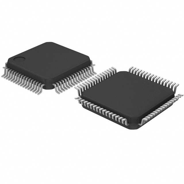


 工商网监
湘ICP备2023018690号
工商网监
湘ICP备2023018690号
