Please note that Cypress is an Infineon Technologies Company.
The document following this cover page is marked as “Cypress” document as this is the
company that originally developed the product. Please note that Infineon will continue
to offer the product to new and existing customers as part of the Infineon product
portfolio.
Continuity of document content
The fact that Infineon offers the following product as part of the Infineon product
portfolio does not lead to any changes to this document. Future revisions will occur
when appropriate, and any changes will be set out on the document history page.
Continuity of ordering part numbers
Infineon continues to support existing part numbers. Please continue to use the
ordering part numbers listed in the datasheet for ordering.
www.infineon.com
�CY91570 Series
32-bit Microcontroller
This series is Cypress 32-bit microcontroller designed for automotive and industrial control applications. It contains the FR81S
CPU that is compatible with the FR family. The FR81S has a high level performance among the Cypress FR family by enhancing
CPU instruction pipeline and load store processing, and improving internal bus transfer.
It is best suited for application control for automotive.
Features
FR81S CPU Core
Peripheral Functions
32-bit RISC, load/store architecture, 5-stage pipeline
Clock generation (equipped with SSCG function)
Maximum operating frequency: 80 MHz (Source oscillation
= 4.0 MHz and 20 multiplied (PLL clock multiplication
system))
16-bit fixed length instructions (basic instruction),
1 instruction per cycle
Instructions appropriate to embedded applications
Memory-to-memory
transfer instruction
processing instruction
Barrel shift instruction etc.
CY91F575:
512 + 64 KB
1024 + 64 KB
CY91F578: 1536 + 64 KB
CY91F579: 2048 + 64 KB
CY91F577:
Built-in Data flash memory (WorkFlash) capacity 64 KB
Bit
Built-in RAM capacity
Main
High-level language support instructions
Register
oscillation (4 MHz)
oscillation (32 kHz) or no sub oscillation
PLL multiplication rate: 1 to 20 times
Sub
Built-in Program flash memory capacity
General-purpose register: 32-bit ×16 sets
Function
Main
CY91F575: 40 KB
entry/exit instructions
content multi-load and store instructions
CY91F577: 64 KB
CY91F578: 96 KB
Bit search instructions
1 detection, 0 detection, and change-point
detection
CY91F579: 128 KB
RAM
CY91F575/7: 8 KB
CY91F578/9: 16 KB
Logical
Backup
Branch instructions with delay slot
Decrease
overhead during branch process
General-purpose ports
Register interlock function
Easy
[LQFP-144]
assembler writing
111
(none sub oscillation), 109 (with sub oscillation)
pseudo open drain ports: 4
P057: Input only
Built-in multiplier and instruction level support
Signed
Signed
Included I2C
32-bit multiplication: 5 cycles
16-bit multiplication: 3 cycles
Interrupt (PC/PS saving)
6
[LQFP-208]
cycles (16 priority levels)
159
The Harvard architecture allows simultaneous execution of
program and data access.
(none sub oscillation), 157 (with sub oscillation)
pseudo open drain ports: 4
P057: Input only
Included I2C
External bus interface
Instruction compatibility with the FR family
22-bit
Built-in memory protection function (MPU)
address, 16-bit data
pins of 9-bit address, 8-bit data, ASX, CS0X, CS1X,
RDX, WR0X, and WR1X can select 5V/3.3V by the VCCE
power supply
23
Eight
protection areas can be specified commonly for
instructions and the data.
Control access privilege in both privilege mode and user
mode.
Built-in FPU (floating point arithmetic)
IEEE754
RAM
DMA Controller
Up
2
to 16 channels can be started simultaneously.
transfer factors (Internal peripheral request and software)
compliant
register 32-bit × 16 sets
Floating-point
Cypress Semiconductor Corporation
Document Number: 002-04725 Rev. *B
•
198 Champion Court
•
San Jose , CA 95134-1709
•
408-943-2600
Revised April 24, 2019
�CY91570 Series
A/D converter (successive approximation type)
8/10-bit
resolution: 40 channels
Conversion time: 3 μs
D/A converter (R-2R type)
8-bit
resolution: 2 channels
External interrupt input: 16 channels
Level
("H" / "L"), or edge detection (rising or falling)
enabled
LIN-UART
6
channels, ch.2 to ch.7
from UART, synchronous mode or LIN-UART
mode
LIN protocol Revision 2.1 supported (LIN-UART).
SPI (Serial Peripheral Interface) supported (synchronous
mode)
Full-duplex double buffering system
LIN synch break detection (linked to the input capture)
Built-in dedicated baud rate generator
DMA transfer support
Selectable
Multi-function serial communication (built-in
transmission/reception FIFO memory): 4 channels
< I2C >
Full-duplex
double buffering system, 16-byte transmission
FIFO memory, 16-byte reception FIFO memory
Standard mode (Max. 100kbps) / high-speed mode (Max.
400kbps) supported
DMA transfer supported (for transmission only)
I2C supporting I/O (for ch.0 and ch.1 only)
CAN Controller (C-CAN): 3 channels
Transfer
speed: Up to 1 Mbps
message buffering: 1 channel,
32-transmission/reception message buffering: 2 channels
64-transmission/reception
PPG: 16-bit × 24 channels
Reload timer: 16-bit × 7 channels (3 channels are for regular
timer interrupt generation.)
Free-run timer:
32-bit × 6 channels (Can select each channel for input
capture, output compare)
Input capture:
32-bit × 12 channels (linked to the free-run timer)
Output compare: 32-bit × 12 channels (linked to the free-run
timer)
< UART (Asynchronous serial interface) >
Full-duplex
double buffering system, 16-byte transmission
FIFO memory, 16-byte reception FIFO memory
Parity or no parity is selectable.
Built-in dedicated baud rate generator
The external clock can be used as the transfer clock
Parity, frame, and overrun error detect functions provided
DMA transfer support
Full-duplex
double buffering system, 16-byte transmission
FIFO, memory, 16-byte reception FIFO memory
SPI supported; master and slave systems supported; 5 to
9-bit data length can be set.
Built-in dedicated baud rate generator (Master operation)
The external clock can be entered. (Slave operation)
Overrun error detection function is provided
DMA transfer support
Full-duplex
double buffering system, 16-byte transmission
FIFO memory, 16-byte reception FIFO memory
LIN protocol revision 2.1 supported
Master and slave systems supported
Framing error and overrun error detection
LIN synch break generation and detection; LIN synch
delimiter generation
Built-in dedicated baud rate generator
The external clock can be adjusted by the reload counter
DMA transfer support
Document Number: 002-04725 Rev. *B
Sound generator: 5 channels
Frequency
and amplitude sequencers provided
Stepping motor controller: 6 channels
8/10-bit
PWM
current output supported (4 lines × 6 channels)
Can refer back electromotive force using pin-shared A/D
converter
High
LCD controller
Common
output: 4, Segment output: 32
drive (SEG0 to SEG31) and static drive (ST0 to ST8)
can be switched.
Each of COM0 to COM3, SEG0 to SEG31, V0, V1, V2, and
V3 pins for duty drive can be switched to the
general-purpose port. (The SEG23 to SEG31 pins can be
switched to static driving.)
V0, V1, V2 and V3 pin can be used as the general-purpose
port. But V3 pin cannot be used as an output pin.
Each of ST0 to ST8 pins for static drive can be switched to
the general-purpose port, or it can be switched to the
segment output of duty drive.
CY91F575/7: The amplitude of the SEG0 to SEG22 output
is determined by the VCC5 power supply pin or by the V3
pin even if VCCE pin is supplied to 3.3 V.
CY91F578/9: The voltage VCCE or less can be supplied to
V3 pin. It is prohibited that VCC5 being chosen as LCDC
reference voltage by software.
Duty
Up/Down counter: 2 channels
8/16-bit
up/down counter
Real-time clock (RTC) (for day, hours, minutes, seconds)
Main
oscillation / sub oscillation frequency can be selected
for the operation clock
Page 2 of 161
�CY91570 Series
Calibration: A hardware watchdog of the CR oscillation drive
and real-time clock (RTC) of the sub clock drive
The CR oscillation frequency can be trimmed
The main clock to sub clock ratio can be corrected by
setting the real-time clock prescaler
Clock Supervisor
Monitoring
abnormality (damage of crystal etc.) of sub
oscillation (32 kHz) (dual clock products) and main
oscillation (4 MHz)
When abnormality is detected, it switches to the CR clock.
Base timer: 2 channels
16-bit
timer
Any of four PWM/PPG/PWC/reload timer functions can be
selected and used.
As for the functions of PWC and reload timer, 2 channels of
cascade mode can be used as 32-bit timer.
CRC generation
HS-SPI
Note: In this series, the HS-SPI function is prohibited
E2PROM and the flash device of the Single/Dual/Quad-SPI
protocol can be connected.
The power supply of 5V/3.3V supplied to the VCCE power
supply pin is used.
Maximum 16 MHz (Maximum 8 MHz at the slave.)
Watchdog timer
Hardware
Software
watchdog
watchdog
Interrupt request batch read
Multiple
interrupts from peripherals can be read by a series
of registers.
I/O relocation
Peripheral
function pins can be reassigned.
Low-power consumption mode
Sleep
Stop
/ Stop / Watch / Sub RUN mode
(power shutdown) / Watch (power shutdown) mode
Power on reset
Low-voltage detection reset (external low-voltage detection)
Low-voltage detection reset (internal low-voltage detection)
Device Package:
LQFP-144
LQFP-208
for CY91F575/7/8/9
for CY91F578/9
CMOS 90nm Technology
Power supplies
5V
Power supply
internal 1.2 V is generated from 5 V with the voltage
step-down regulator.
I/O port uses the power supply of 5V/3.3V supplied to the
VCCE power supply pin.
• LQFP-144: P010 to P017, P020 to P027, and P030 to
P036
• LQFP-208: P140 to P147, P150 to P157, P160 to P167,
P170 to P177, P180 to P187, and P190 to P197
The
NMI
Interrupt controller
Document Number: 002-04725 Rev. *B
Page 3 of 161
�CY91570 Series
Contents
1. Product Lineup .................................................................................................................................................................. 5
2. Pin Assignment (LQFP-144) ........................................................................................................................................... 11
3. Pin Assignment (LQFP-208) ........................................................................................................................................... 12
4. Pin Description (LQFP-144) ............................................................................................................................................ 13
5. Pin Description (LQFP-208) ............................................................................................................................................ 29
6. I/O Circuit Type................................................................................................................................................................ 43
7. Handling Precautions ..................................................................................................................................................... 49
7.1
Precautions for Product Design ................................................................................................................................... 49
7.2
Precautions for Package Mounting .............................................................................................................................. 50
7.3
Precautions for Use Environment ................................................................................................................................ 51
8. Handling Devices ............................................................................................................................................................ 52
9. Block Diagram ................................................................................................................................................................. 55
10. Memory Map .................................................................................................................................................................... 56
11. I/O Map ............................................................................................................................................................................. 60
12. Interrupt Vector Table ................................................................................................................................................... 101
13. Electrical Characteristics ............................................................................................................................................. 104
13.1 Absolute Maximum Ratings ....................................................................................................................................... 104
13.2 Recommended Operating Conditions........................................................................................................................ 106
13.3 DC Characteristics..................................................................................................................................................... 107
13.4 AC Characteristics ..................................................................................................................................................... 114
13.5 A/D Converter ............................................................................................................................................................ 150
13.6 D/A Converter ............................................................................................................................................................ 153
13.7 Flash Memory ............................................................................................................................................................ 154
14. Ordering Information .................................................................................................................................................... 155
15. Package Dimensions .................................................................................................................................................... 156
16. Major Changes .............................................................................................................................................................. 159
Document History ............................................................................................................................................................... 160
Sales, Solutions, and Legal Information ........................................................................................................................... 161
Document Number: 002-04725 Rev. *B
Page 4 of 161
�CY91570 Series
1. Product Lineup
Product
CY91F575B(S)/C(S)
Item
CY91F575BH(S)/CH(S)
System Clock
On chip PLL Clock multiple method
Minimum instruction execution time
Around 12.5 ns (80 MHz)
Sub clock
Yes (Non-S series)
No (S series)
FLASH Capacity (Program)
512 + 64 KB
FLASH Capacity (Work)
64 KB
RAM
40 KB + 8 KB
BI-ROM
4 KB
GDC
None
External BUS I/F
Address: 22-bit Data:16-bit
(Part of the External BUS I/F pins can select the power supply 5 V or 3.3 V)
DMA Controller
16 channels
Base Timer(16-bit)
2 channels
Free-run Timer(32-bit)
6 channels
Input capture(32-bit)
12 channels
Output Compare(32-bit)
12 channels
Reload Timer(16-bit)
7 channels
PPG timer(16-bit)
24 channels
Up/down Counter
2 channels
Clock Supervisor
Yes
D/A converter
2 channels
External Interrupt
16 channels
A/D converter (8-bit/10-bit)
40 channels
LIN-UART
6 channels
Multi-Function serial communication
4 channels*1
HS-SPI
Yes
Up to 16 MHz
Note: In this series, the HS-SPI function is prohibited.
LCD Controller
32 seg × 4 com (Static drive 8seg × 1com)
CAN
64 msg × 1 channel / 32 msg × 2 channels
Stepping Motor Controller
6 channels
Document Number: 002-04725 Rev. *B
Page 5 of 161
�CY91570 Series
Product
CY91F575B(S)/C(S)
Item
Sound Generator
5 channels
Software Watchdog
Yes
Hardware Watchdog
Yes
Clock supervisor
Initial value "ON"
CRC generation
Yes
Low-voltage detection reset
(External low-voltage detection)
Yes
Low-voltage detection reset
(Internal low-voltage detection)
Yes
Package
LQFP-144
Others
Flash Products
On Chip Debug
Yes
CY91F575BH(S)/CH(S)
Initial value "OFF"
*1: I2C only supported by ch.0 and ch.1.
Document Number: 002-04725 Rev. *B
Page 6 of 161
�CY91570 Series
Product
CY91F577B(S)/C(S)
Item
CY91F577BH(S)/CH(S)
System Clock
On chip PLL Clock multiple method
Minimum instruction execution time
Around 12.5 ns (80 MHz)
Sub clock
Yes (Non-S series)
No (S series)
FLASH Capacity (Program)
1024 + 64 KB
FLASH Capacity (Work)
64 KB
RAM
64 KB + 8 KB
BI-ROM
4 KB
GDC
None
External BUS I/F
Address: 22-bit Data:16-bit
(Part of the External BUS I/F pins can select the power supply 5 V or 3.3 V)
DMA Controller
16 channels
Base Timer(16-bit)
2 channels
Free-run Timer(32-bit)
6 channels
Input capture(32-bit)
12 channels
Output Compare(32-bit)
12 channels
Reload Timer(16-bit)
7 channels
PPG timer(16-bit)
24 channels
Up/down Counter
2 channels
Clock Supervisor
Yes
D/A converter
2 channels
External Interrupt
16 channels
A/D converter (8-bit/10-bit)
40 channels
LIN-UART
6 channels
Multi-Function serial communication
4 channels*1
HS-SPI
Yes
Up to 16 MHz
Note: In this series, the HS-SPI function is prohibited.
LCD Controller
32 seg × 4 com (Static drive 8 seg × 1com)
CAN
64 msg × 1 channel / 32 msg × 2 channels
Stepping Motor Controller
6 channels
Sound Generator
5 channels
Document Number: 002-04725 Rev. *B
Page 7 of 161
�CY91570 Series
Product
CY91F577B(S)/C(S)
Item
Software Watchdog
Yes
Hardware Watchdog
Yes
Clock supervisor
Initial value "ON"
CRC generation
Yes
Low-voltage detection reset
(External low-voltage detection)
Yes
Low-voltage detection reset
(Internal low-voltage detection)
Yes
Package
LQFP-144
Others
Flash Products
On Chip Debug
Yes
CY91F577BH(S)/CH(S)
Initial value "OFF"
*1: I2C only supported by ch.0 and ch.1.
Document Number: 002-04725 Rev. *B
Page 8 of 161
�CY91570 Series
Product
CY91F
578C(S)(M)
Item
CY91F
578CH(S)(M)
CY91F
579C(S)(M)
System Clock
On chip PLL Clock multiple method
Minimum instruction execution time
Around 12.5 ns (80 MHz)
Sub clock
Yes (Non-S series)
No (S series)
FLASH Capacity (Program)
1536 + 64 KB
FLASH Capacity (Work)
64 KB
RAM
96 KB + 16 KB
BI-ROM
4 KB
GDC
None
External BUS I/F
Address: 22-bit Data:16-bit
(Part of the External BUS I/F pins can select the power supply 5 V or 3.3 V)
DMA Controller
16 channels
Base Timer(16-bit)
2 channels
Free-run Timer(32-bit)
6 channels
Input capture(32-bit)
12 channels
Output Compare(32-bit)
12 channels
Reload Timer(16-bit)
7 channels
PPG timer(16-bit)
24 channels
Up/down Counter
2 channels
Clock Supervisor
Yes
D/A converter
2 channels
External Interrupt
16 channels
A/D converter (8-bit/10-bit)
40 channels
LIN-UART
6 channels
Multi-Function serial communication
4 channels*1
HS-SPI
No
LCD Controller
32 seg × 4 com (Static drive 8 seg × 1 com)
CAN
64 msg × 1 channel / 32 msg × 2 channels
Stepping Motor Controller
6 channels
Sound Generator
5 channels
Software Watchdog
Yes
Document Number: 002-04725 Rev. *B
CY91F
579CH(S)(M)
2048 + 64 KB
128 KB + 16 KB
Page 9 of 161
�CY91570 Series
Product
CY91F
578C(S)(M)
Item
CY91F
578CH(S)(M)
Hardware Watchdog
Yes
Clock supervisor
Initial value "ON"
CRC generation
Yes
Low-voltage detection reset
(External low-voltage detection)
Yes
Low-voltage detection reset
(Internal low-voltage detection)
Yes
Package
LQFP-144
LQFP-208 (with suffix "M")
Others
Flash Products
On Chip Debug
Yes
Initial value "OFF"
CY91F
579C(S)(M)
Initial value "ON"
CY91F
579CH(S)(M)
Initial value "OFF"
*1: I2C only supported by ch.0 and ch.1.
Document Number: 002-04725 Rev. *B
Page 10 of 161
�CY91570 Series
144
143
142
141
140
139
138
137
136
135
134
133
132
131
130
129
128
127
126
125
124
123
122
121
120
119
118
117
116
115
114
113
112
111
110
109
VSS
P014/D28_0/SEG4/D20_1/INT12_1
P013/D27_0/SEG3/D19_1/INT11_1
P012/D26_0/SEG2/D18_1/INT10_1
P011/D25_0/SEG1/D17_1/INT9_1
P010/D24_0/SEG0/D16_1/INT8_1
P007/D23_0/TOT3_2/PPG7_0/D31_1/INT7_1
P006/D22_0/TOT2_2/PPG6_0/D30_1/INT6_1
P005/D21_0/SCK3_1/TOT1_2/PPG5_0/D29_1/INT5_1
P004/D20_0/SOT3_1/TOT0_2/PPG4_0/D28_1/INT4_1
P003/D19_0/SIN3_1/TIN3_2/PPG3_0/D27_1/INT3_1
P002/D18_0/SCK2_1/TIN2_2/PPG2_0/D26_1/INT2_1
P001/D17_0/SOT2_1/TIN1_2/PPG1_0/D25_1/INT1_1
P000/D16_0/SIN2_1/TIN0_2/PPG0_0/D24_1/INT0_1
C
VSS
VCC5
P134/TRG2/INT5_0/ICU5_0/PPG1_3
P133/SCK1_0/INT3_0/ICU4_0/TIOB1/PPG11_1/TRG5
P132/SOT1_0/INT2_0/ICU3_0/TIOB0
P131/TRG1/SIN1_0/INT4_0/ICU2_0/TIOA1
P130/SCK0_0/INT0_0/ICU1_0/TIOA0
P127/SOT0_0/OCU5_0
P126/TRG0/SIN0_0/INT1_0/OCU4_0
P125/OCU3_0/ICU0_0/PPG10_2
VSS
X1
X0
MD2
MD1
MD0
P124/OCU2_0/ICU5_2/PPG9_2
P096/RX0/INT9_0
P095/TX0/PPG10_1
DEBUGIF
VSS
2. Pin Assignment (LQFP-144)
1
2
3
4
5
6
7
8
9
10
11
12
13
14
15
16
17
18
19
20
21
22
23
24
25
26
27
28
29
30
31
32
33
34
35
36
TOP VIEW
LQFP-144
108
107
106
105
104
103
102
101
100
99
98
97
96
95
94
93
92
91
90
89
88
87
86
85
84
83
82
81
80
79
78
77
76
75
74
73
VCC5
RSTX
P113/RX2/INT11_0/PPG4_2
P112/TX2/PPG3_2
P111/RX1/INT10_0/PPG2_2
P110/TX1/PPG1_2/FRCK5_0
P091/SGA0/SIN2_0/INT12_0/TOT2_1/ICU2_1/PPG6_1
P092/SGO0/SCK2_0/INT13_0/TOT3_1/ICU0_1/PPG7_1
P093/SGA1/SOT2_0/INT14_0/ICU3_1/PPG8_1
P094/SGO1/SIN3_0/INT15_0/ICU1_1/PPG9_1
P097/WOT/SOT3_0/INT8_0/TIN0_0/ICU4_1/PPG0_1
NMIX
P136/(X1A)
P137/(X0A)
VSS
VCC5
P114/SCK3_0/TIN1_0/ICU5_1/SGA2/TRG3/AN32
P115/SIN4_0/TIN2_0/SGO2/FRCK4_0/AN33
P116/SOT4_0/TIN3_0/SGA3/FRCK3_0/AN34
P117/SCK4_0/TOT0_0/SGO3/TRG4/FRCK2_0/AN35
P120/FRCK1_0/SIN5_0/INT6_0/TOT1_0/PPG5_2/AN36
P121/FRCK0_0/SOT5_0/INT7_0/TOT2_0/PPG6_2/AN37
P122/OCU0_0/SCK5_0/TOT3_0/PPG7_2/AN38
P123/OCU1_0/PPG8_2/DAO0/AN39
AVCC
AVRH
AVSS/AVRL
P107/AN7/PPG5_1/DAO1/ICU11_2/SGO4_1
P106/AN6/PPG4_1/ICU10_2/SGA4_1
P105/SCK5_1/AN5/TOT1_1/PPG3_1/ICU9_2
P104/SOT5_1/AN4/TOT0_1/PPG2_1/ICU8_2
P103/SIN5_1/AN3/TIN3_1/PPG1_1/ICU7_2
P102/SCK4_1/AN2/TIN2_1/PPG10_0/ICU6_2
P101/SOT4_1/AN1/TIN1_1/PPG9_0
P100/SIN4_1/AN0/TIN0_1/PPG8_0
P090/ADTG/PPG0_2
VSS
P055/CS2X/V1/FRCK1_1
P056/CS3X/V2/FRCK2_1
P057/RDY/V3/FRCK3_1
DVCC
DVSS
P060/PWM1P0/AN8
P061/PWM1M0/AN9/SIN1_1
P062/PWM2P0/AN10/ZIN1_1/SOT1_1
P063/PWM2M0/AN11/BIN1_1/SCK1_1
P064/PWM1P1/AN12/AIN1_1/SIN0_1
P065/PWM1M1/AN13/ZIN0_1/SOT0_1
P066/PWM2P1/AN14/BIN0_1/SCK0_1
P067/PWM2M1/AN15/AIN0_1/SIN9_1
DVCC
DVSS
P070/PWM1P2/AN16/SOT9_1
P071/PWM1M2/AN17/SCK9_1
P072/PWM2P2/AN18/ICU11_1/SIN8_1
P073/PWM2M2/AN19/ICU10_1/SOT8_1
P074/PWM1P3/AN20/PPG12_1/ICU9_1/SCK8_1
P075/PWM1M3/AN21/PPG13_1/ICU8_1/SIN7_1
P076/PWM2P3/AN22/PPG14_1/ICU7_1/SOT7_1
P077/PWM2M3/AN23/PPG15_1/ICU6_1/SCK7_1
DVCC
DVSS
P080/PWM1P4/AN24/SIN6_0/PPG16_0/AIN0_2
P081/PWM1M4/AN25/SOT6_0/PPG17_0/BIN0_2
P082/PWM2P4/AN26/SCK6_0/PPG18_0/ZIN0_2
P083/PWM2M4/AN27/ICU0_2/PPG19_0
P084/PWM1P5/AN28/ICU1_2/PPG20_0
P085/PWM1M5/AN29/ICU2_2/PPG21_0
P086/PWM2P5/AN30/ICU3_2/PPG22_0
P087/PWM2M5/AN31/ICU4_2/PPG23_0
DVCC
DVSS
37
38
39
40
41
42
43
44
45
46
47
48
49
50
51
52
53
54
55
56
57
58
59
60
61
62
63
64
65
66
67
68
69
70
71
72
VCCE
P015/D29_0/SEG5/D21_1/INT13_1
P016/D30_0/SEG6/D22_1/INT14_1
P017/D31_0/SEG7/D23_1/INT15_1
P020/ASX/SEG8/ICU6_0/OCU0_1
P021/CS0X/SEG9/ICU7_0/OCU1_1
P022/CS1X/SEG10/ICU8_0/OCU2_1
P023/RDX/SEG11/ICU9_0/OCU3_1
P024/WR0X/SEG12/ICU10_0/OCU11_0
P025/WR1X/SEG13/ICU11_0/OCU10_0
P026/A00/SEG14/SPI_CS3/SIN6_1/OCU9_0
P027/A01/SEG15/SPI_CS2/SOT6_1/OCU8_0
P030/A02/SEG16/SPI_CS1/SCK6_1
P031/A03/SEG17/SPI_CS0/SIN9_0
P032/A04/SEG18/SPI_SIO3/SOT9_0/OCU7_0
P033/A05/SEG19/SPI_SIO2/SCK9_0/OCU6_0
P034/A06/SEG20/SPI_SIO1/SIN8_0/OCU5_1
P035/A07/SEG21/SPI_SIO0/SOT8_0/OCU4_1
P036/A08/SEG22/PPG11_0/SPI_CLK/SCK8_0
VCCE
VSS
P037/A09/SEG23/ST0/PPG12_0/SIN7_0
P040/A10/SEG24/ST1/PPG13_0/SOT7_0
P041/A11/SEG25/ST2/PPG14_0/SCK7_0
P042/A12/SEG26/ST3/PPG15_0/AIN0_0
P043/A13/SEG27/ST4/BIN0_0/SGA4_0/OCU6_1
P044/A14/SEG28/ST5/ZIN0_0/SGO4_0/OCU7_1
P045/A15/SEG29/ST6/AIN1_0/SIN8_2
P046/A16/SEG30/ST7/BIN1_0/SOT8_2
P047/A17/SEG31/ST8/ZIN1_0/SCK8_2
P050/A18/COM0/OCU8_1
P051/A19/COM1/OCU9_1
P052/A20/COM2/OCU10_1
P053/A21/COM3/OCU11_1
P054/SYSCLK/V0/FRCK0_1
VCC5
Document Number: 002-04725 Rev. *B
Page 11 of 161
�CY91570 Series
208
207
206
205
204
203
202
201
200
199
198
197
196
195
194
193
192
191
190
189
188
187
186
185
184
183
182
181
180
179
178
177
176
175
174
173
172
171
170
169
168
167
166
165
164
163
162
161
160
159
158
157
VSS
P170/A02
P167/A01
P166/A00
P165/WR1X
P164/WR0X
P163/RDX
P162/CS1X
P161/CS0X
P160/ASX
P157/D31_0/D23_1
P156/D30_0/D22_1
P155/D29_0/D21_1
P154/D28_0/D20_1
P153/D27_0/D19_1
P152/D26_0/D18_1
P151/D25_0/D17_1
P150/D24_0/D16_1
P147/D23_0/D31_1
P146/D22_0/D30_1
P145/D21_0/D29_1
P144/D20_0/D28_1
P143/D19_0/D27_1
P142/D18_0/D26_1
P141/D17_0/D25_1
P140/D16_0/D24_1
C
VSS
VCC5
P134/TRG2/INT5_0/ICU5_0/PPG1_3
P133/SCK1_0/INT3_0/ICU4_0/TIOB1/TRG5/PPG11_1
P132/SOT1_0/INT2_0/ICU3_0/TIOB0
P131/TRG1/SIN1_0/INT4_0/ICU2_0/TIOA1
P130/SCK0_0/INT0_0/ICU1_0/TIOA0
P127/SOT0_0/OCU5_0
P126/TRG0/SIN0_0/INT1_0/OCU4_0
P125/OCU3_0/ICU0_0/PPG10_2
VSS
X1
X0
MD2
MD1
MD0
Non connection
Non connection
Non connection
Non connection
P124/OCU2_0/ICU5_2/PPG9_2
P096/RX0/INT9_0
P095/TX0/PPG10_1
DEBUGIF
VSS
3. Pin Assignment (LQFP-208)
1
2
3
4
5
6
7
8
9
10
11
12
13
14
15
16
17
18
19
20
21
22
23
24
25
26
27
28
29
30
31
32
33
34
35
36
37
38
39
40
41
42
43
44
45
46
47
48
49
50
51
52
○
TOP VIEW
LQFP-208
156
155
154
153
152
151
150
149
148
147
146
145
144
143
142
141
140
139
138
137
136
135
134
133
132
131
130
129
128
127
126
125
124
123
122
121
120
119
118
117
116
115
114
113
112
111
110
109
108
107
106
105
VCC5
RSTX
P113/RX2/INT11_0/PPG4_2
P112/TX2/PPG3_2
P111/RX1/INT10_0/PPG2_2
P110/TX1/PPG1_2/FRCK5_0
P091/SGA0/SIN2_0/INT12_0/TOT2_1/ICU2_1/PPG6_1
P092/SGO0/SCK2_0/INT13_0/TOT3_1/ICU0_1/PPG7_1
P093/SGA1/SOT2_0/INT14_0/ICU3_1/PPG8_1
P094/SGO1/SIN3_0/INT15_0/ICU1_1/PPG9_1
P097/WOT/SOT3_0/INT8_0/TIN0_0/ICU4_1/PPG0_1
Non connection
P007/TOT3_2/PPG7_0/INT7_1
P006/TOT2_2/PPG6_0/INT6_1
P005/SCK3_1/TOT1_2/PPG5_0/INT5_1
P004/SOT3_1/TOT0_2/PPG4_0/INT4_1
NMIX
P136/(X1A)
P137/(X0A)
VSS
VCC5
P003/SIN3_1/TIN3_2/PPG3_0/INT3_1
P002/SCK2_1/TIN2_2/PPG2_0/INT2_1
P001/SOT2_1/TIN1_2/PPG1_0/INT1_1
P000/SIN2_1/TIN0_2/PPG0_0/INT0_1
P114/SCK3_0/TIN1_0/ICU5_1/SGA2/AN32/TRG3
P115/SIN4_0/TIN2_0/SGO2/FRCK4_0/AN33
P116/SOT4_0/TIN3_0/SGA3/FRCK3_0/AN34
P117/SCK4_0/TOT0_0/SGO3/FRCK2_0/AN35/TRG4
P120/FRCK1_0/SIN5_0/INT6_0/TOT1_0/PPG5_2/AN36
P121/FRCK0_0/SOT5_0/INT7_0/TOT2_0/PPG6_2/AN37
P122/OCU0_0/SCK5_0/TOT3_0/PPG7_2/AN38
P123/OCU1_0/PPG8_2/DAO0/AN39
Non connection
AVCC
AVRH
AVSS/AVRL
Non connection
P107/AN7/PPG5_1/DAO1/ICU11_2/SGO4_1
P106/AN6/PPG4_1/ICU10_2/SGA4_1
Non connection
P105/SCK5_1/AN5/TOT1_1/PPG3_1/ICU9_2
P104/SOT5_1/AN4/TOT0_1/PPG2_1/ICU8_2
Non connection
P103/SIN5_1/AN3/TIN3_1/PPG1_1/ICU7_2
P102/SCK4_1/AN2/TIN2_1/PPG10_0/ICU6_2
Non connection
P101/SOT4_1/AN1/TIN1_1/PPG9_0
Non connection
P100/SIN4_1/AN0/TIN0_1/PPG8_0
P090/ADTG/PPG0_2
Non connection
VSS
P037/SEG23/ST0/PPG12_0/SIN7_0
P040/SEG24/ST1/PPG13_0/SOT7_0
P041/SEG25/ST2/PPG14_0/SCK7_0
VCC5
VSS
P042/SEG26/ST3/PPG15_0/AIN0_0
P043/SEG27/ST4/BIN0_0/SGA4_0/OCU6_1
P044/SEG28/ST5/ZIN0_0/SGO4_0/OCU7_1
P045/SEG29/ST6/AIN1_0/SIN8_2
P046/SEG30/ST7/BIN1_0/SOT8_2
P047/SEG31/ST8/ZIN1_0/SCK8_2
P050/COM0/OCU8_1
P051/COM1/OCU9_1
P052/COM2/OCU10_1
P053/COM3/OCU11_1
P054/V0/FRCK0_1
P055/V1/FRCK1_1
P056/V2/FRCK2_1
P057/V3/FRCK3_1
DVCC
DVSS
P060/PWM1P0/AN8
P061/PWM1M0/AN9/SIN1_1
P062/PWM2P0/AN10/SOT1_1/ZIN1_1
P063/PWM2M0/AN11/SCK1_1/BIN1_1
P064/PWM1P1/AN12/SIN0_1/AIN1_1
P065/PWM1M1/AN13/SOT0_1/ZIN0_1
P066/PWM2P1/AN14/SCK0_1/BIN0_1
P067/PWM2M1/AN15/SIN9_1/AIN0_1
DVCC
DVSS
P070/PWM1P2/AN16/SOT9_1
P071/PWM1M2/AN17/SCK9_1
P072/PWM2P2/AN18/SIN8_1/ICU11_1
P073/PWM2M2/AN19/SOT8_1/ICU10_1
P074/PWM1P3/AN20/SCK8_1/ICU9_1/PPG12_1
P075/PWM1M3/AN21/SIN7_1/ICU8_1/PPG13_1
P076/PWM2P3/AN22/SOT7_1/ICU7_1/PPG14_1
P077/PWM2M3/AN23/SCK7_1/ICU6_1/PPG15_1
DVCC
DVSS
P080/PWM1P4/AN24/SIN6_0/PPG16_0/AIN0_2
P081/PWM1M4/AN25/SOT6_0/PPG17_0/BIN0_2
P082/PWM2P4/AN26/SCK6_0/PPG18_0/ZIN0_2
P083/PWM2M4/AN27/ICU0_2/PPG19_0
P084/PWM1P5/AN28/ICU1_2/PPG20_0
P085/PWM1M5/AN29/ICU2_2/PPG21_0
P086/PWM2P5/AN30/ICU3_2/PPG22_0
P087/PWM2M5/AN31/ICU4_2/PPG23_0
DVCC
DVSS
53
54
55
56
57
58
59
60
61
62
63
64
65
66
67
68
69
70
71
72
73
74
75
76
77
78
79
80
81
82
83
84
85
86
87
88
89
90
91
92
93
94
95
96
97
98
99
100
101
102
103
104
VCCE
P171/A03
P172/A04
P173/A05
P174/A06
P175/A07
P176/A08
P177/A09
P180/A10
P181/A11
P182/A12
P183/A13
P184/A14
P185/A15
P186/A16
P187/A17
P190/A18
P191/A19
P192/A20
P193/A21
VCCE
VSS
P194/SYSCLK
P195/CS2X
P196/CS3X
P197/RDY
VCC5
VSS
P010/SEG0/INT8_1
P011/SEG1/INT9_1
P012/SEG2/INT10_1
P013/SEG3/INT11_1
P014/SEG4/INT12_1
P015/SEG5/INT13_1
P016/SEG6/INT14_1
P017/SEG7/INT15_1
P020/SEG8/ICU6_0/OCU0_1
P021/SEG9/ICU7_0/OCU1_1
P022/SEG10/ICU8_0/OCU2_1
P023/SEG11/ICU9_0/OCU3_1
P024/SEG12/ICU10_0/OCU11_0
P025/SEG13/ICU11_0/OCU10_0
P026/SEG14/SIN6_1/OCU9_0
P027/SEG15/SOT6_1/OCU8_0
P030/SEG16/SCK6_1
P031/SEG17/SIN9_0
P032/SEG18/SOT9_0/OCU7_0
P033/SEG19/SCK9_0/OCU6_0
P034/SEG20/SIN8_0/OCU5_1
P035/SEG21/SOT8_0/OCU4_1
P036/SEG22/PPG11_0/SCK8_0
VCC5
Document Number: 002-04725 Rev. *B
Page 12 of 161
�CY91570 Series
4. Pin Description (LQFP-144)
Pin
Number
Pin Name
I/O Circuit
Type
P015
General-Purpose I/O Port
D29_0
2
SEG5
External Bus Data I/O pin
*1
H/I4
External Bus Data I/O pin
INT13_1
External Interrupt Request Input pin ch.13 relocation 1
P016
General-Purpose I/O Port
SEG6
External Bus Data I/O pin
H/I4*1
External Bus Data I/O pin
INT14_1
External Interrupt Request Input pin ch.14 relocation 1
P017
General-Purpose I/O Port
SEG7
External Bus Data I/O pin
*1
H/I4
External Bus Data I/O pin
INT15_1
External Interrupt Request Input pin ch.15 relocation 1
P020
General-Purpose I/O Port
SEG8
External Bus Address-Strobe Output pin
H/I4*1
Input Capture Input pin ch.6 relocation 0
OCU0_1
Output Compare Output pin ch.0 relocation 1
P021
General-Purpose I/O Port
SEG9
External Bus Chip-Select 0 Output pin
*1
H/I4
Input Capture Input pin ch.7 relocation 0
OCU1_1
Output Compare Output pin ch.1 relocation 1
P022
General-Purpose I/O Port
SEG10
External Bus Chip-Select 1 Output pin
H/I4*1
Input Capture Input pin ch.8 relocation 0
OCU2_1
Output Compare Output pin ch.2 relocation 1
P023
General-Purpose I/O Port
SEG11
External Bus Read-Strobe Output pin
*1
H/I4
LCDC Segment(Duty)Output pin
ICU9_0
Input Capture Input pin ch.9 relocation 0
OCU3_1
Output Compare Output pin ch.3 relocation 1
P024
General-Purpose I/O Port
WR0X
9
LCDC Segment(Duty)Output pin
ICU8_0
RDX
8
LCDC Segment(Duty)Output pin
ICU7_0
CS1X
7
LCDC Segment(Duty)Output pin
ICU6_0
CS0X
6
LCDC Segment(Duty)Output pin
D23_1
ASX
5
LCDC Segment(Duty)Output pin
D22_1
D31_0
4
LCDC Segment(Duty)Output pin
D21_1
D30_0
3
Function Description
SEG12
External Bus Write-Strobe 0 Output pin
H/I4*1
LCDC Segment(Duty)Output pin
ICU10_0
Input Capture Input pin ch.10 relocation 0
OCU11_0
Output Compare Output pin ch.11 relocation 0
Document Number: 002-04725 Rev. *B
Page 13 of 161
�CY91570 Series
Pin
Number
Pin Name
I/O Circuit
Type
P025
General-Purpose I/O Port
WR1X
10
11
12
SEG13
External Bus Write-Strobe 1 Output pin
H/I4*1
Input Capture Input pin ch.11 relocation 0
OCU10_0
Output Compare Output pin ch.10 relocation 0
P026
General-Purpose I/O Port
A00
External Bus Address Output pin
SEG14
SPI_CS3
H/I4*1
15
16
LCDC Segment(Duty)Output pin
HS_SPI SSEL3 Output pin (Not supported)
SIN6_1
LIN_UART Serial Input pin ch.6 relocation 1
OCU9_0
Output Compare Output pin ch.9 relocation 0
P027
General-Purpose I/O Port
A01
External Bus Address Output pin
SEG15
SPI_CS2
H/I4*1
LCDC Segment(Duty)Output pin
HS_SPI SSEL2 Output pin (Not supported)
SOT6_1
LIN_UART Serial Output pin ch.6 relocation 1
OCU8_0
Output Compare Output pin ch.8 relocation 0
P030
General-Purpose I/O Port
SEG16
External Bus Address Output pin
*1
H/I4
LCDC Segment(Duty)Output pin
SPI_CS1
HS_SPI SSEL1 Output pin (Not supported)
SCK6_1
LIN_UART Serial Clock I/O pin ch.6 relocation 1
P031
General-Purpose I/O Port
A03
14
LCDC Segment(Duty)Output pin
ICU11_0
A02
13
Function Description
SEG17
External Bus Address Output pin
H/I4*1
LCDC Segment(Duty)Output pin
SPI_CS0
HS_SPI SSEL0 I/O pin (Not supported)
SIN9_0
Multi-function Serial Input pin ch.9 relocation 0
P032
General-Purpose I/O Port
A04
External Bus Address Output pin
SEG18
SPI_SIO3
H/I4*1
LCDC Segment(Duty)Output pin
HS_SPI SDATA3 I/O pin (Not supported)
SOT9_0
Multi-function Serial Output pin ch.9 relocation 0
OCU7_0
Output Compare Output pin ch.7 relocation 0
P033
General-Purpose I/O Port
A05
External Bus Address Output pin
SEG19
SPI_SIO2
H/I4*1
LCDC Segment(Duty)Output pin
HS_SPI SDATA2 I/O pin (Not supported)
SCK9_0
Multi-function Serial Clock I/O pin ch.9 relocation 0
OCU6_0
Output Compare Output pin ch.6 relocation 0
Document Number: 002-04725 Rev. *B
Page 14 of 161
�CY91570 Series
Pin
Number
17
18
19
22
23
24
25
I/O Circuit
Type
Pin Name
Function Description
P034
General-Purpose I/O Port
A06
External Bus Address Output pin
SEG20
SPI_SIO1
H/I4*1
LCDC Segment(Duty)Output pin
HS_SPI SDATA1 I/O pin (Not supported)
SIN8_0
Multi-function Serial Input pin ch.8 relocation 0
OCU5_1
Output Compare Output pin ch.5 relocation 1
P035
General-Purpose I/O Port
A07
External Bus Address Output pin
SEG21
SPI_SIO0
H/I4*1
LCDC Segment(Duty)Output pin
HS_SPI SDATA0 I/O pin (Not supported)
SOT8_0
Multi-function Serial Output pin ch.8 relocation 0
OCU4_1
Output Compare Output pin ch.4 relocation 1
P036
General-Purpose I/O Port
A08
External Bus Address Output pin
SEG22
PPG11_0
H/I4*1
LCDC Segment(Duty)Output pin
PPG Output pin ch.11 relocation 0
SPI_CLK
HS_SPI SCLK I/O pin (Not supported)
SCK8_0
Multi-function Serial Clock I/O pin ch.8 relocation 0
P037
General-Purpose I/O Port
A09
External Bus Address Output pin
SEG23
ST0
I
LCDC Segment(Duty)Output pin
LCDC Segment(Static)Output pin
PPG12_0
PPG Output pin ch.12 relocation 0
SIN7_0
LIN_UART Serial Input pin ch.7 relocation 0
P040
General-Purpose I/O Port
A10
External Bus Address Output pin
SEG24
ST1
I
LCDC Segment(Duty)Output pin
LCDC Segment(Static)Output pin
PPG13_0
PPG Output pin ch.13 relocation 0
SOT7_0
LIN_UART Serial Output pin ch.7 relocation 0
P041
General-Purpose I/O Port
A11
External Bus Address Output pin
SEG25
ST2
I
LCDC Segment(Duty)Output pin
LCDC Segment(Static)Output pin
PPG14_0
PPG Output pin ch.14 relocation 0
SCK7_0
LIN_UART Serial Clock I/O pin ch.7 relocation 0
P042
General-Purpose I/O Port
A12
External Bus Address Output pin
SEG26
ST3
I
LCDC Segment(Duty)Output pin
LCDC Segment(Static)Output pin
PPG15_0
PPG Output pin ch.15 relocation 0
AIN0_0
Up/down Counter AIN Input pin ch.0 relocation 0
Document Number: 002-04725 Rev. *B
Page 15 of 161
�CY91570 Series
Pin
Number
26
I/O Circuit
Type
Pin Name
P043
General-Purpose I/O Port
A13
External Bus Address Output pin
SEG27
LCDC Segment(Duty)Output pin
ST4
I
28
29
30
31
32
LCDC Segment(Static)Output pin
BIN0_0
Up/down Counter BIN Input pin ch.0 relocation 0
SGA4_0
Sound Generator SGA Output pin ch.4 relocation 0
OCU6_1
Output Compare Output pin ch.6 relocation 1
P044
General-Purpose I/O Port
A14
External Bus Address Output pin
SEG28
27
Function Description
ST5
LCDC Segment(Duty)Output pin
I
LCDC Segment(Static)Output pin
ZIN0_0
Up/down Counter ZIN Input pin ch.0 relocation 0
SGO4_0
Sound Generator SGO Output pin ch.4 relocation 0
OCU7_1
Output Compare Output pin ch.7 relocation 1
P045
General-Purpose I/O Port
A15
External Bus Address Output pin
SEG29
ST6
I
LCDC Segment(Duty)Output pin
LCDC Segment(Static)Output pin
AIN1_0
Up/down Counter AIN Input pin ch.1 relocation 0
SIN8_2
Multi-function Serial Input pin ch.8 relocation 2
P046
General-Purpose I/O Port
A16
External Bus Address Output pin
SEG30
ST7
I
LCDC Segment(Duty)Output pin
LCDC Segment(Static)Output pin
BIN1_0
Up/down Counter BIN Input pin ch.1 relocation 0
SOT8_2
Multi-function Serial Output pin ch.8 relocation 2
P047
General-Purpose I/O Port
A17
External Bus Address Output pin
SEG31
ST8
I
LCDC Segment(Duty)Output pin
LCDC Segment(Static)Output pin
ZIN1_0
Up/down Counter ZIN Input pin ch.1 relocation 0
SCK8_2
Multi-function Serial Clock I/O pin ch.8 relocation 2
P050
General-Purpose I/O Port
A18
COM0
I
External Bus Address Output pin
LCDC Segment(Duty)Common Output pin
OCU8_1
Output Compare Output pin ch.8 relocation 1
P051
General-Purpose I/O Port
A19
COM1
OCU9_1
Document Number: 002-04725 Rev. *B
I
External Bus Address Output pin
LCDC Segment(Duty)Common Output pin
Output Compare Output pin ch.9 relocation 1
Page 16 of 161
�CY91570 Series
Pin
Number
I/O Circuit
Type
Pin Name
P052
33
34
35
38
39
40
43
44
45
A20
COM2
General-Purpose I/O Port
I
External Bus Address Output pin
LCDC Segment(Duty)Common Output pin
OCU10_1
Output Compare Output pin ch.10 relocation 1
P053
General-Purpose I/O Port
A21
COM3
I
External Bus Address Output pin
LCDC Segment(Duty)Common Output pin
OCU11_1
Output Compare Output pin ch.11 relocation 1
P054
General-Purpose I/O Port
SYSCLK
V0
I2
External Bus Clock Output pin
LCDC Reference Voltage V0 Input pin
FRCK0_1
Free-Run Timer Clock Input pin ch.0 relocation 1
P055
General-Purpose I/O Port
CS2X
V1
I2
External Bus Chip-Select 2 Output pin
LCDC Reference Voltage V1 Input pin
FRCK1_1
Free-Run Timer Clock Input pin ch.1 relocation 1
P056
General-Purpose I/O Port
CS3X
V2
I2
External Bus Chip-Select 3 Output pin
LCDC Reference Voltage V2 Input pin
FRCK2_1
Free-Run Timer Clock Input pin ch.2 relocation 1
P057
General-Purpose I/O Port (Input only. No output.)
RDY
V3
I3
External Bus RDY Input pin
LCDC Reference Voltage V3 Input pin
FRCK3_1
Free-Run Timer Clock Input pin ch.3 relocation 1
P060
General-Purpose I/O Port
PWM1P0
K
SMC Output pin ch.0
AN8
ADC Analog Input pin ch.8
P061
General-Purpose I/O Port
PWM1M0
AN9
K
SMC Output pin ch.0
ADC Analog Input pin ch.9
SIN1_1
Multi-function Serial Input pin ch.1 relocation 1
P062
General-Purpose I/O Port
PWM2P0
SMC Output pin ch.0
AN10
K
ADC Analog Input pin ch.10
ZIN1_1
Up/down Counter ZIN Input pin ch.1 relocation 1
SOT1_1
Multi-function Serial Output pin ch.1 relocation 1
P063
General-Purpose I/O Port
PWM2M0
46
Function Description
AN11
SMC Output pin ch.0
K
ADC Analog Input pin ch.11
BIN1_1
Up/down Counter BIN Input pin ch.1 relocation 1
SCK1_1
Multi-function Serial Clock I/O pin ch.1 relocation 1
Document Number: 002-04725 Rev. *B
Page 17 of 161
�CY91570 Series
Pin
Number
I/O Circuit
Type
Pin Name
P064
General-Purpose I/O Port
PWM1P1
47
48
AN12
SMC Output pin ch.1
K
50
53
54
Up/down Counter AIN Input pin ch.1 relocation 1
SIN0_1
Multi-function Serial Input pin ch.0 relocation 1
P065
General-Purpose I/O Port
PWM1M1
SMC Output pin ch.1
AN13
K
56
ADC Analog Input pin ch.13
ZIN0_1
Up/down Counter ZIN Input pin ch.0 relocation 1
SOT0_1
Multi-function Serial Output pin ch.0 relocation 1
P066
General-Purpose I/O Port
AN14
SMC Output pin ch.1
K
ADC Analog Input pin ch.14
BIN0_1
Up/down Counter BIN Input pin ch.0 relocation 1
SCK0_1
Multi-function Serial Clock I/O pin ch.0 relocation 1
P067
General-Purpose I/O Port
PWM2M1
SMC Output pin ch.1
AN15
K
ADC Analog Input pin ch.15
AIN0_1
Up/down Counter AIN Input pin ch.0 relocation 1
SIN9_1
Multi-function Serial Input pin ch.9 relocation 1
P070
General-Purpose I/O Port
PWM1P2
AN16
K
SMC Output pin ch.2
ADC Analog Input pin ch.16
SOT9_1
Multi-function Serial Output pin ch.9 relocation 1
P071
General-Purpose I/O Port
PWM1M2
AN17
K
SMC Output pin ch.2
ADC Analog Input pin ch.17
SCK9_1
Multi-function Serial Clock I/O pin ch.9 relocation 1
P072
General-Purpose I/O Port
PWM2P2
55
ADC Analog Input pin ch.12
AIN1_1
PWM2P1
49
Function Description
AN18
SMC Output pin ch.2
K
ADC Analog Input pin ch.18
ICU11_1
Input Capture Input pin ch.11 relocation 1
SIN8_1
Multi-function Serial Input pin ch.8 relocation 1
P073
General-Purpose I/O Port
PWM2M2
SMC Output pin ch.2
AN19
K
ADC Analog Input pin ch.19
ICU10_1
Input Capture Input pin ch.10 relocation 1
SOT8_1
Multi-function Serial Output pin ch.8 relocation 1
Document Number: 002-04725 Rev. *B
Page 18 of 161
�CY91570 Series
Pin
Number
57
58
59
60
63
64
65
I/O Circuit
Type
Pin Name
Function Description
P074
General-Purpose I/O Port
PWM1P3
SMC Output pin ch.3
AN20
PPG12_1
K
ADC Analog Input pin ch.20
PPG Output pin ch.12 relocation 1
ICU9_1
Input Capture Input pin ch.9 relocation 1
SCK8_1
Multi-function Serial Clock I/O pin ch.8 relocation 1
P075
General-Purpose I/O Port
PWM1M3
SMC Output pin ch.3
AN21
PPG13_1
K
ADC Analog Input pin ch.21
PPG Output pin ch.13 relocation 1
ICU8_1
Input Capture Input pin ch.8 relocation 1
SIN7_1
LIN_UART Serial Input pin ch.7 relocation 1
P076
General-Purpose I/O Port
PWM2P3
SMC Output pin ch.3
AN22
PPG14_1
K
ADC Analog Input pin ch.22
PPG Output pin ch.14 relocation 1
ICU7_1
Input Capture Input pin ch.7 relocation 1
SOT7_1
LIN_UART Serial Output pin ch.7 relocation 1
P077
General-Purpose I/O Port
PWM2M3
SMC Output pin ch.3
AN23
PPG15_1
K
ADC Analog Input pin ch.23
PPG Output pin ch.15 relocation 1
ICU6_1
Input Capture Input pin ch.6 relocation 1
SCK7_1
LIN_UART Serial Clock I/O pin ch.7 relocation 1
P080
General-Purpose I/O Port
PWM1P4
SMC Output pin ch.4
AN24
SIN6_0
K
ADC Analog Input pin ch.24
LIN_UART Serial Input pin ch.6 relocation 0
PPG16_0
PPG Output pin ch.16 relocation 0
AIN0_2
Up/down Counter AIN Input pin ch.0 relocation 2
P081
General-Purpose I/O Port
PWM1M4
SMC Output pin ch.4
AN25
SOT6_0
K
ADC Analog Input pin ch.25
LIN_UART Serial Output pin ch.6 relocation 0
PPG17_0
PPG Output pin ch.17 relocation 0
BIN0_2
Up/down Counter BIN Input pin ch.0 relocation 2
P082
General-Purpose I/O Port
PWM2P4
SMC Output pin ch.4
AN26
SCK6_0
K
ADC Analog Input pin ch.26
LIN_UART Serial Clock I/O pin ch.6 relocation 0
PPG18_0
PPG Output pin ch.18 relocation 0
ZIN0_2
Up/down Counter ZIN Input pin ch.0 relocation 2
Document Number: 002-04725 Rev. *B
Page 19 of 161
�CY91570 Series
Pin
Number
I/O Circuit
Type
Pin Name
P083
General-Purpose I/O Port
PWM2M4
66
67
AN27
SMC Output pin ch.4
K
69
Input Capture Input pin ch.0 relocation 2
PPG19_0
PPG Output pin ch.19 relocation 0
P084
General-Purpose I/O Port
PWM1P5
SMC Output pin ch.5
AN28
K
Input Capture Input pin ch.1 relocation 2
PPG20_0
PPG Output pin ch.20 relocation 0
P085
General-Purpose I/O Port
AN29
SMC Output pin ch.5
K
74
Input Capture Input pin ch.2 relocation 2
PPG21_0
PPG Output pin ch.21 relocation 0
P086
General-Purpose I/O Port
PWM2P5
SMC Output pin ch.5
AN30
K
ADC Analog Input pin ch.30
ICU3_2
Input Capture Input pin ch.3 relocation 2
PPG22_0
PPG Output pin ch.22 relocation 0
P087
General-Purpose I/O Port
AN31
SMC Output pin ch.5
K
ADC Analog Input pin ch.31
ICU4_2
Input Capture Input pin ch.4 relocation 2
PPG23_0
PPG Output pin ch.23 relocation 0
ADTG
General-Purpose I/O Port
M
ADC External Trigger Input pin
PPG0_2
PPG Output pin ch.0 relocation 2
P100
General-Purpose I/O Port
SIN4_1
LIN_UART Serial Input pin ch.4 relocation 1
AN0
J
ADC Analog Input pin ch.0
TIN0_1
Reload Timer Event Input pin ch.0 relocation 1
PPG8_0
PPG Output pin ch.8 relocation 0
P101
General-Purpose I/O Port
SOT4_1
75
ADC Analog Input pin ch.29
ICU2_2
P090
73
ADC Analog Input pin ch.28
ICU1_2
PWM2M5
70
ADC Analog Input pin ch.27
ICU0_2
PWM1M5
68
Function Description
AN1
LIN_UART Serial Output pin ch.4 relocation 1
J
ADC Analog Input pin ch.1
TIN1_1
Reload Timer Event Input pin ch.1 relocation 1
PPG9_0
PPG Output pin ch.9 relocation 0
Document Number: 002-04725 Rev. *B
Page 20 of 161
�CY91570 Series
Pin
Number
76
77
78
79
I/O Circuit
Type
Pin Name
P102
General-Purpose I/O Port
SCK4_1
LIN_UART Serial Clock I/O pin ch.4 relocation 1
AN2
TIN2_1
J
85
Reload Timer Event Input pin ch.2 relocation 1
PPG Output pin ch.10 relocation 0
ICU6_2
Input Capture Input pin ch.6 relocation 2
P103
General-Purpose I/O Port
SIN5_1
LIN_UART Serial Input pin ch.5 relocation 1
AN3
TIN3_1
J
ADC Analog Input pin ch.3
Reload Timer Event Input pin ch.3 relocation 1
PPG1_1
PPG Output pin ch.1 relocation 1
ICU7_2
Input Capture Input pin ch.7 relocation 2
P104
General-Purpose I/O Port
SOT5_1
LIN_UART Serial Output pin ch.5 relocation 1
AN4
TOT0_1
J
ADC Analog Input pin ch.4
Reload Timer Output pin ch.0 relocation 1
PPG2_1
PPG Output pin ch.2 relocation 1
ICU8_2
Input Capture Input pin ch.8 relocation 2
P105
General-Purpose I/O Port
SCK5_1
LIN_UART Serial Clock I/O pin ch.5 relocation 1
AN5
J
ADC Analog Input pin ch.5
Reload Timer Output pin ch.1 relocation 1
PPG3_1
PPG Output pin ch.3 relocation 1
ICU9_2
Input Capture Input pin ch.9 relocation 2
P106
General-Purpose I/O Port
AN6
81
ADC Analog Input pin ch.2
PPG10_0
TOT1_1
80
Function Description
PPG4_1
ADC Analog Input pin ch.6
J
PPG Output pin ch.4 relocation 1
ICU10_2
Input Capture Input pin ch.10 relocation 2
SGA4_1
Sound Generator SGA Output pin ch.4 relocation 1
P107
General-Purpose I/O Port
AN7
ADC Analog Input pin ch.7
PPG5_1
DAO1
L
PPG Output pin ch.5 relocation 1
DAC Output pin ch.1
ICU11_2
Input Capture Input pin ch.11 relocation 2
SGO4_1
Sound Generator SGO Output pin ch.4 relocation 1
P123
General-Purpose I/O Port
OCU1_0
Output Compare Output pin ch.1 relocation 0
PPG8_2
L
PPG Output pin ch.8 relocation 2
DAO0
DAC Output pin ch.0
AN39
ADC Analog Input pin ch.39
Document Number: 002-04725 Rev. *B
Page 21 of 161
�CY91570 Series
Pin
Number
86
87
I/O Circuit
Type
Pin Name
P122
General-Purpose I/O Port
OCU0_0
Output Compare Output pin ch.0 relocation 0
SCK5_0
TOT3_0
J
90
AN38
ADC Analog Input pin ch.38
P121
General-Purpose I/O Port
FRCK0_0
Free-Run Timer Clock Input pin ch.0 relocation 0
SOT5_0
LIN_UART Serial Output pin ch.5 relocation 0
INT7_0
J
External Interrupt Request Input pin ch.7 relocation 0
TOT2_0
Reload Timer Output pin ch.2 relocation 0
PPG6_2
PPG Output pin ch.6 relocation 2
AN37
ADC Analog Input pin ch.37
P120
General-Purpose I/O Port
FRCK1_0
Free-Run Timer Clock Input pin ch.1 relocation 0
INT6_0
LIN_UART Serial Input pin ch.5 relocation 0
J
External Interrupt Request Input pin ch.6 relocation 0
TOT1_0
Reload Timer Output pin ch.1 relocation 0
PPG5_2
PPG Output pin ch.5 relocation 2
AN36
ADC Analog Input pin ch.36
P117
General-Purpose I/O Port
SCK4_0
LIN_UART Serial Clock I/O pin ch.4 relocation 0
SGO3
Reload Timer Output pin ch.0 relocation 0
J
Sound Generator SGO Output pin ch.3
TRG4
PPG Trigger Input pin 4 (ch.16-ch.19)
FRCK2_0
Free-Run Timer Clock Input pin ch.2 relocation 0
AN35
ADC Analog Input pin ch.35
P116
General-Purpose I/O Port
SOT4_0
LIN_UART Serial Output pin ch.4 relocation 0
TIN3_0
SGA3
91
Reload Timer Output pin ch.3 relocation 0
PPG Output pin ch.7 relocation 2
TOT0_0
89
LIN_UART Serial Clock I/O pin ch.5 relocation 0
PPG7_2
SIN5_0
88
Function Description
J
Reload Timer Event Input pin ch.3 relocation 0
Sound Generator SGA Output pin ch.3
FRCK3_0
Free-Run Timer Clock Input pin ch.3 relocation 0
AN34
ADC Analog Input pin ch.34
P115
General-Purpose I/O Port
SIN4_0
LIN_UART Serial Input pin ch.4 relocation 0
TIN2_0
SGO2
J
Reload Timer Event Input pin ch.2 relocation 0
Sound Generator SGO Output pin ch.2
FRCK4_0
Free-Run Timer Clock Input pin ch.4 relocation 0
AN33
ADC Analog Input pin ch.33
Document Number: 002-04725 Rev. *B
Page 22 of 161
�CY91570 Series
Pin
Number
I/O Circuit
Type
Pin Name
P114
General-Purpose I/O Port
SCK3_0
LIN_UART Serial Clock I/O pin ch.3 relocation 0
TIN1_0
92
95
96
97
98
99
100
ICU5_1
Reload Timer Event Input pin ch.1 relocation 0
J
Input Capture Input pin ch.5 relocation 1
SGA2
Sound Generator SGA Output pin ch.2
TRG3
PPG Trigger Input pin 3 (ch.12-ch.15)
AN32
ADC Analog Input pin ch.32
P137
(X0A)
P136
(X1A)
NMIX
M (Y)
M (Y)
R
General-Purpose I/O Port
Sub Clock oscillation Input pin (only dual clock product)
General-Purpose I/O Port
Sub Clock oscillation Output pin (only dual clock product)
NMI Pin
P097
General-Purpose I/O Port
WOT
RTC Overflow Output pin
SOT3_0
LIN_UART Serial Output pin ch.3 relocation 0
INT8_0
M
External Interrupt Request Input pin ch.8 relocation 0
TIN0_0
Reload Timer Event Input pin ch.0 relocation 0
ICU4_1
Input Capture Input pin ch.4 relocation 1
PPG0_1
PPG Output pin ch.0 relocation 1
P094
General-Purpose I/O Port
SGO1
Sound Generator SGO Output pin ch.1
SIN3_0
INT15_0
M
LIN_UART Serial Input pin ch.3 relocation 0
External Interrupt Request Input pin ch.15 relocation 0
ICU1_1
Input Capture Input pin ch.1 relocation 1
PPG9_1
PPG Output pin ch.9 relocation 1
P093
General-Purpose I/O Port
SGA1
Sound Generator SGA Output pin ch.1
SOT2_0
INT14_0
M
LIN_UART Serial Output pin ch.2 relocation 0
External Interrupt Request Input pin ch.14 relocation 0
ICU3_1
Input Capture Input pin ch.3 relocation 1
PPG8_1
PPG Output pin ch.8 relocation 1
P092
General-Purpose I/O Port
SGO0
Sound Generator SGO Output pin ch.0
SCK2_0
101
Function Description
INT13_0
LIN_UART Serial Clock I/O pin ch.2 relocation 0
M
External Interrupt Request Input pin ch.13 relocation 0
TOT3_1
Reload Timer Output pin ch.3 relocation 1
ICU0_1
Input Capture Input pin ch.0 relocation 1
PPG7_1
PPG Output pin ch.7 relocation 1
Document Number: 002-04725 Rev. *B
Page 23 of 161
�CY91570 Series
Pin
Number
102
103
104
I/O Circuit
Type
Pin Name
P091
General-Purpose I/O Port
SGA0
Sound Generator SGA Output pin ch.0
SIN2_0
LIN_UART Serial Input pin ch.2 relocation 0
INT12_0
M
Reload Timer Output pin ch.2 relocation 1
ICU2_1
Input Capture Input pin ch.2 relocation 1
PPG6_1
PPG Output pin ch.6 relocation 1
P110
General-Purpose I/O Port
TX1
PPG1_2
M
CAN TX Data Output pin ch.1
PPG Output pin ch.1 relocation 2
FRCK5_0
Free-Run Timer Clock Input pin ch.5 relocation 0
P111
General-Purpose I/O Port
RX1
INT10_0
M
TX2
CAN RX Data Input pin ch.1
External Interrupt Request Input pin ch.10 relocation 0
PPG Output pin ch.2 relocation 2
P112
106
External Interrupt Request Input pin ch.12 relocation 0
TOT2_1
PPG2_2
105
Function Description
General-Purpose I/O Port
M
CAN TX Data Output pin ch.2
PPG3_2
PPG Output pin ch.3 relocation 2
P113
General-Purpose I/O Port
RX2
INT11_0
M
PPG4_2
CAN RX Data Input pin ch.2
External Interrupt Request Input pin ch.11 relocation 0
PPG Output pin ch.4 relocation 2
107
RSTX
R
Reset Pin
110
DEBUGIF
B
DEBUG I/F pin
P095
111
TX0
General-Purpose I/O Port
M
PPG10_1
PPG Output pin ch.10 relocation 1
P096
112
113
RX0
CAN TX Data Output pin ch.0
General-Purpose I/O Port
M
CAN RX Data Input pin ch.0
INT9_0
External Interrupt Request Input pin ch.9 relocation 0
P124
General-Purpose I/O Port
OCU2_0
ICU5_2
M
PPG9_2
Output Compare Output pin ch.2 relocation 0
Input Capture Input pin ch.5 relocation 2
PPG Output pin ch.9 relocation 2
114
MD0
A
Mode Pin 0
115
MD1
A
Mode Pin 1
116
MD2
R2
Mode Pin 2
117
X0
X
Main Clock oscillation Input pin
118
X1
X
Main Clock oscillation Output pin
P125
120
OCU3_0
ICU0_0
PPG10_2
Document Number: 002-04725 Rev. *B
General-Purpose I/O Port
M
Output Compare Output pin ch.3 relocation 0
Input Capture Input pin ch.0 relocation 0
PPG Output pin ch.10 relocation 2
Page 24 of 161
�CY91570 Series
Pin
Number
I/O Circuit
Type
Pin Name
P126
General-Purpose I/O Port
TRG0
121
SIN0_0
PPG Trigger Input pin 0 (ch.0-ch.3)
M
External Interrupt Request Input pin ch.1 relocation 0
OCU4_0
Output Compare Output pin ch.4 relocation 0
SOT0_0
General-Purpose I/O Port
N
124
125
126
127
131
Multi-function Serial Output pin ch.0 relocation 0
OCU5_0
Output Compare Output pin ch.5 relocation 0
P130
General-Purpose I/O Port
SCK0_0
123
Multi-function Serial Input pin ch.0 relocation 0
INT1_0
P127
122
Function Description
INT0_0
Multi-function Serial Clock I/O pin ch.0 relocation 0
N
External Interrupt Request Input pin ch.0 relocation 0
ICU1_0
Input Capture Input pin ch.1 relocation 0
TIOA0
Base Timer Output pin ch.0
P131
General-Purpose I/O Port
TRG1
PPG Trigger Input pin 1 (ch.4-ch.7)
SIN1_0
INT4_0
M
Multi-function Serial Input pin ch.1 relocation 0
External Interrupt Request Input pin ch.4 relocation 0
ICU2_0
Input Capture Input pin ch.2 relocation 0
TIOA1
Base Timer I/O pin ch.1
P132
General-Purpose I/O Port
SOT1_0
Multi-function Serial Output pin ch.1 relocation 0
INT2_0
N
External Interrupt Request Input pin ch.2 relocation 0
ICU3_0
Input Capture Input pin ch.3 relocation 0
TIOB0
Base Timer Input pin ch.0
P133
General-Purpose I/O Port
SCK1_0
Multi-function Serial Clock I/O pin ch.1 relocation 0
INT3_0
External Interrupt Request Input pin ch.3 relocation 0
ICU4_0
N
Input Capture Input pin ch.4 relocation 0
TIOB1
Base Timer Input pin ch.1
PPG11_1
PPG Output pin ch.11 relocation 1
TRG5
PPG Trigger Input pin 5 (ch.20-ch.23)
P134
General-Purpose I/O Port
TRG2
PPG Trigger Input pin 2 (ch.8-ch.11)
INT5_0
M
External Interrupt Request Input pin ch.5 relocation 0
ICU5_0
Input Capture Input pin ch.5 relocation 0
PPG1_3
PPG Output pin ch.1 relocation 3
P000
General-Purpose I/O Port
D16_0
External Bus Data I/O pin
SIN2_1
LIN_UART Serial Input pin ch.2 relocation 1
TIN0_2
M
Reload Timer Event Input pin ch.0 relocation 2
PPG0_0
PPG Output pin ch.0 relocation 0
D24_1
External Bus Data I/O pin
INT0_1
External Interrupt Request Input pin ch.0 relocation 1
Document Number: 002-04725 Rev. *B
Page 25 of 161
�CY91570 Series
Pin
Number
132
I/O Circuit
Type
Pin Name
P001
General-Purpose I/O Port
D17_0
External Bus Data I/O pin
SOT2_1
LIN_UART Serial Output pin ch.2 relocation 1
TIN1_2
M
134
PPG Output pin ch.1 relocation 0
D25_1
External Bus Data I/O pin
INT1_1
External Interrupt Request Input pin ch.1 relocation 1
P002
General-Purpose I/O Port
D18_0
External Bus Data I/O pin
TIN2_2
LIN_UART Serial Clock I/O pin ch.2 relocation 1
M
136
137
Reload Timer Event Input pin ch.2 relocation 2
PPG2_0
PPG Output pin ch.2 relocation 0
D26_1
External Bus Data I/O pin
INT2_1
External Interrupt Request Input pin ch.2 relocation 1
P003
General-Purpose I/O Port
D19_0
External Bus Data I/O pin
SIN3_1
LIN_UART Serial Input pin ch.3 relocation 1
TIN3_2
M
Reload Timer Event Input pin ch.3 relocation 2
PPG3_0
PPG Output pin ch.3 relocation 0
D27_1
External Bus Data I/O pin
INT3_1
External Interrupt Request Input pin ch.3 relocation 1
P004
General-Purpose I/O Port
D20_0
External Bus Data I/O pin
SOT3_1
135
Reload Timer Event Input pin ch.1 relocation 2
PPG1_0
SCK2_1
133
Function Description
TOT0_2
LIN_UART Serial Output pin ch.3 relocation 1
M
Reload Timer Output pin ch.0 relocation 2
PPG4_0
PPG Output pin ch.4 relocation 0
D28_1
External Bus Data I/O pin
INT4_1
External Interrupt Request Input pin ch.4 relocation 1
P005
General-Purpose I/O Port
D21_0
External Bus Data I/O pin
SCK3_1
LIN_UART Serial Clock I/O pin ch.3 relocation 1
TOT1_2
M
Reload Timer Output pin ch.1 relocation 2
PPG5_0
PPG Output pin ch.5 relocation 0
D29_1
External Bus Data I/O pin
INT5_1
External Interrupt Request Input pin ch.5 relocation 1
P006
General-Purpose I/O Port
D22_0
External Bus Data I/O pin
TOT2_2
PPG6_0
M
Reload Timer Output pin ch.2 relocation 2
PPG Output pin ch.6 relocation 0
D30_1
External Bus Data I/O pin
INT6_1
External Interrupt Request Input pin ch.6 relocation 1
Document Number: 002-04725 Rev. *B
Page 26 of 161
�CY91570 Series
Pin
Number
138
I/O Circuit
Type
Pin Name
P007
General-Purpose I/O Port
D23_0
External Bus Data I/O pin
TOT3_2
PPG7_0
Reload Timer Output pin ch.3 relocation 2
M
PPG Output pin ch.7 relocation 0
D31_1
External Bus Data I/O pin
INT7_1
External Interrupt Request Input pin ch.7 relocation 1
P010
General-Purpose I/O Port
D24_0
139
SEG0
External Bus Data I/O pin
H/I4*1
External Bus Data I/O pin
INT8_1
External Interrupt Request Input pin ch.8 relocation 1
P011
General-Purpose I/O Port
SEG1
External Bus Data I/O pin
*1
H/I4
External Bus Data I/O pin
INT9_1
External Interrupt Request Input pin ch.9 relocation 1
P012
General-Purpose I/O Port
SEG2
External Bus Data I/O pin
H/I4*1
External Bus Data I/O pin
INT10_1
External Interrupt Request Input pin ch.10 relocation 1
P013
General-Purpose I/O Port
SEG3
External Bus Data I/O pin
*1
H/I4
LCDC Segment(Duty)Output pin
D19_1
External Bus Data I/O pin
INT11_1
External Interrupt Request Input pin ch.11 relocation 1
P014
General-Purpose I/O Port
D28_0
143
LCDC Segment(Duty)Output pin
D18_1
D27_0
142
LCDC Segment(Duty)Output pin
D17_1
D26_0
141
LCDC Segment(Duty)Output pin
D16_1
D25_0
140
Function Description
SEG4
External Bus Data I/O pin
H/I4*1
LCDC Segment(Duty)Output pin
D20_1
External Bus Data I/O pin
INT12_1
External Interrupt Request Input pin ch.12 relocation 1
1
VCCE
-
+3.3v/+5.0v Power Supply pin
20
VCCE
-
+3.3v/+5.0v Power Supply pin
21
VSS
-
GND pin
36
VCC5
-
+5.0v Power Supply pin
37
VSS
-
GND pin
41
DVCC
-
Power Supply pin for SMC high current
42
DVSS
-
GND pin for SMC high current
51
DVCC
-
Power Supply pin for SMC high current
52
DVSS
-
GND pin for SMC high current
61
DVCC
-
Power Supply pin for SMC high current
62
DVSS
-
GND pin for SMC high current
71
DVCC
-
Power Supply pin for SMC high current
Document Number: 002-04725 Rev. *B
Page 27 of 161
�CY91570 Series
Pin
Number
I/O Circuit
Type
Pin Name
Function Description
72
DVSS
-
GND pin for SMC high current
82
AVSS/AVRL
-
ADC, DAC GND pin / Low Reference Voltage pin
83
AVRH
-
ADC High Reference Voltage pin
84
AVCC
-
ADC,DAC Analog Power Supply pin
93
VCC5
-
+5.0v Power Supply pin
94
VSS
-
GND pin
108
VCC5
-
+5.0v Power Supply pin
109
VSS
-
GND pin
119
VSS
-
GND pin
128
VCC5
-
+5.0v Power Supply pin
129
VSS
-
GND pin
130
C
-
External Capacitance Connection Pin
144
VSS
-
GND pin
*1: I/O circuit type H is applied to CY91F575/7 and type I4 applied to CY91F578/9.
Document Number: 002-04725 Rev. *B
Page 28 of 161
�CY91570 Series
5. Pin Description (LQFP-208)
Pin Number
1
2
3
4
5
6
7
8
9
10
11
12
13
14
15
16
17
18
19
20
Pin Name
VCCE
P171
A03
P172
A04
P173
A05
P174
A06
P175
A07
P176
A08
P177
A09
P180
A10
P181
A11
P182
A12
P183
A13
P184
A14
P185
A15
P186
A16
P187
A17
P190
A18
P191
A19
P192
A20
P193
A21
I/O Circuit Type
M2
M2
M2
M2
M2
M2
M2
M2
M2
M2
M2
M2
M2
M2
M2
M2
M2
M2
M2
Function Description
+3.3v/+5.0v Power Supply pin
General-Purpose I/O Port
External Bus Address Output pin
General-Purpose I/O Port
External Bus Address Output pin
General-Purpose I/O Port
External Bus Address Output pin
General-Purpose I/O Port
External Bus Address Output pin
General-Purpose I/O Port
External Bus Address Output pin
General-Purpose I/O Port
External Bus Address Output pin
General-Purpose I/O Port
External Bus Address Output pin
General-Purpose I/O Port
External Bus Address Output pin
General-Purpose I/O Port
External Bus Address Output pin
General-Purpose I/O Port
External Bus Address Output pin
General-Purpose I/O Port
External Bus Address Output pin
General-Purpose I/O Port
External Bus Address Output pin
General-Purpose I/O Port
External Bus Address Output pin
General-Purpose I/O Port
External Bus Address Output pin
General-Purpose I/O Port
External Bus Address Output pin
General-Purpose I/O Port
External Bus Address Output pin
General-Purpose I/O Port
External Bus Address Output pin
General-Purpose I/O Port
External Bus Address Output pin
General-Purpose I/O Port
External Bus Address Output pin
21
VCCE
-
+3.3v/+5.0v Power Supply pin
22
VSS
-
GND pin
23
24
25
26
P194
SYSCLK
P195
CS2X
P196
CS3X
P197
RDY
M2
M2
M2
M2
Document Number: 002-04725 Rev. *B
General-Purpose I/O Port
External Bus Clock Output pin
General-Purpose I/O Port
External Bus Chip-Select 2 Output pin
General-Purpose I/O Port
External Bus Chip-Select 3 Output pin
General-Purpose I/O Port
External Bus RDY Input pin
Page 29 of 161
�CY91570 Series
Pin Number
Pin Name
I/O Circuit Type
Function Description
27
VCC5
-
+5.0v Power Supply pin
28
VSS
-
GND pin
29
29
P010
SEG0
INT8_1
H
H
P011
30
SEG1
General-Purpose I/O Port
I
INT11_1
SEG4
General-Purpose I/O Port
I
INT12_1
35
SEG5
General-Purpose I/O Port
I
External Interrupt Request Input pin ch.13 relocation 1
P016
General-Purpose I/O Port
SEG6
I
38
39
40
41
42
SEG7
LCDC Segment(Duty)Output pin
External Interrupt Request Input pin ch.14 relocation 1
P017
37
LCDC Segment(Duty)Output pin
INT13_1
INT14_1
36
LCDC Segment(Duty)Output pin
External Interrupt Request Input pin ch.12 relocation 1
P015
34
LCDC Segment(Duty)Output pin
External Interrupt Request Input pin ch.11 relocation 1
P014
33
LCDC Segment(Duty)Output pin
External Interrupt Request Input pin ch.10 relocation 1
P013
SEG3
LCDC Segment(Duty)Output pin
General-Purpose I/O Port
I
INT10_1
32
External Interrupt Request Input pin ch.8 relocation 1
External Interrupt Request Input pin ch.9 relocation 1
P012
SEG2
LCDC Segment(Duty)Output pin
General-Purpose I/O Port
I
INT9_1
31
General-Purpose I/O Port
General-Purpose I/O Port
I
LCDC Segment(Duty)Output pin
INT15_1
External Interrupt Request Input pin ch.15 relocation 1
P020
General-Purpose I/O Port
SEG8
ICU6_0
I
LCDC Segment(Duty)Output pin
Input Capture Input pin ch.6 relocation 0
OCU0_1
Output Compare Output pin ch.0 relocation 1
P021
General-Purpose I/O Port
SEG9
ICU7_0
I
LCDC Segment(Duty)Output pin
Input Capture Input pin ch.7 relocation 0
OCU1_1
Output Compare Output pin ch.1 relocation 1
P022
General-Purpose I/O Port
SEG10
ICU8_0
I
LCDC Segment(Duty)Output pin
Input Capture Input pin ch.8 relocation 0
OCU2_1
Output Compare Output pin ch.2 relocation 1
P023
General-Purpose I/O Port
SEG11
ICU9_0
I
LCDC Segment(Duty)Output pin
Input Capture Input pin ch.9 relocation 0
OCU3_1
Output Compare Output pin ch.3 relocation 1
P024
General-Purpose I/O Port
SEG12
ICU10_0
I
LCDC Segment(Duty)Output pin
Input Capture Input pin ch.10 relocation 0
OCU11_0
Output Compare Output pin ch.11 relocation 0
P025
General-Purpose I/O Port
SEG13
ICU11_0
I
OCU10_0
Document Number: 002-04725 Rev. *B
LCDC Segment(Duty)Output pin
Input Capture Input pin ch.11 relocation 0
Output Compare Output pin ch.10 relocation 0
Page 30 of 161
�CY91570 Series
Pin Number
Pin Name
I/O Circuit Type
P026
43
44
45
45
SEG14
SIN6_1
I
47
48
49
50
51
LCDC Segment(Duty)Output pin
LIN_UART Serial Input pin ch.6 relocation 1
OCU9_0
Output Compare Output pin ch.9 relocation 0
P027
General-Purpose I/O Port
SEG15
I
SOT6_1
LCDC Segment(Duty)Output pin
LIN_UART Serial Output pin ch.6 relocation 1
OCU8_0
I
Output Compare Output pin ch.8 relocation 8
P030
I
General-Purpose I/O Port
SEG16
SCK6_1
I
P031
46
Function Description
General-Purpose I/O Port
SEG17
LCDC Segment(Duty)Output pin
LIN_UART Serial Clock I/O pin ch.6 relocation 1
General-Purpose I/O Port
I
LCDC Segment(Duty)Output pin
SIN9_0
Multi-function Serial Input pin ch.9 relocation 0
P032
General-Purpose I/O Port
SEG18
SOT9_0
I
LCDC Segment(Duty)Output pin
Multi-function Serial Output pin ch.9 relocation 0
OCU7_0
Output Compare Output pin ch.7 relocation 7
P033
General-Purpose I/O Port
SEG19
SCK9_0
I
LCDC Segment(Duty)Output pin
Multi-function Serial Clock I/O pin ch.9 relocation 0
OCU6_0
Output Compare Output pin ch.6 relocation 6
P034
General-Purpose I/O Port
SEG20
SIN8_0
I
LCDC Segment(Duty)Output pin
Multi-function Serial Input pin ch.8 relocation 0
OCU5_1
Output Compare Output pin ch.5 relocation 1
P035
General-Purpose I/O Port
SEG21
SOT8_0
I
LCDC Segment(Duty)Output pin
Multi-function Serial Output pin ch.8 relocation 0
OCU4_1
Output Compare Output pin ch.4 relocation 1
P036
General-Purpose I/O Port
SEG22
PPG11_0
I
SCK8_0
LCDC Segment(Duty)Output pin
PPG Output pin ch.11 relocation 0
Multi-function Serial Clock I/O pin ch.8 relocation 0
52
VCC5
-
+5.0v Power Supply pin
53
VSS
-
GND pin
P037
General-Purpose I/O Port
SEG23
54
ST0
LCDC Segment(Duty)Output pin
I
PPG Output pin ch.12 relocation 0
SIN7_0
LIN_UART Serial Input pin ch.7 relocation 0
P040
General-Purpose I/O Port
SEG24
55
LCDC Segment(Static)Output pin
PPG12_0
ST1
LCDC Segment(Duty)Output pin
I
LCDC Segment(Static)Output pin
PPG13_0
PPG Output pin ch.13 relocation 0
SOT7_0
LIN_UART Serial Output pin ch.7 relocation 0
Document Number: 002-04725 Rev. *B
Page 31 of 161
�CY91570 Series
Pin Number
Pin Name
I/O Circuit Type
P041
SEG25
56
ST2
Function Description
General-Purpose I/O Port
LCDC Segment(Duty)Output pin
I
LCDC Segment(Static)Output pin
PPG14_0
PPG Output pin ch.14 relocation 0
SCK7_0
LIN_UART Serial Clock I/O pin ch.7 relocation 0
57
VCC5
-
+5.0v Power Supply pin
58
VSS
-
GND pin
P042
General-Purpose I/O Port
SEG26
59
60
61
ST3
LCDC Segment(Duty)Output pin
I
PPG Output pin ch.15 relocation 0
AIN0_0
Up/down Counter AIN Input pin ch.0 relocation 0
P043
General-Purpose I/O Port
SEG27
LCDC Segment(Duty)Output pin
ST4
BIN0_0
I
Sound Generator SGA Output pin ch.4 relocation 0
Output Compare Output pin ch.6 relocation 1
P044
General-Purpose I/O Port
SEG28
LCDC Segment(Duty)Output pin
ST5
ZIN0_0
I
Sound Generator SGO Output pin ch.4 relocation 0
Output Compare Output pin ch.7 relocation 1
P045
General-Purpose I/O Port
ST6
LCDC Segment(Duty)Output pin
I
Up/down Counter AIN Input pin ch.1 relocation 0
SIN8_2
Multi-function Serial Input pin ch.8 relocation 2
P046
General-Purpose I/O Port
ST7
LCDC Segment(Duty)Output pin
I
LCDC Segment(Static)Output pin
BIN1_0
Up/down Counter BIN Input pin ch.1 relocation 0
SOT8_2
Multi-function Serial Output pin ch.8 relocation 2
P047
General-Purpose I/O Port
ST8
LCDC Segment(Duty)Output pin
I
LCDC Segment(Static)Output pin
ZIN1_0
Up/down Counter ZIN Input pin ch.1 relocation 0
SCK8_2
Multi-function Serial Clock I/O pin ch.8 relocation 2
COM0
General-Purpose I/O Port
I
COM1
General-Purpose I/O Port
I
OCU9_1
LCDC Segment(Duty)Common Output pin
Output Compare Output pin ch.9 relocation 1
P052
COM2
LCDC Segment(Duty)Common Output pin
Output Compare Output pin ch.8 relocation 1
P051
67
LCDC Segment(Static)Output pin
AIN1_0
OCU8_1
66
Up/down Counter ZIN Input pin ch.0 relocation 0
OCU7_1
P050
65
LCDC Segment(Static)Output pin
SGO4_0
SEG31
64
Up/down Counter BIN Input pin ch.0 relocation 0
OCU6_1
SEG30
63
LCDC Segment(Static)Output pin
SGA4_0
SEG29
62
LCDC Segment(Static)Output pin
PPG15_0
General-Purpose I/O Port
I
OCU10_1
Document Number: 002-04725 Rev. *B
LCDC Segment(Duty)Common Output pin
Output Compare Output pin ch.10 relocation 1
Page 32 of 161
�CY91570 Series
Pin Number
Pin Name
I/O Circuit Type
P053
68
COM3
I
OCU11_1
V0
General-Purpose I/O Port
I2
FRCK0_1
V1
General-Purpose I/O Port
I2
FRCK1_1
72
V2
LCDC Reference Voltage V1 Input pin
Free-Run Timer Clock Input pin ch.1 relocation 1
P056
71
LCDC Reference Voltage V0 Input pin
Free-Run Timer Clock Input pin ch.0 relocation 1
P055
70
LCDC Segment(Duty)Common Output pin
Output Compare Output pin ch.11 relocation 1
P054
69
Function Description
General-Purpose I/O Port
General-Purpose I/O Port
I2
LCDC Reference Voltage V2 Input pin
FRCK2_1
Free-Run Timer Clock Input pin ch.2 relocation 1
P057
General-Purpose I/O Port
V3
I3
FRCK3_1
LCDC Reference Voltage V3 Input pin
Free-Run Timer Clock Input pin ch.3 relocation 1
73
DVCC
-
Power Supply pin for SMC high current
74
DVSS
-
GND pin for SMC high current
P060
75
76
PWM1P0
General-Purpose I/O Port
K
ADC Analog Input pin ch.8
P061
General-Purpose I/O Port
PWM1M0
AN9
K
SIN1_1
77
P062
AN10
SOT1_1
K
Multi-function Serial Output pin ch.1 relocation 1
P063
General-Purpose I/O Port
AN11
SMC Output pin ch.0
K
ADC Analog Input pin ch.11
SCK1_1
Multi-function Serial Clock I/O pin ch.1 relocation 1
BIN1_1
Up/down Counter BIN Input pin ch.1 relocation 1
P064
General-Purpose I/O Port
AN12
SMC Output pin ch.1
K
ADC Analog Input pin ch.12
SIN0_1
Multi-function Serial Input pin ch.0 relocation 1
AIN1_1
Up/down Counter AIN Input pin ch.1 relocation 1
P065
General-Purpose I/O Port
AN13
SMC Output pin ch.1
K
ADC Analog Input pin ch.13
SOT0_1
Multi-function Serial Output pin ch.0 relocation 1
ZIN0_1
Up/down Counter ZIN Input pin ch.0 relocation 1
P066
General-Purpose I/O Port
PWM2P1
81
ADC Analog Input pin ch.10
Up/down Counter ZIN Input pin ch.1 relocation 1
PWM1M1
80
General-Purpose I/O Port
ZIN1_1
PWM1P1
79
ADC Analog Input pin ch.9
SMC Output pin ch.0
PWM2M0
78
SMC Output pin ch.0
Multi-function Serial Input pin ch.1 relocation 1
K
PWM2P0
77
SMC Output pin ch.0
AN8
AN14
SMC Output pin ch.1
K
ADC Analog Input pin ch.14
SCK0_1
Multi-function Serial Clock I/O pin ch.0 relocation 1
BIN0_1
Up/down Counter BIN Input pin ch.0 relocation 1
Document Number: 002-04725 Rev. *B
Page 33 of 161
�CY91570 Series
Pin Number
Pin Name
I/O Circuit Type
P067
PWM2M1
82
AN15
Function Description
General-Purpose I/O Port
SMC Output pin ch.1
K
ADC Analog Input pin ch.15
SIN9_1
Multi-function Serial Input pin ch.9 relocation 1
AIN0_1
Up/down Counter AIN Input pin ch.0 relocation 1
83
DVCC
-
Power Supply pin for SMC high current
84
DVSS
-
GND pin for SMC high current
P070
85
86
PWM1P2
AN16
General-Purpose I/O Port
K
Multi-function Serial Output pin ch.9 relocation 1
P071
General-Purpose I/O Port
PWM1M2
AN17
K
89
90
91
92
SMC Output pin ch.2
ADC Analog Input pin ch.17
SCK9_1
Multi-function Serial Clock I/O pin ch.9 relocation 1
P072
General-Purpose I/O Port
AN18
SMC Output pin ch.2
K
ADC Analog Input pin ch.18
SIN8_1
Multi-function Serial Input pin ch.8 relocation 1
ICU11_1
Input Capture Input pin ch.11 relocation 1
P073
General-Purpose I/O Port
PWM2M2
88
ADC Analog Input pin ch.16
SOT9_1
PWM2P2
87
SMC Output pin ch.2
AN19
SMC Output pin ch.2
K
ADC Analog Input pin ch.19
SOT8_1
Multi-function Serial Output pin ch.8 relocation 1
ICU10_1
Input Capture Input pin ch.10 relocation 1
P074
General-Purpose I/O Port
PWM1P3
SMC Output pin ch.3
AN20
SCK8_1
K
ADC Analog Input pin ch.20
Multi-function Serial Clock I/O pin ch.8 relocation 1
ICU9_1
Input Capture Input pin ch.9 relocation 1
PPG12_1
PPG Output pin ch.12 relocation 1
P075
General-Purpose I/O Port
PWM1M3
SMC Output pin ch.3
AN21
SIN7_1
K
ADC Analog Input pin ch.21
LIN_UART Serial Input pin ch.7 relocation 1
ICU8_1
Input Capture Input pin ch.8 relocation 1
PPG13_1
PPG Output pin ch.13 relocation 1
P076
General-Purpose I/O Port
PWM2P3
SMC Output pin ch.3
AN22
SOT7_1
K
ADC Analog Input pin ch.22
LIN_UART Serial Output pin ch.7 relocation 1
ICU7_1
Input Capture Input pin ch.7 relocation 1
PPG14_1
PPG Output pin ch.14 relocation 1
P077
General-Purpose I/O Port
PWM2M3
SMC Output pin ch.3
AN23
SCK7_1
K
ADC Analog Input pin ch.23
LIN_UART Serial Clock I/O pin ch.7 relocation 1
ICU6_1
Input Capture Input pin ch.6 relocation 1
PPG15_1
PPG Output pin ch.15 relocation 1
Document Number: 002-04725 Rev. *B
Page 34 of 161
�CY91570 Series
Pin Number
Pin Name
I/O Circuit Type
Function Description
93
DVCC
-
Power Supply pin for SMC high current
94
DVSS
-
GND pin for SMC high current
95
96
97
P080
General-Purpose I/O Port
PWM1P4
SMC Output pin ch.4
AN24
SIN6_0
K
PPG Output pin ch.16 relocation 0
AIN0_2
Up/down Counter AIN Input pin ch.0 relocation 2
P081
General-Purpose I/O Port
PWM1M4
SMC Output pin ch.4
AN25
SOT6_0
K
101
BIN0_2
Up/down Counter BIN Input pin ch.0 relocation 2
P082
General-Purpose I/O Port
PWM2P4
SMC Output pin ch.4
AN26
SCK6_0
K
LIN_UART Serial Clock I/O pin ch.6 relocation 0
PPG Output pin ch.18 relocation 0
ZIN0_2
Up/down Counter ZIN Input pin ch.0 relocation 2
P083
General-Purpose I/O Port
AN27
SMC Output pin ch.4
K
ADC Analog Input pin ch.27
ICU0_2
Input Capture Input pin ch.0 relocation 2
PPG19_0
PPG Output pin ch.19 relocation 0
P084
General-Purpose I/O Port
AN28
SMC Output pin ch.5
K
ADC Analog Input pin ch.28
ICU1_2
Input Capture Input pin ch.1 relocation 2
PPG20_0
PPG Output pin ch.20 relocation 0
P085
General-Purpose I/O Port
AN29
SMC Output pin ch.5
K
ADC Analog Input pin ch.29
ICU2_2
Input Capture Input pin ch.2 relocation 2
PPG21_0
PPG Output pin ch.21 relocation 0
P086
PWM2P5
K
ICU3_2
General-Purpose I/O Port
SMC Output pin ch.5
ADC Analog Input pin ch.30
K
Input Capture Input pin ch.3 relocation 2
PPG22_0
PPG Output pin ch.22 relocation 0
P087
General-Purpose I/O Port
PWM2M5
102
ADC Analog Input pin ch.26
PPG18_0
AN30
101
LIN_UART Serial Output pin ch.6 relocation 0
PPG Output pin ch.17 relocation 0
PWM1M5
100
ADC Analog Input pin ch.25
PPG17_0
PWM1P5
99
LIN_UART Serial Input pin ch.6 relocation 0
PPG16_0
PWM2M4
98
ADC Analog Input pin ch.24
AN31
SMC Output pin ch.5
K
ADC Analog Input pin ch.31
ICU4_2
Input Capture Input pin ch.4 relocation 2
PPG23_0
PPG Output pin ch.23 relocation 0
103
DVCC
-
Power Supply pin for SMC high current
104
DVSS
-
GND pin for SMC high current
105
Non connection
-
Non connection
Document Number: 002-04725 Rev. *B
Page 35 of 161
�CY91570 Series
Pin Number
Pin Name
I/O Circuit Type
P090
106
107
ADTG
M
PPG Output pin ch.0 relocation 2
P100
General-Purpose I/O Port
SIN4_1
LIN_UART Serial Input pin ch.4 relocation 1
AN0
J
Non connection
PPG Output pin ch.8 relocation 0
-
P101
LIN_UART Serial Output pin ch.4 relocation 1
J
TIN1_1
111
112
Non connection
PPG Output pin ch.9 relocation 0
-
General-Purpose I/O Port
SCK4_1
LIN_UART Serial Clock I/O pin ch.4 relocation 1
AN2
TIN2_1
J
115
PPG Output pin ch.10 relocation 0
Input Capture Input pin ch.6 relocation 2
P103
General-Purpose I/O Port
SIN5_1
LIN_UART Serial Input pin ch.5 relocation 1
AN3
TIN3_1
J
Non connection
Reload Timer Event Input pin ch.3 relocation 1
Input Capture Input pin ch.7 relocation 2
-
Non connection
P104
General-Purpose I/O Port
SOT5_1
LIN_UART Serial Output pin ch.5 relocation 1
AN4
TOT0_1
J
ADC Analog Input pin ch.4
Reload Timer Output pin ch.0 relocation 0
PPG2_1
PPG Output pin ch.2 relocation 1
ICU8_2
Input Capture Input pin ch.8 relocation 2
P105
General-Purpose I/O Port
SCK5_1
LIN_UART Serial Clock I/O pin ch.5 relocation 1
AN5
TOT1_1
J
Non connection
AN6
SGA4_1
Reload Timer Output pin ch.1 relocation 1
Input Capture Input pin ch.9 relocation 2
-
Non connection
General-Purpose I/O Port
J
PPG4_1
ICU10_2
ADC Analog Input pin ch.5
PPG Output pin ch.3 relocation 1
P106
117
ADC Analog Input pin ch.3
PPG Output pin ch.1 relocation 1
ICU9_2
117
Reload Timer Event Input pin ch.2 relocation 1
ICU6_2
PPG3_1
116
ADC Analog Input pin ch.2
PPG10_0
ICU7_2
114
Non connection
P102
PPG1_1
113
ADC Analog Input pin ch.1
Reload Timer Event Input pin ch.1 relocation 1
PPG9_0
110
Non connection
General-Purpose I/O Port
SOT4_1
AN1
ADC Analog Input pin ch.0
Reload Timer Event Input pin ch.0 relocation 1
PPG8_0
109
ADC External Trigger Input pin
PPG0_2
TIN0_1
108
Function Description
General-Purpose I/O Port
ADC Analog Input pin ch.6
PPG Output pin ch.4 relocation 1
J
Document Number: 002-04725 Rev. *B
Input Capture Input pin ch.10 relocation 2
Sound Generator SGA Output pin ch.4 relocation 1
Page 36 of 161
�CY91570 Series
Pin Number
118
Pin Name
I/O Circuit Type
General-Purpose I/O Port
AN7
ADC Analog Input pin ch.7
PPG5_1
DAO1
L
ICU11_2
120
Non connection
AVSS
AVRL
PPG Output pin ch.5 relocation 1
DAC Output pin ch.1
Input Capture Input pin ch.11 relocation 2
SGO4_1
119
Function Description
P107
Sound Generator SGO Output pin ch.4 relocation 1
-
Non connection
ADC, DAC GND pin
ADC Low Reference Voltage pin
121
AVRH
-
ADC High Reference Voltage pin
122
AVCC
-
ADC,DAC Analog Power Supply pin
123
Non connection
-
Non connection
P123
General-Purpose I/O Port
OCU1_0
124
125
PPG8_2
Output Compare Output pin ch.1 relocation 0
L
DAC Output pin ch.0
AN39
ADC Analog Input pin ch.39
P122
General-Purpose I/O Port
OCU0_0
Output Compare Output pin ch.0 relocation 0
SCK5_0
TOT3_0
J
PPG Output pin ch.7 relocation 2
ADC Analog Input pin ch.38
P121
General-Purpose I/O Port
FRCK0_0
Free-Run Timer Clock Input pin ch.0 relocation 0
INT7_0
LIN_UART Serial Output pin ch.5 relocation 0
J
129
External Interrupt Request Input pin ch.7 relocation 0
TOT2_0
Reload Timer Output pin ch.2 relocation 0
PPG6_2
PPG Output pin ch.6 relocation 2
AN37
ADC Analog Input pin ch.37
P120
General-Purpose I/O Port
FRCK1_0
Free-Run Timer Clock Input pin ch.1 relocation 0
INT6_0
LIN_UART Serial Input pin ch.5 relocation 0
J
External Interrupt Request Input pin ch.6 relocation 0
TOT1_0
Reload Timer Output pin ch.1 relocation 0
PPG5_2
PPG Output pin ch.5 relocation 2
AN36
ADC Analog Input pin ch.36
P117
General-Purpose I/O Port
SCK4_0
LIN_UART Serial Clock I/O pin ch.4 relocation 0
TOT0_0
128
Reload Timer Output pin ch.3 relocation 0
AN38
SIN5_0
127
LIN_UART Serial Clock I/O pin ch.5 relocation 0
PPG7_2
SOT5_0
126
PPG Output pin ch.8 relocation 2
DAO0
SGO3
Reload Timer Output pin ch.0 relocation 0
J
Sound Generator SGO Output pin ch.3
FRCK2_0
Free-Run Timer Clock Input pin ch.2 relocation 0
AN35
TRG4
P116
ADC Analog Input pin ch.35
PPG Trigger Input pin 4 (ch.16-ch.19)
General-Purpose I/O Port
SOT4_0
LIN_UART Serial Output pin ch.4 relocation 0
TIN3_0
SGA3
J
Reload Timer Event Input pin ch.3 relocation 0
Sound Generator SGA Output pin ch.3
FRCK3_0
Free-Run Timer Clock Input pin ch.3 relocation 0
AN34
ADC Analog Input pin ch.34
Document Number: 002-04725 Rev. *B
Page 37 of 161
�CY91570 Series
Pin Number
Pin Name
I/O Circuit Type
P115
130
SIN4_0
J
TIN2_0
FRCK4_0
Sound Generator SGO Output pin ch.2
J
ADC Analog Input pin ch.33
P114
General-Purpose I/O Port
SCK3_0
LIN_UART Serial Clock I/O pin ch.3 relocation 0
ICU5_1
Reload Timer Event Input pin ch.1 relocation 0
J
Sound Generator SGA Output pin ch.2
AN32
TRG3
P000
ADC Analog Input pin ch.32
PPG Trigger Input pin 3 (ch.12-ch.15)
General-Purpose I/O Port
TIN0_2
LIN_UART Serial Input pin ch.2 relocation 1
M
PPG Output pin ch.0 relocation 0
INT0_1
External Interrupt Request Input pin ch.0 relocation 1
P001
General-Purpose I/O Port
TIN1_2
LIN_UART Serial Output pin ch.2 relocation 1
M
PPG Output pin ch.1 relocation 0
INT1_1
External Interrupt Request Input pin ch.1 relocation 1
P002
General-Purpose I/O Port
TIN2_2
LIN_UART Serial Clock I/O pin ch.2 relocation 1
M
Reload Timer Event Input pin ch.2 relocation 2
PPG2_0
PPG Output pin ch.2 relocation 0
INT2_1
External Interrupt Request Input pin ch.2 relocation 1
P003
General-Purpose I/O Port
SIN3_1
135
Reload Timer Event Input pin ch.1 relocation 2
PPG1_0
SCK2_1
134
Reload Timer Event Input pin ch.0 relocation 2
PPG0_0
SOT2_1
133
Input Capture Input pin ch.5 relocation 1
SGA2
SIN2_1
132
Free-Run Timer Clock Input pin ch.4 relocation 0
AN33
TIN1_0
131
LIN_UART Serial Input pin ch.4 relocation 0
Reload Timer Event Input pin ch.2 relocation 0
SGO2
130
Function Description
General-Purpose I/O Port
TIN3_2
LIN_UART Serial Input pin ch.3 relocation 1
M
PPG3_0
Reload Timer Event Input pin ch.3 relocation 2
PPG Output pin ch.3 relocation 0
INT3_1
External Interrupt Request Input pin ch.3 relocation 1
136
VCC5
-
+5.0v Power Supply pin
137
VSS
-
GND pin
138
139
140
P137
(X0A)
P136
(X1A)
NMIX
M(Y)
M(Y)
R
P004
TOT0_2
General-Purpose I/O Port
Sub Clock oscillation Output pin (only dual clock product)
NMI Pin
LIN_UART Serial Output pin ch.3 relocation 1
M
Reload Timer Output pin ch.0 relocation 2
PPG4_0
PPG Output pin ch.4 relocation 0
INT4_1
External Interrupt Request Input pin ch.4 relocation 1
P005
General-Purpose I/O Port
SCK3_1
142
Sub Clock oscillation Input pin (only dual clock product)
General-Purpose I/O Port
SOT3_1
141
General-Purpose I/O Port
TOT1_2
LIN_UART Serial Clock I/O pin ch.3 relocation 1
M
Reload Timer Output pin ch.1 relocation 2
PPG5_0
PPG Output pin ch.5 relocation 0
INT5_1
External Interrupt Request Input pin ch.5 relocation 1
Document Number: 002-04725 Rev. *B
Page 38 of 161
�CY91570 Series
Pin Number
Pin Name
I/O Circuit Type
P006
143
144
TOT2_2
PPG6_0
M
147
148
External Interrupt Request Input pin ch.6 relocation 1
General-Purpose I/O Port
TOT3_2
PPG7_0
M
Non connection
151
152
PPG Output pin ch.7 relocation 0
Non connection
P097
General-Purpose I/O Port
WOT
RTC Overflow Output pin
INT8_0
LIN_UART Serial Output pin ch.3 relocation 0
M
External Interrupt Request Input pin ch.8 relocation 0
TIN0_0
Reload Timer Event Input pin ch.0 relocation 0
ICU4_1
Input Capture Input pin ch.4 relocation 1
PPG0_1
PPG Output pin ch.0 relocation 1
P094
General-Purpose I/O Port
SGO1
Sound Generator SGO Output pin ch.1
SIN3_0
INT15_0
M
LIN_UART Serial Input pin ch.3 relocation 0
External Interrupt Request Input pin ch.15 relocation 0
ICU1_1
Input Capture Input pin ch.1 relocation 1
PPG9_1
PPG Output pin ch.9 relocation 1
P093
General-Purpose I/O Port
SGA1
Sound Generator SGA Output pin ch.1
SOT2_0
INT14_0
M
LIN_UART Serial Output pin ch.2 relocation 0
External Interrupt Request Input pin ch.14 relocation 0
ICU3_1
Input Capture Input pin ch.3 relocation 1
PPG8_1
PPG Output pin ch.8 relocation 1
P092
General-Purpose I/O Port
SGO0
Sound Generator SGO Output pin ch.0
INT13_0
LIN_UART Serial Clock I/O pin ch.0 relocation 0
M
External Interrupt Request Input pin ch.13 relocation 0
TOT3_1
Reload Timer Output pin ch.3 relocation 1
ICU0_1
Input Capture Input pin ch.0 relocation 1
PPG7_1
PPG Output pin ch.7 relocation 1
P091
General-Purpose I/O Port
SGA0
Sound Generator SGA Output pin ch.0
SIN2_0
150
Reload Timer Output pin ch.3 relocation 2
External Interrupt Request Input pin ch.7 relocation 1
-
SCK2_0
149
PPG Output pin ch.6 relocation 0
P007
SOT3_0
146
Reload Timer Output pin ch.2 relocation 2
INT6_1
INT7_1
145
Function Description
General-Purpose I/O Port
INT12_0
LIN_UART Serial Input pin ch.2 relocation 0
M
External Interrupt Request Input pin ch.12 relocation 0
TOT2_1
Reload Timer Output pin ch.2 relocation 1
ICU2_1
Input Capture Input pin ch.2 relocation 1
PPG6_1
PPG Output pin ch.6 relocation 1
P110
General-Purpose I/O Port
TX1
PPG1_2
M
CAN TX Data Output pin ch.1
PPG Output pin ch.1 relocation 2
FRCK5_0
Free-Run Timer Clock Input pin ch.5 relocation 0
P111
General-Purpose I/O Port
RX1
INT10_0
M
PPG2_2
Document Number: 002-04725 Rev. *B
CAN RX Data Input pin ch.1
External Interrupt Request Input pin ch.10 relocation 0
PPG Output pin ch.2 relocation 2
Page 39 of 161
�CY91570 Series
Pin Number
Pin Name
I/O Circuit Type
P112
153
154
TX2
Function Description
General-Purpose I/O Port
M
CAN TX Data Output pin ch.2
PPG3_2
PPG Output pin ch.3 relocation 2
P113
General-Purpose I/O Port
RX2
INT11_0
M
PPG4_2
CAN RX Data Input pin ch.2
External Interrupt Request Input pin ch.11 relocation 0
PPG Output pin ch.4 relocation 2
155
RSTX
R
Reset Pin
156
VCC5
-
+5.0v Power Supply pin
157
VSS
-
GND pin
158
DEBUGIF
B
DEBUG I/F pin
P095
159
TX0
General-Purpose I/O Port
M
PPG10_1
PPG Output pin ch.10 relocation 1
P096
160
161
RX0
CAN TX Data Output pin ch.0
General-Purpose I/O Port
M
CAN RX Data Input pin ch.0
INT9_0
External Interrupt Request Input pin ch.9 relocation 0
P124
General-Purpose I/O Port
OCU2_0
ICU5_2
M
PPG9_2
Output Compare Output pin ch.2 relocation 0
Input Capture Input pin ch.5 relocation 2
PPG Output pin ch.9 relocation 2
162
Non connection
-
Non connection
163
Non connection
-
Non connection
164
Non connection
-
Non connection
165
Non connection
-
Non connection
166
MD0
A
Mode Pin 0
167
MD1
A
Mode Pin 1
168
MD2
R2
Mode Pin 2
169
X0
X
Main Clock oscillation Input pin
170
X1
X
Main Clock oscillation Output pin
171
VSS
-
GND pin
P125
172
173
OCU3_0
ICU0_0
General-Purpose I/O Port
M
PPG Output pin ch.10 relocation 2
P126
TRG0
SIN0_0
General-Purpose I/O Port
PPG Trigger Input pin 0 (ch.0-ch.3)
Multi-function Serial Input pin ch.0 relocation 0
M
INT1_0
External Interrupt Request Input pin ch.1 relocation 0
OCU4_0
Output Compare Output pin ch.4 relocation 0
SOT0_0
General-Purpose I/O Port
N
Multi-function Serial Output pin ch.0 relocation 0
OCU5_0
Output Compare Output pin ch.5 relocation 0
P130
General-Purpose I/O Port
SCK0_0
175
Input Capture Input pin ch.0 relocation 0
PPG10_2
P127
174
Output Compare Output pin ch.3 relocation 0
INT0_0
Multi-function Serial Clock I/O pin ch.0 relocation 0
N
External Interrupt Request Input pin ch.0 relocation 0
ICU1_0
Input Capture Input pin ch.1 relocation 0
TIOA0
Base Timer I/O pin ch.0
Document Number: 002-04725 Rev. *B
Page 40 of 161
�CY91570 Series
Pin Number
176
177
Pin Name
P131
TRG1
SIN1_0
INT4_0
I/O Circuit Type
M
179
External Interrupt Request Input pin ch.4 relocation 0
ICU2_0
Input Capture Input pin ch.2 relocation 0
TIOA1
Base Timer I/O pin ch.1
P132
General-Purpose I/O Port
SOT1_0
Multi-function Serial Output pin ch.1 relocation 0
INT2_0
N
External Interrupt Request Input pin ch.2 relocation 0
ICU3_0
Input Capture Input pin ch.3 relocation 0
TIOB0
Base Timer I/O pin ch.0
P133
General-Purpose I/O Port
SCK1_0
Multi-function Serial Clock I/O pin ch.1 relocation 0
INT3_0
178
Function Description
General-Purpose I/O Port
PPG Trigger Input pin 1 (ch.4-ch.7)
Multi-function Serial Input pin ch.1 relocation 0
ICU4_0
External Interrupt Request Input pin ch.3 relocation 0
N
Input Capture Input pin ch.4 relocation 0
TIOB1
TRG5
PPG11_1
Base Timer I/O pin ch.1
PPG Trigger Input pin 5 (ch.20-ch.23)
PPG Output pin ch.11 relocation 1
P134
TRG2
INT5_0
General-Purpose I/O Port
PPG Trigger Input pin 2 (ch.8-ch.11)
External Interrupt Request Input pin ch.5 relocation 0
M
ICU5_0
Input Capture Input pin ch.5 relocation 0
PPG1_3
PPG Output pin ch.1 relocation 3
180
VCC5
-
+5.0v Power Supply pin
181
VSS
-
GND pin
182
C
-
External Capacitance Connection Pin
P140
183
184
D16_0
General-Purpose I/O Port
M2
External Bus Data I/O pin
P141
General-Purpose I/O Port
D17_0
M2
D25_1
D18_0
General-Purpose I/O Port
M2
D26_1
D19_0
General-Purpose I/O Port
M2
D27_1
D20_0
General-Purpose I/O Port
M2
D28_1
D21_0
General-Purpose I/O Port
M2
D29_1
D22_0
General-Purpose I/O Port
M2
D30_1
D23_0
External Bus Data I/O pin
External Bus Data I/O pin
P147
190
External Bus Data I/O pin
External Bus Data I/O pin
P146
189
External Bus Data I/O pin
External Bus Data I/O pin
P145
188
External Bus Data I/O pin
External Bus Data I/O pin
P144
187
External Bus Data I/O pin
External Bus Data I/O pin
P143
186
External Bus Data I/O pin
External Bus Data I/O pin
P142
185
External Bus Data I/O pin
D24_1
General-Purpose I/O Port
M2
D31_1
Document Number: 002-04725 Rev. *B
External Bus Data I/O pin
External Bus Data I/O pin
Page 41 of 161
�CY91570 Series
Pin Number
Pin Name
I/O Circuit Type
P150
191
D24_0
M2
D16_1
D25_0
General-Purpose I/O Port
M2
D17_1
D26_0
General-Purpose I/O Port
M2
D18_1
195
D27_0
General-Purpose I/O Port
M2
External Bus Data I/O pin
P154
General-Purpose I/O Port
D28_0
M2
D29_0
General-Purpose I/O Port
M2
D21_1
General-Purpose I/O Port
M2
D22_1
D31_0
General-Purpose I/O Port
M2
D23_1
199
200
201
202
203
204
205
206
207
208
P160
ASX
P161
CS0X
P162
CS1X
P163
RDX
P164
WR0X
P165
WR1X
P166
A00
P167
A01
P170
A02
VSS
External Bus Data I/O pin
External Bus Data I/O pin
P157
198
External Bus Data I/O pin
External Bus Data I/O pin
P156
D30_0
External Bus Data I/O pin
External Bus Data I/O pin
P155
197
External Bus Data I/O pin
D19_1
D20_1
196
External Bus Data I/O pin
External Bus Data I/O pin
P153
194
External Bus Data I/O pin
External Bus Data I/O pin
P152
193
External Bus Data I/O pin
External Bus Data I/O pin
P151
192
Function Description
General-Purpose I/O Port
External Bus Data I/O pin
External Bus Data I/O pin
M2
M2
M2
M2
M2
M2
M2
M2
M2
-
Document Number: 002-04725 Rev. *B
General-Purpose I/O Port
External Bus Address-Strobe Output pin
General-Purpose I/O Port
External Bus Chip-Select 0 Output pin
General-Purpose I/O Port
External Bus Chip-Select 1 Output pin
General-Purpose I/O Port
External Bus Read-Strobe Output pin
General-Purpose I/O Port
External Bus Write-Strobe 0 Output pin
General-Purpose I/O Port
External Bus Write-Strobe 1 Output pin
General-Purpose I/O Port
External Bus Address Output pin
General-Purpose I/O Port
External Bus Address Output pin
General-Purpose I/O Port
External Bus Address Output pin
GND pin
Page 42 of 161
�CY91570 Series
6. I/O Circuit Type
Type
Circuit
Remarks
General-purpose I/O port with COM/SEG output and with
against 3V pad power supply (5V tolerant).
H
IOH = -1/-2 mA(@VCCE = 5 V),
IOH = -0.5/-1/-2 mA(@VCCE = 3.3 V),
IOL = 1/2 mA(@VCCE = 5 V),
IOL = 0.5/1/2 mA(@VCCE = 3.3 V)
Pull-down resistor control
TTL input
Automotive level input
TTL level input
CMOS level hysteresis input
CMOS level input
General-purpose I/O port with COM/SEG output.
I
IOH = -1/-2 mA,
IOL = 1/2 mA
Pull-up resistor control
Pull-down resistor control
Automotive level input
TTL level input
CMOS level hysteresis input
CMOS level input
TTL input
Document Number: 002-04725 Rev. *B
Page 43 of 161
�CY91570 Series
Type
Circuit
Remarks
General-purpose I/O port with LCDC reference voltage input
I2
IOH = -1/-2 mA, IOL = 1/2 mA
Pull-up resistor control
Pull-down resistor control
Automotive level input
TTL level input
CMOS level hysteresis input
CMOS level input
TTL input
LCDC ref. voltage input
General-purpose input port with LCDC V3 input
I3
Pull-up resistor control
Pull-down resistor control
Automotive level input
TTL level input
CMOS level hysteresis input
CMOS level input
TTL input
Document Number: 002-04725 Rev. *B
Page 44 of 161
�CY91570 Series
Type
Circuit
Remarks
General-purpose I/O port with COM/SEG output.
I4
IOH = -1/-2 mA(@VCCE = 5 V),
IOH = -0.5/-1 mA(@VCCE = 3.3 V),
IOL = 1/2 mA(@VCCE = 5 V),
IOL = 0.5/1 mA(@VCCE = 3.3 V)
Pull-up resistor control
Pull-down resistor control
Automotive level input
TTL input
TTL level input
CMOS level hysteresis input
CMOS level input
General-purpose I/O port with analog input.
J
IOH = -1/-2 mA, IOL = 1/2 mA
Pull-up resistor control
Pull-down resistor control
Automotive level input
TTL level input
CMOS level hysteresis input
CMOS level input
TTL input
Analog input
Document Number: 002-04725 Rev. *B
Page 45 of 161
�CY91570 Series
Type
Circuit
Remarks
General-purpose I/O port with analog input and with high current
capable for SMC.
K
IOH = -1/-2/-30 mA, IOL = 1/2/30 mA
Pull-up resistor control
Pull-down resistor control
Automotive level input
TTL level input
CMOS level hysteresis input
TTL input
CMOS level input
Analog input
General-purpose I/O port with analog input and with DAC output
L
IOH = -1/-2 mA, IOL = 1/2 mA
Pull-up resistor control
Pull-down resistor control
Automotive level input
TTL level input
CMOS level hysteresis input
CMOS level input
TTL input
Document Number: 002-04725 Rev. *B
Page 46 of 161
�CY91570 Series
Type
Circuit
Remarks
General-purpose I/O port.
M
IOH = -1/-2 mA, IOL = 1/2 mA
Pull-up resistor control
Pull-down resistor control
Automotive level input
TTL level input
CMOS level hysteresis input
CMOS level input
TTL input
General-purpose I/O port.
M2
IOH = -1/-2 mA(@VCCE = 5 V),
IOH = -0.5/-1 mA(@VCCE = 3.3 V),
IOL = 1/2 mA(@VCCE = 5 V),
IOL = 0.5/1 mA(@VCCE = 3.3 V)
Pull-up resistor control
Pull-down resistor control
Automotive level input
TTL level input
TTL input
CMOS level hysteresis input
CMOS level input
General-purpose I/O port with I2C output
N
IOH = -1/-2/-3 mA, IOL = 1/2/3 mA
Pull-up resistor control
Pull-down resistor control
Automotive level input
TTL level input
CMOS level hysteresis input
CMOS level input
TTL input
Document Number: 002-04725 Rev. *B
Page 47 of 161
�CY91570 Series
Type
Circuit
Remarks
Mode pin
A
DEBUG I/F pin
B
Digital output
TTL input
TTL input
CMOS level hysteresis input
R
Pull-up resistor 50 kΩ
Hysteresis input
R2
Hysteresis input
CMOS level hysteresis input
Pull-down resistor 50KΩ
Main oscillation I/O
X
Standby control
Sub oscillation I/O
Y
Standby control
Document Number: 002-04725 Rev. *B
Page 48 of 161
�CY91570 Series
7. Handling Precautions
Any semiconductor devices have inherently a certain rate of failure. The possibility of failure is greatly affected by the conditions in
which they are used (circuit conditions, environmental conditions, etc.). This page describes precautions that must be observed to
minimize the chance of failure and to obtain higher reliability from your Cypress semiconductor devices.
7.1
Precautions for Product Design
This section describes precautions when designing electronic equipment using semiconductor devices.
Absolute Maximum Ratings
Semiconductor devices can be permanently damaged by application of stress (voltage, current, temperature, etc.) in excess of
certain established limits, called absolute maximum ratings. Do not exceed these ratings.
Recommended Operating Conditions
Recommended operating conditions are normal operating ranges for the semiconductor device. All the device's electrical
characteristics are warranted when operated within these ranges.
Always use semiconductor devices within the recommended operating conditions. Operation outside these ranges may adversely
affect reliability and could result in device failure.
No warranty is made with respect to uses, operating conditions, or combinations not represented on the data sheet. Users
considering application outside the listed conditions are advised to contact their sales representative beforehand.
Processing and Protection of Pins
These precautions must be followed when handling the pins which connect semiconductor devices to power supply and input/output
functions.
1. Preventing Over-Voltage and Over-Current Conditions
Exposure to voltage or current levels in excess of maximum ratings at any pin is likely to cause deterioration within the device,
and in extreme cases leads to permanent damage of the device. Try to prevent such overvoltage or over-current conditions at
the design stage.
2. Protection of Output Pins
Shorting of output pins to supply pins or other output pins, or connection to large capacitance can cause large current flows.
Such conditions if present for extended periods of time can damage the device.
Therefore, avoid this type of connection.
3. Handling of Unused Input Pins
Unconnected input pins with very high impedance levels can adversely affect stability of operation. Such pins should be
connected through an appropriate resistance to a power supply pin or ground pin.
Latch-up
Semiconductor devices are constructed by the formation of P-type and N-type areas on a substrate. When subjected to abnormally
high-voltages, internal parasitic PNPN junctions (called thyristor structures) may be formed, causing large current levels in excess of
several hundred mA to flow continuously at the power supply pin. This condition is called latch-up.
CAUTION: The occurrence of latch-up not only causes loss of reliability in the semiconductor device, but can cause injury or
damage from high heat, smoke or flame. To prevent this from happening, do the following:
1. Be sure that voltages applied to pins do not exceed the absolute maximum ratings. This should include attention to abnormal
noise, surge levels, etc.
2. Be sure that abnormal current flows do not occur during the power-on sequence.
Observance of Safety Regulations and Standards
Most countries in the world have established standards and regulations regarding safety, protection from electromagnetic
interference, etc. Customers are requested to observe applicable regulations and standards in the design of products.
Fail-Safe Design
Any semiconductor devices have inherently a certain rate of failure. You must protect against injury, damage or loss from such
failures by incorporating safety design measures into your facility and equipment such as redundancy, fire protection, and
prevention of over-current levels and other abnormal operating conditions.
Document Number: 002-04725 Rev. *B
Page 49 of 161
�CY91570 Series
Precautions Related to Usage of Devices
Cypress semiconductor devices are intended for use in standard applications (computers, office automation and other office
equipment, industrial, communications, and measurement equipment, personal or household devices, etc.).
CAUTION: Customers considering the use of our products in special applications where failure or abnormal operation may directly
affect human lives or cause physical injury or property damage, or where extremely high levels of reliability are demanded (such as
aerospace systems, atomic energy controls, sea floor repeaters, vehicle operating controls, medical devices for life support, etc.)
are requested to consult with sales representatives before such use. The company will not be responsible for damages arising from
such use without prior approval.
7.2
Precautions for Package Mounting
Package mounting may be either lead insertion type or surface mount type. In either case, for heat resistance during soldering, you
should only mount under Cypress' recommended conditions. For detailed information about mount conditions, contact your sales
representative.
Lead Insertion Type
Mounting of lead insertion type packages onto printed circuit boards may be done by two methods: direct soldering on the board, or
mounting by using a socket.
Direct mounting onto boards normally involves processes for inserting leads into through-holes on the board and using the flow
soldering (wave soldering) method of applying liquid solder. In this case, the soldering process usually causes leads to be subjected
to thermal stress in excess of the absolute ratings for storage temperature. Mounting processes should conform to Cypress
recommended mounting conditions.
If socket mounting is used, differences in surface treatment of the socket contacts and IC lead surfaces can lead to contact
deterioration after long periods. For this reason it is recommended that the surface treatment of socket contacts and IC leads be
verified before mounting.
Surface Mount Type
Surface mount packaging has longer and thinner leads than lead-insertion packaging, and therefore leads are more easily deformed
or bent. The use of packages with higher pin counts and narrower pin pitch results in increased susceptibility to open connections
caused by deformed pins, or shorting due to solder bridges.
You must use appropriate mounting techniques. Cypress recommends the solder reflow method, and has established a ranking of
mounting conditions for each product. Users are advised to mount packages in accordance with Cypress ranking of recommended
conditions.
Lead-Free Packaging
CAUTION: When ball grid array (BGA) packages with Sn-Ag-Cu balls are mounted using Sn-Pb eutectic soldering, junction strength
may be reduced under some conditions of use.
Storage of Semiconductor Devices
Because plastic chip packages are formed from plastic resins, exposure to natural environmental conditions will cause absorption of
moisture. During mounting, the application of heat to a package that has absorbed moisture can cause surfaces to peel, reducing
moisture resistance and causing packages to crack. To prevent, do the following:
1. Avoid exposure to rapid temperature changes, which cause moisture to condense inside the product. Store products in
locations where temperature changes are slight.
2. Use dry boxes for product storage. Products should be stored below 70% relative humidity, and at temperatures between 5°C
and 30°C.
When you open Dry Package that recommends humidity 40% to 70% relative humidity.
3. When necessary, Cypress packages semiconductor devices in highly moisture-resistant aluminum laminate bags, with a silica
gel desiccant. Devices should be sealed in their aluminum laminate bags for storage.
4. Avoid storing packages where they are exposed to corrosive gases or high levels of dust.
Baking
Packages that have absorbed moisture may be de-moisturized by baking (heat drying). Follow the Cypress recommended
conditions for baking.
Condition: 125°C/24 h
Document Number: 002-04725 Rev. *B
Page 50 of 161
�CY91570 Series
Static Electricity
Because semiconductor devices are particularly susceptible to damage by static electricity, you must take the following precautions:
1. Maintain relative humidity in the working environment between 40% and 70%. Use of an apparatus for ion generation may be
needed to remove electricity.
2. Electrically ground all conveyors, solder vessels, soldering irons and peripheral equipment.
3. Eliminate static body electricity by the use of rings or bracelets connected to ground through high resistance (on the level
of 1 MΩ).
Wearing of conductive clothing and shoes, use of conductive floor mats and other measures to minimize shock loads is
recommended.
4. Ground all fixtures and instruments, or protect with anti-static measures.
5. Avoid the use of styrofoam or other highly static-prone materials for storage of completed board assemblies.
7.3
Precautions for Use Environment
Reliability of semiconductor devices depends on ambient temperature and other conditions as described above.
For reliable performance, do the following:
1. Humidity
Prolonged use in high humidity can lead to leakage in devices as well as printed circuit boards. If high humidity levels are
anticipated, consider anti-humidity processing.
2. Discharge of Static Electricity
When high-voltage charges exist close to semiconductor devices, discharges can cause abnormal operation. In such cases,
use anti-static measures or processing to prevent discharges.
3. Corrosive Gases, Dust, or Oil
Exposure to corrosive gases or contact with dust or oil may lead to chemical reactions that will adversely affect the device. If
you use devices in such conditions, consider ways to prevent such exposure or to protect the devices.
4. Radiation, Including Cosmic Radiation
Most devices are not designed for environments involving exposure to radiation or cosmic radiation. Users should provide
shielding as appropriate.
5. Smoke, Flame
CAUTION: Plastic molded devices are flammable, and therefore should not be used near combustible substances. If devices
begin to smoke or burn, there is danger of the release of toxic gases.
Customers considering the use of Cypress products in other special environmental conditions should consult with sales
representatives.
Document Number: 002-04725 Rev. *B
Page 51 of 161
�CY91570 Series
8. Handling Devices
This section explains the latch-up prevention and the treatment of a pin.
For Latch-up Prevention
If a voltage higher than VCC or a voltage lower than VSS is applied to an I/O pin, or if a voltage exceeding the ratings is applied
between VCC pin and VSS pin, a latch-up may occur in CMOS IC. If the latch-up occurs, the power supply current increases
excessively and device elements may be damaged by heat. Take care to prevent any voltage from exceeding the maximum ratings
in device application.
Also, the analog power supply voltage (AVcc, AVRH), analog input ,and the power supply voltage to high-current output buffer pins
(DVcc), the power supply voltage of external bus interface (VccE) must not be exceed the digital power supply voltage (Vcc5) when
the power supply voltage to the analog system and high-current output buffer pins the power supply voltage of external bus interface
(VccE) is turned on or off.
In the correct power-on sequence, turn on the digital power supply voltage (Vcc5), analog power supply voltage (AVcc, AVRH), the
power supply voltage of external bus interface (VccE), and the power supply voltage of high-current output buffer pins (DVcc)
simultaneously. Or, turn on the digital power supply voltage (Vcc5), and then turn on analog power supply voltage (AVcc, AVRH), the
power supply voltage of external bus interface (VccE), and the power supply voltage of high-current output buffer pins (DVcc).
Treatment of Unused Pins
If unused input pins are left open, they may cause a permanent damage to the device due to malfunction or latch-up. Connect a 2kΩ
resistor to each of unused pins for pull-up or pull-down connection.
Also, if I/O pins are not used, they must be set to the output state for opening or they must be set to the input state and treated in the
same way as for the input pins.
Power Supply Pins
The device is designed to ensure that if the device contains multiple VCC pin or VSS pin, the pins that should be at the same
potential are interconnected to prevent latch-up or other malfunctions. Further, connect these pins to an external power source or
ground to reduce unwanted radiation, prevent strobe signals from malfunctioning due to a raised ground level, and fulfill the total
output current standard, etc. As shown in figure 1, all Vss power supply pins must be treated in the similar way. If multiple Vcc or
Vss systems are connected, the device cannot operate correctly even within the guaranteed operating range.
Figure 1. Power Supply Input Pins
VCC
VSS
VCC
VSS
VSS
VCC
VCC
VSS
VSS
Document Number: 002-04725 Rev. *B
VCC
Page 52 of 161
�CY91570 Series
The power supply pins should be connected to VCC pin and VSS pin of this device at the low impedance from the power supply
source.
In the area close to this device, a ceramic capacitor having the capacitance larger than the capacitor of C pin is recommended to
use as a bypass capacitor between the VCC pin and the VSS pin.
Crystal Oscillation Circuit
An external noise to the X0 pin or X1 pin may cause a device malfunction. The printed circuit board must be designed to lay out the
X0 pin and the X1 pin, crystal oscillator (or ceramic resonator), and the bypass capacitor to be grounded to the close position to the
device.
The printed circuit board artwork is recommended to surround the X0 pin and X1 pin by ground circuits.
Mode Pins (MD2, MD1, MD0)
Connect the MD2, MD1and MD0 mode pin to the VCC pin or VSS pin directly. To prevent an erroneous selection of test mode
caused by the noise, reduce the pattern length between each mode pin and VCC pin or VSS pin on the printed circuit board. Also,
use the low-impedance pin connection.
During Power-on
To prevent a malfunction of the voltage step-down circuit built in the device, set the voltage rising time to have 50μs or longer
(between 0.2V to 2.7V) during power-on.
Notes During PLL Clock Operation
When the PLL clock is selected and if the oscillator is disconnected or if the input is stopped, this clock may continue to operate at
the free running frequency of the self-oscillator circuit built in the PLL clock. This operation is not guaranteed.
Treatment of A/D Converter Power Supply Pins
Connect the pins to have AVcc = AVRH = Vcc5 and AVss/AVRL = Vss even if the A/D converter is not used.
Notes on Using External Clock
An external clock is not supported. None of the external direct clock input can be used for both main clock and sub clock.
Power-on Sequence of A/D Converter Analog Inputs
Be sure to turn on the digital power supply voltage (Vcc) first, and then turn on the A/D converter power supply voltage (AVcc, AVRH,
AVRL) and analog input voltage (AN0 to AN39). Also, turn off the A/D converter power supplies and analog inputs first, and then
turn off the digital power supply voltage (Vcc5). When the AVRH pin voltage is turned on or off, it must not exceed AVcc. Even if a
common analog input pin is used as an input port, its input voltage must not exceed AVcc. (However, the analog power supply
voltage and digital power supply voltage can be turned on or off simultaneously.)
Treatment of Power Supplies for High Current Output Buffer Pins (DVcc, DVss)
Be sure to turn on the digital power supply voltage (Vcc) first, and then turn on the power supply voltage for high current output
buffer pins (DVcc, DVss). Also, turn off the power supplies for high current output buffer pins first, and then turn off the digital power
supply voltage (Vcc).
Even if the high current output buffer pins are used as general-purpose ports, the power supply voltage of high current output buffer
pins (DVcc, DVss) must be powered. (The power supplies of high current output buffer pins and the digital power supplies can be
turned on or off simultaneously.
Treatment of C Pin
This device contains a voltage step-down circuit. A capacitor must always be connected to the C pin to assure the internal
stabilization of the device.
For the standard values, see the "Recommended Operating Conditions" of the latest data sheet.
Function Switching of a Multiplexed Port
To switch between the port function and the multiplexed pin function, use the PFR (port function register). However, if a pin is also
used for an external bus, its function is switched by the external bus setting. For details, see "I/O Ports".
Document Number: 002-04725 Rev. *B
Page 53 of 161
�CY91570 Series
Low-power Consumption Mode
To transit to the sleep mode, watch mode, stop mode, watch mode(power-off) or stop mode(power-off), follow the procedure
explained in the "Activating the sleep mode, watch mode, or stop mode" or the "Activating the watch mode (power-off) or stop
mode(power-off)" of "POWER CONSUMPTION CONTROL" in Hardware Manual.
Take the following notes when using a monitor debugger.
Do not set a break point for the low-power consumption transition program.
Do not execute an operation step for the low-power consumption transition program.
Precautions When Writing to Registers Including the Status Flag
When writing a function control data in the register that has a status flag (especially, an interrupt request flag), taking care not to
clear its status flag erroneously must be followed.
The program must be written not to clear the flag to the status bit, and then to set the control bits to have the desired value.
Especially, if multiple control bits are used, the bit instruction cannot be used. (The bit instruction can access to a single bit only.) By
the Byte, Half-word, or Word access, writing data in the control bits and status flag simultaneously is done. During this time, take
care not to clear other bits (in this case, the bits of status flag) erroneously.
Note: These points can be ignored because the bit instructions to a register which supports RMW are already taken the points into
consideration. Care must be taken when the bit instruction is used to a register which does not support RMW.
No-connected-pin
The product of LQFP-208 has some no-connected-pin which is not connected to any function on die. Pins are recommended to be
pulled-up or pulled-down on the extern circuit.
Document Number: 002-04725 Rev. *B
Page 54 of 161
�CY91570 Series
9. Block Diagram
FR81s CPU Core
Regulator
M PU
Power On Reset
Instr uc tion
Debug Interface
D ata
XBS Crossbar Switch
Wild Register
Flash
・MainFlash ・WorkFlash 64KB
From Ma ste r
To Slave
On-Chip Bus Layer 2
From Ma ste r
To Slave
On-Chip Bus Layer 1
Ext-Bus I/F
SPI_CS0-3,
SPI_CLK,
SPI_SIO0-3
On-Chip Bus
RAM
XBS
CR OSC
RAM ECC Control (XBS-RAM)
Bus mats ter
HS_SPI (1ch)
DMAC
CAN (3ch)
Register
Clock / Bus
Bridge
Peripheral Bridge
RAM ECC
Control
RX0-2,
TX0-2
Backup
-RAM
16
32
Clock Bridge
(PCLK1⇔PCLK2)
Bus
Perf ormance
Counter
Mode Registers
A SX,CS0X,CS1X ,
RDX,W R0X,WR1X,
RDY ,SY SCLK
32- bit Peripheral Bus
MD 0,MD 1,MD 2,P 12 7
Ex t-Bus Pins
D16-31,A 00-21,
CAN Prescaler
RTC/WDT1 Calibration
I/O Port Setting Registers
SO T2-7,SIN2-7,
SCK2-7
S O T 0/1/8/9,S IN 0/1/8/9,
Clock Bridge
(PCLK1⇔PCLK2)
CRC
Sound Generator (5ch)
Lin-UART (6ch)
SGO0-4,SGA 0-4
M ultif un c tion Serial Interf ac e (4c h)
Input Capture (12ch)
Output Compare (12ch)
Base Timer (2ch)
TIOA 0-1,TIOB0-1
A IN0-1,BIN0-1,Z IN0-1
Up Down Counter (2ch)
16-bit Peripheral Bus
OCU0-11
Bus Bridge
( 32-bit ⇔ 16-bit)
External Interrupt Request (16ch)
RTC
WO T
Clock Supervisor
V0- 3,
ST 0- 8, CO M0- 3,
SEG 0- 31
LCD Controller
TRG0-5,PPG0-23
A DTG,A N0-39
INT0-15,
Hi-Z Controls f or
Standby Mode
I/O Port
Free Run Timer (6ch)
ICU0-11
16- bit Peripheral Bus
I/O Port
S C K 0/1/8/9
FRCK0-5
PPG(24ch)
NMIX
NMI
AD Converter
A DC ena bled (A DER)
DA O0-1
DA Converter
Low Voltage Detection (External Power Supply)
Low Voltage Detection (Internal Power Supply)
PWM1M0-5,
PWM1P0-5,
PWM2M0-5,
PWM2P0-5
TIN0-3,TOT0-3
Stepping Motor Controller (6ch)
Clock Controls (Configuration
Registers, Main Timer, Sub Timer,
PLL Timer)
Reload Timer (4ch : ch.0,1,2,3)
Reload Timer (3ch : ch.4,5,6)
Clock Controls (Divide Settings)
Reset Controls
Low Power Control Registers
RS TX
Watchdog Timer (SW and HW)
DMA Request and Clear MUX
Delayed Interrupt
Interrupt Controller
Interrupt Requests Batch Reading
Note: In this series, the HS-SPI function is prohibited
Document Number: 002-04725 Rev. *B
Page 55 of 161
�CY91570 Series
10. Memory Map
Memory Map
CY91F575
0000 0000H
I/O Area
0000 4000H
BackUp RAM (8KB)
0000 6000H
I/O Area
0001 0000H
RAM (40KB)
0001 A000H
Reserved
0007 0000H
Flash memory
(512+64)KB
0010 0000H
Reserved
0033 0000H
WorkFlash (64KB)
0034 0000H
Reserved
1000 0000H
HS_SPI MEM Area
2000 0000H
2000 0404H
HS_SPI CSR area
HSSSWAP register
Reserved
8000 0000H
External bus Area
FFFF FFFFH
Document Number: 002-04725 Rev. *B
Page 56 of 161
�CY91570 Series
Memory Map
CY91F577
0000 0000H
I/O Area
0000 4000H
0000 6000H
Backup RAM (8KB)
0001 0000H
I/O Area
RAM (64KB)
0002 0000H
Reserved
0007 0000H
Flash Memory
(1024+64) KB
0018 0000H
Reserved
0033 0000H
0034 0000H
WorkFlash
(64KB)
Reserved
1000 0000H
HS_SPI MEM Area
2000 0000H
HS_SPI CSR Area,
HSSSWAP register
2000 0404H
Reserved
8000 0000H
External bus area
FFFF FFFFH
Document Number: 002-04725 Rev. *B
Page 57 of 161
�CY91570 Series
Memory Map
CY91F578
0000 0000H
0000 4000H
0000 8000H
0001 0000H
I/O Area
Backup RAM (16KB)
I/O Area
RAM (96KB)
0002 8000H
Reserved
0007 0000H
Flash Memory
(1536+64) KB
0020 0000H
Reserved
0033 0000H
0034 0000H
WorkFlash
(64KB)
Reserved
1000 0000H
HS_SPI MEM Area
2000 0000H
HS_SPI CSR Area,
HSSSWAP register
2000 0404H
Reserved
8000 0000H
External bus area
FFFF FFFFH
Document Number: 002-04725 Rev. *B
Page 58 of 161
�CY91570 Series
Memory Map
CY91F579
0000 0000H
0000 4000H
0000 8000H
0001 0000H
I/O Area
Backup RAM (16KB)
I/O Area
RAM (128KB)
0003 0000H
Reserved
0007 0000H
Flash Memory
(2048+64) KB
0028 0000H
Reserved
0033 0000H
0034 0000H
WorkFlash
(64KB)
Reserved
1000 0000H
HS_SPI MEM Area
2000 0000H
HS_SPI CSR Area,
HSSSWAP register
2000 0404H
Reserved
8000 0000H
External bus area
FFFF FFFFH
Document Number: 002-04725 Rev. *B
Page 59 of 161
�CY91570 Series
11. I/O Map
The following I/O map shows the relationship between memory space and registers for peripheral resources.
Legend of I/O Map
Read/Write attribute (R: Read W: Write)
Address offset value/ register name
Address
+0
+1
BT1TMR[R] H
0000000000000000
000090 H
+3
BT1PCSR/BT1PRLL[R /W] H
0000000000000000
000098 H
BTSEL[R /W] B
----000 0
BT1PDU T/BT1PRLH/BT1D TBF[R/W] H
0000000000000000
Base timer 1
BTSS SR[W] B,H
-------- ------11
ADERH [R/W]B, H, W
00000000 00000000
0000A0 H
Block
BT1TMCR[R/W]B,H,W
00000000 00000000
BT1STC[R/W] B
00000000
000094 H
00009CH
+2
ADER L [R/W]B, H, W
00000000 00000000
0000A4 H
ADC S1 [R/W] B, H,W
00000000
ADCS0 [R/W] B, H,W
00000000
ADCR1 [R] B, H,W
------XX
ADCR 0 [R] B, H,W
XXXXX XXX
0000A8 H
ADCT1 [R/W] B, H,W
00010000
ADC T0 [R/W] B, H,W
00101100
ADSCH [R/W] B, H,W
---00000
ADECH [R/W] B, H,W
---00000
A/D converter
Data access attribute
B: Byte
H: Half-word
W: Word
(Note)
The access by the data access attribute
not described is disabled.
Initial register value after reset
The initial register value after reset indicates as follows:
"1": Initial value "1"
"0": Initial value "0"
"X": Initial value undefined
"-": Reserved bit/Undefined bit
"*": Initial value "0" or "1" according to the setting
Note:
It is prohibited to access addresses not described here.
Document Number: 002-04725 Rev. *B
Page 60 of 161
�CY91570 Series
Table: I/O Map
Address Offset Value / Register Name
Address
+0
+1
+2
+3
Block
000000H
PDR00[R/W] B,H,W
XXXXXXXX
PDR01[R/W] B,H,W
XXXXXXXX
PDR02[R/W] B,H,W
XXXXXXXX
PDR03[R/W] B,H,W
XXXXXXXX
000004H
PDR04[R/W] B,H,W
XXXXXXXX
PDR05[R/W] B,H,W
XXXXXXXX
PDR06[R/W] B,H,W
XXXXXXXX
PDR07[R/W] B,H,W
XXXXXXXX
000008H
PDR08[R/W] B,H,W
XXXXXXXX
PDR09[R/W] B,H,W
XXXXXXXX
PDR10[R/W] B,H,W
XXXXXXXX
PDR11[R/W] B,H,W
XXXXXXXX
00000CH
PDR12[R/W] B,H,W
XXXXXXXX
PDR13[R/W] B,H,W
XX-XXXXX
PDR14[R/W] B,H,W
XXXXXXXX*4
PDR15[R/W] B,H,W
XXXXXXXX*4
000010H
PDR16[R/W] B,H,W
XXXXXXXX*4
PDR17[R/W] B,H,W
XXXXXXXX*4
PDR18[R/W] B,H,W
XXXXXXXX*4
PDR19[R/W] B,H,W
XXXXXXXX*4
000014H to
000038H
―
―
―
―
Reserved
00003CH
WDTCR0[R/W]
B,H,W
-0--0000
WDTCPR0[W]
B,H,W
00000000
WDTCR1[R]
B,H,W
----0110
WDTCPR1[W]
B,H,W
00000000
Watchdog timer [S]
000040H
―
―
―
―
Reserved
000044H
DICR [R/W] B
-------0
―
―
―
Delayed interrupt
000048H
TMRLRA4 [R/W] H
XXXXXXXX XXXXXXXX
TMR4 [R] H
XXXXXXXX XXXXXXXX
00004CH
TMRLRB4 [R/W] H
XXXXXXXX XXXXXXXX
TMCSR4 [R/W] B, H,W
00000000 0-000000
000050H
TMRLRA5 [R/W] H
XXXXXXXX XXXXXXXX
TMR5 [R] H
XXXXXXXX XXXXXXXX
000054H
TMRLRB5 [R/W] H
XXXXXXXX XXXXXXXX
TMCSR5 [R/W] B, H,W
00000000 0-000000
000058H
TMRLRA6 [R/W] H
XXXXXXXX XXXXXXXX
TMR6 [R] H
XXXXXXXX XXXXXXXX
00005CH
TMRLRB6 [R/W] H
XXXXXXXX XXXXXXXX
TMCSR6 [R/W] B, H,W
00000000 0-000000
000060H
TMRLRA0 [R/W] H
XXXXXXXX XXXXXXXX
TMR0 [R] H
XXXXXXXX XXXXXXXX
000064H
TMRLRB0 [R/W] H
XXXXXXXX XXXXXXXX
TMCSR0 [R/W] B, H,W
00000000 0-000000
000068H to
00007CH
―
Port data register
*4:CY91F578/9 only
Reload timer 4
Reload timer 5
Reload timer 6
Reload timer 0
Document Number: 002-04725 Rev. *B
―
―
―
Reserved
Page 61 of 161
�CY91570 Series
Address Offset Value / Register Name
Address
000080H
+0
+1
BT0TMR[R] H
00000000 00000000
+2
+3
Block
BT0TMCR[R/W]H
-0000000 00000000
Base timer 0
BT0STC[R/W] B
0000-000
000084H
―
000088H
BT0PCSR/BT0PRLL[R/W] H
XXXXXXXX XXXXXXXX
BT0PDUT/BT0PRLH/BT0DTBF[R/W] H
XXXXXXXX XXXXXXXX
Base timer 0
00008CH
―
―
Reserved
000090H
BT1TMR[R] H
00000000 00000000
000094H
―
000098H
BT1PCSR/BT1PRLL[R/W] H
00000000 00000000
BT1PDUT/BT1PRLH/BT1DTBF[R/W] H
00000000 00000000
00009CH
BTSEL01[R/W] B
----0000
BTSSSR[W] B,H
-------- ------11
0000A0H
ADERH [R/W]B, H, W
00000000 00000000
0000A4H
ADCS1 [R/W] B, H,W
0000000-
ADCS0 [R/W] B, H,W
000-----
ADCR1 [R] B, H,W
------XX
ADCR0 [R] B, H,W
XXXXXXXX
0000A8H
ADCT1 [R/W] B, H,W
00010000
ADCT0 [R/W] B, H,W
00101100
ADSCH [R/W] B, H,W
--000000
ADECH [R/W] B, H,W
--000000
0000AC H
―
EADERLL [R/W] B,
H,W
00000000
EADCS [R] B, H,W
--000000
―
0000B0H
SCR0/(IBCR0) [R/W]
B,H,W
0--00000
SMR0 [R/W] B,H,W
000-0000
SSR0 [R/W] B,H,W
0-000011
ESCR0/(IBSR0) [R/W]
B,H,W
-0000000
0000B4H
RDR0/(TDR0)[R/W] B,H,W *1
-------0 00000000
BGR0 [R/W] H,W
00000000 00000000
0000B8H
― / (ISMK0) [R/W]
B,H,W
-------- *2
― / (ISBA0) [R/W]
B,H,W
-------- *2
―
―
0000BCH
FCR10 [R/W] B,H,W
---00100
FCR00 [R/W] B,H,W
-0000000
FBYTE20 [R/W]
B,H,W
00000000
FBYTE10 [R/W]
B,H,W
00000000
―
―
―
―
BT1TMCR[R/W]H
-0000000 00000000
BT1STC[R/W] B
0000-000
―
―
―
Base timer 1
Base timer 0,1
ADERL [R/W]B, H, W
00000000 00000000
A/D converter
Document Number: 002-04725 Rev. *B
Multi-UART0
*1: Byte access is
permitted only for
access to lower
8 bits
*2: Reserved because
I2C mode is not set
immediately after
reset.
Page 62 of 161
�CY91570 Series
Address
0000C0H
Address Offset Value / Register Name
+0
SCR1/(IBCR1) [R/W]
B,H,W
0--00000
+1
SMR1 [R/W] B,H,W
000-0000
+2
SSR1 [R/W] B,H,W
0-000011
+3
ESCR1/(IBSR1) [R/W]
B,H,W
-0000000
Block
Multi-UART1
*1: Byte access is
permitted only for
access to lower 8 bits
0000C4H
RDR1/(TDR1)[R/W] B,H,W *1
-------0 00000000
BGR1 [R/W] H,W
00000000 00000000
0000C8H
― / (ISMK1) [R/W]
B,H,W
-------- *2
― / (ISBA1) [R/W]
B,H,W
-------- *2
―
―
0000CCH
FCR11 [R/W] B,H,W
---00100
FCR01 [R/W] B,H,W
-0000000
FBYTE21 [R/W]
B,H,W
00000000
FBYTE11 [R/W]
B,H,W
00000000
0000D0H
SCR2 [R/W] B, H, W
00000000
SMR2 [R/W] B, H, W
00000000
SSR2 [R/W] B, H, W
00001000
RDR2 /TDR2 [R/W] B,
H, W
00000000
*2: Reserved because
I2C mode is not set
immediately after
reset.
LIN-UART2
0000D4H
ESCR2 [R/W] B, H, W
00000X00
ECCR2 [R/W] B, H, W
-0000-XX
BGR2 [R/W] B, H, W
-0000000 00000000
0000D8H
SCR3 [R/W] B, H, W
00000000
SMR3 [R/W] B, H, W
00000000
SSR3 [R/W] B, H, W
00001000
0000DCH
ESCR3 [R/W] B, H, W
00000X00
ECCR3 [R/W] B, H, W
-0000-XX
BGR3 [R/W] B, H, W
-0000000 00000000
0000E0H
SCR4 [R/W] B, H, W
00000000
SMR4 [R/W] B, H, W
00000000
SSR4 [R/W] B, H, W
00001000
RDR3 /TDR3 [R/W] B,
H, W
00000000
LIN-UART3
RDR4 /TDR4 [R/W] B,
H, W
00000000
LIN-UART4
0000E4H
ESCR4 [R/W] B, H, W
00000X00
ECCR4 [R/W] B, H, W
-0000-XX
BGR4 [R/W] B, H, W
-0000000 00000000
0000E8H
SCR5 [R/W] B, H, W
00000000
SMR5 [R/W] B, H, W
00000000
SSR5 [R/W] B, H, W
00001000
RDR5 /TDR5 [R/W] B,
H, W
00000000
LIN-UART5
0000ECH
ESCR5 [R/W] B, H, W
00000X00
ECCR5 [R/W] B, H, W
-0000-XX
BGR5 [R/W] B, H, W
-0000000 00000000
0000F0H
SCR6 [R/W] B, H, W
00000000
SMR6 [R/W] B, H, W
00000000
SSR6 [R/W] B, H, W
00001000
RDR6 /TDR6 [R/W] B,
H, W
00000000
LIN-UART6
0000F4H
ESCR6 [R/W] B, H, W
00000X00
Document Number: 002-04725 Rev. *B
ECCR6 [R/W] B, H, W
-0000-XX
BGR6 [R/W] B, H, W
-0000000 00000000
Page 63 of 161
�CY91570 Series
Address Offset Value / Register Name
Address
0000F8H
+0
SCR7 [R/W] B, H, W
00000000
+1
SMR7 [R/W] B, H, W
00000000
+2
SSR7 [R/W] B, H, W
00001000
+3
Block
RDR7 /TDR7 [R/W] B,
H, W
00000000
LIN-UART7
0000FCH
ESCR7 [R/W] B, H, W
00000X00
ECCR7 [R/W] B, H, W
-0000-XX
BGR7 [R/W] B, H, W
-0000000 00000000
000100H
TMRLRA1 [R/W] H
XXXXXXXX XXXXXXXX
TMR1 [R] H
XXXXXXXX XXXXXXXX
000104H
TMRLRB1 [R/W] H
XXXXXXXX XXXXXXXX
TMCSR1 [R/W] B, H,W
00000000 0-000000
000108H
TMRLRA2 [R/W] H
XXXXXXXX XXXXXXXX
TMR2 [R] H
XXXXXXXX XXXXXXXX
00010CH
TMRLRB2 [R/W] H
XXXXXXXX XXXXXXXX
TMCSR2 [R/W] B, H,W
00000000 0-000000
000110H
TMRLRA3 [R/W] H
XXXXXXXX XXXXXXXX
TMR3 [R] H
XXXXXXXX XXXXXXXX
000114H
TMRLRB3 [R/W] H
XXXXXXXX XXXXXXXX
TMCSR3 [R/W] B, H,W
00000000 0-000000
000118H to
00011CH
―
000120H
OCCP6 [R/W] W
00000000 00000000 00000000 00000000
000124H
OCCP7 [R/W] W
00000000 00000000 00000000 00000000
000128H
OCFS67 [R/W] B, H,
W
------11
00012CH
OCCP8 [R/W] W
00000000 00000000 00000000 00000000
000130H
OCCP9 [R/W] W
00000000 00000000 00000000 00000000
000134H
OCFS89 [R/W] B, H,
W
------11
000138H
OCCP10 [R/W] W
00000000 00000000 00000000 00000000
00013CH
OCCP11 [R/W] W
00000000 00000000 00000000 00000000
000140H
OCFS1011 [R/W] B,
H, W
------11
Reload timer 1
Reload timer 2
Reload timer 3
Document Number: 002-04725 Rev. *B
―
―
―
―
―
―
Reserved
Output compare 6,7
OCSH67[R/W] B, H, W
---0--00
OCSL67[R/W] B, H, W
0000--00
Output compare 8,9
OCSH89[R/W] B, H, W
---0--00
OCSL89[R/W] B, H, W
0000--00
Output compare
10,11
OCSH1011[R/W] B, H,
W
---0--00
OCSL1011[R/W] B, H,
W
0000--00
Page 64 of 161
�CY91570 Series
Address
Address Offset Value / Register Name
+0
+1
+2
Block
+3
000144H
GCN13 [R/W] H
00110010 00010000
―
GCN23 [R/W] B
----0000
PPG12, 13, 14, 15
control
000148H
GCN14 [R/W] H
00110010 00010000
―
GCN24 [R/W] B
----0000
PPG16, 17, 18, 19
control
00014CH
GCN15 [R/W] H
00110010 00010000
―
GCN25 [R/W] B
----0000
PPG20, 21, 22, 23
control
000150H
PTMR11 [R] H,W
11111111 11111111
PCSR11 [W] H,W
XXXXXXXX XXXXXXXX
000154H
PDUT11 [W] H,W
XXXXXXXX XXXXXXXX
PCN11 [R/W] B,H,W
0000000- 000000-0
000158H
PTMR12 [R] H,W
11111111 11111111
PCSR12 [W] H,W
XXXXXXXX XXXXXXXX
00015CH
PDUT12 [W] H,W
XXXXXXXX XXXXXXXX
PCN12 [R/W] B,H,W
0000000- 000000-0
000160H
PTMR13 [R] H,W
11111111 11111111
PCSR13 [W] H,W
XXXXXXXX XXXXXXXX
000164H
PDUT13 [W] H,W
XXXXXXXX XXXXXXXX
PCN13 [R/W] B,H,W
0000000- 000000-0
PTMR14 [R] H,W
11111111 11111111
PDUT14 [W] H,W
XXXXXXXX XXXXXXXX
PTMR15 [R] H,W
11111111 11111111
PCSR14 [W] H,W
XXXXXXXX XXXXXXXX
PCN14 [R/W] B,H,W
0000000- 000000-0
PCSR15 [W] H,W
XXXXXXXX XXXXXXXX
000174H
PDUT15 [W] H,W
XXXXXXXX XXXXXXXX
PCN15 [R/W] B,H,W
0000000- 000000-0
000178H
PTMR16 [R] H,W
11111111 11111111
PCSR16 [W] H,W
XXXXXXXX XXXXXXXX
00017CH
PDUT16 [W] H,W
XXXXXXXX XXXXXXXX
PCN16 [R/W] B,H,W
0000000- 000000-0
000180H
PTMR17 [R] H,W
11111111 11111111
PCSR17 [W] H,W
XXXXXXXX XXXXXXXX
000184H
PDUT17 [W] H,W
XXXXXXXX XXXXXXXX
PCN17 [R/W] B,H,W
0000000- 000000-0
000188H
PTMR18 [R] H,W
11111111 11111111
PCSR18 [W] H,W
XXXXXXXX XXXXXXXX
00018CH
PDUT18 [W] H,W
XXXXXXXX XXXXXXXX
PCN18 [R/W] B,H,W
0000000- 000000-0
000190H
PTMR19 [R] H,W
11111111 11111111
PCSR19 [W] H,W
XXXXXXXX XXXXXXXX
000194H
PDUT19 [W] H,W
XXXXXXXX XXXXXXXX
PCN19 [R/W] B,H,W
0000000- 000000-0
000198H
PTMR20 [R] H,W
11111111 11111111
PCSR20 [W] H,W
XXXXXXXX XXXXXXXX
00019CH
PDUT20 [W] H,W
XXXXXXXX XXXXXXXX
PCN20 [R/W] B,H,W
0000000- 000000-0
PPG11
PPG12
PPG13
000168H
00016CH
000170H
Document Number: 002-04725 Rev. *B
PPG14
PPG15
PPG16
PPG17
PPG18
PPG19
PPG20
Page 65 of 161
�CY91570 Series
Address Offset Value / Register Name
Address
+0
+1
+2
0001A0H
PTMR21 [R] H,W
11111111 11111111
PCSR21 [W] H,W
XXXXXXXX XXXXXXXX
0001A4H
PDUT21 [W] H,W
XXXXXXXX XXXXXXXX
PCN21 [R/W] B,H,W
0000000- 000000-0
0001A8H
PTMR22 [R] H,W
11111111 11111111
PCSR22 [W] H,W
XXXXXXXX XXXXXXXX
0001ACH
PDUT22 [W] H,W
XXXXXXXX XXXXXXXX
PCN22 [R/W] B,H,W
0000000- 000000-0
0001B0H
PTMR23 [R] H,W
11111111 11111111
PCSR23 [W] H,W
XXXXXXXX XXXXXXXX
0001B4H
PDUT23 [W] H,W
XXXXXXXX XXXXXXXX
PCN23 [R/W] B,H,W
0000000- 000000-0
0001B8H to
0001FCH
―
000200H
PWC20 [R/W] H,W
------XX XXXXXXXX
Block
+3
PPG21
PPG22
PPG23
000204H
―
000208H
PWC21 [R/W] H,W
------XX XXXXXXXX
00020CH
―
000210H
PWC22 [R/W] H,W
------XX XXXXXXXX
000214H
―
000218H
PWC23 [R/W] H,W
------XX XXXXXXXX
00021CH
―
000220H
PWC24 [R/W] H,W
------XX XXXXXXXX
000224H
―
000228H
PWC25 [R/W] H,W
------XX XXXXXXXX
―
―
―
PWC10 [R/W] H,W
------XX XXXXXXXX
PWC0 [R/W] B
-00000--
PWS20 [R/W] B,H,W
-0000000
PWS10 [R/W] B,H,W
--000000
Stepping motor
controller 0
PWC11 [R/W] H,W
------XX XXXXXXXX
PWC1 [R/W] B
-00000--
PWS21 [R/W] B,H,W
-0000000
PWS11 [R/W] B,H,W
--000000
PWC12 [R/W] H,W
------XX XXXXXXXX
PWC2 [R/W] B
-00000--
PWS22 [R/W] B,H,W
-0000000
Stepping motor
controller 1
Stepping motor
controller 2
PWS12 [R/W] B,H,W
--000000
PWC13 [R/W] H,W
------XX XXXXXXXX
PWC3 [R/W] B
-00000--
PWS23 [R/W] B,H,W
-0000000
PWS13 [R/W] B,H,W
--000000
Stepping motor
controller3
PWC14 [R/W] H,W
------XX XXXXXXXX
PWC4 [R/W] B
-00000--
PWS24 [R/W] B,H,W
-0000000
PWS14 [R/W] B,H,W
--000000
Stepping motor
controller 4
PWC15 [R/W] H,W
------XX XXXXXXXX
00022CH
―
PWC5 [R/W] B
-00000--
PWS25 [R/W] B,H,W
-0000000
PWS15 [R/W] B,H,W
--000000
000230H to
000238H
―
―
―
―
Document Number: 002-04725 Rev. *B
Reserved
Stepping motor
controller 5
Reserved
Page 66 of 161
�CY91570 Series
Address Offset Value / Register Name
Address
+0
+1
00023CH
DACR0 [R/W] B,H,W
-------0
000240H
CPCLR0 [R/W] W
11111111 11111111 11111111 11111111
000244H
000248H
00024CH
DADR0 [R/W] B,H,W
XXXXXXXX
TCDT0 [R/W] W
00000000 00000000 00000000 00000000
TCCSH0 [R/W]B,H,W
TCCSL0 [R/W]B,H,W
0-----00
-1-00000
CPCLR1 [R/W] W
11111111 11111111 11111111 11111111
+2
DACR1 [R/W] B,H,W
-------0
Block
+3
DADR1 [R/W] B,H,W
XXXXXXXX
DA converter
Free-run timer 0
―
000250H
TCDT1 [R/W] W
00000000 00000000 00000000 00000000
000254H
TCCSH1 [R/W]B,H,W
0-----00
TCCSL1 [R/W]B,H,W
-1-00000
―
000258H
―
―
―
―
Reserved
00025CH
GCN10 [R/W] H
00110010 00010000
―
GCN20 [R/W] B
----0000
PPG0, 1, 2, 3 control
000260H
GCN11 [R/W] H
00110010 00010000
―
GCN21 [R/W] B
----0000
PPG4, 5, 6, 7 control
000264H
GCN12 [R/W] H
00110010 00010000
―
GCN22 [R/W] B
----0000
PPG8, 9, 10, 11
control
000268H
―
―
PPGDIV [R/W] B
------00
00026CH
PTMR0 [R] H,W
11111111 11111111
PCSR0 [W] H,W
XXXXXXXX XXXXXXXX
000270H
PDUT0 [W] H,W
XXXXXXXX XXXXXXXX
PCN0 [R/W] B, H,W
0000000- 000000-0
000274H
PTMR1 [R] H,W
11111111 11111111
PCSR1 [W] H,W
XXXXXXXX XXXXXXXX
000278H
PDUT1 [W] H,W
XXXXXXXX XXXXXXXX
PCN1 [R/W] B,H,W
0000000- 000000-0
00027CH
PTMR2 [R] H,W
11111111 11111111
PCSR2 [W] H,W
XXXXXXXX XXXXXXXX
000280H
PDUT2 [W] H,W
XXXXXXXX XXXXXXXX
PCN2 [R/W] B,H,W
0000000- 000000-0
000284H
PTMR3 [R] H,W
11111111 11111111
PCSR3 [W] H,W
XXXXXXXX XXXXXXXX
000288H
PDUT3 [W] H,W
XXXXXXXX XXXXXXXX
PCN3 [R/W] B,H,W
0000000- 000000-0
―
Free-run timer 1
PPG0
PPG1
PPG2
PPG3
Document Number: 002-04725 Rev. *B
Page 67 of 161
�CY91570 Series
Address
Address Offset Value / Register Name
+0
+1
+2
00028CH
PTMR4 [R] H,W
11111111 11111111
PCSR4 [W] H,W
XXXXXXXX XXXXXXXX
000290H
PDUT4 [W] H,W
XXXXXXXX XXXXXXXX
PCN4 [R/W] B,H,W
0000000- 000000-0
000294H
PTMR5 [R] H,W
11111111 11111111
PCSR5 [W] H,W
XXXXXXXX XXXXXXXX
000298H
PDUT5 [W] H,W
XXXXXXXX XXXXXXXX
PCN5 [R/W] B,H,W
0000000- 000000-0
00029CH
PTMR6 [R] H,W
11111111 11111111
PCSR6 [W] H,W
XXXXXXXX XXXXXXXX
0002A0H
PDUT6 [W] H,W
XXXXXXXX XXXXXXXX
PCN6 [R/W] B,H,W
0000000- 000000-0
0002A4H
PTMR7 [R] H,W
11111111 11111111
PCSR7 [W] H,W
XXXXXXXX XXXXXXXX
0002A8H
PDUT7 [W] H,W
XXXXXXXX XXXXXXXX
PCN7 [R/W] B,H,W
0000000- 000000-0
0002ACH
PTMR8 [R] H,W
11111111 11111111
PCSR8 [W] H,W
XXXXXXXX XXXXXXXX
0002B0H
PDUT8 [W] H,W
XXXXXXXX XXXXXXXX
PCN8 [R/W] B,H,W
0000000- 000000-0
0002B4H
PTMR9 [R] H,W
11111111 11111111
PCSR9 [W] H,W
XXXXXXXX XXXXXXXX
0002B8H
PDUT9 [W] H,W
XXXXXXXX XXXXXXXX
PCN9 [R/W] B,H,W
0000000- 000000-0
0002BCH
PTMR10 [R] H,W
11111111 11111111
PCSR10 [W] H,W
XXXXXXXX XXXXXXXX
0002C0H
PDUT10 [W] H,W
XXXXXXXX XXXXXXXX
PCN10 [R/W] B,H,W
0000000- 000000-0
0002C4H
IPCP0 [R] W
XXXXXXXX XXXXXXXX XXXXXXXX XXXXXXXX
0002C8H
IPCP1 [R] W
XXXXXXXX XXXXXXXX XXXXXXXX XXXXXXXX
0002CCH
ICFS01 [R/W]
B, H, W
------00
0002D0H
IPCP2 [R] W
XXXXXXXX XXXXXXXX XXXXXXXX XXXXXXXX
0002D4H
IPCP3 [R] W
XXXXXXXX XXXXXXXX XXXXXXXX XXXXXXXX
0002D8H
ICFS23 [R/W] B, H, W
------00
Block
+3
PPG4
PPG5
PPG6
PPG7
PPG8
PPG9
PPG10
Document Number: 002-04725 Rev. *B
―
―
Input capture 0,1
LSYNS0 [R/W] B,H,W
--000000
ICS01 [R/W] B, H, W
00000000
Input capture 2,3
―
ICS23 [R/W] B, H, W
00000000
Page 68 of 161
�CY91570 Series
Address Offset Value / Register Name
Address
+0
+1
+2
+3
0002DCH
IPCP4 [R] W
XXXXXXXX XXXXXXXX XXXXXXXX XXXXXXXX
0002E0H
IPCP5 [R] W
XXXXXXXX XXXXXXXX XXXXXXXX XXXXXXXX
0002E4H
ICFS45 [R/W] B, H, W
------00
0002E8H
OCCP0 [R/W] W
00000000 00000000 00000000 00000000
0002ECH
OCCP1 [R/W] W
00000000 00000000 00000000 00000000
0002F0H
OCFS01 [R/W] B, H,
W
------11
0002F4H
OCCP2 [R/W] W
00000000 00000000 00000000 00000000
0002F8H
OCCP3 [R/W] W
00000000 00000000 00000000 00000000
0002FCH
OCFS23 [R/W] B, H,
W
------11
―
OCSH23[R/W] B, H, W
---0--00
OCSL23[R/W] B, H, W
0000--00
000300H to
00030CH
―
―
―
―
Document Number: 002-04725 Rev. *B
―
―
Block
Input capture 4,5
―
ICS45 [R/W] B, H, W
00000000
Output compare 0,1
OCSH01[R/W] B, H,
W
---0--00
OCSL01[R/W] B, H,
W
0000--00
Output compare 2,3
Reserved
Page 69 of 161
�CY91570 Series
Address Offset Value / Register Name
Address
+0
+1
+2
000310H
―
―
MPUCR [R/W] H
000000-0 ----0100
000314H
―
―
―
000318H
―
00031CH
―
―
―
000320H
DPVAR [R] W
XXXXXXXX XXXXXXXX XXXXXXXX XXXXXXXX
000324H
―
000328H
DEAR [R] W
XXXXXXXX XXXXXXXX XXXXXXXX XXXXXXXX
00032CH
―
―
―
000330H
PABR0 [R/W] W
XXXXXXXX XXXXXXXX XXXXXXXX XXXX0000
000334H
―
000338H
PABR1 [R/W] W
XXXXXXXX XXXXXXXX XXXXXXXX XXXX0000
00033CH
―
000340H
PABR2 [R/W] W
XXXXXXXX XXXXXXXX XXXXXXXX XXXX0000
000344H
―
000348H
PABR3 [R/W] W
XXXXXXXX XXXXXXXX XXXXXXXX XXXX0000
00034CH
―
Document Number: 002-04725 Rev. *B
―
―
―
―
+3
Block
―
DPVSR [R/W] H
-------- 00000--0
DESR [R/W] H
-------- 00000--0
MPU [S]
(Only the CPU can
access this area)
PACR0 [R/W] H
000000-0 00000--0
PACR1 [R/W] H
000000-0 00000--0
PACR2 [R/W] H
000000-0 00000--0
PACR3 [R/W] H
000000-0 00000--0
Page 70 of 161
�CY91570 Series
Address Offset Value / Register Name
Address
+0
+1
000350H
PABR4 [R/W] W
XXXXXXXX XXXXXXXX XXXXXXXX XXXX0000
000354H
―
000358H
PABR5 [R/W] W
XXXXXXXX XXXXXXXX XXXXXXXX XXXX0000
00035CH
―
―
―
000360H
PABR6 [R/W] W
XXXXXXXX XXXXXXXX XXXXXXXX XXXX0000
000364H
―
000368H
PABR7 [R/W] W
XXXXXXXX XXXXXXXX XXXXXXXX XXXX0000
00036CH
―
000370H
PABR8 [R/W] W
XXXXXXXX XXXXXXXX XXXXXXXX XXXX0000
000374H
―
000378H
PABR9[R/W] W
XXXXXXXX XXXXXXXX XXXXXXXX XXXX0000
00037CH
―
000380H
PABR10 [R/W] W
XXXXXXXX XXXXXXXX XXXXXXXX XXXX0000
000384H
―
000388H
PABR11 [R/W] ,W
XXXXXXXX XXXXXXXX XXXXXXXX XXXX0000
00038CH
―
000390H
PABR12 [R/W] W
XXXXXXXX XXXXXXXX XXXXXXXX XXXX0000
000394H
―
000398H
PABR13 [R/W] W
XXXXXXXX XXXXXXXX XXXXXXXX XXXX0000
00039CH
―
Document Number: 002-04725 Rev. *B
―
―
―
―
―
―
―
―
+2
+3
Block
PACR4 [R/W] H
000000-0 00000--0
PACR5 [R/W] H
000000-0 00000--0
MPU [S]
(Only the CPU can
access this area)
PACR6 [R/W] H
000000-0 00000--0
PACR7 [R/W] H
000000-0 00000--0
PACR8 [R/W] H
000000-0 00000--0
PACR9 [R/W] H
000000-0 00000--0
PACR10 [R/W] H
000000-0 00000--0
MPU [S] (Only
product supporting
MPU 12 channels or
16 channels)
(Only the CPU can
access this area)
PACR11 [R/W] H
000000-0 00000--0
PACR12 [R/W] H
000000-0 00000--0
PACR13 [R/W] H
000000-0 00000--0
Page 71 of 161
�CY91570 Series
Address Offset Value / Register Name
Address
+0
+1
+2
+3
0003A0H
PABR14 [R/W]W
XXXXXXXX XXXXXXXX XXXXXXXX XXXX0000
0003A4H
―
0003A8H
PABR15 [R/W] W
XXXXXXXX XXXXXXXX XXXXXXXX XXXX0000
0003ACH
―
―
PACR15 [R/W] H
000000-0 00000--0
0003B0H to
0003FCH
―
―
―
―
000400H
ICSEL0[R/W]
B, H, W
-----000
ICSEL1[R/W]
B, H, W
-----000
ICSEL2[R/W]
B, H, W
-------0
ICSEL3[R/W]
B, H, W
-------0
000404H
ICSEL4[R/W]
B, H, W
-------0
ICSEL5[R/W]
B, H, W
-------0
ICSEL6[R/W]
B, H, W
-----000
ICSEL7[R/W]
B, H, W
-----000
000408H
ICSEL8[R/W]
B, H, W
------00
ICSEL9[R/W]
B, H, W
------00
ICSEL10
[R/W]B, H, W
------00
ICSEL11[R/W]
B, H, W
------00
00040CH
ICSEL12[R/W]
B, H, W
------00
ICSEL13[R/W]
B, H, W
-------0
ICSEL14
[R/W]B, H, W
-------0
ICSEL15[R/W]
B, H, W
-------0
000410H
ICSEL16[R/W]
B, H, W
-------0
ICSEL17[R/W]
B, H, W
-------0
ICSEL18
[R/W]B, H, W
-------0
ICSEL19[R/W]
B, H, W
-----000
000414H
ICSEL20[R/W]
B, H, W
-----000
ICSEL21[R/W]
B, H, W
------00
ICSEL22
[R/W]B, H, W
------00
―
Document Number: 002-04725 Rev. *B
―
Block
MPU [S]
(Only product
supporting MPU 16
channels)
(Only the CPU can
access this area)
PACR14 [R/W] H
000000-0 00000--0
Reserved [S]
Generation and clear
of DMA transfer
request
Page 72 of 161
�CY91570 Series
Address Offset Value / Register Name
Address
+0
+1
+2
+3
Block
000418H
IRPR0H[R]
B, H, W
00------
IRPR0L[R]
B, H, W
00------
IRPR1H[R]
B, H, W
00------
IRPR1L[R]
B, H, W
00------
00041CH
IRPR2H[R]
B, H, W
00------
IRPR2L[R]
B, H, W
00------
IRPR3H[R]
B, H, W
000000--
IRPR3L[R]
B, H, W
000000--
000420H
IRPR4H[R]
B, H, W
0000----
IRPR4L[R]
B, H, W
0000----
IRPR5H[R]
B, H, W
0000----
IRPR5L[R]
B, H, W
000-----
000424H
IRPR6H[R]
B, H, W
--000---
IRPR6L[R]
B, H, W
00000---
IRPR7H[R]
B, H, W
-0000---
IRPR7L[R]
B, H, W
------00
000428H
IRPR8H[R]
B, H, W
000-----
IRPR8L[R]
B, H, W
000-----
IRPR9H[R]
B, H, W
00------
IRPR9L[R]
B, H, W
00------
00042CH
IRPR10H[R]
B, H, W
00------
IRPR10L[R]
B, H, W
00------
IRPR11H[R]
B, H, W
00------
IRPR11L[R]
B, H, W
00------
000430H
IRPR12H[R]
B, H, W
000000--
IRPR12L[R]
B, H, W
000000--
IRPR13H[R]
B, H, W
000-----
IRPR13L[R]
B, H, W
00000---
000434H
IRPR14H[R]
B, H, W
00000000
IRPR14L[R]
B, H, W
00000000
IRPR15H[R]
B, H, W
000-----
―
Interrupt request
batch read register
000438H to
00043CH
―
―
―
―
Reserved
Document Number: 002-04725 Rev. *B
Interrupt request
batch read register
Page 73 of 161
�CY91570 Series
Address Offset Value / Register Name
Address
+0
+1
+2
+3
000440H
ICR00 [R/W] B, H, W
---11111
ICR01 [R/W] B, H, W
---11111
ICR02 [R/W] B, H, W
---11111
ICR03 [R/W] B, H, W
---11111
000444H
ICR04 [R/W] B, H, W
---11111
ICR05 [R/W] B, H, W
---11111
ICR06 [R/W] B, H, W
---11111
ICR07 [R/W] B, H, W
---11111
000448H
ICR08 [R/W] B, H, W
---11111
ICR09 [R/W] B, H, W
---11111
ICR10 [R/W] B, H, W
---11111
ICR11 [R/W] B, H, W
---11111
00044CH
ICR12 [R/W] B, H, W
---11111
ICR13 [R/W] B, H, W
---11111
ICR14 [R/W] B, H, W
---11111
ICR15 [R/W] B, H, W
---11111
000450H
ICR16 [R/W] B, H, W
---11111
ICR17 [R/W] B, H, W
---11111
ICR18 [R/W] B, H, W
---11111
ICR19 [R/W] B, H, W
---11111
000454H
ICR20 [R/W] B, H, W
---11111
ICR21 [R/W] B, H, W
---11111
ICR22 [R/W] B, H, W
---11111
ICR23 [R/W] B, H, W
---11111
Block
Interrupt controller [S]
000458H
ICR24 [R/W] B, H, W
---11111
ICR25 [R/W] B, H, W
---11111
ICR26 [R/W] B, H, W
---11111
ICR27 [R/W] B, H, W
---11111
00045CH
ICR28 [R/W] B, H, W
---11111
ICR29 [R/W] B, H, W
---11111
ICR30 [R/W] B, H, W
---11111
ICR31 [R/W] B, H, W
---11111
000460H
ICR32 [R/W] B, H, W
---11111
ICR33 [R/W] B, H, W
---11111
ICR34 [R/W] B, H, W
---11111
ICR35 [R/W] B, H, W
---11111
000464H
ICR36 [R/W] B, H, W
---11111
ICR37 [R/W] B, H, W
---11111
ICR38 [R/W] B, H, W
---11111
ICR39 [R/W] B, H, W
---11111
000468H
ICR40 [R/W] B, H, W
---11111
ICR41 [R/W] B, H, W
---11111
ICR42 [R/W] B, H, W
---11111
ICR43 [R/W] B, H, W
---11111
00046CH
ICR44 [R/W] B, H, W
---11111
ICR45 [R/W] B, H, W
---11111
ICR46 [R/W] B, H, W
---11111
ICR47 [R/W] B, H, W
---11111
000470H to
00047CH
―
―
―
―
000480H
000484H
Reset control [S]
Power consumption
control [S]
RSTRR [R] B,H,W
XXXX--XX
RSTCR [R/W] B,H,W
111----0
STBCR [R/W] B,H,W *
000---11
―
―
―
―
―
Document Number: 002-04725 Rev. *B
Reserved [S]
*: Writing to STBCR
by DMA is not
permitted
Reserved [S]
Page 74 of 161
�CY91570 Series
Address Offset Value / Register Name
Address
+0
+1
+2
+3
Block
000488H
DIVR0 [R/W] B,H,W
000-----
DIVR1 [R/W] B,H,W
0001----
DIVR2 [R/W] B,H,W
0011----
―
Clock control [S]
00048CH
―
―
―
―
Reserved [S]
000490H
IORR0[R/W]
B, H, W
-0000000
IORR1[R/W]
B, H, W
-0000000
IORR2[R/W]
B, H, W
-0000000
IORR3[R/W]
B, H, W
-0000000
000494H
IORR4[R/W]
B, H, W
-0000000
IORR5[R/W]
B, H, W
-0000000
IORR6[R/W]
B, H, W
-0000000
IORR7[R/W]
B, H, W
-0000000
000498H
IORR8[R/W]
B, H, W
-0000000
IORR9[R/W]
B, H, W
-0000000
IORR10[R/W]
B, H, W
-0000000
IORR11[R/W]
B, H, W
-0000000
00049CH
IORR12[R/W]
B, H, W
-0000000
IORR13[R/W]
B, H, W
-0000000
IORR14[R/W]
B, H, W
-0000000
IORR15[R/W]
B, H, W
-0000000
0004A0H
―
―
―
―
Reserved
0004A4H
CANPRE [R/W] B,H,W
----0000
―
―
―
CAN prescaler
0004A8H to
0004B4H
―
―
―
―
Reserved
0004B8H
CUCR0 [R/W] B,H,W
-------- ---0--00
0004BCH
CUTR0 [R] B,H,W
-------- 00000000 00000000 00000000
0004C0H
―
0004C4H
CUCR1 [R/W] B,H,W
-------- ---0--00
0004C8H
CUTR1 [R] B,H,W
-------- 00000000 00000000 00000000
0004CCH
CRTR [R/W]
B,H,W
01111111
―
―
―
0004D0H to
0004DCH
―
―
―
―
Document Number: 002-04725 Rev. *B
DMA transfer request
from a peripheral [S]
CUTD0 [R/W] B,H,W
10000000 00000000
―
―
―
CUTD1[R/W] B,H,W
11000011 01010000
RTC/WDT1
calibration
(Calibration)
Reserved
Page 75 of 161
�CY91570 Series
Address Offset Value / Register Name
Address
+0
+1
0004E0H
SCR8/(IBCR8) [R/W]
B,H,W
0--00000
0004E4H
RDR8/(TDR8)[R/W] B,H,W *1
-------0 00000000
SMR8 [R/W] B,H,W
000-0000
+2
SSR8 [R/W] B,H,W
0-000011
+3
Block
ESCR8/(IBSR8) [R/W]
B,H,W
-0000000
BGR8 [R/W] H,W
00000000 00000000
Multi-UART8
0004E8H
―
―
―
―
0004ECH
FCR18 [R/W] B,H,W
---00100
FCR08 [R/W] B,H,W
-0000000
FBYTE28 [R/W]
B,H,W
00000000
FBYTE18 [R/W]
B,H,W
00000000
0004F0H
SCR9/(IBCR9) [R/W]
B,H,W
0--00000
SMR9 [R/W] B,H,W
000-0000
SSR9 [R/W] B,H,W
0-000011
ESCR9/(IBSR9) [R/W]
B,H,W
-0000000
0004F4H
RDR9/(TDR9)[R/W] B,H,W *1
-------0 00000000
*1: Byte access is
permitted only for
access to lower 8 bits
Multi-UART9
BGR9 [R/W] H,W
00000000 00000000
*1: Byte access is
permitted only for
access to lower
8 bits
0004F8H
―
―
―
―
0004FCH
FCR19 [R/W] B,H,W
---00100
FCR09 [R/W] B,H,W
-0000000
FBYTE29 [R/W]
B,H,W
00000000
FBYTE19 [R/W]
B,H,W
00000000
000500H to
00050CH
―
―
―
―
000510H
CSELR [R/W] B,H,W
001---00
CMONR [R] B,H,W
001---00
MTMCR [R/W] B,H,W
00001111
STMCR [R/W] B,H,W
0000-111
000514H
PLLCR [R/W] B,H,W
-------- 11110000
CSTBR [R/W] B,H,W
-0000000
PTMCR [R/W] B,H,W
00------
000518H
―
―
CPUAR [R/W] B,H,W
0----XXX
―
Reset [S]
00051CH
―
―
―
―
Reserved [S]
000520H
CCPSSELR
[R/W] B,H,W
-------0
―
―
CCPSDIVR
[R/W] B,H,W
-000-000
000524H
―
CCPLLFBR
[R/W] B,H,W
-0000000
CCSSFBR0
[R/W] B,H,W
--000000
CCSSFBR1
[R/W] B,H,W
---00000
Reserved
Clock control [S]
000528H
―
CCSSCCR0
[R/W] B,H,W ----0000
CCSSCCR1[R/W]H,W
000----- --------
00052CH
―
CCCGRCR0
[R/W] B,H,W
00----00
CCCGRCR1
[R/W] B,H,W
00000000
Document Number: 002-04725 Rev. *B
Clock control 2
CCCGRCR2
[R/W] B,H,W
00000000
Page 76 of 161
�CY91570 Series
Address Offset Value / Register Name
Address
+0
+1
+2
+3
Block
000530H
CCRTSELR
[R/W] B,H,W
0------0
―
CCPMUCR0 [R/W]
B,H,W
0-----00
CCPMUCR1
[R/W] B,H,W
0--00000
000534H
―
―
―
―
000538H
―
―
―
―
00053CH
―
―
―
―
000540H to
00054CH
―
―
―
―
000550H
EIRR0[R/W] B,H,W
XXXXXXXX
ENIR0[R/W] B,H,W
00000000
ELVR0[R/W] B,H,W
00000000 00000000
External interrupt
(INT0 to INT7)
000554H
EIRR1[R/W] B,H,W
XXXXXXXX
ENIR1[R/W] B,H,W
00000000
ELVR1[R/W] B,H,W
00000000 00000000
External interrupt
(INT8 to INT15)
000558H
―
―
―
00055CH
―
―
WTDR[R/W] H
00000000 00000000
000560H
―
WTCRH [R/W] B
------00
WTCRM [R/W] B,H
00000000
WTCRL [R/W] B,H
----00-0
000564H
―
WTBRH [R/W] B
--XXXXXX
WTBRM [R/W] B
XXXXXXXX
WTBRL [R/W] B
XXXXXXXX
000568H
WTHR [R/W] B,H
---00000
WTMR [R/W] B,H
--000000
WTSR [R/W] B
--000000
―
00056CH
―
CSVCR[R/W]B
-001110-001010-*3
―
―
Clock supervisor
000570H to
00057CH
―
―
―
―
Reserved
000580H
REGSEL [R/W] B,H,W
0110011-
―
―
―
Regulator control
000584H
LVD5R [R/W] B,H,W
-------1
LVD5F [R/W] B,H,W
0-100--1
LVD [R/W] B,H,W
01000--0
―
Low-voltage detection
000588H to
00058CH
―
―
―
―
Reserved
―
Clock control 2
Reserved
Reserved
Real-time clock
Document Number: 002-04725 Rev. *B
Page 77 of 161
�CY91570 Series
Address Offset Value / Register Name
Address
+0
+1
+2
Block
+3
000590H
PMUSTR [R/W]
B,H,W
0-----1X
PMUCTLR [R/W]
B,H,W
0-00----
PWRTMCTL
[R/W] B,H,W
-----011
―
000594H
PMUINTF0 [R/W]
B,H,W
00000000
PMUINTF1 [R/W]
B,H,W
00000000
PMUINTF2 [R/W]
B,H,W
0000----
―
000598H
―
―
―
―
00059CH to
0005A4H
―
―
―
―
0005A8H
LCDCMR [R/W]
B,H,W
0-------
LCRS [R/W] B,H,W
00000000
LCR0 [R/W] B,H,W
00010000
LCR1 [R/W] B,H,W
--------
0005ACH
VRAM0[R/W] B,H,W
00000000
VRAM1[R/W] B,H,W
00000000
VRAM2[R/W] B,H,W
00000000
VRAM3[R/W] B,H,W
00000000
0005B0H
VRAM4[R/W] B,H,W
00000000
VRAM5[R/W] B,H,W
00000000
VRAM6[R/W] B,H,W
00000000
VRAM7[R/W] B,H,W
00000000
0005B4H
VRAM8[R/W] B,H,W
00000000
VRAM9[R/W] B,H,W
00000000
VRAM10[R/W] B,H,W
00000000
VRAM11[R/W] B,H,W
00000000
0005B8H
VRAM12[R/W] B,H,W
00000000
VRAM13[R/W] B,H,W
00000000
VRAM14[R/W] B,H,W
00000000
VRAM15[R/W] B,H,W
00000000
0005BCH
LDR0[R/W] B,H,W
-------0
LDR1[R/W] B,H,W
00000000
―
―
0005C0H to
0005FCH
―
―
―
―
000600H
ASR0 [R/W] W
00000000 00000000 -------- 1111-001
000604H
ASR1 [R/W] W
XXXXXXXX XXXXXXXX -------- XXXX-XX0
PMU
Reserved
LCD controller
000608H
ASR2 [R/W] W
XXXXXXXX XXXXXXXX -------- XXXX-XX0
00060CH
ASR3 [R/W] W
XXXXXXXX XXXXXXXX -------- XXXX-XX0
000610H to
00063CH
―
Document Number: 002-04725 Rev. *B
―
Reserved
External bus
Interface [S]
―
―
Reserved [S]
Page 78 of 161
�CY91570 Series
Address Offset Value / Register Name
Address
+0
+1
000640H
ACR0 [R/W] W
-------- -------- -------- 01--00--
000644H
ACR1 [R/W] W
-------- -------- -------- XX--XX--
000648H
ACR2 [R/W] W
-------- -------- -------- XX--XX--
00064CH
ACR3 [R/W] W
-------- -------- -------- XX--XX--
000650H to
00067CH
―
000680H
AWR0 [R/W] W
----1111 00000000 11110000 00000-0-
000684H
AWR1 [R/W] W
----XXXX XXXXXXXX XXXXXXXX XXXXX-X-
―
+2
+3
External bus
Interface [S]
―
―
AWR2 [R/W] W
----XXXX XXXXXXXX XXXXXXXX XXXXX-X-
00068CH
AWR3 [R/W] W
----XXXX XXXXXXXX XXXXXXXX XXXXX-X-
000690H to
00070CH
―
―
―
―
000710H
BPCCRA[R/W] B
00000000
BPCCRB[R/W] B
00000000
BPCCRC[R/W] B
00000000
―
000718H
00071CH
Reserved [S]
External bus
Interface [S]
000688H
000714H
Block
BPCTRA [R/W] W
00000000 00000000 00000000 00000000
BPCTRB [R/W] W
00000000 00000000 00000000 00000000
BPCTRC [R/W] W
00000000 00000000 00000000 00000000
Reserved
(to 0006FFH[S])
Bus performance
counter
000720H to
0007F8H
―
―
―
―
Reserved
0007FCH
BMODR[R] B, H, W
XXXXXXXX
―
―
―
Operation mode
000800H to
00083CH
―
―
―
―
Reserved [S]
000840H
FCTLR[R/W] H
-0--1000 0--0----
―
FSTR[R/W] B -----001
Flash memory
register [S]
000844H
―
―
―
―
Reserved [S]
000848H
―
―
―
―
00084CH
―
―
―
―
000850H
―
―
―
―
000854H
―
―
―
―
000858H
―
―
WREN[R/W] H 00000000 00000000
Document Number: 002-04725 Rev. *B
Reserved [S]
Wild register [S]
Page 79 of 161
�CY91570 Series
Address Offset Value / Register Name
Address
+0
+1
+2
+3
00085CH
―
―
―
―
000860H
―
―
―
―
000864H
―
―
―
―
000868H
―
―
―
―
00086CH
―
―
―
―
000870H
―
―
―
―
000874H
―
―
―
―
000878H
―
―
―
―
00087CH
―
―
―
―
000880H
WRAR00 [R/W] W
-------- --XXXXXX XXXXXXXX XXXXXX--
000884H
WRDR00 [R/W] W
XXXXXXXX XXXXXXXX XXXXXXXX XXXXXXXX
000888H
WRAR01 [R/W] W
-------- --XXXXXX XXXXXXXX XXXXXX--
00088CH
WRDR01 [R/W] W
XXXXXXXX XXXXXXXX XXXXXXXX XXXXXXXX
000890H
WRAR02 [R/W] W
-------- --XXXXXX XXXXXXXX XXXXXX--
000894H
WRDR02 [R/W] W
XXXXXXXX XXXXXXXX XXXXXXXX XXXXXXXX
000898H
WRAR03 [R/W] W
-------- --XXXXXX XXXXXXXX XXXXXX--
00089CH
WRDR03 [R/W] W
XXXXXXXX XXXXXXXX XXXXXXXX XXXXXXXX
0008A0H
WRAR04 [R/W] W
-------- --XXXXXX XXXXXXXX XXXXXX--
0008A4H
WRDR04 [R/W] W
XXXXXXXX XXXXXXXX XXXXXXXX XXXXXXXX
0008A8H
WRAR05 [R/W] W
-------- --XXXXXX XXXXXXXX XXXXXX--
0008ACH
WRDR05 [R/W] W
XXXXXXXX XXXXXXXX XXXXXXXX XXXXXXXX
0008B0H
WRAR06 [R/W] W
-------- --XXXXXX XXXXXXXX XXXXXX--
0008B4H
WRDR06 [R/W] W
XXXXXXXX XXXXXXXX XXXXXXXX XXXXXXXX
0008B8H
WRAR07 [R/W] W
-------- --XXXXXX XXXXXXXX XXXXXX--
0008BCH
WRDR07 [R/W] W
XXXXXXXX XXXXXXXX XXXXXXXX XXXXXXXX
0008C0H
WRAR08 [R/W] W
-------- --XXXXXX XXXXXXXX XXXXXX--
0008C4H
WRDR08 [R/W] W
XXXXXXXX XXXXXXXX XXXXXXXX XXXXXXXX
Document Number: 002-04725 Rev. *B
Block
Reserved [S]
Reserved [S]
Wild register [S]
Page 80 of 161
�CY91570 Series
Address Offset Value / Register Name
Address
+0
+1
0008C8H
WRAR09 [R/W] W
-------- --XXXXXX XXXXXXXX XXXXXX--
0008CCH
WRDR09 [R/W] W
XXXXXXXX XXXXXXXX XXXXXXXX XXXXXXXX
0008D0H
WRAR10 [R/W] W
-------- --XXXXXX XXXXXXXX XXXXXX--
0008D4H
0008D8H
0008DCH
0008E0H
0008E4H
0008E8H
0008ECH
0008F0H
0008F4H
0008F8H
0008FCH
+2
WRDR10 [R/W] W
XXXXXXXX XXXXXXXX XXXXXXXX XXXXXXXX
WRAR11 [R/W] W
-------- --XXXXXX XXXXXXXX XXXXXX-WRDR11 [R/W] W
XXXXXXXX XXXXXXXX XXXXXXXX XXXXXXXX
WRAR12 [R/W] W
-------- --XXXXXX XXXXXXXX XXXXXX-WRDR12 [R/W] W
XXXXXXXX XXXXXXXX XXXXXXXX XXXXXXXX
WRAR13 [R/W] W
-------- --XXXXXX XXXXXXXX XXXXXX-WRDR13 [R/W] W
XXXXXXXX XXXXXXXX XXXXXXXX XXXXXXXX
WRAR14 [R/W] W
-------- --XXXXXX XXXXXXXX XXXXXX-WRDR14 [R/W] W
XXXXXXXX XXXXXXXX XXXXXXXX XXXXXXXX
WRAR15 [R/W] W
-------- --XXXXXX XXXXXXXX XXXXXX-WRDR15 [R/W] W
XXXXXXXX XXXXXXXX XXXXXXXX XXXXXXXX
Wild register [S]
000900H to
000BF8H
―
―
―
000BFCH
―
―
UER [W] B,H,W
-------- -------X
000C00H
000C04H
DCCR0[R/W] W
0----000 --00--00 00000000 0-000000
DCSR0[R/W] H
0------- -----000
000C08H
DSAR0[R/W] W
XXXXXXXX XXXXXXXX XXXXXXXX XXXXXXXX
000C0CH
DDAR0 [R/W] W
XXXXXXXX XXXXXXXX XXXXXXXX XXXXXXXX
000C10H
DCCR1 [R/W] W
0----000 --00--00 00000000 0-000000
000C14H
DCSR1 [R/W] H
0------- -----000
000C18H
DSAR1 [R/W] W
XXXXXXXX XXXXXXXX XXXXXXXX XXXXXXXX
000C1CH
DDAR1 [R/W] W
XXXXXXXX XXXXXXXX XXXXXXXX XXXXXXXX
Document Number: 002-04725 Rev. *B
Block
+3
―
Reserved
OCDU
DTCR0[R/W] H
00000000 00000000
DMA controller [S]
DTCR1 [R/W] H
00000000 00000000
Page 81 of 161
�CY91570 Series
Address
Address Offset Value / Register Name
+0
+1
000C20H
DCCR2 [R/W] W
0----000 --00--00 00000000 0-000000
000C24H
DCSR2 [R/W] H
0------- -----000
000C28H
DSAR2 [R/W] W
XXXXXXXX XXXXXXXX XXXXXXXX XXXXXXXX
000C2CH
DDAR2 [R/W] W
XXXXXXXX XXXXXXXX XXXXXXXX XXXXXXXX
000C30H
DCCR3[R/W] W
0----000 --00--00 00000000 0-000000
000C34H
DCSR3 [R/W] H
0------- -----000
000C38H
DSAR3 [R/W] W
XXXXXXXX XXXXXXXX XXXXXXXX XXXXXXXX
000C3CH
DDAR3 [R/W] W
XXXXXXXX XXXXXXXX XXXXXXXX XXXXXXXX
000C40H
DCCR4 [R/W] W
0----000 --00--00 00000000 0-000000
000C44H
DCSR4 [R/W] H
0------- -----000
000C48H
DSAR4[R/W] W
XXXXXXXX XXXXXXXX XXXXXXXX XXXXXXXX
000C4CH
DDAR4[R/W] W
XXXXXXXX XXXXXXXX XXXXXXXX XXXXXXXX
000C50H
DCCR5 [R/W] W
0----000 --00--00 00000000 0-000000
000C54H
DCSR5 [R/W] H
0------- -----000
000C58H
DSAR5 [R/W] W
XXXXXXXX XXXXXXXX XXXXXXXX XXXXXXXX
000C5CH
DDAR5 [R/W] W
XXXXXXXX XXXXXXXX XXXXXXXX XXXXXXXX
000C60H
DCCR6 [R/W] W
0----000 --00--00 00000000 0-000000
000C64H
DCSR6 [R/W] H
0------- -----000
000C68H
DSAR6 [R/W] W
XXXXXXXX XXXXXXXX XXXXXXXX XXXXXXXX
000C6CH
DDAR6 [R/W] W
XXXXXXXX XXXXXXXX XXXXXXXX XXXXXXXX
Document Number: 002-04725 Rev. *B
+2
+3
Block
DTCR2 [R/W] H
00000000 00000000
DTCR3 [R/W] H
00000000 00000000
DTCR4 [R/W] H
00000000 00000000
DMA controller [S]
DTCR5 [R/W] H
00000000 00000000
DTCR6 [R/W] H
00000000 00000000
Page 82 of 161
�CY91570 Series
Address
Address Offset Value / Register Name
+0
+1
000C70H
DCCR7 [R/W] W
0----000 --00--00 00000000 0-000000
000C74H
DCSR7 [R/W] H
0------- -----000
000C78H
DSAR7 [R/W] W
XXXXXXXX XXXXXXXX XXXXXXXX XXXXXXXX
000C7CH
DDAR7 [R/W] W
XXXXXXXX XXXXXXXX XXXXXXXX XXXXXXXX
000C80H
DCCR8 [R/W] W
0----000 --00--00 00000000 0-000000
000C84H
DCSR8 [R/W] H
0------- -----000
000C88H
DSAR8 [R/W] W
XXXXXXXX XXXXXXXX XXXXXXXX XXXXXXXX
000C8CH
DDAR8 [R/W] W
XXXXXXXX XXXXXXXX XXXXXXXX XXXXXXXX
000C90H
DCCR9 [R/W] W
0----000 --00--00 00000000 0-000000
000C94H
DCSR9 [R/W] H
0------- -----000
000C98H
DSAR9 [R/W] W
XXXXXXXX XXXXXXXX XXXXXXXX XXXXXXXX
000C9CH
DDAR9 [R/W] W
XXXXXXXX XXXXXXXX XXXXXXXX XXXXXXXX
000CA0H
DCCR10 [R/W] W
0----000 --00--00 00000000 0-000000
000CA4H
DCSR10[R/W] H
0------- -----000
000CA8H
DSAR10 [R/W] W
XXXXXXXX XXXXXXXX XXXXXXXX XXXXXXXX
000CACH
DDAR10 [R/W] W
XXXXXXXX XXXXXXXX XXXXXXXX XXXXXXXX
000CB0H
DCCR11[R/W] W
0----000 --00--00 00000000 0-000000
000CB4H
DCSR11 [R/W] H
0------- -----000
000CB8H
DSAR11 [R/W] W
XXXXXXXX XXXXXXXX XXXXXXXX XXXXXXXX
000CBCH
DDAR11 [R/W] W
XXXXXXXX XXXXXXXX XXXXXXXX XXXXXXXX
Document Number: 002-04725 Rev. *B
+2
+3
Block
DTCR7 [R/W] H
00000000 00000000
DTCR8 [R/W] H
00000000 00000000
DTCR9 [R/W] H
00000000 00000000
DMA controller [S]
DTCR10[R/W] H
00000000 00000000
DTCR11 [R/W] H
00000000 00000000
Page 83 of 161
�CY91570 Series
Address Offset Value / Register Name
Address
+0
+1
+2
+3
000CC0H
DCCR12 [R/W] W
0----000 --00--00 00000000 0-000000
000CC4H
DCSR12 [R/W] H
0------- -----000
000CC8H
DSAR12 [R/W] W
XXXXXXXX XXXXXXXX XXXXXXXX XXXXXXXX
000CCCH
DDAR12 [R/W] W
XXXXXXXX XXXXXXXX XXXXXXXX XXXXXXXX
000CD0H
DCCR13 [R/W] W
0----000 --00--00 00000000 0-000000
000CD4H
DCSR13[R/W] H
0------- -----000
000CD8H
DSAR13[R/W] W
XXXXXXXX XXXXXXXX XXXXXXXX XXXXXXXX
000CDCH
DDAR13[R/W] W
XXXXXXXX XXXXXXXX XXXXXXXX XXXXXXXX
000CE0H
DCCR14[R/W] W
0----000 --00--00 00000000 0-000000
000CE4H
DCSR14[R/W] H
0------- -----000
000CE8H
DSAR14[R/W] W
XXXXXXXX XXXXXXXX XXXXXXXX XXXXXXXX
000CECH
DDAR14[R/W] W
XXXXXXXX XXXXXXXX XXXXXXXX XXXXXXXX
000CF0H
DCCR15[R/W] W
0----000 --00--00 00000000 0-000000
000CF4H
DCSR15[R/W] H
0------- -----000
000CF8H
DSAR15[R/W] W
XXXXXXXX XXXXXXXX XXXXXXXX XXXXXXXX
000CFCH
DDAR15[R/W] W
XXXXXXXX XXXXXXXX XXXXXXXX XXXXXXXX
000D00H to
000DF0H
―
―
―
―
000DF4H
―
―
DNMIR[R/W] B
0------0
DILVR[R/W] B
---11111
000DF8H
DMACR[R/W] W
0------- -------- 0------- --------
000DFCH
―
Block
DTCR12 [R/W] H
00000000 00000000
DTCR13[R/W] H
00000000 00000000
DMA controller [S]
DTCR14[R/W] H
00000000 00000000
DTCR15[R/W] H
00000000 00000000
Reserved [S]
DMA controller [S]
Document Number: 002-04725 Rev. *B
―
―
―
Reserved [S]
Page 84 of 161
�CY91570 Series
Address Offset Value / Register Name
Address
+0
+1
+2
+3
000E00H
DDR00[R/W] B,H,W
00000000
DDR01[R/W] B,H,W
00000000
DDR02[R/W] B,H,W
00000000
DDR03[R/W] B,H,W
00000000
000E04H
DDR04[R/W] B,H,W
00000000
DDR05[R/W] B,H,W
-0000000
DDR06[R/W] B,H,W
00000000
DDR07[R/W] B,H,W
00000000
000E08H
DDR08[R/W] B,H,W
00000000
DDR09[R/W] B,H,W
00000000
DDR10[R/W] B,H,W
00000000
DDR11[R/W] B,H,W
00000000
000E0CH
DDR12[R/W] B,H,W
00000000
DDR13[R/W] B,H,W
00-00000
DDR14[R/W] B,H,W
00000000*4
DDR15[R/W] B,H,W
00000000*4
000E10H
DDR16[R/W] B,H,W
00000000*4
DDR17[R/W] B,H,W
00000000*4
DDR18[R/W] B,H,W
00000000*4
DDR19[R/W] B,H,W
00000000*4
000E14H to
000E1CH
―
―
―
―
000E20H
PFR00[R/W] B,H,W
00000000
PFR01[R/W] B,H,W
00000000
PFR02[R/W] B,H,W
00000000
PFR03[R/W] B,H,W
10000000
000E24H
PFR04[R/W] B,H,W
11111111
PFR05[R/W] B,H,W
11111111
PFR06[R/W] B,H,W
00000000
PFR07[R/W] B,H,W
00000000
000E28H
PFR08[R/W] B,H,W
00000000
PFR09[R/W] B,H,W
0-000000
PFR10[R/W] B,H,W
00000000
PFR11[R/W] B,H,W
00000000
000E2CH
PFR12[R/W] B,H,W
00000000
PFR13[R/W] B,H,W
00-00000
PFR14[R/W] B,H,W
00000000*4
PFR15[R/W] B,H,W
00000000*4
000E30H
PFR16[R/W] B,H,W
00000000*4
PFR17[R/W] B,H,W
00000000*4
PFR18[R/W] B,H,W
00000000*4
PFR19[R/W] B,H,W
00000000*4
000E34H to
000E3CH
―
―
―
―
000E40H
PDDR00[R] B,H,W
XXXXXXXX
PDDR01[R] B,H,W
XXXXXXXX
PDDR02[R] B,H,W
XXXXXXXX
PDDR03[R] B,H,W
XXXXXXXX
000E44H
PDDR04[R] B,H,W
XXXXXXXX
PDDR05[R] B,H,W
XXXXXXXX
PDDR06[R] B,H,W
XXXXXXXX
PDDR07[R] B,H,W
XXXXXXXX
000E48H
PDDR08[R] B,H,W
XXXXXXXX
PDDR09[R] B,H,W
XXXXXXXX
PDDR10[R] B,H,W
XXXXXXXX
PDDR11[R] B,H,W
XXXXXXXX
000E4CH
PDDR12[R] B,H,W
XXXXXXXX
PDDR13[R] B,H,W
XX-XXXXX
PDDR14[R] B,H,W
XXXXXXXX*4
PDDR15[R] B,H,W
XXXXXXXX*4
000E50H
PDDR16[R] B,H,W
XXXXXXXX*4
PDDR17[R] B,H,W
XXXXXXXX*4
PDDR18[R] B,H,W
XXXXXXXX*4
PDDR19[R] B,H,W
XXXXXXXX*4
000E54H to
000E5CH
―
―
―
―
Document Number: 002-04725 Rev. *B
Block
Data direction
Register
*4:CY91F578/9 only
Reserved
Port function register
*4:CY91F578/9 only
Reserved
Input data
direct read register
*4:CY91F578/9 only
Reserved
Page 85 of 161
�CY91570 Series
Address Offset Value / Register Name
Address
+0
+1
+2
+3
Block
000E60H
EPFR00[R/W] B,H,W
00000000
EPFR01[R/W] B,H,W
00000000
EPFR02[R/W] B,H,W
---00000
EPFR03[R/W] B,H,W
---00000
000E64H
EPFR04[R/W] B,H,W
---00000
EPFR05[R/W] B,H,W
---00000
EPFR06[R/W] B,H,W
---00000
EPFR07[R/W] B,H,W
---00000
000E68H
EPFR08[R/W] B,H,W
---00000
EPFR09[R/W] B,H,W
---00000
EPFR10[R/W] B,H,W
-0000000
EPFR11[R/W] B,H,W
--000000
000E6CH
EPFR12[R/W] B,H,W
--000000
EPFR13[R/W] B,H,W
--000000
EPFR14[R/W] B,H,W
--000000
EPFR15[R/W] B,H,W
-0000000
000E70H
EPFR16[R/W] B,H,W
00000000
EPFR17[R/W] B,H,W
00000000
EPFR18[R/W] B,H,W
10000000
EPFR19[R/W] B,H,W
11111111
000E74H
EPFR20[R/W] B,H,W
11111111
EPFR21[R/W] B,H,W
00000000
EPFR22[R/W] B,H,W
00000000
EPFR23[R/W] B,H,W
00000000
000E78H
EPFR24[R/W] B,H,W
-----000
EPFR25[R/W] B,H,W
-----000
EPFR26[R/W] B,H,W
----0000
EPFR27[R/W] B,H,W
---00000
000E7CH
EPFR28[R/W] B,H,W
----0000
EPFR29[R/W] B,H,W
00000000
EPFR30[R/W] B,H,W
00000000
EPFR31[R/W] B,H,W
00000000
000E80H
EPFR32[R/W] B,H,W
00000000
EPFR33[R/W] B,H,W
---00000
EPFR34[R/W] B,H,W
---00000
EPFR35[R/W] B,H,W
---00000
000E84H
EPFR36[R/W] B,H,W
---00000
EPFR37[R/W] B,H,W
00000000
EPFR38[R/W] B,H,W
---00000
EPFR39[R/W] B,H,W
00000000
000E88H
EPFR40[R/W] B,H,W
--000000
EPFR41[R/W] B,H,W
-----000
EPFR42[R/W] B,H,W
------00
EPFR43[R/W] B,H,W
00000000
000E8CH
EPFR44[R/W] B,H,W
00000000
EPFR45[R/W] B,H,W
00000000
EPFR46[R/W] B,H,W
--000000
EPFR47[R/W] B,H,W
-------0
000E90H
―
―
―
―
000E94H
EPFR52[R/W] B,H,W
-------0
EPFR53[R/W] B,H,W
---00000
EPFR54[R/W] B,H,W
----0000
―
Extended port
function register
000E98H to
000E9CH
―
―
―
―
Reserved
Document Number: 002-04725 Rev. *B
Extended port
function register
Page 86 of 161
�CY91570 Series
Address Offset Value / Register Name
Address
+0
+1
+2
+3
000EA0H
PPCR00[R/W] B,H,W
11111111
PPCR01[R/W] B,H,W
11111111
PPCR02[R/W] B,H,W
11111111
PPCR03[R/W] B,H,W
11111111
000EA4H
PPCR04[R/W] B,H,W
11111111
PPCR05[R/W] B,H,W
11111111
PPCR06[R/W] B,H,W
11111111
PPCR07[R/W] B,H,W
11111111
000EA8H
PPCR08[R/W] B,H,W
11111111
PPCR09[R/W] B,H,W
11111111
PPCR10[R/W] B,H,W
11111111
PPCR11[R/W] B,H,W
11111111
000EACH
PPCR12[R/W] B,H,W
11111111
PPCR13[R/W] B,H,W
11-11111
PPCR14[R/W] B,H,W
11111111*4
PPCR15[R/W] B,H,W
11-11111*4
000EB0H
PPCR16[R/W] B,H,W
11111111*4
PPCR17[R/W] B,H,W
11111111*4
PPCR18[R/W] B,H,W
11111111*4
PPCR19[R/W] B,H,W
11-11111*4
000EBCH
―
―
―
―
000EC0H
PPER00[R/W] B,H,W
00000000
PPER01[R/W] B,H,W
00000000
PPER02[R/W] B,H,W
00000000
PPER03[R/W] B,H,W
00000000
000EC4H
PPER04[R/W] B,H,W
00000000
PPER05[R/W] B,H,W
00000000
PPER06[R/W] B,H,W
00000000
PPER07[R/W] B,H,W
00000000
000EC8H
PPER08[R/W] B,H,W
00000000
PPER09[R/W] B,H,W
00000000
PPER10[R/W] B,H,W
00000000
PPER11[R/W] B,H,W
00000000
000ECCH
PPER12[R/W] B,H,W
00000000
PPER13[R/W] B,H,W
00-00000
PPER14[R/W] B,H,W
00000000*4
PPER15[R/W] B,H,W
00000000*4
000ED0H
PPER16[R/W] B,H,W
00000000*4
PPER17[R/W] B,H,W
00000000*4
PPER18[R/W] B,H,W
00000000*4
PPER19[R/W] B,H,W
00000000*4
000EDCH
―
―
―
―
000EE0H
PILR00[R/W] B,H,W
11111111
PILR01[R/W] B,H,W
11111111
PILR02[R/W] B,H,W
11111111
PILR03[R/W] B,H,W
11111111
000EE4H
PILR04[R/W] B,H,W
11111111
PILR05[R/W] B,H,W
11111111
PILR06[R/W] B,H,W
11111111
PILR07[R/W] B,H,W
11111111
000EE8H
PILR08[R/W] B,H,W
11111111
PILR09[R/W] B,H,W
11111111
PILR10[R/W] B,H,W
11111111
PILR11[R/W] B,H,W
11111111
000EECH
PILR12[R/W] B,H,W
11111111
PILR13[R/W] B,H,W
11-11111
PILR14[R/W] B,H,W
11111111*4
PILR15[R/W] B,H,W
11111111*4
000EF0H
PILR16[R/W] B,H,W
11111111*4
PILR17[R/W] B,H,W
11111111*4
PILR18[R/W] B,H,W
11111111*4
PILR19[R/W] B,H,W
11111111*4
000EFCH
―
―
―
―
Document Number: 002-04725 Rev. *B
Block
Port pull-up/down
control register
*4:CY91F578/9 only
Reserved
Port pull-up/down
enable register
*4:CY91F578/9 only
Reserved
Port input level
selection register
*4:CY91F578/9 only
Reserved
Page 87 of 161
�CY91570 Series
Address Offset Value / Register Name
Address
+0
+1
+2
+3
000F00H
EPILR00[R/W] B,H,W
00000000
EPILR01[R/W] B,H,W
00000000
EPILR02[R/W] B,H,W
00000000
EPILR03[R/W] B,H,W
00000000
000F04H
EPILR04[R/W] B,H,W
00000000
EPILR05[R/W] B,H,W
00000000
EPILR06[R/W] B,H,W
00000000
EPILR07[R/W] B,H,W
00000000
Block
Extended Port input
level selection
register
*4:CY91F578/9 only
000F08H
EPILR08[R/W] B,H,W
00000000
EPILR09[R/W] B,H,W
00000000
EPILR10[R/W] B,H,W
00000000
EPILR11[R/W] B,H,W
00000000
000F0CH
EPILR12[R/W] B,H,W
00000000
EPILR13[R/W] B,H,W
00-00000
EPILR14[R/W] B,H,W
00000000*4
EPILR15[R/W] B,H,W
00000000*4
000F10H
EPILR16[R/W] B,H,W
00000000*4
EPILR17[R/W] B,H,W
00000000*4
EPILR18[R/W] B,H,W
00000000*4
EPILR19[R/W] B,H,W
00000000*4
000F1CH
―
―
―
―
000F20H
PODR00[R/W] B,H,W
00000000
PODR01[R/W] B,H,W
00000000
PODR02[R/W] B,H,W
00000000
PODR03[R/W] B,H,W
00000000
000F24H
PODR04[R/W] B,H,W
00000000
PODR05[R/W] B,H,W
00000000
PODR06[R/W] B,H,W
00000000
PODR07[R/W] B,H,W
00000000
000F28H
PODR08[R/W] B,H,W
00000000
PODR09[R/W] B,H,W
00000000
PODR10[R/W] B,H,W
00000000
PODR11[R/W] B,H,W
00000000
000F2CH
PODR12[R/W] B,H,W
00000000
PODR13[R/W] B,H,W
00-00000
PODR14[R/W] B,H,W
00000000*4
PODR15[R/W] B,H,W
00000000*4
000F30H
PODR16[R/W] B,H,W
00000000*4
PODR17[R/W] B,H,W
00000000*4
PODR18[R/W] B,H,W
00000000*4
PODR19[R/W] B,H,W
00000000*4
000F34H
―
000F38H
EPODR02 [R/W]
B,H,W
00000000
EPODR08 [R/W]
B,H,W
00000000
EPODR03 [R/W]
B,H,W
-0000000
EPODR06 [R/W]
B,H,W
00000000
EPODR01 [R/W]
B,H,W
00000000
EPODR07 [R/W]
B,H,W
00000000
000F3CH
―
―
―
―
Reserved
000F40H
PORTEN [R/W] B,H,W
-------0
―
―
―
Port input enable
register
000F44H to
000F6CH
―
―
―
―
Reserved
000F70H
RCRH0[W] H,W
XXXXXXXX
RCRL0[W] B,H,W
XXXXXXXX
UDCRH0[R] H,W
00000000
UDCRL0[R] B,H,W
00000000
000F74H
CCR0[R/W] B,H
00000000 -0001000
―
CSR0[R/W] B
00000000
000F78H to
000F7CH
―
―
―
Reserved
Port output drive
register
*4:CY91F578/9 only
Extended Port output
drive register
―
Up/down counter 0
Document Number: 002-04725 Rev. *B
―
Reserved
Page 88 of 161
�CY91570 Series
Address Offset Value / Register Name
Address
000F80H
+0
RCRH1[W] H,W
XXXXXXXX
+1
RCRL1[W] B,H,W
XXXXXXXX
+2
UDCRH1 [R] H,W
00000000
+3
Block
UDCRL1[R] B,H,W
00000000
Up/down counter 1
000F84H
CCR1[R/W] B,H
00000000 -0001000
000F88H to
000F8CH
―
000F90H
OCCP4 [R/W] W
00000000 00000000 00000000 00000000
000F94H
OCCP5 [R/W] W
00000000 00000000 00000000 00000000
000F98H
OCFS45 [R/W] B, H,
W
------11
―
OCSH45 [R/W] B, H,
W
---0--00
OCSL45[R/W] B, H,
W
0000--00
000F9CH
―
―
―
―
000FA0H
CPCLR2 [R/W] W
11111111 11111111 11111111 11111111
000FA4H
TCDT2 [R/W] W
00000000 00000000 00000000 00000000
000FA8H
TCCSH2 [R/W] B,H,W
0-----00
000FACH
000FB0H
―
TCCSL2 [R/W] B,H,W
-1-00000
TCCSH3 [R/W] B,H,W
0-----00
000FB8H
CPCLR4 [R/W] W
11111111 11111111 11111111 11111111
000FBCH
TCDT4 [R/W] W
00000000 00000000 00000000 00000000
000FC0H
TCCSH4 [R/W] B,H,W
0-----00
000FC8H
000FCCH
CSR1[R/W] B
00000000
―
―
TCCSL3 [R/W] B,H,W
-1-00000
TCCSL4 [R/W] B,H,W
-1-00000
Document Number: 002-04725 Rev. *B
TCCSL5 [R/W]B,H,W
-1-00000
Reserved
Free-run timer 2
―
Free-run timer 3
―
Free-run timer 4
―
CPCLR5 [R/W] W
11111111 11111111 11111111 11111111
TCDT5 [R/W] W
00000000 00000000 00000000 00000000
TCCSH5 [R/W]B,H,W
0-----00
Reserved
Output compare 4,5
CPCLR3 [R/W] W
11111111 11111111 11111111 11111111
TCDT3 [R/W] W
00000000 00000000 00000000 00000000
000FB4H
000FC4H
―
Free-run timer 5
―
Page 89 of 161
�CY91570 Series
Address Offset Value / Register Name
Address
000FD0H
000FD4H
+0
+1
+2
+3
IPCP6 [R] W
XXXXXXXX XXXXXXXX XXXXXXXX XXXXXXXX
IPCP7 [R] W
XXXXXXXX XXXXXXXX XXXXXXXX XXXXXXXX
000FD8H
ICFS67 [R/W]
B, H, W
------00
000FDCH
IPCP8 [R] W
XXXXXXXX XXXXXXXX XXXXXXXX XXXXXXXX
000FE0H
IPCP9 [R] W
XXXXXXXX XXXXXXXX XXXXXXXX XXXXXXXX
000FE4H
ICFS89 [R/W]
B, H, W
------00
000FE8H
IPCP10 [R] W
XXXXXXXX XXXXXXXX XXXXXXXX XXXXXXXX
000FECH
IPCP11 [R] W
XXXXXXXX XXXXXXXX XXXXXXXX XXXXXXXX
000FF0H
ICFS1011 [R/W] B, H,
W
------00
000FF4H to
000FFCH
―
Block
Input capture 6,7
LSYNS1 [R/W]
B,H,W
----0000
ICS67 [R/W]
B, H, W
00000000
Input capture 8,9
―
ICS89 [R/W]
B, H, W
00000000
―
―
ICS1011 [R/W]
B, H, W
00000000
―
―
―
―
Reserved
001000H
SACR [R/W] B,H,W
-------0
PICD [R/W] B,H,W
----0011
―
―
Clock control
001004H to
00103CH
―
―
―
―
Reserved
001040H
―
SGDER0 [R/W] B,H,W
00000000
SGCR0[R/W] B,H,W
-0000-0- 000--000
001044H
SGAR0[R/W] B,H,W
00000000 00000000
―
Input capture 10,11
SGFR0[R/W] B,H,W
00000000
SGNR0[R/W] B,H,W
00000000
Sound generator 0
001048H
SGTCR0[R/W] B,H,W
00000000
00104CH
SGDMAR0[W] B,H,W
00000000 00000000 00000000 00000000
001050H to
00105CH
―
―
―
001060H
―
SGDER1[R/W] B,H,W
00000000
SGCR1[R/W] B,H,W
-0000-0- 000--000
001064H
SGAR1[R/W] B,H,W
00000000 00000000
001068H
SGTCR1[R/W] B,H,W
00000000
00106CH
SGDMAR1[W] B,H,W
00000000 00000000 00000000 00000000
Document Number: 002-04725 Rev. *B
SGIDR0[R/W] B,H,W
00000000
SGPCR0[R/W] B,H,W
00000000 11111111
SGFR1[R/W] B,H,W
00000000
SGIDR1[R/W] B,H,W
00000000
SGPCR1[R/W] B,H,W
00000000 11111111
―
Reserved
SGNR1[R/W] B,H,W
00000000
Sound generator 1
Page 90 of 161
�CY91570 Series
Address Offset Value / Register Name
Address
+0
+1
+2
001070H to
00107CH
―
―
―
001080H
―
SGDER2[R/W] B,H,W
00000000
SGCR2[R/W] B,H,W
-0000-0- 000--000
001084H
SGAR2[R/W] B,H,W
00000000 00000000
SGFR2[R/W] B,H,W
00000000
+3
―
Block
Reserved
SGNR2[R/W] B,H,W
00000000
Sound generator 2
001088H
SGTCR2[R/W] B,H,W
00000000
SGIDR2[R/W] B,H,W
00000000
00108CH
SGDMAR2[W] B,H,W
00000000 00000000 00000000 00000000
001090H to
00109CH
―
―
―
0010A0H
―
SGDER3[R/W] B,H,W
00000000
SGCR3[R/W] B,H,W
-0000-0- 000--000
0010A4H
SGAR3[R/W] B,H,W
00000000 00000000
SGIDR3[R/W] B,H,W
00000000
SGPCR2[R/W] B,H,W
00000000 11111111
―
SGFR3[R/W] B,H,W
00000000
SGNR3[R/W] B,H,W
00000000
SGPCR3[R/W] B,H,W
00000000 11111111
―
0010A8H
SGTCR3[R/W] B,H,W
00000000
0010ACH
SGDMAR3[W] B,H,W
00000000 00000000 00000000 00000000
0010B0H to
0010BCH
―
―
―
0010C0H
―
SGDER4[R/W] B,H,W
00000000
SGCR4[R/W] B,H,W
-0000-0- 000--000
0010C4H
SGAR4[R/W] B,H,W
00000000 00000000
SGFR4[R/W] B,H,W
00000000
Reserved
Sound generator 3
Reserved
SGNR4[R/W] B,H,W
00000000
Sound generator 4
0010C8H
SGTCR4[R/W] B,H,W
00000000
0010CCH
SGDMAR4[W] B,H,W
00000000 00000000 00000000 00000000
0010D0H to
00112CH
―
Document Number: 002-04725 Rev. *B
SGIDR4[R/W] B,H,W
00000000
―
SGPCR4[R/W] B,H,W
00000000 11111111
―
―
Reserved
Page 91 of 161
�CY91570 Series
Address Offset Value / Register Name
Address
+0
+1
001130H
―
001134H
CRCINIT[R/W] B,H,W
1111111 1111111 1111111 1111111
001138H
00113CH
001140H to
001FFCH
―
+2
―
+3
Block
CRCCR[R/W] B,H,W
-0000000
CRC operation
CRCIN[R/W] B,H,W
00000000 00000000 00000000 00000000
CRCR[R] B,H,W
1111111 1111111 1111111 1111111
―
Document Number: 002-04725 Rev. *B
―
―
―
Reserved
Page 92 of 161
�CY91570 Series
Address Offset Value / Register Name
Address
+0
+1
+2
002000H
CTRLR0 [R/W] B,H,W
--------000-0001
STATR0[R/W] B,H,W
-------- 00000000
002004H
ERRCNT0
[R] B,H,W
00000000 00000000
BTR0[R/W] B,H,W
-0100011 00000001
002008H
INTR0
[R] B,H,W
00000000 00000000
TESTR0[R/W] B,H,W
-------- X00000--
00200CH
BRPER0
[R/W] B,H,W
-------- ----0000
―
002010H
IF1CREQ0
[R/W] B,H,W
0------- 00000001
IF1CMSK0
[R/W] B,H,W
-------- 00000000
002014H
IF1MSK20
[R/W] B,H,W
11-11111 11111111
IF1MSK10
[R/W] B,H,W
11111111 11111111
002018H
IF1ARB20
[R/W] B,H,W
00000000 00000000
IF1ARB10
[R/W] B,H,W
00000000 00000000
00201CH
IF1MCTR0
[R/W] B,H,W
00000000 0---0000
―
002020H
IF1DTA10
[R/W] B,H,W
00000000 00000000
IF1DTA20[R/W] B,H,W
00000000 00000000
002024H
IF1DTB10
[R/W] B,H,W
00000000 00000000
IF1DTB20
[R/W] B,H,W
00000000 00000000
002028H,
00202CH
Reserved
002030H,
002034H
Reserved (IF1 data mirror)
002038H,
00203CH
Reserved
002040H
IF2CREQ0
[R/W] B,H,W
0------- 00000001
IF2CMSK0
[R/W] B,H,W
-------- 00000000
002044H
IF2MSK20
[R/W] B,H,W
11-11111 11111111
IF2MSK10
[R/W] B,H,W
11111111 11111111
002048H
IF2ARB20
[R/W] B,H,W
00000000 00000000
IF2ARB10
[R/W] B,H,W
00000000 00000000
00204CH
IF2MCTR0
[R/W] B,H,W
00000000 0---0000
―
Document Number: 002-04725 Rev. *B
+3
Block
CAN0
(64msb)
Page 93 of 161
�CY91570 Series
Address Offset Value / Register Name
Address
+0
+1
+2
002050H
IF2DTA10
[R/W] B,H,W
00000000 00000000
IF2DTA20
[R/W] B,H,W
00000000 00000000
002054H
IF2DTB10
[R/W] B,H,W
00000000 00000000
IF2DTB20
[R/W] B,H,W
00000000 00000000
002058H,
00205CH
Reserved
002060H,
002064H
Reserved (IF2 data mirror)
002068H
to
00207CH
Reserved
002080H
TREQR20
[R] B,H,W
00000000 00000000
TREQR10
[R] B,H,W
00000000 00000000
002084H
TREQR40
[R] B,H,W
00000000 00000000
TREQR30
[R] B,H,W
00000000 00000000
002088H
―
―
00208CH
―
―
002090H
NEWDT20
[R] B,H,W
00000000 00000000
NEWDT10
[R] B,H,W
00000000 00000000
002094H
NEWDT40
[R] B,H,W
00000000 00000000
NEWDT30
[R]B,H,W
00000000 00000000
002098H
―
―
00209CH
―
―
INTPND20
[R] B,H,W
00000000 00000000
INTPND40
[R] B,H,W
00000000 00000000
INTPND10
[R] B,H,W
00000000 00000000
INTPND30
[R] B,H,W
00000000 00000000
0020A8H
―
―
0020ACH
―
―
MSGVAL20
[R] B,H,W
00000000 00000000
MSGVAL40
[R] B,H,W
00000000 00000000
MSGVAL10
[R] B,H,W
00000000 00000000
MSGVAL30
[R] B,H,W
00000000 00000000
0020B8H
―
―
0020BCH
―
―
0020C0H to
0020FCH
Reserved
0020A0H
0020A4H
0020B0H
0020B4H
Document Number: 002-04725 Rev. *B
+3
Block
CAN0
(64msb)
Page 94 of 161
�CY91570 Series
Address Offset Value / Register Name
Address
+0
+1
+2
002100H
CTRLR1
[R/W] B,H,W
--------000-0001
STATR1[R/W] B,H,W
-------- 00000000
002104H
ERRCNT1
[R] B,H,W
00000000 00000000
BTR1[R/W] B,H,W
-0100011 00000001
002108H
INTR1
[R] B,H,W
00000000 00000000
TESTR1[R/W] B,H,W
-------- X00000--
00210CH
BRPER1
[R/W] B,H,W
-------- ----0000
―
002110H
IF1CREQ1
[R/W] B,H,W
0------- 00000001
IF1CMSK1
[R/W] B,H,W
-------- 00000000
IF1MSK21
[R/W] B,H,W
11-11111 11111111
IF1ARB21
[R/W] B,H,W
00000000 00000000
IF1MCTR1
[R/W] B,H,W
00000000 0---0000
IF1MSK11
[R/W] B,H,W
11111111 11111111
IF1ARB11
[R/W] B,H,W
00000000 00000000
002120H
IF1DTA11
[R/W] B,H,W
00000000 00000000
IF1DTA21
[R/W] B,H,W
00000000 00000000
002124H
IF1DTB11
[R/W] B,H,W
00000000 00000000
IF1DTB21
[R/W] B,H,W
00000000 00000000
002114H
002118H
00211CH
002128H,
00212CH
002130H,
002134H
002138H,
00213CH
002140H
002144H
002148H
00214CH
―
+3
Block
CAN1
(32msb)
Reserved
Reserved (IF1 data mirror)
Reserved
IF2CREQ1
[R/W] B,H,W
0------- 00000001
IF2CMSK1
[R/W] B,H,W
-------- 00000000
IF2MSK21
[R/W] B,H,W
11-11111 11111111
IF2ARB21
[R/W] B,H,W
00000000 00000000
IF2MCTR1
[R/W] B,H,W
00000000 0---0000
IF2MSK11
[R/W] B,H,W
11111111 11111111
IF2ARB11
[R/W] B,H,W
00000000 00000000
Document Number: 002-04725 Rev. *B
―
Page 95 of 161
�CY91570 Series
Address Offset Value / Register Name
Address
+0
+1
+2
002150H
IF2DTA11
[R/W] B,H,W
00000000 00000000
IF2DTA21
[R/W] B,H,W
00000000 00000000
002154H
IF2DTB11
[R/W] B,H,W
00000000 00000000
IF2DTB21
[R/W] B,H,W
00000000 00000000
002158H,
00215CH
Reserved
002160H,
002164H
Reserved (IF2 data mirror)
002168H to
00217CH
Reserved
002180H
TREQR21
[R] B,H,W
00000000 00000000
TREQR11
[R] B,H,W
00000000 00000000
002184H
―
―
002188H
―
―
00218CH
―
―
002190H
NEWDT21
[R] B,H,W
00000000 00000000
NEWDT11
[R] B,H,W
00000000 00000000
002194H
―
―
002198H
―
―
00219CH
―
―
0021A0H
INTPND21
[R] B,H,W
00000000 00000000
INTPND11
[R] B,H,W
00000000 00000000
0021A4H
―
―
0021A8H
―
―
0021ACH
―
―
0021B0H
MSGVAL21
[R] B,H,W
00000000 00000000
MSGVAL11
[R] B,H,W
00000000 00000000
0021B4H
―
―
0021B8H
―
―
0021BCH
―
―
0021C0H to
0021FCH
Reserved
Document Number: 002-04725 Rev. *B
+3
Block
CAN1
(32msb)
Page 96 of 161
�CY91570 Series
Address Offset Value / Register Name
Address
+0
+1
+2
002200H
CTRLR2
[R/W] B,H,W
-------- 000-0001
STATR2[R/W] B,H,W
-------- 00000000
002204H
ERRCNT2[R] B,H,W
00000000 00000000
BTR2[R/W] B,H,W
-0100011 00000001
002208H
INTR2[R] B,H,W
00000000 00000000
TESTR2[R/W] B,H,W
-------- X00000--
00220CH
BRPER2
[R/W] B,H,W
-------- ----0000
―
002210H
IF1CREQ2[R/W] B,H,W
0------- 00000001
IF1CMSK2[R/W] B,H,W
-------- 00000000
002214H
IF1MSK22
[R/W] B,H,W
11-11111 11111111
IF1MSK12[R/W]
B,H,W
11111111 11111111
002218H
IF1ARB22
[R/W] B,H,W
00000000 00000000
IF1ARB12[R/W]
B,H,W
00000000 00000000
00221CH
IF1MCTR2[R/W] B,H,W
00000000 0---0000
―
002220H
IF1DTA12
[R/W] B,H,W
00000000 00000000
IF1DTA22[R/W]
B,H,W
00000000 00000000
002224H
IF1DTB12
[R/W] B,H,W
00000000 00000000
IF1DTB22[R/W]
B,H,W
00000000 00000000
002228H,
00222CH
Reserved
002230H,
002234H
Reserved (IF1 data mirror)
002238H,
00223CH
Reserved
002240H
IF2CREQ2[R/W] B,H,W
0------- 00000001
IF2CMSK2[R/W] B,H,W
-------- 00000000
002244H
IF2MSK22
[R/W] B,H,W
11-11111 11111111
IF2MSK12[R/W]
B,H,W
11111111 11111111
002248H
IF2ARB22[R/W] B,H,W
00000000 00000000
IF2ARB12[R/W] B,H,W
00000000 00000000
00224CH
IF2MCTR2[R/W] B,H,W
00000000 0---0000
―
002250H
IF2DTA12[R/W] B,H,W
00000000 00000000
IF2DTA22[R/W] B,H,W
00000000 00000000
002254H
IF2DTB12[R/W] B,H,W
00000000 00000000
IF2DTB22[R/W] B,H,W
00000000 00000000
Document Number: 002-04725 Rev. *B
+3
Block
CAN2
(32msb)
Page 97 of 161
�CY91570 Series
Address Offset Value / Register Name
Address
+0
+1
+2
002258H,
00225CH
Reserved
002260H,
002264H
Reserved (IF2 data mirror)
002268H to
00227CH
Reserved
002280H
TREQR22[R] B,H,W
00000000 00000000
TREQR12[R] B,H,W
00000000 00000000
002284H
―
―
002288H
―
―
00228CH
―
―
002290H
NEWDT22[R] B,H,W
00000000 00000000
NEWDT12[R] B,H,W
00000000 00000000
002294H
―
―
002298H
―
―
00229CH
―
―
0022A0H
INTPND22[R] B,H,W
00000000 00000000
INTPND12[R] B,H,W
00000000 00000000
0022A4H
―
―
0022A8H
―
―
0022ACH
―
―
0022B0H
MSGVAL22[R] B,H,W
00000000 00000000
MSGVAL12[R] B,H,W
00000000 00000000
0022B4H
―
―
0022B8H
―
―
0022BCH
―
―
0022C0H to
0022FCH
―
002300H
DFCTLR[R/W]
B,H,W
-0------ --------
―
+3
Block
CAN2
(32msb)
―
―
Reserved
―
DFSTR[R/W]
B,H,W
-----001
WorkFlash
002304H
―
―
―
―
002308H
FLIFCTLR
[R/W] B,H,W
---0--00
―
FLIFFER1 [R/W]
B,H,W
--------
FLIFFER2 [R/W]
B,H,W
--------
Flash/
WorkFlash
00230CH to
0023FCH
―
―
―
―
Reserved
Document Number: 002-04725 Rev. *B
Page 98 of 161
�CY91570 Series
Address Offset Value / Register Name
Address
+0
+1
+2
002400H
SEEARX[R] B,H,W
--000000 00000000
-0000000 00000000*4
DEEARX[R] B,H,W
--000000 00000000
-0000000 00000000*4
002404H
EECSRX[R/W]
B,H,W
----0000
EFEARX [R/W]
B,H,W
--000000 00000000
-0000000 00000000*4
002408H
―
00240CH to
002FFCH
―
003000H
SEEARA[R] B,H,W
-----000 00000000
----0000 00000000*4
DEEARA[R] B,H,W
-----000 00000000
----0000 00000000*4
003004H
EECSRA[R/W]
B,H,W
----0000
EFEARA[R/W]
B,H,W
-----000 00000000
----0000 00000000*4
003008H
―
00300CH to
003FFCH
―
004000H
to
007FFCH
Backup-RAM*5
008000H to
00FEFCH
―
00FF00H
DSUCR [R/W] B,H,W
-------- -------0
00FF04H to
00FF0CH
―
00FF10H
PCSR [R/W] B,H,W
XXXXXXXX XXXXXXXX XXXXXXXX XXXXXXXX
00FF14H
PSSR [R/W] B,H,W
XXXXXXXX XXXXXXXX XXXXXXXX XXXXXXXX
00FF18H to
00FFF4H
―
―
+3
Block
XBS RAM
ECC control register
*4: CY91F578/9 only
EFECRX [R/W] B,H,W
-------0 00000000 00000000
―
―
―
―
Reserved
Backup RAM
ECC control register
*4: CY91F578/9 only
EFECRA [R/W] B,H,W
-------0 00000000 00000000
―
―
―
Reserved
Backup RAM area
―
―
―
―
Reserved
(00F000H to[S])
―
―
OCDU [S]
―
―
Reserved [S]
OCDU [S]
Document Number: 002-04725 Rev. *B
―
―
―
Reserved [S]
Page 99 of 161
�CY91570 Series
Address Offset Value / Register Name
Address
+0
+1
00FFF8H
EDIR1 [R] B,H,W
XXXXXXXX XXXXXXXX XXXXXXXX XXXXXXXX
00FFFCH
EDIR0 [R] B,H,W
XXXXXXXX XXXXXXXX XXXXXXXX XXXXXXXX
+2
Block
+3
OCDU [S]
[S]: It is a system register. The illegal instruction exception (data access error) is generated when read/write is performed on these
registers in the user mode.
*3: The initial value is different by part number. For details, refer to the CSVCR register in chapter “Clock Supervisor”
*4: CY91F578/9 only
*5: See the maximum size of series on the memory map
Document Number: 002-04725 Rev. *B
Page 100 of 161
�CY91570 Series
12. Interrupt Vector Table
This list shows the assignments of interrupt factors and interrupt vectors/interrupt control registers.
Interrupt Vector
Interrupt
Number
Interrupt Factor
Decimal
Interrupt
Level
Hexadecimal
Offset
Default
Address for
TBR
RN
*1
Reset
0
00
-
3FCH
000FFFFCH
-
System reserved
1
01
-
3F8H
000FFFF8H
-
System reserved
2
02
-
3F4H
000FFFF4H
-
System reserved
3
03
-
3F0H
000FFFF0H
-
System reserved
4
04
-
3ECH
000FFFECH
-
FPU exception
5
05
-
3E8H
000FFFE8H
-
Exception of instruction access protection
violation
6
06
-
3E4H
000FFFE4H
-
Exception of data access protection violation
7
07
-
3E0H
000FFFE0H
-
Data access error interrupt
8
08
-
3DCH
000FFFDCH
-
INTE instruction
9
09
-
3D8H
000FFFD8H
-
Instruction break
10
0A
-
3D4H
000FFFD4H
-
System Reserved
11
0B
-
3D0H
000FFFD0H
-
System Reserved
12
0C
-
3CCH
000FFFCCH
-
System Reserved
13
0D
-
3C8H
000FFFC8H
-
Exception of illegal instruction
14
0E
-
3C4H
000FFFC4H
-
NMI request/
XBS RAM double-bit error detection/
Backup RAM double-bit error detection
15
0F
15 (FH) Fixed
3C0H
000FFFC0H
-
External interrupt 0-7
16
10
ICR00
3BCH
000FFFBCH
0
External interrupt 8-15
17
11
ICR01
3B8H
000FFFB8H
1
Reload timer 0/1/4/5
18
12
ICR02
3B4H
000FFFB4H
2(*2)
Reload timer 2/3/6
19
13
ICR03
3B0H
000FFFB0H
3(*2)
Multi-function serial interface ch.0 (reception completed)/
Multi-function serial interface ch.0 (status)
20
14
ICR04
3ACH
000FFFACH
4 (*3)
Multi-function serial interface ch.0 (transmission
completed)
21
15
ICR05
3A8H
000FFFA8H
5
Multi-function serial interface ch.1 (reception completed)/
Multi-function serial interface ch.1 (status)
22
16
ICR06
3A4H
000FFFA4H
6 (*3)
Multi-function serial interface ch.1 (transmission
completed)
23
17
ICR07
3A0H
000FFFA0H
7
LIN-UART2 (reception completed)
24
18
ICR08
39C H
000FFF9CH
8
LIN-UART2 (transmission completed)
25
19
ICR09
398H
000FFF98H
9
LIN-UART3 (reception completed)
26
1A
ICR10
394H
000FFF94H
10
Document Number: 002-04725 Rev. *B
Page 101 of 161
�CY91570 Series
Interrupt
Number
Interrupt Factor
Decimal
Hexadecimal
Interrupt
Level
Offset
Default
Address for
TBR
RN
*1
LIN-UART3 (transmission completed)
27
1B
ICR11
390H
000FFF90H
11
LIN-UART4 (reception completed)
28
1C
ICR12
38CH
000FFF8CH
12
LIN-UART4 (transmission completed)
29
1D
ICR13
388H
000FFF88H
13
LIN-UART5 (reception completed)
30
1E
ICR14
384H
000FFF84H
14
LIN-UART5 (transmission completed)
31
1F
ICR15
380H
000FFF80H
15
LIN-UART6 (reception completed)
32
20
ICR16
37CH
000FFF7CH
16
LIN-UART6 (transmission completed)
33
21
ICR17
378H
000FFF78H
17
CAN0
34
22
ICR18
374H
000FFF74H
-
CAN1
35
23
ICR19
370H
000FFF70H
-
CAN2/
Up/down counter 0/
Up/down counter 1
36
24
ICR20
36CH
000FFF6CH
-
Real time clock
37
25
ICR21
368H
000FFF68H
-
Sound generator 0 /
LIN-UART7 (reception completed)
38
26
ICR22
364H
000FFF64H
22
Sound generator 1 /
LIN-UART7 (transmission completed)
39
27
ICR23
360H
000FFF60H
23
PPG0/1/10/11/20/21
40
28
ICR24
35CH
000FFF5CH
24
PPG2/3/12/13/22/23
41
29
ICR25
358H
000FFF58H
25
PPG4/5/14/15
42
2A
ICR26
354H
000FFF54H
26
PPG6/7/16/17
43
2B
ICR27
350H
000FFF50H
27
PPG8/9/18/19
44
2C
ICR28
34CH
000FFF4CH
28
Multi-function serial interface ch.8 (reception completed)/
Multi-function serial interface ch.8 (status) / HS_SPI
reception interrupt request
45
2D
ICR29
348H
000FFF48H
29
(*4)
Main timer/Sub timer/PLL timer / Multi-function serial
interface ch.8(transmission completed)/
HS_SPI transmission interrupt request
46
2E
ICR30
344H
000FFF44H
30
(*4)
Clock calibration unit (Sub oscillation) /
Sound generator 4/
Multi-function serial interface ch.9 (reception completed) /
Multi-function serial interface ch.9 (status)
47
2F
ICR31
340H
000FFF40H
31
(*5)
A/D converter
48
30
ICR32
33CH
000FFF3CH
32
Clock calibration Unit (CR oscillation) / Multi-function serial
49
interface ch.9 (transmission completed)
31
ICR33
338H
000FFF38H
33
(*5)
Free-run timer 0/2/4
50
32
ICR34
334H
000FFF34H
-
Free-run timer 1/3/5
51
33
ICR35
330H
000FFF30H
-
ICU0/6 (fetching)
52
34
ICR36
32CH
000FFF2CH
36
ICU1/7 (fetching)
53
35
ICR37
328H
000FFF28H
37
ICU2/8 (fetching)
54
36
ICR38
324H
000FFF24H
38
ICU3/9 (fetching)
55
37
ICR39
320H
000FFF20H
39
ICU4/10 (fetching)
56
38
ICR40
31CH
000FFF1CH
40
ICU5/11 (fetching)
57
39
ICR41
318H
000FFF18H
41
Document Number: 002-04725 Rev. *B
Page 102 of 161
�CY91570 Series
Interrupt
Number
Interrupt Factor
Decimal
Interrupt
Level
Hexadecimal
Offset
Default
Address for
TBR
RN
*1
OCU0/1/6/7/10/11 (match)
58
3A
ICR42
314H
000FFF14H
42
OCU2/3/4/5/8/9 (match)
59
3B
ICR43
310H
000FFF10H
43
Base timer 0 IRQ0 /
Base timer 0 IRQ1 /
Sound generator 2
60
3C
ICR44
30CH
000FFF0CH
44
Base timer 1 IRQ0 /
Base timer 1 IRQ1 /
Sound generator 3 /
XBS RAM single bit error generation /
Backup RAM single bit error generation
61
3D
ICR45
308H
000FFF08H
45
(*6)
DMAC0/1/2/3/4/5/6/7/8/9/10/11/12/13/14/15
62
3E
ICR46
304H
000FFF04H
-
Delayed interrupt
63
3F
ICR47
300H
000FFF00H
-
System reserved
(Used for REALOSTM*7.)
64
40
-
2FCH
000FFEFCH
-
System reserved
(Used for REALOS.)
65
41
-
2F8H
000FFEF8H
-
Used with the INT instruction.
66
|
255
42
|
FF
-
2F4H
|
000H
000FFEF4H
|
000FFC00H
-
*1: It does not support the DMA transfer request by the interrupt generated from a peripheral to which no RN (Resource Number) is
assigned.
*2: Reload timer ch.4 to ch.6 does not support the DMA transfer by the interrupt.
*3: The status of the multi-function serial interface does not support the DMA transfer by I 2C reception.
*4: HS_SPI does not support the DMA transfer by the interrupt.
*5: The clock calibration unit does not support the DMA transfer by the interrupt.
*6: It does not support the DMA transfer by the interrupt because of the RAM ECC bit error.
*7: REALOS is the trademark of Cypress.
Document Number: 002-04725 Rev. *B
Page 103 of 161
�CY91570 Series
13. Electrical Characteristics
13.1 Absolute Maximum Ratings
Rating
Parameter
Symbol
Unit
Min
Remarks
Max
Maximum clamp current
VCC5
DVCC
VCCE
AVCC
AVRH
VI1
VI2
VIE
VIA5
VO1
VO2
VOE
ICLAMP
VSS-0.3
VSS-0.3
VSS-0.3
VSS-0.3
VSS-0.3
VSS-0.3
VSS-0.3
VSS-0.3
VSS-0.3
VSS-0.3
VSS-0.3
VSS-0.3
-4
VSS+6.0
VSS+6.0
VSS+6.0
VSS+6.0
VSS+6.0
VCC5+0.3
VCC5+0.3
VCC5+0.3
VCC5+0.3
VCC5+0.3
VCC5+0.3
VCC5+0.3
4
V
V
V
V
V
V
V
V
V
V
V
V
mA
Total maximum clamp current
Σ|ICLAMP |
20
mA
*8
7
mA
2 mA is selected*6
40
mA
30 mA is selected *7
2
mA
2 mA is selected *6
30
mA
30 mA is selected *7
50
mA
*6
250
mA
*7
-7
mA
2 mA is selected*6
-40
mA
30 mA is selected *7
-2
mA
2 mA is selected *6
-30
mA
30 mA is selected *7
-50
mA
*6
-250
mA
*7
710
mW
+105
+150
°C
°C
Power supply voltage*1,*2
Analog power supply voltage*1,*2
Analog reference voltage*1
Input voltage*1
Analog pin input voltage*1
Output voltage*1
Power consumption
PD
–
–
–
–
–
–
–
–
–
–
–
–
–
–
Operating temperature
Storage temperature
TA
Tstg
-40
-55
"L" level maximum output current *3
"L" level average output current *4
"L" level total output current*5
"H" level maximum output current*3
IOL1
IOL2
IOLAV1
IOLAV2
ΣIOL1
ΣIOL2
IOH1 *3
IOH2 *3
4
"H" level average output current*4
"H" level total output current*5
IOHAV1 *
4
IOHAV2 *
ΣIOH1
ΣIOH2
DVCC ≤ VCC5
VCCE ≤ VCC5
AVRH ≤ AVCC ≤ VCC5
AVRH ≤ AVCC
SMC shared pin
SMC shared pin
*8
*1: This parameter is based on VSS = AVSS = DVSS = 0.0 V.
*2: Caution must be taken that AVCC, DVCC, and VCCE do not exceed VCC5 upon power-on and under other circumstances.
*3: Maximum output current is defined as the value of the peak current flowing through any one of the corresponding pins.
*4: Average output current is defined as the value of the average current flowing through any one of the corresponding pins for a
10 ms period. The average value is the operation current × the operation ratio.
*5: The total output current is defined as the maximum current value flowing through all of corresponding pins.
*6: Outputs other than P60-P87 pins
*7: Output of P60-P87 pins
Document Number: 002-04725 Rev. *B
Page 104 of 161
�CY91570 Series
*8:
• Corresponding pins: all general-purpose ports. (Except P010 to P017, P020 to P027, P030 to P037, P040 to P047, P050 to
P053, P90/ADTG/PPG0_2)
• Use within recommended operating conditions.
• Use at DC voltage (current).
• The + B signal should always be applied by connecting a limiting resistor between the + B signal and the microcontroller.
• The value of the limiting resistor should be set so that the current input to the microcontroller pin does not exceed rated values
at any time regardless of instantaneously or constantly when the + B signal is input.
• Note that when the microcontroller drive current is low, such as in the low power consumption modes, the + B input potential
can increase the potential at the VCC pin via a protective diode, possibly affecting other devices.
• Note that if the + B signal is input when the microcontroller is off (not fixed at 0 V), since the power is supplied through the pin,
the microcontroller may operate incompletely.
• Note that if the +B signal is input at power-on, since the power is supplied through the pin, the power-on reset may not function
in the power supply voltage.
• Do not leave + B input pins open.
Sample Recommended Circuit
CY91570 series
Protective diode
Limiting resistor current
+Binput (12 to 16V)
WARNING:
Semiconductor devices may be permanently damaged by application of stress (including, without limitation, voltage, current or
temperature) in excess of absolute maximum ratings. Do not exceed any of these ratings.
Document Number: 002-04725 Rev. *B
Page 105 of 161
�CY91570 Series
13.2 Recommended Operating Conditions
(VSS = DVSS = AVSS = 0.0V)
Value
Parameter
Symbol
Unit
Min
Remarks
Max
VCC5
DVCC
AVCC5
VCCE
Power supply voltage
VCC5
DVCC
AVCC5
VCCE
4.5
4.5
4.5
3.0
3.5
3.5
3.5
2.7
5.5
5.5
5.5
5.5
5.5
5.5
5.5
5.5
Smoothing capacitor
*
CS
4.7
(tolerance within±50%)
μF
Operating
temperature
TA
-40
°C
+105
V
V
V
V
V
V
V
V
Recommended operation guarantee range
Operation guarantee range
Use a ceramic capacitor or a capacitor that has the similar
frequency characteristics. Use a capacitor with a capacitance
greater than CS as the smoothing capacitor on the VCC pin.
*: Refer to the following diagram for details on the connection of smoothing capacitor CS.
C Pin Connection Diagram
C
CS
VSS
DVSS
AVSS
WARNING:
The recommended operating conditions are required in order to ensure the normal operation of the semiconductor device. All of the
device's electrical characteristics are warranted when the device is operated under these conditions.
Any use of semiconductor devices will be under their recommended operating condition. Operation under any conditions other than
these conditions may adversely affect reliability of device and could result in device failure. No warranty is made with respect to any
use, operating conditions or combinations not represented on this data sheet. If you are considering application under any
conditions other than listed herein, please contact sales representatives beforehand.
Document Number: 002-04725 Rev. *B
Page 106 of 161
�CY91570 Series
13.3 DC Characteristics
(TA: Recommended operating conditions, VCC5 = 5.0V±10%, VCCE = 5.0V±10%, VSS = DVSS = AVSS = 0.0V)
Value
Parameter
Symbol
Pin Name
Condition
Unit
Min
VIH1
VIH2
P010 to P017,
P020 to P027,
P030 to P036
VIH3
VIH4
VIH5
VIH6
“H” level input
voltage
VIH7
VIH8
P000 to P007,
P037,
P040 to P047,
P050 to P057,
P060 to P067,
P070 to P077,
P080 to P087,
P090 to P097,
P100 to P107,
P110 to P117,
P120 to P127,
P130 to P137,
P140 to P147,
P150 to P157,
P160 to P167,
P170 to P177,
P180 to P187,
P190 to P197*1
CMOS input
level is selected
CMOS
hysteresis
input level is
selected
Automotive
input level is
selected
TTL input level
is selected
CMOS input
level is selected
CMOS
hysteresis
input level is
selected
Automotive
input level is
selected
Typ
Remarks
Max
0.7×VCCE
–
VCC5
+0.3
V
*
0.7×VCCE
–
VCC5
+0.3
V
*
0.8×VCCE
–
VCC5
+0.3
V
*
2.0
–
V
*
0.7×VCC5
–
VCC5
+0.3
VCC5
+0.3
0.7×VCC5
–
VCC5
+0.3
V
0.8×VCC5
–
VCC5
+0.3
V
TTL input level
is selected
2.0
–
VCC5
+0.3
V
VCC5
+0.3
VCC5
+0.3
VCC5
+0.3
VIH9
RSTX, NMIX, MD2
–
0.7×VCC5
–
VIH10
MD0, MD1
–
0.7×VCC5
–
VIH11
DEBUGIF
–
2.0
–
V
V
V
V
*: VCCE = 5.0V±10%, or VCCE = 3.0 to 3.6V
*1: CY91F578/9 only supports P140 to P147, P150 to P157, P160 to P167, P170 to P177, P180 to P187, P190 to P197.
Document Number: 002-04725 Rev. *B
Page 107 of 161
�CY91570 Series
(TA: Recommended operating conditions, VCC5 = 5.0 V±10%, VCCE = 5.0 V±10%, VSS = DVSS = AVSS = 0.0V)
Value
Parameter
Symbol
Pin Name
Condition
Min
VIL1
VIL2
VIL3
P010 to P017,
P020 to P027,
P030 to P036
VIL4
VIL5
VIL6
“L” level input
voltage
VIL7
VIL8
P000 to P007,
P037,
P040 to P047,
P050 to P057,
P060 to P067,
P070 to P077,
P080 to P087,
P090 to P097,
P100 to P107,
P110 to P117,
P120 to P127,
P130 to P137,
P140 to P147,
P150 to P157,
P160 to P167,
P170 to P177,
P180 to P187,
P190 to P197*1
Typ
Unit
Remarks
Max
CMOS input
level is selected
CMOS
hysteresis input
level is selected
Automotive
input level is
selected
TTL input level
is selected
CMOS input
level is selected
CMOS
hysteresis input
level is selected
Automotive
input level is
selected
VSS
-0.3
–
0.3×VCCE
V
*
VSS
-0.3
–
0.3×VCCE
V
*
VSS
-0.3
–
0.5×VCCE
V
*
VSS
-0.3
VSS
-0.3
–
0.8
V
*
–
0.3×VCC5
V
VSS
-0.3
–
0.3×VCC5
V
VSS
-0.3
–
0.5×VCC5
V
TTL input level
is selected
VSS
-0.3
–
0.8
V
VSS
-0.3
VSS
-0.3
VSS
-0.3
–
0.3×VCC5
V
–
0.3×VCC5
V
–
0.8
V
VIL9
RSTX, NMIX, MD2
–
VIL10
MD0, MD1
–
VIL11
DEBUGIF
–
*: VCCE = 5.0V±10%, or VCCE = 3.0 to 3.6V
*1: CY91F578/9 only supports P140 to P147, P150 to P157, P160 to P167, P170 to P177, P180 to P187, P190 to P197.
Document Number: 002-04725 Rev. *B
Page 108 of 161
�CY91570 Series
(TA: Recommended operating conditions, VCC5 = 5.0V±10%, VCCE = 5.0V±10%, VSS = DVSS = AVSS = 0.0V)
Value
Parameter
Symbol
Pin Name
Condition
Unit
Min
VOH1
VOH2
P010 to P017,
P020 to P027,
P030 to P036
VOH3
VOH4
“H” level
output voltage
VOH5
VOH6
P000 to P007,
P037,
P040 to P047,
P050 to P056,
P060 to P067,
P070 to P077,
P080 to P087,
P090 to P097,
P100 to P107,
P110 to P117,
P120 to P127,
P130 to P137,
P140 to P147,
P150 to P157,
P160 to P167,
P170 to P177,
P180 to P187,
P190 to P197*1
P060 to P067,
P070 to P077,
P080 to P087
Typ
Remarks
Max
VCCE = 3.0 V
IOH = -0.5 mA
VCCE
-0.5
–
VCCE
V
*
VCCE = 3.0 V
IOH = -1.0 mA
VCCE = 3.0 V
IOH = -2.0 mA
VCCE
-0.5
VCCE
-0.5
–
VCCE
V
*
–
VCCE
V
*
VCC5 = 4.5 V
IOH = -1.0 mA
VCC5
-0.5
–
VCC5
V
VCC5 = 4.5 V
IOH = -2.0 mA
VCC5
-0.5
–
VCC5
V
DVCC = 4.5 V
IOH = -30.0 mA
DVCC
-0.5
–
DVCC
V
SMC shared
pin
*: VCCE = 5.0V±10%, or VCCE = 3.0 to 3.6V
*1: CY91F578/9 only supports P140 to P147, P150 to P157, P160 to P167, P170 to P177, P180 to P187, P190 to P197.
Document Number: 002-04725 Rev. *B
Page 109 of 161
�CY91570 Series
(TA: Recommended operating conditions, VCC5 = 5.0V±10%, VCCE = 5.0V±10%, VSS = DVSS = AVSS = 0.0V)
Value
Parameter
Symbol
Pin Name
Condition
Unit
Min
VOL1
VOL2
P010 to P017,
P020 to P027,
P030 to P036
VOL3
VOL4
“L” level
output voltage
VOL5
VOL6
P000 to P007,
P037,
P040 to P047,
P050 to P056,
P060 to P067,
P070 to P077,
P080 to P087,
P090 to P097,
P100 to P107,
P110 to P117,
P120 to P127,
P130 to P137,
P140 to P147,
P150 to P157,
P160 to P167,
P170 to P177,
P180 to P187,
P190 to P197*1
P060 to P067,
P070 to P077,
P080 to P087
VCCE = 3.0 V
IOL = 0.5 mA
VCCE = 3.0 V
IOL = 1.0 mA
VCCE = 3.0 V
IOL = 2.0 mA
VCC5 = 4.5 V
IOL = 1.0 mA
Typ
Remarks
Max
0
–
0.4
V
*
0
–
0.4
V
*
0
–
0.4
V
*
0
–
0.4
V
VCC5 = 4.5 V
IOL = 2.0 mA
0
–
0.4
V
DVCC = 4.5 V
IOL = 30.0 mA
0
–
0.55
V
SMC shared
pin
I2C shared pin
(I2C is
selected)
VOL7
P127, P130,
P132, P133
VCC5 = 4.5 V
IOL = 3.0 mA
0
–
0.4
V
VOL8
DEBUGIF
VCC5 = 2.7 V
IOL = 25.0 mA
0
–
0.25
V
*: VCCE = 5.0V±10%, or VCCE = 3.0 to 3.6V
*1: CY91F578/9 only supports P140 to P147, P150 to P157, P160 to P167, P170 to P177, P180 to P187, P190 to P197.
Document Number: 002-04725 Rev. *B
Page 110 of 161
�CY91570 Series
(TA: Recommended operating conditions, VCC5 = 5.0V±10%, VCCE = 5.0V±10%, VSS = DVSS = AVSS = 0.0V)
Value
Parameter
Symbol
Pin Name
Condition
Unit
Min
VCC5 = VCCE =
DVCC = AVCC =5.5 V
VSSASCY and protocol violation
prevention.
ADCY + 1 ≤ ACS + CSRD
ADCY + 1 ≤ ACS + CSWR
ASCY + 1 ≤ ACS + CSRD
ASCY + 1 ≤ ACS + CSWR
Refer to Hardware Manual for details.
SYSCLK
RDX,
A00 to A21
RDX,
D16 to D31
ASX,
D16 to D31
tCYC – 16
tCYC + 16
*: If the bus is expanded by automatic wait insertion or RDY input, add time (t CYC × the number of expanded cycles) to the rated
value.
Document Number: 002-04725 Rev. *B
Page 144 of 161
�CY91570 Series
External Bus I/F (Asynchronous Mode, Read Operation, and Multiplex Mode) Timing
t1
t3
t2
t4
t5
tCYC
SYSCLK
ASCY=0
ASX
CS0X to CS3X
RDCS=1
ACS=0
RWT=1
RDX
CSRD=2
ADCY=1
Read Data
Valid Address
D16 to D31
tRHDH
tMASASH
tMASHAH
tDSRH
External Bus I/F (Asynchronous Mode, Read Operation, and Split Mode) Timing
t1
t3
t2
t4
t5
tCYC
SYSCLK
ASCY=0
ASX
CS0X to CS3X
RDCS=1
ACS=0
RWT=1
RDX
A00 to A21
CSRD=0
Valid Address
tASRH
D16 to D31
Read Data
tDSRH
Document Number: 002-04725 Rev. *B
tRHAH
tRHDH
Page 145 of 161
�CY91570 Series
External Bus I/F (Asynchronous Mode, Write Operation, and Multiplex Mode) Timing
t1
t3
t2
t4
tCYC
SYSCLK
ASCY=0
ASX
CS0X to CS3X
WRCS=1
ACS=0
WR0X, WR1X
CSWR=2
WWT=0
ADCY=1
D16 to D31
Write Data
Valid Address
tMASASH
tMASHAH
tDSWH
tWHDH
External Bus I/F (Asynchronous Mode, Write Operation, and Split Mode) Timing
t1
t3
t2
t4
tCYC
SYSCLK
ASCY=0
ASX
CS0X to CS3X
ACS=0
WR0X, WR1X
CSWR=0
WWT=0
A00 to A21
WRCS=1
Valid Address
tASWH
D16 to D31
Write Data
tDSWH
Document Number: 002-04725 Rev. *B
tWHAH
tWHDH
Page 146 of 161
�CY91570 Series
13.4.16 External Bus I/F (Ready) Timing
(TA: Recommended operating conditions, VCC5 = VCCE = AVCC = 5.0V±10%, VSS = AVSS = 0.0V)
(External load capacitance 50pF)
Value
Parameter
Symbol
Pin Name
Unit
Remarks
Min
Max
Cycle time
tCYC
SYSCLK
50
–
ns
RDY setup time→
SYSCLK ↑
tRDYS
SYSCLK,
RDY
28
–
ns
SYSCLK ↑→
RDY hold time
tRDYH
SYSCLK,
RDY
0
–
ns
If using RDY, set SYSCLK to
20 MHz or less.
External Bus I/F (Ready) Timing
t1
t2
t3
t4
t5
t6
tCYC
SYSCLK
ASX
ASCY=2
CS0X to CS3X
RDCS=2
ACS=2
RDX
RWT=2
CSRD=2
RDY
Auto wait cycle
tRDYS
tRDYH
Added cycle by RDY
Document Number: 002-04725 Rev. *B
Page 147 of 161
�CY91570 Series
13.4.17 HS-SPI Timing
(TA: Recommended operating conditions, VCC5 = VCCE = AVCC = 5.0V±10%, VSS = AVSS = 0.0V)
(External load capacitance 20pF)
Parameter
Serial clock cycle time
Symbol
tSCYCM
Valid CS → CLK start time
(mode0/mode2)
tOSLSK02
Valid CS → CLK start time
(mode1/mode3)
tOSLSK13
CLK end → Invalid CS time
(mode0/mode2)
tOSKSL02
CLK end → Invalid CS time
(mode1/mode3)
tOSKSL13
SIO data output time
SIO setup
SIO hold
tOSDAT
tDSSET
tSDHOLD
Pin Name
Conditi
ons
Value
Unit
Min
Max
Master
62.5
–
ns
Slave
100
–
ns
1.5×tSCYCM – 15
–
ns
tSCYCM – 15
–
ns
tSCYCM -10
–
ns
Remarks
SPI_CLK
SPI_CLK,
SPI_CS0,
SPI_CS1,
SPI_CS2,
SPI_CS3
SPI_CLK,
SPI_SIO0,
SPI_SIO1,
SPI_SIO2,
SPI_SIO3
SPI_CLK,
SPI_SIO0,
SPI_SIO1,
SPI_SIO2,
SPI_SIO3
–
*1
*2
1.5×tSCYCM -10
–
ns
Master
-10
15
ns
Slave
–
28
ns
22
–
ns
0.5×tSCYCM
–
ns
–
*1: VCCE = 5.0 V±10%, or VCCE = 3.0 to 3.6 V
*2: In the voltage range shown in *1, this parameter is defined when IOH is -2 mA and IOL is 2 mA.
Document Number: 002-04725 Rev. *B
Page 148 of 161
�CY91570 Series
SPI_CS0,
SPI_CS1,
SPI_CS2,
SPI_CS3
t SCYCM
mode0
mode2
SPI_CLK
t OSLSK02
t OSKSL02
mode1
mode3
t OSKSL13
t OSLSK13
SPI_SIO0,
SPI_SIO1,
SPI_SIO2,
SPI_SIO3
input
t SDHOLD
t DSSET
UP
output
t OSDAT
Document Number: 002-04725 Rev. *B
Page 149 of 161
�CY91570 Series
13.5 A/D Converter
13.5.1 Electrical Characteristics
(TA: Recommended operating conditions, VCC5 = 5.0V±10%, AVCC = 5.0V±10%, VSS = AVSS = 0.0V)
Value
Parameter
Symbol
Pin Name
Unit
Min
Typ
Resolution
–
–
–
–
10
bit
Total error
–
–
–
–
±3.0
LSB
Non linearity error
–
–
–
–
±2.5
LSB
Differential linearity error
–
–
–
–
±1.9
LSB
Zero transition voltage
VOT
AN0 to AN39
–
Full-scale transition voltage
VFST
AN0 to AN39
AVSS
-1.5LSB
AVCC
-3.5LSB
AVSS
+2.5LSB
AVCC
+0.5LSB
Sampling time
tSMP
–
1.2
–
Compare time
tCMP
–
1.8
A/D conversion time
tCNV
–
Analog port input current
IAIN
Analog input voltage
V
V
1LSB=
(AVCC-AVSS)
/1024
–
µs
*1
–
–
µs
*1
3.0
–
–
µs
*1
AN0 to AN39
-5
–
+5
µA
VAVSS ≤ VAIN ≤ VAVCC
VAIN
AN0 to AN39
AVSS
–
AVRH
V
AVRH
AVRH
4.5
–
5.5
V
AVRL
AVSS
–
0.0
–
V
–
–
4.0
mA
–
–
6.0
µA
–
600
900
µA
–
–
5
µA
–
–
4
LSB
Reference voltage
IA
AVCC
IAH
Power supply current
IR
AVRH
IRH
Variation between channels
Remarks
Max
–
AN0 to AN39
–
AVCC ≥ AVRH
*2
*2
*1: Time for each channel.
*2: Power supply current (VCC = AVCC = 5.0 V) is specified if A/D converter is not operating and CPU is stopped.
Note: Be sure to use the clock with a frequency between 8MHz and 17MHz for the ADC compare clock in order to ensure its
accuracy.
Document Number: 002-04725 Rev. *B
Page 150 of 161
�CY91570 Series
13.5.2 Definition of A/D Converter Terms
Resolution
: Analog variation that is recognized by an A/D converter.
Linearity error
: Deviation of the actual conversion characteristics from a straight line that connects the zero
transition point ("00 0000 0000"←→"00 0000 0001") to the full-scale transition point
("11 1111 1110"← →"11 1111 1111").
Differential linearity error
: Deviation of the input voltage from the ideal value that is required to change the output code by
1LSB.
Total error
: Difference between the actual value and the theoretical value. The total error includes zero
transition error, full-scale transition error, and linearity error.
Total error
3FF
1.5 LSB
3FE
Actual conversion
characteristics
Digital output
3FD
{1 LSB × (N - 1) + 0.5 LSB}
004
VNT
003
(Actually-measured value)
Actual
characteristics
Ideal characteristics
002
conversion
001
0.5 LSB
AVSS
(AVRL)
Total error of digital output N =
1LSB (Ideal value) =
AVRH - AVSS
1024
Analog input
AVRH
VNT - {1LSB × (N - 1) + 0.5LSB}
1LSB
[LSB]
[V]
VOT (Ideal value) = AVSS + 0.5 LSB[V]
VFST (Ideal value) = AVRH - 1.5 LSB[V]
VNT: Voltage at which the digital output changes from (N - 1) to N.
Document Number: 002-04725 Rev. *B
Page 151 of 161
�CY91570 Series
VNT - {1LSB × (N - 1) + VOT}
Linearity error of digital output N =
1LSB
V(N + 1) T - VNT
Differential linearity error of digital output N =
[LSB]
- 1 LSB [LSB]
1LSB
1LSB =
VFST - VOT
1022
[V]
VOT: Voltage at which the digital output changes from “000 H” to “001 H”.
VFST: Voltage at which the digital output changes from “3FE H” to “3FF H”.
13.5.3 Notes on Using A/D Converter
• External impedance values of the external input of 4.2 kΩ or lower (sampling time = 1.2 μs@ machine clock of 16 MHz) are
recommended. When the external impedance is too high, the sampling time for analog voltages may not be sufficient. In this
case, it is recommended to connect the capacitor (approx. 0.1 μF) to the analog input pin.
Analog Input Circuit Model
Comparator
Analog input
R
C
During sampling: ON
CY91570series
R
4.0kΩ(Max)
C
16.5pF(Max) *
*: except DA shared pin
Note: Listed values must be considered as reference values.
Document Number: 002-04725 Rev. *B
Page 152 of 161
�CY91570 Series
13.6 D/A Converter
(TA: Recommended operating conditions, VCC5 = AVCC = 5.0V±10%, VSS = AVSS= 0.0V)
Value
Parameter
Symbol
Pin Name
Unit
Min
Resolution
Differential linearity error
Conversion time
Remarks
Max
–
–
–
–
–
–
–
–
8
bit
±3.0
LSB
–
–
–
0.58
0.69
µs
Load capacitance:
20 pF
–
–
–
2.90
3.43
µs
Load capacitance: 100 pF
IDVR
AVCC
–
475
580
µA
IDVRS
AVCC
–
–
7.5
µA
–
–
–
3.8
4.5
kΩ
Reference voltage supply current
Analog output impedance
Typ
Per 1ch
*
Per 1ch in power down
mode
*: Reference voltage supply current (VCC = AVCC = 5.0 V) is specified.
Document Number: 002-04725 Rev. *B
Page 153 of 161
�CY91570 Series
13.7 Flash Memory
13.7.1 Electrical Characteristics
Parameter
Value
Typ
Min
Unit
Max
–
200
800
ms
–
300
1100
ms
–
400
2000
ms
–
700
3700
ms
8-bit writing time
–
9
288
µs
16-bit writing time
–
12
384
µs
ECC writing time
–
9
288
µs
Erase cycle*2/
Data retain time
1,000 cycles/
20 years,
10,000 cycles/
10 years,
100,000 cycles/
5 years
–
–
–
Sector erase time
Remarks
8 Kbyte sector*1,
excluding internal preprogramming time
8 Kbyte sector*1,
including internal preprogramming time
64 Kbyte sector*1,
excluding internal preprogramming time
64 Kbyte sector*1,
including internal preprogramming time
Exclusive of overhead time at
system level*1
Exclusive of overhead time at
system level*1
Exclusive of overhead time at
system level*1
Average TA = +85°C*3
*1: The guaranteed value for erasure up to 100,000 cycles.
*2: Number of erase cycles for each sector.
*3: This value comes from the technology qualification (using Arrhenius equation to translate high temperature measurements into
normalized value at + 85°C).
13.7.2 Notes
While the Flash memory is written or erased, shutdown of the external power (VCC5) is prohibited.
In the application system where VCC5 might be shut down while writing or erased, be sure to turn the power off by using an external
low-voltage detection function.
To put it concretely, after the external power supply voltage falls below the detection voltage (VDL*1), hold VCC5 at 2.7 V or more
within the duration calculated by the following expression:
Td*1[µs] + (period of PCLK [µs] × 257) + 50 [µs]
*1: See “13.4. AC characteristics, 13.4.10. Low voltage detection (External low-voltage detection)”.
Document Number: 002-04725 Rev. *B
Page 154 of 161
�CY91570 Series
14. Ordering Information
Part Number
Package*
CY91F575BHSPMC-GSE1
CY91F575BPMC-GSE2
CY91F577BHSPMC-GSE1
LQFP-144 pin, Plastic
(LQS144)
CY91F577BPMC-GSE2
CY91F579CHSPMC-GSE1
CY91F577BHSPMC1-GSE1
CY91F579CHSPMC1-GSE1
CY91F579CMPMC-GSE2
LQFP-144 pin, Plastic
(LQN144)
LQFP-208-pin, Plastic
(LQR208)
*: For details of the package, see “Package Dimensions”.
Document Number: 002-04725 Rev. *B
Page 155 of 161
�CY91570 Series
15. Package Dimensions
Package Type
Package Code
LQFP 144pin
LQS144
4
D
D1
10 8
4
5 7
7 5
73
10 9
73
72
D
D1
108
10 9
72
E1
E
5
7
E
4
4
E1
5
7
3
3
6
14 4
37
1
14 4
37
36
1
36
BOTTOM VIEW
2 5 7
e
3
0.1 0 C A-B D
0.2 0 C A-B D
b
0.0 8
TOP VIEW
C A-B
D
8
2
A
9 c
A
A'
0.0 8 C
SEATING
PLAN E
L1
0.25
L
A1
10
b
SECTION A-A'
SIDE VIEW
SYMBOL
DIM ENSIONS
M IN. NOM. M AX.
1.70
A
A1
0.05
b
0.17
c
0.09
0.15
0.22
0.27
0.20
D
22.00 BSC
D1
20.00 BSC
e
0.50 BSC
E
22.00 BSC
20.00 BSC
E1
L
0.45
0.60
0.75
L1
0.30
0.50
0.70
PACKAGE OUTLINE, 144 LEAD LQFP
20.0X20.0X1.7 M M LQS144 REV*A
Document Number: 002-04725 Rev. *B
002-13015 *A
Page 156 of 161
�CY91570 Series
Package Type
Package Code
LQFP 144pin
LQN144
D
D1
108
4
5 7
73
109
73
72
E1
108
72
109
37
144
E
5
7
4
3
6
144
37
1
36
1
36
2 5 7
e
3
0.20 C A-B D
0.10 C A-B D
b
0.07
C A-B
D
8
2
A
A
A'
SEATING
PLANE
9
θ
c
0.08 C
L1
0.25
b
A1
10
SECTION A-A'
L
SYM BOL
DIM ENSIONS
M IN .
NOM . M AX.
1.70
A
A1
0.05
0.15
b
0.145
c
0.115
0.18
0.215
0.195
D
18.00 BSC
D1
16.00 BSC
e
0.40 BSC
E
18.00 BSC
E1
16.00 BSC
L
0.45
0.60
0.75
L1
0.30
0.50
0.70
θ
0°
8°
002-14045 **
PACKAGE OUTLINE, 144 LEAD LQFP
16.0X16.0X1.7 M M LQN144 REV**
Document Number: 002-04725 Rev. *B
Page 157 of 161
�CY91570 Series
Package Type
Package Code
LQFP 208pin
LQR208
4
D
5 7
D1
156
105
105
157
104
E1
156
104
157
53
208
E
5
7
4
3
6
208
53
1
52
52
e
1
2 5 7
3
0.10 C A-B D
0.20 C A-B D
b
0.08
C A-B
D
BOTTOM VIEW
8
TOP VIEW
2
A
θ
9
A
A'
0.08 C
SEATI NG
PLA NE
L1
0.25
L
A1
c
10
b
SECTION A-A'
SIDE VIEW
SYM BOL
DIM ENSIONS
M IN.
NOM . M AX.
0.05
0.15
1.70
A
A1
b
0.17
c
0.09
0.22
0.20
D
30.00 BSC
D1
28.00 BSC
e
0.50 BSC
E
30.00 BSC
E1
0.27
28.00 BSC
L
0.45
0.60
0.75
L1
0.30
0.50
0.70
θ
0°
8°
002-15151 **
PACKAGE OUTLINE, 208 LEAD LQFP
28.0X28.0X1.7 M M LQR208 REV**
Document Number: 002-04725 Rev. *B
Page 158 of 161
�CY91570 Series
16. Major Changes
Spansion Publication Number: DS705-00009
Page
Section
Revision 2.0
Revision 2.1
Revision 2.2
P104-P108
Change Results
Initial release
Company name and layout design change
Revised text position
Note: Please see “Document History” about later revised information.
Document Number: 002-04725 Rev. *B
Page 159 of 161
�CY91570 Series
Document History
Document Title: CY91570 Series 32-bit Microcontroller
Document Number: 002-04725
Revision
ECN
**
–
Orig. of
Submission
Change
Date
NNAS
06/19/2015
Description of Change
Migrated to Cypress and assigned document number 002-04725.
No change to document contents or format.
*A
5174263
NNAS
03/16/2016
Updated to Cypress format.
Changed series name and part number: MB91570 -> CY91570
*B
6542252
TORS
04/24/2019
Changed package dimensions.
Updated Ordering Information.
Document Number: 002-04725 Rev. *B
Page 160 of 161
�CY91570 Series
Sales, Solutions, and Legal Information
Worldwide Sales and Design Support
Cypress maintains a worldwide network of offices, solution centers, manufacturer’s representatives, and distributors. To find the
office closest to you, visit us at Cypress Locations.
PSoC® Solutions
Products
Arm® Cortex® Microcontrollers
Automotive
cypress.com/arm
cypress.com/automotive
Clocks & Buffers
Interface
cypress.com/clocks
cypress.com/interface
Internet of Things
Memory
cypress.com/iot
cypress.com/memory
Microcontrollers
cypress.com/mcu
PSoC
cypress.com/psoc
Power Management ICs
cypress.com/pmic
Touch Sensing
Cypress Developer Community
Community | Projects | Videos | Blogs | Training |
Components
Technical Support
cypress.com/support
cypress.com/touch
USB Controllers
Wireless Connectivity
PSoC 1 | PSoC 3 | PSoC 4 | PSoC 5LP | PSoC 6 MCU
cypress.com/usb
cypress.com/wireless
Arm and Cortex are registered trademarks of Arm Limited (or its subsidiaries) in the US and/or elsewhere.
© Cypress Semicoductor Corporation 2013-2019. This document is the property of Cypress Semiconductor Corporation and its subsidiaries (“Cypress”). This document, including any software or
firmware included or referenced in this document (“Software”), is owned by Cypress under the intellectual property laws and treaties of the United States and other countries worldwide. Cypress
reserves all rights under such laws and treaties and does not, except as specifically stated in this paragraph, grant any license under its patents, copyrights, trademarks, or other intellectual property
rights. If the Software is not accompanied by a license agreement and you do not otherwise have a written agreement with Cypress governing the use of the Software, then Cypress hereby grants
you a personal, non-exclusive, nontransferable license (without the right to sublicense) (1) under its copyright rights in the Software (a) for Software provided in source code form, to modify and
reproduce the Software solely for use with Cypress hardware products, only internally within your organization, and (b) to distribute the Software in binary code form externally to end users (either
directly or indirectly through resellers and distributors), solely for use on Cypress hardware product units, and (2) under those claims of Cypress’s patents that are infringed by the Software (as
provided by Cypress, unmodified) to make, use, distribute, and import the Software solely for use with Cypress hardware products. Any other use, reproduction, modification, translation, or
compilation of the Software is prohibited.
TO THE EXTENT PERMITTED BY APPLICABLE LAW, CYPRESS MAKES NO WARRANTY OF ANY KIND, EXPRESS OR IMPLIED, WITH REGARD TO THIS DOCUMENT OR ANY SOFTWARE
OR ACCOMPANYING HARDWARE, INCLUDING, BUT NOT LIMITED TO, THE IMPLIED WARRANTIES OF MERCHANTABILITY AND FITNESS FOR A PARTICULAR PURPOSE. No
computing device can be absolutely secure. Therefore, despite security measures implemented in Cypress hardware or software products, Cypress shall have no liability arising out of any security
breach, such as unauthorized access to or use of a Cypress product. CYPRESS DOES NOT REPRESENT, WARRANT, OR GUARANTEE THAT CYPRESS PRODUCTS, OR SYSTEMS
CREATED USING CYPRESS PRODUCTS, WILL BE FREE FROM CORRUPTION, ATTACK, VIRUSES, INTERFERENCE, HACKING, DATA LOSS OR THEFT, OR OTHER SECURITY
INTRUSION (collectively, “Security Breach”). Cypress disclaims any liability relating to any Security Breach, and you shall and hereby do release Cypress from any claim, damage, or other liability
arising from any Security Breach. In addition, the products described in these materials may contain design defects or errors known as errata which may cause the product to deviate from published
specifications. To the extent permitted by applicable law, Cypress reserves the right to make changes to this document without further notice. Cypress does not assume any liability arising out of
the application or use of any product or circuit described in this document. Any information provided in this document, including any sample design information or programming code, is provided
only for reference purposes. It is the responsibility of the user of this document to properly design, program, and test the functionality and safety of any application made of this information and any
resulting product. “High-Risk Device” means any device or system whose failure could cause personal injury, death, or property damage. Examples of Hi gh-Risk Devices are weapons, nuclear
installations, surgical implants, and other medical devices. “Critical Component” means any component of a High-Risk Device whose failure to perform can be reasonably expected to cause,
directly or indirectly, the failure of the High-Risk Device, or to affect its safety or effectiveness. Cypress is not liable, in whole or in part, and you shall and hereby do release Cypress from any claim,
damage, or other liability arising from any use of a Cypress product as a Critical Component in a High-Risk Device. You shall indemnify and hold Cypress, its directors, officers, employees, agents,
affiliates, distributors, and assigns harmless from and against all claims, costs, damages, and expenses, arising out of any claim, including claims for product liability, personal injury or death, or
property damage arising from any use of a Cypress product as a Critical Component in a High-Risk Device. Cypress products are not intended or authorized for use as a Critical Component in any
High-Risk Device except to the limited extent that (i) Cypress’s published data sheet for the product explicitly states Cypress has qualified the product for use in a specific High-Risk Device, or (ii)
Cypress has given you advance written authorization to use the product as a Critical Component in the specific High-Risk Device and you have signed a separate indemnification agreement.
Cypress, the Cypress logo, Spansion, the Spansion logo, and combinations thereof, WICED, PSoC, CapSense, EZ-USB, F-RAM, and Traveo are trademarks or registered trademarks of Cypress in
the United States and other countries. For a more complete list of Cypress trademarks, visit cypress.com. Other names and brands may be claimed as property of their respective owners.
Document Number: 002-04725 Rev. *B
April 24, 2019
Page 161 of 161
�
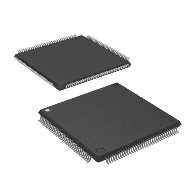


 工商网监
湘ICP备2023018690号
工商网监
湘ICP备2023018690号
