FullFlex
FullFlex™ Synchronous
DDR Dual-Port SRAM
Features
• True dual-ported memory allows simultaneous access
to the shared array from each port
• Synchronous pipelined operation with selectable
Double Data Rate (DDR) or Single Data Rate (SDR)
operation on each port
— DDR interface at 200 MHz
— Burst counters for sequential memory access
— Mailbox with interrupt flags for message passing
— Dual Chip Enables for easy depth expansion
Functional Description
— SDR interface at 250 MHz
— Up to 36-Gb/s bandwidth (250 MHz * 72 bit * 2 ports)
• Selectable pipelined or flow-through mode
• 1.5V or 1.8V core power supply
• Commercial and Industrial temperature ranges
• IEEE 1149.1 JTAG boundary scan
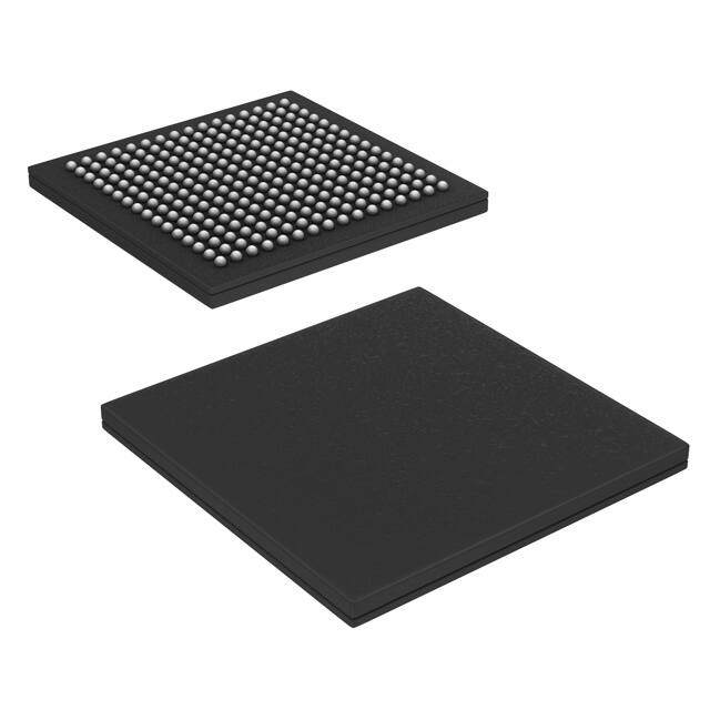
• Available in 484-ball PBGA Packages and 256-ball
FBGA Packages
• FullFlex72 family
— 18 Mbit: 256K x 36 x 2 DDR or 256K x 72 SDR
(CYDD18S72V18)
— 9 Mbit: 128K x 36 x 2 DDR or 128K x 72 SDR
(CYDD09S72V18)
— 4 Mbit: 64K x 36 x 2 DDR or 64 x 72 SDR
(CYDD04S72V18)
• FullFlex36 family
— 36 Mbit: 512K x 36 x 2 DDR (CYDD36S36V18)
— 18 Mbit: 256K x 36 x 2 DDR (CYDD18S36V18)
— 9 Mbit: 128K x 36 x 2 DDR (CYDD09S36V18)
— 4 Mbit: 64K x 36 x 2 DDR (CYDD04S36V18)
• FullFlex18 family
— 36 Mbit: 1M x 18 x 2 DDR (CYDD36S18V18)
— 18 Mbit: 512K x 18 x 2 DDR (CYDD18S18V18)
— 9 Mbit: 256K x 18 x 2 DDR (CYDD09S18V18)
— 4 Mbit: 128K x 18 x 2 DDR (CYDD04S18V18)
• Built-in deterministic access control to manage
address collisions
— Deterministic flag output upon collision detection
— Collision detection on back-to-back clock cycles
— First Busy Address readback
• Advanced features for improved high-speed data
transfer and flexibility
— Variable Impedance Matching (VIM)
— Echo clocks
Cypress Semiconductor Corporation
Document #: 38-06072 Rev. *I
— Selectable LVTTL (3.3V), Extended HSTL
(1.4V–1.9V), 1.8V LVCMOS, or 2.5V LVCMOS I/O on
each port
The FullFlex™ Dual-Port SRAM families consist of 4-Mbit,
9-Mbit, 18-Mbit, and 36-Mbit synchronous, true dual-port static
RAMs that are high-speed, low-power 1.8V/1.5V CMOS. Two
ports are provided, allowing the array to be accessed simultaneously. Simultaneous access to a location triggers deterministic access control. For FullFlex72, these ports can operate
independently in DDR mode with 36-bit bus widths or in SDR
mode with 72-bit bus widths. For FullFlex36 and FullFlex18,
the ports operate in DDR mode only. Each port can be
independently configured for two pipelined stages for SDR
mode or 2.5 stages in DDR mode. Each port can also be
configured to operate in pipelined or flow-through mode in
SDR mode.
Advanced features include built-in deterministic access
control to manage address collisions during simultaneous
access to the same memory location, Variable Impedance
Matching (VIM) to improve data transmission by matching the
output driver impedance to the line impedance, and echo
clocks to improve data transfer.
To reduce the static power consumption, chip enables can be
used to power down the internal circuitry. The number of
cycles of latency before a change in CE0 or CE1 will enable
or disable the databus matches the number of cycles of read
latency selected for the device. In order for a valid write or read
to occur, both chip enable inputs on a port must be active.
Each port contains an optional burst counter on the input
address register. After externally loading the counter with the
initial address, the counter will increment the address internally.
Additional features of this device include a mask register and
a mirror register to control counter increments and
wrap-around. The counter-interrupt (CNTINT) flags notify the
host that the counter will reach maximum count value on the
next clock cycle. The host can read the burst-counter internal
address, mask register address, and busy address on the
address lines. The host can also load the counter with the
address stored in the mirror register by utilizing the retransmit
functionality. Mailbox interrupt flags can be used for message
passing, and JTAG boundary scan and asynchronous Master
Reset (MRST) are also available. The logic block diagram in
Figure 1 displays these features.
The FullFlex72 DDR family of devices is offered in a 484-ball
plastic BGA package. The FullFlex36 and FullFlex18 DDR
only families of devices are offered in both 484-ball and
256-ball fine pitch BGA packages.
•
198 Champion Court
•
San Jose, CA 95134-1709
•
408-943-2600
Revised December 21, 2006
[+] Feedback
�FullFlex
FTSELL
FTSELR
CQENL
CQENR
PORTSTD[1:0]L
CONFIG Block
CONFIG Block
PORTSTD[1:0]R
DDRONL
DDRONR
DQ[71:0]L
BE [7:0]L
CE0L
CE1L
OEL
IO
Control
DQ [71:0]R
BE [7:0]R
CE0R
CE1R
OER
IO
Control
R/WR
CQ0R
CQ0R
CQ1R
CQ1R
R/WL
CQ0L
CQ0L
CQ1L
CQ1L
Dual Ported Array
Collision Detection
Logic
BUSYL
A [19:0]L
CNT/MSKL
ADSL
CNTENL
CNTRSTL
RETL
CNTINTL
CL
CL
WRPL
Address &
Counter Logic
BUSYR
Address &
Counter Logic
A [19:0]R
CNT/MSKR
ADSR
CNTENR
CNTRSTR
RETR
CNTINTR
CR
CR
WRPR
Mailboxes
INTL
INTR
READYL
LowSPDL
ZQ0L
ZQ1L
JTAG
RESET
LOGIC
TRST
TMS
TDI
TDO
TCK
MRST
READYR
LowSPDR
ZQ0R
ZQ1R
Figure 1. Block Diagram[1,2,3]
Notes:
1. The CYDD36S18V18 device has 20 address bits. The CYDD36S36V18, and the CYDD18S18V18 devices have 19 address bits. The CYDD18S72V18,
CYDD18S36V18, and the CYDD09S18V18 devices have 18 address bits. The CYDD09S72V18, CYDD04S18V18, and the CYDD09S36V18 devices have 17
address bits. The CYDD04S36V18 and the CYDD04S72V18 devices have 16 address bits.
2. The FullFlex72 family of devices has 72 data lines. The FullFlex36 family of devices has 36 data lines. The FullFlex18 family of devices has 18 data lines.
3. The FullFlex72 family of devices has eight byte enables. The FullFlex36 family of devices has four byte enables. The FullFlex18 family of devices has two byte
enables.
Document #: 38-06072 Rev. *I
Page 2 of 53
[+] Feedback
�FullFlex
FullFlex72 SDR/DDR 484-ball BGA Pinout (Top View)
1
2
3
4
5
6
7
8
9
10
11
12
13
14
15
16
17
18
19
20
21
22
A
DNU DQ34 DQ32 DQ30 DQ27 DQ60 DQ57 DQ54 DQ24 DQ21 DQ18 DQ18 DQ21 DQ24 DQ54 DQ57 DQ60 DQ27 DQ30 DQ32 DQ34 DNU
L
L
L
L
L
L
L
L
L
L
R
R
R
R
R
R
R
R
R
R
B
DQ63 DQ35 DQ33 DQ31 DQ28 DQ61 DQ58 DQ55 DQ25 DQ22 DQ19 DQ19 DQ22 DQ25 DQ55 DQ58 DQ61 DQ28 DQ31 DQ33 DQ35 DQ63
L
L
L
L
L
L
L
L
L
L
L
R
R
R
R
R
R
R
R
R
R
R
C
DQ65 DQ64 VSS
L
L
VSS DQ29 DQ62 DQ59 DQ56 DQ26 DQ23 DQ20 DQ20 DQ23 DQ26 DQ56 DQ59 DQ62 DQ29 VSS
L
L
L
L
L
L
L
R
R
R
R
R
R
R
VSS DQ64 DQ65
R
R
DQ67 DQ66 VSS
L
L
VSS
VSS CQ1L CQ1L DDR LOW PORT ZQ0L BUSY CNTI PORT DNU CQ1R CQ1R VSS
ONL SPDL STD0 [4]
L
NTL STD1
L
L
VSS
VSS DQ66 DQ67
R
R
E
DQ69 DQ68 VDDI VSS
L
L
OL
VSS VDDI VDDI VDDI VDDI VDDI VTTL VTTL VTTL VDDI VDDI VDDI VDDI DNU
OL
OL
OL
OL
OL
OR
OR
OR
OR
VSS VDDI DQ68 DQ69
OR
R
R
F
DQ71 DQ70 CE1L CE0L VDDI VDDI VDDI VDDI VDDI VCO VCO VCO VCO VDDI VDDI VDDI VDDI VDDI CE0R CE1R DQ70 DQ71
L
L
OL
OL
OL
OL
OL
RE
RE
RE
RE
OR
OR
OR
OR
OR
R
R
D
A0L
A1L RETL BE2L VDDI VDDI VREF VSS
OL
OL
L
VSS
VSS
VSS
VSS
VSS
VSS
VSS VREF VDDI VDDI BE2R RETR A1R
R
OR
OR
A0R
A2L
A3L
WRP BE6L VDDI VDDI VSS
OL
OL
L
VSS
VSS
VSS
VSS
VSS
VSS
VSS
VSS
VSS VDDI VDDI BE6R WRP
OR
OR
R
A3R
A2R
A4L
A5L READ BE3L VDDI VDDI VSS
YL
OL
OL
VSS
VSS
VSS
VSS
VSS
VSS
VSS
VSS
VSS VDDI VDDI BE3R READ A5R
OR
OR
YR
A4R
A6L
A7L
VSS
VSS
VSS
VSS
VSS
VSS
VSS
VSS
VSS
VSS
VCO VDDI BE7R ZQ1R A7R
[4]
RE
OR
A6R
A8L
A9L
CL
OEL VTTL VCO
RE
VSS
VSS
VSS
VSS
VSS
VSS
VSS
VSS
VSS
VSS
VCO VTTL OER
RE
CR
A9R
A8R
A10L A11L
CL
BE5L VTTL VCO
RE
VSS
VSS
VSS
VSS
VSS
VSS
VSS
VSS
VSS
VSS
VCO VTTL BE5R
RE
CR
A11R A10R
A12L A13L ADSL BE1L VDDI VCO
OL
RE
VSS
VSS
VSS
VSS
VSS
VSS
VSS
VSS
VSS
VSS
VCO VTTL BE1R ADSR A13R A12R
RE
A14L A15L CNT/ BE4L VDDI VDDI VSS
OL
OL
MSKL
VSS
VSS
VSS
VSS
VSS
VSS
VSS
VSS
VSS VDDI VDDI BE4R CNT/ A15R A14R
OR
OR
MSK
R
R
A16L A17L CNTE BE0L VDDI VDDI VSS
[7]
[6]
OL
OL
NL
VSS
VSS
VSS
VSS
VSS
VSS
VSS
VSS
VSS VDDI VDDI BE0R CNTE A17R A16R
[6]
[7]
OR
OR
NR
T
A18L DNU CNTR INTL VDDI VDDI VREF VSS
[5]
STL
OL
OL
L
VSS
VSS
VSS
VSS
VSS
VSS
VSS VREF VDDI VDDI INTR CNTR DNU A18R
[5]
R
OR
OR
STR
U
DQ53 DQ52 R/WL CQE VDDI VDDI VDDI VDDI VDDI VCO VCO VCO VCO VDDI VDDI VDDI VDDI VDDI CQE R/WR DQ52 DQ53
L
L
NL
OL
OL
OL
OL
OL
RE
RE
RE
RE
OR
OR
OR
OR
OR
NR
R
R
V
DQ51 DQ50 FTSE VDDI DNU VDDI VDDI VDDI VDDI VTTL VTTL VTTL VDDI VDDI VDDI VDDI VDDI TRST VDDI FTSE DQ50 DQ51
L
L
OL
OL
OL
OL
OL
OR
OR
OR
OR
OR
OR
R
R
LL
LR
W
DQ49 DQ48 VSS MRST VSS CQ0L CQ0L DNU PORT CNTI BUSY ZQ0R PORT LOW DDR CQ0R CQ0R VSS
[4]
L
L
STD1 NTR
STD0 SPDR ONR
R
R
R
Y
DQ47 DQ46 VSS
L
L
G
H
J
K
L
M
N
P
ZQ1L BE7L VTTL VCO
[4]
RE
TDI
TDO DQ48 DQ49
R
R
VSS DQ11 DQ44 DQ41 DQ38 DQ8L DQ5L DQ2L DQ2R DQ5R DQ8R DQ38 DQ41 DQ44 DQ11 TMS
L
L
L
L
R
R
R
R
TCK DQ46 DQ47
R
R
AA
DQ45 DQ17 DQ15 DQ13 DQ10 DQ43 DQ40 DQ37 DQ7L DQ4L DQ1L DQ1R DQ4R DQ7R DQ37 DQ40 DQ43 DQ10 DQ13 DQ15 DQ17 DQ45
L
L
L
L
L
L
L
L
R
R
R
R
R
R
R
R
AB
DNU DQ16 DQ14 DQ12 DQ9L DQ42 DQ39 DQ36 DQ6L DQ3L DQ0L DQ0R DQ3R DQ6R DQ36 DQ39 DQ42 DQ9R DQ12 DQ14 DQ16 DNU
L
L
L
L
L
L
R
R
R
R
R
R
Notes:
4. Leaving this pin DNU disables VIM
5. Leave this ball unconnected for CYDD18S72V18, CYDD09S72V18 and CYDD04S72V18.
6. Leave this ball unconnected for CYDD09S72V18 and CYDD04S72V18
7. Leave this ball unconnected for CYDD04S72V18
Document #: 38-06072 Rev. *I
Page 3 of 53
[+] Feedback
�FullFlex
FullFlex36 DDR 484-ball BGA Pinout (Top View)[8]
1
2
3
4
5
6
7
8
9
10
11
12
13
14
15
16
17
18
19
20
21
22
A
DNU DNU DNU DNU DNU DQ33 DQ30 DQ27 DQ24 DQ21 DQ18 DQ18 DQ21 DQ24 DQ27 DQ30 DQ33 DNU DNU DNU DNU DNU
L
L
L
L
L
L
R
R
R
R
R
R
B
DNU DNU DNU DNU DNU DQ34 DQ31 DQ28 DQ25 DQ22 DQ19 DQ19 DQ22 DQ25 DQ28 DQ31 DQ34 DNU DNU DNU DNU DNU
L
L
L
L
L
L
R
R
R
R
R
R
DNU DNU
VSS
VSS
DNU DQ35 DQ32 DQ29 DQ26 DQ23 DQ20 DQ20 DQ23 DQ26 DQ29 DQ32 DQ35 DNU
L
L
L
L
L
L
R
R
R
R
R
R
VSS
VSS
DNU DNU
DNU DNU
VSS
VSS
VSS CQ1L CQ1L VDDI LOW PORT ZQ0L BUSY CNTI PORT DNU CQ1R CQ1R VSS
OL SPDL STD0 [4]
L
NTL STD1
L
L
VSS
VSS
DNU DNU
E
DNU DNU VDDI VSS
OL
VSS VDDI VDDI VDDI VDDI VDDI VTTL VTTL VTTL VDDI VDDI VDDI VDDI DNU
OL
OR
OR
OR
OR
OL
OL
OL
OL
VSS VDDI DNU DNU
OR
F
DNU DNU CE1L CE0L VDDI VDDI VDDI VDDI VDDI VCO VCO VCO VCO VDDI VDDI VDDI VDDI VDDI CE0R CE1R DNU DNU
OL
OL
OR
OR
OR
RE
RE
RE
RE
OL
OL
OL
OR
OR
C
D
A0L
A1L RETL BE2L VDDI VDDI VREF VSS
OL
OL
L
VSS
VSS
VSS
VSS
VSS
VSS
VSS VREF VDDI VDDI BE2R RETR A1R
R
OR
OR
A0R
A2L
A3L
WRP BE3L VDDI VDDI VSS
OL
OL
L
VSS
VSS
VSS
VSS
VSS
VSS
VSS
VSS
VSS VDDI VDDI BE3R WRP
OR
OR
R
A3R
A2R
A4L
A5L READ DNU VDDI VDDI VSS
OL
OL
YL
VSS
VSS
VSS
VSS
VSS
VSS
VSS
VSS
VSS VDDI VDDI DNU READ A5R
OR
OR
YR
A4R
A6L
A7L
VSS
VSS
VSS
VSS
VSS
VSS
VSS
VSS
VSS
VSS
VCO VDDI DNU ZQ1R A7R
[4]
RE
OR
A6R
A8L
A9L
CL
OEL VTTL VCO
RE
VSS
VSS
VSS
VSS
VSS
VSS
VSS
VSS
VSS
VSS
VCO VTTL OER
RE
CR
A9R
A8R
A10L A11L
CL
DNU VTTL VCO
RE
VSS
VSS
VSS
VSS
VSS
VSS
VSS
VSS
VSS
VSS
VCO VTTL DNU
RE
CR
A11R A10R
A12L A13L ADSL DNU VDDI VCO
OL
RE
VSS
VSS
VSS
VSS
VSS
VSS
VSS
VSS
VSS
VSS
VCO VTTL DNU ADSR A13R A12R
RE
A14L A15L CNT/ BE1L VDDI VDDI VSS
OL
OL
MSKL
VSS
VSS
VSS
VSS
VSS
VSS
VSS
VSS
VSS VDDI VDDI BE1R CNT/ A15R A14R
OR
OR
MSK
R
R
A16L A17L CNTE BE0L VDDI VDDI VSS
OL
OL
NL
VSS
VSS
VSS
VSS
VSS
VSS
VSS
VSS
VSS VDDI VDDI BE0R CNTE A17R A16R
OR
OR
NR
T
A18L DNU CNTR INTL VDDI VDDI VREF VSS
OL
OL
L
STL
VSS
VSS
VSS
VSS
VSS
VSS
VSS VREF VDDI VDDI INTR CNTR DNU A18R
R
OR
OR
STR
U
DNU DNU R/WL CQE VDDI VDDI VDDI VDDI VDDI VCO VCO VCO VCO VDDI VDDI VDDI VDDI VDDI CQE R/WR DNU DNU
NL
OL
OL
OR
OR
OR
RE
RE
RE
RE
OL
OL
OL
OR
OR
NR
V
DNU DNU VDDI VDDI DNU VDDI VDDI VDDI VDDI VTTL VTTL VTTL VDDI VDDI VDDI VDDI VDDI TRST VDDI VDDI DNU DNU
OL
OL
OR
OR
OR
OR
OL
OL
OL
OL
OR
OR
OR
G
H
J
K
L
M
N
P
DNU DNU
VSS MRST VSS CQ0L CQ0L DNU PORT CNTI BUSY ZQ0R PORT LOW VDDI CQ0R CQ0R VSS
[4]
STD1 NTR
R
STD0 SPDR OR
R
R
TDI
TDO
DNU DNU
DNU DNU
VSS
TMS
TCK
DNU DNU
W
Y
ZQ1L DNU VTTL VCO
[4]
RE
VSS
DNU DQ17 DQ14 DQ11 DQ8L DQ5L DQ2L DQ2R DQ5R DQ8R DQ11 DQ14 DQ17 DNU
L
L
L
R
R
R
AA
DNU DNU DNU DNU DNU DQ16 DQ13 DQ10 DQ7L DQ4L DQ1L DQ1R DQ4R DQ7R DQ10 DQ13 DQ16 DNU DNU DNU DNU DNU
L
L
L
R
R
R
AB
DNU DNU DNU DNU DNU DQ15 DQ12 DQ9L DQ6L DQ3L DQ0L DQ0R DQ3R DQ6R DQ9R DQ12 DQ15 DNU DNU DNU DNU DNU
L
L
R
R
Note:
8. Use this pinout only for device CYDD36S36V18 of the FullFlex36 family.
Document #: 38-06072 Rev. *I
Page 4 of 53
[+] Feedback
�FullFlex
FullFlex18 DDR 484-ball BGA Pinout (Top View)[9]
1
2
3
4
5
6
7
8
9
10
11
12
13
14
15
16
17
18
19
20
21
22
A
DNU DNU DNU DNU DNU DNU DNU DNU DQ15 DQ12 DQ9L DQ9R DQ12 DQ15 DNU DNU DNU DNU DNU DNU DNU DNU
L
L
R
R
B
DNU DNU DNU DNU DNU DNU DNU DNU DQ16 DQ13 DQ10 DQ10 DQ13 DQ16 DNU DNU DNU DNU DNU DNU DNU DNU
L
L
L
R
R
R
DNU DNU
VSS
VSS
DNU DNU DNU DNU DQ17 DQ14 DQ11 DQ11 DQ14 DQ17 DNU DNU DNU DNU
L
L
L
R
R
R
VSS
VSS
DNU DNU
DNU DNU
VSS
VSS
VSS CQ1L CQ1L VDDI LOW PORT ZQ0L BUSY CNTI PORT DNU CQ1R CQ1R VSS
OL SPDL STD0 [4]
L
NTL STD1
L
L
VSS
VSS
DNU DNU
E
DNU DNU VDDI VSS
OL
VSS VDDI VDDI VDDI VDDI VDDI VTTL VTTL VTTL VDDI VDDI VDDI VDDI DNU
OL
OR
OR
OR
OR
OL
OL
OL
OL
VSS VDDI DNU DNU
OR
F
DNU DNU CE1L CE0L VDDI VDDI VDDI VDDI VDDI VCO VCO VCO VCO VDDI VDDI VDDI VDDI VDDI CE0R CE1R DNU DNU
OL
OL
OR
OR
OR
RE
RE
RE
RE
OL
OL
OL
OR
OR
C
D
A0L
A1L RETL BE1L VDDI VDDI VREF VSS
OL
OL
L
VSS
VSS
VSS
VSS
VSS
VSS
VSS VREF VDDI VDDI BE1R RETR A1R
R
OR
OR
A0R
A2L
A3L
WRP DNU VDDI VDDI VSS
OL
OL
L
VSS
VSS
VSS
VSS
VSS
VSS
VSS
VSS
VSS VDDI VDDI DNU WRP
OR
OR
R
A3R
A2R
A4L
A5L READ DNU VDDI VDDI VSS
YL
OL
OL
VSS
VSS
VSS
VSS
VSS
VSS
VSS
VSS
VSS VDDI VDDI DNU READ A5R
OR
OR
YR
A4R
A6L
A7L
VSS
VSS
VSS
VSS
VSS
VSS
VSS
VSS
VSS
VSS
VCO VDDI DNU ZQ1R A7R
[4]
RE
OR
A6R
A8L
A9L
CL
OEL VTTL VCO
RE
VSS
VSS
VSS
VSS
VSS
VSS
VSS
VSS
VSS
VSS
VCO VTTL OER
RE
CR
A9R
A8R
A10L A11L
CL
DNU VTTL VCO
RE
VSS
VSS
VSS
VSS
VSS
VSS
VSS
VSS
VSS
VSS
VCO VTTL DNU
RE
CR
A11R A10R
A12L A13L ADSL DNU VDDI VCO
OL
RE
VSS
VSS
VSS
VSS
VSS
VSS
VSS
VSS
VSS
VSS
VCO VTTL DNU ADSR A13R A12R
RE
A14L A15L CNT/ DNU VDDI VDDI VSS
OL
OL
MSKL
VSS
VSS
VSS
VSS
VSS
VSS
VSS
VSS
VSS VDDI VDDI DNU CNT/ A15R A14R
OR
OR
MSK
R
R
A16L A17L CNTE BE0L VDDI VDDI VSS
OL
OL
NL
VSS
VSS
VSS
VSS
VSS
VSS
VSS
VSS
VSS VDDI VDDI BE0R CNTE A17R A16R
OR
OR
NR
T
A18L A19L CNTR INTL VDDI VDDI VREF VSS
STL
OL
OL
L
VSS
VSS
VSS
VSS
VSS
VSS
VSS VREF VDDI VDDI INTR CNTR A19R A18R
R
OR
OR
STR
U
DNU DNU R/WL CQE VDDI VDDI VDDI VDDI VDDI VCO VCO VCO VCO VDDI VDDI VDDI VDDI VDDI CQE R/WR DNU DNU
NL
OL
OL
OR
OR
OR
RE
RE
RE
RE
OL
OL
OL
OR
OR
NR
V
DNU DNU VDDI VDDI DNU VDDI VDDI VDDI VDDI VTTL VTTL VTTL VDDI VDDI VDDI VDDI VDDI TRST VDDI VDDI DNU DNU
OL
OL
OR
OR
OR
OR
OL
OL
OL
OL
OR
OR
OR
G
H
J
K
L
M
N
P
DNU DNU
VSS MRST VSS CQ0L CQ0L DNU PORT CNTI BUSY ZQ0R PORT LOW VDDI CQ0R CQ0R VSS
[4]
STD1 NTR
STD0 SPDR OR
R
R
R
TDI
TDO
DNU DNU
DNU DNU
VSS
TMS
TCK
DNU DNU
W
Y
ZQ1L DNU VTTL VCO
[4]
RE
VSS
DNU DNU DNU DNU DQ8L DQ5L DQ2L DQ2R DQ5R DQ8R DNU DNU DNU DNU
AA
DNU DNU DNU DNU DNU DNU DNU DNU DQ7L DQ4L DQ1L DQ1R DQ4R DQ7R DNU DNU DNU DNU DNU DNU DNU DNU
AB
DNU DNU DNU DNU DNU DNU DNU DNU DQ6L DQ3L DQ0L DQ0R DQ3R DQ6R DNU DNU DNU DNU DNU DNU DNU DNU
Note:
9. Use this pinout only for device CYDD36S18V18 of the FullFlex18 family.
Document #: 38-06072 Rev. *I
Page 5 of 53
[+] Feedback
�FullFlex
FullFlex36 DDR 256 Ball BGA (Top View)
1
2
3
4
5
6
7
8
A
DQ32L
DQ30L
DQ28L
DQ26L
DQ24L
DQ22L
DQ20L
DQ18L
B
DQ33L
DQ31L
DQ29L
DQ27L
DQ25L
DQ23L
DQ21L
C
DQ34L
DQ35L
RETL
INTL
CQ1L
CQ1L
D
A0L
A1L
WRPL
E
A2L
A3L
CE0L
CE1L
VDDIOL VDDIOL VDDIOL VCORE
F
A4L
A5L
CNTINTL
BE3L
VDDIOL VDDIOL
VSS
G
A6L
A7L
BUSYL
BE2L
ZQ0L[4]
VSS
H
A8L
A9L
CL
VTTL
VCORE
J
A10L
A11L
CL
PORTS VCORE
TD1L
K
A12L
A13L
OEL
BE1L
L
A14L
A15L
ADSL
BE0L
M
A16L[11] A17L[10]
R/WL
N
DNU
DNU
P
DQ16L
DQ17L
R
DQ15L
DQ13L
DQ11L
T
DQ14L
DQ12L
DQ10L
11
12
13
14
15
16
DQ18R DQ20R
DQ22R
DQ24R
DQ26R
DQ28R
DQ30R
DQ32R
DQ19L
DQ19R DQ21R
DQ23R
DQ25R
DQ27R
DQ29R
DQ31R
DQ33R
DNU
TRST
MRST
ZQ0R[4]
CQ1R
CQ1R
INTR
RETR
DQ35R
DQ34R
VSS
VTTL
VTTL
VSS
LOWSP
DR
VDDIO
R
VREFR
WRPR
A1R
A0R
VCOR
E
VDDIO
R
VDDIO
R
VDDIO
R
CE1R
CE0R
A3R
A2R
VSS
VSS
VSS
VSS
VDDIO
R
BE3R
CNTINT
R
A5R
A4R
VSS
VSS
VSS
VSS
VSS
VDDIO
R
BE2R
BUSYR
A7R
A6R
VSS
VSS
VSS
VSS
VSS
VSS
VCORE
VTTL
CR
A9R
A8R
VSS
VSS
VSS
VSS
VSS
VSS
VCORE PORTS
TD1R
CR
A11R
A10R
VDDIOL
VSS
VSS
VSS
VSS
VSS
VSS
VDDIO
R
BE1R
OER
A13R
A12R
VDDIOL
VSS
VSS
VSS
VSS
VSS
VDDIO
R
VDDIO
R
BE0R
ADSR
A15R
A14R
VCOR
E
VDDIO
R
VDDIO
R
VDDIO
R
CQENR
R/WR
ZQ1R[4] READY PORTS
R
TD0R
VREFR
CNT/MS
KR
VREFL VDDIOL LOWSP
DL
CQENL VDDIOL VDDIOL VDDIOL VCORE
CNT/MS VREFL PORTS READY
KL
TD0L
L
CNTENL CNTRS
TL
9
ZQ1L[4]
VTTL
VTTL
10
A17R[10] A16R[11]
DNU
CNTRS CNTENR DQ17R
TR
DNU
CQ0L
CQ0L
TCK
TMS
TDO
TDI
CQ0R
CQ0R
DQ16R
DQ9L
DQ7L
DQ5L
DQ3L
DQ1L
DQ1R
DQ3R
DQ5R
DQ7R
DQ9R
DQ11R
DQ13R
DQ15R
DQ8L
DQ6L
DQ4L
DQ2L
DQ0L
DQ0R
DQ2R
DQ4R
DQ6R
DQ8R
DQ10R
DQ12R
DQ14R
Notes:
10. Leave this ball unconnected for CYDD09S36V18 and CYDD04S36V18.
11. Leave this ball unconnected for CYDD04S36V18.
Document #: 38-06072 Rev. *I
Page 6 of 53
[+] Feedback
�FullFlex
FullFlex18 DDR 256 Ball BGA (Top View)
1
2
3
4
5
6
7
8
9
10
11
12
13
14
15
16
A
DNU
DNU
DNU
DQ17L
DQ16L
DQ13L
DQ12L
DQ9L
DQ9R
DQ12R
DQ13R
DQ16R
DQ17R
DNU
DNU
DNU
B
DNU
DNU
DNU
DNU
DQ15L
DQ14L
DQ11L
DQ10L
DQ10R
DQ11R
DQ14R
DQ15R
DNU
DNU
DNU
DNU
C
DNU
DNU
RETL
INTL
CQ1L
CQ1L
DNU
TRST
MRST
ZQ0R[4]
CQ1R
CQ1R
INTR
RETR
DNU
DNU
D
A0L
A1L
WRPL
VSS
VTTL
VTTL
VSS
WRPR
A1R
A0R
E
A2L
A3L
CE0L
CE1L
VDDIOL VDDIOL VDDIOL VCORE VCORE VDDIOR VDDIOR VDDIOR
CE1R
CE0R
A3R
A2R
F
A4L
A5L
CNTINTL
DNU
VDDIOL VDDIOL
VSS
VSS
VSS
VSS
VSS
VDDIOR
DNU
CNTINTR
A5R
A4R
G
A6L
A7L
BUSYL
DNU
ZQ0L[4]
VSS
VSS
VSS
VSS
VSS
VSS
VDDIOR
DNU
BUSYR
A7R
A6R
H
A8L
A9L
CL
VTTL
VCORE
VSS
VSS
VSS
VSS
VSS
VSS
VCORE
VTTL
CR
A9R
A8R
J
A10L
A11L
CL
PORTST VCORE
D1L
VSS
VSS
VSS
VSS
VSS
VSS
VCORE PORTST
D1R
CR
A11R
A10R
K
A12L
A13L
OEL
BE1L
VDDIOL
VSS
VSS
VSS
VSS
VSS
VSS
VDDIOR
BE1R
OER
A13R
A12R
L
A14L
A15L
ADSL
BE0L
VDDIOL
VSS
VSS
VSS
VSS
VSS
VDDIOR VDDIOR
BE0R
ADSR
A15R
A14R
M
A16L
A17L[13]
R/WL
R/WR
A17R[13]
A16R
N
A18L[12]
DNU
CNT/MS VREFL PORTST READYL ZQ1L[4]
KL
D0L
VTTL
VTTL
DNU
A18R[12]
P
DNU
DNU
CNTENL CNTRST
L
DNU
DNU
R
DNU
DNU
DNU
T
DNU
DNU
DNU
VREFL VDDIOL LOWSP
DL
LOWSP VDDIOR VREFR
DR
CQENL VDDIOL VDDIOL VDDIOL VCORE VCORE VDDIOR VDDIOR VDDIOR CQENR
ZQ1R[4] READY PORTST VREFR CNT/MS
R
D0R
KR
CQ0L
CQ0L
TCK
TMS
TDO
TDI
CQ0R
CQ0R
CNTRST CNTENR
R
DNU
DQ6L
DQ5L
DQ2L
DQ1L
DQ1R
DQ2R
DQ5R
DQ6R
DNU
DNU
DNU
DNU
DQ8L
DQ7L
DQ4L
DQ3L
DQ0L
DQ0R
DQ3R
DQ4R
DQ7R
DQ8R
DNU
DNU
DNU
Table 1. Selection Guide
–200
–167
Unit
SDR fMAX[14]
DDR fMAX[15]
250
200
MHz
200
167
MHz
SDR Max. Access Time (Clock to Data)
2.64
3.3
ns
DDR Max. Access Time (Clock to Data)
0.50
0.60
ns
Typical Operating Current ICC
800[16]
700[16]
mA
Typical Standby Current for ISB3 (Both Ports CMOS Level)
210[16]]
210[16]
mA
Notes:
12. Leave this ball unconnected for CYDD09S18V18 and CYDD04S18V18.
13. Leave this ball unconnected for CYDD04S18V18.
14. SDR mode with two pipelined stages.
15. DDR mode with 2.5 pipelined stages.
16. For 18-Mbit x36x2 DDR commercial configuration only, please refer to the electrical characteristics section for complete information.
Document #: 38-06072 Rev. *I
Page 7 of 53
[+] Feedback
�FullFlex
Pin Definitions
Left Port
Right Port
Description
A[19:0]L
A[19:0]R
Address Inputs.[1]
DQ[71:0]L
DQ[71:0]R
Data Bus Input/Output.[2]
BE[7:0]L
BE[7:0]R
Byte Select Inputs.[3] Asserting these signals enables Read and Write operations to the
corresponding bytes of the memory array.
BUSYL
BUSYR
Port Busy Output. When there is an address match and both chip enables are active for
both ports, an external BUSY signal is asserted on the fifth clock cycle from when the collision
occurs.
C/CL
C/CR
Clock Signal.[18] Maximum clock input rate is fMAX. Tie C to VSS when operating in SDR
mode.
CE0L
CE0R
Active LOW Chip Enable Input.
CE1L
CE1R
Active HIGH Chip Enable Input.
CQENL
CQENR
Echo Clock Enable Input. Assert HIGH to enable echo clocking on respective port.
CQ0L
CQ0R
Echo Clock Signal Output for DQ[35:0] for FullFlex72 devices. Echo Clock Signal Output
for DQ[17:0] for FullFlex36 devices. Echo Clock Signal Output for DQ[8:0] for FullFlex18
devices.
CQ0L
CQ0R
Inverted Echo Clock Signal Output for DQ[35:0] for FullFlex72 devices. Inverted Echo
Clock Signal Output for DQ[17:0] for FullFlex36 devices. Inverted Echo Clock Signal Output
for DQ[8:0] for FullFlex18 devices.
CQ1L
CQ1R
Echo Clock Signal Output for DQ[71:36] for FullFlex72 devices. Echo Clock Signal
Output for DQ[35:18] for FullFlex36 devices. Echo Clock Signal Output for DQ[17:9] for
FullFlex18 devices.
CQ1L
CQ1R
Inverted Echo Clock Signal Output for DQ[71:36] for FullFlex72 devices. Inverted Echo
Clock Signal Output for DQ[35:18] for FullFlex36 devices. Inverted Echo Clock Signal Output
for DQ[17:9] forFullFlex18 devices.
DDRONL[17]
DDRONR[17]
DDR Enable Input. Assert HIGH to enable DDR clocking on respective port.
ZQ[1:0]L
ZQ[1:0]R
VIM Output Impedance Matching Input. To use, connect a calibrating resistor between ZQ
and ground. The resistor must be five times larger than the intended line impedance driven
by the dual-port. Assert HIGH or leave DNU to disable Variable Impedance Matching.
OEL
OER
Output Enable Input. This asynchronous signal must be asserted LOW to enable the DQ
data pins during Read operations.
INTL
INTR
Mailbox Interrupt Flag Output. The mailbox permits communications between ports. The
upper two memory locations can be used for message passing. INTL is asserted LOW when
the right port writes to the mailbox location of the left port, and vice versa. An interrupt to a
port is deasserted HIGH when it reads the contents of its mailbox.
LowSPDL
LowSPDR
Port Low Speed Select Input. Assert this pin LOW to disable the DLL. For operation at less
than 100 MHz, assert this pin LOW.
PORTSTD[1:0]L PORTSTD[1:0]R Port Clock/Address/Control/Data/Echo Clock/I/O Standard Select Input. Assert these
[19]
[19]
pins LOW/LOW for LVTTL, LOW/HIGH for HSTL, HIGH/LOW for 2.5V LVCMOS, and
HIGH/HIGH for 1.8V LVCMOS, respectively. These pins must be driven by VTTL referenced
levels.
R/WL
R/WR
Read/Write Enable Input. Assert this pin LOW to Write to, or HIGH to Read from the
dual-port memory array.
READYL
READYR
Port DLL Ready Output. This signal will be asserted LOW when the DLL and Variable
Impedance Matching circuits have completed calibration. This is a wired OR capable output.
CNT/MSKL
CNT/MSKR
Port Counter/Mask Select Input. Counter control input.
ADSL
ADSR
Port Counter Address Load Strobe Input. Counter control input.
CNTENL
CNTENR
Port Counter Enable Input. Counter control input.
Notes:
17. DDRONL and DDRONR needs to tie to the same voltage level for FullFlex36 and FullFlex18 Family.
18. C and C are complimentary for DDR operation.
19. PORTSTD[1:0]L and PORTSTD[1:0]R have internal pull-down resistors.
Document #: 38-06072 Rev. *I
Page 8 of 53
[+] Feedback
�FullFlex
Pin Definitions (continued)
Left Port
Right Port
Description
CNTRSTL
CNTRSTR
Port Counter Reset Input. Counter control input.
CNTINTL
CNTINTR
Port Counter Interrupt Output. This pin is asserted LOW one cycle before the unmasked
portion of the counter is incremented to all “1s”.
WRPL
WRPR
Port Counter Wrap Input. When the burst counter reaches the maximum count, on the next
counter increment WRP can be set LOW to load the unmasked counter bits to 0 or set HIGH
to load the counter with the value stored in the mirror register.
RETL
RETR
Port Counter Retransmit Input. Assert this pin LOW to reload the initial address for
repeated access to the same segment of memory.
VREFL
VREFR
Port External HSTL I/O Reference Input. This pin is left DNU when HSTL is not used.
VDDIOL
VDDIOR
Port Data I/O Power Supply.
FTSELL
FTSELR
Port Flow-through Mode Select Input. Assert this pin LOW to select Flow-through mode.
Assert this pin HIGH to select Pipelined mode. Selection for SDR only.
MRST
Master Reset Input. MRST is an asynchronous input signal and affects both ports. Asserting
MRST LOW performs all of the reset functions as described in the text. A MRST operation
is required at power-up. This pin must be driven by VDDIOL referenced levels.
TMS
JTAG Test Mode Select Input. It controls the advance of JTAG TAP state machine. State
machine transitions occur on the rising edge of TCK. Operation for LVTTL or 2.5V LVCMOS.
TDI
JTAG Test Data Input. Data on the TDI input will be shifted serially into selected registers.
Operation for LVTTL or 2.5V LVCMOS.
TRST
JTAG Reset Input. Operation for LVTTL or 2.5V LVCMOS.
TCK
JTAG Test Clock Input. Operation for LVTTL or 2.5V LVCMOS.
TDO
JTAG Test Data Output. TDO transitions occur on the falling edge of TCK. TDO is normally
three-stated except when captured data is shifted out of the JTAG TAP. Operation for LVTTL
or 2.5V LVCMOS.
VSS
Ground Inputs.
VCORE
Device Core Power Supply.
VTTL
LVTTL Power Supply.
Selectable I/O Standard
Clocking
The FullFlex device families also offer the option of choosing
one of four port standards for the device. Each port can
independently select standards from single-ended HSTL class
I, single-ended LVTTL, 2.5V LVCMOS, or 1.8V LVCMOS. The
selection of the standard is determined by the PORTSTD pins
for each port. These pins must be connected to a VTTL power
supply. This will determine the input clock, address, control,
data, and Echo clock standard for each port as shown in
Table 2. Please note that only 1.8V LVCMOS and HSTL are
supported for 4-Mbit, 9-Mbit, 18-Mbit devices running at
250MHz SDR, and for 36-Mbit devices running at 200 MHz
SDR.
Separate clocks synchronize the operations on each port.
Each port has two clock inputs C and C. In SDR mode only the
C input clock is used and C should be tied to VSS. In this
mode, all the transactions on the address, control, and data
will be on the C rising edge. In DDR mode, both C and C will
be used and these signals are complementary. In this mode,
all transactions on the address and control, except for the byte
enables, will occur on the C rising edge. Transactions on the
data input, output, and byte enables will be on the C and C
rising edges.
Table 2. Port Standard Selection
PORTSTD1
VSS
VSS
VTTL
VTTL
PORTSTD0
VSS
VTTL
VSS
VTTL
Document #: 38-06072 Rev. *I
I/O Standard
LVTTL
HSTL
2.5V LVCMOS
1.8V LVCMOS
Double Data Rate (DDR)
In DDR mode with a x36 bus width, the input data is sampled
on both edges of the input clock. During a write, on the rising
edge of C, the first 36 bits (DQ[71:36]) will be latched into a
register. On the rising edge of C, the next 36 bits (DQ[35:0])
will be latched into a register. During a read, the first 36 bits
are driven out first on the rising edge of C. The next 36 bits will
be driven out on the rising edge of C. The internal bus width of
the FullFlex72 family is still x72. All counter operation is based
upon the x72 word width. The DDR option is set on a per port
basis by the configuration of the DDRON pin. Table 3 shows
the data assignment for SDR and DDR configuration. The
column on the right (Data Pin Name) shows the pins on which
data is presented on the data lines.
Page 9 of 53
[+] Feedback
�FullFlex
Table 3. Data Pin Assignment for SDR and DDR Configuration
x72 SDR Mode
x36 DDR Mode
BE Pin Name for
DDR
BE Pin Name for
SDR
Data Pin Name
Related Rising Edge
Clock for Write
Related Rising Edge
Clock for Read
Data Pin
Name
BE[3]
BE[7]
DQ[71]
C
C
DQ[35]
BE[3]
BE[3]
DQ[35]
C
C
BE[3]
BE[7]
DQ[70]
C
C
BE[3]
BE[3]
DQ[34]
C
C
BE[3]
BE[7]
DQ[69]
C
C
BE[3]
BE[3]
DQ[33]
C
C
BE[3]
BE[7]
DQ[68]
C
C
BE[3]
BE[3]
DQ[32]
C
C
BE[3]
BE[7]
DQ[67]
C
C
BE[3]
BE[3]
DQ[31]
C
C
BE[3]
BE[7]
DQ[66]
C
C
BE[3]
BE[3]
DQ[30]
C
C
BE[3]
BE[7]
DQ[65]
C
C
BE[3]
BE[3]
DQ[29]
C
C
BE[3]
BE[7]
DQ[64]
C
C
BE[3]
BE[3]
DQ[28]
C
C
BE[3]
BE[7]
DQ[63]
C
C
BE[3]
BE[3]
DQ[27]
C
C
BE[2]
BE[6]
DQ[62]
C
C
BE[2]
BE[2]
DQ[26]
C
C
BE[2]
BE[6]
DQ[61]
C
C
BE[2]
BE[2]
DQ[25]
C
C
BE[2]
BE[6]
DQ[60]
C
C
BE[2]
BE[2]
DQ[24]
C
C
BE[2]
BE[6]
DQ[59]
C
C
BE[2]
BE[2]
DQ[23]
C
C
BE[2]
BE[6]
DQ[58]
C
C
BE[2]
BE[2]
DQ[22]
C
C
BE[2]
BE[6]
DQ[57]
C
C
BE[2]
BE[2]
DQ[21]
C
C
BE[2]
BE[6]
DQ[56]
C
C
BE[2]
BE[2]
DQ[20]
C
C
BE[2]
BE[6]
DQ[55]
C
C
BE[2]
BE[2]
DQ[19]
C
C
BE[2]
BE[6]
DQ[54]
C
C
BE[2]
BE[2]
DQ[18]
C
C
BE[1]
BE[5]
DQ[53]
C
C
BE[1]
BE[1]
DQ[17]
C
C
BE[1]
BE[5]
DQ[52]
C
C
BE[1]
BE[1]
DQ[16]
C
C
Document #: 38-06072 Rev. *I
DQ[34]
DQ[33]
DQ[32]
DQ[31]
DQ[30]
DQ[29]
DQ[28]
DQ[27]
DQ[26]
DQ[25]
DQ[24]
DQ[23]
DQ[22]
DQ[21]
DQ[20]
DQ[19]
DQ[18]
DQ[17]
DQ[16]
Page 10 of 53
[+] Feedback
�FullFlex
Table 3. Data Pin Assignment for SDR and DDR Configuration (continued)
x72 SDR Mode
BE Pin Name for
DDR
BE Pin Name for
SDR
BE[1]
x36 DDR Mode
Data Pin Name
Related Rising Edge
Clock for Write
Related Rising Edge
Clock for Read
Data Pin
Name
BE[5]
DQ[51]
C
C
DQ[15]
BE[1]
BE[1]
DQ[15]
C
C
BE[1]
BE[5]
DQ[50]
C
C
BE[1]
BE[1]
DQ[14]
C
C
BE[1]
BE[5]
DQ[49]
C
C
BE[1]
BE[1]
DQ[13]
C
C
BE[1]
BE[5]
DQ[48]
C
C
BE[1]
BE[1]
DQ[12]
C
C
BE[1]
BE[5]
DQ[47]
C
C
BE[1]
BE[1]
DQ[11]
C
C
BE[1]
BE[5]
DQ[46]
C
C
BE[1]
BE[1]
DQ[10]
C
C
BE[1]
BE[5]
DQ[45]
C
C
BE[1]
BE[1]
DQ[9]
C
C
BE[0]
BE[4]
DQ[44]
C
C
BE[0]
BE[0]
DQ[8]
C
C
BE[0]
BE[4]
DQ[43]
C
C
BE[0]
BE[0]
DQ[7]
C
C
BE[0]
BE[4]
DQ[42]
C
C
BE[0]
BE[0]
DQ[6]
C
C
BE[0]
BE[4]
DQ[41]
C
C
BE[0]
BE[0]
DQ[5]
C
C
BE[0]
BE[4]
DQ[40]
C
C
BE[0]
BE[0]
DQ[4]
C
C
BE[0]
BE[4]
DQ[39]
C
C
BE[0]
BE[0]
DQ[3]
C
C
BE[0]
BE[4]
DQ[38]
C
C
BE[0]
BE[0]
DQ[2]
C
C
BE[0]
BE[4]
DQ[37]
C
C
BE[0]
BE[0]
DQ[1]
C
C
BE[0]
BE[4]
DQ[36]
C
C
BE[0]
BE[0]
DQ[0]
C
C
DQ[14]
DQ[13]
DQ[12]
DQ[11]
DQ[10]
DQ[9]
DQ[8]
DQ[7]
DQ[6]
DQ[5]
DQ[4]
DQ[3]
DQ[2]
DQ[1]
DQ[0]
Selectable Pipelined/Flow-through Mode
DLL
To meet data rate and throughput requirements, the FullFlex
families offer selectable pipelined or flow-through mode.
Flow-through mode is only supported in the FullFlex72
devices when the port is configured in SDR mode. Echo clocks
are not supported in flow-through mode and the DLL must be
disabled.
The FullFlex families of devices have an on-chip DLL.
Enabling the DLL reduces the clock to data valid (tCD) time
allowing more setup time for the receiving device. For
operation at or below 100 MHz, the DLL must be disabled. This
is selectable by strapping LowSPD LOW.
Flow-through mode is selected by the FTSEL pin. Strapping
this pin HIGH selects pipelined mode. Strapping this pin LOW
selects flow-through mode.
Document #: 38-06072 Rev. *I
Whenever the operating frequency is altered beyond the Clock
Input Cycle to Cycle Jitter spec, the DLL is required to be reset
followed by 1024 clocks before any valid operation.
LowSPD pins can be used to reset the DLL(s) for a single port
independent of all other circuitry. MRST can be used to reset
Page 11 of 53
[+] Feedback
�FullFlex
all DLLs on the chip, for information on DLL lock and reset
time, please see the Master Reset section below.
Echo Clocking
As the speed of data increases, on-board delays caused by
parasitics make providing accurate clock trees extremely
difficult. To counter this problem, the FullFlex families incorporate Echo Clocks. Echo Clocks are enabled on a per port
basis. The dual-port receives input clocks (C and C for DDR
mode, C for SDR mode) that are used to clock in the address
and control signals for a read operation. The dual-port
retransmits the input clocks relative to the data output. The
buffered clocks are provided on the CQ1, CQ1, CQ0, and CQ0
outputs. Each port has two pairs of Echo clocks. Each clock is
associated with half the data bits. The output clock will match
the corresponding ports I/O configuration.
To enable Echo clock outputs, tie CQEN HIGH. To disable
Echo clock outputs, tie CQEN LOW.
Input Clock
Deterministic Access Control
Deterministic Access Control is provided for ease of design.
The circuitry detects when both ports are accessing the same
location and provides an external BUSY flag to the port on
which data may be corrupted. The collision detection logic
saves the address in conflict (Busy Address) to a readable
register. In the case of multiple collisions, the first Busy
address will be written to the Busy Address register.
If both ports are accessing the same location at the same time
and only one port is doing a write, if tCCS is met, then the data
being written to and read from the address is valid data. For
example, if the right port is reading and the left port is writing
and the left ports clock meets tCCS, then the data being read
from the address by the right port will be the old data. In the
same case, if the right ports clock meets tCCS, then the data
being read out of the address from the right port will be the new
data. In the above case, if tCCS is violated by the either ports
clock with respect to the other port and the right port gets the
external BUSY flag, the data from the right port is corrupted.
Table 4 shows the tCCS timing that must be met to guarantee
the data.
Table 5 shows that in the case of the left port writing and the
right port reading, when an external BUSY flag is asserted on
the right port, the data read out of the device will not be
guaranteed.
Data Out
Echo Clock
Echo Clock
Figure 2. SDR Echo Clock Delay
Input Clock
Input Clock
Data Out
Echo Clock
Echo Clock
Figure 3. DDR Echo Clock Delay
Document #: 38-06072 Rev. *I
The value in the busy address register can be read back to the
address lines. The required input control signals for this
function are shown in Table 8. The value in the busy address
register will be read out to the address lines tCA after the same
amount of latency as a data read operation in SDR mode. In
DDR mode, the address latency is only 2 cycles instead of 2.5
which is the data latency. After an initial address match, the
address under contention is saved in the busy address
register. All following address matches cause the BUSY flag
to be generated, however, none of the addresses are saved
into the busy address register. Once a busy readback is
performed, the address of the first match which happens at
least two clock cycles after the busy readback is saved into the
busy address register.
Page 12 of 53
[+] Feedback
�FullFlex
Table 4. tCCS Timing for All Operating Modes
Port A – Early Arriving Port Port B – Late Arriving Port
Mode
Active Edge
SDR
SDR
tCCS C/C Rise to Opposite C/C Rise Set-up Time
Mode
Active Edge
Unit
C
SDR
C
tCYC(min) – 0.5
ns
C
DDR
C
tCYC(min) – 0.5
ns
DDR
C
SDR
C
0.55 * tCYC + tCYC(min) – 1
ns
DDR
C
DDR
C
0.55 * tCYC + tCYC(min) – 1
ns
for Non-corrupt Data
Table 5. Deterministic Access Control Winning Port
Left Port
Read
Write
Read
Write
Right Port
Read
Read
Clock Timing
Left Clock
Right Clock
X
X
>tCCS
0
0
>tCCS
Write
Write
tCCS
Variable Impedance Matching (VIM)
Each port contains a Variable Impedance Matching circuit to
set the impedance of the I/O driver to match the impedance of
the on-board traces. The impedance is set for all outputs
except JTAG and is done on a per port basis. To take
advantage of the VIM feature, connect a calibrating resistor
(RQ) that is five times the value of the intended line impedance
from the ZQ pin to VSS. The output impedance is then
adjusted to account for drifts in supply voltage and temperature every 1024 clock cycles. If a port’s clock is suspended,
the VIM circuit will retain its last setting until the clock is
restarted. On restart, it will then resume periodic adjustment.
In the case of a significant change in device temperature or
supply voltage, recalibration will happen every 1024 clock
cycles. A Master Reset will initialize the VIM circuitry. Table 6
shows the VIM parameters and Table 7 describes the VIM
operation modes.
In order to disable VIM, the ZQ pin must be connected to
VDDIO of the relative supply for the I/Os before a Master
Reset.
BUSYL
H
H
H
BUSYR
H
H
H
H
H
H
H
H
H
H
L
H
L
L
L
H
H
L
H
L
H
H
H
H
H
H
L
H
L
Description
No Collision
Read OLD Data
Read NEW Data
Read OLD Data
Data Not Guaranteed
Read NEW Data
Data Not Guaranteed
Read NEW Data
Read OLD Data
Read NEW Data
Data Not Guaranteed
Read OLD Data
Data Not Guaranteed
Array Data Corrupted
Array Stores Right Port Data
Array Stores Left Port Data
Table 6. Variable Impedance Matching Parameters
Parameter
Min.
Max.
Unit
Tolerance
RQ Value
100
275
Ω
±2%
Output Impedance
20
55
Ω
±15%
Reset Time
N/A
1024
Cycles
N/A
Update Time
N/A
1024
Cycles
N/A
Table 7. Variable Impedance Matching Operation
RQ Connection
Output Configuration
100Ω–275Ω to
VSS
Output Driver Impedance = RQ/5 ± 15% at
Vout = VDDIO/2
ZQ to VDDIO
VIM Disabled. Rout < 20Ω at Vout =
VDDIO/2
Address Counter and Mask Register Operations[1]
Each port of the FullFlex families contains a programmable
burst address counter. The burst counter contains four
registers: a counter register, a mask register, a mirror register,
and a busy address register.
The counter register contains the address used to access the
RAM array. It is changed only by the master reset (MRST),
Counter Reset, Counter Load, Retransmit, and Counter
Increment operations.
Document #: 38-06072 Rev. *I
Page 13 of 53
[+] Feedback
�FullFlex
Counter Load Operation[1]
The mask register value affects the Counter Increment and
Counter Reset operations by preventing the corresponding
bits of the counter register from changing. It also affects the
counter interrupt output (CNTINT). The mask register is only
changed by Mask Reset, Mask Load, and MRST. The Mask
Load operation loads the value of the address bus into the
mask register. The mask register defines the counting range
of the counter register. The mask register is divided into two or
three consecutive regions. Zero or more “0s” define the
masked region and one or more “1s” define the unmasked
portion of the counter register. The counter register may only
be divided into up to three regions. The region containing the
least significant bits must be no more than two “0s”. Bits one
and zero may be “10” respectively, masking the least significant counter bit and causing the counter to increment by two
instead of one. If bits one and zero are “00”, the two least
significant bits are masked and the counter will increment by
four instead of one. For example, in the case of a 256Kx72
configuration, a mask register value of 003FC divides the
mask register into three regions. With bit 0 being the least
significant bit and bit 17 being the most significant bit, the two
least significant bits are masked, the next eight bits are
unmasked, and the remaining bits are masked.
The address counter and mirror registers are both loaded with
the address value presented on the address lines. This value
ranges from 0 to FFFFF.
Mask Load Operation[1]
The mask register is loaded with the address value presented
on the address bus. This value ranges from 0 to FFFFF though
not all values permit correct increment operations. Permitted
values are in the form of 2n–1, 2n–2, or 2n–4. The counter
register can only be segmented in up to three regions. From
the most significant bit to the least significant bit, permitted
values have zero or more “0s”, one or more “1s”, and the least
significant two bits can be “11”, “10”, or “00”. Thus FFFFE,
7FFFF, and 03FFC are permitted values but 2FFFF, 03FFA,
and 7FFE4 are not.
Counter Readback Operation
The internal value of the counter register can be read out on
the address lines. The address will be valid tCA after the
selected number of latency cycles configured by FTSEL. This
is the same as data in SDR mode and one half cycle earlier
than data latency for DDR mode. The data bus (DQ) is
tri-stated on the cycle that the address is presented on the
address lines. Figure 4 shows a block diagram of the logic.
The mirror register is used to reload the counter register on
retransmit operations (see “retransmit” below) and wrap
functions (see “counter increment” below). The last value
loaded into the counter register is stored in the mirror register.
The mirror register is only changed by master reset (MRST),
Counter Reset, and Counter Load.
Mask Readback Operation
The internal value of the mask register can be read out on the
address lines. The address will be valid tCA after the selected
number of latency cycles configured by FTSEL. For pipelined
SDR and DDR mode this is two cycles. The data bus (DQ) is
tri-stated on the cycle that the address is presented on the
address lines. Figure 4 shows a block diagram of the
operation.
Table 8 summarizes the operations of these registers and the
required input control signals. All signals except MRST are
synchronized to the ports clock.
Table 8. Burst Counter and Mask Register Control Operation (Any Port) [20,21]
C
X
MRST CNTRST CNT/MSK CNTEN ADS
RET
Operation
Description
L
X
X
X
X
X
Master Reset
Reset address counter to all 0s, mask register
to all 1s, and busy address to all 0’s.
H
L
H
X
X
X
Counter Reset
Reset counter and mirror unmasked portion to
all 0s.
H
L
L
X
X
X
Mask Reset
Reset mask register to all 1s.
H
H
H
L
L
X
Counter Load
Load burst counter and mirror with external
address value presented on address lines.
H
H
L
L
L
X
Mask Load
Load mask register with value presented on the
address lines.
H
H
H
L
H
L
Retransmit
Load counter with value in the mirror register
H
H
H
L
H
H
Counter
Increment
Internally increment address counter value.
H
H
H
H
H
H
Counter Hold
Constantly hold the address value for multiple
clock cycles.
H
H
H
H
L
H
Counter
Readback
Read out counter internal value on address
lines.
H
H
L
H
L
H
Mask Readback
Read out mask register value on address lines.
Notes:
20. X” = “Don’t Care”, “H” = HIGH, “L” = LOW.
21. Counter operation and mask register operation is independent of chip enables.
Document #: 38-06072 Rev. *I
Page 14 of 53
[+] Feedback
�FullFlex
Table 8. Burst Counter and Mask Register Control Operation (Any Port) (continued)[20,21]
C
MRST CNTRST CNT/MSK CNTEN ADS
RET
Operation
H
H
L
H
H
L
Busy Address
Readback
H
H
L
L
H
X
Reserved
H
H
L
H
L
L
Reserved
H
H
L
H
H
H
Reserved
H
H
H
H
L
L
Reserved
H
H
H
H
H
L
Reserved
Counter Reset Operation
All unmasked bits of the counter are reset to “0”. All masked
bits remain unchanged. The new burst counter value is loaded
into the mirror registers. A mask reset followed by a counter
reset will reset the counter and mirror registers to 00000.
Mask Reset Operation
The mask register is reset to all “1s”, which unmasks every bit
of the burst counter.
Increment Operation[1]
Once the address counter is initially loaded with an external
address, the counter can internally increment the address
value and address the entire memory array. Only the
unmasked bits of the counter register are incremented. In
order for a counter bit to change, the corresponding bit in the
mask register must be “1”. If the two least significant bits of the
mask register are “11”, the burst counter will increment by one.
If the two least significant bits are “10”, the burst counter will
increment by two, and if they are “00”, the burst counter will
increment by four. If all unmasked counter bits are incremented to “1” and WRP is deasserted, the next increment will
wrap the counter back to the initially loaded value. The cycle
before the increment that results in all unmasked counter bits
to become “1s”, a counter interrupt flag (CNTINT) is asserted
if the counter is incremented again. This increment will cause
the counter to reach its maximum value and the next increment
will return the counter register to its initial value that was stored
in the mirror register if WRP is deasserted. If WRP is asserted,
the unmasked portion of the counter is filled with “0” instead.
The example shown in Figure 5 shows an example of the
CYDD36S18V18 device with the mask register loaded with a
mask value of 0007F unmasking the seven least significant
bits. Setting the mask register to this value allows the counter
to access the entire memory space. The address counter is
then loaded with an initial value of 00005 assuming WRP is
deasserted. The base address bits (in this case, the seventh
address through the twentieth address) do not increment once
the counter is configured for increment operation. The counter
address will start at address 00005 and will increment its
internal address value until it reaches the mask register value
of 0007F. The counter wraps around the memory block to
location 00005 at the next count. CNTINT is issued when the
counter reaches the maximum –1 count.
Hold Operation
Description
Read out first busy address after last busy
address readback
operation is useful in applications where wait states are
needed, or when address is available a few cycles ahead of
data in a shared bus interface.
Retransmit
Retransmit allows repeated access to the same block of
memory without the need to reload the initial address. An
internal mirror register stores the address counter value last
loaded. While RET is asserted low, the counter will continue to
wrap back to the value in the mirror register independent of the
state of WRP.
Counter Interrupt
The counter interrupt (CNTINT) is asserted LOW one clock
cycle before an increment operation that results in the
unmasked portion of the counter register being all “1s”. It is
deasserted by counter reset, counter load, mask reset, mask
load, counter increment, re-transmit, and MRST.
Counting by Two
When the two least significant bits of the mask register are
“10,” the counter increments by two.
Counting by Four
When the two least significant bits of the mask register are
“00,” the counter increments by four.
Mailbox Interrupts
The upper two memory locations can be used for message
passing and permit communications between ports. Table 9
shows the interrupt operation for both ports. The highest
memory location is the mailbox for the right port and the
maximum address–1 is the mailbox for the left port.
When one port Writes to the other ports mailbox, the INT flag
of the port that the mailbox belongs to is asserted LOW. The
INT flag remains asserted until the mailbox location is read by
the other port. When a port reads it’s mailbox, the INT flag is
deasserted HIGH after one cycle of latency with respect to the
input clock of the port to which the mailbox belongs and is
independent of OE.
Table 9 shows that in order to set the INTR flag, a Write
operation by the left port to address FFFFF will assert INTR
LOW. A valid Read of the FFFFF location by the right port will
reset INTR HIGH after one cycle of latency with respect to the
The value of all three registers can be constantly maintained
unchanged for an unlimited number of clock cycles. Such
Document #: 38-06072 Rev. *I
Page 15 of 53
[+] Feedback
�FullFlex
right port’s clock. At least one byte enable has to be activated
to set or reset the mailbox interrupt.
CNT/MSK
CNTEN
Decode
Logic
A
CNTRST
RET
MRST
A
Mask
Register
Counter/
Address
Register
Address
Decode
RAM
Array
C
From
Address
Lines
Load / Increment
19
Mirror
From
Mask
Register
Increment
Logic
Wrap
19
From
Mask
From
Counter
19
To Readback
and Address
Decode
0
0
19
Counter
1
1
19
19
+1
+2
+4
Bit 0
and 1
Wrap
Detect
1
Wrap
0
1
19
To
Counter
0
Figure 4. Counter, Mask, and Mirror Logic Block Diagram[1]
Document #: 38-06072 Rev. *I
Page 16 of 53
[+] Feedback
�FullFlex
CNTINT
Example:
Load
Counter-Mask
H
Register = 00007F
0 0
0s
219 218
0
1 1 1
H
X X
Xs
219 218
Max
Address
Value
L
H
1
1
Unmasked Address
X
0 0 0
0
1
0
X X
Xs
X
1
1 1
1
Mask
Register
LSB
1
6
5
4
3 2
1
0
27 2 2 2 2 2 2 2
219 218
Max + 1
Address
Value
1
6
5
4
3 2
1
0
27 2 2 2 2 2 2 2
Masked Address
Load
Address
Counter = 000005
1
1 1
1
Address
Counter
LSB
6
5
4
3 2
1
0
27 2 2 2 2 2 2 2
X X
Xs
X
0 0
0
0
1 0
1
219 218
6
5
4
3 2
1
0
27 2 2 2 2 2 2 2
Figure 5. Programmable Counter-Mask Register Operation with WRP deasserted[1,25]
Table 9. Interrupt Operation Example [1, 20, 22, 23, 24]
Left Port
Function
R/WL
Right Port
CEL
A0L–19L
INTL
R/WR
CER
A0R–19R
INTR
Set Right INTR Flag
L
L
Max. Address
X
X
X
X
L
Reset Right INTR Flag
X
X
X
X
H
L
Max. Address
H
Set Left INTL Flag
X
X
X
L
L
L
Max. Address–1
X
Reset Left INTL Flag
H
L
Max. Address–1
H
X
X
X
X
Master Reset
The FullFlex family of dual-ports undergo a complete reset
when MRST is asserted. MRST must be driven by VDDIOL
referenced levels. The MRST can be asserted asynchronously
to the clocks and must remain asserted for at least tRS. Once
asserted MRST deasserts READY, initializes the internal burst
counters, internal mirror registers, and internal Busy
Addresses to zero, and initializes the internal mask register to
all “1s”. All mailbox interrupts (INT), Busy Address Outputs
(BUSY), and burst counter interrupts (CNTINT) are
deasserted upon master reset. Additionally, MRST must not
be released until all power supplies including VREF are fully
ramped, all port clocks and mode select inputs (LOWSPD, ZQ,
CQEN, DDRON, FTSEL, and PORTSTD) are valid and stable.
This begins calibration of the DLL and VIM circuits. READY
will be asserted within 1024 clock cycles. READY is a wired
OR capable output with a strong pull-up and weak pull-down.
Up to four outputs may be connected together. For faster
pull-down of the signal, connect a 250-Ω resistor to VSS. If the
DLL and VIM circuits are disabled for a port, the port will be
operational within five clock cycles. However, the READY will
be asserted within 160 clock cycles.
IEEE 1149.1 Serial Boundary Scan (JTAG)
The FullFlex families incorporate an IEEE 1149.1 serial
boundary scan test access port (TAP). The TAP operates
using JEDEC-standard 3.3V or 2.5V I/O logic levels depending
on the VTTL power supply. It is composed of four input
connections and one output connection required by the test
logic defined by the standard.
Notes:
22. CE is internal signal. CE = LOW if CE0 = LOW and CE1 = HIGH. For a single Read operation, CE only needs to be asserted once at the rising edge of the C and
can be deasserted after that. Data will be out after the following C edge and will be tri-stated after the next C edge.
23. OE is “Don’t Care” for mailbox operation.
24. At least one of BE0, BE1, BE2, BE3, BE4, BE5, BE6, or BE7 must be LOW.
25. The “X” in this diagram represents the counter’s upper bits.
Document #: 38-06072 Rev. *I
Page 17 of 53
[+] Feedback
�FullFlex
Table 10.JTAG IDCODE Register Definitions
Part Number
Table 11.Scan Registers Sizes
Configuration
Value
CYDD36S36V18
512Kx72
0C041069h
Instruction
Register Name
Bit Size
CYDD36S18V18
1024Kx36
0C042069h
Bypass
1
CYDD18S72V18
256Kx72
0C043069h
Identification
32
CYDD18S36V18
256Kx72
0C044069h
Boundary Scan
CYDD18S18V18
512Kx36
0C045069h
CYDD09S72V18
128Kx72
0C046069h
CYDD09S36V18
128Kx72
0C047069h
CYDD09S18V18
256Kx36
0C048069h
CYDD04S72V18
64Kx72
0C049069h
CYDD04S36V18
64Kx72
0C04A069h
CYDD04S18V18
128Kx36
0C04B069h
4
n[26]
Table 12.Instruction Identification Codes
Instruction
Code
Description
EXTEST
0000
Captures the Input/Output ring contents. Places the BSR between the TDI and TDO.
BYPASS
1111
Places the BYR between TDI and TDO.
IDCODE
1011
Loads the IDR with the vendor ID code and places the register between TDI and TDO.
HIGHZ
0111
Places BYR between TDI and TDO. Forces all FullFlex72 and FullFlex36 output drivers
to a High-Z state.
CLAMP
0100
Controls boundary to 1/0. Places BYR between TDI and TDO.
SAMPLE/PRELOAD
1000
Captures the input/output ring contents. Places BSR between TDI and TDO.
RESERVED
All other codes
Other combinations are reserved. Do not use other than the above.
Note:
26. Details of the boundary scan length can be found in the BSDL file for the device.
Document #: 38-06072 Rev. *I
Page 18 of 53
[+] Feedback
�FullFlex
Maximum Ratings
Operating Range
(Above which the useful life may be impaired. For user guidelines, not tested.)
Storage Temperature ................................ –65°C to + 150°C
Range
Ambient Temperature
VCORE
Commercial
0°C to +70°C
1.8V ± 100 mV
1.5V ± 80 mV
Industrial
–40°C to +85°C
1.8V ± 100 mV
1.5V ± 80 mV
Ambient Temperature with
Power Applied............................................ –55°C to + 125°C
Supply Voltage to Ground Potential .............. –0.5V to + 4.1V
DC Voltage Applied to
Outputs in High-Z State.......................–0.5V to VDDIO + 0.5V
Power Supply Requirements
Min.
Typ.
Max.
DC Input Voltage.................................–0.5V to VDDIO + 0.5V
LVTTL VDDIO
3.0V
3.3V
3.6V
Output Current into Outputs (LOW) ............................ 20 mA
2.5V LVCMOS VDDIO
2.3V
2.5V
2.7V
Static Discharge Voltage ...........................................> 2200V
HSTL VDDIO
1.4V
1.5V
1.9V
(JEDEC JESD8-6, JESD8-B)
1.8V LVCMOS VDDIO
1.7V
1.8V
1.9V
Latch-up Current .....................................................> 200 mA
3.3V VTTL
3.0V
3.3V
3.6V
2.5V VTTL
2.3V
2.5V
2.7V
HSTL VREF
0.68V
0.75V
0.95V
Electrical Characteristics Over the Operating Range
All Speed Bins[27]
Parameter
VOH
Configuration
Min.
Output HIGH Voltage
(VDDIO = Min., IOH = –8 mA)
Description
LVTTL
2.4[28]
V
(VDDIO = Min., IOH = –4 mA)
HSTL(DC)[29]
VDDIO – 0.4[28]
V
(VDDIO= Min., IOH = –4 mA)
HSTL(AC)[29]
0.5[28]
V
(VDDIO = Min., IOH = –6 mA)
2.5V LVCMOS
(VDDIO = Min., IOH = –4 mA)
VOL
VIL
Max.
1.7[28]
VDDIO –
Unit
V
0.45[28]
V
Output HIGH Voltage
(VDDIO = Min., IOL = 8 mA)
LVTTL
0.4[28]
V
(VDDIO = Min., IOL = 4 mA)
HSTL(DC)[29]
0.4[28]
V
(VDDIO = Min., IOL = 4 mA)
HSTL(AC)[29]
0.5[28]
V
(VDDIO = Min., IOL = 6 mA)
2.5V LVCMOS
0.7[28]
V
(VDDIO = Min., IOL = 4 mA)
VIH
1.8V LVCMOS
VDDIO –
Typ.
Input HIGH Voltage
Input LOW Voltage
[28]
1.8V LVCMOS
0.45
V
LVTTL
2
VDDIO + 0.3
V
HSTL(DC)[29]
VREF + 0.1
VDDIO + 0.3
V
2.5V LVCMOS
1.7
1.8V LVCMOS
1.26
LVTTL
–0.3
0.8
V
–0.3
VREF – 0.1
V
HSTL(DC)
[29]
V
V
2.5V LVCMOS
0.7
V
1.8V LVCMOS
0.36
V
Notes:
27. LVTTL and 2.5V LVCMOS are not available for 4-Mbit, 9-Mbit, 18-Mbit devices running at 250 MHz SDR and 36-Mbit devices running at 200 MHz SDR.
28. These parameters are met with VIM disabled.
29. The (DC) specifications are measured under steady state conditions. The (AC) specifications are measured while switching at speed. AC VIH/VIL in HSTL mode
are measured with 1V/ns input edge rates
Document #: 38-06072 Rev. *I
Page 19 of 53
[+] Feedback
�FullFlex
Electrical Characteristics Over the Operating Range (continued)
READY
VOH
READY
VOL
Output HIGH Voltage
(VDDIO = Min., IOH = –24 mA)
LVTTL
2.7[28]
V
(VDDIO = Min., IOH = –12 mA)
HSTL(DC)[29]
VDDIO – 0.4[28]
V
(VDDIO = Min., IOH = –12 mA)
HSTL(AC)[29]
VDDIO – 0.5[28]
V
(VDDIO = Min., IOH = –15 mA)
2.5V LVCMOS
(VDDIO = Min., IOH = –12 mA)
1.8V LVCMOS
[28]
2.0
V
VDDIO – 0.45[28]
V
0.4
[28]
V
Output HIGH Voltage
(VDDIO = Min., IOL = 0.12 mA)
LVTTL
(VDDIO = Min., IOL = 0.12 mA)
HSTL(DC)[29]
0.4[28]
V
(VDDIO = Min., IOL = 0.12 mA)
HSTL(AC)[29]
0.5[28]
V
[28]
V
(VDDIO = Min., IOL = 0.15 mA)
2.5V LVCMOS
0.7
(VDDIO = Min., IOL = 0.08 mA)
1.8V LVCMOS
0.45[28]
V
IOZ
Output Leakage Current
–10
10
µA
IIX1
Input Leakage Current
–10
10
µA
IIX2
Input Leakage Current TDI, TMS, MRST,
TRST, TCK
–300
10
µA
IIX3
Input Leakage Current PORTSTD,
DDRON
–10
300
µA
Document #: 38-06072 Rev. *I
Page 20 of 53
[+] Feedback
�FullFlex
Electrical Characteristics Over the Operating Range
–200[27]
Parameter
ICC
Description
Operating Current
(VCORE = Max.,IOUT = 0 mA)
Outputs Disabled
–167[27]
–133
Configuration
Typ.
Max.
Typ.
Max.
Typ.
Max.
Unit
512Kx72
SDR[30]
Com.
N/A
N/A
1440
1800
1280
1620
mA
Ind.
N/A
N/A
N/A
N/A
1330
1730
mA
512Kx36x2 Com.
DDR
Ind.
N/A
N/A
1280
1620
1120
1430
mA
N/A
N/A
N/A
N/A
1170
1550
mA
1024Kx18x2 Com.
DDR
Ind.
N/A
N/A
1050
1350
930
1220
mA
N/A
N/A
N/A
N/A
980
1330
mA
Com.
930
1140
800
980
N/A
N/A
mA
Ind.
N/A
N/A
820
1030
N/A
N/A
mA
256Kx36x2 Com.
DDR
Ind.
800
980
700
880
N/A
N/A
mA
N/A
N/A
730
930
N/A
N/A
mA
512Kx18x2 Com.
DDR
Ind.
640
800
570
720
N/A
N/A
mA
N/A
N/A
590
780
N/A
N/A
mA
Com.
770
930
640
790
N/A
N/A
mA
Ind.
N/A
N/A
660
830
N/A
N/A
mA
128Kx36x2 Com.
DDR
Ind.
640
790
560
700
N/A
N/A
mA
N/A
N/A
580
740
N/A
N/A
mA
256Kx18x2 Com.
DDR
Ind.
540
640
470
570
N/A
N/A
mA
N/A
N/A
490
600
N/A
N/A
mA
256Kx72
SDR[30]
128Kx72
SDR[30]
64Kx72
SDR[30]
Com.
740
880
620
740
N/A
N/A
mA
Ind.
N/A
N/A
630
770
N/A
N/A
mA
64Kx36x2
DDR
Com.
620
740
540
650
N/A
N/A
mA
Ind.
128Kx18x2 Com.
DDR
Ind.
N/A
N/A
550
680
N/A
N/A
mA
510
590
450
520
N/A
N/A
mA
N/A
N/A
460
530
N/A
N/A
mA
Note:
30. Use this number if any one of the two ports is operating in SDR mode.
Document #: 38-06072 Rev. *I
Page 21 of 53
[+] Feedback
�FullFlex
Electrical Characteristics Over the Operating Range (continued)
–200[27]
Parameter
ISB1
Description
Standby Current
(Both Ports TTL Level)
CEL and CER ≥ VIH,
f = fMAX
–133
Configuration
Typ.
Max.
Typ.
Max.
Typ.
Max.
Unit
512Kx72
SDR[30]
Com.
N/A
N/A
1000
1250
920
1160
mA
Ind.
N/A
N/A
N/A
N/A
970
1260
mA
512Kx36x2 Com.
DDR
Ind.
N/A
N/A
920
1160
830
1060
mA
N/A
N/A
N/A
N/A
880
1170
mA
1024Kx18x2 Com.
DDR
Ind.
N/A
N/A
820
1050
740
960
mA
N/A
N/A
N/A
N/A
790
1080
mA
Com.
570
700
500
630
N/A
N/A
mA
Ind.
N/A
N/A
530
680
N/A
N/A
mA
256Kx36x2 Com.
DDR
Ind.
500
630
460
580
N/A
N/A
mA
N/A
N/A
490
630
N/A
N/A
mA
512Kx18x2 Com.
DDR
Ind.
460
570
410
530
N/A
N/A
mA
N/A
N/A
440
580
N/A
N/A
mA
Com.
460
560
400
490
N/A
N/A
mA
Ind.
N/A
N/A
420
540
N/A
N/A
mA
128Kx36x2 Com.
DDR
Ind.
400
490
360
450
N/A
N/A
mA
N/A
N/A
380
490
N/A
N/A
mA
256Kx18x2 Com.
DDR
Ind.
380
440
340
400
N/A
N/A
mA
N/A
N/A
360
430
N/A
N/A
mA
256Kx72
SDR[30]
128Kx72
SDR[30]
64Kx72
SDR[30]
Com.
440
520
380
450
N/A
N/A
mA
Ind.
N/A
N/A
390
480
N/A
N/A
mA
64Kx36x2
DDR
Com.
380
450
340
400
N/A
N/A
mA
Ind.
128Kx18x2 Com.
DDR
Ind.
Document #: 38-06072 Rev. *I
–167[27]
N/A
N/A
350
430
N/A
N/A
mA
360
400
320
360
N/A
N/A
mA
N/A
N/A
330
370
N/A
N/A
mA
Page 22 of 53
[+] Feedback
�FullFlex
Electrical Characteristics Over the Operating Range (continued)
–200[27]
Parameter
ISB2
Description
Standby Current
(One Port TTL or CMOS
Level)
CEL | CER ≥ VIH,
f = fMAX
–133
Configuration
Typ.
Max.
Typ.
Max.
Typ.
Max.
Unit
512Kx72
SDR[30]
Com.
N/A
N/A
1300
1570
1160
1410
mA
Ind.
N/A
N/A
N/A
N/A
1210
1520
mA
512Kx36x2 Com.
DDR
Ind.
N/A
N/A
1160
1410
1020
1260
mA
N/A
N/A
N/A
N/A
1070
1370
mA
1024Kx18x2 Com.
DDR
Ind.
N/A
N/A
980
1210
870
1100
mA
N/A
N/A
N/A
N/A
920
1210
mA
Com.
760
890
650
790
N/A
N/A
mA
Ind.
N/A
N/A
680
840
N/A
N/A
mA
256Kx36x2 Com.
DDR
Ind.
650
790
580
710
N/A
N/A
mA
N/A
N/A
610
760
N/A
N/A
mA
512Kx18x2 Com.
DDR
Ind.
550
670
490
610
N/A
N/A
mA
N/A
N/A
520
670
N/A
N/A
mA
Com.
620
730
520
630
N/A
N/A
mA
Ind.
N/A
N/A
550
670
N/A
N/A
mA
128Kx36x2 Com.
DDR
Ind.
520
630
460
560
N/A
N/A
mA
N/A
N/A
480
610
N/A
N/A
mA
256Kx18x2 Com.
DDR
Ind.
460
530
400
470
N/A
N/A
mA
N/A
N/A
430
500
N/A
N/A
mA
256Kx72
SDR[30]
128Kx72
SDR[30]
64Kx72
SDR[30]
Com.
590
680
500
580
N/A
N/A
mA
Ind.
N/A
N/A
510
610
N/A
N/A
mA
64Kx36x2
DDR
Com.
500
580
440
510
N/A
N/A
mA
Ind.
128Kx18x2 Com.
DDR
Ind.
Document #: 38-06072 Rev. *I
–167[27]
N/A
N/A
450
550
N/A
N/A
mA
440
480
380
420
N/A
N/A
mA
N/A
N/A
390
440
N/A
N/A
mA
Page 23 of 53
[+] Feedback
�FullFlex
Electrical Characteristics Over the Operating Range (continued)
All Speed Bins[27]
Parameter
ISB3
Description
Standby Current
(Both Ports CMOS Level)
CEL and CER ≥ VCORE – 0.2V,
f=0
Typ.
Max.
Unit
512Kx72
SDR[30]
Configuration
Com.
410
590
mA
Ind.
460
700
mA
512Kx36x2
DDR
Com.
410
590
mA
Ind.
460
700
mA
1024Kx18x2
DDR
Com.
410
590
mA
Ind.
460
700
mA
256Kx72
SDR[30]
Com.
210
300
mA
Ind.
230
350
mA
256Kx36x2
DDR
Com.
210
300
mA
Ind.
230
350
mA
512Kx18x2
DDR
Com.
210
300
mA
Ind.
230
350
mA
128Kx72
SDR[30]
Com.
150
200
mA
Ind.
170
220
mA
128Kx36x2
DDR
Com.
150
200
mA
Ind.
170
220
mA
256Kx18x2
DDR
Com.
150
200
mA
Ind.
170
220
mA
64Kx72
SDR[30]
Com.
130
150
mA
Ind.
140
170
mA
64Kx36x2
DDR
Com.
130
150
mA
Ind.
140
170
mA
128Kx18x2
DDR
Com.
130
150
mA
Ind.
140
170
mA
Table 13.Capacitance
Signals
Packages
CYDD18S72V18
CYDD09S72V18
CYDD04S72V18
CYDD18S36V18
CYDD09S36V18
CYDD04S36V18
CYDD18S18V18
CYDD09S18V18
CYDD04S18V18
CYDD36S36V18
CYDD36S18V18
OE
12 pF
12 pF
20 pF
20 pF
BE, DQ
10 pF
18 pF
16 pF
30 pF
All other signals
10 pF
10 pF
16 pF
16 pF
Document #: 38-06072 Rev. *I
Page 24 of 53
[+] Feedback
�FullFlex
AC Test Load and Waveforms
V REF = N C
V REF
50 O hm
50 O hm
O u tp u t
T e s t P o in t
R =250 O hm
READY
C = 10pF
ZQ
D e v ic e u n d e r
te s t
VTH
R Q =250 O hm
V T H = 1 .5 V fo r L V T T L
V T H = 5 0 % V D D IO fo r 2 .5 V C M O S
V T H = 5 0 % V D D IO fo r 1 .8 V C M O S
Figure 6. Output Test Load for LVTTL/CMOS
V
V
R EF
= 0 .7 5 V
R EF
5 0 O hm
5 0 O hm
O u tp u t
T e s t P o in t
R =2 5 0 O hm
R E A D Y
V TH
Z Q
D e vic e u n d e r
te s t
R Q =2 50
O hm
C = 0 p F fo r D D R
C = 1 0 p F fo r S D R
V TH = 5 0%
V D D IO
Figure 7. Output Test Load for HSTL
Figure 8. HSTL Input Waveform
Document #: 38-06072 Rev. *I
Page 25 of 53
[+] Feedback
�FullFlex
Switching Characteristics Over the Operating Range
Table 14.DDR Mode with 2.5 Pipelined Stages and DLL Enabled (LOWSPD-HIGH)[33]
–200
Parameter
Description
–167
–133
Min.
Max.
Min.
Max.
Min.
Max.
Unit
159
200
127
167
100
133
MHz
C/C Clock Cycle Time
5.00[34]
6.3
6.00[34]
7.88
7.50[34]
10.00
ns
tCH
C/C Clock HIGH Time
2.00
2.40
3.00
ns
tCL
C/C Clock LOW Time
2.00
2.40
3.00
ns
tCHCH
C/C Clock Rise to C/C Clock Rise
2.20
2.70
3.38
ns
fMAX
Maximum Operating Frequency
tCYC
tSD
Data Input Set-up Time to
C/C Rise
[32]
HSTL
1.8V LVCMOS
0.45
2.5V LVCMOS
3.3V LVTTL
0.65[32]
[32]
0.55
[32]
0.75
ns
0.75[32]
0.95[32]
ns
tHD
Data Input Hold Time after C/C Rise
0.45
0.55
0.75
ns
tSBE
Byte enable Set-up Time to HSTL
C/C Rise
1.8V LVCMOS
0.45[32]
0.55[32,]
0.65[32]
ns
2.5V LVCMOS
3.3V LVTTL
0.65[32]
0.75[32]
0.85[32]
ns
0.45
0.55
0.65
ns
Address & Control Input
HSTL
except BE Set-up Time to C 1.8V LVCMOS
Rise
2.5V LVCMOS
3.3V LVTTL
1.50[34]
1.70[34]
1.80[34]
ns
1.75[34]
1.95[34]
2.05[34]
ns
tHAC
Address & Control Input except BE Hold Time
after C Rise
0.50
0.60
0.70
ns
tOE
Output Enable to Data Valid
tOLZ[31]
OE to Low Z
tHBE
tSAC
tOHZ[31]
tCD[35]
tDC[35]
tCCQ[35]
Byte enable Hold Time after C/C Rise
4.40[32,34]
1.00
OE to High Z
C/C Rise to DQ Valid
DQ Output Hold after C/C
Rise
C/C Rise to CQ/CQ Rise
1.00
5.00[32,34]
1.00
4.40[32,34]
1.00
5.50[32,34] ns
1.00
5.00[32,34]
1.00
ns
5.50[32,34]
ns
HSTL
1.8V LVCMOS
0.65[32]
0.75[32]
0.85[32]
ns
2.5V LVCMOS
3.3V LVTTL
0.65[32]
0.75[32]
0.85[32]
ns
HSTL
1.8V LVCMOS
–0.65
–0.75
–0.85
ns
2.5V LVCMOS
3.3V LVTTL
–0.65
–0.75
–0.85
ns
HSTL
–0.65[36]
1.8V LVCMOS
0.65
–0.75[36]
0.75
–0.85[36]
0.85
ns
2.5V LVCMOS –0.65[36]
3.3V LVTTL
0.60
–0.75[36]
0.70
–0.85[36]
0.80
ns
tCQHQV[35] Echo Clock (CQ/CQ) High HSTL
1.8V LVCMOS
to Output Valid
0.35[32]
0.40[32]
0.50[32]
ns
2.5V LVCMOS
3.3V LVTTL
0.45[32]
0.50[32]
0.60[32]
ns
Notes:
31. Parameters specified with the load capacitance in Figure 6 and Figure 7.
32. For the x18 devices, add 200 ps to this parameter in the table above.
33. Test conditions assume a signal transition time of 2 V/ns.
34. Add 15% to this parameter if a VCORE of 1.5V is used.
35. This parameter assumes input clock cycle to cycle jitter of +/- 0ps.
36. For the x18 devices, subtract 200ps from this parameter in the table above.
Document #: 38-06072 Rev. *I
Page 26 of 53
[+] Feedback
�FullFlex
Table 14.DDR Mode with 2.5 Pipelined Stages and DLL Enabled (LOWSPD-HIGH)[33]
–200
Parameter
Description
Min.
–167
Max.
Min.
–133
Max.
Min.
Max.
Unit
tCQHQX[35] Echo Clock (CQ/CQ) High HSTL
–0.35[36]
to Output Hold
1.8V LVCMOS
–0.40[36]
–0.50[36]
ns
2.5V LVCMOS –0.50[36]
3.3V LVTTL
–0.55[36]
–0.65[36]
ns
tCKHZ[31,35] C Rise to DQ Output High Z HSTL
1.8V LVCMOS
0.65[32]
0.75[32]
0.85[32]
ns
2.5V LVCMOS
3.3V LVTTL
0.65[32]
0.75[32]
0.85[32]
ns
tCKLZ[31,35] C Rise to DQ Output Low Z HSTL
1.8V LVCMOS
–0.65
–0.75
–0.85
ns
2.5V LVCMOS
3.3V LVTTL
–0.65
–0.75
–0.85
ns
tCA
C Rise to Address Readback Valid
tAC
5.00[34]
Address Output Hold after C Rise
1.00
tCKHZA[31] C Rise to Address Output High Z
1.00
tCKLZA[31]
1.00
tSCINT
C Rise to Address Output Low Z
C Rise to CNTINT Low
1.00
5.00[34]
ns
1.00
1.00
1.00
4.00[34]
1.00
5.00[34]
ns
0.50
8.00[34]
0.50
9.00[34]
ns
0.50
8.00[34]
0.50
9.00[34]
ns
1.00
4.00[34]
1.00
5.00[34]
ns
+/- 200
ps
1.00
0.50
7.00[34]
0.50
7.00[34]
1.00
3.30[34]
Clock Input Cycle to Cycle Jitter
1.00
ns
1.00
C Rise to INT Low
tJIT
ns
7.50[34]
1.00
5.00[34]
C Rise to CNTINT High
C Rise to BUSY Valid
ns
4.00[34]
tSINT
tBSY
1.00
6.00[34]
1.00
tRCINT
C Rise to INT High
1.00
7.50[34]
3.30[34]
3.30[34]
tRINT
6.00[34]
+/- 200
+/- 200
ns
Table 15.SDR Mode with Flow-Through Mode
–200[27]
Parameter
Description
Min.
fMAX
Maximum Operating Frequency for
(FLOW-THROUGH) Flow-through Mode
tCYC
C Clock Cycle Time for Flow-through
(FLOW-THROUGH) mode
Max.
–167[27]
Min.
Max.
100
10.00[34]
tCD1
C Rise to DQ Valid for Flow-through
Mode (LowSPD = 1)
tCA1
C Rise to Address Readback Valid for
Flow-through Mode
tCKHZ1[31]
C Rise to DQ Output High Z in
Flow-through Mode
1.00
tCKLZ1[31]
C Rise to DQ Output Low Z in
Flow-through Mode
1.00
tCKHZA1[31]
C Rise to Address Output High Z for
Flow-through Mode
1.00
–133
Min.
77
13.00[34]
Max.
Unit
66.7
MHz
15.00[34]
ns
7.20[32,34]
9.00[32,34]
11.00[32,
ns
7.20[34]
9.00[34]
11.00[34]
ns
11.00[32,
ns
7.20[32,34]
1.00
9.00[32,34]
1.00
7.20[34]
1.00
34]
1.00
34]
1.00
9.00[34]
1.00
ns
11.00[34]
ns
Table 16.SDR Mode with Pipeline Mode, DLL Enabled (LOWSPD-HIGH)[33]
–200[27]
Parameter
Description
fMAX (PIPELINED) Maximum Operating Frequency for
Pipelined Mode
Document #: 38-06072 Rev. *I
–167[27]
–133
Min.
Max.
Min.
Max.
Min.
Max.
Unit
100
250
100
200
100
167
MHz
Page 27 of 53
[+] Feedback
�FullFlex
Table 16.SDR Mode with Pipeline Mode, DLL Enabled (LOWSPD-HIGH)[33] (continued)
–200[27]
Parameter
Description
Min.
tCYC (PIPELINED) C Clock Cycle Time for Pipelined Mode 4.00
tCKD
C Clock Duty Time
tSD
Data Input Set-up
Time to C Rise
tHD
45
Max.
10.00
55
[32,34]
Min.
[34]
5.00
45
10.00
55
[32,34]
ns
55
%
[32,34]
1.70
ns
ns
0.50
0.50
0.50
ns
tOLZ[31]
OE to Low Z
1.20
[32,34]
1.50
[32,34]
1.70
ns
1.75[32,34]
1.95[32,34]
ns
0.50
0.50
0.60
ns
3.40[32,34]
1.00
4.40[32,34]
1.00
C Rise to DQ Valid for Pipelined Mode
(LowSPD = 1)
2.64[32,34]
3.30[32,34]
tCA2
C Rise to Address Readback Valid for
Pipelined Mode
4.00[34]
5.00[34]
tDC[35]
DQ Output Hold after C Rise
1.00
3.40[32,34]
1.00
1.00
1.00
4.40[32,34]
1.00
2.64[34]
1.00
5.00[32,34] ns
1.00
OE to High Z
C Rise to CQ Rise
[32,34]
1.45[32,34]
tOHZ[31]
tCD2[35]
1.00
ns
5.00[32,34]
6.00[34]
1.00
3.30[34]
ns
4.00[32,34] ns
1.00
ns
ns
4.00[34]
ns
Echo Clock (CQ) HSTL
High to Output Valid 1.8V LVCMOS
0.60[32]
0.70[32]
0.80[32]
ns
2.5V LVCMOS
3.3V LVTTL
0.70[32]
0.80[32]
0.90[32]
ns
Echo Clock (CQ) HSTL
High to Output Hold 1.8V LVCMOS
–0.60
–0.70
–0.80
ns
2.5V LVCMOS
3.3V LVTTL
–0.75
–0.85
–0.95
ns
1.00
4.00[32,34] ns
1.00
ns
tCKHZ2[31,35]
C Rise to DQ Output High Z in
Pipelined Mode
1.00
tCKLZ2[31,35]
C Rise to DQ Output Low Z in
Pipelined Mode
1.00
tAC
Address Output Hold after C Rise
1.00
tCKLZA[31]
10.00
1.95[32,34]
Output Enable to Data Valid
tCKHZA2
Unit
1.75[32,34]
tOE
[31]
45
Max.
1.45[32,34]
Address & Control Input Hold Time
after C Rise
tCQHQX[35]
6.00
[34]
2.5V LVCMOS
3.3V LVTTL
tHAC
tCCQ[35]
tCQHQV[35]
Min.
1.20
Address & Control HSTL
Input Set-up Time 1.8V LVCMOS
to C Rise
2.5V LVCMOS
3.3V LVTTL
1.50
–133
Max.
HSTL
1.8V LVCMOS
Data Input Hold Time after C Rise
tSAC
[34]
–167[27]
C Rise to Address Output High Z for
Pipelined Mode
1.00
C Rise to Address Output Low Z
1.00
2.64 [32,
34]
1.00
3.30[32,34]
1.00
1.00
[34]
4.00
1.00
1.00
5.00
[34]
[34]
1.00
[34]
1.00
ns
[34]
6.00
1.00
ns
ns
1.00
[34]
4.00
ns
1.00
4.00[34]
ns
ns
tSCINT
C Rise to CNTINT Low
1.00
2.64
1.00
3.30
tRCINT
C Rise to CNTINT High
1.00
2.64[34]
1.00
3.30[34]
0.50
6.00[34]
0.50
7.00[34]
0.50
8.00[34]
[34]
[34]
0.50
[34]
8.00
ns
1.00
4.00[34]
ns
+/- 200
ps
tSINT
C Rise to INT Low
tRINT
C Rise to INT High
0.50
6.00
0.50
7.00
tBSY
C Rise to BUSY Valid
1.00
2.64[34]
1.00
3.30[34]
tJIT
Clock Input Cycle to Cycle Jitter
Document #: 38-06072 Rev. *I
+/- 200
+/- 200
Page 28 of 53
[+] Feedback
�FullFlex
Table 17.SDR Mode with Pipeline Mode, DLL Disabled (LOWSPD-LOW)[33]
All Speed Bins
Parameter
fMAX (PIPELINED)
Description
Maximum Operating Frequency for Pipelined Mode
tCYC (PIPELINED)
C Clock Cycle Time for Pipelined Mode
tCKD
C Clock Duty Time
tSD
Data Input Set-up Time to C Rise
tHD
Min.
Address & Control Input Set-up
Time to C Rise
tHAC
Unit
100
MHz
10.00[34]
ns
45
55
%
HSTL
1.8V LVCMOS
1.80[32,34]
ns
2.5V LVCMOS
3.3V LVTTL
2.05[32,34]
ns
0.50
ns
Data Input Hold Time after C Rise
tSAC
Max.
HSTL
1.8V LVCMOS
[32,34]
1.80
ns
2.5V LVCMOS
3.3V LVTTL
2.05[32,34]
ns
Address & Control Input Hold Time after C Rise
0.70
ns
5.50[32,34]
tOE
Output Enable to Data Valid
tOLZ[31]
tOHZ[31]
tCD2[35]
OE to Low Z
1.00
OE to High Z
1.00
ns
ns
5.50[32,34]
ns
C Rise to DQ Valid for Pipelined Mode (LowSPD = 0)
6.00[32,34]
ns
tCA2
C Rise to Address Readback Valid for Pipelined Mode
7.50[34]
ns
tDC[35]
tCCQ[35]
tCQHQV[35]
DQ Output Hold after C Rise
1.00
C Rise to CQ Rise
1.00
tCQHQX[35]
Echo Clock (CQ) High to Output
Valid
Echo Clock (CQ) High to Output
Hold
ns
HSTL
1.8V LVCMOS
0.90[32]
ns
2.5V LVCMOS
3.3V LVTTL
1.00[32]
ns
HSTL
1.8V LVCMOS
–0.90
ns
2.5V LVCMOS
3.3V LVTTL
–1.05
ns
tCKHZ2[31,35]
C Rise to DQ Output High Z in Pipelined Mode
1.00
[31,35]
C Rise to DQ Output Low Z in Pipelined Mode
1.00
tAC
Address Output Hold after C Rise
1.00
tCKHZA2[31]
C Rise to Address Output High Z for Pipelined Mode
1.00
tCKLZA[31]
C Rise to Address Output Low Z
1.00
tCKLZ2
tSCINT
ns
6.00[34]
C Rise to CNTINT Low
6.00[32,34]
ns
ns
ns
7.50[34]
ns
ns
1.00
[34]
ns
[34]
4.50
tRCINT
C Rise to CNTINT High
1.00
4.50
ns
tSINT
C Rise to INT Low
0.50
8.50[34]
ns
0.50
[34]
ns
[34]
ns
tRINT
tBSY
C Rise to INT High
C Rise to BUSY Valid
8.50
1.00
4.50
Table 18.Master Reset Timing
–200[27]
Parameter
Description
Min.
Max.
–167[27]
Min.
Max.
–133
Min.
Max.
Unit
tPUP
Power-up Time
1
1
1
ms
tRS
Master Reset Pulse Width
5
5
5
cycles
Document #: 38-06072 Rev. *I
Page 29 of 53
[+] Feedback
�FullFlex
Table 18.Master Reset Timing
–200[27]
Parameter
Description
Min.
Max.
5
–167[27]
Min.
Max.
–133
Min.
5
Max.
5
Unit
tRSR
Master Reset Recovery Time
cycles
tRSF
Master Reset to Outputs Inactive/Hi-Z
12
15
18
ns
tRDY[37]
Master Reset Release to Port Ready
1024
1024
1024
cycles
tCORDY[38]
C Rise to Port Ready
8[34]
9.5[34]
11[34]
ns
Table 19.JTAG Timing
–200[27]
Parameter
Description
Min.
Max.
–167[27]
Min.
20
Max.
–133
Min.
20
Max.
Unit
20
MHz
fJTAG
JTAG TAP Controller Frequency
tTCYC
TCK Cycle Time
50
50
50
ns
tTH
TCK High Time
20
20
20
ns
tTL
TCK Low Time
20
20
20
ns
tTMSS
TMS Set-up to TCK Rise
10
10
10
ns
tTMSH
TMS Hold to TCK Rise
10
10
10
ns
tTDIS
TDI Set-up to TCK Rise
10
10
10
ns
tTDIH
TDI Hold to TCK Rise
10
10
10
ns
tTDOV
TCK Low to TDO Valid
tTDOX
TCK Low to TDO Invalid
tJXZ
TCK Low to TDO hi-Z
15
15
15
ns
tJZX
TCK Low to TDO Active
15
15
15
ns
10
0
10
0
10
0
ns
ns
Notes:
37. READY is a wired OR capable output with a weak pull-down. For a decreased falling delay, connect a 250 Ω resistor to VSS.
38. Add this propagation delay after tRDY for all Master Reset Operations
Document #: 38-06072 Rev. *I
Page 30 of 53
[+] Feedback
�FullFlex
Switching Waveforms
JTAG Timing
tTH
Test Clock
TCK
tTL
tTCYC
tTMSS
tTMSH
Test Mode Select
TMS
tTDIS
tTDIH
Test Data-In
TDI
Test Data-Out
TDO
tTDOX
tTDOV
Master Reset[37]
~
VCORE
tPUP
tRS
~
MRST
C
~
tRDY
READY
All Address
& Data
tRSF
tCORDY
~
~
tRSR
All Other
Inputs
Document #: 38-06072 Rev. *I
~
Page 31 of 53
[+] Feedback
�FullFlex
Switching Waveforms (continued)
READ Cycle for Pipelined Mode, DDRON = LOW
tCYC
C
tSAC
tHAC
R/W
A
An
An+1
2 pipelined stages
DQ DQx-1
An+2
DQx
DQn
An+3
An+4
DQn+1
tDC
An+5
An+6
DQn+2
DQn+3
DQn+4
tCD
WRITE Cycle for Pipelined and Flow-through Modes, DDRON = LOW
tCYC
C
R/W
A
An
An+1
An+2
An+3
An+4
An+5
An+6
DQn+1
DQn+2
DQn+3
DQn+4
DQn+5
DQn+6
2 pipelined stages
DQ
DQn
tSD
Document #: 38-06072 Rev. *I
tHD
Page 32 of 53
[+] Feedback
�FullFlex
Switching Waveforms (continued)
READ with Address Counter Advance for Pipelined Mode, DDRON = LOW
tCYC
C
An
A
Internal
Address
An
An+1
An+2
An+3
ADS
CNTEN
DQx-1
DQ
DQx
DQn
DQn+1
DQn+2
DQn+3
READ with Address Counter Advance for Flow-through Mode, DDRON = LOW
tC Y C
C
tS A C tH A C
A
An
ADS
t S AC t H AC
C NT E N
tC D 1
DQ
DQx
DQ n
DQ n + 1
DQ n + 2
DQn + 3
DQn + 4
tD C
R EA D EXT E R N A L A D D R E SS
Document #: 38-06072 Rev. *I
R E AD W IT H C O U N TE R
C O U N T ER H O L D
R EA D W IT H C O U N T E R
Page 33 of 53
[+] Feedback
�FullFlex
Switching Waveforms (continued)
Mailbox Interrupt Output, DDRON = LOW
tCYC
CL
AL
AMAX
R/WL
DQL
INTR
tSINT
tRINT
CR
AR
AMAX
R/WR
DQR
Document #: 38-06072 Rev. *I
DQMAX
Page 34 of 53
[+] Feedback
�FullFlex
Switching Waveforms (continued)
Port-to-Port WRITE–READ for Pipelined Mode, DDRON = LOW
tCYC
Left Port
CL
AL
An
R/WL
DQL
DQn
Right Port
CR
tCCS
tCYC
AR
An
R/WR
tSAC tHAC
DQR
DQn
tCD2
tDC
Chip Enable READ for Pipelined Mode, DDRON = LOW
tCYC
C
CE0
CE1
R/W
tSAC tHAC
A
An
An+1
An+3
An+4
tCD2
An+5
An+6
DQn+3
DQn
DQ
Document #: 38-06072 Rev. *I
An+2
tCKHZ2
tCKLZ2
Page 35 of 53
[+] Feedback
�FullFlex
Switching Waveforms (continued)
OE Controlled WRITE for Pipelined Mode, DDRON = LOW
tCYC
C
A
Ax+1
Ax+2
Ax+3
An
An+1
An+2
An+3
DQn
DQn+1
DQn+2
DQn+3
An
An+1
An+2
An+3
DQn
DQn+1
DQn+2
DQn+3
R/W
OE
tOHZ
DQx+1
DQ
DQx-1
DQx
OE Controlled WRITE for Flow-through Mode, DDRON = LOW
tCYC
C
A
Ax+1
Ax+2
Ax+3
R/W
OE
tOHZ
DQx+2
DQ
DQx
DQx+1
Document #: 38-06072 Rev. *I
Page 36 of 53
[+] Feedback
�FullFlex
Switching Waveforms (continued)
Byte-Enable READ for Pipelined Mode, DDRON = LOW
tCYC
C
A
An
An+1
An+2
An+3
R/W
BE7
BE6
BE5
BE4
BE3
BE2
BE1
BE0
tCKLZ2
t
DQn+1(63:71) CKHZ2
DQ63:71
DQ54:62
DQn+1(54:62)
DQn+2(45:53)
DQ45:53
DQn+2(36:44)
DQ36:44
DQn+1(27:35)
DQ27:35
DQ18:26
DQ9:17
DQ0:8
Document #: 38-06072 Rev. *I
DQn+2(18:26)
DQn+3(9:17)
DQn+3(0:8)
Page 37 of 53
[+] Feedback
�FullFlex
Switching Waveforms (continued)
Port-to-Port WRITE-to-READ for Flow-through Mode, DDRON = LOW
CL
R /W L
t S AC
AL
tH A C
N O M AT C H
M A TC H
t SD
tH D
V A LID
DQL
`
tC C S
CR
tC D1
R /W R
tH A C
t SA C
AR
N O MATCH
M A TC H
tC D1
V A LID
DQR
V A LID
tD C
tD C
BUSY Address Readback for Pipelined and Flow-through Modes, DDRON = CNT/MSK = RET = LOW[39]
tCYC
~
C
Internal
Address
Amatch+2
Amatch+3
BUSY
Amatch+4
~
~
CNTEN
~
ADS
External
Address
Pipelined
External
Address
Flow-through
~
Amatch
tCA2
~
tAC
Amatch
tCA1
tAC
Note:
39. Amatch is the matching address which will be reported on the address bus of the losing port. The counter operation selected for reporting the address is “Busy
Address Readback.”
Document #: 38-06072 Rev. *I
Page 38 of 53
[+] Feedback
�FullFlex
Switching Waveforms (continued)
Read Cycle for Flow-through Mode, DDRON = LOW
t CYC
C
CE 0
t SAC
t H AC
CE 1
BEn
R/W
t SAC
A
t HAC
An + 1
An
t CD 1
An + 2
An + 3
t CKH Z1
tD C
DQ
DQ n
D Qn + 1
t C KLZ1
t O HZ
DQ n + 2
t OLZ
tD C
OE
tO E
READ-to-WRITE for Pipelined Mode, DDRON = LOW (OE = VIL)[40, 41, 42]
tCYC
tCL
C
A
tCH
Ax
An
An+1
tSAC tHAC
An+2
tSAC tHAC
R/W
DQ
DQx-2
DQx-1
tCD2
DQx
tDC
DQn
tCKHZ2
DQn+1
DQn+2
tSD tHD
Notes:
40. When OE = VIL, the last read operation is allowed to complete before the DQ bus is tri-stated and the user is allowed to drive write data.
41. Two dummy writes should be issued to accomplish bus turnaround. The third instruction is the first valid write.
42. Chip enable or all byte enables should be held inactive during the two dummy writes to avoid data corruption.
Document #: 38-06072 Rev. *I
Page 39 of 53
[+] Feedback
�FullFlex
Switching Waveforms (continued)
READ-to-WRITE for Pipelined Mode, DDRON = LOW (OE Controlled)[43, 44]
tCYC
C
A
Ax
Ax+1
Ax+2
An
An+1
An+2
An+3
DQn+1
DQn+2
DQn+3
tSAC tHAC
R/W
OE
tOHZ
tSD
tHD
DQx
DQ
DQx-2
DQx-1
DQn
READ-to-WRITE-to-READ for DDR, DDRON = HIGH[40,41,45,46]
tCH
tCL
C
tCYC
C
A
tSAC t
HAC
tCHCH tCHCH
An
Ax
tSAC
An+2
An+1
tHAC
R/W
tCKHZ
DQ
DQx-2[0]
DQn[1] DQn[0]
DQ [0]
DQ [0]
DQn+1[1] n+1 DQn+2[1] n+2 DQ [1]
n+2
DQx-1[1] DQx-1[0] DQx[1] DQx[0]
tCD
tDC
tSD tHD
Notes:
43. OE should be deasserted and tOHZ allowed to elapse before the first write operation is issued.
44. Any write scheduled to complete after OE is deasserted will be preempted.
45. The address should be held constant during the two dummy writes and first valid write to avoid data corruption.
46. D[1]/Q [1] contains data [71:36]; D[0]/Q[0] contains data [35:0].
Document #: 38-06072 Rev. *I
Page 40 of 53
[+] Feedback
�FullFlex
Switching Waveforms (continued)
Read-to-Write-to-Read for Flow-through Mode, DDRON = LOW (OE = LOW)
t C YC
C
t SAC t H AC
CE0
CE 1
BEn
t SAC t HAC
R/W
A
An
An + 1
An + 2
An + 2
t SD
D Q IN
An + 3
An + 4
tH D
DQn + 2
tC D 1
tC D 1
DQn
D Q O UT
tC D 1
DQn + 1
t CD 1
DQn + 3
t CKH Z1
t C KLZ1
tD C
READ
Document #: 38-06072 Rev. *I
tD C
NOP
W R ITE
READ
Page 41 of 53
[+] Feedback
�FullFlex
Switching Waveforms (continued)
Read-to-Write-to-Read for Flow-through Mode, DDRON = LOW (OE Controlled)
t C YC
C
t SA C t H AC
CE0
CE1
BEn
t SA C t H A C
R /W
A
An
An + 1
An + 2
tS D
D Q IN
D Q OUT
An + 4
An + 5
tH D
DQn + 2
tC D 1
An + 3
DQn + 3
tD C
tO E
tC D 1
tC D 1
DQn
DQn + 4
t C KLZ 1
tO H Z
tD C
OE
READ
Document #: 38-06072 Rev. *I
W R IT E
R EA D
Page 42 of 53
[+] Feedback
�FullFlex
Switching Waveforms (continued)
BUSY Timing, WRITE-WRITE Collision for Pipelined and Flow-through Modes, Clock Timing Violates tCCS. (Flag Both
Ports)
Port A
C
A
R/W
BUSY
< tCCS
tBSY
tBSY
Port B
C
A
R/W
tBSY
BUSY
tBSY
BUSY Timing, WRITE-WRITE Collision for Pipelined and Flow-through Modes, Clock Timing Meets tCCS. (Flag Losing
Port)
Losing Port
C
A
R/W
BUSY
tccs
tBSY
tBSY
Winning Port
C
A
Match
R/W
BUSY
Document #: 38-06072 Rev. *I
Page 43 of 53
[+] Feedback
�FullFlex
Switching Waveforms (continued)
Read with Echo Clock for Pipelined Mode (CQEN = HIGH)
C
tSAC
tHAC
R/W
A
An
An+1
An+2
An+3
An+4
An+5
An+6
CQ0
CQ0
tCCQ
CQ1
CQ1
tCQHQX
tCQHQV
DQ
DQx-1
DQx
Document #: 38-06072 Rev. *I
DQn
DQn+1
DQn+2
DQn+3
DQn+4
Page 44 of 53
[+] Feedback
�FullFlex
Ordering Information
256K × 72/256K × 36 × 2 (18 Mbit) 1.8V/1.5V Synchronous CYDD18S72V18 Dual-Port SRAM (SDR and DDR I/O)
Speed
(MHz)
Ordering Code
Package
Name
200
CYDD18S72V18-200BGXC
BY484A
484-ball Grid Array 23 mm x 23 mm with 1.0 mm pitch (Lead-Free) Commercial
CYDD18S72V18-200BGC
BG484A
484-ball Grid Array 23 mm x 23 mm with 1.0 mm pitch (Leaded) Commercial
CYDD18S72V18-167BGXC
BY484A
484-ball Grid Array 23 mm x 23 mm with 1.0 mm pitch (Lead-Free) Commercial
CYDD18S72V18-167BGC
BG484A
484-ball Grid Array 23 mm x 23 mm with 1.0 mm pitch (Leaded) Commercial
CYDD18S72V18-167BGXI
BY484A
484-ball Grid Array 23 mm x 23 mm with 1.0 mm pitch (Lead-Free) Industrial
CYDD18S72V18-167BGI
BG484A
484-ball Grid Array 23 mm x 23 mm with 1.0 mm pitch (Leaded) Industrial
167
Operating
Range
Package Type
128K × 72/128K × 36 × 2 (9 Mbit) 1.8V/1.5V Synchronous CYDD09S72V18 Dual-Port SRAM (SDR and DDR I/O)
Speed
(MHz)
Ordering Code
Package
Name
200
CYDD09S72V18-200BGXC
BY484A
484-ball Grid Array 23 mm x 23 mm with 1.0 mm pitch (Lead-Free) Commercial
CYDD09S72V18-200BGC
BG484A
484-ball Grid Array 23 mm x 23 mm with 1.0 mm pitch (Leaded) Commercial
CYDD09S72V18-167BGXC
BY484A
484-ball Grid Array 23 mm x 23 mm with 1.0 mm pitch (Lead-Free) Commercial
CYDD09S72V18-167BGC
BG484A
484-ball Grid Array 23 mm x 23 mm with 1.0 mm pitch (Leaded) Commercial
CYDD09S72V18-167BGXI
BY484A
484-ball Grid Array 23 mm x 23 mm with 1.0 mm pitch (Lead-Free) Industrial
CYDD09S72V18-167BGI
BG484A
484-ball Grid Array 23 mm x 23 mm with 1.0 mm pitch (Leaded) Industrial
167
Operating
Range
Package Type
64K × 72/64K × 36 × 2 (4 Mbit) 1.8V/1.5V Synchronous CYDD04S72V18 Dual-Port SRAM (SDR and DDR I/O)
Speed
(MHz)
Ordering Code
200
CYDD04S72V18-200BGXC
BY484A
484-ball Grid Array 23 mm x 23 mm with 1.0 mm pitch (Lead-Free) Commercial
CYDD04S72V18-200BGC
BG484A
484-ball Grid Array 23 mm x 23 mm with 1.0 mm pitch (Leaded) Commercial
CYDD04S72V18-167BGXC
BY484A
484-ball Grid Array 23 mm x 23 mm with 1.0 mm pitch (Lead-Free) Commercial
CYDD04S72V18-167BGC
BG484A
484-ball Grid Array 23 mm x 23 mm with 1.0 mm pitch (Leaded) Commercial
CYDD04S72V18-167BGXI
BY484A
484-ball Grid Array 23 mm x 23 mm with 1.0 mm pitch (Lead-Free) Industrial
CYDD04S72V18-167BGI
BG484A
484-ball Grid Array 23 mm x 23 mm with 1.0 mm pitch (Leaded) Industrial
167
Package
Name
Package Type
Operating
Range
1024K × 36 × 2 (36 Mbit) 1.8V/1.5V Synchronous CYDD36S36V18 Dual-Port SRAM (DDR only I/O)
Speed
(MHz)
Ordering Code
167
CYDD36S36V18-167BGXC
BY484S
484-ball Grid Array 27 mm x 27 mm with 1.0 mm pitch (Lead-Free) Commercial
CYDD36S36V18-167BGC
BG484S
484-ball Grid Array 27 mm x 27 mm with 1.0 mm pitch (Leaded) Commercial
CYDD36S36V18-133BGXC
BY484S
484-ball Grid Array 27 mm x 27 mm with 1.0 mm pitch (Lead-Free) Commercial
CYDD36S36V18-133BGC
BG484S
484-ball Grid Array 27 mm x 27 mm with 1.0 mm pitch (Leaded) Commercial
CYDD36S36V18-133BGXI
BY484S
484-ball Grid Array 27 mm x 27 mm with 1.0 mm pitch (Lead-Free) Industrial
CYDD36S36V18-133BGI
BG484S
484-ball Grid Array 27 mm x 27 mm with 1.0 mm pitch (Leaded) Industrial
133
Document #: 38-06072 Rev. *I
Package
Name
Package Type
Operating
Range
Page 45 of 53
[+] Feedback
�FullFlex
Ordering Information (continued)
512K × 36 × 2 (18 Mbit) 1.8V/1.5V Synchronous CYDD18S36V18 Dual-Port SRAM (DDR only I/O)
Speed
(MHz)
Ordering Code
Package
Name
200
CYDD18S36V18-200BBXC
BW256C
256-ball Grid Array 19 mm x 19 mm with 1.0 mm pitch (Lead-Free) Commercial
CYDD18S36V18-200BBC
BB256C
256-ball Grid Array 19 mm x 19 mm with 1.0 mm pitch (Leaded) Commercial
CYDD18S36V18-167BBXC
BW256C
256-ball Grid Array 19 mm x 19 mm with 1.0 mm pitch (Lead-Free) Commercial
CYDD18S36V18-167BBC
BB256C
256-ball Grid Array 19 mm x 19 mm with 1.0 mm pitch (Leaded) Commercial
CYDD18S36V18-167BBXI
BW256C
256-ball Grid Array 19 mm x 19 mm with 1.0 mm pitch (Lead-Free) Industrial
CYDD18S36V18-167BBI
BB256C
256-ball Grid Array 19 mm x 19 mm with 1.0 mm pitch (Leaded) Industrial
167
Package Type
Operating
Range
256K × 36 × 2 (9 Mbit) 1.8V/1.5V Synchronous CYDD09S36V18 Dual-Port SRAM (DDR only I/O)
Speed
(MHz)
Ordering Code
Package
Name
200
CYDD09S36V18-200BBXC
BW256E
256-ball Grid Array 17 mm x 17 mm with 1.0 mm pitch (Lead-Free) Commercial
CYDD09S36V18-200BBC
BB256E
256-ball Grid Array 17 mm x 17 mm with 1.0 mm pitch (Leaded) Commercial
CYDD09S36V18-167BBXC
BW256E
256-ball Grid Array 17 mm x 17 mm with 1.0 mm pitch (Lead-Free) Commercial
CYDD09S36V18-167BBC
BB256E
256-ball Grid Array 17 mm x 17 mm with 1.0 mm pitch (Leaded) Commercial
CYDD09S36V18-167BBXI
BW256E
256-ball Grid Array 17 mm x 17 mm with 1.0 mm pitch (Lead-Free) Industrial
CYDD09S36V18-167BBI
BB256E
256-ball Grid Array 17 mm x 17 mm with 1.0 mm pitch (Leaded) Industrial
167
Package Type
Operating
Range
128K × 36 × 2 (4 Mbit) 1.8V/1.5V Synchronous CYDD04S36V18 Dual-Port SRAM (DDR only I/O)
Speed
(MHz)
Ordering Code
Package
Name
200
CYDD04S36V18-200BBXC
BW256E
256-ball Grid Array 17 mm x 17 mm with 1.0 mm pitch (Lead-Free) Commercial
CYDD04S36V18-200BBC
BB256E
256-ball Grid Array 17 mm x 17 mm with 1.0 mm pitch (Leaded) Commercial
CYDD04S36V18-167BBXC
BW256E
256-ball Grid Array 17 mm x 17 mm with 1.0 mm pitch (Lead-Free) Commercial
CYDD04S36V18-167BBC
BB256E
256-ball Grid Array 17 mm x 17 mm with 1.0 mm pitch (Leaded) Commercial
CYDD04S36V18-167BBXI
BW256E
256-ball Grid Array 17 mm x 17 mm with 1.0 mm pitch (Lead-Free) Industrial
CYDD04S36V18-167BBI
BB256E
256-ball Grid Array 17 mm x 17 mm with 1.0 mm pitch (Leaded) Industrial
167
Package Type
Operating
Range
2048K × 18 × 2 (36 Mbit) 1.8V/1.5V Synchronous CYDD36S18V18 Dual-Port SRAM (DDR only I/O)
Speed
(MHz)
Ordering Code
167
CYDD36S18V18-167BGXC
BY484S
484-ball Grid Array 27 mm x 27 mm with 1.0 mm pitch (Lead-Free) Commercial
CYDD36S18V18-167BGC
BG484S
484-ball Grid Array 27 mm x 27 mm with 1.0 mm pitch (Leaded) Commercial
CYDD36S18V18-133BGXC
BY484S
484-ball Grid Array 27 mm x 27 mm with 1.0 mm pitch (Lead-Free) Commercial
CYDD36S18V18-133BGC
BG484S
484-ball Grid Array 27 mm x 27 mm with 1.0 mm pitch (Leaded) Commercial
CYDD36S18V18-133BGXI
BY484S
484-ball Grid Array 27 mm x 27 mm with 1.0 mm pitch (Lead-Free) Industrial
CYDD36S18V18-133BGI
BG484S
484-ball Grid Array 27 mm x 27 mm with 1.0 mm pitch (Leaded) Industrial
133
Package
Name
Package Type
Operating
Range
1024K × 18 × 2 (18 Mbit) 1.8V/1.5V Synchronous CYDD18S18V18 Dual-Port SRAM (DDR only I/O)
Speed
(MHz)
Ordering Code
Package
Name
200
CYDD18S18V18-200BBXC
BW256C
256-ball Grid Array 19 mm x 19 mm with 1.0 mm pitch (Lead-Free) Commercial
CYDD18S18V18-200BBC
BB256C
256-ball Grid Array 19 mm x 19 mm with 1.0 mm pitch (Leaded) Commercial
CYDD18S18V18-167BBXC
BW256C
256-ball Grid Array 19 mm x 19 mm with 1.0 mm pitch (Lead-Free) Commercial
CYDD18S18V18-167BBC
BB256C
256-ball Grid Array 19 mm x 19 mm with 1.0 mm pitch (Leaded) Commercial
CYDD18S18V18-167BBXI
BW256C
256-ball Grid Array 19 mm x 19 mm with 1.0 mm pitch (Lead-Free) Industrial
CYDD18S18V18-167BBI
BB256C
256-ball Grid Array 19 mm x 19 mm with 1.0 mm pitch (Leaded) Industrial
167
Document #: 38-06072 Rev. *I
Package Type
Operating
Range
Page 46 of 53
[+] Feedback
�FullFlex
Ordering Information (continued)
512K × 18 × 2 (9 Mbit) 1.8V/1.5V Synchronous CYDD09S18V18 Dual-Port SRAM (DDR only I/O)
Speed
(MHz)
Ordering Code
Package
Name
200
CYDD09S18V18-200BBXC
BW256E
256-ball Grid Array 17 mm x 17 mm with 1.0 mm pitch (Lead-Free) Commercial
CYDD09S18V18-200BBC
BB256E
256-ball Grid Array 17 mm x 17 mm with 1.0 mm pitch (Leaded) Commercial
CYDD09S18V18-167BBXC
BW256E
256-ball Grid Array 17 mm x 17 mm with 1.0 mm pitch (Lead-Free) Commercial
CYDD09S18V18-167BBC
BB256E
256-ball Grid Array 17 mm x 17 mm with 1.0 mm pitch (Leaded) Commercial
CYDD09S18V18-167BBXI
BW256E
256-ball Grid Array 17 mm x 17 mm with 1.0 mm pitch (Lead-Free) Industrial
CYDD09S18V18-167BBI
BB256E
256-ball Grid Array 17 mm x 17 mm with 1.0 mm pitch (Leaded) Industrial
167
Package Type
Operating
Range
256K × 18 × 2 (4 Mbit) 1.8V/1.5V Synchronous CYDD04S18V18 Dual-Port SRAM (DDR only I/O)
Speed
(MHz)
Ordering Code
Package
Name
200
CYDD04S18V18-200BBXC
BW256E
256-ball Grid Array 17 mm x 17 mm with 1.0 mm pitch (Lead-Free) Commercial
CYDD04S18V18-200BBC
BB256E
256-ball Grid Array 17 mm x 17 mm with 1.0 mm pitch (Leaded) Commercial
CYDD04S18V18-167BBXC
BW256E
256-ball Grid Array 17 mm x 17 mm with 1.0 mm pitch (Lead-Free) Commercial
CYDD04S18V18-167BBC
BB256E
256-ball Grid Array 17 mm x 17 mm with 1.0 mm pitch (Leaded) Commercial
CYDD04S18V18-167BBXI
BW256E
256-ball Grid Array 17 mm x 17 mm with 1.0 mm pitch (Lead-Free) Industrial
CYDD04S18V18-167BBI
BB256E
256-ball Grid Array 17 mm x 17 mm with 1.0 mm pitch (Leaded) Industrial
167
Document #: 38-06072 Rev. *I
Package Type
Operating
Range
Page 47 of 53
[+] Feedback
�FullFlex
Package Diagrams
256-ball Lead-Free FBGA (17 x 17 mm) BW256
TOP VIEW
256-ball Leaded FBGA (17 x 17 mm) BB256
BOTTOM VIEW
Ø0.05 M C
Ø0.25 M C A B
PIN 1 CORNER
Ø0.45±0.05(256X)-CPLD DEVICES (37K & 39K)
PIN 1 CORNER
+0.10
-0.05
Ø0.50 (256X)-ALL OTHER DEVICES
1
2
3
4
5
6
7
8
9
10 11 12 13 14 15 16
16 15 14 13 12 11 10
9
8
7
6
5
4
3
2
1
A
A
B
B
C
D
1.00
C
D
E
E
F
F
G
H
J
K
H
15.00
17.00±0.10
G
J
K
L
M
7.50
L
M
N
N
P
P
R
R
T
T
1.00
7.50
0.15 C
0.70±0.05
0.25 C
B
15.00
A
17.00±0.10
A
0.20(4X)
SEATING PLANE
+0.10
-0.05
C
A1 0.36
0.56
A 1.40 MAX. 1.70 MAX.
Document #: 38-06072 Rev. *I
REFERENCE JEDEC MO-192
0.35
A1
51-85108-*F
Page 48 of 53
[+] Feedback
�FullFlex
Package Diagrams (continued)
256-ball Lead-Free FBGA (19 x 19 x 1.7 mm) BW256
256-ball Leaded FBGA (19 x 19 x 1.7 mm) BB256
BOTTOM VIEW
TOP VIEW
A1 CORNER
Ø0.05 M C
Ø0.25 M C A B
PIN A1 CORNER
1
Ø0.50 (256 X)
2
3
4
5
6
7
8
9
10
11
12
13
14
15
16
16
15
14
13
12
11
10
9
8
7
6
5
4
3
2
1
B
C
C
D
D
E
E
F
F
G
G
19.00 +/- 0.10
H
J
K
L
1.00 (REF)
A
B
15.00 (REF)
A
H
J
K
L
M
M
N
N
P
P
R
R
T
T
1.00 (REF)
-B-
15.00 (REF)
-A-
19.00 +/- 0.10
Package Weight - 1.1 grams
0.15 C
0.70 (REF)
0.25 C
0.15(4X)
001-00915-*A
Document #: 38-06072 Rev. *I
1.70 MAX.
0.35 +0.10/-0.05
SEATING PLANE
0.56 (REF)
-C-
Jedec Outline - Design Guide 4.14
Page 49 of 53
[+] Feedback
�FullFlex
Package Diagrams (continued)
484-ball Lead-Free PBGA (23 mm x 23 mm x 2.03 mm) BY484
484-ball Leaded PBGA (23 mm x 23 mm x 2.03 mm) BG484
Ø0.50~Ø0.70(484X)
PIN #1 CORNER
1
3
2
5
4
7
6
9
8
10
15
13
11
12
14
19
17
16
18
21
20
21
22
22
Ø1.00(3X) REF.
20
18
16
14
9
11
13
15
12
10
7
8
1
3
5
6
4
2
A
B
C
D
E
F
G
H
J
K
L
M
N
P
R
T
U
V
W
Y
AA
AB
21.00
23.00±0.20
20.00 REF.
1.00
A
B
C
D
E
F
G
H
J
K
L
M
N
P
R
T
U
V
W
Y
AA
AB
17
19
1.00
-B-
21.00
3.20*45°(4x)
-A20.00 REF.
23.00±0.20
0.35 C
0.20 C
f
0.25 C
30° TYP.
f
0.97 REF.
0.20(4X)
Document #: 38-06072 Rev. *I
2.03 ± 0.13
0.40~0.60
SEATING PLANE
0.56 REF.
-C-
Package Weight - 2.0 grams
Jedec Outline - Design Guide 4.14
51-85218-**
Page 50 of 53
[+] Feedback
�FullFlex
Package Diagrams (continued)
484-ball Lead-Free PBGA (27 mm x 27 mm x 2.33 mm) BY484S
484-ball Leaded PBGA (27 mm x 27 mm x 2.33 mm) BG484S
001-07825-**
FullFlex is a trademark of Cypress Semiconductor Corporation. All product and company names mentioned in this document are
trademarks of their respective holders.
Document #: 38-06072 Rev. *I
Page 51 of 53
© Cypress Semiconductor Corporation, 2006. The information contained herein is subject to change without notice. Cypress Semiconductor Corporation assumes no responsibility for the use
of any circuitry other than circuitry embodied in a Cypress product. Nor does it convey or imply any license under patent or other rights. Cypress products are not warranted nor intended to be
used for medical, life support, life saving, critical control or safety applications, unless pursuant to an express written agreement with Cypress. Furthermore, Cypress does not authorize its
products for use as critical components in life-support systems where a malfunction or failure may reasonably be expected to result in significant injury to the user. The inclusion of Cypress
products in life-support systems application implies that the manufacturer assumes all risk of such use and in doing so indemnifies Cypress against all charges.
[+] Feedback
�FullFlex
Document History Page
Document Title: FullFlex™ Synchronous DDR Dual-Port SRAM
Document Number: 38-06072
REV.
ECN NO.
Issue
Date
Orig. of
Change
Description of Change
**
274729
See ECN
SPN
New data sheet
*A
294239
See ECN
SPN
Updated VIM section
Added notes 7
Added timing for 100 MHz with DLL Disabled
Removed tPS
*B
301331
See ECN
SPN
Added note 19
Updates Selectable I/O Standard Section
*C
318834
See ECN
SPN
Updated Block Diagram
Updated 484 pinouts, changed pins D11, W12, K3, K20
Added note 4 - Leaving pin DNU disables VIM
Updated 256 pinout, changed pins C10, G5, N7, N10
Added note 18, 19, 20, 21
Updated parameters in table 16
Updated note 1
*D
386692
See ECN
SPN
Updated ordering information
Added statement about no echo clocks for flow-through mode
Updated electrical characteristics
Added note 27 (timing for x18 devices)
Updated address readback latency to 2 cycles for DDR mode
Updated DDR timing numbers for tCD, tDC, tCCQ, tCQHQV, tCQHQX, tCKHZ, tCKLZ
Updated input edge rate
Removed -133 speed bin electrical characteristics and timing columns
Updated Table 5 on collision detection to be the same as the one found in the EROS
Added description of busy readback in collision detection section
Changed dummy write descriptions
Updated PORTSTD[1:0] connection details
Updated ZQ pins connection details
Updated address count notes
Updated note 17, BO to BEO
Added power supply requirements to MRST and VC_SEL
Updated 484 ball package
Changed name from FLEX72-E, FLEX36-E, AND FLEX18-E to FullFlex72,
FullFlex36, and FullFlex18
*E
401662
See ECN
KGH
Updated READY description to include Wired OR note
Updated master reset to include wired OR note for READY
Updated electrical characteristics to include IOH and IOL values
Updated electrical characteristics to include READY
Added IIX3
Updated maximum input capacitance
Added note 29
Updated Pin Definitions for CQ0, CQ0, CQ1, and CQ1
Changed voltage name from VDDQ to VDDIO
Changed voltage name from VDD to VCORE
Updated the Package Type for the CYDXXS36V18 parts
Updated the Package Type for the CYDXXS18V18 parts
Included the Package Diagram for the 256-Ball FBGA (19 x 19 mm) BW256
Included an OE Controlled Write for Flow-through Mode Switching Waveform
Included a Read with Echo Clock Switching Waveform
Included a Unit column for Table 5
Removed Switching Characteristic tCA from chart
Included tOHZ in Switching Waveform OE Controlled Write for Pipelined Mode
Included tCKLZ2 in Waveform Read-to-Write-to-Read for Flow-through Mode
Updated AC Test Load and Waveforms
Included FullFlex36 DDR 484-ball BGA Pinout (Top View)
Included FullFlex18 DDR 484-ball BGA Pinout (Top View) Included Timing
Parameter tCORDY
Document #: 38-06072 Rev. *I
Page 52 of 53
[+] Feedback
�FullFlex
Document Title: FullFlex™ Synchronous DDR Dual-Port SRAM
Document Number: 38-06072
REV.
ECN NO.
Issue
Date
Orig. of
Change
*F
458129
SEE ECN
YDT
Changed ordering information with lead-free part numbers
Removed VC_SEL
Added I/O and core voltage adders
Removed references to bin drop for LVTTL/2.5V LVCMOS and 1.5V core modes
Updated Cin and Cout
Updated ICC, ISB1, ISB2 and ISB3 tables
Updated device widths information on first page
Updated busy address read back timing diagram
Added HTSL input waveform
Removed HSTL (AC) from DC tables
Added 484-ball 27mmx27mmx2.33mm PBGA package
*G
470037
SEE ECN
YDT
Changed VOL of 1.8V LVCMOS to 0.45V and VOH to VDDIO - 0.45V
Updated tRSF
VREF is left DNU when HSTL is not used
Changed LVTTL/LVCMOS adder for DDR
Formatted pin description table
Changed VDDIO pins for 36Mx36 and 36Mx18
Changed 36Mx72 JTAG IDCODE
*H
499993
SEE ECN
YDT
DLL Change, added Clock Input Cycle to Cycle Jitter
Modified DLL description
Changed Input Capaciance Table
Changed tCCS number
Added note 34
*I
627539
SEE ECN
QSL
change all NC to DNU
corrected switching waveform for (CQEN = High) from both Pipeline and
Flowthrough mode to only pipeline mode
Added note 17 to DDRON restriction
Modified Master Reset Description
Created a new table for flow-through mode only
changed note 29 description
Modified tSD, tHD, tSBE, tHBE, tCD, tDC, tCCQ, tCQHQV, tCQHQX, tCKHZ, and
tCKLZ timing parameter
Removed all instances of CYDD36S72V18
Document #: 38-06072 Rev. *I
Description of Change
Page 53 of 53
[+] Feedback
�