CYP15G0402DXB
CYV15G0402DXB
Quad HOTLink II™ SERDES
Features
• Second-generation HOTLink® technology
• Compliant to multiple standards
— Fibre Channel, Gigabit Ethernet (IEEE802.3z), ESCON® and DVB-ASI
•
•
•
•
•
•
•
•
•
•
•
— CYV15G0402DXB compliant to SMPTE 259M and
SMPTE 292M
Quad-channel transceiver operates from 195 to 1500
Mbps serial data rate
— Aggregate throughput of 12 Gbps
10-bit unencoded data transport
Selectable parity check/generate
Four independent 10-bit channels with separate Clock
and Data Recovery for each channel
Selectable input clocking options
MultiFrame™ Receive Framer
— Comma or full K28.5 detect
— Circuit board traces
• JTAG boundary scan
• Built-In Self-Test (BIST) for at-speed link testing
• Per-channel Link Quality Indicator
— Analog signal detect
•
•
•
•
•
— Digital signal detect
Low-power 2.5W @3.3V typical
Single 3.3V supply
256-ball thermally enhanced BGA
Pb-Free package option available
0.25µ BiCMOS technology
Functional Description
— Single or Multi-Byte framer for byte alignment
The CYP(V)15G0402DXB[1] Quad HOTLink II™ SERDES is a
point-to-point communications building block allowing the
transfer of preencoded data over high-speed serial links
(optical fiber, balanced, and unbalanced copper transmission
lines) at signaling speeds ranging from 195 to 1500 MBaud per
serial link.
— Low-latency option
Synchronous LVTTL parallel interface
Internal phase-locked loops (PLLs) with no external
PLL components
Optional Phase Align Buffer in Transmit Path
Differential PECL-compatible serial inputs
Differential PECL-compatible serial outputs
— Source matched for 50Ω transmission lines
Each transmit channel accepts preencoded 10-bit transmission characters in an Input Register, serializes each
character, and drives it out a PECL-compatible differential line
driver. Each receive channel accepts a serial data stream at a
differential line receiver, deserializes the stream into 10-bit
characters, optionally frames these characters to the proper
10-bit character boundaries and presents these characters to
an Output register. Figure 1 illustrates typical connections
between independent systems and a CYP(V)15G0402DXB.
— No external resistors required
The CYV15G0402DXB satisfies the SMPTE-259M and
SMPTE-292M compliance as per the EG34-1999 Pathological
Test Requirements.
— Signaling rate controlled edge rates
• Compatible with
— Fiber-optic modules
— Copper cables
10
Serial Links
Independent
Channel
Transceiver
10
10
CYP(V)15G0402DXB
10
10
Serial Links
Independent
Channel
Transceiver
10
10
Serial Links
Independent
Channel
Transceiver
10
Cable or
Optical
Connections
10
10
10
10
System Host With Encoder/Decoder
System Host With Encoder/Decoder
Independent
Channel
Transceiver
10
10
10
Serial Links
10
Figure 1. CYP(V)15G0402DXB HOTLink II™ System Connections
Note:
1. CYV15G0402DXB refers to SMPTE 259M and SMPTE 292M compliant devices. CYP15G0402DXB refers to devices that are not compliant to SMPTE 259M
and SMPTE 292M pathological test requirements. CYP(V)15G0402DXB refers to both devices.
Cypress Semiconductor Corporation
Document #: 38-02057 Rev. *G
•
3901 North First Street
•
San Jose, CA 95134
•
408-943-2600
Revised March 31, 2005
[+] Feedback
�CYP15G0402DXB
CYV15G0402DXB
As
a
second-generation
HOTLink
device,
the
CYP(V)15G0402DXB extends the HOTLink family to faster
data rates, while maintaining serial link compatibility (data,
command and BIST) with other HOTLink devices.The transmit
(TX) section of the CYP(V)15G0402DXB Quad HOTLink II
SERDES consists of four ten bit wide channels that accept a
preencoded character on every clock cycle. Transmission
characters are passed from the Transmit Input Register to a
Serializer. The serialized characters are output from a differential transmission line driver at a bit-rate of 10 or 20 times the
input reference clock.
The receive (RX) section of the CYP(V)15G0402DXB Quad
HOTLink II SERDES consists of four ten bit wide channels.
Each channel accepts a serial bit-stream from a
PECL-compatible differential line receiver and, using a
completely integrated PLL Clock Synchronizer, recovers the
timing information necessary for data reconstruction. Each
recovered bit-stream is deserialized and framed into
characters. Recovered characters are then passed to the
receiver output register, along with a recovered character
clock.
The parallel input interface may be configured for numerous
forms of clocking to provide the high flexibility in system architecture.
Each transmit and receive channel contains an independent
BIST pattern generator and checker. This BIST hardware
allows at-speed testing of the interface data path.
HOTLink II devices are ideal for a variety of applications where
parallel interfaces can be replaced with high-speed,
point-to-point serial links. Some applications include interconnecting backplanes on switches, routers, servers and video
transmission systems.
The CYV15G0402DXB is verified by testing to be compliant to
all the pathological test patterns documented in SMPTE
EG34-1999, for both the SMPTE 259M and 292M signaling
rates. The tests ensure that the receiver recovers data with no
errors for the following patterns:
1. Repetitions of 20 ones and 20 zeros.
2. Single burst of 44 ones or 44 zeros.
3. Repetitions of 19 ones followed by 1 zero or 19 zeros followed by 1 one.
Framer
Phase
Align
Buffer
Framer
Phase
Align
Buffer
x10
x10
x10
x10
Framer
Phase
Align
Buffer
Framer
Deserializer
Serializer
Deserializer
Phase
Align
Buffer
Serializer
Deserializer
TX
RX
TX
RX
TX
RX
TX
INA±
OUTB±
INB±
OUTC±
INC±
OUTD±
Serializer
Deserializer
OUTA±
Serializer
RXDD[9:0]
x10
Document #: 38-02057 Rev. *G
RX
IND±
RXDB[9:0]
x10
TXDD[9:0]
TXDB[9:0]
x10
RXDC[9:0]
RXDA[9:0]
x10
TXDC[9:0]
TXDA[9:0]
CYP(V)15G0402DXB Transceiver Logic Block Diagram
Page 2 of 29
[+] Feedback
�CYP15G0402DXB
CYV15G0402DXB
= Internal Signal
Transmit Path Block Diagram
REFCLK+
REFCLK–
Transmit PLL
Clock Multiplier
TXRATE
Bit-Rate Clock
BISTLE
SPDSEL
Character-Rate Clock
TXCLKO+
TXCLKO–
BOE[7..0]
RBIST[A..D]
BIST Enable
Latch
Output
Enable
Latch
4
TXCKSEL
TXPERA
OELE
10
OUTA+
OUTA–
Shifter
11
BIST LFSR
11
Parity
Check
TXOPA
11
Phase-Align
Buffer
TXDA[0..9]
Input
Register
8
TXLBA
H M L
TXCLKA
10
Shifter
11
BIST LFSR
11
Parity
Check
TXOPB
11
Phase-Align
Buffer
TXDB[0..9]
Input
Register
TXPERB
OUTB+
OUTB–
H M L
TXLBB
TXCLKB
10
OUTC+
OUTC–
Shifter
11
BIST LFSR
11
Parity
Check
TXOPC
11
Phase-Align
Buffer
TXDC[0..9]
Input
Register
TXPERC
TXLBC
H M L
TXCLKC
10
Shifter
11
BIST LFSR
11
Parity
Check
TXOPD
11
Phase-Align
Buffer
TXDD[0..9]
Input
Register
TXPERD
OUTD+
OUTD–
H M L
TXLBD
TXCLKD
TXRST
PARCTL
Document #: 38-02057 Rev. *G
Parity Control
Page 3 of 29
[+] Feedback
�CYP15G0402DXB
CYV15G0402DXB
= Internal Signal
Receive Path Block Diagram
RXLE
TRSTZ
RX PLL Enable
Latch
BOE[7:0]
Parity Control
Character-Rate Clock
SDASEL
LPENA
TMS
TCLK
TDI
TDO
JTAG
Boundary
Scan
Controller
Receive
Signal
Monitor
BIST
LFSR
RFENA
Output
Register
TXLBA
Framer
Clock and
Data
Recovery
PLL
Shifter
INA+
INA–
LFIA
Receive
Signal
Monitor
BIST
LFSR
RFENB
Output
Register
TXLBB
Framer
Clock and
Data
Recovery
PLL
LFIB
Shifter
INB+
INB–
Receive
Signal
Monitor
BIST
LFSR
RFENC
Output
Register
TXLBC
Framer
Clock and
Data
Recovery
PLL
Receive
Signal
Monitor
TXLBD
RBIST[A..D]
RFEND
FRAMCHAR
RXRATE
Output
Register
BIST
LFSR
Framer
Clock and
Data
Recovery
PLL
RXOPC
COMDETC
LFID
Shifter
IND+
IND–
RXDC[0..9]
RXCLKC+
RXCLKC–
÷2
LPEND
RXOPB
COMDETB
LFIC
Shifter
INC+
INC–
RXDB[0..9]
RXCLKB+
RXCLKB–
÷2
LPENC
RXOPA
COMDETA
RXCLKA+
RXCLKA–
÷2
LPENB
RXDA[0..9]
÷2
RXDD[0..9]
RXOPD
COMDETD
RXCLKD+
RXCLKD–
RFMODE
Document #: 38-02057 Rev. *G
Page 4 of 29
[+] Feedback
�CYP15G0402DXB
CYV15G0402DXB
Pin Configuration (Top View)[2]
1
2
3
4
5
6
7
8
9
10
11
12
13
14
15
16
17
18
19
20
A
INC-
OUTC-
N/C
N/C
VCC
IND-
OUTD-
GND
N/C
N/C
INA-
OUTA-
GND
N/C
N/C
VCC
INB-
OUTB-
N/C
N/C
B
INC+
OUTC+
N/C
N/C
VCC
IND+
OUTD+
GND
N/C
N/C
INA+
OUTA+
GND
N/C
N/C
VCC
INB+
OUTB+
N/C
N/C
C
TDI
TMS
PARCTL SDASEL
GND
BOE[7] BOE[5] BOE[3] BOE[1]
GND
GND
GND
VCC
TXRATE RXRATE
N/C
TDO
D
TCLK
GND
BOE[6] BOE[4] BOE[2] BOE[0]
GND
GND
GND
VCC
E
VCC
VCC
VCC
F
TXPER
C
TXOP
C
TXDC
[0]
G
LPENC LPENB
VCC
TRSTZ LPEND LPENA
VCC
N/C
RXLE
N/C
N/C
VCC
VCC
VCC
VCC
VCC
N/C
BISTLE
RXDB
[0]
RXOP
B
RXDB
[1]
TXDC TXCKSEL TXDC
[7]
[4]
TXDC
[1]
GND
OELE
FRAM
CHAR
RXDB
[3]
H
GND
GND
GND
GND
GND
GND
GND
GND
J
TXDC
[9]
TXDC
[5]
TXDC
[2}
TXDC
[3]
COMDET RXDB
B
[2]
RXDB
[7]
RXDB
[4]
K
RXDC
[4]
RXCLK
C-
TXDC
[8]
LFIC
RXDB
[5]
RXDB
[6]
RXDB
[9]
RXCLKB
+
L
RXDC
[5]
RXCLK
C+
TXCLK
C
TXDC
[6]
RXDB
[8]
LFIB
RXCLK
B-
TXDB
[6]
M
RXDC
[6]
RXDC
[7]
RXDC
[9]
RXDC
[8]
TXDB
[9]
TXDB
[8]
TXDB
[7]
TXCLK
B
N
GND
GND
GND
GND
GND
GND
GND
GND
P
RXDC
[3]
RXDC
[2]
RXDC
[1]
RXDC
[0]
TXDB
[5]
TXDB
[4]
TXDB
[3]
TXDB
[2]
COMDET RXOP
C
C
TXPER
D
TXOP
D
TXDB
[1]
TXDB
[0]
TXOP
B
TXPER
B
VCC
VCC
VCC
VCC
R
RF
MODE
SPD
SEL
T
VCC
VCC
VCC
VCC
U
TXDD
[0]
TXDD
[1]
TXDD
[2]
TXDD
[9]
VCC
RXDD
[4]
RXDD
[3]
GND
V
TXDD
[3]
TXDD
[4]
TXDD
[8]
RXDD
[8]
VCC
RXDD
[5]
RXDD
[1]
W
TXDD
[5]
TXDD
[7]
LFID
RXCLK
D–
VCC
RXDD
[6]
Y
TXDD
[6]
TXCLK
D
RXDD
[9]
RXCLK
D+
VCC
RXDD
[7]
RXOP
D
RFEN
C
REFCLK
-
TXDA
[1]
GND
TXDA
[4]
TXDA
[8]
VCC
RXDA
[4]
RXOPA COMDET RXDA
A
[0]
GND
COMDET RFEN
D
D
REFCLK
+
RFEN
B
GND
TXDA
[3]
TXDA
[7]
VCC
RXDA
[9]
RXDA
[5]
RXDA
[2]
RXDA
[1]
RXDD
[0]
GND
TXCLKO TXRST
–
TXOPA
RFEN
A
GND
TXDA
[2]
TXDA
[6]
VCC
LFIA
RXCLKA
–
RXDA
[6]
RXDA
[3]
RXDD
[2]
GND
TXCLKO
+
TXCLK
A
TXPER
A
GND
TXDA
[0]
TXDA
[5]
VCC
TXDA
[9]
RXCLKA
+
RXDA
[8]
RXDA
[7]
N/C
Note:
2. N/C = Do Not Connect
Document #: 38-02057 Rev. *G
Page 5 of 29
[+] Feedback
�CYP15G0402DXB
CYV15G0402DXB
Pin Configuration (Bottom View)[3]
20
19
18
17
16
15
14
13
12
11
10
9
8
7
6
5
4
3
2
1
A
N/C
N/C
OUTB-
INB-
VCC
N/C
N/C
GND
OUTA-
INA-
N/C
N/C
GND
OUTD-
IND-
VCC
N/C
N/C
OUTC-
INC-
B
N/C
N/C
OUTB+
INB+
VCC
N/C
N/C
GND
OUTA+
INA+
N/C
N/C
GND
OUTD+
IND+
VCC
N/C
N/C
OUTC+
INC+
C
TDO
N/C
RXRATE TXRATE
VCC
GND
GND
GND
BOE[1]
BOE[3]
BOE[5]
BOE[7]
GND
SDASEL PARCTL
VCC
LPENB
LPENC
TMS
TDI
D
N/C
N/C
RXLE
N/C
VCC
GND
GND
GND
BOE[0]
BOE[2]
BOE[4]
BOE[6]
GND
VCC
LPENA
LPEND
TRSTZ
TCLK
E
VCC
VCC
VCC
VCC
VCC
VCC
VCC
VCC
F
RXDB
[1]
RXOP
B
RXDB
[0]
BISTLE
N/C
TXDC
[0]
TXOP
C
TXPER
C
G
RXDB
[3]
FRAM
CHAR
OELE
GND
TXDC
[1]
TXDC
[4]
TXCK
SEL
TXDC
[7]
H
GND
GND
GND
GND
GND
GND
GND
GND
J
RXDB
[4]
RXDB
[7]
RXDB COMDET
[2]
B
TXDC
[3]
TXDC
[2}
TXDC
[5]
TXDC
[9]
K
RXCLKB
+
RXDB
[9]
RXDB
[6]
RXDB
[5]
LFIC
TXDC
[8]
RXCLK
C-
RXDC
[4]
L
TXDB
[6]
RXCLK
B-
LFIB
RXDB
[8]
TXDC
[6]
TXCLK
C
RXCLK
C+
RXDC
[5]
M
TXCLK
B
TXDB
[7]
TXDB
[8]
TXDB
[9]
RXDC
[8]
RXDC
[9]
RXDC
[7]
RXDC
[6]
N
GND
GND
GND
GND
GND
GND
GND
GND
P
TXDB
[2]
TXDB
[3]
TXDB
[4]
TXDB
[5]
RXDC
[0]
RXDC
[1]
RXDC
[2]
RXDC
[3]
TXPERB TXOPB
TXDB
[0]
TXDB
[1]
TXOP
D
TXPER
D
RXOP COMDET
C
C
VCC
VCC
VCC
VCC
VCC
VCC
R
SPD
SEL
RF
MODE
T
VCC
U
RXDA COMDET RXOP
[0]
A
A
RXDA
[4]
VCC
TXDA
[8]
TXDA
[4]
GND
TXDA
[1]
REFCLK
-
RFEN
C
GND
RXDD
[3]
RXDD
[4]
VCC
TXDD
[9]
TXDD
[2]
TXDD
[1]
TXDD
[0]
V
RXDA
[1]
RXDA
[2]
RXDA
[5]
RXDA
[9]
VCC
TXDA
[7]
TXDA
[3]
GND
RFEN
B
REFCLK
+
RFEN COMDET GND
D
D
RXDD
[1]
RXDD
[5]
VCC
RXDD
[8]
TXDD
[8]
TXDD
[4]
TXDD
[3]
W
RXDA
[3]
RXDA
[6]
RXCLKA
–
LFIA
VCC
TXDA
[6]
TXDA
[2]
GND
RFEN
A
TXOP
A
TXRST TXCLKO
–
GND
RXDD
[0]
RXDD
[6]
VCC
RXCLKD
–
LFID
TXDD
[7]
TXDD
[5]
Y
RXDA
[7]
RXDA
[8]
RXCLKA
+
TXDA
[9]
VCC
TXDA
[5]
TXDA
[0]
GND
TXPER TXCLKA
A
GND
RXDD
[2]
RXDD
[7]
VCC
RXCLKD
+
RXDD
[9]
TXCLK
D
TXDD
[6]
VCC
N/C
RXOP
D
TXCLKO
+
Note:
3. N/C = Do Not Connect
Document #: 38-02057 Rev. *G
Page 6 of 29
[+] Feedback
�CYP15G0402DXB
CYV15G0402DXB
Pin Descriptions CYP(V)15G0402DXB Quad HOTLink II™ SERDES
Name
I/O Characteristics Signal Description
Transmit Path Data Signals
TXPERA
TXPERB
TXPERC
TXPERD
LVTTL1 Output,
changes relative to
REFCLK↑[4]
Transmit Path Parity Error. Active HIGH. Asserted (HIGH) if parity checking is enabled
and a parity error is detected at the shifter. This output is HIGH for one transmit character
clock period to indicate detection of a parity error in the character presented to the
shifter.
If a parity error is detected, the character in error is replaced with the 10-bit character,
1001111000, to force a corresponding bad-character detection at the remote end of the
link. This replacement takes place only when parity checking is enabled (PARCTL ≠
LOW).
When BIST is enabled for the specific transmit channel, BIST progress is presented on
these outputs. Once every 511 character times, the associated TXPERx signal will pulse
HIGH for one transmit-character clock period to indicate a complete pass through the
BIST sequence.
These outputs also provide indication of a transmit Phase-Align Buffer underflow or
overflow. When the transmit Phase-Align Buffers are enabled (TXCKSEL ≠ LOW, or
TXCKSEL = LOW and TXRATE = HIGH), if an underflow or overflow condition is
detected, TXPERx for the channel in error is asserted and remains asserted until either
an atomic Word Sync Sequence is transmitted or TXRST is sampled LOW to re-center
the transmit Phase-Align Buffers.
TXDA[9:0]
TXDB[9:0]
TXDC[9:0]
TXDD[9:0]
LVTTL Input,
Transmit Data Inputs. These inputs are captured on the rising edge of the transmit
synchronous,
interface clock as selected by TXCKSEL and passed to the transmit shifter.
sampled by the
TXDx[9:0] specify the specific transmission character to be sent.
respective TXCLKx↑
or REFCLK↑[4]
TXOPA
TXOPB
TXOPC
TXOPD
LVTTL Input,
Transmit Path Odd Parity. When parity checking is enabled (PARCTL ≠ LOW), the
synchronous,
ODD parity captured at these inputs is XORed with the bits on the associated TXDx bus
sampled by the
to verify the integrity of the captured character.
respective TXCLKx↑
or REFCLK↑[4]
Transmit Path Clock and Control
TXCLKO±
LVTTL Output
Transmit Clock Output. This true and complement clock is synthesized by the transmit
PLL and is synchronous to the internal transmit character clock. It has the same
frequency as REFCLK (when TXRATE = LOW), or twice the frequency of REFCLK
(when TXRATE = HIGH). This output clock has no direct phase relationship to REFCLK.
TXCKSEL
Three-level Select[5] Transmit Clock Select.
Static Control Input
Selects the clock source used to write data into the transmit Input Register of the
transmit channel(s)
When LOW, all four input registers are clocked by REFCLK↑.
When TXCKSEL is MID, TXCLKx↑ is used as the input register clock for the associated
TXDx[9:0] and TXOPx.
When HIGH, TXCLKA↑ is used to clock data into the Input Register for all channels.
When TXCKSEL = MID or HIGH (TXCLKx or TXCLKA selected to clock input register),
TXRATE = HIGH (Half-rate REFCLK) is an invalid mode of operation.
TXCLKA
TXCLKB
TXCLKC
TXCLKD
LVTTL Clock Input
asynchronous,
internal pull-up
Transmit Path Input Clocks. These inputs are only used when TXCKSEL ≠ LOW.
These clocks must be frequency-coherent to REFCLK, but may be offset in phase.
The internal operating phase of each input clock (relative to REFLCK or TXCLKO±) is
adjusted when TXRST = LOW and locked when TXRST = HIGH.
Notes:
4. When REFCLK is configured for half-rate operation (TXRATE = HIGH), these inputs are sampled (or the outputs change) relative to both the rising and falling
edges of REFCLK
5. Three-level select inputs are used for static configuration. They are ternary (not binary) inputs that make use of non-standard logic levels of LOW, MID, and
HIGH. The LOW level is usually implemented by direct connection to VSS (ground). The HIGH level is usually implemented by direct connection to VCC. When
not connected or allowed to float, a three-level select input will self-bias to the MID level.
Document #: 38-02057 Rev. *G
Page 7 of 29
[+] Feedback
�CYP15G0402DXB
CYV15G0402DXB
Pin Descriptions CYP(V)15G0402DXB Quad HOTLink II™ SERDES (continued)
Name
TXRATE
I/O Characteristics Signal Description
LVTTL Input,
asynchronous,
internal pull-up
Transmit PLL Clock Rate Select. When TXRATE = HIGH, the Transmit PLL multiplies
REFCLK by 20 to generate the serial bit-rate clock. When TXRATE = LOW, the transmit
PLL multiples REFCLK by 10 to generate the serial bit-rate clock. See Table 3 for a list
of operating serial rates.
When TXCKSEL = MID or HIGH (TXCLKx or TXCLKA selected to clock input register),
TXRATE = HIGH (Half-rate REFCLK) is an invalid mode of operation.
TXRST
LVTTL Input,
asynchronous,
internal pull-up,
sampled by
REFCLK↑ [4]
Transmit Clock Phase Reset. Active LOW. When sampled LOW, the transmit
Phase-align Buffers are allowed to adjust their data-transfer timing (relative to the
selected input clock) to allow clean transfer of data from the Input Register to the
Transmit Shifter. When TXRST is sampled HIGH, the internal phase relationship
between the associated TXCLKx and the internal character-rate clock is fixed and the
device operates normally.
When configured for half-rate REFCLK sampling of the transmit character stream
(TXCKSEL = LOW and TXRATE = HIGH), assertion of TXRST is only used to clear
Phase-align buffer faults caused by highly asymmetric REFCLK periods or REFCLKs
with excessive cycle-to-cycle jitter. During this alignment period, one or more characters
may be added to or lost from all the associated transmit paths as the transmit
Phase-align Buffers are adjusted. TXRST must be sampled LOW by a minimum of two
consecutive rising edges of REFCLK to ensure the reset operation is initiated correctly
on all channels. This input is ignored when both TXCKSEL and TXRATE are LOW, since
the phase align buffer is bypassed. In all other configurations, TXRST should be
asserted during device initialization to ensure proper operation of the Phase-align buffer.
TXRST should be asserted after the assertion and deassertion of TRSTZ, after the
presence of a valid TXCLKx and after allowing enough time for the TXPLL to lock to the
reference clock (as specified by parameter tTXLOCK).
Receive Path Data Signals
RXDA[9:0]
RXDB[9:0]
RXDC[9:0]
RXDD[9:0]
LVTTL Output,
synchronous to the
selected RXCLKx↑
Receive Data Output. These outputs change following the rising edge of the selected
receive interface clock.
COMDETA
COMDETB
COMDETC
COMDETD
LVTTL Output,
synchronous to the
selected RXCLKx↑
Frame Character Detected. COMDETx = HIGH indicates the presence of a Framing
character in that Output Register.
RXOPA
RXOPB
RXOPC
RXOPD
Three-state, LVTTL
Output, synchronous
to the selected
RXCLKx↑ output
Receive Path Odd Parity. When parity generation is enabled (PARCTL ≠ LOW), the
parity output at these pins is valid for the data on the associated RXDx bus bits. When
parity generation is disabled (PARCTL = LOW) these output drivers are disabled
(High-Z).
Receive Path Clock and Clock Control
RFENA
RFENB
RFENC
RFEND
LVTTL Input,
asynchronous,
internal pull-down
Reframe Enable. Active HIGH. When HIGH the framer for the associated channel is
enabled to frame as per the presently enabled framing mode and selected framing
character.
RXRATE
LVTTL Input
Static Control Input
Receive Clock Rate Select.When LOW, the RXCLKx± recovered clock outputs are
complementary clocks operating at the recovered character rate. Data for the associated
receive channels should be latched on the rising edge of RXCLKx+ or falling edge of
RXCLKx–.
When HIGH, the RXCLKx± recovered clock outputs are complementary clocks
operating at half the character rate. Data for the associated receive channels should be
latched alternately on the rising edge of RXCLKx+ and RXCLKx–.
Document #: 38-02057 Rev. *G
Page 8 of 29
[+] Feedback
�CYP15G0402DXB
CYV15G0402DXB
Pin Descriptions CYP(V)15G0402DXB Quad HOTLink II™ SERDES (continued)
Name
FRAMCHAR
I/O Characteristics Signal Description
Three-level Select [5] Framing Character Select. Used to control the type of character used for framing the
Static Control Input received data streams.
When MID, the framer looks for both positive and negative disparity versions of the
eight-bit Comma character.
When HIGH, the framer looks for both positive and negative disparity versions of the
K28.5 character.
Configuring FRAMCHAR to LOW is reserved for component test.
RXCLKA±
RXCLKB±
RXCLKC±
RXCLKD±
LVTTL Output Clock Receive Character Clock Output. These true and complement clocks are the Receive
interface clocks which are used to control timing of data output transfers. These clocks
are output continuously at either the dual-character rate (1/20th the serial bit-rate) or
character rate (1/10th the serial bit-rate) of the data being received, as selected by
RXRATE.
RFMODE
Three-level Select[5] Reframe Mode Select. Used to control the type of character framing used to adjust the
Static Control Input character boundaries (based on detection of one or more framing characters in the
received serial bit stream). This signal operates in conjunction with the type of framing
character selected.
When LOW, the Low-Latency Framer is selected. This will frame on each occurrence
of the selected framing character(s) in the received data stream. This mode of framing
stretches the recovered character clock for one or multiple cycles to align that clock with
the recovered data.
When MID, the Cypress-mode Multi-Byte parallel Framer is selected. This requires a
pair of the selected framing character(s), on identical 10-bit boundaries, within a span
of 50 bits, before the character boundaries are adjusted. The recovered character clock
remains in the same phase regardless of character offset.
When HIGH, the alternate mode Multi-Byte parallel Framer is selected. This requires
detection of the selected framing character(s) of the allowed disparities in the received
serial bit stream, on identical 10-bit boundaries, on four directly adjacent characters.
The recovered character clock remains in the same phase regardless of character
offset.
Device Control Signals
PARCTL
Three-level Select[5], Parity Check/Generate Control. Used to control the different parity check and
Static Control Input generate functions.
When LOW, parity checking is disabled, and the RXOPx outputs are all disabled
(High-Z).
When MID, theTXDx[9:0] inputs are checked (along with TXOPx) for valid ODD parity,
and ODD parity is generated for the RXDx[9:0] outputs and presented on RXOPx.
When HIGH, parity checking and generation are enabled. The TXDx[9:0] inputs are
checked (along with TXOPx) for valid ODD parity, and ODD parity is generated for the
RXDx[9:0] and COMDETx outputs and presented on RXOPx. See Table 8 for details.
REFCLK±
Differential LVPECL Reference Clock. This clock input is used as the timing reference for the transmit PLL.
or single-ended
It is also used as the centering frequency of the Range Controller block of the Receive
LVCMOS input clock CDR PLLs. This input clock may also be selected to clock the transmit input interface.
When driven by a a single-ended LVCMOS or LVTTL clock source, connect the clock
source to either the true or complement REFCLK input and leave the alternate REFCLK
input open (floating). When driven by an LVPECL clock source, the clock must be a
differential clock, using both inputs.
When TXCKSEL = LOW, REFCLK is also used as the clock for the parallel transmit data
(input) interface.
SPDSEL
Three-level Select[5], Serial Rate Select. This input specifies the operating bit-rate range of both transmit and
Static Control Input receive PLLs. LOW = 195–400 MBaud, MID = 400–800 MBaud, HIGH =
800–1500 MBaud. When SPDSEL is LOW, setting TXRATE = HIGH (Half-rate
Reference Clock) is invalid.
Document #: 38-02057 Rev. *G
Page 9 of 29
[+] Feedback
�CYP15G0402DXB
CYV15G0402DXB
Pin Descriptions CYP(V)15G0402DXB Quad HOTLink II™ SERDES (continued)
Name
I/O Characteristics Signal Description
Analog I/O and Control
OUTA±
OUTB±
OUTC±
OUTD±
CML Differential
Output
Differential Serial Data Outputs. These PECL-compatible CML outputs (+3.3V referenced) are capable of driving terminated transmission lines or standard fiber-optic transmitter modules.
INA±
INB±
INC±
IND±
LVPECL Differential Differential Serial Data Inputs. These inputs accept the serial data stream for deseriInput
alization. The INx± serial streams are passed to the receiver Clock and Data Recovery
(CDR) circuits to extract the data content when INSELx = HIGH.
OELE
LVTTL Input,
asynchronous,
internal pull-up
Serial Driver Output Enable Latch Enable. When OELE = HIGH, the signals on the
BOE[7:0] inputs directly control the OUTx± differential drivers.
When the BOE[x] input is HIGH, the associated OUTx± differential driver is enabled.
When the BOE[x] input is LOW, the associated OUTx± differential driver is powered
down.
When OELE returns LOW, the last values present on BOE[7:0] are captured in the
internal Output enable Latch.
The specific mapping of BOE[7:0] signals to transmit output enables is listed in Table 2.
If the device is reset (TRSTZ is sampled LOW), the latch is reset to disable all outputs.
BISTLE
LVTTL Input,
asynchronous,
internal pull-up
Transmit and Receive BIST Latch Enable. Active HIGH. When BISTLE = HIGH, the
signals on the BOE[7:0] inputs directly control the transmit and receive BIST enables.
When the BOE[x] input is LOW, the associated transmit or receive channel is configured
to generate or compare the BIST sequence.
When the BOE[x] input is HIGH, the associated transmit or receive channel is configured
for normal data transmission or reception.
When BISTLE returns LOW the last values present on BOE[7:0] are captured in the
internal BIST Enable Latch.
The specific mapping of BOE[7:0] signals to transmit and receive BIST enables is listed
in Table 2.
When the latch is closed, if the device is reset (TRSTZ is sampled LOW), the latch is
reset to disable BIST on all transmit and receive channels.
RXLE
LVTTL Input,
asynchronous,
internal pull-up
Receive Channel Power-Control Latch Enable. When RXLE = HIGH, the signals on
the BOE[7:0] directly control the power enables for the receive PLLs and analog logic.
When the BOE[7:0] input is HIGH, the receive channels PLL’s and analog logic are
active.
When the BOE[7:0] input is LOW, the receive channels are in a power-down mode.
When RXLE returns LOW, the last values present on BOE[7:0] are captured in the
internal RX PLL Enable Latch.
The specific mapping of BOE[7:0] signals to the associated receive channel enables is
listed in Table 2.
When the device is reset (TRSTZ = LOW), the latch is reset to disable all receive
channels.
BOE[7:0]
LVTTL Input,
asynchronous,
internal pull-up
BIST, Serial Output, and Receive Channel Enables.
These inputs are passed to and through the Output Enable Latch when OELE is HIGH,
and captured in this latch when OELE returns LOW.
These inputs are passed to and through the BIST Enable Latch when BISTLE is HIGH,
and captured in this latch when BISTLE returns LOW.
These inputs are passed to and through the Receive Channel Enable Latch when RXLE
is HIGH, and captured in this latch when RXLE returns LOW.
Document #: 38-02057 Rev. *G
Page 10 of 29
[+] Feedback
�CYP15G0402DXB
CYV15G0402DXB
Pin Descriptions CYP(V)15G0402DXB Quad HOTLink II™ SERDES (continued)
Name
I/O Characteristics Signal Description
SDASEL
Three-level Select[5], Signal Detect Amplitude Level Select. Allows selection of one of three predefined
static configuration amplitude trip points for a valid signal indication, as listed in Table 4.
input
LPENA
LPENB
LPENC
LPEND
LVTTL Input,
asynchronous,
internal pull-down
Loop-Back-Enable. Active HIGH. When asserted (HIGH), the transmit serial data from
the associated channel is internally routed to its respective receiver clock and data
recovery (CDR) circuit. The serial output for the channel where LPENx is active is forced
to differential logic “1”, and serial data inputs for that channel are ignored.
LFIA
LFIB
LFIC
LFID
LVTTL Output,
Asynchronous
Link Fault Indication Output. Active LOW. LFIx is the logical OR of four internal conditions:
1. Received serial data frequency outside expected range
2. Analog amplitude below expected levels
3. Transition density lower than expected
4. Receive Channel disabled.
TRSTZ
LVCMOS Input,
internal pull-up
Device Reset. Active LOW. Initializes all state machines and counters in the device.
When sampled LOW by the rising edge of REFLCK, this input resets the internal state
machines and sets the Elasticity Buffer pointers to a nominal offset. When the reset is
removed (TRSTZ sampled HIGH by REFCLK↑), the status and data outputs will
become deterministic in fewer than 16 REFCLK cycles.
The BISTLE, OELE, and RXLE latches are reset by TRSTZ.
If the Elasticity Buffer or the Phase Align Buffer are used, TRSTZ should be applied after
power up to initialize the internal pointers into these memory arrays.
JTAG Interface
TMS
LVTTL Input,
internal pull-up
Test Mode Select. Used to control access to the JTAG Test Modes. If maintained high
for >5 TCLK cycles, the JTAG test controller is reset. The TAP controller is also reset
automatically upon application of power to the device.
TCLK
LVTTL Input,
internal pull-down
JTAG Test Clock
TDO
Three-state
LVTTL Output
Test Data Out. JTAG data output buffer which is High-Z while JTAG test mode is not
selected.
TDI
LVTTL Input,
internal pull-up
Test Data In. JTAG data input port.
Power
VCC
+3.3V Power
GND
Signal and Power Ground for all internal circuits.
CYP(V)15G0402DXB HOTLink II SERDES
Operation
The CYP(V)15G0402DXB is a highly configurable device
designed to support reliable transfer of large quantities of data
using high-speed serial links from one or multiple sources to
multiple destinations. This device supports four characterwide channels.
CYP(V)15G0402DXB Transmit Data Path
Data Path
The transmit path of the CYP(V)15G0402DXB supports four
character-wide data paths. These four data paths are internally unencoded and require 10-bit input data that may be
pre-encoded or scrambled to achieve sufficient transition
density.
Input Register
The bits in the Input Register for each channel have fixed bit
assignments, as listed in Table 1. Each input register captures
a minimum of 10 bits on each input clock cycle. When parity
checking is enabled, the TXOPx parity input is also captured
in the associated input register.
Input Register Clocking
The transmit Input Registers can be configured to accept data
relative to different clock sources. The selection of the clock
source is controlled by TXCKSEL.
When TXCKSEL = LOW, the Input Registers for all four
transmit channels are clocked by REFCLK↑[4]. When
TXCKSEL = HIGH, the Input Registers for all four transmit
channels are clocked with TXCLKA↑.
When TXCKSEL is MID, TXCLKx↑ is used as the input
register clock for the associated TXDx[9:0] and TXOPx.
Document #: 38-02057 Rev. *G
Page 11 of 29
[+] Feedback
�CYP15G0402DXB
CYV15G0402DXB
Table 1. Input Register Bit Mapping
Signal Name
Bus Weight
[6]
20
TXDx[0] (LSB)
TXDx[1]
21
TXDx[2]
22
TXDx[3]
23
TXDx[4]
24
TXDx[5]
25
TXDx[6]
26
TXDx[7]
27
TXDx[8]
28
29
TXDx[9] (MSB)
[7]
TXOPx
10B Name
a
b
c
d
e
i
f
g
h
j
Phase-Align Buffer
Data from the Input Registers is normally routed to the
associated Phase-Align Buffer. When the transmit paths are
operated synchronous to REFCLK↑ (TXCKSEL = LOW and
TXRATE = LOW), the Phase-Align Buffers are bypassed and
data is passed directly to the Parity Check and Serializer
blocks to reduce latency.
When an Input-Register clock with an uncontrolled phase
relationship to REFCLK is selected (TXCKSEL ≠ LOW) or if
data is captured on both edges of REFCLK (TXRATE = HIGH),
the Phase-Align Buffers are enabled. These buffers are used
to absorb clock phase differences between the presently
selected input clock and the internal character clock.
Initialization of these Phase-Align Buffers takes place when
the TXRST input is sampled LOW by two consecutive rising
edges of REFCLK↑. When TXRST is returned HIGH, the
present input clock phase relative to REFCLK is set. TXRST
is an asynchronous input, but is sampled internally to
synchronize it to the internal transmit path state machines.
Once set, the input clocks are allowed to skew in time up to
half a character period in either direction relative to REFCLK;
i.e., ±180°. This time shift allows the delay paths of the
character clocks (relative to REFCLK) to change due to
operating voltage and temperature, while not affecting reliable
data transfer.
If the phase offset, between the initialized location of the input
clock and REFCLK↑, exceeds the skew handling capabilities
of the Phase-Align Buffer, an error is reported on the
associated TXPERx output. This output indicates a continuous
error until the Phase-Align Buffer is reset. While the error
remains active, the transmitter for the associated channel will
output a continuous 10-bit character, 1001111000b, to indicate
to the remote receiver that an error condition is present in the
link.
Parity Support
In addition to the ten data bits that are captured at each
channel, a TXOPx input is also available on each channel.
This allows the CYP(V)15G0402DXB to support ODD parity
checking for each channel. When PARCTL = LOW, parity
checking is disabled. When PARCTL = MID or HIGH, parity is
checked on the TXDx[9:0] and TXOPx bits.
If parity checking is enabled (PARCTL ≠ LOW) and a parity
error is detected, the 10-bit character in error is replaced with
the 1001111000b pattern (an invalid character).
Transmit BIST
The transmitter interfaces contain internal pattern generators
that can be used to validate both device and link operation.
These generators are enabled by the associated BOE[x]
signals listed in Table 2 (when the BISTLE latch enable input
is HIGH). When enabled, a register in the associated transmit
channel becomes a signature pattern generator by logically
converting to a Linear Feedback Shift Register (LFSR). This
LFSR generates a 511-character sequence that includes all
Data and Special Character codes, including the explicit
violation symbols. This provides a predictable yet
pseudo-random sequence that can be matched to an identical
LFSR in the attached Receiver(s).
When the BISTLE signal is HIGH, any BOE[x] input that is
LOW enables the BIST generator in the associated transmit
channel (or the BIST checker in the associated receive
channel). When BISTLE returns LOW, the values of all BOE[x]
signals are captured in the BIST Enable Latch. These values
remain in the BIST Enable Latch until BISTLE is returned
HIGH to open the latch. A device reset (TRSTZ sampled LOW)
presets the BIST Enable Latch to disable BIST on all channels.
All data and data-control information present at the associated
TXDx[9:0] inputs are ignored when BIST is active on that
channel.
Table 2. Output Enable, BIST, and Receive Channel
Enable Signal Map
Output
Controlled
(OELE)
BIST
Channel
Enable
(BISTLE)
BOE[7]
X
Transmit D
X
BOE[6]
OUTD±
Receive D
Receive D
BOE[5]
X
Transmit C
X
BOE[4]
OUTC±
Receive C
Receive C
BOE[3]
X
Transmit B
X
BOE[2]
OUTB±
Receive B
Receive B
BOE[1]
X
Transmit A
X
BOE[0]
OUTA±
Receive A
Receive A
BOE
Input
Receive PLL
Channel
Enable
(RXLE)
Serial Output Drivers
The serial interface Output Drivers use differential CML
(Current Mode Logic) to provide a source-matched driver for
the transmission lines. These drivers accept data from the
Transmit Shifters. These outputs have signal swings equivalent to that of standard PECL drivers and are capable of
driving AC-coupled optical modules or transmission lines.
Notes:
6. LSB is shifted out first.
7. The TXOPx inputs are also captured in the associated Input Register, but their interpretation is under the separate control of PARCTL.
Document #: 38-02057 Rev. *G
Page 12 of 29
[+] Feedback
�CYP15G0402DXB
CYV15G0402DXB
When configured for local loopback (LPENx = HIGH), the
output drivers for all enabled ports are configured to drive a
static differential logic-1.
Each output can be enabled or disabled separately through
the BOE[7:0] inputs, as controlled by the OELE latch-enable
signal. When OELE is HIGH, the signals present on the
BOE[7:0] inputs are passed through the Serial Output Enable
Latch to control the Serial Output Drivers. The BOE[7:0] input
associated with a specific OUTx± driver is listed in Table 2.
When OELE is HIGH and BOE[x] is HIGH, the associated
Serial Driver is enabled. When OELE is HIGH and BOE[x] is
LOW, the associated driver is disabled and internally powered
down, the associated internal logic for that channel is also
powered down. When OELE returns LOW, the values present
on the BOE[7:0] inputs are latched in the Output Enable Latch,
and remain there until OELE returns HIGH to enable the latch.
A device reset (TRSTZ sampled LOW) clears this latch and
disables all output drivers.
NOTE: When all transmit channels are disabled (i.e., both
serial output drivers disabled in all channels) and a serial
output driver is re-enabled, the data on the Serial Drivers
may not meet all timing specifications for up to 200 µs.
Transmit PLL Clock Multiplier
The Transmit PLL Clock Multiplier accepts a character-rate or
half-character-rate external clock at the REFCLK input, and
multiples that clock by 10 or 20 (as selected by TXRATE) to
generate a bit-rate clock for use by the Transmit Shifter. It also
provides a character-rate clock used by the transmit paths.
The clock multiplier PLL can accept a REFCLK input between
19.5 MHz and 150 MHz, however, this clock range is limited
by the operating mode of the CYP(V)15G0402DXB clock
multiplier (controlled by TXRATE) and by the level on the
SPDSEL input.
When TXCKSEL = MID or HIGH (TXCLKx or TXCLKA
selected to clock input register), TXRATE = HIGH (Half-rate
REFCLK) is an invalid mode of operation.
SPDSEL is a three-level select[5] (ternary) input that selects
one of three operating ranges for the serial data outputs and
inputs. The operating serial signaling-rate and allowable range
of REFCLK frequencies is listed in Table 3.
Table 3. Operating Speed Settings
SPDSEL
TXRATE
REFCLK
Frequency
(MHz)
LOW
1
reserved
0
19.5–40
MID (Open)
1
20–40
0
40–80
HIGH
1
40–75
0
80–150
Signaling
Rate (MBaud)
195-400
400–800
The REFCLK± input is a differential input with each input internally biased to 1.4V. If the REFCLK+ input is connected to a
TTL, LVTTL, or LVCMOS clock source, the input signal is
recognized when it passes through the internally biased
reference point and REFCLK- can be left floating.
When both the REFCLK+ and REFCLK– inputs are
connected, the clock source must be a differential clock. This
can be either a differential LVPECL clock that is DC- or
AC-coupled, or a differential LVTTL or LVCMOS clock.
By connecting the REFCLK– input to an external voltage
source or resistive voltage divider, it is possible to adjust the
reference point of the REFCLK+ input for alternate logic levels.
When doing so it is necessary to ensure that the input differential crossing point remains within the parametric range
supported by the input.
CYP(V)15G0402DXB Receive Data Path
Serial Line Receivers
A differential line receiver, INx±, is available on each channel
for accepting a serial bit stream. The Serial Line Receiver
inputs are differential, and can accommodate wire interconnect and filtering losses or transmission line attenuation
greater than 16 dB. For normal operation, these inputs should
receive a signal of at least VIDIFF > 100 mV, or 200 mV
peak-to-peak differential. Each Line Receiver can be DC- or
AC-coupled to +3.3V powered fiber-optic interface modules
(any ECL/PECL family, not limited to 100K PECL) or
AC-coupled to +5V powered optical modules. The
common-mode tolerance of these line receivers accommodates a wide range of signal termination voltages. Each
receiver provides internal DC-restoration, to the center of the
receiver’s common mode range, for AC-coupled signals.
The local loopback inputs (LPENx) for each channel allows the
serial transmit data outputs to be routed internally back to the
Clock and Data Recovery circuit associated with that channel.
When configured for local loopback, all transmit Serial Driver
outputs are forced to output a differential logic-1. This prevents
local diagnostic patterns from being broadcast to attached
remote receivers.
Signal Detect/ Link Fault
Each selected Line Receiver is simultaneously monitored for
• analog amplitude above limit specified by SDASEL
• transition density greater than specified limit
• CDR tracking data within expected frequency range as
defined by REFCLK and TXRATE (± 1500 ppm)[8]
• receive channel enabled
All of these conditions must be valid for the Signal Detect block
to indicate a valid signal is present. This status is presented on
the LFIx (Link Fault Indicator) output associated with each
receive channel.
800–1500
Note:
8. REFCLK has no phase or frequency relationship with the recovered clock(s) and only acts as a centering reference to reduce clock synchronization time. REFCLK
must be within ±1500 PPM (±0.15%) of the remote transmitter’s PLL reference (REFCLK) frequency. Although transmitting to a HOTLink II receiver necessitates
the frequency difference between the transmitter and receiver reference clocks to be within ±1500 ppm, the stability of the crystal needs to be within the limits
specified by the appropriate standard when transmitting to a remote receiver that is compliant to that standard. For example, to be IEEE 802.3z Gigabit Ethernet
compliant, the frequency stability of the crystal needs to be within ±100 ppm.
Document #: 38-02057 Rev. *G
Page 13 of 29
[+] Feedback
�CYP15G0402DXB
CYV15G0402DXB
Analog Amplitude
While most signal monitors are based on fixed constants, the
analog amplitude level detection is adjustable. This allows
operation with highly attenuated signals, or in high-noise
environments. This adjustment is made through the SDASEL
signal, a three-level select[5] input, which sets the trip point for
the detection of a valid signal at one of three levels, as listed
in Table 4. This control input affects the analog monitors for all
receive channels.
When a particular channel is configured for local loopback
(LPENx = HIGH), no line receivers are selected, and the LFIx
output for each channel reports only the receive VCO
frequency out-of-range and transition density status of the
associated transmit signal. When local loopback is active, the
Analog Signal Detect Monitors are disabled.
Table 4. Analog Amplitude Detect Valid Signal Levels[9]
SDASEL
LOW
Typical Signal with Peak Amplitudes Above
140 mV p-p differential
MID (Open) 280 mV p-p differential
HIGH
420 mV p-p differential
Transition Density
The Transition Detection logic checks for the absence of any
transitions spanning greater than six transmission characters
(60 bits). If no transitions are present in the data received on
a channel, the Transition Detection logic for that channel will
assert LFIx. The LFIx output remains asserted until at least
one transition is detected in each of three adjacent received
characters.
Range Controls
The Clock/Data Recovery (CDR) circuit includes logic to
monitor the frequency of the Phase Locked Loop (PLL)
Voltage Controlled Oscillator (VCO) used to sample the
incoming data stream. This logic ensures that the VCO
operates at, or near the rate of the incoming data stream for
two primary cases:
• when the incoming data stream resumes after a time in
which it has been “missing”
• when the incoming data stream is outside the acceptable
frequency range
To perform this function, the frequency of the VCO is periodically sampled and compared to the frequency of the REFCLK
input. If the VCO is running at a frequency beyond
+1500ppm[8] as defined by the reference clock frequency, it is
periodically forced to the correct frequency (as defined by
REFCLK, SPDSEL, and TXRATE) and then released in an
attempt to lock to the input data stream. The sampling and
relock period of the Range Control is calculated as follows:
RANGE CONTROL SAMPLING PERIOD = (REFCLKPERIOD) * (16000).
During the time that the Range Control forces the PLL VCO to
run at REFCLK*10 (or REFCLK*20 when TXRATE = HIGH)
rate, the LFIx output will be asserted LOW. While the PLL is
attempting to re-lock to the incoming data stream, LFIx may be
either HIGH or LOW (depending on other factors such as
transition density and amplitude detection) and the recovered
byte clock (RXCLKx) may run at an incorrect rate (depending
on the quality or existence of the input serial data stream).
After a valid serial data stream is applied, it may take up to one
RANGE CONTROL SAMPLING PERIOD before the PLL
locks to the input data stream, after which LFIx should be
HIGH.
Receive Channel Enabled
The CYP(V)15G0402DXB contains four receive channels that
can be independently enabled and disabled. Each channel
can be enabled or disabled separately through the BOE[7:0]
inputs, as controlled by the RXLE latch-enable signal. When
RXLE is HIGH, the signals present on the BOE[7:0] inputs are
passed through the Receive Channel Enable Latch to control
the PLLs and logic of the associated receive channel. The
BOE[7:0] input associated with a specific receive channel is
listed in Table 2.
When RXLE is HIGH and BOE[x] is HIGH, the associated
receive channel is enabled to receive and recover a serial
stream. When RXLE is HIGH and BOE[x] is LOW, the
associated receive channel is disabled and powered down.
Any disabled channel will indicate an asserted LFIx output.
When RXLE returns LOW, the values present on the BOE[7:0]
inputs are latched in the Receive Channel Enable Latch, and
remain there until RXLE returns HIGH to open the latch
again.[10]
Clock/Data Recovery
The extraction of a bit-rate clock and recovery of bits from each
received serial stream is performed by a separate Clock/Data
Recovery (CDR) block within each receive channel. The clock
extraction function is performed by embedded phase-locked
loops (PLLs) that track the frequency of the transitions in the
incoming bit streams and align the phase of their internal
bit-rate clocks to the transitions in the selected serial data
streams.
Each CDR accepts a character-rate (bit-rate ÷ 10) or
half-character-rate (bit-rate ÷ 20) reference clock from the
REFCLK input. This REFCLK input is used to
• ensure that the VCO (within the CDR) is operating at the
correct frequency.
• to reduce PLL acquisition time
• and to limit unlocked frequency excursions of the VCO when
there is no input data present at the selected Serial Line
Receiver.
Regardless of the type of signal present, the CDR will attempt
to recover a data stream from it. If the frequency of the
recovered data stream is outside the limits of the range control
monitor, the CDR will switch to track REFCLK instead of the
data stream. Once the CDR output (RXCLKx) frequency
returns back close to REFCLK frequency, the CDR input will
be switched back to track the input data stream.
Notes:
9. The peak amplitudes listed in this table are for typical waveforms that have generally 3 – 4 transitions for every ten bits. In a worse case environment the signals
may have a sign-wave appearance (highest transition density with repeating 0101...). Signal peak amplitudes levels within this environment type could increase
the values in the table above by approximately 100 mV.
10. When a disabled receive channel is reenabled, the status of the associated LFIx output and data on the parallel outputs for the associated channel may be
indeterminate for up to 2 ms.
Document #: 38-02057 Rev. *G
Page 14 of 29
[+] Feedback
�CYP15G0402DXB
CYV15G0402DXB
In case no data is present at the input, this switching behavior
may result in brief RXCLKx frequency excursions from
REFCLK. However, the validity of the input data stream is
indicated by the LFIx output. The frequency of REFCLK is
required to be within ±1500ppm[8] of the frequency of the clock
that drives the REFCLK input of the remote transmitter to
ensure a lock to the incoming data stream.
output clock (RXRATE = LOW), the output of properly framed
characters may be delayed by up to nine character-clock
cycles from the detection of the selected framing character.
When operated with a half-character-rate output clock
(RXRATE = HIGH), the output of properly framed characters
may be delayed by up to 14 character-clock cycles from the
detection of the selected framing character.[8]
Deserializer/Framer
When RFMODE is MID (open), the Cypress-mode Multi-Byte
Framer is selected. The required detection of multiple framing
characters makes the associated link much more robust to
incorrect framing due to aliased framing characters in the data
stream. In this mode, the Framer does not adjust the character
clock boundary, but instead aligns the character to the already
recovered character clock. This ensures that the recovered
clock will not contain any significant phase changes or hops
during normal operation or framing, and allows the recovered
clock to be replicated and distributed to other external circuits
or components using PLL-based clock distribution elements.
In this framing mode, the character boundaries are only
adjusted if the selected framing character is detected at least
twice within a span of 50 bits, with both instances on identical
10-bit character boundaries.
Each CDR circuit extracts bits from the associated serial data
stream and clocks these bits into the Shifter/Framer at the
bit-clock rate. When enabled, the Framer examines the data
stream, looking for one or more Comma or K28.5 characters
at all possible bit positions. The location of this character in the
data stream is used to determine the character boundaries of
all following characters.
Framing Character
The CYP(V)15G0402DXB allows selection of one of two
combinations of framing characters to support requirements of
different interfaces. The selection of the framing character is
made through the FRAMCHAR input.
Table 5. Framing Character Selector
Bits Detected in Framer
FRAMCHAR
Character Name
LOW
Bits Detected
Reserved for test
MID (Open)
Comma+
or Comma-
00111110XX[11] or
11000001XX
HIGH
+K28.5
or -K28.5
0011111010 or
1100000101
When RFMODE = HIGH, the Alternate-mode Multi-Byte
Framer is enabled. Like the Cypress-mode Multi-Byte Framer,
multiple framing characters must be detected before the
character boundary is adjusted. In this mode, the Framer does
not adjust the character clock boundary, but instead aligns the
character to the already recovered character clock. In this
mode, the data stream must contain a minimum of four of the
selected framing characters, received as consecutive
characters, on identical 10-bit boundaries, before character
framing is adjusted.
The specific bit combinations of these framing characters are
listed in Table 5. When the specific bit combination of the
selected framing character is detected by the Framer, the
boundaries of the characters present in the received data
stream are known.
Framing is enabled for a channel when the associated RFENx
input is HIGH. When RFENx is LOW, the framer for the
associated channel is disabled. When a framer is disabled, no
changes are made to the recovered character boundaries on
that channel, regardless of the presence of framing characters
in the data stream.
Framer
Receive BIST Operation
The Framer on each channel operates in one of three different
modes, as selected by the RFMODE input. In addition, the
Framer for each channel may be enabled or disabled through
the RFENx input. When RFENx = LOW, the framer in that
receive path is disabled, and no combination of bits in a
received data stream will alter the character boundaries. When
RFENx = HIGH, the Framer selected by RFMODE is enabled
for that channel.
The Receiver interfaces contain internal pattern generators
that can be used to validate both device and link operation.
These generators are enabled by the associated BOE[x]
signals listed in Table 2 (when the BISTLE latch enable input
is HIGH). When enabled, a register in the associated receive
channel becomes a pattern generator and checker by logically
converting to a Linear Feedback Shift Register (LFSR). This
LFSR generates a 511-character sequence that includes all
Data and Special Character codes, including the explicit
violation symbols. This provides a predictable yet
pseudo-random sequence that can be matched to an identical
LFSR in the attached Transmitter(s). When synchronized with
the received data stream, the associated Receiver compares
each received character with each character generated by the
LFSR and indicates compare errors and BIST status at the
COMDETx and RXDx[1:0] bits of the Output Register[12].
When RFMODE = LOW, the Low-Latency Framer is selected.
This Framer operates by stretching the recovered character
clock until it aligns with the received character boundaries. In
this mode, the Framer starts its alignment process on the first
detection of the selected framing character. To reduce the
impact on external circuits that make use of a recovered clock,
the clock period is not stretched by more than two bit-periods
in any one clock cycle. When operated with a character-rate
Notes:
11. The standard definition of a Comma contains only seven bits. However, since all valid Comma characters within the 8B/10B character set also have the eighth
bit as an inversion of the seventh bit, the compare pattern is extended to a full eight bits to reduce the possibility of a framing error.
12. When Receive BIST is enabled on a channel, the Low-Latency Framer must not be enabled. The BIST sequence contains an aliased K28.5 framing character,
which causes the Receiver to update its character boundaries incorrectly.
Document #: 38-02057 Rev. *G
Page 15 of 29
[+] Feedback
�CYP15G0402DXB
CYV15G0402DXB
The specific patterns checked by each receiver are described
in detail in the Cypress application note “HOTLink Built-In
Self-Test.”
The
sequence
compared
by
the
CYP(V)15G0402DXB is identical to that in the CY7B933 and
CY7C924DX, allowing interoperable systems to be built when
used at compatible serial signaling rates. If the number of
invalid characters received ever exceeds the number of valid
characters by 16, the receive BIST state machine aborts the
compare operations and resets the LFSR to the D0.0 state to
look for the start of the BIST sequence again.
The BIST state machine requires the characters to be correctly
framed for it to detect the BIST sequence. If the Low Latency
Framer is enabled (RFMODE = LOW), the Framer will misalign
to an aliased K28.5 framing character within the BIST
sequence. If the Alternate Multi-Byte Framer is enabled
(RFMODE = HIGH), it is necessary to frame the receiver
before BIST is enabled.
Power Control
The CYP(V)15G0402DXB supports user control of the
powered up or down state of each transmit and receive
channel. The receive channels are controlled by the RXLE
signal and the values present on the BOE[7:0] bus. The
transmit channels are controlled by the OELE signal and the
values present on the BOE[7:0] bus. Powering down unused
channels will save power and reduce system heat generation.
Controlling system power dissipation will improve the system
performance.
Receive Channels
When RXLE is HIGH, the signals on the BOE[7:0] inputs
directly control the power enables for the receive PLLs and
analog circuits. When a BOE[7:0] input is HIGH, the
associated receive channel [A through D] PLL and analog
logic are active. When a BOE[7:0] input is LOW, the
associated receive channel [A through D] PLL and analog
circuits are powered down. When RXLE returns LOW, the last
values present on the BOE[7:0] inputs are captured. The
specific BOE[7:0] input signal associated with a receive
channel is listed in Table 2.
Any disabled receive channel will indicate a constant LFIx
output.
Document #: 38-02057 Rev. *G
Priority
Description
RXDx[1]
COMDETx, RXDx[1:0] indicates 010b or 100b for one character
period per BIST loop to indicate loop completion. This status can be
used to check test pattern progress. The status reported by the
BIST state machine on COMDETX and RXDx[1:0] are listed in
Table 6.
Status
RXDx[0]
When BIST is first recognized as being enabled in the
Receiver, the LFSR is preset to the BIST-loop start-code of
D0.0. This code D0.0 is sent only once per BIST loop. The
status of the BIST progress and any character mismatches is
presented on the COMDETx and RXDx[1:0] status outputs.
Table 6. BIST Status Bits
COMDETx
When the BISTLE signal is HIGH, any BOE[x] input that is
LOW enables the BIST generator/checker in the associated
Receive channel (or the BIST generator in the associated
Transmit channel). When BISTLE returns LOW, the values of
all BOE[x] signals are captured in the BIST Enable Latch.
These values remain in the BIST Enable Latch until BISTLE is
returned HIGH. All captured signals in the BIST Enable Latch
are set HIGH (i.e., BIST is disabled) following a device reset
(TRSTZ is switched LOW).
0
0
0
7 BIST Data Compare. Data Character
compared correctly.
0
0
1
7 BIST Command Compare. Command
Character compared correctly.
0
1
0
2 BIST Last Good. Last Character of BIST
sequence detected and valid.
0
1
1
5 Reserved
1
0
0
4 BIST Last Bad. Last Character of BIST
sequence was detected invalid.
1
0
1
1 BIST Start. RXBISTEN recognized on this
channel, but character compares have not
yet commenced. Also presented when the
receive PLL is tracking REFCLK instead of
the selected data stream.
1
1
0
6 BIST Error. While comparing characters, a
mismatch was found in one or more of the
decoded character bits.
1
1
1
3 BIST Wait. The receiver is comparing
characters. but has not yet found the start of
BIST character to enable the LFSR.
BIST Mode
When a disabled receive channel is re-enabled, the status of
the associated LFIx output and data on the parallel outputs for
the associated channel may be indeterminate for up to 2 ms.
Transmit Channels
When OELE is HIGH, the signals on the BOE[7:0] inputs
directly control the power enables for the Serial Drivers. When
a BOE[x] input is HIGH, the associated Serial Driver is
enabled. When a BOE[x] input is LOW, the associated Serial
Driver is disabled and powered down. If the Serial Driver of a
channel is disabled, the internal logic for that channel is
powered down. When OELE returns LOW, the values present
on the BOE[7:0] inputs are latched in the Output Enable Latch.
Device Reset State
When the CYP(V)15G0402DXB is reset by assertion of
TRSTZ, the Transmit Enable and Receive Enable Latches are
both cleared, and the BIST Enable Latch is preset. In this
state, all transmit and receive channels are disabled, and BIST
is disabled on all channels.
Following a device reset, it is necessary to enable the transmit
and receive channels used for normal operation. This can be
done by sequencing the appropriate values on the BOE[7:0]
inputs while the OELE and RXLE signals are raised and
lowered. For systems that do not require dynamic control of
power, or want the part to power up in a fixed configuration, it
is also possible to strap the RXLE and OELE control signals
HIGH to permanently enable their associated latches.
Connection of the associated BOE[7:0] signals to a stable
HIGH will then enable the respective transmit and receive
channels as soon as the TRSTZ signal is deasserted.
Page 16 of 29
[+] Feedback
�CYP15G0402DXB
CYV15G0402DXB
Output Bus
Parity Generation
Each receive channel presents a 12-signal output bus
consisting of:
• a 10-bit data bus
• a COMMA detect indicator
• a parity bit.
The signals present on this output bus are shown inTable 7.
Table 7. Output Register Bit Assignment
Signal Name
In addition to the 10-bit data and COMDETx status bit, an
RXOPx ODD parity output can also be generated for each
channel. Parity can be generated on
• the RXDx[9:0] character
• RXDx[9:0] character and COMDETx status bit.
These modes differ in the number of bits which are included in
the parity calculation. Only ODD parity is provided which
ensures that at least one bit of the data bus is always a logic-1.
Those bits covered by parity generation are listed in Table 8.
Bus Weight
10B Name
RXDx[0] (LSB)
20
a
RXDx[1]
21
b
RXDx[2]
22
c
RXDx[3]
23
d
RXDx[4]
24
e
RXDx[5]
25
i
Signal Name
RXDx[6]
26
f
COMDETx
RXDx[7]
27
g
RXDx[0]
X
X
RXDx[8]
28
h
RXDx[1]
X
X
RXDx[9] (MSB)
29
j
RXDx[2]
X
X
RXDx[3]
X
X
RXDx[4]
X
X
RXDx[5]
X
X
RXDx[6]
X
X
RXDx[7]
X
X
RXDx[8]
X
X
RXDx[9]
X
X
RXOPx[13]
COMDETx[13]
The framed 10-bit value is presented to the associated Output
Register, along with a status output (COMDETx) indicating if
the character in the output register matches the selected
framing characters.
The COMDETx output is HIGH when the character in the
Output Register of the associated channel contains the
selected framing character at the proper character boundary,
and LOW for all other bit combinations.
When the Low-Latency Framer and half-rate receive port
clocking are also enabled (RFMODE = LOW, RXRATE =
HIGH), the Framer will stretch the recovered clock to the
nearest 20-bit boundary such that the rising edge of RXCLKx+
occurs when COMDETx is present on the associated output
bus.
When the Cypress or Alternate Mode Framer is enabled and
half-rate receive port clocking are also enabled (RFMODE ≠
LOW and RXRATE = HIGH), the output clock is not modified
when framing is detected, but a single pipeline stage may be
added or subtracted from the data stream by the Framer logic
such that the rising edge of RXCLKx+ occurs when COMDETx
is present on the associated output bus.
This adjustment only occurs when the Framer is enabled
(RFEN = HIGH). When the Framer is disabled, the clock
boundaries are not adjusted, and COMDETx may be asserted
during the rising edge of RXCLK– (if an odd number of
characters were received following the initial framing).
Parity generation is enabled through the three-level select
PARCTL input. When PARCTL = LOW, parity checking is
disabled, and the RXOPx outputs are all disabled (High-Z).
When PARCTL is MID, ODD parity is generated for the
RXDx[9:0] bits.
When PARCTL is HIGH, ODD parity is generated for both the
RXDx[9:0] bits and the associated COMDETx signal.
Table 8. Output Register Parity Generation
Receive Parity Generate Mode (PARCTL)
LOW[14]
MID
HIGH
X[15]
BIST Status State Machine
When a receive path is enabled to look for and compare the
received data stream with the BIST pattern, the COMDETx
and RXDx[1:0] bits identify the present state of the BIST
compare operation.
The BIST state machine has multiple states, as shown in
Figure 2 and Table 6. When the receive PLL detects an
out-of-lock condition, the BIST state is forced to the
Start-of-BIST state, regardless of the present state of the BIST
state machine. If the number of detected errors ever exceeds
the number of valid matches by greater than 16, the state
machine is forced to the WAIT_FOR_BIST state where it
monitors the interface for the first character (D0.0) of the next
BIST sequence. Also, if the Elasticity Buffer ever hits an
overflow/underflow condition, the status is forced to the
BIST_START until the buffer is re-centered (approximately
nine character periods).
Notes:
13. The RXOPx and COMDETx outputs are also driven from the associated output register, but their generation and interpretation are separate from the data bus.
14. Receive path parity output drivers are disabled when PARCTL is low
15. When BIST is not enabled,COMDETx is usually driven to a logic 0, but will be driven high when the character in the output buffer is the selected framing character.
Document #: 38-02057 Rev. *G
Page 17 of 29
[+] Feedback
�CYP15G0402DXB
CYV15G0402DXB
JTAG Support
JTAG ID
The CYP(V)15G0402DXB contains a JTAG port to allow
system level diagnosis of device interconnect. Of the available
JTAG modes, only boundary scan is supported. This capability
is present only on the LVTTL inputs, LVTTL outputs and
REFCLK± input. The high-speed serial signals are not part of
the JTAG test chain.
The JTAG device ID for the CYP(V)15G0402DXB is
‘1C801069’hex.
Document #: 38-02057 Rev. *G
Three-level Select Inputs
Each three-level select input reports as two bits in the scan
register. These bits report the LOW, MID, and HIGH state of
the associated input as 00, 10, and 11, respectively.
Page 18 of 29
[+] Feedback
�CYP15G0402DXB
CYV15G0402DXB
Monitor Data
Received
COMDETX,RXDx[1:0]
= BIST_START (101)
Receive BIST
Detected LOW
RX PLL
Out of Lock
COMDETX,RXDx[1:0]
= BIST_WAIT (111)
No
Start of
BIST Detected
YES
COMDETX,RXDx[1:0] = BIST_COMMAND_COMPARE (001)
OR BIST_DATA_COMPARE (000)
Compare
Next Character
Mismatch
COMDETX,RXDx[1:0] =
Match BIST_COMMAND_COMPARE (001)
Command
Auto-Abort
Condition
Data or
Command
No
Data
End-of-BIST
State
End-of-BIST
State
Yes, COMDETX,RXDx[1:0]
= BIST_LAST_BAD (100)
Yes, COMDETX,RXDx[1:0] =
BIST_LAST_GOOD (010)
Yes
COMDETX,RXDx[1:0] =
BIST_DATA_COMPARE (000)
No
No, COMDETX,RXDx[1:0]
= BIST_ERROR (110)
Figure 2. Receive BIST State Machine
Document #: 38-02057 Rev. *G
Page 19 of 29
[+] Feedback
�CYP15G0402DXB
CYV15G0402DXB
Maximum Ratings
Static Discharge Voltage.......................................... > 2000 V
(per MIL-STD-883, Method 3015)
(Above which the useful life may be impaired. User guidelines
only, not tested.
Latch-up Current..................................................... > 200 mA
Power-up Requirements
Storage Temperature ................................. –65°C to +150°C
The CYP(V)15G0402DXB requires one power supply. The
voltage on any input or I/O pin cannot exceed the power pin
during power-up.
Ambient Temperature with
Power Applied............................................. –55°C to +125°C
DC Voltage Applied to LVTTL Outputs
in High−Z State .......................................–0.5V to VCC + 0.5V
Operating Range
Supply Voltage to Ground Potential ............... –0.5V to +3.8V
Output Current into LVTTL Outputs (LOW)..................60 mA
Range
Ambient Temperature
VCC
Commercial
0°C to +70°C
3.3V ± 5%
–40°C to +85°C
3.3V ± 5%
Industrial
DC Input Voltage....................................–0.5V to VCC + 0.5V
CYP(V)15G0402DXB DC Electrical Characteristics Over the Operating Range
Parameter
Description
Test Conditions
Min.
Max.
Unit
2.4
VCC
V
0
0.4
V
–20
–100
mA
–20
20
mA
2.0
VCC + 0.3
V
LVTTL-compatible Outputs
VOHT
Output HIGH Voltage
IOH = –4 mA, VCC = Min.
VOLT
Output LOW Voltage
IOL = 4 mA, VCC = Min.
IOST
Output Short Circuit Current
IOZL
High-Z Output Leakage Current
VOUT
= 0V[16]
LVTTL-compatible Inputs
VIHT
Input HIGH Voltage
VILT
Input LOW Voltage
IIHT
Input HIGH Current
IILT
Input LOW Current
IIHPDT
Input HIGH Current with internal pull-down VIN = VCC
IILPUT
Input LOW Current with internal pull-up
–200
µA
–0.5
REFCLK Input, VIN = VCC
0.8
V
+1.5
mA
Other Inputs, VIN = VCC
+40
µA
REFCLK Input, VIN = 0.0V
–1.5
mA
–40
µA
+200
µA
Other Inputs, VIN = 0.0V
VIN = 0.0V
LVDIFF Inputs: REFCLK±
VDIFF[17]
Input Differential Voltage
400
VCC
mV
VIHHP
Highest Input HIGH Voltage
1.2
VCC
V
VILLP
Lowest Input LOW voltage
0.0
VCC/2
V
VCOMREF[18]
Common Mode Range
1.0
VCC – 1.2V
V
Three-level Inputs
VIHH
Three-level Input HIGH Voltage
Min. ≤ VCC ≤ Max.
0.87 * VCC
VCC
V
VIMM
Three-level Input MID Voltage
Min. ≤ VCC ≤ Max.
0.47 * VCC
0.53 * VCC
V
VILL
Three-level Input LOW Voltage
Min. ≤ VCC ≤ Max.
0.0
0.13 * VCC
V
IIHH
Input High Current
Vin = Vcc
200
µA
IIMM
Input MID Current
Vin = Vcc/2
–50
50
µA
Input LOW Current
Vin = GND
Differential CML Serial Outputs: OUTA±, OUTB±, OUTC±, OUTD±
–200
µA
Typ.
Max.
Unit
100Ω differential load
VCC – 0.5
VCC – 0.2
V
150Ω differential load
VCC – 0.5
VCC – 0.2
V
IILL
VOHC
Output HIGH Voltage
Notes:
16. Tested one output at a time, output shorted for less than one second, less than 10% duty cycle.
17. This is the minimum difference in voltage between the true and complement inputs required to ensure detection of a logic-1 or logic-0. A logic-1 exists when
the true (+) input is more positive than the complement (–) input. A logic-0 exists when the complement (-) input is more positive than true (+) input.
18. The common mode range defines the allowable range of REFCLK+ and REFCLK– when REFCLK+ = REFCLK–. This marks the zero-crossing between the
true and complement inputs as the signal switches between a logic-1 and a logic-0.
Document #: 38-02057 Rev. *G
Page 20 of 29
[+] Feedback
�CYP15G0402DXB
CYV15G0402DXB
CYP(V)15G0402DXB DC Electrical Characteristics Over the Operating Range (continued)
Parameter
Description
VOLC
Test Conditions
Output LOW Voltage
VODIF
Output Differential Voltage
|(OUT+) – (OUT–)|
Min.
Max.
Unit
100Ω differential load
VCC – 1.1
VCC – 0.7
V
150Ω differential load
VCC – 1.1
VCC – 0.7
V
100Ω differential load
450
900
mV
150Ω differential load
560
1000
mV
100
1200
mV
VCC
V
Differential Serial Line Receiver Inputs: INA±, INB±, INC±, IND±
VDIFFS[17]
Input Differential Voltage |(IN+) – (IN-)|
VIHE
Highest Input HIGH Voltage
VILE
Lowest Input LOW Voltage
IIHE
Input HIGH Current
VIN = VIHH Max.
IILE
Input LOW Current
VIN = VILL Min.
VCOM
[19, 20]
VCC – 2.0
1350
–700
Common mode input range
ICC
Power Supply Current
REFCLK = Max.
Commercial
Power Supply Current
REFCLK = 125 MHz
Commercial
mA
mA
VCC − 1.95
VCC − 0.05
V
Typ.[22]
Max.[21]
Unit
870
1060
mA
1100
mA
1060
mA
1100
mA
Power Supply
ICC
V
Industrial
830
Industrial
Test Loads and Waveforms
3.3V
RL = 100Ω
R1
R1 = 590Ω
R2 = 435Ω
CL
CL ≤ 7 pF
(Includes fixture and
probe capacitance)
R2
(a) LVTTL Output Test Load
(b) CML Output Test Load
GND
2.0V
0.8V
2.0V
0.8V
Note 23
Note 23
3.0V
Vth = 1.4V
RL
VIHE
VIHE
Vth = 1.4V
≤ 1 ns
VILE
≤ 1 ns
(c) LVTTL Input Test Waveform
Note 24
80%
80%
20%
≤ 270 ps
20%
VILE
≤ 270 ps
(d) CML/LVPECL Input Test Waveform
Notes:
19. The common mode range defines the allowable range of INPUT+ and INPUT– when INPUT+ = INPUT–. This marks the zero-crossing between the true and
complement inputs as the signal switches between a logic-1 and a logic-0.
20. Not applicable for AC-coupled interfaces. For AC-coupled interfaces, VDIFFS requirement still needs to be satisfied.
21. Maximum ICC is measured with VCC = MAX, parallel outputs unloaded, RX channels enabled, and Serial Line Drivers enabled and sending a continuous
alternating 01 pattern to the associated receive channel.
22. Typical ICC is measured under similar conditions except with VCC = 3.3V, TA = 25°C, parallel outputs unloaded, RX channels enabled, and Serial Line Drivers
enabled and sending a continuous alternating 01 pattern to the associated receive channel.
23. Cypress uses constant current (ATE) load configurations and forcing functions. This figure is for reference only. 5-pF differential load reflects tester capacitance,
and is recommended at low data rates only.
24. The LVTTL switching threshold is 1.4V. All timing references are made relative to the point where the signal edges crosses the threshold voltage.
Document #: 38-02057 Rev. *G
Page 21 of 29
[+] Feedback
�CYP15G0402DXB
CYV15G0402DXB
CYP(V)15G0402DXB AC Characteristics Over the
Operating Range
CYP(V)15G0402DXB Transmitter LVTTL Switching Characteristics Over the Operating Range
Min.
Max.
Unit
fTS
Parameter
TXCLKx Clock Frequency
19.5
150
MHz
tTXCLK
TXCLKx Period
6.66
51.28
ns
tTXCLKH [25]
TXCLKx HIGH Time
2.2
[25]
TXCLKx LOW Time
2.2
TXCLKx Rise Time
0.2
1.7
ns
1.7
ns
tTXCLKL
tTXCLKR [25, 26, 27]
tTXCLKF
[25, 26, 27]
Description
ns
ns
TXCLKx Fall Time
0.2
tTXDS
Transmit Data Set-up Time to TXCLKx↑ (TXCKSEL ≠ LOW)
1.7
tTXDH
Transmit Data Hold Time from TXCLKx↑ (TXCKSEL ≠ LOW)
0.8
fTOS
TXCLKO Clock Frequency = 1x or 2x REFCLK Frequency
19.5
150
MHz
tTXCLKO
TXCLKO Period
6.66
51.28
ns
tTXCLKOD+
TXCLKO+ Duty Cycle with 60% HIGH time
–1.0
+0.5
ns
tTXCLKOD–
TXCLKO– Duty Cycle with 40% HIGH time
–0.5
+1.0
ns
Min.
Max.
Unit
ns
ns
CYP(V)15G0402DXB Receiver LVTTL Switching Characteristics Over the Operating Range
Parameter
Description
fRS
RXCLKx Clock Output Frequency
9.75
150
MHz
tRXCLKP
RXCLKx Period
6.66
102.56
ns
RXCLKx HIGH Time (RXRATE = LOW)
2.33[25]
26.64
ns
RXCLKx HIGH Time (RXRATE = HIGH)
5.66
52.28
ns
RXCLKx LOW Time (RXRATE = LOW)
2.33[25]
26.64
ns
RXCLKx LOW Time (RXRATE = HIGH)
5.66
52.28
ns
tRXCLKD
RXCLKx Duty Cycle centered at 50%
–1.0
+1.0
ns
tRXCLKR [25]
RXCLKx Rise Time
0.3
1.2
ns
0.3
1.2
tRXCLKH
tRXCLKL
tRXCLKF
[25]
tRXDV– [28]
tRXDV+ [28]
RXCLKx Fall Time
ns
Status and Data Valid Time to RXCLKx
5UI – 1.5
ns
Status and Data Valid Time to RXCLKx (HALF RATE RECOVERED
CLOCK)
5UI – 1.0
ns
Status and Data Valid Time from RXCLKx
5UI – 1.8
ns
Status and Data Valid Time from RXCLKx (HALF RATE
RECOVERED CLOCK)
5UI – 2.3
ns
CYP(V)15G0402DXB REFCLK Switching Characteristics Over the Operating Range
Parameter
Description
Min.
Max.
Unit
19.5
150
MHz
REFCLK Period
6.6
51.28
REFCLK HIGH Time (TXRATE = HIGH)
5.9
REFCLK HIGH Time (TXRATE = LOW)
2.9[25]
ns
REFCLK LOW Time (TXRATE = HIGH)
5.9
ns
REFCLK LOW Time (TXRATE = LOW)
2.9[25]
ns
fREF
REFCLK Clock Frequency
tREFCLK
tREFH
tREFL
ns
ns
Notes:
25. Tested initially and after any design or process changes that may affect these parameters, but not 100% tested.
26. The ratio of rise time to falling time must not vary by greater than 2:1.
27. For a given operating frequency, neither rise or fall specification can be greater than 20% of the clock-cycle period or the data sheet maximum time.
28. Parallel data output specifications are only valid if all inputs or outputs are loaded with similar DC and AC loads.
Document #: 38-02057 Rev. *G
Page 22 of 29
[+] Feedback
�CYP15G0402DXB
CYV15G0402DXB
CYP(V)15G0402DXB REFCLK Switching Characteristics Over the Operating Range (continued)
Parameter
tREFD [29]
tREFR
[25, 26, 27]
Description
REFCLK Duty Cycle
Min.
Max.
Unit
30
70
%
REFCLK Rise Time (20% – 80%)
2
ns
tREFF [25, 26, 27]
REFCLK Fall Time (20% – 80%)
2
ns
tTREFDS
Transmit Data Setup Time to REFCLK (TXCKSEL = LOW)
1.7
ns
tTREFDH
Transmit Data Hold Time from REFCLK (TXCKSEL = LOW)
0.8
ns
REFCLK Frequency Referenced to Received Clock Period
-1500
tREFRX
[8]
+1500
ppm
Min.
Max.
Unit
CYP(V)15G0402DXB Transmit Serial Outputs and TX PLL Characteristics Over the Operating Range
Parameter
Description
Condition
tB
Bit Time
tRISE [25]
CML Output Rise Time 20% – 80% (CML Test
Load)
tFALL
[25]
tDJ [25, 30, 32]
tRJ
[25, 31, 32]
tTXLOCK
5100
660
ps
SPDSEL = HIGH
50
270
ps
SPDSEL = MID
100
500
ps
SPDSEL = LOW
180
1000
ps
CML Output Fall Time 80% – 20% (CML Test Load) SPDSEL = HIGH
50
270
ps
SPDSEL = MID
100
500
ps
SPDSEL = LOW
180
1000
ps
25
ps
Deterministic Jitter (peak-peak)
IEEE 802.3z
Random Jitter (σ)
IEEE 802.3z
Transmit PLL lock to REFCLK
11
ps
200
us
376K
UI[33]
376K
UI
CYP(V)15G0402DXB Receive Serial Inputs and CDR PLL Characteristics Over the Operating Range
tRXLOCK
Receive PLL lock to input data stream (cold start)
Receive PLL lock to input data stream
tRXUNLOCK
Receive PLL Unlock Rate
tJTOL
Total Jitter Tolerance
IEEE 802.3z
600
ps
tDJTOL
Deterministic Jitter Tolerance
IEEE 802.3z
370
ps
46
UI
Capacitance [25]
Parameter
Description
Test Conditions
Max.
Unit
CINTTL
TTL Input Capacitance
TA = 25°C, f0 = 1 MHz, VCC = 3.3V
7
pF
CINPECL
PECL input Capacitance
TA = 25°C, f0 = 1 MHz, VCC = 3.3V
4
pF
Notes:
29. The duty cycle specification is a simultaneous condition with the tREFH and tREFL parameters. This means that at faster character rates the REFCLK duty cycle
cannot be as large as 30% – 70%.
30. While sending continuous K28.5s, outputs loaded to a balanced 100Ω load, measured at the cross point of differential outputs, over the operating range.
31. While sending continuous K28.7s, after 100,000 samples measured at the cross point of differential outputs, time referenced to REFCLK input, over the operating
range.
32. Total jitter is calculated at an assumed BER of 1E −12. Hence: total jitter (tJ) = (tRJ * 14) + tDJ.
33. Receiver UI (Unit Interval) is calculated as 1 / (fREF * 20) (when RXRATE = HIGH) or 1 / (fREF * 10) (when RXRATE = LOW) if no data is being received, or 1 / (fREF * 20)
(when RXRATE = HIGH) or 1 / (fREF * 10) (when RXRATE = LOW) of the remote transmitter if data is being received. In an operating link this is equivalent to tB.
Document #: 38-02057 Rev. *G
Page 23 of 29
[+] Feedback
�CYP15G0402DXB
CYV15G0402DXB
CYP(V)15G0402DXB HOTLink II Transmitter Switching Waveforms
Transmit Interface
Write Timing
TXCKSEL ≠ LOW
tTXCLK
tTXCLKH
tTXCLKL
TXCLKx
tTXDS
TXDx[9:0],
TXOPx
tTXDH
Transmit Interface
Write Timing
TXCKSEL = LOW
TXRATE = LOW
tREFCLK
tREFH
tREFL
REFCLK
tTREFDS
TXDx[9:0],
TXOPx
tTREFDH
Transmit Interface
Write Timing
TXCKSEL = LOW
TXRATE = HIGH
tREFCLK
tREFH
tREFL
Note 34
REFCLK
Note 34
tTREFDS
tTREFDS
TXDx[9:0],
TXOPx,
tTREFDH
tTREFDH
Transmit Interface
TXCLKO Timing
TXCKSEL = LOW
TXRATE = HIGH
tREFCLK
tREFH
tREFL
REFCLK
Note 36
tTXCLKO
tTXCLKOD+
tTXCLKOD–
Note 35
TXCLKO
Notes:
34. When REFCLK is configured for half-rate operation (TXRATE = HIGH) and data is captured using REFCLK instead of a TXCLKx clock (TXCKSEL = LOW), data
is captured using both the rising and falling edges of REFCLK.
35. The TXCLKO output is at twice the rate of REFCLK when TXRATE = HIGH and same rate as REFCLK when TXRATE = LOW. TXCLKO does not follow the
duty cycle of REFCLK.
36. The rising edge of TXCLKO output has no direct phase relationship to the REFCLK input.
Document #: 38-02057 Rev. *G
Page 24 of 29
[+] Feedback
�CYP15G0402DXB
CYV15G0402DXB
CYP(V)15G0402DXB HOTLink II Transmitter Switching Waveforms (continued)
Transmit Interface
TXCLKO Timing
TXCKSEL = LOW
TXRATE = LOW
tREFCLK
tREFH
tREFL
Note 35
REFCLK
tTXCLKO
Note 36
tTXCLKOD+
tTXCLKOD–
TXCLKO
Switching Waveforms for the CYP(V)15G0402DXB HOTLink II Receiver
Receive Interface
Read Timing
RXRATE = LOW
tRXCLKP
tRXCLKH
tRXCLKL
RXCLKx+
RXCLKx–
tRXDV–
RXDx[9:0],
COMDETx
RXOPx
tRXDV+
Receive Interface
Read Timing
RXRATE = HIGH
tRXCLKP
tRXCLKH
tRXCLKL
RXCLKx+
RXCLKx–
tRXDV–
RXDx[9:0],
COMDETx],
RXOPx
tRXDV+
Document #: 38-02057 Rev. *G
Page 25 of 29
[+] Feedback
�CYP15G0402DXB
CYV15G0402DXB
Table 9. Package Coordinate Signal Allocation
Ball
ID
Signal Name
Signal Type
Ball
ID
Signal Name
Signal Type
Ball
ID
Signal Name
Signal Type
A01
INC–
CML IN
C04
LPENB
LVTTL IN
E19
VCC
POWER
A02
OUTC–
CML OUT
C05
VCC
POWER
E20
VCC
POWER
A03
N/C
NO CONNECT
C06
PARCTL
3-LEVEL SEL
F01
TXPERC
LVTTL OUT
A04
N/C
NO CONNECT
C07
SDASEL
3-LEVEL SEL
F02
TXOPC
LVTTL IN PU
A05
VCC
POWER
C08
GND
GROUND
F03
TXDC[0]
LVTTL IN
A06
IND–
CML IN
C09
BOE[7]
LVTTL IN PU
F04
N/C
NO CONNECT
A07
OUTD–
CML OUT
C10
BOE[5]
LVTTL IN PU
F17
BISTLE
LVTTL IN PU
A08
GND
GROUND
C11
BOE[3]
LVTTL IN PU
F18
RXDB[0]
LVTTL OUT
A09
N/C
NO CONNECT
C12
BOE[1]
LVTTL IN PU
F19
RXOPB
LVTTL 3-S OUT
A10
N/C
CML OUT
C13
GND
GROUND
F20
RXDB[1]
LVTTL OUT
A11
INA–
CML IN
C14
GND
GROUND
G01
TXDC[7]
LVTTL IN
A12
OUTA–
CML OUT
C15
GND
GROUND
G02
TXCKSEL
3-LEVEL SEL
A13
GND
GROUND
C16
VCC
POWER
G03
TXDC[4]
LVTTL IN
A14
N/C
NO CONNECT
C17
TXRATE
LVTTL IN PD
G04
TXDC[1]
LVTTL IN
A15
N/C
NO CONNECT
C18
RXRATE
LVTTL IN PD
G17
GND
GROUND
A16
VCC
POWER
C19
N/C
NO CONNECT
G18
OELE
LVTTL IN PU
A17
INB–
CML IN
C20
TDO
LVTTL 3-S OUT
G19
FRAMCHAR
3-LEVEL SEL
A18
OUTB–
CML OUT
D01
TCLK
LVTTL IN PD
G20
RXDB[3]
LVTTL OUT
A19
N/C
NO CONNECT
D02
TRSTZ
LVTTL IN PU
H01
GND
GROUND
A20
N/C
NO CONNECT
D03
LPEND
LVTTL IN
H02
GND
GROUND
B01
INC+
CML IN
D04
LPENA
LVTTL IN
H03
GND
GROUND
B02
OUTC+
CML OUT
D05
VCC
POWER
H04
GND
GROUND
B03
N/C
NO CONNECT
D06
RFMODE
3-LEVEL SEL
H17
GND
GROUND
B04
N/C
NO CONNECT
D07
SPDSEL
3-LEVEL SEL
H18
GND
GROUND
B05
VCC
POWER
D08
GND
GROUND
H19
GND
GROUND
B06
IND+
CML IN
D09
BOE[6]
LVTTL IN PU
H20
GND
GROUND
B07
OUTD+
CML OUT
D10
BOE[4]
LVTTL IN PU
J01
TXDC[9]
LVTTL IN
B08
GND
GROUND
D11
BOE[2]
LVTTL IN PU
J02
TXDC[5]
LVTTL IN
B09
N/C
NO CONNECT
D12
BOE[0]
LVTTL IN PU
J03
TXDC[2]
LVTTL IN
B10
N/C
NO CONNECT
D13
GND
GROUND
J04
TXDC[3]
LVTTL IN
B11
INA+
CML IN
D14
GND
GROUND
J17
COMDETB
LVTTL OUT
B12
OUTA+
CML OUT
D15
GND
GROUND
J18
RXDB[2]
LVTTL OUT
B13
GND
GROUND
D16
VCC
POWER
J19
RXDB[7]
LVTTL OUT
B14
N/C
NO CONNECT
D17
N/C
NO CONNECT
J20
RXDB[4]
LVTTL OUT
B15
N/C
NO CONNECT
D18
RXLE
LVTTL IN PU
K01
RXDC[4]
LVTTL OUT
B16
VCC
POWER
D19
N/C
NO CONNECT
K02
RXCLKC–
LVTTL OUT
B17
INB+
CML IN
D20
N/C
NO CONNECT
K03
TXDC[8]
LVTTL IN
B18
OUTB+
CML OUT
E01
VCC
POWER
K04
LFIC
LVTTL OUT
B19
N/C
NO CONNECT
E02
VCC
POWER
K17
RXDB[5]
LVTTL OUT
B20
N/C
NO CONNECT
E03
VCC
POWER
K18
RXDB[6]
LVTTL OUT
C01
TDI
LVTTL IN PU
E04
VCC
POWER
K19
RXDB[9]
LVTTL OUT
C02
TMS
LVTTL IN PU
E17
VCC
POWER
K20
RXCLKB+
LVTTL I/O PD
C03
LPENC
LVTTL IN
E18
VCC
POWER
L01
RXDC[5]
LVTTL OUT
Document #: 38-02057 Rev. *G
Page 26 of 29
[+] Feedback
�CYP15G0402DXB
CYV15G0402DXB
Table 9. Package Coordinate Signal Allocation (continued)
Ball
ID
Signal Name
Signal Type
Ball
ID
Signal Name
Signal Type
Ball
ID
Signal Name
Signal Type
L02
RXCLKC+
LVTTL I/O PD
T17
VCC
POWER
V20
RXDA[1]
LVTTL OUT
L03
TXCLKC
LVTTL IN PD
T18
VCC
POWER
W01
TXDD[5]
LVTTL IN
L04
TXDC[6]
LVTTL IN
T19
VCC
POWER
W02
TXDD[7]
LVTTL IN
L17
RXDB[8]
LVTTL OUT
T20
VCC
POWER
W03
LFID
LVTTL OUT
L18
LFIB
LVTTL OUT
U01
TXDD[0]
LVTTL IN
W04
RXCLKD–
LVTTL OUT
L19
RXCLKB–
LVTTL OUT
U02
TXDD[1]
LVTTL IN
W05
VCC
POWER
L20
TXDB[6]
LVTTL IN
U03
TXDD[2]
LVTTL IN
W06
RXDD[6]
LVTTL OUT
M01
RXDC[6]
LVTTL OUT
U04
TXDD[9]
LVTTL IN
W07
RXDD[0]
LVTTL OUT
M02
RXDC[7]
LVTTL OUT
U05
VCC
POWER
W08
GND
GROUND
M03
RXDC[9]
LVTTL OUT
U06
RXDD[4]
LVTTL OUT
W09
TXCLKO–
LVTTL OUT
M04
RXDC[8]
LVTTL OUT
U07
RXDD[3]
LVTTL OUT
W10
TXRST
LVTTL IN PU
M17
TXDB[9]
LVTTL IN
U08
GND
GROUND
W11
TXOPA
LVTTL IN PU
M18
TXDB[8]
LVTTL IN
U09
RXOPD
LVTTL 3-S OUT
W12
RFENA
LVTTL IN PD
M19
TXDB[7]
LVTTL IN
U10
RFENC
LVTTL IN PD
W13
GND
GROUND
M20
TXCLKB
LVTTL IN PD
U11
REFCLK–
PECL IN
W14
TXDA[2]
LVTTL IN
N01
GND
GROUND
U12
TXDA[1]
LVTTL IN
W15
TXDA[6]
LVTTL IN
N02
GND
GROUND
U13
GND
GROUND
W16
VCC
POWER
N03
GND
GROUND
U14
TXDA[4]
LVTTL IN
W17
LFIA
LVTTL OUT
N04
GND
GROUND
U15
TXDA[8]
LVTTL IN
W18
RXCLKA–
LVTTL OUT
N17
GND
GROUND
U16
VCC
POWER
W19
RXDA[6]
LVTTL OUT
N18
GND
GROUND
U17
RXDA[4]
LVTTL OUT
W20
RXDA[3]
LVTTL OUT
N19
GND
GROUND
U18
RXOPA
LVTTL OUT
Y01
TXDD[6]
LVTTL IN
N20
GND
GROUND
U19
COMDETA
LVTTL OUT
Y02
TXCLKD
LVTTL IN
P01
RXDC[3]
LVTTL OUT
U20
RXDA[0]
LVTTL OUT
Y03
RXDD[9]
LVTTL OUT
P02
RXDC[2]
LVTTL OUT
V01
TXDD[3]
LVTTL IN
Y04
RXCLKD+
LVTTL I/O PD
P03
RXDC[1]
LVTTL OUT
V02
TXDD[4]
LVTTL IN
Y05
VCC
POWER
P04
RXDC[0]
LVTTL OUT
V03
TXDD[8]
LVTTL IN
Y06
RXDD[7]
LVTTL OUT
P17
TXDB[5]
LVTTL IN
V04
RXDD[8]
LVTTL OUT
Y07
RXDD[2]
LVTTL OUT
P18
TXDB[4]
LVTTL IN
V05
VCC
POWER
Y08
GND
GROUND
P19
TXDB[3]
LVTTL IN
V06
RXDD[5]
LVTTL OUT
Y09
TXCLKO+
LVTTL OUT
P20
TXDB[2]
LVTTL IN
V07
RXDD[1]
LVTTL OUT
Y10
N/C
NO CONNECT
R01
COMDETC
LVTTL OUT
V08
GND
GROUND
Y11
TXCLKA
LVTTL IN PD
R02
RXOPC
LVTTL 3-S OUT
V09
COMDETD
LVTTL OUT
Y12
TXPERA
LVTTL OUT
R03
TXPERD
LVTTL OUT
V10
RFEND
LVTTL IN PD
Y13
GND
GROUND
R04
TXOPD
LVTTL IN PU
V11
REFCLK+
PECL IN
Y14
TXDA[0]
LVTTL IN
R17
TXDB[1]
LVTTL IN
V12
RFENB
LVTTL IN PD
Y15
TXDA[5]
LVTTL IN
R18
TXDB[0]
LVTTL IN
V13
GND
GROUND
Y16
VCC
POWER
R19
TXOPB
LVTTL IN PU
V14
TXDA[3]
LVTTL IN
Y17
TXDA[9]
LVTTL IN
R20
TXPERB
LVTTL OUT
V15
TXDA[7]
LVTTL IN
Y18
RXCLKA+
LVTTL I/O PD
T01
VCC
POWER
V16
VCC
POWER
Y19
RXDA[8]
LVTTL OUT
T02
VCC
POWER
V17
RXDA[9]
LVTTL OUT
Y20
RXDA[7]
LVTTL OUT
T03
VCC
POWER
V18
RXDA[5]
LVTTL OUT
T04
VCC
POWER
V19
RXDA[2]
LVTTL OUT
Document #: 38-02057 Rev. *G
Page 27 of 29
[+] Feedback
�CYP15G0402DXB
CYV15G0402DXB
Ordering Information
Speed
Package
Name
Ordering Code
Operating
Range
Package Type
Standard
CYP15G0402DXB-BGC
BL256
256-ball Thermally Enhanced Ball Grid Array
Commercial
Standard
CYP15G0402DXB-BGI
BL256
256-ball Thermally Enhanced Ball Grid Array
Industrial
Standard
CYV15G0402DXB-BGC
BL256
256-ball Thermally Enhanced Ball Grid Array
Commercial
Standard
CYV15G0402DXB-BGI
BL256
256-ball Thermally Enhanced Ball Grid Array
Industrial
Standard
CYP15G0402DXB-BGXC
BL256
Pb-Free 256-ball Thermally Enhanced Ball Grid Array
Commercial
Standard
CYP15G0402DXB-BGXI
BL256
Pb-Free 256-ball Thermally Enhanced Ball Grid Array
Industrial
Standard
CYV15G0402DXB-BGXC
BL256
Pb-Free 256-ball Thermally Enhanced Ball Grid Array
Commercial
Standard
CYV15G0402DXB-BGXI
BL256
Pb-Free 256-ball Thermally Enhanced Ball Grid Array
Industrial
Package Diagram
256-lead L2 Ball Grid Array (27 x 27 x 1.57 mm) BL256
51-85123-*E
HOTLink is a registered trademark, and HOTLink II and MultiFrame are trademarks, of Cypress Semiconductor Corporation.
ESCON is a registered trademark of International Business Machines. All product and company names mentioned in this document
are the trademarks of their respective holders.
Document #: 38-02057 Rev. *G
Page 28 of 29
© Cypress Semiconductor Corporation, 2004. The information contained herein is subject to change without notice. Cypress Semiconductor Corporation assumes no responsibility for the use
of any circuitry other than circuitry embodied in a Cypress Semiconductor product. Nor does it convey or imply any license under patent or other rights. Cypress Semiconductor does not authorize
its products for use as critical components in life-support systems where a malfunction or failure may reasonably be expected to result in significant injury to the user. The inclusion of Cypress
Semiconductor products in life-support systems application implies that the manufacturer assumes all risk of such use and in doing so indemnifies Cypress Semiconductor against all charges.
[+] Feedback
�CYP15G0402DXB
CYV15G0402DXB
Document History Page
Document Title:CYP(V)15G0402DXB Quad HOTLink II™ SERDES
Document Number: 38-02057
REV.
ECN NO.
Issue Date
Orig. of
Change
Description of Change
**
116285
07/16/02
SDR
New Data Sheet
*A
118985
09/30/02
LNM
Changed TXCLKO description
Changed TXPERx description
introduced SMPTE pathological test clause
Removed the LOW setting for FRAMCHAR and related references
Changed VODIF and VOLC for CML output
Changed the IOST boundary values
Changed the tTXCLKR and tTXCLKF min values
Changed tTXDS and tTXDH and tTREFDS and tTREFDH
Changed tREFADV– and tREFCDV– and tREFCDV+
Changed the JTAG ID from 0C801069 to 1C801069
*B
122545
12/09/02
CGX
Changed Minimum tRISE/tFALL for CML
Changed tTXCLKOD+, tTXCLKOD- for LVTTL
Changed tRXLOCK
Changed tDJ, tRJ
Changed tJTOL
Changed tTXLOCK
Changed tRXCLKH, tRXCLKL
Changed Power Specs
Changed verbiage...Paragraph: Clock/Data Recovery
Changed verbiage...Paragraph: Range Control
Updated differences to pin configuration and pin table
Added Power-up Requirements
*C
122211
12/28/02
RBI
Minor change Document Control corrected Document History Page
*D
124992
04/15/03
POT
Changed CYP15G0402DXB to CYP(V)15G0402DXB type corresponding to
Video-compliant parts
Reduced the lower limit of the serial signaling rate from 200 Mbaud to
195 Mbaud and changed the associated specifications accordingly
*E
128367
07/24/03
PDS
Added tRXDV+ timing parameter
Removed irrelevant timing parameters
*F
131899
01/21/04
PDS
When TXCKSEL = MID or HIGH, TXRATE = HIGH is an invalid mode. Made
appropriate changes to reflect this invalid condition
Changed LFIx to Asynchronous output
Expanded the CDR Range Controller’s permissible frequency offset between
incoming serial signaling rate and Reference clock from ±200-PPM to
±1500-PPM (changed parameter tREFRX)
Revised Typical Power numbers to match final characterization data
*G
338721
See ECN
SUA
Added Pb-Free Package option availability
Changed MBd to MBaud in SPDSEL pin description
Document #: 38-02057 Rev. *G
Page 29 of 29
[+] Feedback
�
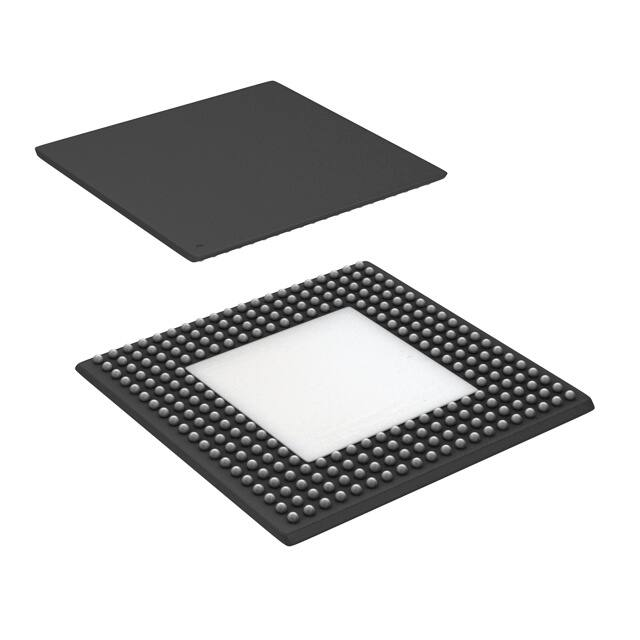


 工商网监
湘ICP备2023018690号
工商网监
湘ICP备2023018690号
