CYRF9935
WirelessUSB™ NX 2.4 GHz
Low Power Radio
Key Features
■
Programmable Multi-Level FIFO
❐ 3 Levels of 32 bytes each
❐ 6 Levels of 16 bytes each
■
RF channel – 126 (2400 MHz~2525 MHz)
■
Programmable Data Rate – 2 Mbps/250 Kbps
■
Automatic Packet Acknowledgement
■
Power Supply Range – 1.9 V to 3.6 V
■
Automatic Packet Resend
■
Ultra low power operation
❐ TX Current 12 mA at 0 dBm output power
❐ RX Current 15 mA at 2 Mbps data rate
❐ RX Current 14 mA at 250 Kbps data rate
❐ Idle current 26 µA (Idle-I mode)
❐ Sleep current 900 nA
■
8/16 bit hardware CRC
■
Up to 8 Pipes for 1:8 Star Network
■
4-pin Hardware SPI Interface
■
±60 ppm 16 MHz crystal
■
Compact 24-pin 4 × 4 mm QFN package
■
■
Programmable TX Output Power:
❐ +4 dBm
❐ 0 dBm
❐ –8 dBm
❐ –14 dBm
❐ –20 dBm
Applications
Sensitivity (0.1%BER):
❐ –93 dBm at 250 kbps
❐ –82 dBm at 2 Mbps
■
Digital RSSI
■
Programmable Payload length – 1 to 32 bytes
■
Wireless mouse, keyboard, gamepad and presenter
■
Wireless audio and VoRF
■
Remote controller
■
Home automation
■
Wireless sensor network
■
Radio Controlled (R/C) Toy
Block Diagram
Transmitter
Baseband
TX FIFO
SPI_nSS
SCK
MISO
GFSK
Modulator
X
PA
SPI
Baseband
Engine
(Framer)
MOSI
IRQ
MODE
ANT2
Receiver
Register
Map
GFSK
Demodulator
X
LNA
RX FIFO
•
198 Champion Court
Frequency
Synthesizer
XIN
XOUT
VIN
VDD_PA
VDD_LDO
GND
Power
Management
Cypress Semiconductor Corporation
Document Number: 001-88748 Rev. *G
ANT1
•
San Jose, CA 95134-1709
•
408-943-2600
Revised May 9, 2017
Not recommended for new designs
WirelessUSB™ NX 2.4 GHz Low Power Radio
�CYRF9935
General Description ......................................................... 3
Pin Configuration ............................................................. 3
Pin Descriptions ............................................................... 4
Functional Overview ........................................................ 5
Power on Reset ........................................................... 5
External Reset ............................................................. 5
Interrupt ....................................................................... 5
RF Pins ........................................................................ 5
RF Channel ................................................................. 5
Transmit Power control ............................................... 6
RSSI Operation ........................................................... 7
Power Management .......................................................... 8
Idle-I Mode .................................................................. 9
Sleep Mode ................................................................. 9
Transmit Mode .......................................................... 10
Receive Mode ........................................................... 10
Idle II Mode ................................................................ 10
Baseband Engine ........................................................... 10
Packet Format ........................................................... 10
Preamble ................................................................... 10
Address ..................................................................... 11
Packet Control Word ................................................. 13
Broadcast Address .................................................... 13
Auto-Retransmit Mode .............................................. 14
Data Packet Loss ...................................................... 17
ACK Packet Loss ...................................................... 18
FIFO Control .................................................................... 19
Overview ................................................................... 19
TX FIFO Access ........................................................ 19
RX FIFO Access ........................................................ 21
SPI Command ................................................................. 21
SPI Timing ................................................................. 21
Document Number: 001-88748 Rev. *G
Command List ........................................................... 22
SPI Status in Command Phase ................................. 23
SPI Command for Register Read and Write ............. 23
SPI Command for RX FIFO Access .......................... 23
SPI Command for TX FIFO Access .......................... 24
Register Sets ................................................................... 26
Indirect Registers ...................................................... 31
Application Circuit .......................................................... 33
Absolute Maximum Ratings .......................................... 35
Operating Range ............................................................. 35
Electrical Specifications ................................................ 35
Power Consumption .................................................. 35
General RF Conditions .............................................. 36
Transmitter Operation ............................................... 36
Receiver Operation ................................................... 37
Crystal Specification .................................................. 37
DC Characteristics .................................................... 38
Power-On Reset ........................................................ 38
Ordering Information ...................................................... 39
Ordering Code Definitions ......................................... 39
Packaging Information ................................................... 40
Acronyms ........................................................................ 41
Document Conventions ................................................. 41
Units of Measure ....................................................... 41
Document History Page ................................................. 42
Sales, Solutions, and Legal Information ...................... 47
Worldwide Sales and Design Support ....................... 47
Products .................................................................... 47
PSoC® Solutions ...................................................... 47
Cypress Developer Community ................................. 47
Technical Support ..................................................... 47
Page 2 of 47
Not recommended for new designs
Contents
�CYRF9935
General Description
CYRF9935 is a low power radio transceiver operating in the
world wide 2.4–2.5 GHz ISM band. The transceiver contains fully
integrated receiver, transmitter, frequency synthesizer and
baseband engine. Internal voltage regulators ensure good
immunity to power supply noise and wide power supply voltage
range.
CYRF9935 offers a high data rate of 2 Mbps. It enables burst
transmission to reduce the average power consumption. In
addition, the built-in automatic acknowledgement, automatic
re-send and low power consumption in Idle-I mode, are very
useful features for low power wireless applications.
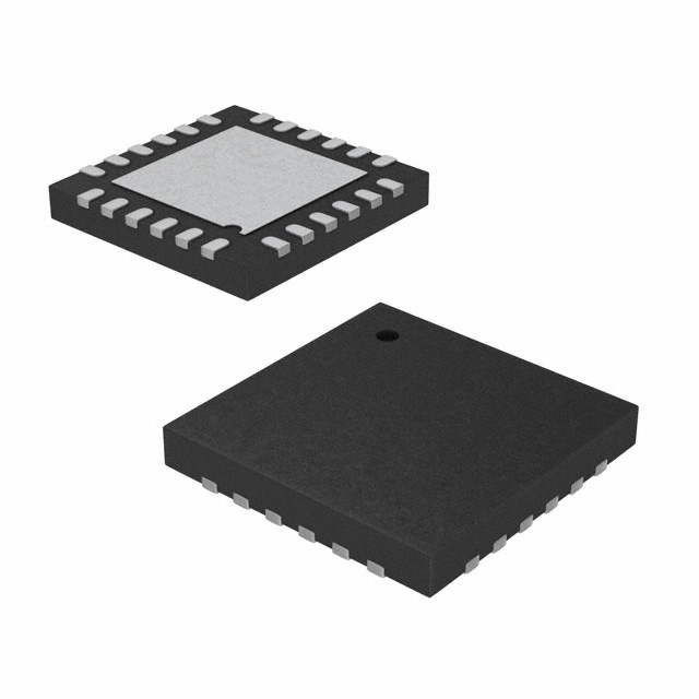
Pin Configuration
Not recommended for new designs
SCK
MOSI
MODE
SPI_nSS
GND
18
17
16
QFN
(Top View) 15
14
13
7
8
9
10
11
12
1
2
3
4
5
6
VIN
GND
GND
ANT2
ANT1
VDD_PA
VIN
XOUT
XIN
GND
GND
VIN
MISO
RST_n
Test1
Test2
VDD_LDO
GND
24
23
22
21
20
19
IRQ
Figure 1. 24-pin QFN Pinout (Top View)
Document Number: 001-88748 Rev. *G
Page 3 of 47
�CYRF9935
Pin Descriptions
Name
Function
Description
SPI data output
[1]
1
MISO
Digital Output
2
RST_n [2]
Digital Input
3
Test1
--
Reserved for factory test. Do not connect.
4
Test2
--
Reserved for factory test. Do not connect.
5
VDD_LDO
Power Output
Chip reset pin. Active low.
Internal digital supply output (1.8 V) for de-coupling purpose only and cannot be
loaded.
6
GND
Power
7
VIN [3]
Power Input
Ground
8
XOUT
Analog Output
Crystal pin 2
9
XIN
Analog Input
Crystal pin 1
Power supply (+1.9 VDC ~ +3.6 VDC)
10
GND
Power
Ground
11
GND
Power
Ground
12
VIN [3]
Power Input
13
VDD_PA
Analog Output
14
ANT1
RF
15
ANT2
RF
16
GND
Power
17
GND
Power
18
VIN [3]
Power Input
Power supply (+1.9 VDC ~ +3.6 VDC)
Power supply output (+1.8 Vdc) for the internal Power Amplifier, for de-coupling
purpose only and cannot be loaded.
Antenna interface pin 1
Antenna interface pin 2
Ground
Ground
Power supply (+1.9 VDC ~ +3.6 VDC)
19
GND
Power
20
SPI_nSS
Digital Input
Ground
21
MODE
Digital Input
Chip enable activates RX mode. Active high.
22
MOSI
Digital Input
SPI data input
23
SCK
Digital Input
24
IRQ
Digital Output
SPI chip select. Active low.
SPI clock input
Interrupt pin. Active low (default). Can be programmed to active high by
setting internal register (address: 0x02).
Notes
1. MISO pin on the PSoC must be configured in pull-up mode to achieve low current consumption in Idle-I and Sleep modes. If using any other controller an external
pull-up may be required.
2. RST_n line has an internal pull-up resistor which will pulls it high, hence the user does not need to pull RST_n high.
3. Pins 7, 12 and 18 i.e. all VIN pins must be shorted to a common power supply.
Document Number: 001-88748 Rev. *G
Page 4 of 47
Not recommended for new designs
Pin
�CYRF9935
Functional Overview
the radio for about 1.5 milliseconds. This is required for the
crystal oscillator to start-up.
Power on Reset
External reset is an atomic command (it cannot be interrupted)
and will interrupt any other activity on the chip.
External Reset
CYRF9935 can also be reset anytime by driving the RST_n pin
low for a period greater than 5 µs. The reset signal should be
followed by a period of inactivity on the SPI or any other input to
Interrupt
In CYRF9935 the interrupt is provided through the IRQ pin. The
interrupt can be configured as active low or active high, by
clearing or setting bit 7 of direct register 0x02 respectively. Upon
reset, it is configured as active low.
There are six interrupt sources in CYRF9935. These interrupts
can be enabled or disabled by configuring bits 5:0 of direct
register 0x02 (refer to Register Sets on page 26). Table 1
describes the different interrupts that are available.
Table 1. Interrupt Sources
Interrupt source
Description
RX_DR
TX_DS
TX_MAX_ARSC
TX_FIFO
RX data ready
TX data sent
Maximum retry reached
Change in TX FIFO state to
the state selected by the
TX_FIFO_STA_SEL bits in
register 0x28
RX FIFO not empty
RSSI refresh done
RX_FIFO
RSSI
Bit in Register 0x02 for enabling or
disabling interrupt
5
4
3
2
Bit in Register 0x01 (Status) that
reflects the state of interrupt
5
4
3
1
1
0
0
2
If an interrupt is enabled the IRQ pin reflects the state of the
corresponding interrupt source in the register 0x01 (refer to
Register Sets on page 26). The IRQ pin remains asserted till the
interrupt is cleared. To clear an interrupt set the corresponding
bit in status register.
CYRF9935
ANT1
ANT2
The CYRF9935 has two RF pins, ANT1 and ANT2, which are
used for differential RF input/output. For optimum performance,
an LC network (called a matching network) matches WUSB-NX
to a conventional 50-ohm antenna.
50 Ohm line
Matching network
The traces to ANT1 and ANT2 pins are RF traces and should be
short and direct.
The LC values of the matching network should not be modified
from those shown in the Application Circuit on page 33. In
addition to matching, they provide attenuation of undesired
transmit harmonics. These components should have good
high-frequency characteristics, signified by Q factor within the
manufacturer datasheets.
On the other side of the matching network is an antenna with
50 Ohm impedance. This trace also should be short, if possible.
However, in many cases, the antenna needs to be placed in a
more optimum position on the PCB, so some additional trace
length may be necessary. In such cases, the characteristic
impedance of trace should also be 50 Ohm.
There should be a solid ground plane on the underside of the
matching network. The solid ground plane should extend all the
Document Number: 001-88748 Rev. *G
RF Pins
Antenna
way to the ground pad vias (at the center of the device) on one
side and should extend to the 50 Ohm transmission line that
connects to the antenna on the other side.
RF Channel
The RF channel frequency determines the center of the channel
used. The channel occupies a bandwidth of less than 1 MHz at
250 kbps and a bandwidth of less than 2 MHz at 2 Mbps.
CYRF9935 can operate on frequencies from 2.400 GHz to 2.525
GHz. The programming resolution of the RF channel frequency
setting is 1MHz.
At 2 Mbps the channel occupies a bandwidth wider than the
resolution of the RF channel frequency setting. To ensure
non-overlapping channels in 2 Mbps mode, the channel spacing
must be 2 MHz or more. At 250 kbps the occupied channel
bandwidth is the same or lower than the resolution of the RF
channel frequency setting.
Page 5 of 47
Not recommended for new designs
Power on reset is initiated when the voltage on VIN reaches
1.9 V. It takes 50 ms for the power on reset event to complete.
After power on reset the radio registers will have default values
(refer to Register Sets on page 26) and the radio will be in Idle-I
mode. In this mode the radio consumes 26 µA current.
�CYRF9935
Table 2. RF channel frequency (continued)
Channel Number (Decimal)
Frequency
2
2402 MHz
3
2403 MHz
4
2404 MHz
5
2405 MHz
Table 2. RF channel frequency
Frequency
…….
…….
0
2400 MHz
125
2525 MHz
1
2401 MHz
Channel Number (Decimal)
Table 3. Registers Table for Channel Setting
Address (Hex)
Name
Bits
Init
RW
0x00
Channel
6:0
0101000
R/W
Transmit Power control
CYRF9935 supports 5 transmit power levels, which are +4 dBm,
0 dBm, –8 dBm, –14 dBm and –20 dBm.The +4 dBm power
output is set using the indirect register 0x04 bit 7 (see Indirect
Registers on page 31 for instructions on using the indirect
Description
RF Channel Number
registers). The other four power levels can be set using the bits
4:3 of direct register 0x03.
The table below summarizes the power levels available.
Table 4. For 4 dbm setting
Indirect Register
Address (Hex)
Mnemonic
Bit
Reset Value
Type
Description
0x04
PA4DBM
7
0
R/W
Enable PA 4 dBm output power.
1: PA output power 4dBm
0: PA output power depends on RF_PWR setting
in direct register 0x03.
Reserved
6:0
0010001
R
Only ‘0010001’ allowed
Table 5. For Other power settings
Address (Hex)
Mnemonic
Bit
Reset Value
Type
0x03
RF_PWR
3:2
00
R/W
Document Number: 001-88748 Rev. *G
Description
RF output power
00: –20 dBm
01: –14 dBm
10: –8 dBm
11: 0 dBm
Page 6 of 47
Not recommended for new designs
The RF channel frequency is set by the register 0x00 according
to the following formula:
Frequency = 2400 + Channel [MHz]
The transmitter and the receiver must be programmed with the
same RF channel frequency to communicate with each other.
�CYRF9935
RSSI Operation
CYRF9935 supports two types of RSSI measurements namely,
RSSI Refresh and Packet RSSI.
RSSI Refresh is used to implement “Channel Assessment”. This
means RSSI Refresh can be used to assess whether a channel
is clean or not. It is useful to search a clean channel for
Frequency Hopping Spread Spectrum implementations. RSSI
Refresh requires the user to specify the RF channel for RSSI
measurement in the Channel field of register 0x00 prior to RSSI
measurements. RSSI Refresh is enabled by setting
AUTO_RSSI_EN or RSSI_REFRESH bit fields of register 0x20.
When AUTO_RSSI_EN is set, CYRF9935 evaluates RSSI
continuously until AUTO_RSSI_EN is cleared. With
RSSI_REFRESH enabled, CYRF9935 evaluates RSSI only
once, after which RSSI_REFRESH will be cleared automatically.
During RSSI evaluation, the RSSI result is updated onto the
RSSI_VAL_MSB and RSSI_VAL_LSB bit fields of register 0x20.
The RSSI value format is shown as below:
MSB
Bit 3
Bit 2
LSB
Bit 1
Bit 0
Bit 6
For example, when you start a RSSI refresh and get the value “0110_0101” from the register 0x20. The real RSSI value is “01011”.
Packet RSSI can be used to estimate the distance between TXer and RXer. CYRF9935 evaluates RSSI after the address field in
packet being received is matched. We can use R_RX_PAYLOAD command to get the Packet RSSI if RSSI_AUTO_EN is set.
Table 7. Registers Table for RSSI Operation
Address (Hex)
Mnemonic
Bits
Init
RW
0x00
Channel
6:0
0101000
R/W
RF channel
0x20
RSSI_VAL_LSB
6
0
R/W
RSSI LSB (Bit 0) Value
This value is updated by RSSI Refresh function
AUTO_RSSI_ EN
5
0
R/W
AUTO RSSI Enable
0: AUTO RSSI Disable
1: AUTO RSSI Enable
RSSI_REFRESH
4
0
R/W
RSSI Refresh
Set to 1 to start RSSI refresh. The bit is auto cleared
when RSSI Refresh is done. RSSI Refresh value will
update in RSSI_VAL_MSB and RSSI_VAL_LSB
RSSI_VAL_MSB
3:0
0
R/W
RSSI MSB (Bit 4–1) Value
This value is updated by RSSI Refresh function
Document Number: 001-88748 Rev. *G
Description
Page 7 of 47
Not recommended for new designs
Table 6. RSSI value format
�CYRF9935
Power Management
CYRF9935 has a built in state machine that controls the transition between the various operating states/modes of the radio. The state
machine takes input from the various register settings, MODE pin and internal signals. The state diagram is shown in the figure below
and conditions under which the state transition happens is explained in the table below.
Figure 2. State Diagram
Power off
Not recommended for new designs
RST_n = 0 from any state
16
Sleep
(~900nA)
1
Reset
3
4
2
Idle I
(~26 uA)
15
5
9
8
11
Idle II
(~700 uA)
RX Settling
很抱歉,暂时无法提供与“CYRF9935-24LQXC”相匹配的价格&库存,您可以联系我们找货
免费人工找货