CYS25G0101DX
SONET OC-48 Transceiver
SONET OC-48 Transceiver
Features
Functional Description
■
SONET OC-48 operation
■
Bellcore and ITU jitter compliance
■
2.488 GBaud serial signaling rate
■
Multiple selectable loopback or loop through modes
The CYS25G0101DX SONET OC-48 Transceiver is a
communications building block for high speed SONET data
communications. It provides complete parallel-to-serial and
serial-to-parallel conversion, clock generation, and clock and
data recovery operations in a single chip optimized for full
SONET compliance.
■
Single 155.52 MHz reference clock
Transmit Path
■
Transmit FIFO for flexible data interface clocking
■
16-bit parallel-to-serial conversion in transmit path
■
Serial-to-16-bit parallel conversion in receive path
■
Synchronous parallel interface
❐ LVPECL compliant
❐ HSTL compliant
New data is accepted at the 16-bit parallel transmit interface at
a rate of 155.52 MHz. This data is passed to a small integrated
FIFO to enable flexible transfer of data between the SONET
processor and the transmit serializer. As each 16-bit word is read
from the transmit FIFO, it is serialized and sent out to the high
speed differential line driver at a rate of 2.488 Gbits per second.
■
Internal transmit and receive phase-locked loops (PLLs)
■
Differential CML serial input
❐ 50 mV input sensitivity
❐ 100internal termination and DC restoration
■
Differential CML serial output
❐ Source matched for 50 transmission lines (100 differential
transmission lines)
Receive Path
■
Direct interface to standard fiber optic modules
■
Less than 1.0W typical power
■
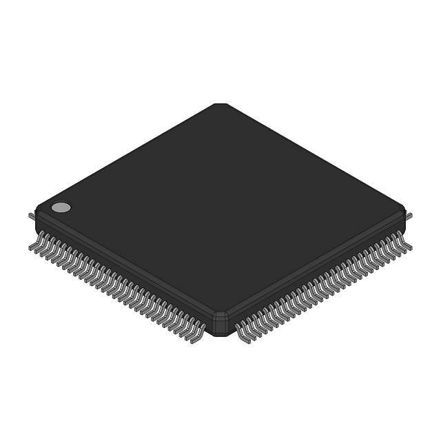
120-pin 14 mm × 14 mm TQFP
■
Standby power saving mode for inactive loops
■
0.25 BiCMOS technology
■
Pb-free packages available
Cypress Semiconductor Corporation
Document Number: 38-02009 Rev. *O
As serial data is received at the differential line receiver, it is
passed to a clock and data recovery (CDR) PLL that extracts a
precision low jitter clock from the transitions in the data stream.
This bit rate clock is used to sample the data stream and receive
the data. Every 16-bit times, a new word is presented at the
receive parallel interface along with a clock.
Parallel Interface
The parallel I/O interface supports high speed bus communications using HSTL signaling levels to minimize both power
consumption and board landscape. The HSTL outputs are
capable of driving unterminated transmission lines of less than
70 mm and terminated 50 transmission lines of more than twice
that length.
The CYS25G0101DX Transceiver’s parallel HSTL I/O can also
be configured to operate at LVPECL signaling levels. This is
done externally by changing VDDQ, VREF and creating a simple
circuit at the termination of the transceiver’s parallel output
interface.
•
198 Champion Court
•
San Jose, CA 95134-1709
•
408-943-2600
Revised October 24, 2013
�CYS25G0101DX
Logic Block Diagram
(155.52 MHz)
TXCLKI TXD[15:0]
FIFO_ERR
TXCLKO
(155.52 MHz)
RXCLK
(155.52 MHz)
REFCLK
RXD[15:0]
FIFO_RST
16
16
Input
Register
Output
Register
FIFO
TX PLL
X16
16
Shifter
16
Recovered
Bit-Clock
TX Bit-Clock
Shifter
RX CDR
PLL
Retimed
Data
Lock-to-Ref
LOOPTIME
DIAGLOOP
Lock-to-Data/
Clock Control
Logic
LINELOOP
LOOPA
OUT
Document Number: 38-02009 Rev. *O
PWRDN LOCKREF
SD
LFI
RESET
IN
Page 2 of 22
�CYS25G0101DX
Contents
Clocking ............................................................................ 4
Pin Configuration ............................................................. 5
Pin Descriptions ............................................................... 6
CYS25G0101DX Operation .............................................. 8
CYS25G0101DX Transmit Data Path ............................... 8
Operating Modes ......................................................... 8
Phase Align Buffer ....................................................... 8
Transmit PLL Clock Multiplier ...................................... 8
Serializer ..................................................................... 8
Serial Output Driver ..................................................... 8
CYS25G0101DX Receive Data Path ................................ 8
Serial Line Receivers .................................................. 8
Lock to Data Control .................................................... 8
Clock Data Recovery ................................................... 8
External Filter .............................................................. 8
Deserializer ................................................................. 9
Loopback Timing Modes ............................................. 9
Reset Modes ............................................................... 9
Power Down Mode ...................................................... 9
LVPECL Compliance ................................................... 9
Maximum Ratings ........................................................... 10
Power Up Requirements ........................................... 10
Operating Range ............................................................. 10
Document Number: 38-02009 Rev. *O
DC Specifications ........................................................... 10
DC Specifications ........................................................... 10
DC Specifications ........................................................... 11
DC Specifications ........................................................... 11
DC Specifications ........................................................... 12
AC Test Loads and Waveforms ..................................... 12
AC Specifications ........................................................... 13
AC Specifications ........................................................... 13
AC Specifications ........................................................... 14
Jitter Specifications ....................................................... 14
Jitter Waveforms ............................................................ 15
Switching Waveforms .................................................... 16
Typical IO Terminations ................................................. 17
Ordering Information ...................................................... 19
Ordering Code Definitions ......................................... 19
Package Diagram ............................................................ 20
Document History Page ................................................. 21
Sales, Solutions, and Legal Information ...................... 22
Worldwide Sales and Design Support ....................... 22
Products .................................................................... 22
PSoC® Solutions ...................................................... 22
Cypress Developer Community ................................. 22
Technical Support ..................................................... 22
Page 3 of 22
�CYS25G0101DX
Clocking
The source clock for the transmit data path is selectable from
either the recovered clock or an external BITS (Building
Integrated Timing Source) reference clock. The low jitter of the
CDR PLL enables loop timed operation of the transmit data path
meeting all Bellcore and ITU jitter requirements.
Multiple loopback and loop through modes are available for both
diagnostic and normal operation. For systems containing
redundant SONET rings that are maintained in standby, the
CYS25G0101DX may also be dynamically powered down to
conserve system power.
System or Telco Bus
Figure 1. CYS25G0101DX System Connections
SONET Data
Processor
16
Transmit Data
Interface
Host Bus
Interface
Document Number: 38-02009 Rev. *O
Receive Data
Interface
16
CYS25G0101DX
TXD[15:0]
TXCLKI
FIFO_RST
FIFO_ERR
TXCLKO
REFCLK
2
155.52 MHz
BITS Time
Reference
RXD[15:0]
RXCLK
Data & Clock
Direction
Control
LOOPTIME
DIAGLOOP
LOOPA
LINELOOP
Status and
System
Control
RESET
PWRDN
LOCKREF
LFI
IN+
IN–
SD
OUT–
OUT+
Serial Data
Serial Data
RD+
RD–
SD
TD–
TD+
Optical
XCVR
Optical
Fiber Links
Page 4 of 22
�CYS25G0101DX
Pin Configuration
VCCQ
VSSQ
VCCQ
NC
NC
VSSQ
NC
VSSQ
VCCQ
NC
NC
102
101
100
99
98
96
95
94
93
92
NC
O U T+
103
91
O U T–
104
97
CM_SER
107
VCCQ
VSSQ
108
105
IN–
109
106
VCCQ
IN+
110
VCCQ
VSSQ
111
VSSQ \NC*
113
112
RXCN1
114
115
RXCN2
VCCQ \NC*
RXCP1
116
118
117
VSSQ \NC*
RXCP2
119
NC
VCCQ
VSSQ
REFCLK+
REFCLK–
NC
LOOPTIME
PW RDN
VSSN
VCCN
VSSN
TXCLKO
VSSN
VDDQ
TXD[0]
TXD[1]
TXD[2]
TXD[3]
VCCQ
VSSQ
VCCN
VSSN
TXD[4]
TXD[5]
TXD[6]
TXD[7]
TXD[8]
TXD[9]
TXD[10]
TXD[11]
VREF
VCC N
VSSN
TXCLKI
TXD[12]
TXD[13]
TXD[14]
TXD[15]
FIFO_RST
FIFO_ERR
VSSN
VCC N
VSSN
VDDQ
RXD[15]
RXD[14]
RXD[13]
RXD[12]
VD DQ
RXD[10]
RXD[11]
RXD[9]
VC CQ
RXD[8]
NC
74
73
72
71
70
69
68
67
66
65
64
63
62
61
32 33 34 35 36 37 38 39 40 41 42 43 44 45 46 47 48 49 50 51 52 53 54 55 56 57 58 59 60
VSSN
NC
25
26
27
28
29
30
31
VSSQ
NC
17
18
19
20
21
22
23
24
90
89
88
87
86
85
84
83
82
81
80
79
78
77
76
75
CYS25G0101DX
VCCQ
NC
VSSN
SD
LOCKREF
RXD[0]
RXD[1]
RXD[2]
RXD[3]
VSSN
VDDQ
RXD[4]
RXD[5]
RXD[6]
RXD[7]
VSSN
VDDQ
R XCLK
VSSN
VDDQ
NC
NC
NC
Top View
1
2
3
4
5
6
7
8
9
10
11
12
13
14
15
16
VSSQ
LFI
RESET
DIAGLOOP
LINELOOP
LOOPA
VSSN
VCCN
VSSN
120
Figure 2. 120-pin TQFP pinout [1, 2]
Notes
1. No connect (NC) pins are left unconnected or floating. Connecting any of these pins to the positive or negative power supply causes improper operation or failure of
the device.
2. Pins 113 and 119 are either no connect or VSSQ. Use VSSQ for compatibility with next generation of OC-48 SERDES devices. Pin 116 are either no connect or VCCQ.
Use VCCQ for compatibility with next generation of OC-48 SERDES devices.
Document Number: 38-02009 Rev. *O
Page 5 of 22
�CYS25G0101DX
Pin Descriptions
CYS25G0101DX OC-48 SONET Transceiver
Pin Name
I/O Characteristics
Signal Description
Transmit Path Signals
TXD[15:0]
HSTL inputs,
sampled by TXCLKI
Parallel Transmit Data Inputs. A 16-bit word, sampled by TXCLKI. TXD[15] is the most
significant bit (the first bit transmitted).
TXCLKI
HSTL Clock input
Parallel Transmit Data Input Clock. The TXCLKI is used to transfer the data into the input
register of the serializer. The TXCLKI samples the data, TXD [15:0], on the rising edge of
the clock cycle.
TXCLKO
HSTL Clock output
Transmit Clock Output. Divide by 16 of the selected transmit bit rate clock. It is used to
coordinate byte wide transfers between upstream logic and the CYS25G0101DX.
VREF
Input Analog Reference Reference Voltage for HSTL Parallel Input Bus. VDDQ/2.[3]
Receive Path Signals
RXD[15:0]
HSTL output,
synchronous
Parallel Receive Data Output. These outputs change following RXCLK. RXD[15] is the
most significant bit of the output word and is received first on the serial interface.
RXCLK
HSTL Clock output
Receive Clock Output. Divide by 16 of the bit rate clock extracted from the received serial
stream. RXD [15:0] is clocked out on the falling edge of the RXCLK.
CM_SER
Analog
Common Mode Termination. Capacitor shunt to VSS for common mode noise.
RXCN1
Analog
Receive Loop Filter Capacitor (Negative).
RXCN2
Analog
Receive Loop Filter Capacitor (Negative).
RXCP1
Analog
Receive Loop Filter Capacitor (Positive).
RXCP
Analog
Receive Loop Filter Capacitor (Positive).
Device Control and Status Signals
REFCLK±
Differential LVPECL
input
Reference Clock. This clock input is used as the timing reference for the transmit and
receive PLLs. A derivative of this input clock is used to clock the transmit parallel interface.
The reference clock is internally biased enabling for an AC coupled clock signal.
LFI
LVTTL output
Line Fault Indicator. When LOW, this signal indicates that the selected receive data stream
is detected as invalid by either a LOW input on SD or by the receive VCO operated outside
its specified limits.
RESET
LVTTL input
Reset for all logic functions except the transmit FIFO.
LOCKREF
LVTTL input
Receive PLL Lock to Reference. When LOW, the receive PLL locks to REFCLK instead
of the received serial data stream.
SD
LVTTL input
Signal Detect. When LOW, the receive PLL locks to REFCLK instead of the received serial
data stream. The SD needs to be connected to an external optical module to indicate a loss
of received optical power.
FIFO_ERR
LVTTL output
Transmit FIFO Error. When HIGH, the transmit FIFO has either underflowed or overflowed.
When this occurs, the FIFO’s internal clearing mechanism clears the FIFO within nine clock
cycles. In addition, FIFO_RST is activated at device power up to ensure that the in and out
pointers of the FIFO are set to maximum separation.
FIFO_RST
LVTTL input
Transmit FIFO Reset. When LOW, the in and out pointers of the transmit FIFO are set to
maximum separation. FIFO_RST is activated at device power up to ensure that the in and
out pointers of the FIFO are set to maximum separation. When the FIFO is reset, the output
data is a 1010... pattern.
PWRDN
LVTTL input
Device Power Down. When LOW, the logic and drivers are all disabled and placed into a
standby condition where only minimal power is dissipated.
Note
3. VREF equals to (VCC – 1.33V) if interfacing to a parallel LVPECL interface.
Document Number: 38-02009 Rev. *O
Page 6 of 22
�CYS25G0101DX
Pin Descriptions (continued)
CYS25G0101DX OC-48 SONET Transceiver
Pin Name
I/O Characteristics
Signal Description
Loop Control Signals
DIAGLOOP
LVTTL input
Diagnostic Loopback Control. When HIGH, transmit data is routed through the receive
clock and data recovery. It is then presented at the RXD[15:0] outputs. When LOW, received
serial data is routed through the receive clock and data recovery. It is then presented at the
RXD[15:0] outputs.
LINELOOP
LVTTL input
Line Loopback Control. When HIGH, received serial data is looped back from receive to
transmit after being reclocked by a recovered clock. When LINELOOP is LOW, the data
passed to the OUT± line driver is controlled by LOOPA. When both LINELOOP and LOOPA
are LOW, the data passed to the OUT± line driver is generated in the transmit shifter.
LOOPA
LVTTL input
Analog Line Loopback. When LINELOOP is LOW and LOOPA is HIGH, received serial
data is looped back from receive input buffer to transmit output buffer but is not routed
through the clock and data recovery PLL. When LOOPA is LOW, the data passed to the
OUT± line driver is controlled by LINELOOP.
LOOPTIME
LVTTL input
Loop Time Mode. When HIGH, the extracted receive bit clock replaces transmit bit clock.
When LOW, the REFCLK input is multiplied by 16 to generate the transmit bit clock.
OUT±
Differential CML
output
Differential Serial Data Output. This differential CML output (+3.3 V referenced) is capable
of driving terminated 50 transmission lines or commercial fiber optic transmitter modules.
IN±
Differential CML
input
Differential Serial Data Input. This differential input accepts the serial data stream for
deserialization and clock extraction.
VCCN
Power
+3.3 V supply (for digital and low speed IO functions)
VSSN
Ground
Signal and power ground (for digital and low speed IO functions)
VCCQ
Power
+3.3 V quiet power (for analog functions)
VSSQ
Ground
Quiet ground (for analog functions)
VDDQ
Power
+1.5 V supply for HSTL outputs[4]
Serial I/O
Power
Note
4. VDDQ equals VCC if interfacing to a parallel LVPECL interface.
Document Number: 38-02009 Rev. *O
Page 7 of 22
�CYS25G0101DX
CYS25G0101DX Operation
CYS25G0101DX Receive Data Path
The CYS25G0101DX is a highly configurable device designed
to support reliable transfer of large quantities of data using high
speed serial links. It performs necessary clock and data
recovery, clock generation, serial-to-parallel conversion, and
parallel-to-serial conversion. CYS25G0101DX also provides
various loopback functions.
Serial Line Receivers
CYS25G0101DX Transmit Data Path
Operating Modes
The transmit path of the CYS25G0101DX supports 16-bit wide
data paths.
Phase Align Buffer
Data from the input register is passed to a phase align buffer
(FIFO). This buffer is used to absorb clock phase differences
between the transmit input clock and the internal character clock.
Initialization of the phase align buffer takes place when the
FIFO_RST input is asserted LOW. When FIFO_RST is returned
HIGH, the present input clock phase, relative to TXCLKO, is set.
Once set, the input clock is enabled to skew in time up to half a
character period in either direction relative to REFCLK (that is,
±180. This time shift enables the delay path of the character
clock (relative to REFLCK) to change due to operating voltage
and temperature not affecting the desired operation. FIFO_RST
is an asynchronous input. FIFO_ERR is the transmit FIFO Error
indicator. When HIGH, the transmit FIFO has either underflowed
or overflowed. The FIFO is externally reset to clear the error
indication; or if no action is taken, the internal clearing
mechanism clears the FIFO in nine clock cycles. When the FIFO
is being reset, the output data is 1010.
Transmit PLL Clock Multiplier
The Transmit PLL Clock Multiplier accepts a 155.52 MHz
external clock at the REFCLK input. It multiplies that clock by 16
to generate a bit rate clock for use by the transmit shifter. The
operating serial signaling rate and allowable range of REFCLK
frequencies is listed in Table on page 13. The REFCLK phase
noise limits to meet SONET compliancy are shown in Figure 8
on page 15. The REFCLK± input is a standard LVPECL input.
Serializer
The parallel data from the phase align buffer is passed to the
Serializer that converts the parallel data to serial data. It uses the
bit rate clock generated by the Transmit PLL clock multiplier.
TXD[15] is the most significant bit of the output word and is
transmitted first on the serial interface.
Serial Output Driver
The Serial Interface Output Driver makes use of high
performance differential Current Mode Logic (CML) to provide a
source matched driver for the transmission lines. This driver
receives its data from the Transmit Shifters or the receive
loopback data. The outputs have signal swings equivalent to that
of standard LVPECL drivers and are capable of driving AC
coupled optical modules or transmission lines.
Document Number: 38-02009 Rev. *O
A differential line receiver, IN±, is available for accepting the input
serial data stream. The serial line receiver inputs accommodate
high wire interconnect and filtering losses or transmission line
attenuation (VSE > 25 mV, or 50 mV peak-to-peak differential). It
can be AC coupled to +3.3V or +5V powered fiber optic interface
modules. The common mode tolerance of these line receivers
accommodates a wide range of signal termination voltages.
Lock to Data Control
Line Receiver routed to the clock and data recovery PLL is
monitored for:
■ status of signal detect (SD) pin
■ status of LOCKREF pin.
This status is presented on the Line Fault Indicator (LFI) output,
that changes asynchronously in the cases in which SD or
LOCKREF go from HIGH to LOW. Otherwise, it changes
synchronously to the REFCLK.
Clock Data Recovery
The extraction of a bit rate clock and recovery of data bits from
received serial stream is performed by a Clock Data Recovery
(CDR) block. The clock extraction function is performed by high
performance embedded phase-locked loop (PLL) that tracks the
frequency of the incoming bit stream and aligns the phase of the
internal bit rate clock to the transitions in the selected serial data
stream.
CDR accepts a character rate (bit rate * 16) reference clock on
the REFCLK input. This REFCLK input is used to ensure that the
VCO (within the CDR) is operating at the correct frequency
(rather than some harmonic of the bit rate), to improve PLL
acquisition time and to limit unlocked frequency excursions of the
CDR VCO when no data is present at the serial inputs.
Regardless of the type of signal present, the CDR attempts to
recover a data stream from it. If the frequency of the recovered
data stream is outside the limits set by the range controls, the
CDR PLL tracks REFCLK instead of the data stream. When the
frequency of the selected data stream returns to a valid
frequency, the CDR PLL is allowed to track the received data
stream. The frequency of REFCLK must be within ±100 ppm of
the frequency of the clock that drives the REFCLK signal of the
remote transmitter to ensure a lock to the incoming data stream.
For systems using multiple or redundant connections, the LFI
output can be used to select an alternate data stream. When an
LFI indication is detected, external logic toggles selection of the
input device. When such a port switch takes place, it is
necessary for the PLL to reacquire lock to the new serial stream.
External Filter
The CDR circuit uses external capacitors for the PLL filter. A
0.1 F capacitor needs to be connected between RXCN1 and
RXCP1. Similarly a 0.1 F capacitor needs to be connected
between RXCN2 and RXCP2. The recommended packages and
dielectric material for these capacitors are 0805 X7R or 0603
X7R.
Page 8 of 22
�CYS25G0101DX
Deserializer
The CDR circuit extracts bits from the serial data stream and
clocks these bits into the Deserializer at the bit clock rate. The
Deserializer converts serial data into parallel data. RXD[15] is the
most significant bit of the output word and is received first on the
serial interface.
Loopback Timing Modes
CYS25G0101DX supports various
described in the following sections.
loopback
modes,
as
Facility Loopback (Line Loopback with Retiming)
When the LINELOOP signal is set HIGH, the Facility Loopback
mode is activated and the high speed serial receive data (IN±) is
presented to the high speed transmit output (OUT±) after
retiming. In Facility Loopback mode, the high speed receive data
(IN±) is also converted to parallel data and presented to the low
speed receive data output pins (RXD[15:0]). The receive
recovered clock is also divided down and presented to the low
speed clock output (RXCLK).
Equipment Loopback (Diagnostic Loopback with Retiming)
When the DIAGLOOP signal is set HIGH, transmit data is looped
back to the RX PLL, replacing IN±. Data is looped back from the
parallel TX inputs to the parallel RX outputs. The data is looped
back at the internal serial interface and goes through transmit
shifter and the receive CDR. SD is ignored in this mode.
Line Loopback Mode (Non-retimed Data)
When the LOOPA signal is set HIGH, the RX serial data is
directly buffered out to the transmit serial data. The data at the
serial output is not retimed.
Document Number: 38-02009 Rev. *O
Loop Timing Mode
When the LOOPTIME signal is set HIGH, the TX PLL is
bypassed and the receive bit rate clock is used for the transmit
side shifter.
Reset Modes
ALL logic circuits in the device are reset using RESET and
FIFO_RST signals. When RESET is set LOW, all logic circuits
except FIFO are internally reset. When FIFO_RST is set LOW,
the FIFO logic is reset.
Power Down Mode
CYS25G0101DX provides a global power down signal PWRDN.
When LOW, this signal powers down the entire device to a
minimal power dissipation state. RESET and FIFO_RST signals
should be asserted LOW along with PWRDN signal to ensure
low power dissipation.
LVPECL Compliance
The CYS25G0101DX HSTL parallel I/O can be configured to
LVPECL compliance with slight termination modifications. On
the transmit side of the transceiver, the TXD[15:0] and TXCLKI
are made LVPECL compliant by setting VREF (reference voltage
of a LVPECL signal) to VCC – 1.33 V. To emulate an LVPECL
signal on the receiver side, set the VDDQ to 3.3 V and the
transmission lines needs to be terminated with the Thévenin
equivalent of Z at LVPECL ref. The signal is then attenuated
using a series resistor at the driver end of the line to reduce the
3.3 V swing level to a LVPECL swing level (see Figure 14 on
page 17). This circuit needs to be used on all 16 RXD[15:0] pins,
TXCLKO, and RXCLK. The voltage divider is calculated
assuming the system is built with 50 transmission lines.
Page 9 of 22
�CYS25G0101DX
Maximum Ratings
Latch up Current .................................................... > 200 mA
Exceeding maximum ratings may shorten the useful life of the
device. User guidelines are not tested.
Power Up Requirements
Storage Temperature ............................... –65 °C to +150 °C
Ambient Temperature with
Power Applied ......................................... –55 °C to +125 °C
VCC Supply Voltage to Ground Potential .....–0.5 V to +4.2 V
VDDQ Supply Voltage to Ground Potential ...–0.5 V to +4.2 V
DC Voltage Applied to HSTL Outputs
in High Z State .................................. –0.5 V to VDDQ + 0.5 V
DC Voltage Applied to Other Outputs
in High Z State .................................... –0.5 V to VCC + 0.5 V
Power supply sequencing is not required if you are configuring
VDDQ = 3.3 V and all power supplies pins are connected to the
same 3.3 V power supply.
Power supply sequencing is required if you are configuring
VDDQ = 1.5 V. Power is applied in the following sequence: VCC
(3.3) followed by VDDQ (1.5). Power supply ramping may occur
simultaneously as long as the VCC/VDDQ relationship is
maintained.
Operating Range
Range
Ambient
Temperature
DC Input Voltage ................................ –0.5 V to VCC + 0.5 V
Commercial
0 °C to +70 °C
Static Discharge Voltage
(MIL-STD-883, Method 3015) ................................. > 1100 V
Industrial
Output Current into LVTTL Outputs (LOW) ................ 30 mA
VDDQ
VCC
1.4 V to 1.6 V [5] 3.3 V ± 10%
–40 °C to +85 °C 1.4 V to 1.6 V [5] 3.3 V ± 10%
DC Specifications
LVTTL
Parameter
Description
Test Conditions
Min
Max
Unit
2.4
–
V
–
0.4
V
–20
–90
mA
LVTTL Outputs
VOHT
Output HIGH Voltage
VCC = Min, IOH = –10.0 mA
VOLT
Output LOW Voltage
VCC = Min, IOL = 10.0 mA
IOS
Output Short Circuit Current
VOUT = 0 V
LVTTL Inputs
VIHT
Input HIGH Voltage
Low = 2.1 V, High = VCC + 0.5 V
2.1
VCC – 0.3
V
VILT
Input LOW Voltage
Low = –3.0 V, High = 0.8
–0.3
0.8
V
IIHT
Input HIGH Current
VCC = Max, VIN = VCC
–
50
A
IILT
Input LOW Current
VCC = Max, VIN = 0 V
–
–50
A
Input Capacitance
VCC = Max, at f = 1 MHz
–
5
pF
Typ
Max
Unit
300
347
mA
–
5
mA
Capacitance
CIN
DC Specifications
Power
Parameter
Description
Test Conditions
Power
ICC1
Active Power Supply Current
ISB
Standby Current
Note
5. VDDQ equals VCC if interfacing to a parallel LVPECL interface.
Document Number: 38-02009 Rev. *O
Page 10 of 22
�CYS25G0101DX
DC Specifications
Differential LVPECL Compatible Inputs (REFCLK) [6]
Min
Max
Unit
VINSGLE
Parameter
Input Single-ended Swing
Description
Test Conditions
200
600
mV
VDIFFE
Input Differential Voltage
400
1200
mV
VIEHH
Highest Input HIGH Voltage
VCC – 1.2
VCC – 0.3
V
VIELL
Lowest Input LOW Voltage
IIEH
Input HIGH Current
VIN = VIEHH Max.
–
750
A
IIEL
Input LOW Current
VIN = VIELL Min.
–200
–
A
–
4
pF
Min
Max
Unit
VCC – 2.0 VCC – 1.45
V
Capacitance
CINE
Input Capacitance
DC Specifications
Differential CML [6]
Parameter
Description
Test Conditions
Transmitter CML compatible Outputs
VOHC
Output HIGH Voltage
(VCC Referenced)
100 differential load
VCC – 0.5 VCC – 0.15
V
VOLC
Output LOW Voltage
(VCC Referenced)
100 differential load
VCC – 1.2
VCC – 0.7
V
VDIFFOC
Output Differential Swing
100 differential load
560
1600
mV
VSGLCO
Output Single-ended Voltage
100 differential load
280
800
mV
Receiver CML compatible Inputs
VINSGLC
Input Single-ended Swing
25
1000
mV
VDIFFC
Input Differential Voltage
50
2000
mV
VICHH
Highest Input HIGH Voltage
–
VCC
V
VICLL
Lowest Input LOW Voltage
1.2
–
V
Figure 3. Differential Waveform Definition
V(+)
VSGL
V(-)
VD
0.0V
VDIFF=V(+)-V(-)
Note
6. See Figure 3 for differential waveform definition.
Document Number: 38-02009 Rev. *O
Page 11 of 22
�CYS25G0101DX
DC Specifications
HSTL
Parameter
Description
Test Conditions
Min
Max
Unit
HSTL Outputs
VOHH
Output HIGH Voltage
VCC = min, IOH= –4.0 mA
VDDQ – 0.4
V
VOLH
Output LOW Voltage
VCC = min, IOL= 4.0 mA
0.4
V
IOSH
Output Short Circuit Current
VOUT = 0V
100
mA
HSTL Inputs
VIHH
Input HIGH Voltage
VREF + 0.13 VDDQ + 0.3
–0.3
VREF – 0.1
V
VILH
Input LOW Voltage
IIHH
Input HIGH Current
VDDQ = max, VIN = VDDQ
50
A
IILH
Input LOW Current
VDDQ = max, VIN = 0V
–40
A
Input Capacitance
VDDQ = max, at f = 1 MHz
5
pF
V
Capacitance
CINH
AC Test Loads and Waveforms
Figure 4. AC Waveforms
VICHH
3.0V
3.0V
Vth = 1.4V
GND
2.0V
2.0V
0.8V
0.8V
80%
Vth = 1.4V
< 1 ns
< 1 ns
20%
VICLL
< 150 ps
(a) LVTTL Input Test Waveform
VIEHH
80%
80%
80%
Vth = 0.75V
20%
20%
< 150 ps
(b) CML Input Test Waveform
VIHH
Vth = 0.75V
80%
20%
VIHL
< 1 ns
< 1 ns
80%
20%
20%
VIELL
< 1.0 ns
< 1.0 ns
(d) LVPECL Input Test Waveform
(c) HSTL Input Test Waveform
Figure 5. AC Test Loads
1.5V
3.3V
R1
OUTPUT
R1 = 330
R2 = 510
CL 10 pF
(Includes fixture and
probe capacitance)
OUT+
CL
(a) TTL AC Test Load
Document Number: 38-02009 Rev. *O
RL = 100
R2
OUT–
RL
(b) CML AC Test Load
R1
OUTPUT
R1 = 100
R2 = 100
CL 7 pF
(Includes fixture and
probe capacitance)
CL
R2
(c) HSTL AC Test Load
Page 12 of 22
�CYS25G0101DX
AC Specifications
Parallel Interface
Parameter
Description
Min
Max
Unit
tTS
TXCLKI Frequency (must be frequency coherent to REFCLK)
154.5
156.5
MHz
tTXCLKI
TXCLKI Period
6.38
6.47
ns
tTXCLKID
TXCLKI Duty Cycle
40
60
%
tTXCLKIR
TXCLKi Rise Time
0.3
1.5
ns
tTXCLKIF
TXCLKi Fall Time
0.3
1.5
ns
tTXDS
Write Data Setup toof TXCLKI
1.5
–
ns
tTXDH
Write Data Hold fromof TXCLKI
0.5
–
ns
tTOS
TXCLKO Frequency
154.5
156.5
MHz
tTXCLKO
TXCLKO Period
6.38
6.47
ns
tTXCLKOD
TXCLKO Duty Cycle
43
57
%
tTXCLKOR
TXCLKO Rise Time
0.3
1.5
ns
tTXCLKOF
TXCLKO Fall Time
0.3
1.5
ns
tRS
RXCLK Frequency
154.5
156.5
MHz
tRXCLK
RXCLK Period
6.38
6.47
ns
tRXCLKD
RXCLK Duty Cycle
43
57
%
0.3
1.5
ns
0.3
1.5
ns
tRXCLKR
RXCLK Rise
tRXCLKF
RXCLK Fall
tRXDS
Time[7]
Time[7]
Recovered Data Setup with reference to of RXCLK
2.2
–
ns
tRXDH
Recovered Data Hold with reference to of RXCLK
2.2
–
ns
tRXPD
Valid Propagation Delay
–1.0
1.0
ns
AC Specifications
REFCLK [8]
Min
Max
Unit
tREF
Parameter
REFCLK Input Frequency
Description
154.5
156.5
MHz
tREFP
REFCLK Period
6.38
6.47
ns
tREFD
REFCLK Duty Cycle
35
65
%
data)[9]
tREFT
REFCLK Frequency Tolerance — (relative to received serial
–100
+100
ppm
tREFR
REFCLK Rise Time
0.3
1.5
ns
tREFF
REFCLK Fall Time
0.3
1.5
ns
Notes
7. RXCLk rise time and fall times are measured at the 20 to 80 percentile region of the rising and falling edge of the clock signal.
8. The 155.52 MHz Reference Clock Phase Noise Limits for the CYS25G0101DX are shown in Figure 8.
9. +20 ppm is required to meet the SONET output frequency specification.
Document Number: 38-02009 Rev. *O
Page 13 of 22
�CYS25G0101DX
AC Specifications
CML Serial Outputs
Parameter
Description
Min
Typ
Max
Unit
tRISE
CML Output Rise Time (20–80%, 100 balanced load)
60
–
170
ps
tFALL
CML Output Fall Time (80–20%, 100 balanced load)
60
–
170
ps
Min
Typ [10]
Max [10]
Unit
–
0.03
0.04
UI
Jitter Specifications
Parameter
tTJ-TXPLL
tTJ-RXPLL
Description
Total Output Jitter for TX PLL (p-p)
[11]
Total Output Jitter for TX PLL (rms)
[11, 12]
–
0.007
0.008
UI
Total Output Jitter for RX CDR PLL (p-p)
[11]
–
0.035
0.05
UI
Total Output Jitter for RX CDR PLL (rms)
[11, 12]
–
0.008
0.01
UI
Notes
10. Typical values are measured at room temperature and the Max values are measured at 0 °C.
11. The RMS and P-to-P jitter values are measured using a 12 KHz to 20 MHz SONET filter.
12. This device passes the Bellcore specification from -10 °C to 85 °C.
Document Number: 38-02009 Rev. *O
Page 14 of 22
�CYS25G0101DX
Jitter Waveforms
Figure 6. Jitter Transfer Waveform of CYS25G0101DX [13]
Figure 7. Jitter Tolerance Waveform of CYS25G0101DX [13]
Figure 8. CYS25G0101DX Reference Clock Phase Noise Limits
Notes
13. The bench jitter measurements are performed using an Agilent Omni bert SONET jitter tester.
Document Number: 38-02009 Rev. *O
Page 15 of 22
�CYS25G0101DX
Switching Waveforms
Figure 9. Transmit Interface Timing
tTXCLKI
tTXCLKIDH
tTXCLKIDL
TXCLKI
t TXDS tTXDH
TXD[15:0]
tTXCLKO
tTXCLKODL
tTXCLKODH
TXCLKO
Figure 10. Receive Interface Timing
tRXCLK
tRXCLKDL
tRXCLKDH
RXCLK
t RXPD
t RXDS
tRXDH
RXD[15:0]
Document Number: 38-02009 Rev. *O
Page 16 of 22
�CYS25G0101DX
Typical IO Terminations
Figure 11. Serial Input Termination
CY S25G0101DX
Limiting Amp
0.1 F
Zo=50
IN+
OUT+
100
OUT–
IN–
Zo=50
0.1 F
Figure 12. Serial Output termination [14]
Optical Module
CY S25G0101DX
0.1 F
Zo=50
IN+
OUT+
100
OUT–
IN–
Zo=50
0.1 F
Figure 13. TXCLKO/ RXCLK Termination
FRAMER
CY S25G0101DX
VDDQ=1.5V
Zo=50
HSTL
OUTPU
T
100
HSTL
INPUT
100
Figure 14. RXD[15:0] Termination
CY S25G0101DX
FRAMER
Zo=50
HSTL
OUTPU
T
HSTL
INPUT
Figure 15. LVPECL Compliant Output Termination
VDDQ=3.3V
RXD[15; 0],
RXCLK,
TXCLKO OUTPUT
FRAMER
VDDQ=3.3V
137
Zo=50
80.6
LVPECL INPUT
121
CY S25G0101DX
Note
14. Serial output of CYS25G0101DX is source matched to 50 transmission lines (100 differential transmission lines).
Document Number: 38-02009 Rev. *O
Page 17 of 22
�CYS25G0101DX
Typical IO Terminations (continued)
Figure 16. AC Coupled Clock Oscillator Termination
Clock Oscillator
Zo=50
LVPEC L
OUTPUT
130
82
Zo=50
CY S25G0101DX
VCC
VCC
0.1uF
VCC
130
82
Refcloc k Inter nall y
Biased
0.1uF
Figure 17. Clock Oscillator Termination
Clock Oscillator
Zo=50
LVPEC L
OUTPUT
Document Number: 38-02009 Rev. *O
130
82
Zo=50
CY S25G0101DX
VCC
VCC
130
82
Reference Cloc k Input
Page 18 of 22
�CYS25G0101DX
Ordering Information
Speed
Standard
Ordering Code
CYS25G0101DX-AEXC
Package
Name
AE120
Package Type
120-pin TQFP (Pb-free)
Operating
Range
Commercial
Ordering Code Definitions
CY S 25G
01
01 DX - AE X C
Temperature Range: C = Commercial
Pb-free
Package Type: AE = 120-pin TQFP
Integrated Tx/Rx Channel
Parallel 16 I/O Bus
Single Channel
2.5 Gbps Support
Technology Code: S = SONET
Company ID: CY = Cypress
Document Number: 38-02009 Rev. *O
Page 19 of 22
�CYS25G0101DX
Package Diagram
Figure 18. 120-pin TQFP (14 × 14 × 1.0 mm) AE120A (6.5 × 6.5 E-Pad) Package Outline, 001-48723
001-48723 *B
Document Number: 38-02009 Rev. *O
Page 20 of 22
�CYS25G0101DX
Document History Page
Document Title: CYS25G0101DX SONET OC-48 Transceiver
Document Number: 38-02009
Rev.
ECN No.
Submission
Date
Orig. of
Change
**
105847
03/22/01
SZV
Change from Specification number: 38-00894 to 38-02009.
*A
108024
06/20/01
AMV
Changed Marketing part number.
*B
111834
12/18/01
CGX
Updated power specification in features and DC specifications section.
Changed pinout for compatibility with CYS25G0102DX in pin diagram and
descriptions. Verbiage added or changed for clarity in pin descriptions section.
Changed input sensitivity in Receive Data Path section, page 6. RXCLK rise
time corrected to 0.3 nSec min CML and LVPECL input waveforms updated in
test load and waveform section. Diagrams replaced for clarity Figures 1-10.
Added two Refclock diagrams Figures 9 and 10.
*C
112712
02/06/02
TME
Updated temperature range, static discharge voltage, and max total RMS jitter.
*D
113791
04/24/02
CGX
Updated the single ended swing and differential swing voltage for Receiver
CML compatible inputs. Created a separate table showing peak to peak and
RMS jitter for both TX PLL and RX PLL.
*E
115940
05/22/02
TME
Added Industrial temperature specification to pages 8, 11, and 15.
*F
117906
09/06/02
CGX
Added differential waveform definition.
Added BGA pinout and package information.
Changed LVTTL VIHT min from 2.0 to 2.1 volts.
*G
119267
10/17/02
CGX
Added phase noise limits data.
Removed BGA pinout and package information.
Removed references to CYS25G0102DX.
*H
121019
11/06/02
CGX
Removed “Preliminary” from datasheet
Description of Change
*I
122319
12/30/02
RBI
Added power up requirements to Maximum Ratings information
*J
124438
02/13/03
WAI
Revised power up requirements
*K
1309983
07/27/07
*L
2647349
01/26/09
AAE /
PYRS
Revised the ordering information to only reflect the new marketing part
numbers defined for the new 120AE (e-pad) package.
Updated the package diagram per spec 001-48723.
*M
2897889
03/23/10
CGX
Removed inactive parts from Ordering Information.
Updated Package Diagram.
IUS / SFV Added Pb-free logo
Added Pb-free parts to the Ordering Information:
CYS25G0101DX-ATXC, CYS25G0101DX-ATXI
*N
3051122
10/07/10
NVNS
Added Ordering Code Definitions.
*O
4173317
10/24/2013
NVNS
Updated Package Diagram:
spec 001-48723 – Changed revision from *A to *B.
Updated in new template.
Completing Sunset Review.
Document Number: 38-02009 Rev. *O
Page 21 of 22
�CYS25G0101DX
Sales, Solutions, and Legal Information
Worldwide Sales and Design Support
Cypress maintains a worldwide network of offices, solution centers, manufacturer’s representatives, and distributors. To find the office
closest to you, visit us at Cypress Locations.
PSoC® Solutions
Products
Automotive
Clocks & Buffers
Interface
Lighting & Power Control
cypress.com/go/automotive
cypress.com/go/clocks
cypress.com/go/interface
cypress.com/go/powerpsoc
psoc.cypress.com/solutions
PSoC 1 | PSoC 3 | PSoC 4 | PSoC 5LP
Cypress Developer Community
Community | Forums | Blogs | Video | Training
cypress.com/go/plc
Memory
cypress.com/go/memory
PSoC
cypress.com/go/psoc
Touch Sensing
cypress.com/go/support
cypress.com/go/touch
USB Controllers
Wireless/RF
Technical Support
cypress.com/go/USB
cypress.com/go/wireless
© Cypress Semiconductor Corporation, 2001-2013. The information contained herein is subject to change without notice. Cypress Semiconductor Corporation assumes no responsibility for the use of
any circuitry other than circuitry embodied in a Cypress product. Nor does it convey or imply any license under patent or other rights. Cypress products are not warranted nor intended to be used for
medical, life support, life saving, critical control or safety applications, unless pursuant to an express written agreement with Cypress. Furthermore, Cypress does not authorize its products for use as
critical components in life-support systems where a malfunction or failure may reasonably be expected to result in significant injury to the user. The inclusion of Cypress products in life-support systems
application implies that the manufacturer assumes all risk of such use and in doing so indemnifies Cypress against all charges.
Any Source Code (software and/or firmware) is owned by Cypress Semiconductor Corporation (Cypress) and is protected by and subject to worldwide patent protection (United States and foreign),
United States copyright laws and international treaty provisions. Cypress hereby grants to licensee a personal, non-exclusive, non-transferable license to copy, use, modify, create derivative works of,
and compile the Cypress Source Code and derivative works for the sole purpose of creating custom software and or firmware in support of licensee product to be used only in conjunction with a Cypress
integrated circuit as specified in the applicable agreement. Any reproduction, modification, translation, compilation, or representation of this Source Code except as specified above is prohibited without
the express written permission of Cypress.
Disclaimer: CYPRESS MAKES NO WARRANTY OF ANY KIND, EXPRESS OR IMPLIED, WITH REGARD TO THIS MATERIAL, INCLUDING, BUT NOT LIMITED TO, THE IMPLIED WARRANTIES
OF MERCHANTABILITY AND FITNESS FOR A PARTICULAR PURPOSE. Cypress reserves the right to make changes without further notice to the materials described herein. Cypress does not
assume any liability arising out of the application or use of any product or circuit described herein. Cypress does not authorize its products for use as critical components in life-support systems where
a malfunction or failure may reasonably be expected to result in significant injury to the user. The inclusion of Cypress’ product in a life-support systems application implies that the manufacturer
assumes all risk of such use and in doing so indemnifies Cypress against all charges.
Use may be limited by and subject to the applicable Cypress software license agreement.
Document Number: 38-02009 Rev. *O
Revised October 24, 2013
All products and company names mentioned in this document may be the trademarks of their respective holders.
Page 22 of 22
�