Please note that Cypress is an Infineon Technologies Company.
The document following this cover page is marked as “Cypress” document as this is the
company that originally developed the product. Please note that Infineon will continue
to offer the product to new and existing customers as part of the Infineon product
portfolio.
Continuity of document content
The fact that Infineon offers the following product as part of the Infineon product
portfolio does not lead to any changes to this document. Future revisions will occur
when appropriate, and any changes will be set out on the document history page.
Continuity of ordering part numbers
Infineon continues to support existing part numbers. Please continue to use the
ordering part numbers listed in the datasheet for ordering.
www.infineon.com
�CYW89071
Single-Chip Automotive Grade Bluetooth
Transceiver and Baseband Processor
The Cypress CYW89071 is a monolithic, single-chip, Bluetooth 4.1 compliant, stand-alone baseband processor with an integrated
2.4 GHz transceiver. Manufactured using the industry's most advanced 65 nm CMOS low-power process, the CYW89071 employs
the highest level of integration, eliminating all critical external components, and thereby minimizing the device’s footprint and costs
associated with the implementation of Bluetooth solutions.
The CYW89071 brings current mobile connectivity technology to automotive radio applications and offers automotive Grade 3 (–40°C
to +85°C ambient operating temperature range) performance. The CYW89071 is tested to Automotive Electronics Council (AEC)
guidelines (AEC-Q100) for environmental stress testing and is manufactured in ISO9001 approved and TS16949 certified facilities.
Cypress Part Numbering Scheme
Cypress is converting the acquired IoT part numbers from Broadcom to the Cypress part numbering scheme. Due to this conversion,
there is no change in form, fit, or function as a result of offering the device with Cypress part number marking. The table provides
Cypress ordering part number that matches an existing IoT part number.
Table 1. Mapping Table for Part Number between Broadcom and Cypress
Broadcom Part Number
Cypress Part Number
BCM89071
CYW89071
BCM89071A1CUBXG
CYW89071A1CUBXG
Acronyms and Abbreviations
In most cases, acronyms and abbreviations are defined on first use.
For a comprehensive list of acronyms and other terms used in Cypress documents, go to http://www.cypress.com/glossary.
Applications
■
Bluetooth 4.1 + EDR compliant
■
Class 1 capable with built-in PA
■
Programmable output power control meets Class 1, Class 2,
or Class 3 requirements
■
Uses supply voltages up to 5.5V
■
■
Supports Broadcom SmartAudio® AEC-Q100 environmental
stress guidelines, wide-band speech, subband coding (SBC)
codec, and packet loss concealment (PLC).
■
Automatic frequency detection for standard crystal and TCXO
values when an external 32.768 kHz reference clock is
provided.
■
Ultra-low power consumption
■
Available in 42-bump WLBGA
■
ARM7TDMI-S™–based microprocessor with integrated ROM
and RAM
■
Supports patch RAM download without external memory
■
Automotive data communication
Fractional-N synthesizer supports frequency references from
12 MHz to 52 MHz
Features
■
Automotive hands-free radios
Cypress Semiconductor Corporation
Document Number: 002-14857 Rev. *H
•
198 Champion Court
•
San Jose, CA 95134-1709
•
408-943-2600
Revised April 25, 2017
�CYW89071
Figure 1. System Block Diagram
PCM
CYW89071
UART
GPIO
Memory
SPI
High-Speed
Peripheral Transport
Unit (PTU)
Radio Transceiver
Microprocessor and
Memory Unit (uPU)
Bluetooth Baseband
Core (BBC)
I2S
TCXO
LPO
IoT Resources
Cypress provides a wealth of data at http://www.cypress.com/internet-things-iot to help you to select the right IoT device for your
design, and quickly and effectively integrate the device into your design. Cypress provides customer access to a wide range of
information, including technical documentation, schematic diagrams, product bill of materials, PCB layout information, and software
updates. Customers can acquire technical documentation and software from the Cypress Support Community website
(http://community.cypress.com/).
Document Number: 002-14857 Rev. *H
Page 2 of 51
�CYW89071
Contents
1. Overview ........................................................................ 4
1.1 Major Features ...................................................... 4
1.2 Block Diagram ....................................................... 6
1.3 Automotive Usage Model ...................................... 7
2. Integrated Radio Transceiver ...................................... 8
2.1 Transmitter Path .................................................... 8
2.2 Receiver Path ........................................................ 8
2.3 Local Oscillator Generation ................................... 8
2.4 Calibration ............................................................. 8
2.5 Internal LDO .......................................................... 9
3. Bluetooth Baseband Core ......................................... 10
3.1 Transmit and Receive Functions ......................... 10
3.2 Bluetooth 4.1 + EDR Features ............................ 10
3.3 Frequency Hopping Generator ............................ 10
3.4 Link Control Layer ............................................... 11
3.5 Test Mode Support .............................................. 11
3.6 Power Management Unit ..................................... 11
3.7 Adaptive Frequency Hopping .............................. 13
3.8 Collaborative Coexistence ................................... 13
3.9 Serial Enhanced Coexistence Interface .............. 13
4. Microprocessor Unit ................................................... 15
4.1 NVRAM Configuration Data and Storage ............ 15
4.2 EEPROM ............................................................. 15
4.3 External Reset ..................................................... 15
4.4 One-Time Programmable Memory ...................... 16
5. Peripheral Transport Unit .......................................... 17
Document Number: 002-14857 Rev. *H
5.1 PCM Interface ..................................................... 17
5.2 HCI Transport Detection Configuration ............... 19
5.3 UART Interface .................................................... 19
5.4 SPI ....................................................................... 20
6. Frequency References ............................................... 21
6.1 Crystal Interface and Clock Generation .............. 21
6.2 Crystal Oscillator ................................................. 22
6.3 External Frequency Reference ............................ 22
6.4 Frequency Selection ............................................ 23
6.5 Frequency Trimming ........................................... 23
6.6 LPO Clock Interface ............................................ 24
7. Pin and Signal Descriptions ...................................... 25
7.1 Pin Descriptions .................................................. 25
8. Ball Grid Arrays .......................................................... 27
9. Electrical Characteristics ........................................... 28
9.1 Electrostatic Discharge Specifications ................ 30
9.2 RF Specifications ................................................ 33
9.3 Timing and AC Characteristics ............................ 36
9.4 I2S Interface ........................................................ 43
10. Mechanical Information ........................................... 46
10.1 Tape, Reel, and Packing Specification .............. 47
11. Package Thermal Characteristics ........................... 48
11.1 Thermal Characteristics .................................... 48
12. Ordering Information ................................................ 49
13. References ................................................................ 49
Document History .......................................................... 50
Page 3 of 38
�CYW89071
1. Overview
The Cypress CYW89071 complies with the Bluetooth Core Specification, version 4.1 and is designed for use with a standard Host
Controller Interface (HCI) UART. The combination of the Bluetooth Baseband Core (BBC), a Peripheral Transport Unit (PTU), and an
ARM®-based microprocessor with on-chip ROM provides a complete lower layer Bluetooth protocol stack, including the Link Controller
(LC), Link Manager (LM), and HCI.
1.1 Major Features
Core features of the CYW89071 include:
■
Support for Bluetooth 4.1 + EDR, including the following options:
❐ A whitelist size of 25
❐ Enhanced Power Control
❐ HCI Read Encryption Key Size command
■
Full support for Bluetooth 2.1 + EDR additional features:
❐ Secure Simple Pairing (SSP)
❐ Encryption Pause Resume (EPR)
❐ Enhance Inquiry Response (EIR)
❐ Link Supervision Time Out (LSTO)
❐ Sniff SubRating (SSR)
❐ Erroneous Data (ED)
❐ Packet Boundary Flag (PBF)
■
Built-in Low Drop-Out (LDO) regulators (2)
❐ 1.63 to 5.5V input voltage range
❐ 1.8 to 3.3V intermediate programmable output voltage
■
Integrated RF section
❐ Single-ended, 50 RF interface
❐ Built-in TX/RX switch functionality
❐ TX Class 1 output power capability
❐ -88 dBm RX sensitivity basic rate
■
Supports maximum Bluetooth data rates over HCI UART and SPI interfaces
■
Multipoint operation, with up to seven active slaves
❐ Maximum of seven simultaneous active ACL links
❐ Maximum of three simultaneous active SCO and eSCO links, with Scatternet support
■
Scatternet operation, with up to four active piconets (with background scan and support for ScatterMode)
■
High-speed HCI UART transport support
❐ H4 five-wire UART (four signal wires, one ground wire)
❐ H5 three-wire UART (two signal wires, one ground wire)
❐ Maximum UART baud rates of 4 Mbps
❐ Low-power out-of-band BT_WAKE and HOST_WAKE signaling
❐ VSC from host transport to UART
❐ Proprietary compressing scheme (allows more than two simultaneous A2DP packets and up to five devices at a time)
■
Channel Quality-Driven Data Rate (CQDDR) and packet type selection
■
Standard Bluetooth test modes
■
Extended radio and production test mode features
■
Full support for power savings modes:
❐ Bluetooth standard Hold and Sniff
❐ Deep sleep modes and regulator shutdown
Document Number: 002-14857 Rev. *H
Page 4 of 51
�CYW89071
■
Supports Wide-Band Speech (WBS) over PCM and Packet Loss Concealment (PLC) for better audio quality
■
2-, 3-, and 4-wire coexistence
■
Power Amplifier (PA) shutdown for externally controlled coexistence, such as WIMAX
■
Built-in LPO clock or operation using an external LPO clock
■
TCXO input and auto-detection of all standard handset clock frequencies (supports low-power crystal, which can be used during
Power Saving mode with better timing accuracy)
■
OR gate for combining a host clock request with a Bluetooth clock request (operates even when the Bluetooth core logic is powered
off)
■
Larger patch RAM space to support future enhancements
■
Serial flash Interface with native support for devices from several manufacturers
■
One-Time Programmable (OTP) memory
Document Number: 002-14857 Rev. *H
Page 5 of 51
�CYW89071
1.2 Block Diagram
Figure 2 on page 6 shows the interconnect of the major CYW89071 physical blocks and associated external interfaces.
Figure 2. Functional Block Diagram
JTAG
ARM7TDMI‐S
DMA
Scan JTAG
Address Decoder
Bus Arb
Trap & Patch
Flash
I/F
32‐bit AHB
AHB2EBI
External
Bus I/F
AHB2APB
WD Timer
Remap &
Pause
GPIO+Aux
SW
Timers
AHB2MEM
ROM
384 KB
RAM
112 KB
Calibration &
Control
Digital Demod
Bit Sync
Low Power
Scan
Blue RF Registers
Interrupt
Controller
PCM
32‐bit APB
Bluetooth Radio
LCU
UART
Buffer
APU
Debug UART
Blue RF I/F
SPI/EMPSPI
(Spiffy)
BT Clk/
Hopper
I2C_Master
Rx/Tx
Buffer
FIFO 1
COEX
PMU
LPO
POR
SPIM
JTAG Master
Digital
Modulator
RF
PMU Control
I/O
Port Control
OTP
(128 bytes)
AHB2MEM
Digital
I/O
FIFO 2
SECI
PTU
Document Number: 002-14857 Rev. *H
Page 6 of 16
�CYW89071
1.3 Automotive Usage Model
The CYW89071 is designed to provide a direct interface to automotive systems, as shown in Figure 3. The device has flexible PCM
and UART interfaces, enabling it to transparently connect to existing circuits.
The device incorporates a number of unique features to accommodate integration into automotive systems.
■
The PCM interface provides multiple modes of operation to support both master and slave, as well as hybrid interfacing to one or
more external codec devices.
■
The UART interface supports hardware flow control with tight integration to power control sideband signaling to support the lowest
power operation.
■
Few external components are required for integration.
Figure 3. Automotive Usage Model
Voice
Codec
PCM
1.63V to 5.5V SUPPLY
UART
20 or 26 MHz CRYSTAL
OSCILLATOR *
Host
BT_WAKE
HOST_WAKE
LPO Clock
CYW89071
* The external LPO clock is required if
the main clock is not 20 MHz.
LPO_INPUT
Document Number: 002-14857 Rev. *H
Page 7 of 51
�CYW89071
2. Integrated Radio Transceiver
The CYW89071 has an integrated radio transceiver that has been optimized for use in 2.4 GHz Bluetooth wireless systems. It has
been designed to provide low-power, low-cost, robust communications for applications operating in the globally available 2.4 GHz
unlicensed ISM band. The CYW89071 is fully compliant with the Bluetooth Radio Specification and enhanced data rate specification
and meets or exceeds the requirements to provide the highest communication link quality of service.
2.1 Transmitter Path
The CYW89071 features a fully integrated zero IF transmitter. The baseband transmitted data is digitally modulated in the modem
block and up-converted to the 2.4 GHz ISM band in the transmitter path. The transmitter path consists of signal filtering, I/Q upconversion, a high-output power amplifier (PA), and RF filtering.
The CYW89071 also incorporates modulation schemes to support enhanced data rates.
■
P/4-DQPSK for 2 Mbps
■
8-DPSK for 3 Mbps
2.1.1 Digital Modulator
The digital modulator performs the data modulation and filtering required for the GFSK, /4DQPSK, and 8-DPSK signals. The fully
digital modulator minimizes any frequency drift or anomalies in the modulation characteristics of the transmitted signal and is much
more stable than direct VCO modulation schemes.
2.1.2 Power Amplifier
The CYW89071’s integrated PA can be configured for Class 2 operation, transmitting up to +4 dBm. The PA can also be configured
for Class 1 operation, transmitting up +10 dBm at the chip in gFSK mode, when a minimum supply voltage of 2.5V is applied to VDDTF.
Because of the linear nature of the PA, combined with integrated filtering, minimal external filtering is required to meet Bluetooth and
regulatory harmonic and spurious requirements.
Using a highly linearized, temperature compensated design, the PA can transmit +10 dBm for basic rate and +8 dBm for enhanced
data rates (2 to 3 Mbps). A flexible supply voltage range allows the PA to operate from 1.2V to 3.3V. A minimum supply voltage of
2.5V is required at VDDTF to achieve +10 dBm of transmit power.
2.2 Receiver Path
The receiver path uses a low IF scheme to downconvert the received signal for demodulation in the digital demodulator and bit
synchronizer. The receiver path provides a high degree of linearity, an extended dynamic range, and high order on-chip channel
filtering to ensure reliable operation in the noisy 2.4 GHz ISM band. The front-end topology, with built-in out-of-band attenuation,
enables the device to be used in most applications without off-chip filtering. For integrated handset operation where the Bluetooth
function is integrated close to the cellular transmitter, minimal external filtering is required to eliminate the desensitization of the
receiver by the cellular transmit signal.
2.2.1 Digital Demodulator and Bit Synchronizer
The digital demodulator and bit synchronizer uses the low IF received signal to perform an optimal frequency tracking and bit synchronization algorithm.
2.2.2 Receiver Signal Strength Indicator
The CYW89071 radio provides a Receiver Signal Strength Indicator (RSSI) signal to the baseband so that the controller can take part
in a Bluetooth power-controlled link by providing a metric of its own receiver signal strength to determine whether the transmitter
should increase or decrease its output power.
2.3 Local Oscillator Generation
Local Oscillator (LO) generation provides fast frequency hopping (1600 hops/second) across the 79 maximum available channels.
The LO generation subblock employs an architecture for high immunity to LO pulling during PA operation. The device uses fullyintegrated PLL loop filters.
2.4 Calibration
The radio transceiver features an automated calibration scheme that is fully self-contained in the radio. User interaction is not required
during normal operation or during manufacturing to provide the optimal performance. Calibration optimizes the performance of all
major blocks in the radio, including gain and phase characteristics of filters, matching between key components, and key gain blocks.
Calibration, which takes process and temperature variations into account, occurs transparently during the settling time of the hops,
adjusting for temperature variations as the device cools and heats during normal operation.
Document Number: 002-14857 Rev. *H
Page 8 of 51
�CYW89071
2.5 Internal LDO
Two internal Low Drop-Out (LDO) voltage regulators eliminate the need for external voltage regulators and therefore reduce the BOM.
The first LDO is a preregulator (HV LDO). The second LDO (Main LDO) supplies the main power to the CYW89071 (see Figure 2 on
page 6).
The HV LDO has an input voltage range of 2.3V to 5.5V. The input VBAT is ideal for batteries. The VREGHV output is programmable
from 1.8V to 3.3V, in 100 mV steps. The dropout voltage is 200 mV. The HV LDO can supply up to 95 mA, which leaves spare power
for external circuitry such as an RF power amp for higher transmit power. If the HV LDO is not used, to turn off the HV LDO and
minimize current consumption, connect the VBAT input to the VREGHV output. Firmware can then disable the HV LDO, saving the
quiescent current.
The HV LDO default output voltage is 2.9V, allowing this regulator to be used to power external NV memory devices, as well as the
VDDO rail. The firmware can then adjust this output to as low as 1.8V, if desired, to power VDDTF.
The main LDO has a 1.22V output (VREG) and is used to supply main power to the CYW89071 (see Figure 4). The input of this LDO
(VREGHV) has an input voltage range of from 1.63V to 3.63V. The output of the HV LDO is internally connected to the input to the
main LDO. Power can be applied to VREGHV when the HV LDO is not used. The main LDO supplies power to the entire device for
Class 2 operation. The main LDO can drive up to 60 mA, which leaves spare power for external circuitry. The main LDO is bypassed
by not connecting anything to its output (VREG) and driving 1.12V–1.32V directly to VDDC and VDDRF.
REG_EN provides a control signal for the host to control power to the CYW89071. When power is enabled, the CYW89071 will require
complete initialization.
Figure 4. LDO Functional Block Diagram
CYW89071
HV LDO
REG_EN
Document Number: 002-14857 Rev. *H
VBAT
Main LDO
VREGHV
VREG
Page 9 of 51
�CYW89071
3. Bluetooth Baseband Core
The Bluetooth Baseband Core (BBC) implements the time critical functions required for high-performance Bluetooth operation. The
BBC manages buffering, segmentation, and data routing for all connections. It also buffers data that passes through it, handles data
flow control, schedules SCO/ACL Tx/Rx transactions, monitors Bluetooth slot usage, optimally segments and packages data into
baseband packets, manages connection status indicators, and composes and decodes HCI packets. In addition to these functions, it
independently handles HCI event types and HCI command types.
3.1 Transmit and Receive Functions
The following transmit and receive functions are implemented in the BBC hardware to increase the reliability and security of the Tx/
Rx data before sending the data over the air:
In the transmitter:
■
Data framing
■
Forward Error Correction (FEC) generation
■
Header Error Control (HEC) generation
■
Cyclic Redundancy Check (CRC) generation
■
Key generation
■
Data encryption
■
Data whitening
In the receiver:
■
Symbol timing recovery
■
Data deframing
■
FEC
■
HEC
■
CRC
■
Data decryption
■
Data dewhitening
3.2 Bluetooth 4.1 + EDR Features
The CYW89071 supports Bluetooth 4.1 + EDR, including the following options:
■
A whitelist size of 25
■
Enhanced Power Control
■
HCI Read Encryption Key Size command
The CYW89071 provides full support for Bluetooth 2.1 + EDR additional features:
■
Secure Simple Pairing (SSP)
■
Encryption Pause Resume (EPR)
■
Enhance Inquiry Response (EIR)
■
Link Supervision Time Out (LSTO)
■
Sniff SubRating (SSR)
■
Erroneous Data (ED)
■
Packet Boundary Flag (PBF)
3.3 Frequency Hopping Generator
The frequency hopping sequence generator selects the correct hopping channel number, based on the link controller state, Bluetooth
clock, and device address.
Document Number: 002-14857 Rev. *H
Page 10 of 51
�CYW89071
3.4 Link Control Layer
The Link Control layer is part of the Bluetooth link control functions implemented in dedicated logic in the Link Control Unit (LCU).
This layer consists of the Command Controller that takes commands from the software and other controllers that are activated or
configured by the Command Controller to perform the link control tasks.
There are two major states–Standby and Connection. Each task establishes a different state in the Bluetooth Link Controller. In
addition, there are eight substates—Page, Page Scan, Inquiry, Inquiry Scan, Park, Sniff Subrate, and Hold.
3.5 Test Mode Support
The CYW89071 fully supports Bluetooth Test Mode, including the transmitter tests, normal and delayed loopback tests, and the
reduced hopping sequence.
In addition to the standard Bluetooth Test mode, the device supports enhanced testing features to simplify RF debugging and qualification and type approval testing.
These test features include:
■
Fixed frequency carrier wave (unmodulated) transmission
❐ Simplifies some type approval measurements (Japan)
❐ Aids in transmitter performance analysis
■
Fixed frequency constant receiver mode
❐ Directs receiver output to I/O pin
❐ Allows for direct BER measurements using standard RF test equipment
❐ Facilitates spurious emissions testing for receive mode
■
Fixed frequency constant bit stream transmission
❐ Unmodulated, 8-bit fixed pattern, PRBS-9, or PRBS-15
❐ Enables modulated signal measurements with standard RF test equipment
■
Packetized connectionless transmitter test
❐ Hopping or fixed frequency
❐ Multiple packet types supported
❐ Multiple data patterns supported
■
Packetized connectionless receiver test
❐ Fixed frequency
❐ Multiple packet types supported
❐ Multiple data patterns supported
3.6 Power Management Unit
The Power Management Unit (PMU) provides power management features that can be invoked through power management registers
or packet handling in the baseband core. This section contains descriptions of the PMU features.
3.6.1 RF Power Management
The BBC generates power-down control signals for the transmit path, receive path, PLL, and power amplifier to the 2.4 GHz transceiver. The transceiver then processes the power-down functions, accordingly.
Document Number: 002-14857 Rev. *H
Page 11 of 51
�CYW89071
3.6.2 Host Controller Power Management
The host can place the device in a sleep state, in which all nonessential blocks are powered off and all nonessential clocks are
disabled. Power to the digital core is maintained so that the state of the registers and RAM is not lost. In addition, the LPO clock is
applied to the internal sleep controller so that the chip can wake automatically at a specified time or based on signaling from the host.
The goal is to limit the current consumption to a minimum, while maintaining the ability to wake up and resume a connection with
minimal latency.
If a scan or sniff session is enabled while the device is in Sleep mode, the device automatically will wake up for the scan/sniff event,
then go back to sleep when the event is done. In this case, the device uses its internal LPO-based timers to trigger the periodic wake
up. While in Sleep mode, the transports are idle. However, the host can signal the device to wake up at any time. If signaled to wake
up while a scan or sniff session is in progress, the session continues but the device will not sleep between scan/sniff events. Once
Sleep mode is enabled, the wake signaling mechanism can also be thought of as a sleep signaling mechanism, since removing the
wake status will often cause the device to sleep.
In addition to a Bluetooth device wake signaling mechanism, there is a host wake signaling mechanism. This feature provides a way
for the Bluetooth device to wake up a host that is in a reduced power state.
There are two mechanisms for the device and the host to signal wake status to each other:
Bluetooth WAKE (BT_WAKE) and
Host WAKE (and HOST_WAKE) signaling
The BT_WAKE pin (GPIO_0) allows the host to wake the BT device, and
HOST_WAKE (GPIO_1) is an output that allows the BT device to wake the host.
In-band UART signaling
The CTS and RTS signals of the UART interface are used for BT wake (CTS) and
Host wake (RTS) functions in addition to their normal function on the UART
interface. Note that this applies for both H4 and H5 protocols.
When running in SPI mode, the CYW89071 has a mode where it enters Sleep mode when there is no activity on the SPI interface for
a specified (programmable) amount of time. Idle mode is detected when the SPI_CSN is left deasserted. Whether to sleep on an idle
interface and the amount of time to wait before entering Sleep mode can be programed by the host. Once the CYW89071 enters
sleep, the host can wake it by asserting SPI_CSN. If the host decides to sleep, the CYW89071 will wake up the host by asserting
SPI_INT when it has data for it.
Note: Successful operation of the power management handshaking signals requires coordinated support between the device
firmware and the host software.
Table 2. Power Control Pin Summary
Pin
Direction
Description
Bluetooth device wake-up: Signal from the host to the Bluetooth device that the host requires
attention.
BT_WAKE
(GPIO_0)
Host output
BT input
■
Asserted = Bluetooth device must wake up or remain awake.
Deasserted = Bluetooth device may sleep when sleep criteria are met.
The polarity of this signal is software configurable and can be asserted high or low. By default,
BT_WAKE is active-low (if BT-WAKE is low it requires the device to wake up or remain awake).
■
Host wake-up. Signal from the Bluetooth device to the host indicating that Bluetooth device
requires attention.
HOST_WAKE
(GPIO_1)
BT output
Host input
■
Asserted = Host device must wake up or remain awake.
Deasserted = Host device may sleep when sleep criteria are met.
The polarity of this signal is software configurable and can be asserted high or low.
■
Clock request
CLK_REQ
(GPIO_5)
BT output
■
Asserted = External clock reference required
■
Deasserted = External clock reference may be powered down.
Enables the internal preregulator and main regulator outputs. REG_EN is active-high.
REG_EN
BT input
■
1 = Enabled
■
0 = Disabled
Document Number: 002-14857 Rev. *H
Page 12 of 51
�CYW89071
3.6.3 BBC Power Management
The device provides the following low-power operations for the BBC:
■
Physical layer packet handling turns RF on and off dynamically within packet TX and RX.
■
Bluetooth specified low-power connection modes—Sniff, Hold, and Park. While in these low-power connection modes, the device
runs on the Low Power Oscillator and wakes up after a predefined time period.
Backdrive Protection
The CYW89071 provides a backdrive protection feature that allows the device to be turned off while the host and other devices in the
system remain operational. When the device is not needed in the system, VDD_RF and VDDC are shut down and VDDO remains
powered. This allows the device to be effectively off, while keeping the I/O pins powered so that they do not draw extra current from
other devices connected to the I/O.
Note: VDD_RF collectively refers to the VDDTF, VDDPX, and VDDRF RF power supplies.
Note: Never apply voltage to I/O pins if VDDO is not applied.
During the low power shutdown state and as long as VDDO remains applied to the device, all outputs are tristated and all digital and
analog clocks are disabled. Input voltages must remain within the limits defined for normal operation. This is done to either prevent
current draw and back loading on digital signals in the system. It also enables the device to be fully integrated in an embedded device
and take full advantage of the lowest power savings modes. If VDDC is powered up externally (not connected to VREG), VDDC
requires 750 K to ground during low-power shutdown. If VDDC is powered up by VREG, VDDC does not require 750 K to ground
because the internal main LDO has about 750 K to ground when turned off.
Several signals, including the frequency reference input (XTAL_IN) and external LPO input (LPO_IN), are designed to be highimpedance inputs that will not load down the driving signal, even if VDDO power is not applied to the chip. The other signals with back
drive prevention are RST_N, COEX_OUT0, COEX_OUT1, COEX_IN, PCM_SYNC, PCM_CLK, PCM_OUT, PCM_IN, UART_RTS_N,
UART_CTS_N, UART_RXD, UART_TXD, GPIO_0, GPIO_1, GPIO_2, GPIO_4, GPIO_7, and OTP_DIS.
All other IO signals must remain at VSS until VDDO is applied. Failing to do this can result in unreliable startup behavior.
When powered on, using REG_EN is the same as applying power to the CYW89071. The device does not have information about its
state before being powered-down.
3.7 Adaptive Frequency Hopping
The CYW89071 supports host channel classification and dynamic channel classification Adaptive Frequency Hopping (AFH)
schemes, as defined in the Bluetooth specification.
Host channel classification enables the host to set a predefined hopping map for the device to follow.
If dynamic channel classification is enabled, the device gathers link quality statistics on a channel-by-channel basis to facilitate channel
assessment and channel map selection. To provide a more accurate frequency hop map, link quality is determined using both RF and
baseband signal processing.
3.8 Collaborative Coexistence
The CYW89071 provides extensions and collaborative coexistence to the standard Bluetooth AFH for direct communication with
WLAN devices. Collaborative coexistence enables WLAN and Bluetooth to operate simultaneously in a single device. The device
supports industry-standard coexistence signaling, including 802.15.2, and supports Broadcom and third-party WLAN solutions.
Using a multitiered prioritization approach, relative priorities between data types and applications can be set. This approach maximizes
the performance-WLAN data throughput vs. voice quality versus link performance.
A PA shutdown pin is available to allow full external control of the RF output for other types of coexistence, such as WIMAX.
3.9 Serial Enhanced Coexistence Interface
The Serial Enhanced Coexistence Interface (Serial ECI or SECI) is a proprietary Broadcom interface between Broadcom WLAN
devices and Bluetooth devices. It is an optional replacement to the legacy 3- or 4-wire coexistence feature, which is also available.
The following key features are associated with the interface:
■
Enhanced coexistence data can be exchanged over SECI_IN and SECI_OUT.
■
It supports generic UART communication between WLAN and Bluetooth devices.
■
To conserve power, it is disabled when inactive.
■
It supports automatic resynchronizaton upon waking from sleep mode.
■
It supports a baud rate of up to 4 Mbps.
Document Number: 002-14857 Rev. *H
Page 13 of 51
�CYW89071
3.9.1 SECI Advantages
The advantages of the SECI over the legacy 3-wire coexistence interface are:
■
Only two wires are required: SECI_IN and SECI_OUT.
■
Up to 48-bits of coexistence data can be exchanged.
Previous Cypress stand-alone Bluetooth devices such as the CYW2070 supported only a 3-wire or 4-wire coexistence interface.
Previous Cypress WLAN and Bluetooth combination devices such as the CYW4325, CYW4329, and CYW4330 support an internal
parallel enhanced coexistence interface for more efficient WLAN and Bluetooth information exchange. The SECI allows enhanced
coexistence information to be passed to a companion Broadcom WLAN chip through a serial interface using fewer I/O than the 3-wire
coexistence scheme.
The 48-bits of the SECI significantly enhance WLAN and Bluetooth coexistence by sharing such information as frequencies used and
radio usage times. The exact contents of the SECI are Cypress confidential.
3.9.2 SECI I/O
The CYW89071 does not have dedicated SECI_IN or SECI_OUT pins, but the two pin functions can be mapped to the following digital
I/O: the UART, GPIO, SPIM (or BSC), PCM, and COEX pins. Pin function mapping is controlled by the config file that is either stored
in NVRAM or downloaded directly into on-chip RAM from the host.
Document Number: 002-14857 Rev. *H
Page 14 of 51
�CYW89071
4. Microprocessor Unit
The CYW89071 microprocessor unit runs software from the Link Control (LC) layer up to the Host Controller Interface (HCI). The
microprocessor is based on the ARM7TDMIS 32-bit RISC processor with embedded ICE-RT debug and JTAG interface units. The
microprocessor also includes 384 KB of ROM memory for program storage and boot ROM, 112 KB of RAM for data scratch-pad, and
patch RAM code.
The internal boot ROM provides flexibility during power-on reset to enable the same device to be used in various configurations,
including automatic host transport selection from SPI or UART, with or without external NVRAM. At power-up, the lower layer protocol
stack is executed from the internal ROM.
External patches can be applied to the ROM-based firmware to provide flexibility for bug fixes and features additions. These patches
can be downloaded from the host to the device through the SPI or UART transports, or using external NVRAM. The device can also
support the integration of user applications and profiles using an external serial flash memory.
4.1 NVRAM Configuration Data and Storage
4.1.1 Serial Interface
The CYW89071 includes an SPI master controller that can be used to access serial flash memory. The SPI master contains an AHB
slave interface, transmit and receive FIFOs, and the SPI core PHY logic. Data is transferred to and from the module by the system
CPU. DMA operation is not supported.
The CYW89071 supports serial flash vendors Atmel, MXIC, and Numonyx. The most commonly used parts from two of these vendors
are:
■
AT25BCM512B, manufactured by Atmel
■
MX25V512ZUI-20G, manufactured by MXIC
4.2 EEPROM
The CYW89071 includes a Broadcom Serial Control (BSC) master interface. The BSC interface supports low-speed and fast mode
devices and is compatible with I2C slave devices. Multiple I2C master devices and flexible wait state insertion by the master interface
or slave devices are not supported. The CYW89071 provides 400 kHz, full speed clock support.
The BSC interface is programmed by the CPU to generate the following BSC transfer types on the bus:
■
Read-only
■
Write-only
■
Combined read/write
■
Combined write-read
NVRAM may contain configuration information about the customer application, including the following:
■
Fractional-N information
■
BD_ADDR
■
UART baud rate
■
SDP service record
■
File system information used for code, code patches, or data
4.3 External Reset
The CYW89071 has an integrated power-on reset circuit which completely resets all circuits to a known power on state. This action
can also be driven by an external reset signal, which can be used to externally control the device, forcing it into a power-on reset state.
The RST_N signal input is an active-low signal for all versions of the CYW89071. The CYW89071 requires an external pull-up resistor
on the RST_N input. Alternatively, the RST_N input can be connected to REG_EN or driven directly by a host GPIO.
Document Number: 002-14857 Rev. *H
Page 15 of 51
�CYW89071
4.4 One-Time Programmable Memory
The CYW89071 includes a One-Time Programmable (OTP) memory, allowing manufacturing customization and avoiding the need
for an on-board NVRAM.If customization is not required, then the OTP does not need to be programmed. Whether the OTP is
programmed or not, it is disabled after the boot process completes to save power.
The OTP size is 128 bytes.
The OTP is designed to store a minimal amount of information. Aside from OTP data, most user configuration information will be
downloaded into RAM after the CYW89071 boots up and is ready for host transport communication. The OTP contents are limited to:
■
Parameters required prior to downloading user configuration to RAM.
■
Parameters unique to a customer design.
4.4.1 Contents
The following are typical parameters programmed into the OTP memory:
■
BD_ADDR
■
Software license key
■
Output power calibration
■
Frequency trimming
■
Initial status LED drive configuration
The OTP contents also include a static error correction table to improve yield during the programming process as well as forward error
correction codes to eliminate any long-term reliability problems. The OTP contents associated with error correction are not visible by
customers.
4.4.2 Programming
OTP memory programming takes place through a combination of Broadcom software integrated with the manufacturing test software
and code embedded in CYW89071 firmware.
Programming the OTP requires a 3.3V supply. The OTP programming supply comes from the VDDO pin. The OTP power supply can
be as low as 1.8V in order to read the OTP contents. OTP_DIS is brought out to a pin on the WLBGA package. If the OTP_DIS pin
is left floating or externally pulled low, then the OTP will be enabled. if the OTP_DIS pins is externally pulled high, then the OTP will
be disabled.
Document Number: 002-14857 Rev. *H
Page 16 of 51
�CYW89071
5. Peripheral Transport Unit
This section covers the PCM, UART, and SPI peripheral interfaces. The CYW89071 has a 1040 byte transmit and receive FIFO, which
is large enough to hold the entire payload of the largest EDR BT packet (3-DH5).
5.1 PCM Interface
The CYW89071 PCM interface can connect to linear PCM codec devices in master or slave mode. In master mode, the device
generates the PCM_BCLK and PCM_SYNC signals. In slave mode, these signals are provided by another master on the PCM
interface as inputs to the device.
The device supports up to three SCO or eSCO channels through the PCM interface and each channel can be independently mapped
to any available slot in a frame.
The host can adjust the PCM interface configuration using vendor-specific HCI commands or it can be setup in the configuration file.
5.1.1 System Diagram
Figure 5 shows options for connecting the device to a PCM codec device as a master or a slave.
Figure 5. PCM Interface with Linear PCM Codec
PCM Codec
(Master)
PCM_IN
PCM_OUT
PCM_BCLK
PCM_SYNC
CYW89071
(Slave)
PCM Interface Slave Mode
PCM Codec
(Slave)
PCM_IN
PCM_OUT
PCM_BCLK
PCM_SYNC
CYW89071
(Master)
PCM Interface Master Mode
PCM Codec
(Hybrid)
PCM_IN
PCM_OUT
PCM_BCLK
PCM_SYNC
CYW89071
(Hybrid)
PCM Interface Hybrid Mode
Document Number: 002-14857 Rev. *H
Page 17 of 51
�CYW89071
5.1.2 Slot Mapping
The device supports up to three simultaneous, full-duplex SCO or eSCO channels. These channels are time-multiplexed onto the
PCM interface using a time slotting scheme based on the audio sampling rate, as described in Table 3.
Table 3. PCM Interface Time Slotting Scheme
Audio Sample Rate
Time Slotting Scheme
8 kHz
The number of slots depends on the selected interface rate, as follows:
Interface rate
Slot
128
1
256
2
512
4
1024
8
2048
16
16 kHz
The number of slots depends on the selected interface rate, as follows:
Interface rate
Slot
256
1
512
2
1024
4
2048
8
Transmit and receive PCM data from an SCO channel is always mapped to the same slot. The PCM data output driver tristates its
output on unused slots to allow other devices to share the same PCM interface signals. The data output driver tristates its output after
the falling edge of the PCM clock during the last bit of the slot.
5.1.3 Wideband Speech
The CYW89071 provides support for Wideband Speech (WBS) in two ways:
■
Transparent mode: The host encodes WBS packets and the encoded packets are transferred over the PCM bus for SCO or eSCO
voice connections. In Transparent mode, the PCM bus is typically configured in master mode for a 4 kHz sync rate with 16-bit
samples, resulting in a 64 kbps bit rate.
■
On-chip SmartAudio technology: The CYW89071 can perform SBC encoding and decoding of linear 16 bits at 16 kHz (256 kbps
rate) transferred over the PCM bus.
5.1.4 Frame Synchronization
The device supports both short and long frame synchronization types in both master and slave configurations. In short frame synchronization mode, the frame synchronization signal is an active-high pulse at the 8 kHz audio frame rate (which is a single bit period in
width) and synchronized to the rising edge of the bit clock. The PCM slave expects PCM_SYNC to be high on the falling edge of the
bit clock and the first bit of the first slot to start at the next rising edge of the clock. In the long frame synchronization mode, the frame
synchronization signal is an active-high pulse at the 8 kHz audio frame rate. However, the duration is 3-bit periods and the pulse starts
coincident with the first bit of the first slot.
5.1.5 Data Formatting
The device can be configured to generate and accept several different data formats. The device uses 13 of the 16 bits in each PCM
frame. The location and order of these 13 bits is configurable to support various data formats on the PCM interface. The remaining
three bits are ignored on the input, and may be filled with zeros, ones, a sign bit, or a programmed value on the output. The default
format is 13-bit two’s complement data, left justified, and clocked most significant bit first.
Document Number: 002-14857 Rev. *H
Page 18 of 51
�CYW89071
5.2 HCI Transport Detection Configuration
The CYW89071 supports the following interface types for the HCI transport from the host:
■
UART (H4 and H5)
■
SPI
Only one host interface can be active at a time. The firmware performs a transport detect function at boot-time to determine which
host is the active transport. It can auto-detect the UART interface, but the SPI interface must be selected by strapping the SCL pin to 0.
The complete algorithm is summarized as follows:
1. Determine if SCL is pulled low. If it is, select SPI as HCI host transport.
2. Determine if any local NVRAM contains a valid configuration file. If it does and a transport configuration entry is present, select the
active transport according to entry, and then exit the transport detection routine.
3. Search for CTS_N = 0 on the UART interface. If it is present, select UART.
4. Repeat Step 3 until transport is determined.
5.3 UART Interface
The UART physical interface is a standard, 4-wire interface (RX, TX, RTS, CTS) with adjustable baud rates from 9600 bps to 4.0
Mbps. The interface features an automatic baud rate detection capability that returns a baud rate selection. Alternatively, the baud
rate can be selected via a vendor-specific UART HCI command. The interface supports Bluetooth UART HCI (H4) specifications. The
default baud rate for H4 is 115.2 Kbaud.
The following baud rates are supported:
■
9600
■
14400
■
19200
■
28800
■
38400
■
57600
■
115200
■
230400
■
460800
■
921600
■
1444444
■
1500000
■
2000000
■
3000000
■
3250000
■
3692000
■
4000000
Normally, the UART baud rate is set by a configuration record downloaded after reset or by automatic baud rate detection. The host
does not need to adjust the baud rate. Support for changing the baud rate during normal HCI UART operation is provided through a
vendor-specific command.
The CYW89071 UART operates with the host UART correctly, provided the combined baud rate error of the two devices is within ±2%.
5.3.1 HCI 3-Wire Transport (UART H5)
The CYW89071 supports H5 UART transport for serial UART communications. H5 reduces the number of signal lines required by
eliminating CTS and RTS, when compared to H4. In addition, in-band sleep signaling is supported over the same interface so that
the 4-wire UART and the 2-wire sleep signaling interface can be reduced to a 2-wire UART interface, saving four IOs on the host.
H5 requires the use of an external LPO. CTS must be pulled low.
Document Number: 002-14857 Rev. *H
Page 19 of 51
�CYW89071
5.4 SPI
The CYW89071 supports a slave SPI HCI transport with an input clock range of up to 16 MHz. Higher clock rates may be possible.
The physical interface between the SPI master and the CYW89071 consists of the four SPI signals (SPI_CSB, SPI_CLK, SPI_SI, and
SPI_SO) and one interrupt signal (SPI_INT). The CYW89071 can be configured to accept active-low or active-high polarity on the
SPI_CSB chip select signal. It can also be configured to drive an active-low or active-high SPI_INT interrupt signal. Bit ordering on
the SPI_SI and SPI_SO data lines can be configured as either little-endian or big-endian. Additionally, proprietary sleep mode, halfduplex handshaking is implemented between the SPI master and the CYW89071.
SPI_INT is required to negotiate the start of a transaction. The SPI interface does not require flow control in the middle of a payload.
The FIFO is large enough to handle the largest packet size. Only the SPI master can stop the flow of bytes on the data lines, since it
controls SPI_CSB and SPI_CLK. Flow control should be implemented in higher layer protocols.
Document Number: 002-14857 Rev. *H
Page 20 of 51
�CYW89071
6. Frequency References
The CYW89071 uses two different frequency references for normal and low-power operational modes. An external crystal or
frequency reference driven by a Temperature Compensated Crystal Oscillator (TCXO) signal is used to generate the radio frequencies
and normal operation clocking. Either an external 32.768 kHz or fully integrated internal Low-Power Oscillator (LPO) is used for lowpower mode timing.
6.1 Crystal Interface and Clock Generation
The CYW89071 uses a fractional-N synthesizer to generate the radio frequencies, clocks, and data/packet timing, enabling it to
operate from any of a multitude of frequency sources. The source can be external, such as a TCXO, or a crystal interfaced directly to
the device. The default frequency reference setting is for a 20 MHz crystal or TCXO. The signal characteristics for the crystal interface
are listed in Table 4.
Table 4. Crystal Interface Signal Characteristics
Parameter
Crystal
External Frequency Reference
a
Acceptable frequencies
12–52 MHz in 2 ppm steps
Crystal load capacitance
12 (typical)
12–52 MHz in 2
ppma
Units
steps
–
N/A
pF
ESR
60 (max)
–
Power dissipation
200 (max)
–
W
Input signal amplitude
N/A
400 to 2000
2000 to 3300 (requires a 10 pF DC blocking
capacitor to attenuate the signal)
mVp-p
Signal type
N/A
Square-wave or sine-wave
–
Input impedance
N/A
1
2
M
pF
Phase noise
@ 1 kHz
@ 10 kHz
@ 100 kHz
@ 1 MHz
N/A
N/A
N/A
N/A
N/A
–
< –120b
< –131b
< –136b
< –136b
–
dBc/Hz
dBc/Hz
dBc/Hz
dBc/Hz
12, 13, 14.4, 15.36, 16.2, 16.8, 18, 19.2, 19.44,
19.68, 19.8, 20, 24, 26, 33.6, 37.4, and 38.4
MHz
Auto-detection frequencies when 12, 13, 14.4, 15.36, 16.2, 16.8, 18,
using external LPOc
19.2, 19.44, 19.68, 19.8, 20, 24,
26, 33.6, 37.4, and 38.4
Tolerance without frequency
trimmingd
±20
±20
ppm
Initial frequency tolerance
trimming range
±50
±50
ppm
a. The frequency step size is approximately 80 Hz resolution.
b. With a 26 MHz reference clock. For a 13 MHz clock, subtract 6 dB. For a 52 MHz clock, add 6 dB.
c. Auto-detection of the frequency requires the crystal or external frequency reference to have less than ±50 ppm of variation and also requires an external LPO frequency
which has less than ±250 ppm of variation at the time of detection.
d. AT-Cut crystal or TXCO recommended.
Document Number: 002-14857 Rev. *H
Page 21 of 51
�CYW89071
6.2 Crystal Oscillator
The CYW89071 can use an external crystal to provide a frequency reference. The recommended configuration for the crystal oscillator,
including all external components, is shown in Figure 6.
Figure 6. Recommended Oscillator Configuration
XIN
0 to 18 pF*
Crystal
Oscillator
XOUT
0 to 18 pF*
*Capacitor value range depends
on the manufacturer of the XTAL
as well as board layout.
6.3 External Frequency Reference
An external frequency reference generated by a TCXO signal may be directly connected to the crystal input pin on the CYW89071,
as shown in Figure 7. The external frequency reference input is designed to not change loading on the TCXO when the CYW89071
is powered up or powered down.
When using the CYW89071 with the TXCO OR gate option, GPIO 6 must be driven active high or active low. Excessive leakage
current results if GPIO6 is allowed to float.
Figure 7. Recommended TCXO Connection
TCXO
XIN
10–1000 pF*
No Connection
XOUT
* Recommended value is 100 pF.
Higher values produce a longer startup time.
Lower values have greater isolation.
Larger values help small signal swings.
6.3.1 TCXO Clock Request Support
If the application utilizes an external TCXO as a clock reference, the CYW89071 provides a clock request output to allow the system
to power off the TCXO when not in use. The CYW89071 supports a TCXO OR function that allows a clock request in the system to
be combined with the CYW89071 clock request output, without requiring an extra component on the board.
Clock Request Output
The CLK_REQ signal on the GPIO_5 lead is asserted whenever the CYW89071 is in the Awake state. It is deasserted when in Sleep
state. When the CYW89071 is sleeping, it uses an LPO clock (external or internal) as the timing reference. In the CYW89071, the
clock request output (CLK_REQ) is configured as active high. If the clock request feature is not desired, GPIO_5 can be configured
for other functions.
Document Number: 002-14857 Rev. *H
Page 22 of 51
�CYW89071
TCXO OR Option
The CYW89071 has an optional feature that allows the application to perform a logical OR function on a system TCXO clock request
signal and the CYW89071 clock request to form one clock request output to the TCXO device. This logical OR function is embedded
in the pad ring so that it is available at any time, as long as the pad ring is receiving a VDDO supply. The function works even if the
CYW89071’s digital core is sleeping or completely powered off.
Table 5 shows the truth table.
Table 5. Truth Table
GPIO_6
CLK_REQ_IN
Internal Clock Request State
(0 = sleep)
GPIO_5
CLK_REQ
0
0
0
0
1
1
1
0
1
1
1
1
6.4 Frequency Selection
Any frequency within the range specified for the crystal and TCXO reference can be used. These frequencies include standard handset
reference frequencies (12, 13, 14.4, 15.36, 16.2, 16.8, 18, 19.2, 19.44, 19.68, 19.8, 20, 24, 26, 33.6, 37.4, and 38.4 MHz) and any
frequency between these reference frequencies, as desired by the system designer. Since bit timing is derived from the reference
frequency, the CYW89071 must have the reference frequency set correctly in order for the UART and PCM interfaces to function
properly.
The CYW89071 reference frequency can be set in one of three ways.
■
Use the default 20 MHz frequency
■
Designate the reference frequency in external NVRAM
■
Auto-detect the standard handset reference frequencies using an external LPO clock
The CYW89071 is set to a default frequency of 20 MHz at the factory. For a typical design using a crystal, it is recommended that the
default frequency be used, since this simplifies the design by removing the need for either external NVRAM or external LPO clock.
If the application requires a frequency other than the default, the value can be stored in an external NVRAM. Programming the
reference frequency in NVRAM provides the maximum flexibility in the selection of the reference frequency, since any frequency within
the specified range for crystal and external frequency reference can be used. During power-on reset (POR), the device downloads
the parameter settings stored in NVRAM, which can be programmed to include the reference frequency and frequency trim values.
Typically, this is how a PC Bluetooth application is configured.
For applications such as handsets and portable smart communication devices, where the reference frequency is one of the standard
frequencies commonly used, the CYW89071 automatically detects the reference frequency and programs itself to the correct
reference frequency. In order for auto-frequency detection to work properly, the CYW89071 must have a valid and stable 32.768 kHz
external LPO clock present during POR. This eliminates the need for NVRAM in applications where the external LPO clock is available
and an external NVRAM is typically not used.
6.5 Frequency Trimming
The CYW89071 uses a fractional-N synthesizer to digitally fine-tune the frequency reference input to within ±2 ppm tuning accuracy.
This trimming function can be applied to either the crystal or an external frequency source such as a TCXO. Unlike the typical crystaltrimming methods used, the CYW89071 changes the frequency using a fully digital implementation and is much more stable and
unaffected by crystal characteristics or temperature. Input impedance and loading characteristics remain unchanged on the TCXO or
crystal during the trimming process and are unaffected by process and temperature variations.
The option to use or not use frequency trimming is based on the system designer’s cost trade-off between bill-of-materials (BOM) cost
of the crystal and the added manufacturing cost associated with frequency trimming. The frequency trimming value can either be
stored in the host and written to the CYW89071 as a vendor-specific HCI command or stored in NVRAM and subsequently recalled
during POR.
Frequency trimming is not a substitute for the poor use of tuning capacitors at an crystal oscillator (XTAL). Occasionally, trimming can
help alleviate hardware changes.
Document Number: 002-14857 Rev. *H
Page 23 of 51
�CYW89071
6.6 LPO Clock Interface
The LPO clock is the second frequency reference that the CYW89071 uses to provide low-power mode timing for park, hold, and sniff.
The LPO clock can be provided to the device externally, from a 32.768 kHz source or the CYW89071 can operate using the internal
LPO clock.
The LPO can be internally driven from the main clock. However, sleep current will be impacted.
The accuracy of the internal LPO limits the maximum park, hold, and sniff intervals.
Table 6. External LPO Signal Requirements
Parameter
Nominal input frequency
Frequency accuracy
Input signal amplitude
Signal type
Input impedance (when power is applied or power is off)
Document Number: 002-14857 Rev. *H
External LPO Clock
Units
32.768
kHz
±250
ppm
200 to 3600
mVp-p
Square-wave or sine-wave
–
>100
3 MHz adjacent channel
GFSK, 0.1% BER
–
–
–40.0
dB
C/I image channel
GFSK, 0.1% BER
–
–
–9.0
dB
C/I 1 MHz adjacent to image channel
GFSK, 0.1% BER
–
–
–20.0
dB
C/I cochannel
–
–
13
dB
–
–
0
dB
C/I 2 MHz adjacent channel
/4-DQPSK, 0.1% BER
/4-DQPSK, 0.1% BER
/4-DQPSK, 0.1% BER
–
–
–30.0
dB
C/I > 3 MHz adjacent channel
8-DPSK, 0.1% BER
–
–
–40.0
dB
C/I image channel
–
–
–7.0
dB
C/I 1 MHz adjacent to image channel
/4-DQPSK, 0.1% BER
/4-DQPSK, 0.1% BER
–
–
–20.0
dB
C/I cochannel
8-DPSK, 0.1% BER
–
–
21
dB
C/I 1 MHz adjacent channel
8-DPSK, 0.1% BER
–
–
5
dB
C/I 2 MHz adjacent channel
8-DPSK, 0.1% BER
–
–
–25.0
dB
C/I 1 MHz adjacent channel
C/I > 3 MHz adjacent channel
8-DPSK, 0.1% BER
–
–
–33.0
dB
C/I Image channel
8-DPSK, 0.1% BER
–
–
0
dB
C/I 1 MHz adjacent to image channel
8-DPSK, 0.1% BER
–
–
–13.0
dB
Out-of-Band Blocking Performance (CW)
e
30 MHz–2000 MHz
0.1% BER
–
–10.0
–
dBm
2000–2399 MHz
0.1% BER
–
–27
–
dBm
2498–3000 MHz
0.1% BER
–
–27
–
dBm
3000 MHz–12.75 GHz
0.1% BER
–
–10.0
–
dBm
Document Number: 002-14857 Rev. *H
Page 33 of 51
�CYW89071
Table 20. Receiver RF Specificationsa b (Cont.)
Parameter
Conditions
Minimum
Typical c
Maximum
Unit
Out-of-Band Blocking Performance, Modulated Interferer
776–764 MHz
CDMA
–
–15
–
dBm
824–849 MHz
CDMA
–
–15
–
dBm
1850–1910 MHz
CDMA
–
–20
–
dBm
824–849 MHz
EDGE/GSM
–
–10
–
dBm
880–915 MHz
EDGE/GSM
–
–10
–
dBm
1710–1785 MHz
EDGE/GSM
–
–15
–
dBm
1850–1910 MHz
EDGE/GSM
–
–15
–
dBm
1850–1910 MHz
WCDMA
–
–25
–
dBm
1920–1980 MHz
WCDMA
–
–25
–
dBm
–39.0
–
–
dBm
Intermodulation Performance f
BT, Df = 5 MHz
–
Spurious Emissions
g
30 MHz to 1 GHz
–
–
–
–57
dBm
1 GHz to 12.75 GHz
–
–
–
–47
dBm
65 MHz to 108 MHz
FM Rx
–
–145
–
dBm/Hz
746 MHz to 764 MHz
CDMA
–
–145
–
dBm/Hz
851–894 MHz
CDMA
–
–145
–
dBm/Hz
925–960 MHz
EDGE/GSM
–
–145
–
dBm/Hz
1805–1880 MHz
EDGE/GSM
–
–145
–
dBm/Hz
1930–1990 MHz
PCS
–
–145
–
dBm/Hz
2110–2170 MHz
WCDMA
–
–145
–
dBm/Hz
a.
b.
c.
d.
e.
f.
All specifications are single ended. Unused inputs are left open.
All specifications, except typical, are for automotive grade 3 temperatures. For details see Table 19 on page 33.
Typical operating conditions are 1.22V operating voltage and 25°C ambient temperature.
The receiver sensitivity is measured at BER of 0.1% on the device interface.
Meets this specification using front-end bandpass filter.
f0 = -64 dBm Bluetooth-modulated signal, f1 = –39 dBm sine wave, f2 = –39 dBm Bluetooth-modulated signal, f0 = 2f1 – f2, and |f2 – f1| = n*1 MHz, where n is 3, 4, or
5. For the typical case, n = 5.
g. Includes baseband radiated emissions.
Document Number: 002-14857 Rev. *H
Page 34 of 51
�CYW89071
Table 21. Transmitter RF Specifications a b
Parameter
Conditions
Minimum
Typical
Maximum
Unit
–
2402
–
2480
MHz
–
6.5
10
–
dBm
General
Frequency range
Class1: GFSK Tx power
c
d
–
4.5
8
–
dBm
Class 2: GFSK Tx power
–
–1.5
2
–
dBm
Power control step
–
2
4
8
dB
Class1: EDR Tx power
Modulation Accuracy
/4-DQPSK Frequency Stability
/4-DQPSK RMS DEVM
/4-QPSK Peak DEVM
/4-DQPSK 99% DEVM
–
–10
–
10
kHz
–
–
–
20
%
–
–
–
35
%
–
–
–
30
%
8-DPSK frequency stability
–
–10
–
10
kHz
8-DPSK RMS DEVM
–
–
–
13
%
8-DPSK Peak DEVM
–
–
–
25
%
8-DPSK 99% DEVM
–
–
–
20
%
In-Band Spurious Emissions
+500 kHz
–
–
–
–20
dBc
1.0 MHz < |M – N| < 1.5 MHz
–
–
–
–26
dBc
1.5 MHz < |M – N| < 2.5 MHz
–
–
–
–20
dBm
–
–
–
–40
dBm
–
–
–36.0 e
|M – N| > 2.5 MHz
Out-of-Band Spurious Emissions
30 MHz to 1 GHz
–
–30.0
e, f
dBm
dBm
1 GHz to 12.75 GHz
–
–
–
1.8 GHz to 1.9 GHz
–
–
–
–47.0
dBm
5.15 GHz to 5.3 GHz
–
–
–
–47.0
dBm
–127
dBm/Hz
GPS Band Noise Emission (without a front-end band pass filter)
1572.92 MHz to 1577.92 MHz
–
–
–150
Out-of-Band Noise Emissions (without a front-end band pass filter)
65 MHz to 108 MHz
FM Rx
–
–145
–
dBm/Hz
746 MHz to 764 MHz
CDMA
–
–145
–
dBm/Hz
869 MHz to 960 MHz
CDMA
–
–145
–
dBm/Hz
925 MHz to 960 MHz
EDGE/GSM
–
–145
–
dBm/Hz
1805 MHz to 1880 MHz
EDGE/GSM
–
–145
–
dBm/Hz
1930 MHz to 1990 MHz
PCS
–
–145
–
dBm/Hz
2110 MHz to 2170 MHz
WCDMA
–
–145
–
dBm/Hz
a.
b.
c.
d.
e.
f.
All specifications are for automotive grade 3 temperatures. For details, see Table 19 on page 33.
All specifications are single-ended. Unused input are left open.
+10 dBm output for GFSK measured with VDDTF = 2.9 V.
+8 dBm output for EDR measured with VDDTF = 2.9 V.
Maximum value is the value required for Bluetooth qualification.
Meets this spec using a front-end bandpass filter.
Document Number: 002-14857 Rev. *H
Page 35 of 51
�CYW89071
9.3 Timing and AC Characteristics
In this section, use the numbers listed in the reference column to interpret the timing diagrams.
9.3.1 Startup Timing
There are two basic startup scenarios. In one scenario, the chip startup and firmware boot is held off while the RST_N pin is asserted.
In the second scenario, the chip startup and firmware boot is directly triggered by the chip power-up. In this case, an internal poweron reset (POR) is held for a few ms, after which the chip commences startup.
The global reset signal in the CYW89071 is a logical OR (actually a wired AND, since the signals are active low) of the RST_N input
and the internal POR signals. The last signal to be released determines the time at which the chip is released from reset. The POR
is typically asserted for 3 ms after VDDC crosses the 0.8V threshold, but it may be as soon as 1.5 ms after this event.
After the chip is released from reset, the both startup scenarios follow the same sequence, as follows:
2. After approximately 120 s, the CLK_REQ (GPIO_5) signal is asserted.
3. The chip remains in sleep state for a minimum of 4.2 ms.
4. If present, the TCXO and LPO clocks must be oscillating by the end of the 4.2 ms period.
If a TCXO clock is not in the system, a crystal is assumed to be present at the XIN and XOUT pins. If an LPO clock is not used, the
firmware will detect the absence of a clock at the LPO_IN lead and use the internal LPO clock instead.
Figure 9 and Figure 10 on page 37 illustrate the two startup timing scenarios.
Figure 9. Startup Timing from RST_N
trampmax = 200 μs
VDDIO, VBAT,REG_EN*
VREG
VDDC > 0.8V
t = 300 μs
RST_N
t =64 to 171 μs
GPIO5 (CLK_REQ)
tmax = 4.2 ms
TCXO
LPO
Document Number: 002-14857 Rev. *H
Page 36 of 51
�CYW89071
Figure 10. Startup Timing from Power-on Reset
trampmax = 200 μs
VDDIO, VBAT,REG_EN*
VDDC > 0.8V
VREG
t = 300 μs
tmin= 1.5 ms
Internal POR
t = 64 to 171 μs
GPIO5 (CLK_REQ)
tmax = 4.2 ms
TCXO
LPO
9.3.2 UART Timing
Table 22. UART Timing Specifications
Reference
Characteristics
Minimum
Maximum
Unit
–
24
Baudout
cycles
1
Delay time, UART_CTS_N low to UART_TXD valid
2
Setup time, UART_CTS_N high before midpoint of stop bit
–
10
ns
3
Delay time, midpoint of stop bit to UART_RTS_N high
–
2
Baudout
cycles
Figure 11. UART Timing
UART_CTS_N
2
1
UART_TXD
Midpoint of STOP
bit
Midpoint of STOP
bit
UART_RXD
3
UART_RTS_N
Document Number: 002-14857 Rev. *H
Page 37 of 51
�CYW89071
9.3.3 PCM Interface Timing
Table 23. PCM Interface Timing Specifications (Short Frame Synchronization, Master Mode)
Reference
Characteristics
Minimum
Maximum
Unit
1
PCM bit clock frequency
128
2048
kHz
2
PCM bit clock HIGH time
128
–
ns
3
PCM bit clock LOW time
209
–
ns
4
Delay from PCM_BCLK rising edge to PCM_SYNC high
–
50
ns
5
Delay from PCM_BCLK rising edge to PCM_SYNC low
–
50
ns
6
Delay from PCM_BCLK rising edge to data valid on PCM_OUT
–
50
ns
7
Setup time for PCM_IN before PCM_BCLK falling edge
50
–
ns
8
Hold time for PCM_IN after PCM_BCLK falling edge
10
–
ns
9
Delay from falling edge of PCM_BCLK during last bit period to
PCM_OUT becoming high impedance
–
50
ns
Figure 12. PCM Interface Timing (Short Frame Synchronization, Master Mode)
2
1
3
PCM_BCLK
4
5
PCM_SYNC
6
PCM_OUT
Bit 15 (Previous Frame)
9
Bit 15
Bit 0
HIGH
IMPEDENCE
7
8
PCM_IN
Bit 15 (Previous Frame)
Document Number: 002-14857 Rev. *H
Bit 0
Bit 15
Page 38 of 51
�CYW89071
Table 24. PCM Interface Timing Specifications (Short Frame Synchronization, Slave Mode)
Reference
Characteristics
Minimum
Maximum
Unit
1
PCM bit clock frequency
128
2048
kHz
2
PCM bit clock HIGH time
209
–
ns
3
PCM bit clock LOW time
209
–
ns
4
Setup time for PCM_SYNC before falling edge of PCM_BCLK
50
–
ns
5
Hold time for PCM_SYNC after falling edge of PCM_BCLK
10
–
ns
6
Hold time of PCM_OUT after PCM_BCLK falling edge
–
175
ns
7
Setup time for PCM_IN before PCM_BCLK falling edge
50
–
ns
8
Hold time for PCM_IN after PCM_BCLK falling edge
10
–
ns
9
Delay from falling edge of PCM_BCLK during last bit period
to PCM_OUT becoming high impedance
–
100
ns
Figure 13. PCM Interface Timing (Short Frame Synchronization, Slave Mode)
2
1
3
PCM_BCLK
4
5
PCM_SYNC
6
PCM_OUT
Bit 15 (Previous Frame)
Bit 0
9
Bit 15
HIGH
IMPEDENCE
7
8
PCM_IN
Bit 15 (Previous Frame)
Document Number: 002-14857 Rev. *H
Bit 0
Bit 15
Page 39 of 51
�CYW89071
Table 25. PCM Interface Timing Specifications (Long Frame Synchronization, Master Mode)
Reference
Characteristics
Minimum
Maximum
Unit
1
PCM bit clock frequency
128
2048
kHz
2
PCM bit clock HIGH time
209
–
ns
3
PCM bit clock LOW time
209
–
ns
4
Delay from PCM_BCLK rising edge to PCM_SYNC HIGH during first
bit time
–
50
ns
5
Delay from PCM_BCLK rising edge to PCM_SYNC LOW during third
bit time
–
50
ns
6
Delay from PCM_BCLK rising edge to data valid on PCM_OUT
–
50
ns
7
Setup time for PCM_IN before PCM_BCLK falling edge
50
–
ns
8
Hold time for PCM_IN after PCM_BCLK falling edge
10
–
ns
9
Delay from falling edge of PCM_BCLK during last bit period to
PCM_OUT becoming high impedance
–
50
ns
Figure 14. PCM Interface Timing (Long Frame Synchronization, Master Mode)
2
1
3
PCM_BCLK
4
5
PCM_SYNC
6
PCM_OUT
Bit 0
Bit 1
9
Bit 2
Bit 15
Bit 2
Bit 15
HIGH
IMPEDENCE
7
8
PCM_IN
Bit 0
Document Number: 002-14857 Rev. *H
Bit 1
Page 40 of 51
�CYW89071
Table 26. PCM Interface Timing Specifications (Long Frame Synchronization, Slave Mode)
Reference
Characteristics
Minimum
Maximum
Unit
1
PCM bit clock frequency.
128
2048
kHz
2
PCM bit clock HIGH time.
209
–
ns
3
PCM bit clock LOW time.
209
–
ns
4
Setup time for PCM_SYNC before falling edge of PCM_BCLK during
first bit time.
50
–
ns
5
Hold time for PCM_SYNC after falling edge of PCM_BCLK during
second bit period. (PCM_SYNC may go low any time from second bit
period to last bit period).
10
–
ns
6
Delay from rising edge of PCM_BCLK or PCM_SYNC
(whichever is later) to data valid for first bit on PCM_OUT.
–
50
ns
7
Hold time of PCM_OUT after PCM_BCLK falling edge.
–
175
ns
8
Setup time for PCM_IN before PCM_BCLK falling edge.
50
–
ns
9
Hold time for PCM_IN after PCM_BCLK falling edge.
10
–
ns
10
Delay from falling edge of PCM_BCLK or PCM_SYNC
(whichever is later) during last bit in slot to PCM_OUT becoming high
impedance.
–
100
ns
Figure 15. PCM Interface Timing (Long Frame Synchronization, Slave Mode)
1
2
PCM_BCLK
3
4
5
PCM_SYNC
7
6
PCM_OUT
Bit 0
Bit 1
10
Bit 15
HIGH
IMPEDENCE
8
9
PCM_IN
Document Number: 002-14857 Rev. *H
Bit 0
Bit 1
Bit 15
Page 41 of 51
�CYW89071
9.3.4 BSC Interface Timing
Table 27. BSC Interface Timing Specifications
Reference
Characteristics
Minimum
Maximum
Unit
–
100
400
800
1000
kHz
1
Clock frequency
2
START condition setup time
650
–
ns
3
START condition hold time
280
–
ns
4
Clock low time
650
–
ns
5
Clock high time
280
–
ns
6
Data input hold timea
0
–
ns
7
Data input setup time
100
–
ns
8
STOP condition setup time
280
–
ns
9
Output valid from clock
–
400
ns
10
Bus free timeb
650
–
ns
a. As a transmitter, 300 ns of delay is provided to bridge the undefined region of the falling edge of SCL to avoid unintended generation of START or STOP conditions
b. Time that the cbus must be free before a new transaction can start.
Figure 16. BSC Interface Timing Diagram
1
5
SCL
2
3
4
7
6
SDA
IN
8
10
9
SDA
OUT
Document Number: 002-14857 Rev. *H
Page 42 of 51
�CYW89071
9.4 I2S Interface
The CYW89071 supports two independent I2S digital audio ports. The I2S interface supports both master and slave modes. The I2S
signals are:
2
2
■ I S clock: I S SCK
2
2
■ I S Word Select: I S WS
2
2
■ I S Data Out: I S SDO
2
2
■ I S Data In: I S SDI
I2S SCK and I2S WS become outputs in master mode and inputs in slave mode, while I2S SDO always stays as an output. The channel
word length is 16 bits and the data is justified so that the MSB of the left-channel data is aligned with the MSB of the I2S bus, per the
I2S specification. The MSB of each data word is transmitted one bit clock cycle after the I2S WS transition, synchronous with the falling
edge of bit clock. Left-channel data is transmitted when I2S WS is low, and right-channel data is transmitted when I2S WS is high.
Data bits sent by the CYW89071 are synchronized with the falling edge of I2S_SCK and should be sampled by the receiver on the
rising edge of I2S_SCK.
The clock rate in master mode is either of the following:
48 kHz x 32 bits per frame = 1.536 MHz
48 kHz x 50 bits per frame = 2.400 MHz
The master clock is generated from the input reference clock using a N/M clock divider.
In the slave mode, any clock rate is supported to a maximum of 3.072 MHz.
Document Number: 002-14857 Rev. *H
Page 43 of 51
�CYW89071
9.4.1 I2S Timing
Note: Timing values specified in Table 28 are relative to high and low threshold levels.
Table 28. Timing for I2S Transmitters and Receivers
Transmitter
Lower LImit
Clock Period T
Receiver
Upper Limit
Lower Limit
Upper Limit
Notes
Min.
Max.
Min.
Max.
Min.
Max.
Min.
Max.
Ttr
–
–
–
Tr
–
–
–
a
Master Mode: Clock generated by transmitter or receiver
HIGH tHC
0.35Ttr
–
–
–
0.35Ttr
–
–
–
b
LOWtLC
0.35Ttr
–
–
–
0.35Ttr
–
–
–
b
Slave Mode: Clock accepted by transmitter or receiver
HIGH tHC
–
0.35Ttr
–
–
–
0.35Ttr
–
–
c
LOW tLC
–
0.35Ttr
–
–
–
0.35Ttr
–
–
c
Rise time tRC
–
–
0.15Ttr
–
–
–
–
d
Transmitter
Delay tdtr
–
–
–
0.8T
–
–
–
–
e
Hold time thtr
0
–
–
–
–
–
–
–
d
Receiver
Setup time tsr
–
–
–
–
–
0.2Tr
–
–
f
Hold time thr
–
–
–
–
–
0
–
–
f
a.
b.
c.
d.
e.
f.
The system clock period T must be greater than Ttr and Tr because both the transmitter and receiver have to be able to handle the data transfer rate.
At all data rates in master mode, the transmitter or receiver generates a clock signal with a fixed mark/space ratio. For this reason, tHC and tLC are specified with
respect to T.
In slave mode, the transmitter and receiver need a clock signal with minimum HIGH and LOW periods so that they can detect the signal. So long as the minimum
periods are greater than 0.35Tr, any clock that meets the requirements can be used.
Because the delay (tdtr) and the maximum transmitter speed (defined by Ttr) are related, a fast transmitter driven by a slow clock edge can result in tdtr not
exceeding tRC which means thtr becomes zero or negative. Therefore, the transmitter has to guarantee that thtr is greater than or equal to zero, so long as the
clock rise-time tRC is not more than tRCmax, where tRCmax is not less than 0.15Ttr.
To allow data to be clocked out on a falling edge, the delay is specified with respect to the rising edge of the clock signal and T, always giving the receiver sufficient
setup time.
The data setup and hold time must not be less than the specified receiver setup and hold time.
Note: The time periods specified in Figure 17 and Figure 18 are defined by the transmitter speed. The receiver specifications must
match transmitter performance.
Document Number: 002-14857 Rev. *H
Page 44 of 51
�CYW89071
Figure 17. I2S Transmitter Timing
T
tRC*
tLC > 0.35T
tHC > 0.35T
VH = 2.0V
SCK
VL = 0.8V
thtr > 0
totr < 0.8T
SD and WS
T = Clock period
Ttr = Minimum allowed clock period for transmitter
T = Ttr
* tRC is only relevant for transmitters in slave mode.
Figure 18. I2S Receiver Timing
T
tLC > 0.35T
tHC > 0.35
VH = 2.0V
SCK
VL = 0.8V
tsr > 0.2T
thr > 0
SD and WS
T = Clock period
Tr = Minimum allowed clock period for transmitter
T > Tr
Document Number: 002-14857 Rev. *H
Page 45 of 51
�CYW89071
10. Mechanical Information
Figure 19. 42-Bump CYW89071A1KUBXG Mechanical Drawing
Document Number: 002-14857 Rev. *H
Page 46 of 51
�CYW89071
10.1 Tape, Reel, and Packing Specification
ESD Warning
Figure 20. Reel, Labeling, and Packing Specification
Cy
pre
ss
Ba
rco
de
Device Orientation/Mix Lot Number
Each reel may contain up to three lot numbers , independent of the date code .
Individual lots must be labeled on the box , moisture barrier bag, and the reel.
Pin 1
Top-right corner toward sprocket holes.
Moisture Barrier Bag Contents/Label
Desiccant pouch (minimum 1)
Humidity indicator (minimum 1)
Reel (maximum 1)
Document Number: 002-14857 Rev. *H
Page 47 of 51
�CYW89071
11. Package Thermal Characteristics
11.1 Thermal Characteristics
Document Number: 002-14857 Rev. *H
Page 48 of 51
�CYW89071
12. Ordering Information
Part Number
CYW89071A1CUBXG
Package Type
Temperature Rating
Automotive 42-bump WLBGA, 3.02 mm x 2.51
mm x 0.55 mm.
See Figure 19 on page 46.
–40°C to +85°C
13. References
The references in this section may be used in conjunction with this document.
Note: Cypress provides customer access to technical documentation and software through its Customer Support Portal (CSP) and
Downloads and Support site (see IoT Resources).
For Cypress documents, replace the “xx” in the document number with the largest number available in the repository to
ensure that you have the most current version of the document.
Document (or Item) Name
Number
Source
Items
[1]
Printed Circuit Board Layout Guidelines
[2]
CYW89071 Reference Design Schematics
Document Number: 002-14857 Rev. *H
89071-AN10x-R
–
community.cypress.com
community.cypress.com
Page 49 of 51
�CYW89071
Document History
Document Title: CYW89071 Single-Chip Automotive Grade Bluetooth Transceiver and Baseband Processor
Document Number: 002-14857
Revision
ECN
**
–
*A
*B
–
–
Orig. of
Change
–
–
Submission
Date
Description of Change
05/14/2013
89071-DS100-R:
Initial release
10/04/2013
89071-DS101-R:
Updated:
• “UART Interface” on page 33.
• “External Frequency Reference” on page 37.
• Table 12: “Digital I/O Characteristics,” on page 45.
• Figure 9: “Startup Timing from RST_N,” on page 54.
• Figure 10: “Startup Timing from Power-on Reset,” on page 55.
10/21/2014
89071-DS102-R:
Updated:
• General Description and Applications on cover page.
Added:
• “About This Document” on page 8.
89071-DS103-R:
Added:
• “I2S Interface” on page 61
• “I2S Timing” on page 62
• Table 27: “Timing for I2S Transmitters and Receivers,” on page 62
• Figure 17: “I2S Transmitter Timing,” on page 63
• Figure 18: “I2S Receiver Timing,” on page 63
*C
–
–
10/31/2014
*D
–
–
12/16/2014
*E
–
–
04/10/2015
89071-DS105-R
Updated:
• Section 11: “Package Thermal Characteristics”
*F
–
–
04/16/2015
89071-DS106-R
Updated:
• Package Thermal Characteristics
*G
5455994
UTSV
09/30/2016
Updated to Cypress template
*H
5700388
AESATMP7
04/25/2017
Updated Cypress Logo and Copyright.
89071-DS104-R:
Document Number: 002-14857 Rev. *H
Removed:
• “Advanced” from the document type.
Page 50 of 51
�CYW89071
Sales, Solutions, and Legal Information
Worldwide Sales and Design Support
Cypress maintains a worldwide network of offices, solution centers, manufacturer’s representatives, and distributors. To find the office
closest to you, visit us at Cypress Locations.
PSoC®Solutions
Products
ARM® Cortex® Microcontrollers
Automotive
cypress.com/arm
cypress.com/automotive
Clocks & Buffers
Interface
cypress.com/clocks
cypress.com/interface
Internet of Things
Lighting & Power Control
Memory
cypress.com/iot
cypress.com/powerpsoc
cypress.com/memory
PSoC
Cypress Developer Community
Forums | WICED IoT Forums | Projects | Video | Blogs |
Training | Components
Technical Support
cypress.com/support
cypress.com/psoc
Touch Sensing
cypress.com/touch
USB Controllers
Wireless/RF
PSoC 1 | PSoC 3 | PSoC 4 | PSoC 5LP| PSoC 6
cypress.com/usb
cypress.com/wireless
51
© Cypress Semiconductor Corporation, 2013-2017. This document is the property of Cypress Semiconductor Corporation and its subsidiaries, including Spansion LLC (“Cypress”). This document,
including any software or firmware included or referenced in this document (“Software”), is owned by Cypress under the intellectual property laws and treaties of the United States and other countries
worldwide. Cypress reserves all rights under such laws and treaties and does not, except as specifically stated in this paragraph, grant any license under its patents, copyrights, trademarks, or other
intellectual property rights. If the Software is not accompanied by a license agreement and you do not otherwise have a written agreement with Cypress governing the use of the Software, then Cypress
hereby grants you a personal, non-exclusive, nontransferable license (without the right to sublicense) (1) under its copyright rights in the Software (a) for Software provided in source code form, to
modify and reproduce the Software solely for use with Cypress hardware products, only internally within your organization, and (b) to distribute the Software in binary code form externally to end users
(either directly or indirectly through resellers and distributors), solely for use on Cypress hardware product units, and (2) under those claims of Cypress's patents that are infringed by the Software (as
provided by Cypress, unmodified) to make, use, distribute, and import the Software solely for use with Cypress hardware products. Any other use, reproduction, modification, translation, or compilation
of the Software is prohibited.
TO THE EXTENT PERMITTED BY APPLICABLE LAW, CYPRESS MAKES NO WARRANTY OF ANY KIND, EXPRESS OR IMPLIED, WITH REGARD TO THIS DOCUMENT OR ANY SOFTWARE
OR ACCOMPANYING HARDWARE, INCLUDING, BUT NOT LIMITED TO, THE IMPLIED WARRANTIES OF MERCHANTABILITY AND FITNESS FOR A PARTICULAR PURPOSE. To the extent
permitted by applicable law, Cypress reserves the right to make changes to this document without further notice. Cypress does not assume any liability arising out of the application or use of any
product or circuit described in this document. Any information provided in this document, including any sample design information or programming code, is provided only for reference purposes. It is
the responsibility of the user of this document to properly design, program, and test the functionality and safety of any application made of this information and any resulting product. Cypress products
are not designed, intended, or authorized for use as critical components in systems designed or intended for the operation of weapons, weapons systems, nuclear installations, life-support devices or
systems, other medical devices or systems (including resuscitation equipment and surgical implants), pollution control or hazardous substances management, or other uses where the failure of the
device or system could cause personal injury, death, or property damage (“Unintended Uses”). A critical component is any component of a device or system whose failure to perform can be reasonably
expected to cause the failure of the device or system, or to affect its safety or effectiveness. Cypress is not liable, in whole or in part, and you shall and hereby do release Cypress from any claim,
damage, or other liability arising from or related to all Unintended Uses of Cypress products. You shall indemnify and hold Cypress harmless from and against all claims, costs, damages, and other
liabilities, including claims for personal injury or death, arising from or related to any Unintended Uses of Cypress products.
Cypress, the Cypress logo, Spansion, the Spansion logo, and combinations thereof, WICED, PSoC, CapSense, EZ-USB, F-RAM, and Traveo are trademarks or registered trademarks of Cypress in
the United States and other countries. For a more complete list of Cypress trademarks, visit cypress.com. Other names and brands may be claimed as property of their respective owners.
Document Number: 002-14857 Rev. *H
Revised April 25, 2017
Page 51 of 51
�
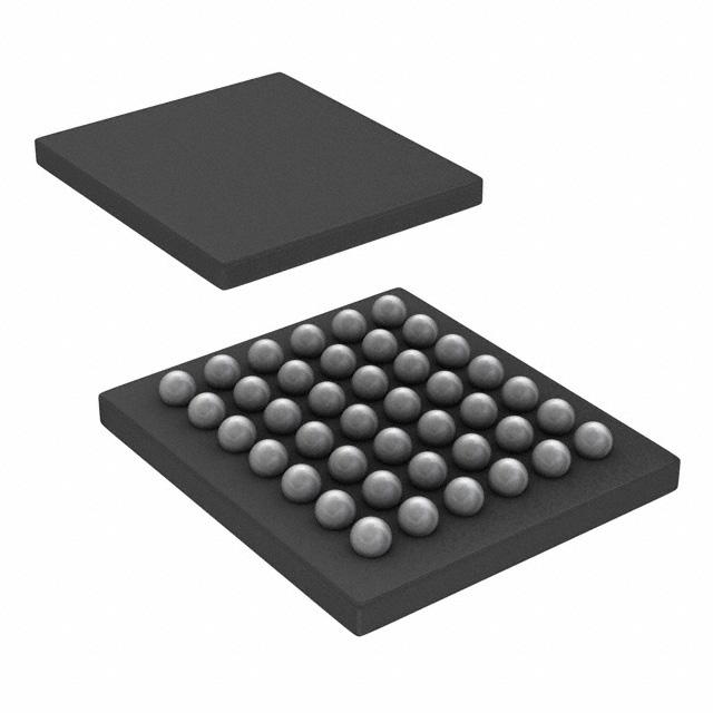


 工商网监
湘ICP备2023018690号
工商网监
湘ICP备2023018690号
