FM24W256
256-Kbit (32 K × 8) Serial (I2C) F-RAM
256-Kbit (32 K × 8) Serial (I2C) F-RAM
Features
■
■
Functional Description
256-Kbit ferroelectric random access memory (F-RAM)
logically organized as 32 K × 8
14
❐ High-endurance 100 trillion (10 ) read/writes
❐ 151-year data retention (See the Data Retention and
Endurance table)
❐ NoDelay™ writes
❐ Advanced high-reliability ferroelectric process
The FM24W256 is a 256-Kbit nonvolatile memory employing an
advanced ferroelectric process. A ferroelectric random access
memory or F-RAM is nonvolatile and performs reads and writes
similar to a RAM. It provides reliable data retention for 151 years
while eliminating the complexities, overhead, and system-level
reliability problems caused by EEPROM and other nonvolatile
memories.
Fast 2-wire Serial interface (I2C)
❐ Up to 1-MHz frequency
2
❐ Direct hardware replacement for serial (I C) EEPROM
❐ Supports legacy timings for 100 kHz and 400 kHz
Unlike EEPROM, the FM24W256 performs write operations at
bus speed. No write delays are incurred. Data is written to the
memory array immediately after each byte is successfully
transferred to the device. The next bus cycle can commence
without the need for data polling. In addition, the product offers
substantial write endurance compared with other nonvolatile
memories. Also, F-RAM exhibits much lower power during writes
than EEPROM since write operations do not require an internally
elevated power supply voltage for write circuits. The FM24W256
is capable of supporting 1014 read/write cycles, or 100 million
times more write cycles than EEPROM.
■
Low power consumption
❐ 100 A active current at 100 kHz
❐ 15 A (typ) standby current
■
Wide voltage operation: VDD = 2.7 V to 5.5 V
■
Industrial temperature: –40 C to +85 C
■
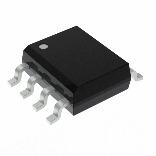
8-pin small outline integrated circuit (SOIC) package
■
Restriction of hazardous substances (RoHS) compliant
These capabilities make the FM24W256 ideal for nonvolatile
memory applications, requiring frequent or rapid writes.
Examples range from data logging, where the number of write
cycles may be critical, to demanding industrial controls where the
long write time of EEPROM can cause data loss. The
combination of features allows more frequent data writing with
less overhead for the system.
The FM24W256 provides substantial benefits to users of serial
(I2C) EEPROM as a hardware drop-in replacement. The device
specifications are guaranteed over an industrial temperature
range of –40 C to +85 C.
For a complete list of related documentation, click here.
Logic Block Diagram
Address
Latch
Counter
32 K x 8
F-RAM Array
15
8
SDA
Serial to Parallel
Converter
Data Latch
8
SCL
WP
Control Logic
A2-A0
Cypress Semiconductor Corporation
Document Number: 001-84464 Rev. *K
•
198 Champion Court
•
San Jose, CA 95134-1709
•
408-943-2600
Revised April 28, 2017
�FM24W256
Contents
Pinout ................................................................................ 3
Pin Definitions .................................................................. 3
Functional Overview ........................................................ 4
Memory Architecture ........................................................ 4
I2C Interface ...................................................................... 4
STOP Condition (P) ..................................................... 4
START Condition (S) ................................................... 4
Data/Address Transfer ................................................ 5
Acknowledge / No-acknowledge ................................. 5
Slave Device Address ................................................. 6
Addressing Overview .................................................. 6
Data Transfer .............................................................. 6
Memory Operation ............................................................ 6
Write Operation ........................................................... 6
Read Operation ........................................................... 7
Maximum Ratings ............................................................. 9
Operating Range ............................................................... 9
DC Electrical Characteristics .......................................... 9
Data Retention and Endurance ..................................... 10
Document Number: 001-84464 Rev. *K
Capacitance .................................................................... 10
Thermal Resistance ........................................................ 10
AC Test Loads and Waveforms ..................................... 10
AC Test Conditions ........................................................ 10
AC Switching Characteristics ....................................... 11
Power Cycle Timing ....................................................... 12
Ordering Information ...................................................... 13
Ordering Code Definitions ......................................... 13
Package Diagrams .......................................................... 14
Acronyms ........................................................................ 16
Document Conventions ................................................. 16
Units of Measure ....................................................... 16
Document History Page ................................................. 17
Sales, Solutions, and Legal Information ...................... 18
Worldwide Sales and Design Support ....................... 18
Products .................................................................... 18
PSoC® Solutions ...................................................... 18
Cypress Developer Community ................................. 18
Technical Support ..................................................... 18
Page 2 of 18
�FM24W256
Pinout
Figure 1. 8-pin SOIC pinout
A0
1
A1
2
A2
3
VSS
4
Top View
not to scale
8
VDD
7
WP
6
SCL
5
SDA
Pin Definitions
Pin Name
I/O Type
Description
A2-A0
Input
Device Select Address 2-0. These pins are used to select one of up to 8 devices of the same type on
the same I2C bus. To select the device, the address value on the three pins must match the corresponding bits contained in the slave address. The address pins are pulled down internally.
SDA
Input/Output Serial Data/Address. This is a bi-directional pin for the I2C interface. It is open-drain and is intended
to be wire-AND'd with other devices on the I2C bus. The input buffer incorporates a Schmitt trigger for
noise immunity and the output driver includes slope control for falling edges. An external pull-up resistor
is required.
SCL
Input
Serial Clock. The serial clock pin for the I2C interface. Data is clocked out of the device on the falling
edge, and into the device on the rising edge. The SCL input also incorporates a Schmitt trigger input
for noise immunity.
WP
Input
Write Protect. When tied to VDD, addresses in the entire memory map will be write-protected. When
WP is connected to ground, all addresses are write enabled. This pin is pulled down internally.
VSS
Power supply Ground for the device. Must be connected to the ground of the system.
VDD
Power supply Power supply input to the device.
Document Number: 001-84464 Rev. *K
Page 3 of 18
�FM24W256
Functional Overview
a new bus transaction can be shifted into the device, a write
operation is complete. This is explained in more detail in the
interface section.
The FM24W256 is a serial F-RAM memory. The memory array
is logically organized as 32,768 × 8 bits and is accessed using
an industry-standard I2C interface. The functional operation of
the F-RAM is similar to serial (I2C) EEPROM. The major
difference between the FM24W256 and a serial (I2C) EEPROM
with the same pinout is the F-RAM's superior write performance,
high endurance, and low power consumption.
I2C Interface
The FM24W256 employs a bi-directional I2C bus protocol using
few pins or board space. Figure 2 illustrates a typical system
configuration using the FM24W256 in a microcontroller-based
system. The industry standard I2C bus is familiar to many users
but is described in this section.
Memory Architecture
By convention, any device that is sending data onto the bus is
the transmitter while the target device for this data is the receiver.
The device that is controlling the bus is the master. The master
is responsible for generating the clock signal for all operations.
Any device on the bus that is being controlled is a slave. The
FM24W256 is always a slave device.
When accessing the FM24W256, the user addresses 32K
locations of eight data bits each. These eight data bits are shifted
in or out serially. The addresses are accessed using the I2C
protocol, which includes a slave address (to distinguish other
non-memory devices) and a two-byte address. The upper bit of
the address range is 'don't care' value. The complete address of
15 bits specifies each byte address uniquely.
The bus protocol is controlled by transition states in the SDA and
SCL signals. There are four conditions including START, STOP,
data bit, or acknowledge. Figure 3 and Figure 4 illustrates the
signal conditions that specify the four states. Detailed timing
diagrams are shown in the electrical specifications section.
The access time for the memory operation is essentially zero,
beyond the time needed for the serial protocol. That is, the
memory is read or written at the speed of the I2C bus. Unlike a
serial (I2C) EEPROM, it is not necessary to poll the device for a
ready condition because writes occur at bus speed. By the time
Figure 2. System Configuration using Serial (I2C) nvSRAM
RPmin = (VDD - VOLmax) / IOL
V DD
RPmax = tr / (0.8473 * Cb)
SDA
Microcontroller
SCL
V DD
V DD
A0
SCL
A0
SCL
A0
SCL
A1
SDA
A1
SDA
A1
SDA
WP
A2
WP
A2
#0
#1
A2
WP
#7
STOP Condition (P)
START Condition (S)
A STOP condition is indicated when the bus master drives SDA
from LOW to HIGH while the SCL signal is HIGH. All operations
using the FM24W256 should end with a STOP condition. If an
operation is in progress when a STOP is asserted, the operation
will be aborted. The master must have control of SDA in order to
assert a STOP condition.
A START condition is indicated when the bus master drives SDA
from HIGH to LOW while the SCL signal is HIGH. All commands
should be preceded by a START condition. An operation in
progress can be aborted by asserting a START condition at any
time. Aborting an operation using the START condition will ready
the FM24W256 for a new operation.
If during operation the power supply drops below the specified
VDD minimum, the system should issue a START condition prior
to performing another operation.
Document Number: 001-84464 Rev. *K
Page 4 of 18
�FM24W256
Figure 3. START and STOP Conditions
full pagewidth
SDA
SDA
SCL
SCL
S
P
STOP Condition
START Condition
Figure 4. Data Transfer on the I2C Bus
handbook, full pagewidth
P
SDA
Acknowledgement
signal from slave
MSB
SCL
S
1
2
7
9
8
1
Acknowledgement
signal from receiver
2
3
4-8
ACK
START
condition
9
ACK
All data transfers (including addresses) take place while the SCL
signal is HIGH. Except under the three conditions described
above, the SDA signal should not change while SCL is HIGH.
Acknowledge / No-acknowledge
The acknowledge takes place after the 8th data bit has been
transferred in any transaction. During this state the transmitter
should release the SDA bus to allow the receiver to drive it. The
receiver drives the SDA signal LOW to acknowledge receipt of
the byte. If the receiver does not drive SDA LOW, the condition
is a no-acknowledge and the operation is aborted.
S
or
P
STOP or
START
condition
Byte complete
Data/Address Transfer
S
The receiver would fail to acknowledge for two distinct reasons.
First is that a byte transfer fails. In this case, the no-acknowledge
ceases the current operation so that the device can be
addressed again. This allows the last byte to be recovered in the
event of a communication error.
Second and most common, the receiver does not acknowledge
to deliberately end an operation. For example, during a read
operation, the FM24W256 will continue to place data onto the
bus as long as the receiver sends acknowledges (and clocks).
When a read operation is complete and no more data is needed,
the receiver must not acknowledge the last byte. If the receiver
acknowledges the last byte, this will cause the FM24W256 to
attempt to drive the bus on the next clock while the master is
sending a new command such as STOP.
Figure 5. Acknowledge on the I2C Bus
handbook, full pagewidth
DATA OUTPUT
BY MASTER
No Acknowledge
DATA OUTPUT
BY SLAVE
Acknowledge
SCL FROM
MASTER
1
2
8
9
S
START
Condition
Document Number: 001-84464 Rev. *K
Clock pulse for
acknowledgement
Page 5 of 18
�FM24W256
Slave Device Address
sequential byte. If the acknowledge is not sent, the FM24W256
will end the read operation. For a write operation, the FM24W256
will accept 8 data bits from the master then send an
acknowledge. All data transfer occurs MSB (most significant bit)
first.
The first byte that the FM24W256 expects after a START
condition is the slave address. As shown in Figure 6, the slave
address contains the device type or slave ID, the device select
address bits, and a bit that specifies if the transaction is a read
or a write.
Memory Operation
Bits 7-4 are the device type (slave ID) and should be set to 1010b
for the FM24W256. These bits allow other function types to
reside on the I2C bus within an identical address range. Bits 3-1
are the device select address bits. They must match the corresponding value on the external address pins to select the device.
Up to eight FM24W256 devices can reside on the same I2C bus
by assigning a different address to each. Bit 0 is the read/write
bit (R/W). R/W = ‘1’ indicates a read operation and R/W = ‘0’
indicates a write operation.
The FM24W256 is designed to operate in a manner very similar
to other I2C interface memory products. The major differences
result from the higher performance write capability of F-RAM
technology. These improvements result in some differences
between the FM24W256 and a similar configuration EEPROM
during writes. The complete operation for both writes and reads
is explained below.
Write Operation
Figure 6. Memory Slave Device Address
MSB
handbook, halfpage
1
All writes begin with a slave address, then a memory address.
The bus master indicates a write operation by setting the LSB of
the slave address (R/W bit) to a '0'. After addressing, the bus
master sends each byte of data to the memory and the memory
generates an acknowledge condition. Any number of sequential
bytes may be written. If the end of the address range is reached
internally, the address counter will wrap from 7FFFh to 0000h.
LSB
0
1
Slave ID
0
A2
A1
A0 R/W
Device Select
Addressing Overview
Unlike other nonvolatile memory technologies, there is no
effective write delay with F-RAM. Since the read and write
access times of the underlying memory are the same, the user
experiences no delay through the bus. The entire memory cycle
occurs in less time than a single bus clock. Therefore, any
operation including read or write can occur immediately following
a write. Acknowledge polling, a technique used with EEPROMs
to determine if a write is complete is unnecessary and will always
return a ready condition.
After the FM24W256 (as receiver) acknowledges the slave
address, the master can place the memory address on the bus
for a write operation. The address requires two bytes. The
complete 15-bit address is latched internally. Each access
causes the latched address value to be incremented automatically. The current address is the value that is held in the latch;
either a newly written value or the address following the last
access. The current address will be held for as long as power
remains or until a new value is written. Reads always use the
current address. A random read address can be loaded by
beginning a write operation as explained below.
Internally, an actual memory write occurs after the 8th data bit is
transferred. It will be complete before the acknowledge is sent.
Therefore, if the user desires to abort a write without altering the
memory contents, this should be done using START or STOP
condition prior to the 8th data bit. The FM24W256 uses no page
buffering.
After transmission of each data byte, just prior to the
acknowledge, the FM24W256 increments the internal address
latch. This allows the next sequential byte to be accessed with
no additional addressing. After the last address (7FFFh) is
reached, the address latch will roll over to 0000h. There is no
limit to the number of bytes that can be accessed with a single
read or write operation.
The memory array can be write-protected using the WP pin.
Setting the WP pin to a HIGH condition (VDD) will write-protect
all addresses. The FM24W256 will not acknowledge data bytes
that are written to protected addresses. In addition, the address
counter will not increment if writes are attempted to these
addresses. Setting WP to a LOW state (VSS) will disable the write
protect. WP is pulled down internally.
Data Transfer
After the address bytes have been transmitted, data transfer
between the bus master and the FM24W256 can begin. For a
read operation the FM24W256 will place 8 data bits on the bus
then wait for an acknowledge from the master. If the
acknowledge occurs, the FM24W256 will transfer the next
Figure 7 and Figure 8 below illustrate a single-byte and
multiple-byte write cycles.
Figure 7. Single-Byte Write
By Master
Start
S
Stop
Address & Data
Slave Address
By F-RAM
Document Number: 001-84464 Rev. *K
0 A
Address MSB
A
Address LSB
A
Data Byte
A
P
Acknowledge
Page 6 of 18
�FM24W256
Figure 8. Multi-Byte Write
Start
Stop
Address & Data
By Master
S
Slave Address
0 A
Address MSB
By F-RAM
A
Address LSB
A
Data Byte
A
Data Byte
A
P
Acknowledge
Read Operation
There are two basic types of read operations. They are current
address read and selective address read. In a current address
read, the FM24W256 uses the internal address latch to supply
the address. In a selective read, the user performs a procedure
to set the address to a specific value.
Current Address & Sequential Read
As mentioned above the FM24W256 uses an internal latch to
supply the address for a read operation. A current address read
uses the existing value in the address latch as a starting place
for the read operation. The system reads from the address
immediately following that of the last operation.
To perform a current address read, the bus master supplies a
slave address with the LSB set to a '1'. This indicates that a read
operation is requested. After receiving the complete slave
address, the FM24W256 will begin shifting out data from the
current address on the next clock. The current address is the
value held in the internal address latch.
Beginning with the current address, the bus master can read any
number of bytes. Thus, a sequential read is simply a current
address read with multiple byte transfers. After each byte the
internal address counter will be incremented.
Note Each time the bus master acknowledges a byte, this
indicates that the FM24W256 should read out the next
sequential byte.
There are four ways to properly terminate a read operation.
Failing to properly terminate the read will most likely create a bus
contention as the FM24W256 attempts to read out additional
data onto the bus. The four valid methods are:
1. The bus master issues a no-acknowledge in the 9th clock
cycle and a STOP in the 10th clock cycle. This is illustrated in
the diagrams below. This is preferred.
2. The bus master issues a no-acknowledge in the 9th clock
cycle and a START in the 10th.
3. The bus master issues a STOP in the 9th clock cycle.
4. The bus master issues a START in the 9th clock cycle.
Figure 9. Current Address Read
By Master
Start
No
Acknowledge
Address
Stop
S
Slave Address
By F-RAM
1 A
Acknowledge
Data Byte
1
P
Data
Figure 10. Sequential Read
By Master
Start
Address
No
Acknowledge
Acknowledge
Stop
S
Slave Address
By F-RAM
Document Number: 001-84464 Rev. *K
1 A
Acknowledge
Data Byte
A
Data Byte
1 P
Data
Page 7 of 18
�FM24W256
Selective (Random) Read
There is a simple technique that allows a user to select a random
address location as the starting point for a read operation. This
involves using the first three bytes of a write operation to set the
internal address followed by subsequent read operations.
To perform a selective read, the bus master sends out the slave
address with the LSB (R/W) set to 0. This specifies a write
operation. According to the write protocol, the bus master then
sends the address bytes that are loaded into the internal address
latch. After the FM24W256 acknowledges the address, the bus
master issues a START condition. This simultaneously aborts
the write operation and allows the read command to be issued
with the slave address LSB set to a '1'. The operation is now a
current address read.
Figure 11. Selective (Random) Read
Start
Address
By Master
Start
No
Acknowledge
Address
Stop
S
Slave Address
0 A
By F-RAM
Document Number: 001-84464 Rev. *K
Address MSB
A
Address LSB
Acknowledge
A
S
Slave Address
1 A
Data Byte
1 P
Data
Page 8 of 18
�FM24W256
Maximum Ratings
Exceeding maximum ratings may shorten the useful life of the
device. These user guidelines are not tested.
Storage temperature ................................ –55 C to +125 C
Surface mount lead soldering
temperature (10 seconds) ....................................... +260 C
Electrostatic Discharge Voltage
Human Body Model (AEC-Q100-002 Rev. E) .................. 3.5 kV
Charged Device Model (AEC-Q100-011 Rev. B) ............. 1.25 kV
Maximum accumulated storage time
At 125 °C ambient temperature ................................. 1000 h
At 85 °C ambient temperature ................................ 10 Years
Latch-up current .................................................... > 140 mA
Ambient temperature
with power applied ................................... –55 °C to +125 °C
* Exception: The “VIN < VDD + 1.0 V” restriction does not apply
to the SCL and SDA inputs.
Supply voltage on VDD relative to VSS .........–1.0 V to +7.0 V
Operating Range
Machine Model (AEC-Q100-003 Rev. E) ............................ 200 V
Input voltage .......... –1.0 V to + 7.0 V and VIN < VDD + 1.0 V
Range
Ambient Temperature (TA)
VDD
DC voltage applied to outputs
in High-Z state .................................... –0.5 V to VDD + 0.5 V
Industrial
–40 C to +85 C
2.7 V to 5.5 V
Transient voltage (< 20 ns) on
any pin to ground potential ................. –2.0 V to VDD + 2.0 V
Package power dissipation
capability (TA = 25 °C) ................................................. 1.0 W
DC Electrical Characteristics
Over the Operating Range
Parameter
Description
VDD
Power supply
IDD
Average VDD current
Test Conditions
SCL toggling
between
VDD – 0.3 V and VSS,
other inputs VSS or
VDD – 0.3 V.
Min
Typ [1]
Max
Unit
2.7
3.3
5.5
V
fSCL = 100 kHz
–
–
100
A
fSCL = 400 kHz
–
–
200
A
fSCL = 1 MHz
–
–
400
A
ISB
Standby current
SCL = SDA = VDD. All other inputs VSS
or VDD. Stop command issued.
–
15
30
A
ILI
Input leakage current
(Except WP and A2-A0)
VSS < VIN < VDD
–1
–
+1
A
Input leakage current
(for WP and A2-A0)
VSS < VIN < VDD
–1
–
+100
A
ILO
Output leakage current
VSS < VIN < VDD
VIH
Input HIGH voltage
VIL
Input LOW voltage
VOL
Output LOW voltage
IOL = 3 mA
Rin[2]
Input resistance (WP, A2-A0)
–1
–
+1
A
0.7 × VDD
–
VDD + 0.3
V
– 0.3
–
0.3 × VDD
V
–
–
0.4
V
For VIN = VIL (Max)
40
–
–
k
For VIN = VIH (Min)
1
–
–
M
Notes
1. Typical values are at 25 °C, VDD = VDD (typ). Not 100% tested.
2. The input pull-down circuit is strong (40 k) when the input voltage is below VIL and weak (1 M) when the input voltage is above VIH.
Document Number: 001-84464 Rev. *K
Page 9 of 18
�FM24W256
Data Retention and Endurance
Parameter
TDR
NVC
Description
Test condition
TA = 85 C
Data retention
Endurance
Min
Max
Unit
10
–
Years
TA = 75 C
38
–
TA = 65 C
151
–
Over operating temperature
1014
–
Cycles
Capacitance
Parameter [3]
Description
Test Conditions
CO
Output pin capacitance (SDA)
CI
Input pin capacitance
Max
Unit
8
pF
6
pF
TA = 25 C, f = 1 MHz, VDD = VDD(typ)
Thermal Resistance
Parameter [3]
JA
JC
Description
Thermal resistance
(junction to ambient)
Thermal resistance
(junction to case)
Test Conditions
8-pin SOIC
Unit
Test conditions follow standard test methods
and procedures for measuring thermal
impedance, per EIA / JESD51.
141
C/W
43
C/W
AC Test Loads and Waveforms
Figure 12. AC Test Loads and Waveforms
5.5 V
1.7 k
OUTPUT
100 pF
AC Test Conditions
Input pulse levels .................................10% and 90% of VDD
Input rise and fall times .................................................10 ns
Input and output timing reference levels ................0.5 × VDD
Output load capacitance ............................................ 100 pF
Note
3. These parameters are guaranteed by design and are not tested.
Document Number: 001-84464 Rev. *K
Page 10 of 18
�FM24W256
AC Switching Characteristics
Over the Operating Range
Alt.
Parameter
Parameter[4]
Description
fSCL[5]
SCL clock frequency
Min
Max
Min
Max
Min
Max
Unit
–
0.1
–
0.4
–
1.0
MHz
tSU; STA
Start condition setup for repeated Start
4.7
–
0.6
–
0.25
–
s
tHD;STA
Start condition hold time
4.0
–
0.6
–
0.25
–
s
tLOW
Clock LOW period
4.7
–
1.3
–
0.6
–
s
tHIGH
Clock HIGH period
4.0
–
0.6
–
0.4
–
s
tSU;DAT
tSU;DATA
Data in setup
250
–
100
–
100
–
ns
tHD;DAT
tHD;DATA
Data in hold
0
–
0
–
0
–
ns
Data output hold (from SCL @ VIL)
0
–
0
–
0
–
ns
–
1000
–
300
–
300
ns
tDH
[6]
tr
Input rise time
tF[6]
tf
Input fall time
tR
–
300
–
300
–
100
ns
4.0
–
0.6
–
0.25
–
s
SCL LOW to SDA Data Out Valid
–
3
–
0.9
–
0.55
s
tBUF
Bus free before new transmission
4.7
–
1.3
–
0.5
–
s
tSP
Noise suppression time constant on SCL, SDA
–
50
–
50
–
50
ns
STOP condition setup
tSU;STO
tVD;DATA
tAA
Figure 13. Read Bus Timing Diagram
tR
`
tF
tHIGH
tSP
tLOW
tSP
SCL
tSU:SDA
1/fSCL
tBUF
tHD:DAT
tSU:DAT
SDA
tDH
tAA
Stop Start
Start
Acknowledge
Figure 14. Write Bus Timing Diagram
tHD:DAT
SCL
tHD:STA
tSU:STO
tSU:DAT
tAA
SDA
Start
Stop Start
Acknowledge
Notes
4. Test conditions assume signal transition time of 10 ns or less, timing reference levels of VDD/2, input pulse levels of 0 to VDD(typ), and output loading of the specified
IOL and load capacitance shown in Figure 12.
5. The speed-related specifications are guaranteed characteristic points along a continuous curve of operation from DC to fSCL (max).
6. These parameters are guaranteed by design and are not tested.
Document Number: 001-84464 Rev. *K
Page 11 of 18
�FM24W256
Power Cycle Timing
Over the Operating Range
Parameter
Description
Min
Max
Unit
tPU
Power-up VDD(min) to first access (START condition)
1
–
ms
tPD
Last access (STOP condition) to power-down (VDD(min))
0
–
µs
tVR [7, 8]
VDD power-up ramp rate
30
–
µs/V
tVF [7, 8]
VDD power-down ramp rate
30
–
µs/V
VDD
~
~
Figure 15. Power Cycle Timing
VDD(min)
tVR
SDA
I2 C START
tVF
tPD
~
~
tPU
VDD(min)
I2 C STOP
Notes
7. Slope measured at any point on the VDD waveform.
8. Guaranteed by design.
Document Number: 001-84464 Rev. *K
Page 12 of 18
�FM24W256
Ordering Information
Package
Diagram
Ordering Code
FM24W256-G
Package Type
51-85066
8-pin SOIC
001-85261
8-pin SOIC
Operating
Range
Industrial
FM24W256-GTR
FM24W256-EG
FM24W256-EGTR
All these parts are Pb-free. Contact your local Cypress sales representative for availability of these parts.
Ordering Code Definitions
FM 24 W 256 - G
TR
Option:
blank = Standard; TR = Tape and Reel
Package Type:
G = 8-pin SOIC; EG = EIAJ SOIC
Density: 256 = 256-Kbit
Voltage: W = 2.7 V to 5.5 V
I2C F-RAM
Cypress
Document Number: 001-84464 Rev. *K
Page 13 of 18
�FM24W256
Package Diagrams
Figure 16. 8-pin SOIC (150 Mils) Package Outline, 51-85066
51-85066 *H
Document Number: 001-84464 Rev. *K
Page 14 of 18
�FM24W256
Package Diagrams (continued)
Figure 17. 8-pin SOIC (208 Mils) Package Outline, 001-85261
001-85261 **
Document Number: 001-84464 Rev. *K
Page 15 of 18
�FM24W256
Acronyms
Acronym
Document Conventions
Description
Units of Measure
ACK
Acknowledge
CMOS
Complementary Metal Oxide Semiconductor
°C
degree Celsius
EIA
Electronic Industries Alliance
I2C
Hz
hertz
Inter-Integrated Circuit
Kb
1024 bit
I/O
Input/Output
kHz
kilohertz
JEDEC
Joint Electron Devices Engineering Council
k
kilohm
LSB
Least Significant Bit
MHz
megahertz
MSB
Most Significant Bit
M
megaohm
NACK
No Acknowledge
A
microampere
RoHS
Restriction of Hazardous Substances
s
microsecond
R/W
Read/Write
mA
milliampere
SCL
Serial Clock Line
ms
millisecond
SDA
Serial Data Access
ns
nanosecond
SOIC
Small Outline Integrated Circuit
ohm
WP
Write Protect
%
percent
pF
picofarad
V
volt
W
watt
Document Number: 001-84464 Rev. *K
Symbol
Unit of Measure
Page 16 of 18
�FM24W256
Document History Page
Document Title: FM24W256, 256-Kbit (32 K × 8) Serial (I2C) F-RAM
Document Number: 001-84464
Rev.
ECN No.
Submission
Date
Orig. of
Change
**
3902082
02/25/2013
GVCH
New spec
*A
3924523
03/07/2013
GVCH
Changed tPU timing parameter from 10 ms to 1 ms
Changed RIN (high) spec from 4 Mto 1 M
Description of Change
*B
3985098
05/09/2013
GVCH
Updated SOIC package marking scheme
*C
4014247
05/29/2013
GVCH
Added Appendix A - Errata for FM24W256
*D
4045469
06/30/2013
GVCH
All errata items are fixed and the errata is removed.
*E
4283420
02/19/2014
GVCH
Converted to Cypress standard format
Changed datasheet status from “Preliminary to Final”
Updated Maximum Ratings table
- Removed Moisture Sensitivity Level (MSL)
- Added junction temperature and latch up current
Added Input leakage current (ILI) for WP and A2-A0
Updated Data Retention and Endurance table
Added Thermal Resistance table
Removed Package Marking Scheme (top mark)
*F
4272607
03/12/2014
GVCH
Typo fixed (Power Cycle Timing): Invalid tREC spec removed
*G
4562106
11/05/2014
GVCH
Updated Functional Description:
Added “For a complete list of related documentation, click here.” at the end.
*H
4781114
05/29/2015
GVCH
Updated Ordering Information:
Fixed Typo (Replaced “001-85066” with “51-85066” in “Package Diagram”
column).
Updated Package Diagrams:
spec 51-85066 – Changed revision from *F to *G.
Updated to new template.
*I
4874738
08/06/2015
*J
4951762
10/07/2015
*K
5718043
04/28/2017
Document Number: 001-84464 Rev. *K
ZSK / PSR Updated Maximum Ratings:
Removed “Maximum junction temperature”.
Added “Maximum accumulated storage time”.
Added “Ambient temperature with power applied”.
LIZB /
GVCH
Updated Ordering Information:
No change in part numbers.
Removed “Not recommended for new designs” in “Package Type” column
corresponding to “FM24W256-EG” and “FM24W256-EGTR”.
Updated Package Diagrams:
spec 51-85066 – Changed revision from *G to *H.
AESATMP8 Updated logo and Copyright.
Page 17 of 18
�FM24W256
Sales, Solutions, and Legal Information
Worldwide Sales and Design Support
Cypress maintains a worldwide network of offices, solution centers, manufacturer’s representatives, and distributors. To find the office
closest to you, visit us at Cypress Locations.
PSoC® Solutions
Products
ARM® Cortex® Microcontrollers
Automotive
cypress.com/arm
cypress.com/automotive
Clocks & Buffers
Interface
cypress.com/clocks
cypress.com/interface
Internet of Things
Memory
cypress.com/iot
cypress.com/memory
Microcontrollers
cypress.com/mcu
PSoC
cypress.com/psoc
Power Management ICs
Cypress Developer Community
Forums | WICED IOT Forums | Projects | Video | Blogs |
Training | Components
Technical Support
cypress.com/support
cypress.com/pmic
Touch Sensing
cypress.com/touch
USB Controllers
Wireless Connectivity
PSoC 1 | PSoC 3 | PSoC 4 | PSoC 5LP | PSoC 6
cypress.com/usb
cypress.com/wireless
© Cypress Semiconductor Corporation, 2013-2017. This document is the property of Cypress Semiconductor Corporation and its subsidiaries, including Spansion LLC (“Cypress”). This document,
including any software or firmware included or referenced in this document (“Software”), is owned by Cypress under the intellectual property laws and treaties of the United States and other countries
worldwide. Cypress reserves all rights under such laws and treaties and does not, except as specifically stated in this paragraph, grant any license under its patents, copyrights, trademarks, or other
intellectual property rights. If the Software is not accompanied by a license agreement and you do not otherwise have a written agreement with Cypress governing the use of the Software, then Cypress
hereby grants you a personal, non-exclusive, nontransferable license (without the right to sublicense) (1) under its copyright rights in the Software (a) for Software provided in source code form, to
modify and reproduce the Software solely for use with Cypress hardware products, only internally within your organization, and (b) to distribute the Software in binary code form externally to end users
(either directly or indirectly through resellers and distributors), solely for use on Cypress hardware product units, and (2) under those claims of Cypress's patents that are infringed by the Software (as
provided by Cypress, unmodified) to make, use, distribute, and import the Software solely for use with Cypress hardware products. Any other use, reproduction, modification, translation, or compilation
of the Software is prohibited.
TO THE EXTENT PERMITTED BY APPLICABLE LAW, CYPRESS MAKES NO WARRANTY OF ANY KIND, EXPRESS OR IMPLIED, WITH REGARD TO THIS DOCUMENT OR ANY SOFTWARE
OR ACCOMPANYING HARDWARE, INCLUDING, BUT NOT LIMITED TO, THE IMPLIED WARRANTIES OF MERCHANTABILITY AND FITNESS FOR A PARTICULAR PURPOSE. To the extent
permitted by applicable law, Cypress reserves the right to make changes to this document without further notice. Cypress does not assume any liability arising out of the application or use of any
product or circuit described in this document. Any information provided in this document, including any sample design information or programming code, is provided only for reference purposes. It is
the responsibility of the user of this document to properly design, program, and test the functionality and safety of any application made of this information and any resulting product. Cypress products
are not designed, intended, or authorized for use as critical components in systems designed or intended for the operation of weapons, weapons systems, nuclear installations, life-support devices or
systems, other medical devices or systems (including resuscitation equipment and surgical implants), pollution control or hazardous substances management, or other uses where the failure of the
device or system could cause personal injury, death, or property damage (“Unintended Uses”). A critical component is any component of a device or system whose failure to perform can be reasonably
expected to cause the failure of the device or system, or to affect its safety or effectiveness. Cypress is not liable, in whole or in part, and you shall and hereby do release Cypress from any claim,
damage, or other liability arising from or related to all Unintended Uses of Cypress products. You shall indemnify and hold Cypress harmless from and against all claims, costs, damages, and other
liabilities, including claims for personal injury or death, arising from or related to any Unintended Uses of Cypress products.
Cypress, the Cypress logo, Spansion, the Spansion logo, and combinations thereof, WICED, PSoC, CapSense, EZ-USB, F-RAM, and Traveo are trademarks or registered trademarks of Cypress in
the United States and other countries. For a more complete list of Cypress trademarks, visit cypress.com. Other names and brands may be claimed as property of their respective owners.
Document Number: 001-84464 Rev. *K
Revised April 28, 2017
Page 18 of 18
�


 工商网监
湘ICP备2023018690号
工商网监
湘ICP备2023018690号

