IS26KS512S/256S/128S
IS26KL512S/256S/128S
512Mb/256Mb/128Mb
HyperFlash™ Family Non-Volatile Memory
DATA SHEET
Integrated Silicon Solution, Inc.- www.issi.com
Rev.A3
08/10/2017
1
�IS26KS128S/256S/512S
IS26KL128S/256S/512S
HyperFlash™ Family Non-Volatile
Memory
AUGUST 2017
IS26KS512S / IS26KL512S 512 Mbit (64 Mbyte)
IS26KS256S / IS26KL256S 256 Mbit (32 Mbyte)
IS26KS128S / IS26KL128S 128 Mbit (16 Mbyte)
CMOS 1.8 Volt or 3.0 Volt Core and I/O
Features
3.0V I/O, 11 bus signals
– Single ended clock
1.8V I/O, 12 bus signals
– Differential clock (CK, CK#)
Chip Select (CS#)
8-bit data bus (DQ[7:0])
Read-Write Data Strobe (RWDS)
– HyperFlash™ memories use RWDS only as a Read Data
Strobe
Up to 333 MB/s sustained read throughput
Double-Data Rate (DDR) – two data transfers per clock
166-MHz clock rate (333 MB/s) at 1.8V VCC
100-MHz clock rate (200 MB/s) at 3.0V VCC
96-ns initial random read access time
– Initial random access read latency: 5 to 16 clock cycles
Sequential burst transactions
Configurable Burst Characteristics
– Wrapped burst lengths:
– 16 bytes (8 clocks)
– 32 bytes (16 clocks)
– 64 bytes (32 clocks)
– Linear burst
– Hybrid option — one wrapped burst followed by linear burst
– Wrapped or linear burst type selected in each transaction
– Configurable output drive strength
Low Power Modes
– Active Clock Stop During Read: 12 mA, no wake-up
required
– Standby: 25 µA (typical), no wake-up required
– Deep Power-Down: 8 µA (typical)
– 300 µs wake-up required
Integrated Silicon Solution, Inc.- www.issi.com
Rev.A3
08/10/2017
INT# output to generate external interrupt
– Busy to Ready Transition
– ECC detection
RSTO# output to generate system level power-on reset
– User configurable RSTO# Low period
512-byte Program Buffer
Sector Erase
– Uniform 256-kB sectors
– Optional Eight 4-kB Parameter Sectors (32 kB total)
Advanced Sector Protection
– Volatile and non-volatile protection methods for each
sector
Separate 1024-byte one-time program array
Operating Temperature
– Industrial (–40°C to +85°C)
– Extended (–40°C to +105°C)
– Extended + (–40°C to +125°C)
– Automotive, AEC-Q100 Grade A1 (–40°C to +85°C)
– Automotive, AEC-Q100 Grade A2 (–40°C to +105°C)
– Automotive, AEC-Q100 Grade A3 (–40°C to +125°C)
ISO/TS16949 and AEC Q100 Certified
Endurance
– 100,000 program/erase cycles
Retention
– 20 year data retention
Erase and Program Current
– Max Peak 100 mA
Packaging Options
– 24-Ball FBGA
Additional Features
– ECC 1-bit correction, 2-bit detection
– CRC (Check-value Calculation)
2
�IS26KS128S/256S/512S
IS26KL128S/256S/512S
Performance Summary
Read Access Timings
Maximum Clock Rate at 1.8V VCC/VCCQ
166 MHz
Maximum Clock Rate at 3.0V VCC/VCCQ
100 MHz
Maximum Access Time, (tACC)
96 ns
Maximum CS# Access Time to First Word @ 166 MHz
118 ns
Typical Program / Erase Times
Single Word Programming (2B = 16b)
500 µs (~4 kB/s)
Write Buffer Programming (512B = 4096b)
475 µs (~1 MB/s)
Sector Erase Time (256 kB = 2 Mb)
930 ms (~282 kB/s)
Typical Current Consumption
Burst Read (Continuous Read at 166 MHz)
80 mA
Power-On Reset
80 mA
Sector Erase Current
60 mA
Write Buffer Programming Current
60 mA
Standby (CS# = High)
25 µA
Deep Power-Down (CS# = High, 85°C)
Integrated Silicon Solution, Inc.- www.issi.com
Rev.A3
08/10/2017
30 µA (512 Mb)
4 µA (all other densities)
3
�IS26KS128S/256S/512S
IS26KL128S/256S/512S
Contents
1.
1.1
1.2
General Description.................................................... 4
DDR Center Aligned Read Strobe Functionality
(DCARS)....................................................................... 7
Error Detection and Correction Functionality................ 7
2.
2.1
Connection Diagram...................................................10
FBGA 24-Ball 5 x 5 Array Footprint..............................10
3.
Signal Description .................................................... 11
4.
4.1
4.2
4.3
4.4
HyperBus Protocol ...................................................
Command / Address Bit Assignments........................
Read Operations ........................................................
HyperFlash Read with DCARS Timing.......................
Write Operations ........................................................
5.
5.1
5.2
Address Space Maps................................................ 19
Flash Memory Array ................................................... 20
Device ID and CFI (ID-CFI) ASO................................ 22
6.
6.1
6.2
6.3
Embedded Operations..............................................
Embedded Algorithm Controller (EAC).......................
Program and Erase Summary....................................
Data Protection...........................................................
7.
Device ID and Common Flash Interface
(ID-CFI) ASO Map ....................................................... 59
Device ID and Common Flash Interface
(ID-CFI) ASO Map — Standard .................................. 59
Device ID and Common Flash Interface
(ID-CFI) ASO Map — Automotive Grade
/ AEC-Q100 ................................................................ 64
7.1
7.2
12
12
13
16
17
24
24
25
49
8.
8.1
Software Interface Reference .................................. 65
Command Summary................................................... 65
9.
Data Integrity............................................................. 70
Integrated Silicon Solution, Inc.- www.issi.com
Rev.A3
08/10/2017
9.1
9.2
Endurance ................................................................... 70
Data Retention ............................................................ 70
Hardware Interface
10.
10.1
10.2
10.3
10.4
10.5
10.6
10.7
10.8
Electrical Specifications............................................ 71
Absolute Maximum Ratings......................................... 71
Thermal Impedance .................................................... 72
Latchup Characteristics............................................... 72
Operating Ranges ....................................................... 72
DC Characteristics (CMOS Compatible) ..................... 73
Power-Up and Power-Down........................................ 75
Power-Off with Hardware Data Protection .................. 79
Power Conservation Modes ........................................ 79
11. Timing Specifications................................................ 81
11.1 AC Test Conditions ..................................................... 81
11.2 AC Characteristics....................................................... 82
12.
Embedded Algorithm Performance.......................... 87
13.
Ordering Rule
................................................. 88
14.
Ordering Information ................................................. 89
15.
Package Drawing ........................................................ 91
4
�IS26KS128S/256S/512S
IS26KL128S/256S/512S
1.
General Description
The ISSI HyperFlash family of products are high-speed CMOS, MirrorBit NOR flash devices with the HyperBus low signal
count DDR (Double Data Rate) interface, that achieves high speed read throughput. The DDR protocol transfers two data bytes per
clock cycle on the data (DQ) signals. A read or write access for the HyperFlash consists of a series of 16-bit wide, one clock cycle
data transfers at the internal HyperFlash core and two corresponding 8-bit wide, one-half-clock-cycle data transfers on the DQ
signals.
Both data and command/address information are transferred in DDR fashion over the 8-bit data bus. The clock input signals are
used for signal capture by the HyperFlash device when receiving command/address/data information on the DQ signals. The Read
Data Strobe (RWDS) is an output from the HyperFlash device that indicates when data is being transferred from the memory to the
host. RWDS is referenced to the rising and falling edges of CK during the data transfer portion of read operations.
Command/address/write-data values are center aligned with the clock edges and read-data values are edge aligned with the
transitions of RWDS.
Read and write operations to the HyperFlash device are burst oriented. Read transactions can be specified to use either a wrapped
or linear burst. During wrapped operation, accesses start at a selected location and continue for a configured number of locations in
a group wrap sequence. During linear operation accesses start at a selected location and continue in a sequential manner until the
read operation is terminated, when CS# returns High. Write transactions transfer one or more16-bit values.
Figure 1. Logic Block Diagram
Mandatory Signals
CS#
CK
CK#
DQ[7:0]
RWDS
Optional Signals
RESET#
RSTO#
INT#
PSC
PSC#
C
O
M
M
A
N
D
D
E
C
O
D
E
R
CONTROL
LOGIC
X
ADDR
X
X
X
X
D
D
D
D EE
E
E CC
C D
CD
D
D EE
E
E RR
R S
R S
S
S
MEMORY ARRAY
SENSE AMPLIFIER
ADDRESS
REGISTER
Y
ADDR
Y DECODERS
Data Latch
RWDS
GENERATOR
The HyperFlash family consists of multiple densities, 1.8V/3.0V core and I/O, non-volatile, synchronous flash memory devices.
These devices have an 8-bit (1-byte) wide DDR data bus and use only word-wide (16-bit data) address boundaries. Read operations
provide 16 bits of data during each clock cycle (8 bits on each clock edge). Write operations take 16 bits of data from each clock
cycle (8 bits on each clock edge).
Each random read accesses a 32-byte length and aligned set of data called a page. Each page consists of a pair of 16-byte aligned
groups of array data called half-pages. Half-pages are aligned on 16-byte address boundaries. A read access requires two clock
cycles to define the target half-page address and the burst type, then an additional initial latency. During the initial latency period the
third clock cycle will specify the starting address within the target half-page. After the initial data value has been output, additional
data can be read from the Page on subsequent clock cycles in either a wrapped or linear manner. When configured in linear burst
mode, while a page is being burst out, the device will automatically fetch the next sequential page from the MirrorBit flash memory
array. This simultaneous burst output while fetching from the array allows for a linear sequential burst operation that can provide a
sustained output of 333 MB/s data rate (1-byte (8-bit data bus) * 2 (Data on both clock edges) * 166 MHz = 333 MB/s).
Integrated Silicon Solution, Inc.- www.issi.com
Rev.A3
08/10/2017
5
�IS26KS128S/256S/512S
IS26KL128S/256S/512S
Table 1. IS26KS Address Map
Type
Word Address within a half-page (16 byte)
Word Address within Write Buffer Line (512 byte)
Half-pages (16 bytes) within Erase Sector (256 kB)
Write Buffer Lines (512 bytes) within Erase Sector (256 kB)
Total Number of Erase Sectors (256 kB)
Count
Addresses
Notes
8 (word addresses)
A2 – A0
16 bytes
256 (word addresses)
A7 – A0
512 bytes
8192 (half-pages)
A16 – A3
512 (lines)
A16 – A8
256 (512 Mb)
128 (256 Mb)
64 (128 Mb)
Amax – A17
The device control logic is subdivided into two parallel operating sections: the Host Interface Controller (HIC) and the Embedded
Algorithm Controller (EAC). The HIC monitors signal levels on the device inputs and drives outputs as needed to complete read and
write data transfers with the host system (HyperFlash master). The HIC delivers data from the currently entered address map on
read transfers; places write transfer address and data information into the EAC command memory; notifies the EAC of power
transition, and write transfers. The EAC looks in the command memory, after a write transfer, for legal command sequences and
performs the related Embedded Algorithms.
Changing the non-volatile data in the memory array requires a complex sequence of operations that are called Embedded
Algorithms (EA). The algorithms are managed entirely by the internal EAC. The main algorithms perform programming and erase of
the main flash array data. The host system writes command codes to the flash device address space. The EAC receives the
command, performs all the necessary steps to complete the command, and provides status information during the progress of an
EA.
The erased state of each memory bit is a logic 1. Programming changes a logic 1 (High) to a logic 0 (Low). Only an erase operation
is able to change a 0 to a 1. An erase operation must be performed on an entire 256-kbyte (or 4-kbyte for parameter sectors) aligned
group of data called a Sector. When shipped from Cypress all Sectors are erased.
Programming is done via a 512-byte Write Buffer. It is possible to write from one to 256 words, anywhere within the Write Buffer
before starting a programming operation. Within the flash memory array, each 512-byte aligned group of data is called a Line. A
programming operation transfers data from the volatile Write Buffer to a non-volatile memory array Line. The operation is called
Write Buffer Programming.
The Write Buffer is filled with 1s after reset or the completion of any operation using the Write Buffer. Any locations not written to a 0
by a Write to Buffer command are by default still filled with 1s. Any 1s in the Write Buffer do not affect data in the memory array
during a programming operation.
In addition to the mandatory signals (CS#, CK, CK#, DQ [7:0], RWDS) dedicated to the HyperBus, the device also includes optional
signals (RESET#, INT#, RSTO#, and Phase Shifted clocks PSC/PSC#).
When RESET# transitions from Low to High the device returns to the default state that occurs after an internal Power-On Reset
(POR).
The INT# output can provide an interrupt to the HyperFlash master to indicate when the HyperFlash transitions from busy to ready at
the end of a program or erase operation.
The RSTO# is an open-drain output used to indicate when a POR is occurring within the device and can be used as a system level
reset signal. Upon completion of the internal POR the RSTO# signal will transition from Low to high impedance after a user defined
timeout period has expired. Upon transition to the high impedance state the external pull-up resistance will pull RSTO# High and the
device immediately is placed into the Standby state.
PSC/PSC# are differential Phase Shifted Clock inputs used as a reference for RWDS edges instead of CK/CK#. Refer to Section 1.1
DDR Center Aligned Read Strobe Functionality (DCARS) on page 7 for more details.
Integrated Silicon Solution, Inc.- www.issi.com
Rev.A3
08/10/2017
6
�IS26KS128S/256S/512S
IS26KL128S/256S/512S
1.1
DDR Center Aligned Read Strobe Functionality (DCARS)
The HyperFlash memories offer a configurable feature that enables independent skewing (phase shifting) of the RWDS signal with
respect to the read data outputs.
When the DDR Center Aligned Read Strobe (DCARS) feature is enabled, a second differential Phase Shifted Clock input PSC/PSC#
is used as the reference for RWDS edges instead of CK/CK#. The second clock is generally a copy of CK/CK# that is phase shifted
90 degrees to place the RWDS edges centered within the DQ signals valid data window. However, other degrees of phase shift
between CK/CK# and PSC/PSC# may be used to optimize the position of RWDS edges within the DQ signals valid data window so
that RWDS provides the desired amount of data setup and hold time in relation to RWDS edges.
PSC/PSC# is not used during a write transaction. PSC and PSC# may be driven Low and High respectively or, both may be driven
Low during write transactions.
1.2
Error Detection and Correction Functionality
1.2.1
Error Correction Code
HyperFlash memories provide embedded Hamming Error Correction Code (ECC) generation during Flash memory array
programming, with error detection and correction during read.
As each 16-byte aligned half-page of data, loaded into the Write Buffer, is transferred to the 512-byte flash memory array Line, an
Error Correction Code (ECC) for each Half-page ECC unit is also programmed in to a portion of the memory array not visible to the
host system software.
The ECC information is checked during each Half-page Flash array read operation. Any one bit error within the Half-page will be
corrected by the ECC logic during the access of each Half-page.
The ECC information for each Half-page can be written once after each erase of the sector containing each Half-page. Programming
within the same Half-page more than once will disable error detection and correction within that Half-page.
Word Programming and Write Buffer Programming, more than once within a Half-page, is supported for legacy software
compatibility. However, for the best data integrity, it is recommended to not use Word Programming or Write Buffer Programming to
program within a Half-page, more than once. Multiple writes to the same half page without an erase will disable the ECC functionality
since the ECC syndrome becomes invalid. For applications requiring multiple programming operations within the same Half-page, it
is recommended to add system software Error Detection and Correction, to enhance the data integrity of Half-pages that are
programmed more than once.
There is a mode that may be enabled for two bit error detection. When this mode is enabled, any one bit error in a Half-page is
corrected and any two bit error is detected and reported. In this mode, the ability to write to the same half-page more than once, after
an erase, is disabled. In this mode, attempting to program more than once in the same Half-page will result in programming
operation failure status.
ECC errors may be detected by reading an ECC status register, enabling an interrupt, or enabling the RWDS to stop when an
uncorrectable error is encountered - to create a bus error before data is transferred to the HyperBus master.
A register is provided to capture the address location of the ECC error.
A counter is provided to count ECC corrections or uncorrectable errors.
1.2.2
Cyclic Redundancy Check
A group of commands are provided to perform a hardware accelerated Cyclic Redundancy Check (CRC) calculation over a user
defined address range. The calculation is another type of embedded operation similar to programming or erase, in which the device
is busy while the calculation is in progress. The CRC operation uses a 32-bit polynomial able to detect up to a 32-bit long group of
error bits.
A command is used to enter the CRC Address Space Overlay (ASO) where the desired address range is loaded to start the CRC
calculation. While entered in the CRC ASO the status of the CRC operation may be checked, suspended to read from the memory
array, resumed, and the resulting check-value read. Address Space Maps on page 19
Integrated Silicon Solution, Inc.- www.issi.com
Rev.A3
08/10/2017
7
�IS26KS128S/256S/512S
IS26KL128S/256S/512S
1.2.2.1
CRC Check-Value Calculation
The Check-value Calculation command sequence causes the device to perform a Cyclic Redundancy Check (CRC) calculation over
a user defined address range. The CRC calculation is achieved with the polynomial described in Figure 2.
The Check-value generation sequence is started by entering the CRC ASO. The next step is to load the beginning address into the
CRC Start Address Register identifying the beginning of the address range that will be covered by the CRC calculation. Next the
ending address is loaded into the CRC End Address Register, this step starts the CRC calculation. The CRC process calculates the
Check-value on the data contained at the starting address through the ending address.
During the calculation period the device goes into the Busy state (SR[7] = 0). Once the Check-value Calculation has completed the
device returns to the Ready state (SR[7] = 1) and the calculated Check-value is available in the Check-value Low Result Register
and the Check-value High Result Register. The Check-value Low Result Register contains Check-value bits 0-15 and can be read
from address 0 while the device is in the CRC ASO. The Check-value High Result Register contains bits 16-31 and can be read from
address 1 while the device is in the CRC ASO. The Check-value Low Result Register and the Check-value High Result Register are
loaded with 0s once the CRC calculation process is initiated.
The Check-value Calculation can only be initiated when the device is in Standby State and once started can be suspended with the
CRC Suspend sequence to read data from the array. During the Suspended state the CRC Suspend Status Bit (CRCSSB) in the
Status Register will be set (SR[8] = 1). Once suspended, the host can read the Status Register, read data from the array and can
resume the CRC calculation by using the CRC Resume command sequence. Once initiated the CRC ASO can be terminated with
the ASO Exit Command or a Hardware Reset to return the device to Read Array Mode. The Check-value Calculation can not be
performed while another ASO is active. A Hardware Reset will clear the value in the CRC Start Address Register, CRC End Address
Register, Check-value High Result Register and the Check-value Low Result Register.
The Ending Address (EA) should be at least two addresses higher than the Starting Address (SA). If EA < SA + 2 the Check-value
Calculation will abort and the device will return to the Ready state (SR[7] = 1). SR[3] will be set (1) to indicate the aborted condition.
If EA < SA + 2 the Check-value High Result Register and the Check-value Low Result Register will hold indeterminate data.
Figure 2. CRC-32 Polynomial
CRC-32C Polynomial = X32 + X28 + X27 + X26 + X25 + X23 + X22 + X20 + X19 + X18 + X14 + X13 + X11 + X10 + X9 + X8 + X6 + 1
Figure 3. Check-Value Calculation Sequence
Enter CRC ASO
Load CRC Starting
Address
Load CRC Ending
Address
Read Status Register
Busy ?
SR[7]=0
Yes
No
Read Checkvalue
Result Register
Exit CRC ASO
Integrated Silicon Solution, Inc.- www.issi.com
Rev.A3
08/10/2017
8
�IS26KS128S/256S/512S
IS26KL128S/256S/512S
The read data ordering used in calculating the check-value from the CRC-32 polynomial is shown as follows:
32-Bit Read data
Lower Order Word – Data from Address (n)
Higher Order Word – Data from Address (n+1)
15
14
13
12
11
10
09
08
07
06
05
04
03
02
01
00
15
14
13
12
11
10
09
08
07
06
05
04
03
02
01
00
31
30
29
28
27
26
25
24
23
22
21
20
19
18
17
16
15
14
13
12
11
10
09
08
07
06
05
04
03
02
01
00
CRC-32 Polynomial Data Ordering
Integrated Silicon Solution, Inc.- www.issi.com
Rev.A3
08/10/2017
9
�IS26KS128S/256S/512S
IS26KL128S/256S/512S
2. Connection Diagram
2.1
FBGA 24-Ball 5 x 5 Array Footprint
HyperFlash devices are provided in Fortified Ball Grid Array (FBGA), 1 mm pitch, 24-ball, 5 x 5 ball array footprint, with 6mm x 8mm
body. The package height is device dependent and may be either 1 mm or 1.2 mm. See Ordering Information on page 88. Refer to
the device datasheet Ordering Part Number valid combinations section for the package in use.
Figure 4. 24-Ball FBGA, 6 x 8 mm, 5x5 Ball Footprint, Top View
Notes:
1. B1 (CK#) is RFU on the 3.0V device (model 02).
2. B5 (PSC) and C5 (PSC#) are RFU on standard 3.0V and 1.8V devices (model 02). C5 (PSC#) is RFU on 3V DCARS device (model 03).
3. DNU — Do not Use. This pin/ball is connected internally and must be left unconnected.
Integrated Silicon Solution, Inc.- www.issi.com
Rev.A3
08/10/2017
10
�IS26KS128S/256S/512S
IS26KL128S/256S/512S
3. Signal Description
Figure 5. HyperFlash Interface
RESET#
CS#
CK
CK#
PSC
PSC#
VCC
VCCQ
DQ[7:0]
RWDS
INT#
RSTO#
VSS
VSSQ
Table 2. Signal Descriptions
Symbol
Type
M/O
Description
CS#
Input
M
Chip Select. HyperFlash bus transactions are initiated with a High to Low transition. HyperFlash
bus transactions are terminated with a Low to High transition.
CK, CK#
Input
M
Differential Clock. Command / Address / Data information is input or output with respect to the
crossing of the CK and CK# signals. CK# is only used on the 1.8V devices and may be left open
or connected to CK on 3V devices.
RWDS
Output
M
Read Write Data Strobe. Output data during read transactions are edge aligned with RWDS.
DQ[7..0]
Input / Output
M
Data Input / Output. Command / Address / Data information is transferred on these DQs during
read and write transactions.
PSC,
PSC#
Input
O
Phase Shifted Clock. PSC/PSC# allows independent skewing of the RWDS signal with respect
to the CK/CK# inputs. PSC# is only used on the 1.8V device. PSC and PSC# may be driven
High and Low respectively or both may be driven Low during write transactions.
INT#
Output
(open drain)
O
INT Output. When Low, the device is indicating that an internal event has occurred. This signal
is intended to be used as a system level interrupt for the device to indicate that an on-chip event
has occurred. INT# is an open-drain output.
RESET#
Input
O
Hardware Reset. When Low, the device will self initialize and return to the array read state.
RWDS and DQ[7:0] are placed into the High-Z state when RESET# is Low. RESET# includes
a weak pull-up, if RESET# is left unconnected it will be pulled up to the High state.
O
RSTO# Output. RSTO# is an open-drain output used to indicate when a POR is occurring within
the device and can be used as a system level reset signal. Upon completion of the internal POR
the RSTO# signal will transition from Low to high impedance after a user defined timeout period
has elapsed. Upon transition to the high impedance state the external pull-up resistance will pull
RSTO# High and the device immediately is placed into the Standby state.
RSTO#
Output
(open drain)
VCC
Power Supply
P/G
VCCQ
Power Supply
P/G
Input / Output Power.
VSS
Power Supply
P/G
Ground.
VSSQ
Power Supply
P/G
Input / Output Ground.
Power.
Note:
1. M = Mandatory; O = Optional; P/G = Power / Ground
Integrated Silicon Solution, Inc.- www.issi.com
Rev.A3
08/10/2017
11
�IS26KS128S/256S/512S
IS26KL128S/256S/512S
4. HyperBus Protocol
All bus transactions can be classified as either read or write. A bus transaction is started with CS# going Low with CK = Low and
CK# = High. The transaction to be performed is presented to the HyperFlash device during the first three clock cycles in a DDR
manner using all six clock edges. These first three clocks transfer three words of Command / Address (CA0, CA1, CA2) information
to define the transaction characteristics:
Read or write transaction.
Whether the transaction will be to the memory array or to register space.
– Although the HyperBus protocol provides for slave devices that have both memory and register address spaces, HyperFlash
memories described in this specification do not differentiate between memory and registers as separate address spaces.
There is a single address space selected by any transaction, independent of whether the transaction indicates the target
location is in memory space or register space. Write transactions always place the transaction address and data into a a
command register set (buffer). Read transactions return data from the memory array or from a register address space window
that has been temporarily overlaid within the single address space by the execution of commands. The single address space
with register space overlays methodology is backward compatible with legacy parallel NOR Flash memory program and erase
software drivers.
Whether a transaction will use a linear or wrapped burst sequence.
– HyperFlash write transactions do not support burst sequence and ignore the burst type indication. Write command
transactions transfer a single word per write. Only the Word Program command write data transfer may be done with a linear
burst at up to 50 MHz.
The target half-page address (row and upper order column address).
The target Word (within half-page) address (lower order column address).
Once the transaction has been defined, a number of idle clock cycles are used to satisfy any read latency requirements before data
is transferred. Once the target data has been transferred the HyperBus master host completes the transaction by driving CS# High
with CK = Low and CK# = High. Data is transferred as 16-bit values with the first eight bits (15-8) transferred on a High going CK
(write data or CA bits) or RWDS edge (read data) and the second eight bits (7-0) being transferred on the Low going CK or RWDS
edge. Data transfers during read or write operations can be ended at any time by bringing CS# High when CK = Low and
CK# = High. Read data is edge aligned with RWDS transitions and Write data is center aligned with clock edges.
4.1
Command / Address Bit Assignments
Table 3. Command / Address Bit Assignments
CA Bit#
Bit Name
Bit Function
47
R/W#
Identifies the transaction as a Read or Write.
1 = Read operation
0 = Write operation
Target space is defined in CA46.
46
Target
Indicates whether the Read or Write operation accesses the memory or register spaces.
0 = memory space
1 = register space
The register space is intended to be used by volatile memory and peripheral devices. The HyperFlash devices will not take advantage of this feature and this bit should be set to 0 during Read or
Write transactions.
45
Burst Type
Indicates whether the burst will be linear or wrapped.
0 = Wrapped Burst
1 = Linear Burst
44-39 (1 Gb)
44-38 (512 Mb)
Reserved
Reserved for future address expansion.
Reserved bits should be set to 0 by the host controller.
38-16 (1 Gb)
37-16 (512 Mb)
Row and Upper
Column Address
15-3
Reserved
2-0
Lower Column
Address
Half page component of target address.
Reserved for future column address expansion.
Reserved bits should be set to 0 by the host controller.
Lower Column component of the target address: System word address bits A2-0 selecting the
starting word within a half-page.
Integrated Silicon Solution, Inc.- www.issi.com
Rev.A3
08/10/2017
12
�IS26KS128S/256S/512S
IS26KL128S/256S/512S
4.2
Read Operations
CA0 indicates that a read operation is to be performed and also indicates the burst type (wrapped or linear). Read operations begin
the internal array access as soon as the half-page address has been presented in CA0 and CA1. CA2 identifies the target word
address within the chosen half-page. The host then continues clocking for a number of cycles defined by the latency count setting in
the Configuration Register. Once these latency clocks have been completed the memory starts to simultaneously transition the Read
Write Data Strobe (RWDS) and begins outputting the target data. New data is output in an edge aligned fashion upon every
transition of RWDS. Data will continue to be output as long as the host continues to transition the clock (CK and CK#). Wrapped
bursts will continue to wrap within the burst length and linear burst will output data in a sequential manner across page boundaries.
A Hybrid Burst provides one initial wrapped burst followed by linear burst, as described in Section 6.3.11 Hybrid Burst on page 56.
Wrapped reads can be performed from the main array, the CFI Tables and the Secure Silicon Region. Read transfers can be ended
at any time by bringing CS# High when CK = Low and CK# = High.
When a linear burst reaches the last address in the array, if the burst continues, the address counter will wrap around and roll back
to address 000000h, allowing the read sequence to be continued indefinitely.The entire memory can therefore be read out with one
single read instruction.
The 16-byte and 32-byte wrapped bursts do not cross page boundaries and do not incur inter-page boundary crossing latencies. For
a 64-byte wrapped burst read, a latency may occur during the target address to next page boundary crossing, depending on the
starting address (see Table 22 on page 40).
Figure 6. Read Operation
CS#
Initial Access
CK# , CK
5 cycle latency
RWDS
DQ[7:0]
47:40 39:32 31:24 23:16
15:8
Dn
A
7:0
Command-Address
Host drives DQ[7:0] and Memory drives RWDS
RWDS and Data
are edge aligned
Dn
B
Dn+1
A
Dn+1
B
Memory drives DQ[7:0]
and RWDS
Notes:
1. Transactions must be initiated with CK = Low and CK# = High. CS# must return High before a new transaction is initiated.
2. Read access from the flash array starts once CA[23:16] is captured.
3. The read latency is defined by the Read Latency value in the Volatile Configuration Register (or the Non-Volatile Configuration Register).
4. In this example of a read operation the Latency Count was set to five clocks.
Integrated Silicon Solution, Inc.- www.issi.com
Rev.A3
08/10/2017
13
�IS26KS128S/256S/512S
IS26KL128S/256S/512S
Table 4. Maximum Operating Frequency for Latency Code Options
Latency Code
Latency Clocks
Maximum Operating Frequency
(MHz)
0000
5
52
0001
6
62
0010
7
72
0011
8
83
0100
9
93
0101
10
104
0110
11
114
0111
12
125
1000
13
135
1001
14
145
1010
15
156
1011
16
166
1100
Reserved
NA
1101
Reserved
NA
1110
Reserved
NA
1111
Reserved
NA
Notes:
1. Default NVCR latency setting when the device is shipped from the factory is 16 clocks.
2. The Latency Code is the value loaded into (Non) Volatile Configuration Register bits xVCR[7:4].
3. Maximum Operating Frequency assumed to be using a device with tACC = 96 ns.
Figure 7. Read Transaction Crossing a Page Boundary
12 Clock
Initial Latency
CS#
9 Words Data
CK
3 Clock Initial Page
Crossing Latency
RWDS
DQ[7-0]
A0 02 46 8A 80 07
dd dd dd dd
Read from
Address =123457h
Address Address
123457 123458
dd dd dd dd dd dd
dd
Address Address Address
12345D 12345E 12345F
dd dd dd dd
Address Address
123460 123461
Notes:
1. Read operation starting at device address 123457h.
2. Latency code loaded into the Configuration Register is 0111b which results in 12 latency clocks.
3. Page boundary crossing requires three clocks in this case. 12 clock initial latency minus 9 clocks (words) of initial data.
4. CK# is not shown but is the complement of the CK signal.
5. CA45 = 1 for a linear Read burst.
Integrated Silicon Solution, Inc.- www.issi.com
Rev.A3
08/10/2017
14
�IS26KS128S/256S/512S
IS26KL128S/256S/512S
Table 5. First Page Boundary Crossing During Linear Read (Latency Count = 11 Clocks)
Target
Address
Clock Cycle
0
1
2
3
...
12
0
13
14
15
16
17
18
19
20
21
22
23
24
25
26
27
28
29
30
D0
D1
D2
D3
D4
D5
D6
D7
D8
D9
D10
D11
D12
D13
D14
D15
D16
D17
1
D1
D2
D3
D4
D5
D6
D7
D8
D9
D10
D11
D12
D13
D14
D15
D16
D17
D18
2
D2
D3
D4
D5
D6
D7
D8
D9
D10
D11
D12
D13
D14
D15
D16
D17
D18
D19
3
D3
D4
D5
D6
D7
D8
D9
D10
D11
D12
D13
D14
D15
D16
D17
D18
D19
D20
4
D4
D6
D6
D7
D8
D9
D10
D11
D12
D13
D14
D15
D16
D17
D18
D19
D20
D21
5
D5
D6
D7
D8
D9
D10
D11
D12
D13
D14
D15
D16
D17
D18
D19
D20
D21
D22
6
D6
D7
D8
D9
D10
D11
D12
D13
D14
D15
X
D16
D17
D18
D19
D20
D21
D22
7
D7
D8
D9
D10
D11
D12
D13
D14
D15
X
X
D16
D17
D18
D19
D20
D21
D22
D8
D9
D10
D11
D12
D13
D14
D15
D16
D17
D18
D19
D20
D21
D22
D23
D24
D25
8
CA0
CA1
CA2
9
Bus Turnaround
+
Initial Latency
D9
D10
D11
D12
D13
D14
D15
D16
D17
D18
D19
D20
D21
D22
D23
D24
D25
D26
10
D10
D11
D12
D13
D14
D15
D16
D17
D18
D19
D20
D21
D22
D23
D24
D25
D26
D27
11
D11
D12
D13
D14
D15
D16
D17
D18
D19
D20
D21
D22
D23
D24
D25
D26
D27
D28
12
D12
D13
D14
D15
D16
D17
D18
D19
D20
D21
D22
D23
D24
D25
D26
D27
D28
D29
13
D13
D14
D15
D16
D17
D18
D19
D20
D21
D22
D23
D24
D25
D26
D27
D28
D29
D30
14
D14
D15
D16
D17
D18
D19
D20
D21
D22
D23
X
D24
D25
D26
D27
D28
D29
D30
15
D15
D16
D17
D18
D19
D20
D21
D22
D23
X
X
D24
D25
D26
D27
D28
D29
D30
16
D16
D17
D18
D19
D20
D21
D22
D23
D24
D25
D26
D27
D28
D29
D30
D31
D32
D33
—
—
—
—
—
—
—
—
—
—
—
—
—
—
—
29
30
31
32
33
34
35
—
—
1
2
...
11
Latency Count
Table 6. First Page Boundary Crossing During Linear Read (Latency Count = 16 Clocks)
Target
Address
Clock Cycle After CS# Goes Low
0
1
2
3
...
17
18
19
20
21
22
23
24
25
26
27
28
0
D0
D1
D2
D3
D4
D5
D6
D7
D8
D9
D10
D11
D12
D13
D14
D15
D16
D17
1
D1
D2
D3
D4
D5
D6
D7
D8
D9
D10
D11
D12
D13
D14
D15
X
D16
D17
2
D2
D3
D4
D5
D6
D7
D8
D9
D10
D11
D12
D13
D14
D15
X
X
D16
D17
3
D3
D4
D5
D6
D7
D8
D9
D10
D11
D12
D13
D14
D15
X
X
X
D16
D17
4
D4
D6
D6
D7
D8
D9
D10
D11
D12
D13
D14
D15
X
X
X
X
D16
D17
5
D5
D6
D7
D8
D9
D10
D11
D12
D13
D14
D15
X
X
X
X
X
D16
D17
6
D6
D7
D8
D9
D10
D11
D12
D13
D14
D15
X
X
X
X
X
X
D16
D17
7
D7
D8
D9
D10
D11
D12
D13
D14
D15
X
X
X
X
X
X
X
D16
D17
8
Bus Turnaround
+ Initial Latency
D8
D9
D10
D11
D12
D13
D14
D15
D16
D17
D18
D19
D20
D21
D22
D23
D24
D25
9
D9
D10
D11
D12
D13
D14
D15
D16
D17
D18
D19
D20
D21
D22
D23
X
D24
D25
10
D10
D11
D12
D13
D14
D15
D16
D17
D18
D19
D20
D21
D22
D23
X
X
D24
D25
11
D11
D12
D13
D14
D15
D16
D17
D18
D19
D20
D21
D22
D23
X
X
X
D24
D25
12
D12
D13
D14
D15
D16
D17
D18
D19
D20
D21
D22
D23
X
X
X
X
D24
D25
13
D13
D14
D15
D16
D17
D18
D19
D20
D21
D22
D23
X
X
X
X
X
D24
D25
14
D14
D15
D16
D17
D18
D19
D20
D21
D22
D23
X
X
X
X
X
X
D24
D25
15
D15
D16
D17
D18
D19
D20
D21
D22
D23
X
X
X
X
X
X
X
D24
D25
D16
D17
D18
D19
D20
D21
D22
D23
D24
D25
D26
D27
D28
D29
D30
D31
D32
D33
—
—
—
—
—
—
—
—
—
—
—
—
—
—
CA0
CA1
CA2
16
—
—
1
2
...
16
Latency Count
Integrated Silicon Solution, Inc.- www.issi.com
Rev.A3
08/10/2017
15
�IS26KS128S/256S/512S
IS26KL128S/256S/512S
To calculate latency when crossing a page boundary, use the following formula:
if ((PS - LTCY) < ADDR & (SP -1))
{
((ADDR & (SP -1)) - PS + LTCY)
}
else
{0}
where:
PS = page size = 16 words
SP = sub-page size = 8 words
LTCY = latency
ADDR = target address
4.3
HyperFlash Read with DCARS Timing
The illustrations and parameters in this section are only those needed to define the DCARS feature and show the relationship
between the Phase Shifted Clock, RWDS, and data.
Figure 8. HyperFlash Read DCARS Timing Diagram
t CSHI
CS#
t CSH
t CSS
t ACC = Access time
t CSS
CK , CK#
4 cycle latency
PSC , PSC#
t DSV
t PSCRWDS
t DSZ
RWDS
t IS
DQ[7:0]
t IH
47:40 39:32 31:24 23:16 15:8
t DQLZ
Dn
A
7:0
Command-Address
t CKD
RWDS aligned
by PSC
t OZ
Dn
B
Dn+1
A
Dn+1
B
Memory drives DQ[7:0]
and RWDS
Host drives DQ[7:0] and Memory drives RWDS
Notes:
1. Transactions must be initiated with CK = Low and CK# = High. CS# must return High before a new transaction is initiated.
2. CK# and PSC# are optional and shown as dashed line waveforms.
3. The memory drives RWDS during read transactions.
4. This example demonstrates a latency code setting of four clocks and no additional initial latency required.
Integrated Silicon Solution, Inc.- www.issi.com
Rev.A3
08/10/2017
16
�IS26KS128S/256S/512S
IS26KL128S/256S/512S
4.4
Write Operations
A write operation starts with the first three clock cycles providing the CAx (Command / Address) information indicating the
transaction characteristics. The Burst Type bit CA[45) is ‘don’t care’ because the HyperFlash device only supports a single write
transaction of 16b or a continuous linear write burst that is only supported when loading data during a Word Program command.
Immediately following the CA information the host is able to transfer the write data on the DQ bus. The first byte (A) of data is
presented on the rising edge of CK and the second byte (B) is presented on the falling edge of CK. Write data is center aligned with
the CK/CK# inputs. Write transfers can be ended at any time by bringing CS# High when CK = Low and CK# = High.
Figure 9. Write Operation
CS#
CK# / CK
RWDS
47:40
DQ[7:0]
39:32
31:24
23:16
15:8
7:0
Command-Address
A
B
Write_Data
Host drives DQ[7:0] with Command-Address and Write Data
Notes:
1. Transactions must be initiated with CK = Low and CK# = High. CS# must return High before a new transaction is initiated.
2. RWDS will be driven Low as long as CS# is Low.
3. Write operations are limited to a transaction of a single word (16b) or a linear write burst supported only when loading data during a Word Program command.
Figure 10. Write Transaction Usage Example: Erase Operation Command Sequence
CS#
Write
Address=555h, Data=00AAh
Write
Address=2AAh, Data=0055h
00 00 00 AA 00 05 00 AA
00 00 00 55 00 02 00 55
Write
Address=555h, Data=0080h
Write
Address=555h, Data=00AAh
00 00 00 AA 00 05 00 80
00 00 00 AA 00 05 00 AA
Write
Address=2AAh, Data=0055h
Write
Address=sector, Data=0030h
00 00 00 55 00 02 00 55
00 0E 00 00 00 00 00 30
CK
DQ[7-0]
CS#
CK
DQ[7-0]
CS#
CK
DQ [7-0]
Notes:
1. See Figure 16. Sector Erase Operation on page 33 for the Erase Operation Command Sequence flowchart.
2. Erase operation to the sector starting at 0700000h.
3. CK# is not shown but is the complement of the CK signal.
4. RWDS is not shown and is not used during Write transactions.
Integrated Silicon Solution, Inc.- www.issi.com
Rev.A3
08/10/2017
17
�IS26KS128S/256S/512S
IS26KL128S/256S/512S
Figure 11. Write Transaction Usage Example: Write Buffer Program Command Sequence
Write
Address=555h, Data=00AAh
Write
Address=2AAh, Data=0055h
DQ [7-0]
00 00 00 AA 00 05 00 AA
00 00 00 55 00 02 00 55
CS #
Write
SA, Buffer Program Command
Address=4xxxxh, Data=0025h
Write
SA, Word Count
Address=4xxxxh, Data=0001h
DQ [7-0]
00 00 8x xx 00 0x 00 25
00 00 8x xx 00 0x 00 01
CS #
Write
Target Address + 0, Data 0
Address=45678h, Data=2345h
Write
Target Address + 1, Data 1
Address=45679h, Data=9876h
DQ [7-0]
00 00 8A CF 00 00 23 45
00 00 8A CF 00 01 98 76
CS #
Write
SA, Buffer Program Confirm
Address=4xxxxh, Data=0029h
CS #
CK
CK
CK
CK
DQ [7-0]
00 00 8x xx 00 0x 00 29
Notes:
1. See Figure 14. Write Buffer Programming Operation with Status Register on page 29 for the Write Buffer Program Operation Command Sequence flowchart.
2. Program 2345h into address 45678h, and 9876h into address 45679h.
3. CK# is not shown but is the complement of the CK signal.
4. RWDS is not shown and is not used during Write transactions.
Figure 12. Status Read Transaction Example
CS#
Write
Address=555h, Data=0070h
Read
Address=000h, SR Data=hh80h
CK
5 Clock Latency
RWDS
DQ[7-0]
00 00 00 AA 00 05 00 70
80 00 00 00 00 00
hh
SR
Note:
1. CK# is not shown but is the complement of the CK signal.
Integrated Silicon Solution, Inc.- www.issi.com
Rev.A3
08/10/2017
18
�IS26KS128S/256S/512S
IS26KL128S/256S/512S
5. Address Space Maps
Although the HyperBus protocol provides for slave devices that have both memory and register address spaces, HyperFlash
memories described in this specification do not differentiate between memory and registers as separate address spaces. There is a
single address space selected by any transaction, independent of whether the HyperBus transaction indicates the target location is
in memory space or register space of the selected device.
Write transactions always place the transaction address and data into a a command register set (buffer).
Read transactions return data from the memory array or from a register address space window that has been temporarily overlaid
within the single address space by the execution of commands. The single address range with register space overlays methodology
is backward compatible with legacy parallel NOR Flash memory program and erase software drivers.
There are several separate address spaces that may appear within the address range of the flash memory device. One address
space is visible (entered) at any given time.
Flash Memory Array: the main non-volatile memory array used for storage of data that may be randomly accessed by read
operations.
ID/CFI: a flash memory array used for Cypress factory programmed device characteristics information. This area contains the
Device Identification (ID) and Common Flash Interface (CFI) information tables.
Secure Silicon Region (SSR): a 1024-byte one-time programmable non-volatile memory array used for Cypress factory
programmed permanent data, and customer programmable permanent data.
Persistent Protection Bits (PPB): a non-volatile memory array with one bit for each Sector. When programmed, each bit protects
the related Sector from erasure and programming.
PPB Lock Bit: a volatile register bit used to enable or disable programming and erase of the PPB bits.
Password: an OTP non-volatile array used to store a 64-bit password used to enable changing the state of the PPB Lock Bit when
using Password Mode Sector Protection.
Dynamic Protection Bits (DYB): a volatile array with one bit for each Sector. When set, each bit protects the related Sector from
erasure and programming.
ECC Status: read the address of ECC corrected data and total ECC error count.
CRC: read the CRC Check-value.
Status or Peripheral Registers: register access used to display Embedded Algorithm status and read or write other registers.
The Flash Memory Array is the primary and default address space but, it may be overlaid by one other address space, at any one
time. Each alternate address space is called an Address Space Overlay (ASO).
Each ASO replaces (overlays) either the sector selected by the command that enters the ASO or the entire flash device address
range, depending on the ASO entry command. If only one sector is overlaid by an ASO the remaining sectors of the memory array
remain readable. Any address range not defined by a particular ASO address map, is reserved for future use. Unless otherwise
stated all read accesses outside of an ASO address map returns non-valid (undefined) data. The locations will display actively driven
data but their meaning is not defined.
There are multiple address map modes that determine what appears in the flash device address space at any given time:
Read Mode
Status Register (SR) Mode
Address Space Overlay (ASO) Mode
Peripheral Register Mode
In Read Mode, the entire Flash Memory Array may be directly read by the host system memory controller. The memory device
Embedded Algorithm Controller (EAC), puts the device in Read Mode during Power-On, after a Hardware Reset, after a Command
Reset, or after an Embedded Algorithm (EA) is suspended. Read accesses and commands are accepted in Read Mode. A subset of
commands is accepted in Read Mode when an EA is suspended.
While in any mode, the Status Register read command may be issued to cause the Status Register ASO to appear at every word
address in the device address space. In this Status Register ASO Mode, the device interface waits for a read access and, any write
access is ignored. The next read access to the device accesses the content of the Status Register, exits the Status Register ASO,
and returns to the previous (calling) mode in which the Status Register read command was received.
Integrated Silicon Solution, Inc.- www.issi.com
Rev.A3
08/10/2017
19
�IS26KS128S/256S/512S
IS26KL128S/256S/512S
Similarly, commands that read and write other registers use Peripheral Register Mode, in which the register appears in a temporary
ASO that is automatically exited after the read or write of the command selected register. The read or write occurs in the last cycle of
the register access command sequence.
In EA Mode the EAC is performing an Embedded Algorithm, such as programming or erasing a non-volatile memory array. While in
EA Mode, none of the Flash Memory Array is readable. While in EA Mode, only the Program / Erase Suspend command or the
Status Register Read command will be accepted. All other commands are ignored. Thus, no other ASO may be entered from the EA
Mode.
In ASO Mode, one of the remaining overlay address spaces is entered (overlaid on the Flash Memory Array address map). Only one
ASO may be entered at any one time. Commands to the device affect the currently entered ASO. Only certain commands are valid
for each ASO. These are listed in each ASO related section of Table 40. Command Definitions on page 65.
The following ASOs have non-volatile data that may be programmed to change 1s to 0s:
Secure Silicon Region
ASP Configuration Register (ASPR)
Persistent Protection Bits (PPB)
Password
Only the PPB ASO has non-volatile data that may be erased to change 0s to 1s.
When a program or erase command is issued while one of the non-volatile ASOs is entered, the EA operates on the ASO. The ASO
is not readable while the EA is active. When the EA is completed the ASO remains entered and is again readable. Suspend and
Resume commands are ignored during an EA operating on any of these ASOs.
The Peripheral Register Mode is used to manage the Power-On Reset Timer, Interrupt Configuration Register, Interrupt Status
Register, Volatile Configuration Register, and the Non-Volatile Configuration Register.
5.1
Flash Memory Array
The S26KL/S26KS family has a uniform sector architecture with a sector size of 256 kB. The following tables show the sector
architecture of the devices.
A user configuration option is available to overlay either the first sector (SA00) or last sector (SAmax) with eight 4-kB
Parameter-Sectors. The Parameter-Sector address map showing how the lowest or highest sector is partitioned is shown in the
following memory address map tables. The Parameter-Sectors can be erased and programmed in the normal manner using the
standard erase and program command sequences targeting the appropriate Parameter-Sector addresses. Note that the smaller
Parameter-Sectors need to include A[16:11] as part of the address identifying the target Parameter-Sector during erase and program
command sequences. Configuring the first or last uniform sector to include the parameter sectors is accomplished with the
Non-Volatile Configuration Register.
Note: The following tables have been condensed to show sector related information for an entire device on a single page. Sectors
and their address ranges that are not explicitly listed (such as SA001 – SA510) have sector starting and ending addresses that form
the same pattern as all other sectors of that size. For example, all 256-kB sectors have the pattern XX00000h – XX1FFFFh.
Table 7. IS26KL512S and IS26KS512S Sector and Memory Address Map
Sector Size (kbyte)
256
Sector Count
Sector Range
Address Range (16-bit)
Notes
SA00
0000000h – 001FFFFh
Sector Starting Address
:
:
–
SA255
1FE0000h – 1FFFFFFh
Sector Ending Address
256
Table 8. IS26KL256S and IS26KS256S Sector and Memory Address Map
Sector Size (kbyte)
256
Sector Count
128
Integrated Silicon Solution, Inc.- www.issi.com
Rev.A3
08/10/2017
Sector Range
Address Range (16-bit)
Notes
SA00
0000000h – 001FFFFh
Sector Starting Address
:
:
–
SA127
0FE0000h – 0FFFFFFh
Sector Ending Address
20
�IS26KS128S/256S/512S
IS26KL128S/256S/512S
Table 9. IS26KL128S and IS26KS128S Sector and Memory Address Map
Sector Size (kbyte)
Sector Count
256
Sector Range
Address Range (16-bit)
Notes
SA00
0000000h – 001FFFFh
Sector Starting Address
64
:
:
–
SA63
07E0000h – 07FFFFFh
Sector Ending Address
Table 10. Main Array Sector 0 Overlaid with Eight 4-kB Parameter-Sectors
Main Array
Sector Size
256 kB
Parameter-Sector Number
Address Size
Address Range (16-bit)
Notes
0
4 kB
0000000h – 00007FFh
Start of Parameter-Sector 0
1
4 kB
0000800h – 0000FFFh
Parameter-Sector 1
2
4 kB
0001000h – 00017FFh
Parameter-Sector 2
3
4 kB
0001800h – 0001FFFh
Parameter-Sector 3
4
4 kB
0002000h – 00027FFh
Parameter-Sector 4
5
4 kB
0002800h – 0002FFFh
Parameter-Sector 5
6
4 kB
0003000h – 00037FFh
Parameter-Sector 6
7
4 kB
0003800h – 0003FFFh
End of Parameter-Sector 7
Exposed Portion of Main
Array Sector 0
224 kB
0004000h – 001FFFFh
Mapped to exposed portion
of Main Array Sector 0
Table 11. Last Sector Overlaid with Eight 4-kB Parameter-Sectors
Main Array
Sector Size
256 kB
Parameter-Sector Number
Address Size
Address Range (16-bit)
Notes
Exposed portion of last sector in
main array
224 kB
xx00000h – xx1BFFFh
Mapped to exposed portion of
Main Array Sector (last)
0
4 kB
xx1C000h – xx1C7FFh
Start of Parameter-Sector 0
1
4 kB
xx1C800h – xx1CFFFh
Parameter-Sector 1
2
4 kB
xx1D000h – xx1D7FFh
Parameter-Sector 2
3
4 kB
xx1D800h – xx1DFFFh
Parameter-Sector 3
4
4 kB
xx1E000h – xx1E7FFh
Parameter-Sector 4
5
4 kB
xx1E800h – xx1EFFFh
Parameter-Sector 5
6
4 kB
xx1F000h – xx1F7FFh
Parameter-Sector 6
7
4 kB
xx1F800h – xx1FFFFh
End of Parameter-Sector 7
Integrated Silicon Solution, Inc.- www.issi.com
Rev.A3
08/10/2017
21
�IS26KS128S/256S/512S
IS26KL128S/256S/512S
5.2
Device ID and CFI (ID-CFI) ASO
There are two traditional methods for systems to identify the type of flash memory installed in the system. One is Device
Identification (ID). The other method is called Common Flash Interface (CFI).
For ID, a command is used to enable an address space overlay where up to 16 word locations can be read to get JEDEC
manufacturer identification (ID), device ID, and some configuration and protection status information from the flash memory. The
system can use the manufacturer and device IDs to select the appropriate driver software to use with the flash device.
CFI also uses a command to enable an Address Space Overlay where an extendable table of standard information about how the
flash memory is organized and operates can be read. With this method the driver software does not have to be written with the
specifics of each possible memory device in mind. Instead the driver software is written in a more general way to handle many
different devices but adjusts the driver behavior based on the information in the CFI table.
Traditionally these two address spaces have used separate commands and were separate overlays. However, the mapping of these
two address spaces are non-overlapping and so can be combined in to a single address space and appear together in a single
overlay. Either of the traditional commands used to access (enter) the Autoselect (ID) or CFI overlay will cause the now combined
ID-CFI address map to appear.
The ID-CFI address map appears within, and overlays the Flash Memory Array data of the sector selected by the address used in
the ID-CFI enter command. While the ID-CFI ASO is entered the content of all other sectors is undefined.
The ID-CFI address map starts at location zero of the selected sector. Locations above the maximum defined address of the ID-CFI
ASO to the maximum address of the selected sector have undefined data. The ID-CFI enter commands use the same address and
data values used on previous generation memories to access the JEDEC Manufacturer ID (Autoselect) and Common Flash
Interface (CFI) information, respectively.
Table 12. ID-CFI Address Map Overview
Word Address
Description
Read / Write
(SA) + 0000h to 000Fh
Device ID (traditional Autoselect values)
Read Only
(SA) + 0010h to 0079h
CFI data structure
Read Only
(SA) + 007Ah to 00FFh
Undefined
Read Only
For the complete address map, see Table 34. ID (Autoselect) Address Map on page 59.
5.2.1
Device ID
The Joint Electron Device Engineering Council (JEDEC) standard JEP106T defines the manufacturer ID for a compliant memory.
Common industry usage defined a method and format for reading the manufacturer ID and a device specific ID from a memory
device. The manufacturer and device ID information is primarily intended for programming equipment to automatically match a
device with the corresponding programming algorithm. ISSI has added additional fields within this 32-byte address space.
The original industry format was structured to work with any memory data bus width e.g. x8, x16, x32. The ID code values are
traditionally byte wide but are located at bus width address boundaries such that incrementing the device address inputs will read
successive byte, word, or double word locations with the ID codes always located in the least significant byte location of the data
bus. Because the device data bus is word wide, each code byte is located in the lower half of each word location. The original
industry format made the high order byte always zero. ISSI has modified the format to use both bytes in some words of the
address space. For the detail description of the Device ID address map, see Table 34. ID (Autoselect) Address Map on page 59.
Integrated Silicon Solution, Inc.- www.issi.com
Rev.A3
08/10/2017
22
�IS26KS128S/256S/512S
IS26KL128S/256S/512S
5.2.2
Common Flash Memory Interface
The JEDEC Common Flash Interface (CFI) specification (JESD68.01) defines a standardized data structure that may be read from a
flash memory device, which allows vendor-specified software algorithms to be used for entire families of devices. The data structure
contains information for system configuration such as various electrical and timing parameters, and special functions supported by
the device. Software support can then be device-independent, Device ID-independent, and forward-and-backward-compatible for
entire flash device families.
The system can read CFI information at the addresses within the selected sector as shown in Section 7. Device ID and Common
Flash Interface (ID-CFI) ASO Map on page 59.
Like the Device ID information, CFI information is structured to work with any memory data bus width e.g. x8, x16, x32. The code
values are always byte wide but are located at data bus width address boundaries such that incrementing the device address reads
successive byte, word, or double word locations with the codes always located in the least significant byte location of the data bus.
Because the data bus is word wide, each code byte is located in the lower half of each word location and the high order byte is
always zero.
For further information, refer to the CFI Specification, Version 1.5 (or later), and the JEDEC publications JEP137-A and JESD68.01.
Integrated Silicon Solution, Inc.- www.issi.com
Rev.A3
08/10/2017
23
�IS26KS128S/256S/512S
IS26KL128S/256S/512S
6. Embedded Operations
6.1
Embedded Algorithm Controller (EAC)
The EAC takes commands from the host system for programming and erasing the flash memory arrays and performs all the
complex operations needed to change the non-volatile memory state. This frees the host system from any need to manage the
program and erase processes.
There are five EAC operation categories:
Deep Power-Down
Standby (Read Mode)
Address Space Switching
Embedded Algorithms (EA)
Advanced Sector Protection (ASP) Management
6.1.1
Deep Power-Down
In the Deep Power-Down (DPD) Mode current consumption is driven to the lowest level. The DPD Mode must be entered while the
device is in the Standby state while not in an ASO.
6.1.2
EAC Standby
In the Standby State current consumption is greatly reduced. The EAC enters its Standby State when no command is being
processed and no Embedded Algorithm is in progress. If the device is deselected (CS# = High) during an Embedded Algorithm, the
device still draws active current until the operation is completed (ICC3). ICC4 in Section 10.5 DC Characteristics (CMOS Compatible)
on page 73 represents the standby current specification when both the Host Interface and EAC are in their Standby state.
6.1.3
Address Space Switching
Writing specific address and data sequences (command sequences) switch the memory device address space from the Flash
Memory Array to one of the Address Space Overlays (ASO).
Embedded Algorithms operate on the information visible in the currently active (entered) ASO. The system continues to have access
to the ASO until the system issues an ASO Exit command, performs a Hardware Reset, or until power is removed from the device.
An ASO Exit Command switches from an ASO back to the Flash Memory Array address space. The commands accepted when a
particular ASO is entered are listed between the ASO Enter and Exit commands in the command definitions table. See Section
8.1 Command Summary on page 65 for address and data requirements for all command sequences.
6.1.4
Embedded Algorithms (EA)
Changing the non-volatile data in the memory array requires a complex sequence of operations that are called Embedded
Algorithms (EA). The algorithms are managed entirely by the device’s internal Embedded Algorithm Controller (EAC). The main
algorithms perform programming and erase of the Main Array Data and the ASOs. The host system writes command codes to the
flash device address space. The EAC receives the commands, performs all the necessary steps to complete the command, and
provides status information during the progress of an EA.
Integrated Silicon Solution, Inc.- www.issi.com
Rev.A3
08/10/2017
24
�IS26KS128S/256S/512S
IS26KL128S/256S/512S
6.2
Program and Erase Summary
Flash data bits are erased in parallel in a large group called a sector. The erase operation places each data bit in the sector in the
logical 1 state (High). Flash data bits may be individually programmed from the erased 1 state to the programmed logical 0 (low)
state. A data bit of 0 cannot be programmed back to a 1. A succeeding read shows that the data is still 0. Only erase operations can
convert a 0 to a 1. Programming the same word location more than once with different 0 bits will result in the logical AND of the
previous data and the new data being programmed.
The duration of program and erase operations is shown in Section 12. Embedded Algorithm Performance on page 877.
Program and erase operations may be suspended.
An erase operation may be suspended to allow either programming or reading of another sector (not in the erase sector) in the
erase operation. No other erase operation can be started during an erase suspend.
A program operation may be suspended to allow reading of another location (not in the Line being programmed).
No other program or erase operation may be started during a suspended program operation; program or erase commands will be
ignored during a suspended program operation.
After an intervening program operation or read access is complete the suspended erase or program operation may be resumed.
Program and Erase operations may be interrupted as often as necessary but in order for a program or erase operation to
progress to completion there must be some periods of time between resume and the next suspend commands greater than or
equal to tPRS or tERS in Section 12. Embedded Algorithm Performance on page 877.
When an Embedded Algorithm (EA) is complete, the EAC returns to the operation state and address space from which the EA
was started (Erase Suspend or EAC Standby).
The system can determine the status of a program or erase operation by reading the Status Register (Section 6.2.14 Error Types
and Clearing Procedures on page 45).
Any commands written to the device during the Embedded Program Algorithm are ignored except the Program Suspend, and Status
Read command.
Any commands written to the device during the Embedded Erase Algorithm are ignored except Erase Suspend and Status Read
command.
A Hardware Reset immediately terminates any in progress program / erase operation and returns to Read Mode after tRPH time. The
terminated operation should be reinitiated once the device has returned to the Standby state, to ensure data integrity.
For performance and reliability reasons programming is internally done on 16-byte half-pages, using an aligned 16-byte address
range.
ICC3 in Section 10.5 DC Characteristics (CMOS Compatible) on page 733 represents the active current specification for a
write (Embedded Algorithm) operation.
6.2.1
Program Granularity
The IS26KL/IIS26KS supports two methods of programming, Word or Write Buffer Programming.
Word programming examines the data word supplied by the command and programs 0’s in the addressed memory array word to
match the 0’s in the command data word.
Write Buffer Programming examines the write buffer and programs 0’s in the addressed memory array Line to match the 0’s in the
write buffer. The write buffer does not need to be completely filled with data. It is allowed to program as little as a single bit, several
bits, a single word, a few words, a half-page, multiple half-pages, or the entire buffer as one programming operation. Use of the write
buffer method reduces host system overhead in writing program commands and reduces memory device internal overhead in
programming operations to make Write Buffer Programming more efficient and thus faster than programming individual words with
the Word Programming command.
Each half-page can be programmed by either method. Half-pages programmed by different methods may be mixed within a Line.
Word Programming and Write Buffer Programming, more than once within a half-page, is supported for legacy software
compatibility. However, using Word Programming or Write Buffer Programming more than once within a half-page without an erase
will disable the device’s ECC functionality for that half-page. For applications requiring multiple programming operations within the
same half-page, it is recommended to add system software Error Detection and Correction, to enhance the data integrity of
half-pages.
Note: If 2-bit ECC is enabled, multiple Word Programming or Write Buffer Programming within the same page will result in a
Program Error.
Integrated Silicon Solution, Inc.- www.issi.com
Rev.A3
08/10/2017
25
�IS26KS128S/256S/512S
IS26KL128S/256S/512S
Future silicon process generations of HyperFlash may no longer support multiple program operations, within the same half-page,
without an erase operation on the sector containing the half-page. Planning for software migration to future generations should adopt
data structures and data management methods that can support only one programming operation, per half-page, per erase.
6.2.2
Incremental Programming
The same word location or half-page may be programmed more than once, by either the Word or Write Buffer Programming
methods, to incrementally change 1’s to 0’s. However as noted in Section 6.2.1 Program Granularity on page 25 incremental
programming affects ECC syndrome bits and causes the device to disable ECC for that half-page.
Note: If 2-bit ECC is enabled, multiple Word Programming or Write Buffer Programming within the same page will result in a
Program Error.
6.2.3
Program Methods
6.2.3.1
Word Programming
Word programming is used to program a single word or a group of words anywhere in the flash memory arrays.
The minimum Word Programming command sequence requires four command write transactions. The program command sequence
is initiated by issuing two unlock command write transactions (transactions one and two), followed by the program set-up command
(transaction three). The program address and data are written next (transaction four), which in turn initiates the Embedded
Programming algorithm. The system is not required to provide further controls or timing. The device automatically generates the
program pulses and verifies the programmed cell margin internally. When the Embedded Programming algorithm is complete, the
EAC then returns to its Standby State.
The four transaction Word Programming command sequence described earlier is used to program a single (16-bit) word (two bytes).
Multiple sequential words can be programmed with the Word Programming sequence by using the burst write capability. The unlock
and program command sequence is identical to a single Word Programming sequence but during the data / address transaction
multiple sequential data values are loaded during a single assertion of CS#. The data presented is programmed into sequential
addresses starting with the target address identified in the Command-Address phase of the burst write transaction. A maximum of
256 words (512 bytes) can be programmed as long as an aligned 256-word (512-byte) address boundary is not crossed.
The system can determine the status of the program operation by reading the Status Register (Section 6.2.14 Error Types
and Clearing Procedures on page 455).
Any commands other than Program Suspend and Status Register Read written to the device during the Embedded Program
algorithm are ignored.
Note that a Hardware Reset (RESET# = VIL) or power loss immediately terminates the programming operation and returns the
device to Read Mode after tRPH time. The termination may leave the area being programmed in an intermediate state with invalid or
unstable data values. Once the device has completed the Hardware Reset operation, the program command sequence may be
reinitiated with the same data to complete the programming operation, to ensure the data is fully programmed. However, to ensure
the best data integrity, the sector in which the program operation was terminated must be erased and re-programed.
The Word Programming command may also be used when the SSR ASO is entered.
A modified version of the Word Programming command, without unlock write cycles, is used for programming when entered into the
ASP Configuration Register (ASPR), Password, and PPB ASOs. The same command is used to change volatile bits when entered
in to the PPB Lock, and DYB ASOs. See Table 40 on page 655 for Program Command sequences.
Integrated Silicon Solution, Inc.- www.issi.com
Rev.A3
08/10/2017
26
�IS26KS128S/256S/512S
IS26KL128S/256S/512S
Figure 13. Word Program Operation
START
Write Program
Command Sequence
Read Status Register
Embedded
Program
Algorithm in
Progress
Done ?
No
Yes
Last Address ?
No
Increment Address
Yes
Programming
Completed
6.2.3.2
Write Buffer Programming
A write buffer is used to program data within a 512-byte address range aligned on a 512-byte boundary (Line). Thus, a full Write
Buffer Programming operation must be aligned on a Line boundary. Programming operations of less than a full 512 bytes may start
on any word boundary but may not cross a Line boundary. At the start of a Write Buffer Programming operation all bit locations in
the buffer are all 1’s (FFFFh words) thus any locations not loaded will retain the existing data. See Table 1. ISIS26KS Address
Map on page 6 6 for information on address map.
Write Buffer Programming allows up to 512 bytes to be programmed in one operation. It is possible to program from 1 bit up to 512
bytes in each Write Buffer Programming operation. It is strongly recommended that a multiple of 16-byte half-pages be written and
each half-page written only once. For the very best performance, programming should be done in full Lines of 512 bytes aligned on
512-byte boundaries.
Write Buffer Programming is supported only in the Flash Memory Array or the SSR ASO.
The Write Buffer Programming operation is initiated by first writing two unlock cycles. This is followed by a third write cycle of the
Write to Buffer command with the Sector Address (SA), in which programming is to occur. Next, the system writes the number of
word locations minus one. This tells the device how many write buffer addresses will be loaded with data and therefore when to
expect the Program Buffer to flash confirm command. The Sector Address provided in both the Write to Buffer command and the
Write Word Count command must match. The Sector to be programmed must be unlocked (unprotected). If a programming
operation is attempted to a locked sector, the operation will be aborted and the failure will be indicated in the Status Register (see
Table 17. Status Register on page 366).
The system then writes the starting address and data word. This starting address is the first address and data pair to be
programmed, and selects the starting word address within the write buffer Line. The Sector address must match the Write to Buffer
command Sector Address or the operation will abort and return to the initiating state. All subsequent single word address and data
pair write transactions must be in sequential order. All write buffer addresses must be within the same Line. If the system attempts to
load data outside this range, the operation will abort and return to the initiating state.
The word counter decrements for each data word loaded. Note that while counting down the data writes, every write is considered to
be data being loaded into the write buffer. No commands are possible during the write buffer loading period. The only way to stop
loading the write buffer is to write with an address that is outside the Line of the programming operation. This invalid address will
immediately abort the Write to Buffer command sequence and set the Write Buffer Abort Status Bit (SR[3]).
Integrated Silicon Solution, Inc.- www.issi.com
Rev.A3
08/10/2017
27
�IS26KS128S/256S/512S
IS26KL128S/256S/512S
Once the specified number of write buffer locations has been loaded, the system must then write the Program Buffer to Flash
command at the Sector Address. The device then goes busy. The Embedded Program algorithm automatically programs and
verifies the data for the correct data pattern. The system is not required to provide any controls or timings during these operations. If
an incorrect number of write buffer locations have been loaded the operation will abort and return to the initiating state. The abort
occurs as well when anything other than the Program Buffer to Flash is written when that command is expected at the end of the
word count number of data words.
The Write-Buffer Embedded Programming operation can be suspended using the Program Suspend command. When the
Embedded Program algorithm is complete, the EAC then returns to the EAC Standby or Erase Suspend Standby state where the
programming operation was started.
The system can determine the status of the program operation by using the Status Register (Table 17. Status Register on page 36).
See Figure 14. Write Buffer Programming Operation with Status Register on page 29 for a diagram of the programming operation.
The Write Buffer Programming Sequence will be Aborted under the following conditions:
Load a Word Count value greater than the buffer size (255).
Write an address that is outside the Line provided in the Write to Buffer command.
The Program Buffer to Flash command is not issued after the Write Word Count number of data words is loaded.
When any of the conditions that cause an abort of write buffer command occur the abort will happen immediately after the offending
condition, and will indicate a Program Fail in the Status Register at bit location 4 (PSB = 1) due to Write Buffer Abort bit location 3
(WBASB = 1). The next successful program operation will clear the failure status or a Clear Status Register may be issued to clear
the PSB status bit.
The Write Buffer Programming sequence can be terminated by the following: Hardware Reset or Power cycle. However, using either
of these methods may leave the area being programmed in an intermediate state with invalid or unstable data values. In this case
the same area will need to be reprogrammed with the same data or erased to ensure data values are properly programmed or
erased. To ensure the best data integrity, the sector in which the program operation was terminated must be erased and
re-programed.
Integrated Silicon Solution, Inc.- www.issi.com
Rev.A3
08/10/2017
28
�IS26KS128S/256S/512S
IS26KL128S/256S/512S
Figure 14. Write Buffer Programming Operation with Status Register
Write “Write to Buffer”
command Sector Address
Write “Word Count”
to program - 1 (WC)
Sector Address
Write Starting Address/Data
Yes
WC = 0?
Write to a different
Sector Address
No
ABORT Write to
Buffer Operation?
(Note
Yes
Write to Buffer ABORTED.
Must write “Write-to-Buffer
ABORT RESET”
command sequence to
return to READ mode.
No
Write next Address/Data pair
WC = WC - 1
Write Program Buffer to Flash
Confirm, Sector Address
Read Status Register
DRB
SR[7] = 0?
Yes
No
PSB
SR[4] = 0?
Yes
No
Program Fail
Yes
Program Successful
WBASB
SR[3] = 1?
No
SLSB
SR[1] = 0?
Yes
No
Program aborted during
Write to Buffer command
Sector Locked Error
Program Fail
Notes:
1. See Table 40. Command Definitions on page 65 for the command sequence as required for Write Buffer Programming.
2. When the Sector Address is specified, any address in the selected sector is acceptable. However, when loading Write-Buffer address locations with data, all addresses
MUST fall within the selected Line.
Integrated Silicon Solution, Inc.- www.issi.com
Rev.A3
08/10/2017
29
�IS26KS128S/256S/512S
IS26KL128S/256S/512S
Table 13. Write Buffer Programming Command Sequence
Sequence
Address
Data
Issue Unlock Command 1
555h
AAh
Issue Unlock Command 2
Comment
2AAh
55h
Issue Write to Buffer Command at Sector
Address
SA
0025h
Issue Number of Locations at Sector Address
SA
WC
WC = number of words to program minus 1.
Starting
Address
PD
Selects a Line and loads first Address / Data Pair.
Load next Address / Data pair
WBL
PD
All addresses must be within the selected Line boundaries, and have to be loaded in sequential order.
Load LAST Address / Data pair
WBL
PD
All addresses must be within the selected Line boundaries, and have to be loaded in sequential order.
SA
0029h
This command must follow the last write buffer location
loaded, or the operation will ABORT.
Example:
WC of 0 = 1 word to program
WC of 1 = 2 words to program
Load Starting Address / Data pair
Issue Write Buffer Program Confirm at Sector
Address
Device goes busy
Legend:
SA = Sector Address (Non-Sector Address bits are ‘don't care’. Any address within the Sector is sufficient.)
WBL = Write Buffer Location (MUST be within the boundaries of the Line specified by the Starting Address.)
WC = Word Count
PD = Program Data
6.2.4
Program Suspend / Program Resume Commands
The Program Suspend command allows the system to interrupt an embedded programming operation so that data can be read from
any non-suspended Line. When the Program Suspend command is written during a programming process, the device halts the
programming operation within tPSL (program suspend latency) and updates the status bits. Addresses are ‘don't care’ when writing
the Program Suspend command.
After the programming operation has been suspended, the system can read array data from any non-suspended Line. The Program
Suspend command may also be issued during a programming operation while an erase is suspended. In this case, data may be
read from any addresses not in Erase Suspend or Program Suspend.
After the Program Resume command is written, the device reverts to programming and the status bits are updated. The system can
determine the status of the program operation by reading the Status Register. Refer to Error Types and Clearing Procedures
on page 45 for information on these status bits.
Accesses and commands that are valid during Program Suspend are:
Read to any other non-erase-suspended sector
Read to any other non-program-suspended Line
Status Read command
Exit ASO or Command Set Exit
Program Resume command
Load Interrupt Configuration Register
Load Interrupt Status Register
The system must write the Program Resume command to exit the Program Suspend Mode and continue the programming
operation. Further writes of the Program Resume command are ignored. Another Program Suspend command can be written after
the device has resumed programming.
Integrated Silicon Solution, Inc.- www.issi.com
Rev.A3
08/10/2017
30
�IS26KS128S/256S/512S
IS26KL128S/256S/512S
Program operations can be interrupted as often as necessary but in order for a program operation to progress to completion there
must be some periods of time between resume and the next suspend command greater than or equal to tPRS in Section 6.1
Embedded Algorithm Controller (EAC) on page 24.
Program suspend and resume is not supported while entered in an ASO. While in program suspend entry into ASO is not supported.
6.2.5
Blank Check
The Blank Check command will confirm if the selected Flash Memory Array sector is fully erased. The Blank Check command does
not allow for reads to the array during the Blank Check. Reads to the array while this command is executing will return unknown
data.
To initiate a Blank Check on a sector, write 33h to address 555h in the sector, while the EAC is in the Standby state.
The Blank Check command may not be written while the device is actively programming or erasing or suspended.
Use the Status Register read to confirm if the device is still busy and when complete if the sector is blank or not. Bit 7 of the Status
Register will show if the device is performing a Blank Check (similar to an erase operation). Bit 5 of the Status Register will be
cleared to 0 if the sector is erased and set to 1 if not erased.
As soon as any bit is found to not be erased, the device will halt the operation and report the results.
Once the Blank Check is completed, the EAC will return to the Standby state.
6.2.6
Evaluate Erase Status
The Evaluate Erase Status (EES) command verifies that the last erase operation on the addressed sector was completed
successfully. If the selected sector was successfully erased the Sector Erase Status Bit in the Status Register (SR[0]) is set to 1. If
the selected sector was not completely erased SR[0] is cleared to 0. See Figure 15. Evaluate Erase Status Software Sequence
on page 31 for details.
The EES command can be used to detect erase operations that failed due to loss of power, reset, or failure during an erase
operation.
The EES command requires tEES to complete and updates the Sector Erase Status Bit in the Status Register (SR[0]). The Device
Ready Bit in the Status Register (SR[7]) may be read using the Read Status Register (70h) command to determine when the EES
command has finished. Once the Device Ready Bit in the Status Register indicates that the device has returned to the Ready (1)
state the Sector Erase Status Bit (SR[0]) indicates whether the target sector was successfully erased. If a sector is found not erased
with SR[0] = 0, the sector must be erased again to ensure reliable storage of data in the sector.
The Sector Erase Count (SEC) function provides the capability to read the number of times each sector has been erased. The SEC
command outputs the number of successful erase cycles for the addressed sector. The Sector address can start at any sector
location of the memory array and the SEC command shifts out the count. The count consists of 24 bits (3 bytes) of data where count
bits 22:0 contain the erase count giving a maximum of 8 million cycles. Count bit 23 is a flag indicating whether SEC has been reset
in the past or not. A ‘1’ indicates a Power Loss event during Erase resulting in the counter reset.
Figure 15. Evaluate Erase Status Software Sequence
Write Evalulate Erase
Status Command (D0h)
to target sector (SA)
Read Status Register
Busy ?
SR[7]=0
Yes
No
Yes
Prior Erase Successful
Integrated Silicon Solution, Inc.- www.issi.com
Rev.A3
08/10/2017
Prior Erase
Corrupted ?
SR[0]=1
No
Prior Erase
Unsuccessful
31
�IS26KS128S/256S/512S
IS26KL128S/256S/512S
6.2.7
Erase Methods
6.2.7.1
Chip Erase
The Chip Erase function erases the entire Flash Memory Array. The device does not require the system to preprogram prior to
erase. The Embedded Erase Algorithm automatically programs and verifies the entire memory for an all 0 data pattern prior to
electrical erase. After a successful Chip Erase, all locations within the device contain FFFFh. The system is not required to provide
any controls or timings during these operations. The Chip Erase command sequence is initiated by writing two unlock cycles,
followed by a set-up command. Two additional unlock write cycles are then followed by the Chip Erase command, which in turn
invokes the Embedded Erase Algorithm.
When the Embedded Erase Algorithm is complete, the EAC returns to the Standby state. Note that while the Embedded Erase
operation is in progress, the system cannot read valid data from the array. The system can determine the status of the
erase operation by reading the Status Register. Refer to Section 6.2.14 Error Types and Clearing Procedures on page 45 for
information on these status bits. Once the Chip Erase operation has begun, only a Status Read, Hardware Reset, or Power cycle
are valid. All other commands are ignored. However, a Hardware Reset or Power Cycle immediately terminates the erase operation
and returns to Read Mode after tRPH time. If a chip erase operation is terminated, the Chip Erase command sequence must be
reinitiated once the device has returned to the Standby state to ensure data integrity.
Sectors protected by the ASP DYB and PPB bits will not be erased. See Section 8. Software Interface Reference on page 65. If a
sector is protected during Chip Erase, Chip Erase will skip the protected sector and continue with next sector erase. The Status
Register Erase Status Bit and Sector Lock Bit are not set to 1 by a failed erase on a protected sector.
6.2.7.2
Sector Erase
The Sector Erase function erases one sector in the memory array. The device does not require the system to preprogram prior to
erase. The Embedded Erase Algorithm automatically programs and verifies the entire sector for an all 0 data pattern prior to
electrical erase. After a successful sector erase, all locations within the erased sector contain FFFFh. The system is not required to
provide any controls or timings during these operations. The Sector Erase command sequence is initiated by writing two unlock
cycles, followed by a set-up command. Two additional unlock write cycles are then followed by the address of the sector to be
erased, and the Sector Erase command.
The system can determine the status of the erase operation by reading the Status Register. Refer to Section 6.2.14 Error Types and
Clearing Procedures on page 45 for information on these status bits.
Once the sector erase operation has begun, the Status Register Read and Erase Suspend commands are valid. All other commands
are ignored by the Embedded Algorithm Controller. However, note that a Hardware Reset immediately terminates the erase
operation and returns to Read Mode after tRPH time. If a sector erase operation is terminated, the Sector Erase command sequence
must be reinitiated once the device has reset operation to ensure data integrity.
See Section 6.1 Embedded Algorithm Controller (EAC) on page 24 for parameters and timing diagrams.
Sectors protected by the ASP DYB and PPB bits will not be erased. See Section 8. Software Interface Reference on page 65. If an
erase operation is attempted to a locked sector the operation will be aborted and the failure will be indicated in the Status Register
(see Table 17. Status Register on page 36).
Integrated Silicon Solution, Inc.- www.issi.com
Rev.A3
08/10/2017
32
�IS26KS128S/256S/512S
IS26KL128S/256S/512S
Figure 16. Sector Erase Operation
Write Unlock Cycles:
Address 555h, Data AAh
Address 2AAh, Data 55h
Unlock Cycle 1
Unlock Cycle 2
Write Sector Erase Cycles:
Address 555h, Data 80h
Address 555h, Data AAh
Address 2AAh, Data 55h
Sector Address, Data 30h
Command Cycle 1
Command Cycle 2
Command Cycle 3
Specify first sector for erasure
Perform Write Operation
Status Algorithm
Yes
Status may be obtained by Status Register Polling.
Done?
No
Erase Error?
No
Error condition (Exceeded Timing Limits)
Yes
PASS. Device returns
to reading array.
6.2.8
FAIL. Write reset command
to return to reading array.
Erase Suspend / Erase Resume
The Erase Suspend command allows the system to interrupt a sector erase operation and then read data from, or program data to,
the Flash Memory Array. This command is valid only during sector erase or program operation. The Erase Suspend command is
ignored if written during the chip erase operation.
When the Erase Suspend command is written during the sector erase operation, the device requires a maximum of tESL (erase
suspend latency) to suspend the erase operation and update the status bits.
After the erase operation has been suspended, the part enters the Erase-Suspend Mode. The system can read data from or
program data to the Flash Memory Array. Reading at any address within erase-suspended sectors produces undetermined data.
The system can determine if a sector is actively erasing or is erase-suspended by reading the Status Register. Refer to Error Types
and Clearing Procedures on page 46 for information on these status bits.
After an erase-suspended program operation is complete, the EAC returns to the Erase-Suspend state. The system can determine
the status of the program operation by reading the Status Register, just as in the standard program operation.
If a program failure occurs during erase suspend the Status Register Clear or Software Reset commands will return the device to the
erase suspended state. Erase will need to be resumed and completed before again trying to program the memory array.
Integrated Silicon Solution, Inc.- www.issi.com
Rev.A3
08/10/2017
33
�IS26KS128S/256S/512S
IS26KL128S/256S/512S
Accesses and commands that are valid during Erase Suspend are:
Read to any other non-suspended sector
Program to any other non-suspended sector
Status Read command
Exit ASO or Command Set Exit
Erase Resume command
SSR Entry
SSR Read
SSR Program
To resume the sector erase operation, the system must write the Erase Resume command. The device will revert to erasing and the
status bits will be updated. Further writes of the Resume command are ignored. Another Erase Suspend command can be written
after the chip has resumed erasing.
Note that the DYB ASO can not be entered while the device is in the Erase Suspend state.
6.2.9
Volatile and Non-Volatile Register Summary
6.2.9.1
Non-Volatile Configuration Registers
Table 14. Non-Volatile Configuration Registers
Symbol
Name
Width (bits)
NV
Type
Default
Value
NVCR
Non-Volatile
Configuration Register
16
P/E
8EBBh
PASS
Password Protection
Register
64
OTP
PPB
Persistent Protection
Bits
1-bit per
sector
P/E
1
16
OTP
FEFFh
Section 6.3.7 ASP Configuration Register on page 533
16
OTP
FFFFh
Section 10.6.1 Power-On (Cold) Reset
(POR) on page 766
ASPR
ASP Configuration
Register
PORTime Power-On Reset Time
6.2.9.2
Reference
Section 6.2.12 Non-Volatile Configuration Register
and Volatile Configuration Register on page 377
FFFF FFFF
Section 6.3.9 Password Protection Mode on page 5454
FFFF
FFFFh
Section 6.3.4 Persistent Protection Bits
(PPB) on page 522
Volatile Configuration Registers
Table 15. Volatile Configuration Registers
Symbol
Name
Width (bits)
Default Value
Reference
16
NVCR
Section 6.2.12 Non-Volatile Configuration Register
and Volatile Configuration Register on page 377
1-bit per
sector
1
PPB Lock Bit
1
ASPR[2]
Interrupt Configuration Register
16
FFFFh
VCR
Volatile Configuration Register 0
DYB
Dynamic Protection Bits
PPBL
ICR
Section 6.3.5 Dynamic Protection Bits
(DYB) on page 522
Section 6.3.3 PPB Lock on page 52
Section 6.3.12 INT# Output on page 57
CRCS
CRC Start Address Register
26 (1 Gb)
3FFFFFFh
Section 1.2.2.1 CRC Check-Value Calculation on
page 88
CRCE
CRC End Address Register
26 (1 Gb)
3FFFFFFh
Section 1.2.2.1 CRC Check-Value Calculation on
page 88
Integrated Silicon Solution, Inc.- www.issi.com
Rev.A3
08/10/2017
34
�IS26KS128S/256S/512S
IS26KL128S/256S/512S
6.2.10
Volatile Results and Status Registers
Table 16. Volatile Results and Status Registers
Name
Width (bits)
Default Value
Reference
3-bit per
sector
NA
See (Note 17) for Table 40. Command Definitions on page 655
Status Register
16
xx80h
Table 17. Status Register on page 366
Interrupt Status Register
16
FFFBh
Table 33. Interrupt Status Register on page 588
Sector Lock Status
ECC Status Register
16
NA
Error Lower Address Trap
Register
16
NA
Table 40. Command Definitions on page 655
Error Upper Address Trap
Register
16
NA
Table 40. Command Definitions on page 655
Read Check-value Low Result
Register
16
NA
Table 6.2.12.1. CRC Value Register on page 422
Read Check-value High Result
Register
16
NA
Table 6.2.12.1. CRC Value Register on page 422
6.2.11
6.2.11.1
Status and Configuration Register Definitions
Status Register Mode
The status of Embedded Algorithms is provided by a single 16-bit Status Register. The Status Register Read command is issued
followed by one read access of the Status Register information. The contents of the Status Register is aliased (overlaid) in all
locations of the device address space. The overlay is in effect for one read access, specifically the next read access that follows the
Status Register Read command. After the one Status Register access, the Status Register ASO is exited.
The Status Register contains bits related to the results — success or failure — of the most recently initiated Embedded Algorithms
(EA):
Erase Status (bit 5),
Program Status (bit 4),
Write Buffer Abort (bit 3),
Sector Locked Status (bit 1),
Sector Erase Status Bit (bit 0).
and, bits related to the current state of any in process EA:
Device Busy (bit 7),
Erase Suspended (bit 6),
Program Suspended (bit 2),
CRC Calculation Suspended (bit 8)
The current state bits indicate whether an EA is in process, suspended, or completed.
The upper 7 bits (bits 15:9) are reserved. These have an undefined High or Low value that can change from one status read to
another. These bits should be treated as ‘don't care’ and ignored by any software reading status.
The Clear Status Register command and the Software Reset command will clear to 0 the results related bits of the Status Register
(bits 5, 4, 3, 1, and 0) but will not affect the current state bits.
Integrated Silicon Solution, Inc.- www.issi.com
Rev.A3
08/10/2017
35
�IS26KS128S/256S/512S
IS26KL128S/256S/512S
Table 17. Status Register
Bit
Number
Bit Description
[15:9]
Reserved
[8]
CRC Suspend Status Bit
[7]
Bit Name
Reset Status Busy Status
Ready Status
X
Invalid
X
CRCSSB
0
Invalid
0 = No CRC in Suspension
1 = CRC in Suspension
Device Ready Bit
DRB
1
0
[6]
Erase Suspend Status Bit
ESSB
0
Invalid
0 = No Erase in Suspension
1 = Erase in Suspension
[5]
Erase Status Bit
ESB
0
Invalid
0 = Erase Successful
1 = Erase Fail
[4]
Program Status Bit
PSB
0
Invalid
0 = Program Successful
1 = Program Fail
[3]
Write Buffer Abort Status
Bit
WBASB
0
Invalid
0 = Program Not Aborted
1 = Program Aborted during Write to Buffer
Command
[2]
Program Suspend Status
Bit
PSSB
0
Invalid
0 = No Program in Suspension
1 = Program in Suspension
[1]
Sector Lock Status Bit
SLSB
0
Invalid
0 = Sector Not Locked during Operation
1 = Sector Locked Error
Invalid
0 = Sector Erase Status Command Result =
previous erase did not complete successfully
1 = Sector Erase Status Command Result =
previous erase completed successfully
[0]
Sector Erase Status Bit
ESTAT
0
1
Notes:
1. Bits 15 through 9 are reserved for future use and may display as 0 or 1. These bits should be ignored (masked) when checking status.
2. Bit 7 is 1 when there is no Embedded Algorithm in progress in the device.
3. Bit 8 and bits 6 through 0 are valid only if Bit 7 is 1.
4. All bits are put in their reset status by cold reset or warm reset.
5. Bits 5, 4, 3, 1, and 0 are cleared to 0 by the Clear Status Register command or Software Reset command.
6. Upon issuing the Erase Suspend command, the user must continue to read status until DRB becomes 1.
7. ESSB is cleared to 0 by the Erase Resume command.
8. ESB reflects success or failure of the most recent erase operation.
9. PSB reflects success or failure of the most recent program operation.
10. During Erase Suspend, programming to the suspended sector, will cause program failure and set the Program status bit to 1.
11. During Erase Suspend, an erase operation will cause an erase failure and set the Erase status bit to 1.
12. During Program Suspend, a programming operation will cause a program failure and set the Program status bit to 1.
13. During Program Suspend, an erase operation will cause an erase failure and set the Erase status bit to 1.
14. Upon issuing the Program Suspend command, the user must continue to read status until DRB becomes 1.
15. PSSB is cleared to 0 by the Program Resume command.
16. SLSB indicates that a program or erase operation failed because the target memory region was locked.
17. SLSB reflects the status of the most recent program or erase operation.
18. CRCSSB – During a suspended CRC calculation only read operations from the array are allowed.
Integrated Silicon Solution, Inc.- www.issi.com
Rev.A3
08/10/2017
36
�IS26KS128S/256S/512S
IS26KL128S/256S/512S
6.2.12
Non-Volatile Configuration Register and Volatile Configuration Register
The Non-Volatile Configuration Register (NVCR) and the Volatile Configuration Register (VCR) are used to define the operating
conditions for the HyperFlash bus. Configurable characteristics include:
1. Wrapped Burst Length (16-byte, 32-byte, or 64-byte wrapped burst).
a. 16-byte and 32-byte wrapped bursts behave in the legacy manner, 64-byte wrapped burst behave as shown in
Table 22 on page 3940.
2. Read Latency (5 to 16 clocks to allow for initial read latency).
3. Output Driver Drive Strength.
4. Whether the 4-kB Parameter-Sectors are used and how they are mapped into the address map.
5. SSR Freeze bit to lock the Secure Silicon Region.
6. xVCR Freeze bit to lock the Volatile Configuration Register and the Non-Volatile Configuration Register.
The contents of the VCR and NVCR can be loaded and read back as described in Table 40. Command Definitions on page 655.
The HyperFlash device uses the contents of the NVCR to define bus characteristics upon Power-Up or after a Hardware Reset. If
the host system loads the VCR, the bus characteristics will be defined by the contents of the VCR (Figure 17). The NVCR is
intended to hold a default setting to allow alignment with the host controller settings during boot operation. The VCR will often be
updated with optimized settings during the boot process. The source for bus characteristics will shift from the NVCR (after
Power-Up or Hard Reset) to the VCR once the VCR is loaded. Once the VCR is loaded only a Power-Up or Hard Reset will return
bus characteristics back to the NVCR settings. When unlocked the VCR can be altered at any time while the device is idle.
The number of times the NVCR can be erased and reprogrammed is defined by the NVCR spec. To assure consistent bus
configuration during and after NVCR programming the VCR should be used to define bus operating characteristics when
programming the NVCR.
Table 18. VCR and NVCR Configuration Register Bit Assignments
xVCR Bit
Function
xVCR[15]
Reserved
xVCR[14:12]
Drive Strength
See Table 19. Drive Strength Code on page 388
xVCR[11]
xVCR Freeze
0 - VCR or NVCR Locked (No Programming or Erasing of NVCR, no changes to VCR)
1 - VCR and NVCR Unlocked (factory default)
xVCR[10]
SSR Freeze
0 - Secure Silicon Region Locked (Programming not allowed)
1 - Secure Silicon Region Unlocked (factory default)
xVCR[9:8]
Settings (Binary)
1 - Reserved (default)
00 - Parameter-Sectors and Read Password Sectors mapped into lowest addresses
01 - Parameter-Sectors and Read Password Sectors mapped into highest addresses
Parameter-Sector 10
- Uniform Sectors with Read Password Sector mapped into lowest addresses. (factory
Mapping
default)
11 - Uniform Sectors with Read Password Sector mapped into highest addresses
0000 - 5 Clock Latency
0001 - 6 Clock Latency
0010 - 7 Clock Latency
0011 - 8 Clock Latency
0100 - 9 Clock Latency
...
1011 - 16 Clock Latency (factory default)
See Table 4. Maximum Operating Frequency for Latency Code Options on page 144
xVCR[7:4]
Read Latency
xVCR[3]
Reserved
xVCR[2]
RWDS Stall
Control
0 - RWDS will stall (remain Low) upon Dual Error Detect (default)
1 - RWDS will not be stalled upon Dual Error Detect
xVCR[1:0]
Burst Length
00 - Reserved
01 - 64 bytes
10 - 16 bytes
11 - 32 bytes (factory default)
1 - Reserved (default)
Note:
1. The placement of the Configuration Register bits are the same in both the Non-Volatile and Volatile Configuration Registers.
Integrated Silicon Solution, Inc.- www.issi.com
Rev.A3
08/10/2017
37
�IS26KS128S/256S/512S
IS26KL128S/256S/512S
Table 19. Drive Strength Code
xVCR[14:12]
Typical Impedance 1.8V VCCQ
Typical Impedance 3V VCCQ
000 (default)
27
20
001
117
71
010
68
40
011
45
27
100
34
20
101
27
16
110
24
14
111
20
12
Units
Ohms
Note:
1. Typical Impedance measured at nominal VCCQ, 25°C.
Figure 17. Configuration Control
Non-Volatile
Configuration Register
Volatile
Configuration Register
CR Select Multiplexer
DIR=0=NVCR
DIR=1=VCR
DIR
Set
Clear
Clear
Load Volatile Configuration Register
Power-On Reset
Hardware Reset
Device Configuration
Notes:
1. A Software Reset will not change the state of the CR Select Multiplexer.
2. Programming or erasure of the NVCR does not impact the contents of the VCR that has been previously loaded.
3. If the VCR has not been loaded, programming of the NVCR will be result in the VCR being loaded with the new NVCR value.
.
Table 20. VCR and NVCR Freeze Bits Immediately After Power-Up or Hardware Reset
NVCR[11] Bit
VCR[11] Bit
NVCR
VCR
1
1
Programmable / Erasable
1
0
Temporarily Locked
Temporarily Locked
0
1
Programmable / Erasable
Settable / Clearable (1), (3)
0
0
Permanently Locked
Permanently Locked (4)
Settable / Clearable
Notes:
1. Programming / Erasing the NVCR will not impact behavior until after the next POR or Hardware Reset.
2. Loading the VCR will impact behavior immediately.
3. This state occurs after NVCR[11] = VCR[11] = 1 and the NVCR[11] bit is programmed. The state will only exist until the next POR or Hardware Reset. Thereafter
NVCR[11] = VCR[11] = 0.
4. This state occurs after POR or Hardware Reset when NVCR[11] was previously programmed.
Integrated Silicon Solution, Inc.- www.issi.com
Rev.A3
08/10/2017
38
�IS26KS128S/256S/512S
IS26KL128S/256S/512S
Table 21. Example Burst Sequences
VCR /
NVCR
[1:0]
CA[45]
Wrap
Boundary
(Bytes)
Start Address
(Hex)
Address Sequence (Hex) (Words)
XX
1
Linear
XXXXXX03
03, 04, 05, 06, 07, 08, 09, 0A, 0B, 0C, 0D, 0E, 0F, 10, 11, 12, 13, 14, 15, 16,
17, 18, ...
10
0
16
XXXXXX02
02, 03, 04, 05, 06, 07, 00, 01, ...
10
0
16
XXXXXX0C
0C, 0D, 0E, 0F, 08, 09, 0A, 0B, ...
11
0
32
XXXXXX0A
0A, 0B, 0C, 0D, 0E, 0F, 00, 01, 02, 03, 04, 05, 06, 07, 08, 09, ...
11
0
32
XXXXXX1E
1E, 1F, 10, 11, 12, 13, 14, 15, 16, 17, 18, 19, 1A, 1B, 1C, 1D, ...
01
0
64
XXXXXX03
03, 04, 05, 06, 07, 08, 09, 0A, 0B, 0C, 0D, 0E, 0F, 10, 11, 12, 13, 14, 15, 16,
17, 18, 19, 1A, 1B, 1C, 1D, 1E, 1F, 00, 01, 02, ...
01
0
64
XXXXXX2E
2E, 2F, 30, 31, 32, 33, 34, 35, 36, 37, 38, 39, 3A, 3B, 3C, 3D, 3E, 3F, 20, 21,
22, 23, 24, 25, 26, 27, 28, 29, 2A, 2B, 2C, 2D, , ...
Integrated Silicon Solution, Inc.- www.issi.com
Rev.A3
08/10/2017
39
�Integrated Silicon Solution, Inc.- www.issi.com
Rev.A3
08/10/2017
12 13 14 15 16 17 18 19 20 21 22 23
13 14 15 16 17 18 19 20 21 22 23
12
13
+
X
X
X
X
X
X
X
X
X
X
X
X
X
X
X
X
X
X
X
X
X
X
X
X
X
X
X
X
X
X
X
X
X
X
X
X
X
X
X
X
–
–
0
31
31
–
1
–
2
1
0
30 31
30
0
29 30 31
28
–
3
2
1
–
4
3
2
1
0
28 29 30 31
28
0
27 28 29 30 31
27
–
5
4
3
2
1
–
6
5
4
3
2
1
0
26 27 28 29 30 31
26
0
25 26 27 28 29 30 31
25
–
7
6
5
4
3
2
1
–
X
7
6
5
4
3
2
1
X
24 25 26 27 28 29 30 31
24
0
23 24 25 26 27 28 29 30 31
23
–
X
X
7
6
5
4
3
2
X
–
X
X
X
7
6
5
4
3
X
X
X
22 23 24 25 26 27 28 29 30 31
22
X
21 22 23 24 25 26 27 28 29 30 31
21
–
X
X
X
X
7
6
5
4
X
X
X
X
20 21 22 23 24 25 26 27 28 29 30 31
20
–
X
X
X
X
X
7
6
5
X
X
X
X
X
Legend:
X = marks idle periods on the bus when RWDS does not toggle. – = indicates that the 64-byte wrapped burst has completed.
40
–
X
X
X
X
X
X
X
7
X
X
X
X
X
X
X
–
8
8
8
8
8
8
8
8
0
0
0
0
0
0
0
0
–
9
9
9
9
9
9
9
9
1
1
1
1
1
1
1
1
3
3
3
3
3
3
3
3
4
4
4
4
4
4
4
4
5
5
5
5
5
5
5
5
6
6
6
6
6
6
6
6
7
7
7
7
7
7
7
7
8
8
8
8
8
8
8
8
0
0
0
0
0
0
0
9
9
9
9
9
9
9
9
1
1
1
1
1
1
1
1
3
3
3
3
3
3
3
3
4
4
4
4
4
4
4
4
5
5
5
5
5
5
5
5
6
6
6
6
6
6
6
6
7
7
7
7
7
7
7
7
–
8
8
8
8
8
8
8
–
0
0
0
0
0
0
0
–
–
–
9
9
9
9
9
9
–
–
1
1
1
1
1
1
–
–
–
–
–
–
3
3
3
3
–
–
–
–
–
–
–
–
–
4
4
4
–
–
–
–
–
–
–
–
–
–
–
5
5
–
–
–
–
–
–
–
–
–
–
–
–
–
6
–
–
–
–
–
–
–
–
–
–
–
–
–
–
–
–
–
–
–
–
–
–
–
–
–
–
–
–
–
–
–
–
–
–
–
–
–
–
–
–
–
–
–
–
–
–
–
–
–
–
–
–
–
–
–
–
–
–
–
–
–
–
–
–
–
–
–
–
–
–
–
–
–
–
–
–
10 11 12 13 14 15 16 17 18 19 20 21 22 23 24 25 26 27 28 29 30
10 11 12 13 14 15 16 17 18 19 20 21 22 23 24 25 26 27 28 29
10 11 12 13 14 15 16 17 18 19 20 21 22 23 24 25 26 27 28
10 11 12 13 14 15 16 17 18 19 20 21 22 23 24 25 26 27
10 11 12 13 14 15 16 17 18 19 20 21 22 23 24 25 26
10 11 12 13 14 15 16 17 18 19 20 21 22 23 24 25
10 11 12 13 14 15 16 17 18 19 20 21 22 23 24
–
10 11 12 13 14 15 16 17 18 19 20 21 22
10 11 12 13 14 15 16 17 18 19 20 21
10 11 12 13 14 15 16 17 18 19 20
10 11 12 13 14 15 16 17 18 19
–
–
–
–
10 11 12 13 14
10 11 12 13
10 11 12
10 11
10
–
–
–
2
2
2
2
2
–
–
–
10 11 12 13 14 15 16 17 18
10 11 12 13 14 15 16 17
10 11 12 13 14 15 16
10 11 12 13 14 15
2
2
2
2
2
2
2
2
10 11 12 13 14 15 16 17 18 19 20 21 22 23
2
2
2
2
2
2
2
2
24 25 26 27 28 29 30 31
24 25 26 27 28 29 30 31
24 25 26 27 28 29 30 31
24 25 26 27 28 29 30 31
24 25 26 27 28 29 30 31
24 25 26 27 28 29 30 31
24 25 26 27 28 29 30 31
0
16 17 18 19 20 21 22 23 24 25 26 27 28 29 30 31
16 17 18 19 20 21 22 23 24 25 26 27 28 29 30 31
16 17 18 19 20 21 22 23 24 25 26 27 28 29 30 31
16 17 18 19 20 21 22 23 24 25 26 27 28 29 30 31
16 17 18 19 20 21 22 23 24 25 26 27 28 29 30 31
16 17 18 19 20 21 22 23 24 25 26 27 28 29 30 31
Latency Count
–
X
X
X
X
X
X
7
6
X
X
X
X
X
X
17 18 19 20 21 22 23 24 25 26 27 28 29 30 31
16 17 18 19 20 21 22 23 24 25 26 27 28 29 30 31
15 16 17 18 19 20 21 22 23
14 15 16 17 18 19 20 21 22 23
X
X
19 20 21 22 23 24 25 26 27 28 29 30 31
... 16
X
X
X
X
18 19 20 21 22 23 24 25 26 27 28 29 30 31
2
X
10 11 12 13 14 15
X
X
19
Latency
Initial
9
10 11 12 13 14 15
X
10 11 12 13 14 15
X
X
16 17 18 19 20 21 22 23 24 25 26 27 28 29 30 31
10 11 12 13 14 15 16 17 18 19 20 21 22 23 24 25 26 27 28 29 30 31
9
8
9
10 11 12 13 14 15
X
X
10 11 12 13 14 15 16 17 18 19 20 21 22 23
9
8
7
9
8
18
17
23
15
1
11 12 13 14 15 16 17 18 19 20 21 22 23
11
–
10 11 12 13 14 15 16 17 18 19 20 21 22 23
10
–
9
9
CA0 CA1 CA2
8
8
Bus
7
Turnaround
6
8
7
X
10 11 12 13 14 15
X
10 11 12 13 14 15 16 17 18 19 20 21 22 23 24 25 26 27 28 29 30 31
10 11 12 13 14 15
9
9
10 11 12 13 14 15
7
7
6
9
8
9
8
6
6
5
8
7
8
7
5
7
6
7
6
4
6
5
6
5
5
5
4
5
4
4
4
3
4
3
3
3
2
2
2
1
3
14
Clock Cycle
... 17 18 19 20 21 22 23 24 25 26 27 28 29 30 31 32 33 34 35 36 37 38 39 40 41 42 43 44 45 46 47 48 49 50 51 52 53 54 55 56
2
3
1
2
0
1
1
0
0
Target
Address
IS26KS128S/256S/512S
IS26KL128S/256S/512S
Table 22. 64-byte Wrapped Burst Address Sequence (Latency Code = 16)
�8
9
10 11 12 13 14 15 16 17 18 19 20 21 22 23 24 25 26 27 28 29 30 31
8
9
10
Integrated Silicon Solution, Inc.- www.issi.com
Rev.A3
08/10/2017
9
X
X
X
10 11 12 13 14 15
10 11 12 13 14 15
10 11 12 13 14 15
9
8
X
X
X
2
... 12
–
–
–
1
0
31
31
0
30 31
30
–
2
1
–
3
2
1
0
29 30 31
28
0
28 29 30 31
28
–
4
3
2
1
–
5
4
3
2
1
0
27 28 29 30 31
27
0
26 27 28 29 30 31
26
–
6
5
4
3
2
1
–
7
6
5
4
3
2
1
0
25 26 27 28 29 30 31
25
0
24 25 26 27 28 29 30 31
24
–
X
7
6
5
4
3
2
1
–
X
X
7
6
5
4
3
2
X
X
23 24 25 26 27 28 29 30 31
23
X
22 23 24 25 26 27 28 29 30 31
22
–
X
X
X
7
6
5
4
3
X
X
–
8
8
8
8
7
6
5
4
0
0
0
0
21 22 23 24 25 26 27 28 29 30 31
X
20 21 22 23 24 25 26 27 28 29 30 31
21
–
9
9
9
9
8
7
6
5
1
1
1
1
0
7
7
7
7
6
5
4
3
8
8
8
8
7
6
5
4
9
9
9
9
8
7
6
5
9
9
9
9
10
–
–
–
–
–
4
4
4
–
–
–
–
–
–
–
–
–
–
–
5
5
–
–
–
–
–
–
–
–
–
–
–
–
–
6
–
–
–
–
–
–
–
–
–
–
–
–
–
–
–
–
–
–
–
–
–
–
–
–
–
–
–
–
–
–
–
–
–
Legend: X = marks idle periods on the bus when RWDS does not toggle. – = indicates that the 64-byte wrapped burst has completed.
41
–
–
Latency Count
–
–
–
–
–
–
–
–
–
–
–
–
–
–
–
–
–
–
–
10 11 12 13 14 15 16 17 18 19 20 21 22 23 24 25 26 27 28 29 30
10 11 12 13 14 15 16 17 18 19 20 21 22 23 24 25 26 27 28 29
10 11 12 13 14 15 16 17 18 19 20 21 22 23 24 25 26 27 28
–
–
–
–
–
10 11 12 13 14 15 16 17 18 19 20 21 22
10 11 12 13 14 15 16 17 18 19 20 21
10 11 12 13 14 15 16 17 18 19 20
–
–
–
–
–
10 11 12 13 14
10 11 12 13
10 11 12
10 11
10 11 12 13 14 15
8
8
8
9
8
10 11 12 13 14 15 16
9
7
7
7
8
7
9
8
10 11 12 13 14 15 16 17
9
8
6
6
6
7
6
8
7
7
3
10 11 12 13 14 15 16 17 18
9
8
7
5
5
5
6
5
7
6
6
2
10 11 12 13 14 15 16 17 18 19
9
8
7
6
4
4
4
5
4
6
5
5
1
10 11 12 13 14 15 16 17 18 19 20 21 22 23
6
6
6
6
5
4
3
2
3
3
3
4
3
5
4
4
0
3
3
10 11 12 13 14 15 16 17 18 19 20 21 22 23 24
9
5
5
5
5
4
3
2
1
2
2
2
3
2
4
3
3
2
2
3
2
10 11 12 13 14 15 16 17 18 19 20 21 22 23 24 25
9
8
4
4
4
4
3
2
1
1
1
1
2
3
2
2
1
1
2
1
10 11 12 13 14 15 16 17 18 19 20 21 22 23 24 25 26
9
8
7
3
3
3
3
2
1
0
0
0
0
1
0
2
1
1
0
0
1
0
1
0
10 11 12 13 14 15 16 17 18 19 20 21 22 23 24 25 26 27
9
8
7
6
2
2
2
2
1
0
17 18 19 20 21 22 23 24 25 26 27 28 29 30 31
0
24 25 26 27 28 29 30 31
20
1
X
19 20 21 22 23 24 25 26 27 28 29 30 31
–
X
18 19 20 21 22 23 24 25 26 27 28 29 30 31
–
X
24 25 26 27 28 29 30 31
24 25 26 27 28 29 30 31
16 17 18 19 20 21 22 23 24 25 26 27 28 29 30 31
15 16 17 18 19 20 21 22 23
X
X
19
Latency
Initial
+
X
18
17
23
15
Turnaround
14 15 16 17 18 19 20 21 22 23
13 14 15 16 17 18 19 20 21 22 23
14
13
0
11 12 13 14 15 16 17 18 19 20 21 22 23 24 25 26 27 28 29 30 31
12 13 14 15 16 17 18 19 20 21 22 23 24 25 26 27 28 29 30 31
1
0
0
16 17 18 19 20 21 22 23 24 25 26 27 28 29 30 31
16 17 18 19 20 21 22 23 24 25 26 27 28 29 30 31
16 17 18 19 20 21 22 23 24 25 26 27 28 29 30 31
0
10 11 12 13 14 15 16 17 18 19 20 21 22 23 24 25 26 27 28 29 30 31
10 11 12 13 14 15 16 17 18 19 20 21 22 23 24 25 26 27 28 29 30 31
9
8
7
9
10 11 12 13 14 15 16 17 18 19 20 21 22 23 24 25 26 27 28 29 30 31
11
8
7
6
9
8
12
CA0 CA1 CA2
1
7
7
Bus
10 11 12 13 14 15 16 17 18 19 20 21 22 23 24 25 26 27 28 29 30 31
0
9
6
8
7
0
10 11 12 13 14 15 16 17 18 19 20 21 22 23 24 25 26 27 28 29 30 31
10 11 12 13 14 15 16 17 18 19 20 21 22 23 24 25 26 27 28 29 30 31
10 11 12 13 14 15 16 17 18 19 20 21 22 23 24 25 26 27 28 29 30 31
9
9
5
7
6
9
8
8
6
6
5
8
7
7
5
5
4
7
6
6
4
6
5
5
3
5
4
4
4
4
3
3
3
3
2
2
2
1
–
–
–
–
–
–
–
–
–
–
–
–
–
–
–
–
–
–
–
–
–
–
–
–
–
–
–
–
–
–
–
–
–
–
–
–
–
–
–
–
–
–
–
–
–
–
–
–
–
–
–
–
–
–
–
–
–
–
–
–
–
–
–
–
–
–
–
–
–
–
–
–
–
–
–
–
–
–
–
–
–
–
–
–
–
–
–
–
–
–
–
–
–
–
–
–
–
–
–
–
–
–
–
–
–
–
–
–
–
–
–
–
–
–
–
–
–
–
–
–
–
–
–
–
–
–
–
–
–
–
–
–
... 13 14 15 16 17 18 19 20 21 22 23 24 25 26 27 28 29 30 31 32 33 34 35 36 37 38 39 40 41 42 43 44 45 46 47 48 49 50 51 52
1
3
2
2
1
1
0
0
Clock Cycle
0
Target
Address
IS26KS128S/256S/512S
IS26KL128S/256S/512S
Table 22. 64-byte Wrapped Burst Address Sequence (Latency Code = 12) (continued)
�IS26KS128S/256S/512S
IS26KL128S/256S/512S
6.2.12.1
CRC Value Register
The volatile CRC register (CRCR) stores the results of the CRC process that calculates the Check-value on the data contained at
the starting address through the ending address.
Table 23. CRC Value Register Bit Assignments
Bit Position
CRC Value Low Result Register
CRC Value High Result Register
[15]
R15
R31
[14]
R14
R30
[13]
R13
R29
[12]
R12
R28
[11]
R11
R27
[10]
R10
R26
[9]
R9
R25
[8]
R8
R24
[7]
R7
R23
[6]
R6
R22
[5]
R5
R21
[4]
R4
R20
[3]
R3
R19
[2]
R2
R18
[1]
R1
R17
[0]
R0
R16
Note:
1. CRC Value is a Volatile Register.
6.2.13
ASO Entry and Exit
6.2.13.1
ID-CFI ASO
The system can access the ID-CFI ASO by issuing the ID-CFI Entry command sequence during Read Mode. This entry command
uses the Sector Address (SA) in the command to determine which sector will be overlaid. See the detail descriptions in Table 40.
Command Definitions on page 65, Table 12. ID-CFI Address Map Overview on page 22, Section 5.2.1 Device ID on page 222, and
Section 5.2.2 Common Flash Memory Interface on page 233.
The ID-CFI ASO allows the following activities:
Read ID-CFI ASO, using the same SA as used in the Entry command.
ASO Exit.
The following is a C source code example of using the CFI Entry and Exit functions. Refer to the Low Level Driver User Guide for
general information on Cypress flash memory software development guidelines.
/* Example: CFI Entry command */
*( (UINT16 *)base_addr + 0x555 ) = 0x0098; /* write CFI entry command */
/* Example: CFI Exit command */
*( (UINT16 *)base_addr + 0x000 ) = 0x00F0; /* write cfi exit command */
Integrated Silicon Solution, Inc.- www.issi.com
Rev.A3
08/10/2017
42
�IS26KS128S/256S/512S
IS26KL128S/256S/512S
6.2.13.2
Status Register ASO
When the Status Register read command is issued, the current status is captured by the register and the ASO is entered. The first
read access in the Status Register ASO exits the ASO and returns to the address space map in use when the Status Register read
command was issued. No other command should be sent before reading the status to exit the Status Register ASO. The contents of
the Status Register is only output as the first data value of a burst read, indeterminate data will be output during subsequent clock
cycles.
6.2.13.3
Secure Silicon Region ASO
The system can access the Secure Silicon Region by issuing the Secure Silicon Region Entry command sequence during Read
Mode. This entry command uses the Sector Address (SA) in the command to determine which sector will be overlaid.
The Secure Silicon Region ASO allows the following activities:
Read Secure Silicon Region, using the same SA as used in the entry command. Reads within the overlaid SA but outside of the
SSR will return indeterminate data.
Reads to a SA outside of the Secure Silicon Region will retrieve array data. A read from the array will not cause an exit from the
SSR ASO.
Program the customer Secure Silicon Region using the Word or Write Buffer Programming commands.
ASO Exit using legacy Secure Silicon Exit command for backward software compatibility.
ASO Exit using the common exit command for all ASO – alternative for a consistent exit method.
6.2.13.4
ASP Configuration Register (ASPR) ASO
The system can access the ASP Configuration Register by issuing the ASP Configuration Register entry command sequence during
Read Mode. This entry command does not use a sector address from the entry command. The ASP Configuration Register appears
at word location 0 in the device address space. All other locations in the device address space are undefined.
The ASP Configuration Register ASO allows the following activities:
Read ASP Configuration Register, using device address location 0.
Program the customer ASP Configuration Register using a modified Word Programming command.
ASO Exit using legacy Command Set Exit command for backward software compatibility.
ASO Exit using the common exit command for all ASO – alternative for a consistent exit method.
6.2.13.5
Password ASO
The system can access the Password ASO by issuing the Password entry command sequence during Read Mode. This entry
command does not use a sector address from the entry command. The Password appears at word locations 0 to 3 in the device
address space. All other locations in the device address space are undefined.
The Password ASO allows the following activities:
Read Password, using device address location 0 to 3.
Program the Password using a modified Word Programming command.
Unlock the PPB Lock Bit with the Password Unlock command.
ASO Exit using legacy Command Set Exit command for backward software compatibility.
ASO Exit using the common exit command for all ASO – alternative for a consistent exit method.
6.2.13.6
PPB ASO
The system can access the PPB ASO by issuing the PPB entry command sequence during Read Mode. This entry command does
not use a sector address from the entry command. The PPB bit for a sector appears in bit 0 of all word locations in the sector.
The PPB ASO allows the following activities:
Read PPB protection status of a sector in bit 0 of any word in the sector.
Program the PPB bit using a modified Word Programming command.
Erase all PPB bits with the PPB erase command.
ASO Exit using legacy Command Set Exit command for backward software compatibility.
ASO Exit using the common exit command for all ASO – alternative for a consistent exit method.
Integrated Silicon Solution, Inc.- www.issi.com
Rev.A3
08/10/2017
43
�IS26KS128S/256S/512S
IS26KL128S/256S/512S
6.2.13.7
PPB Lock ASO
The system can access the PPB Lock ASO by issuing the PPB Lock entry command sequence during Read Mode. This entry
command does not use a sector address from the entry command. The global PPB Lock bit appears in bit 0 of all word locations in
the device.
The PPB Lock ASO allows the following activities:
Read PPB Lock protection status in bit 0 of any word in the device address space.
Clear the PPB Lock bit using a modified Word Programming command.
ASO Exit using legacy Command Set Exit command for backward software compatibility.
ASO Exit using the common exit command for all ASO – alternative for a consistent exit method.
6.2.13.8
Dynamic Protection Bits (DYB) ASO
The system can access the DYB ASO by issuing the DYB entry command sequence during Read Mode. This entry command does
not use a sector address from the entry command. The DYB bit for a sector appears in bit 0 of all word locations in the sector.
The DYB ASO allows the following activities:
Read DYB protection status of a sector in bit 0 of any word in the sector
Set the DYB bit using a modified Word Programming command
Clear the DYB bit using a modified Word Programming command
ASO Exit using legacy Command Set Exit command for backward software compatibility
ASO Exit using the common exit command for all ASO – alternative for a consistent exit method
6.2.13.9
ECC Status ASO
The ECC Status ASO displays the status of any error correction action when reading a half-page of the Flash Memory Array. A
single word of status is displayed at any word location within a half-page.
The system can access the ECC Status ASO by issuing the ECC Status entry command sequence during Read Mode. This entry
command does not use a sector address from the entry command. The ECC Status bits for a Half-page appears in bits 4, 3, 2, 1, and
0 of all word locations in the addressed half-page.
The ECC Status ASO allows the following activities:
Read the ECC Status register value for the addressed half-page
Read the Error-Detect Upper and Lower Address Trap Registers
Read the ECC error counter register
ASO Exit
6.2.13.10
CRC ASO
Entering the CRC ASO enables the CRC related commands and reading of the CRC calculation result check-value. While the CRC
calculation is not suspended the CRC ASO overlays the entire Flash memory array. When the CRC calculation is suspended the
Flash memory array is visible for reading. Only reading of the memory array is supported while entered in the CRC ASO and the
CRC calculation is suspended. The CRC ASO allows the following activities:
Load CRC beginning location
Load CRC ending location
CRC calculation suspend
Flash array read during suspend
CRC calculation resume
Read check-value result
Exit the CRC ASO
Integrated Silicon Solution, Inc.- www.issi.com
Rev.A3
08/10/2017
44
�IS26KS128S/256S/512S
IS26KL128S/256S/512S
6.2.13.11
Software (Command) Reset / ASO exit
Software Reset is part of the command set (see Table 40. Command Definitions on page 65) that also returns the EAC to Standby
state and must be used for the following conditions:
Exit ID/CFI Mode
Clear timeout bit (DQ5) for data polling when timeout occurs
Software Reset does not affect EA Mode. Reset commands are ignored once programming or erasure has begun, until the operation
is complete. Software Reset does not affect outputs; it serves primarily to return to Read Mode from an ASO Mode or from a failed
program or erase operation.
Software Reset may cause a return to Read Mode from undefined states that might result from invalid command sequences.
However, a Hardware Reset may be required to return to normal operation from some undefined states.
There is no Software Reset latency requirement. The reset command is executed during the tWPH period.
6.2.14
Error Types and Clearing Procedures
There are three types of errors reported by the embedded operation status methods. Depending on the error type, the status
reported and procedure for clearing the error status is different. The following is the clearing of error status:
If an ASO was entered before the error the device remains entered in the ASO awaiting ASO read or a command write.
If an erase was suspended before the error the device returns to the erase suspended state awaiting flash array read or a
command write.
Otherwise, the device will be in Standby state awaiting flash array read or a command write.
6.2.14.1
Embedded Operation Error (and Invalid Password)
If an error occurs during an embedded operation (program, erase, blank check, or password unlock) the Embedded Algorithm
Controller remains active. The Status Register shows ready (SR[7] = 1) with valid status bits indicating the reason for the error. The
Embedded Algorithm Controller remains active until the error status is detected by the host system status monitoring and the error
status is cleared.
During embedded algorithm error status the Status Register will show the following:
SR[7] = 1; Valid status displayed
SR[6] = X; May or may not be erase suspended during the EA error
SR[5] = 1 on erase or blank check error, else = 0
SR[4] = 1 on program error or invalid password, else = 0
SR[3] = X; Treat as ‘don’t care’ (masked)
SR[2] = 0; No Program in suspension
SR[1] = 0
SR[0] = X; Treat as ‘don’t care’ (masked)
When the embedded algorithm error status is detected, it is necessary to clear the error status in order to return to normal operation,
ready for a new read or command write. The error status can be cleared by writing:
Reset command
Status Register Clear command
Commands that are accepted during embedded algorithm error status are:
Status Register Read
Reset command
Status Register Clear command
Integrated Silicon Solution, Inc.- www.issi.com
Rev.A3
08/10/2017
45
�IS26KS128S/256S/512S
IS26KL128S/256S/512S
6.2.14.2
Protection Error
If an embedded algorithm attempts to change data within a protected area (program, or erase of a protected sector or OTP area) the
device (EAC) goes busy for a period of 20 to 100 µs then returns to normal operation. Protection mechanisms include DYB, PPB,
and Locks. During the busy period the Status Register shows not ready with invalid status bits (SR[7] = 0). If a programming or erase
operation is attempted to a locked region the operation will be aborted and the failure will be indicated in the Status Register (see
Table 17. Status Register on page 36).
Commands that are accepted during the protection error status busy period are:
Status Register Read
When the busy period ends the device returns to normal operation, and the Status Register shows ready with valid status bits. The
device is ready for flash array read or write of a new command.
After the protection error status busy period the Status Register will show the following:
SR[7] = 1; Valid status displayed
SR[6] = X; May or may not be erase suspended after the protection error busy period
SR[5] = 1 on erase error, else = 0
SR[4] = 1 on program or password unlock error, else = 0
SR[3] = X; Treat as ‘don’t care’ (masked)
SR[2] = 0; No Program in suspension
SR[1] = 1; Error due to attempting to change a protected location
SR[0] = X; Treat as ‘don’t care’ (masked)
Commands that are accepted after the protection error status busy period are:
Any command
For cases where the Program Status Bit is set a further program operation will immediately clear SR[4]. For cases where the Erase
Status Bit is set a further erase operation will immediately clear SR[6].
6.2.14.3
Write Buffer Abort
If an error occurs during a Write to Buffer command the device (EAC) remains busy. The Status Register shows ready with valid
status bits. The device remains busy until the error status is detected by the host system status monitoring and the error status is
cleared.
During embedded algorithm error status the Status Register will show the following:
SR[7] = 1; Valid status displayed
SR[6] = X; May or may not be erase suspended during the WBA error status
SR[5] = 0; Erase successful
SR[4] = 1; Programming related error, else = 0
SR[3] = 1; Write buffer abort
SR[2] = 0; No Program in suspension
SR[1] = 0; Sector not locked during operation
SR[0] = X; Treat as ‘don’t care’ (masked)
When the WBA error status is detected, it is necessary to clear the error status in order to return to normal operation, ready for a new
read or command write. The error status can be cleared by writing:
Write Buffer Abort Reset command
– Clears the status register and returns to normal operation
Status Register Clear command
Commands that are accepted during embedded algorithm error status are:
Status Register Read
– Reads the status register and returns to WBA busy state
Write Buffer Abort Reset command
Status Register Clear command
During an embedded algorithm, read transactions not associated with a Status Register Read will toggle RWDS and return
indeterminate data.
Integrated Silicon Solution, Inc.- www.issi.com
Rev.A3
08/10/2017
46
�IS26KS128S/256S/512S
IS26KL128S/256S/512S
6.2.14.4
ECC Error
There are three methods for reporting to the host system when ECC errors are detected.
There is an ECC Status ASO that provides the status of any error detection or correction action taken when reading a half-page
location within the ASO.
The Interrupt (INT#) output may be enabled to indicate when either a one or two bit error is detected as a Half-page is read.
A mode may be enabled to cause the Read Write Data Strobe (RWDS) to stop toggling (stall) when reading a Half-page
containing a two bit error. The stall condition can be detected by the HyperBus master as a bus error when RWDS does not
transition for more than 32 clock cycles.
ECC Status Register (ECCSR)
ECCSR does not have user programmable non-volatile bits, all defined bits are volatile read only status. The status of ECC in each
Half-page ECC unit is provided by the 16-bit ECC Status Register (ECCSR). The ECC Register Read command is written followed
by an ECC unit address. The contents of the status register then indicates, for the selected ECC unit, whether there is an error in the
ECC, the ECC unit data, or that ECC is disabled for that ECC unit. Results regarding 2-bit ECC Detection (ECCSR[4]) and 1-bit ECC
Correction (ECCSR[3]) are global and not dependent on any specific ECC unit address.
Table 24. ECC Status Register Bit Assignments
Bits
Field Name
Function
Type
Default State
[15:5]
RFU
Reserved
Volatile, Read Only
0
Reserved for Future Use
0
1 = 2-bit ECC detection occurred since last
ECC Status ASO exit
0 = No 2-bit ECC detection occurred since last
ECC Status ASO exit
[4]
2BD
2-bit ECC Detection
Volatile, Read Only
Description
[3]
CB
1-bit ECC Correction
Volatile, Read Only
0
1 = ECC correction performed since last ECC
Status ASO exit
0 = No ECC correction performed since last
ECC Status ASO exit
[2]
EECC
Error in ECC
Volatile, Read Only
0
1 = Single bit error found in the ECC unit error
correction code
0 = No error
[1]
EECCD
Error in ECC unit data Volatile, Read Only
0
1 = Single bit error correction in ECC unit data
0 = No error
[0]
ECCD1
0
1 = ECC is disabled in selected ECC unit
0 = ECC is enabled in selected ECC unit
ECC disabled
Volatile, Read Only
ECCSR[0] = 1 indicates the ECC is disabled in the ECC unit.
ECCSR[1] = 1 indicates an error was corrected in the ECC unit data.
ECCSR[2] = 1 indicates an error was corrected in the ECC syndrome.
The default state of 0 for ECCSR[2:0] bits indicates no failures and ECC is enabled.
ECCSR[3] = 1 indicates that an ECC correction has been performed since the last ECC Status ASO exit. An ECC Status ASO exit
resets the ECCSR[3] value to the 0 state. Note that the ECC results for the current ECC Status Read may impact the ECCSR[3] bit.
ECCSR[4] = 1 indicates that a 2-bit ECC detection has occurred since the last ECC Status Register ASO exit. An ECC Status ASO
exit resets the ECCSR[4] value to the 0 state. Note that the ECCSR[3:1] bits are not valid if a 2-bit ECC event has occurred. If a 2-bit
ECC detection has occurred the address accessed when the error was detected is trapped in a pair of registers. Note that the ECC
results for the current ECC Status Read may impact the ECCSR[4] bit.
The ECCSR[15:5] bits are reserved. These have undefined High or Low values that can change from one ECC status read to
another. These bits should be treated as ‘don’t care’ and ignored by any software reading ECC status.
The ECCSR is returned to the default state (0s) with a Hardware Reset or when the ECC Status ASO is exited with a Software-Reset
/ ASO-Exit command.
Integrated Silicon Solution, Inc.- www.issi.com
Rev.A3
08/10/2017
47
�IS26KS128S/256S/512S
IS26KL128S/256S/512S
Address Trap Register (ATR)
A register is provided to capture the Half-page address where an ECC error is first encountered during a read of the Flash array. The
512 Mbit HyperFlash density devices only record the address where a two-bit error is encountered. All other HyperFlash devices
may use the ASPR[13] configuration bit to enable the Address Trap Register to capture both 1-bit and 2-bit error locations. The
Address Trap Register has a valid address when the ECC Status Register (ECCSR) bit 3 or 4 =1.
The Error Lower Address Register and Error Upper Address Register contain the address that was accessed when the error is
detected. The failing bits may not be located at the exact address indicated in the registers but will be located within the aligned
16-byte Half-page where the error was detected. If errors are found in multiple half-pages during a single read operation the address
of the first failing Half-page address is captured in the Error Lower / Upper Address Registers. Only the address of the first enabled
error type (2-bit or either 1-bit or 2-bit as selected in ASPR[13]) encountered after Power-On-Reset (POR), hardware reset, or exit
from the ECC ASO is captured. Each ECC ASO exit clears the address trap register and ECCSR[4:3] bits.
When two-bit error detection is not enabled and the same Half-page is programmed more than once, ECC error detection for that
Half-page is disabled so, no error can be recognized to trap the address.
Table 25. Error Upper / Lower Address Trap Register Bit Assignments
Density
Error Lower Address
Register
All
128 Mb
256 Mb
512 Mb
[15]
A15
0
0
0
[14]
A14
0
0
0
Error Upper Address Register
[13]
A13
0
0
0
[12]
A12
0
0
0
[11]
A11
0
0
0
[10]
A10
0
0
0
[9]
A9
0
0
0
[8]
A8
0
0
A24
[7]
A7
0
A23
A23
[6]
A6
A22
A22
A22
[5]
A5
A21
A21
A21
[4]
A4
A20
A20
A20
[3]
A3
A19
A19
A19
[2]
0
A18
A18
A18
[1]
0
A17
A17
A17
[0]
0
A16
A16
A16
Error Detection Counter
The 512 Mbit density HyperFlash devices do not support this feature. In HyperFlash devices other than the 512 Mbit density, a
counter is provided to keep track of the number of 1-bit or 2-bit errors that occur as Half-pages are read from the Flash array. Only
errors recognized in the main array (no active ASO) will cause the Error Detection counter to increment. The counter does not
increment while the ECC ASO is entered.
The Error Detection Counter is not cleared when the ECC ASO is exited. The counter will be set to 0 on POR, Hardware Reset or
with the Counter Clear command sequence. The Counter Read and Counter Clear command sequences operate only while in the
ECC Status ASO. The 16-bit Error Detection Counter will not increment past FFFFh. If the error count has increased since the last
ECC ASO exit, the ECC Address Trap register holds the valid address of the first ECC error found after the ECC ASO exit.
Note that during continuous read operations when a 2-bit error is detected and RWDS stops toggling (stalls), the clock may continue
toggling and the memory device will continue incrementing the data address and placing new data on the DQ signals; any additional
half-pages with errors that are encountered will be counted until CS# is brought back High.
Integrated Silicon Solution, Inc.- www.issi.com
Rev.A3
08/10/2017
48
�IS26KS128S/256S/512S
IS26KL128S/256S/512S
During a burst read transaction only one error is counted for each Half-page found with an error. Each read transaction will cause a
new read of the target Half-page. If multiple read transactions access the same Half-page containing an error, the error counter will
increment each time that Half-page is read.
When two-bit error detection is not enabled and the same Half-page is programmed more than once, ECC error detection for that
Half-page is disabled so, no error can be recognized or counted.
RWDS Stall
The RWDS Stall Control Bit in xVCR[2] can be used to enable RWDS stall when a two bit error is encountered. If enabled (xVCR[2]
= 0), upon DED, the RWDS will be driven Low. RWDS will remain in the Low state as long as CS# remains asserted, normal RWDS
functionality resumes as soon as CS# returns High. If the RWDS Stall Control Bit is in the disabled state (xVCR[2] = 1) RWDS
behavior is not impacted.
6.3
Data Protection
6.3.1
Secure Silicon Region
Each device has a 1024-byte one-time programmable Secure Silicon Region (SSR) address space that is separate from the Flash
Memory Array. The SSR area is divided into 32, individually lockable, 32-byte aligned and length regions.
In the 32-byte region starting at address zero:
The 16 lowest address bytes are programmed by Cypress with a 128-bit random number. Only Cypress is able to program these
bytes. Attempting to program 0s into these locations will fail and generate a Program Status Error (SR[4] = 1).
The next 4 higher address bytes (SSR Lock Bytes) are used to provide one bit per SSR region to permanently protect each region
from programming. The bytes are erased when shipped from Cypress. After an SSR region is programmed, it can be locked to
prevent further programming, by programming the related protection bit in the SSR Lock Bytes.
The next higher 12 bytes of the lowest address region are Reserved for Future Use (RFU). The bits in these RFU bytes may be
programmed by the host system but it must be understood that a future device may use those bits for protection of a larger SSR
space. The bytes are erased when shipped from Cypress.
The remaining regions are erased when shipped from Cypress, and are available for programming of additional permanent data.
Refer to Figure 18. SSR Address Space on page 50 for a pictorial representation of the SSR memory space.
The SSR memory space is intended for increased system security. SSR values, such as the random number programmed by
Cypress, can be used to ‘mate’ a flash component with the system CPU / ASIC to prevent device substitution.
The configuration register SSR Freeze (xVCR[10]) bit protects the entire SSR memory space from programming when cleared (or
programmed for NVCR) to 0. This allows trusted boot code to control programming of SSR regions then set the Freeze bit to prevent
further SSR memory space programming during the remainder of normal power-on system operation.
6.3.1.1
Reading the Secure Silicon Region Memory Space
Reading the SSR Region is performed once the SSR ASO is entered using the SSR entry sequence. The SSR is mapped to a
specific sector identified during the SSR Entry command sequence. SSR Read operations within the sector identified during the
SSR Entry command sequence but outside the valid 8-kB SSR address range will yield indeterminate data. Reads to sectors not
overlaid by the SSR ASO will retrieve array data. A SSR Exit sequence will return the device to the array read ASO.
6.3.1.2
Programming Secure Silicon Region Memory Space
Programming the SSR memory is performed once the SSR ASO is entered using the SSR Entry sequence. The protocol of the SSR
programming command is the same as normal array programming. The SSR programing sequences can be issued multiple times to
any given SSR address, but this address space can never be erased. The valid address range for SSR Program is depicted in
Figure 18. SSR Address Space on page 50. SSR Program operations outside the valid SSR address range will ignore address A9
and higher and will alias into the valid SSR address range. SSR Program operations while Freeze = 0 will fail with no indication of
the failure. The SSR address space is not protected by the selection of an ASP Protection Mode. The Freeze SSR bit (xVCR.10)
may be used to protect the SSR address space. A SSR Exit sequence will return the device to the Read Mode.
Integrated Silicon Solution, Inc.- www.issi.com
Rev.A3
08/10/2017
49
�IS26KS128S/256S/512S
IS26KL128S/256S/512S
Figure 18. SSR Address Space
32-byte OTP Region 31
32-byte OTP Region 30
32-byte OTP Region 29
When programmed to 0, each
lock bit protects its related 32
byte OTP region from any further
programming
..
.
32-byte OTP Region 3
32-byte OTP Region 2
32-byte OTP Region 1
32-byte OTP Region 0
Region 0 Expanded View
...
Reserved
16-byte Random Number
Lock Bits 31 to 0
Byte 0h
Byte 10h
Byte 1Fh
Table 26. SSR Address Map
Region
Byte Address Range (Hex)
Contents
0000h
Least Significant Byte of
Cypress Programmed Random
Number
...
...
000Fh
Most Significant Byte of
Cypress Programmed Random
Number
0010h - 0013h
Region Locking Bits
Byte 10 [bit 0] locks region 0
from programming when = 0
...
Byte 13 [bit 7] locks region
31from programming when = 0
All Bytes = FFh
0014h - 001Fh
Reserved for Future Use (RFU)
All Bytes = FFh
Region 1
0020h - 003Fh
Available for User
Programming
All Bytes = FFh
Region 2
0040h - 005Fh
Available for User
Programming
All Bytes = FFh
...
...
Available for User
Programming
All Bytes = FFh
Region 31
03E0h - 03FFh
Available for User
Programming
All Bytes = FFh
Region 0
Integrated Silicon Solution, Inc.- www.issi.com
Rev.A3
08/10/2017
Initial Delivery State (Hex)
Cypress Programmed Random
Number
50
�IS26KS128S/256S/512S
IS26KL128S/256S/512S
6.3.2
Advanced Sector Protection (ASP)
Advanced Sector Protection (ASP) is a set of independent hardware and software methods used to disable or enable programming
or erase operations, individually, in any or all sectors. This section describes the various methods of protecting data stored in the
memory array. An overview of these methods is shown in Figure 19.
Figure 19. Advanced Sector Protection Overview
ASP Configuration Register
(One-Time Programmable)
Password Protection
Method Lock Bit
(ASPR[2]=0)
Persistent Protection
Method Lock Bit
(ASPR[1]=0)
Password Register (64b)
(One-Time Protect)
PPB Lock Bit
0 = PPBs Locked
1, 2, 3
1 = PPBs Unlocked
1. Bit is volatile, POR setting depends on protection method:
Persistent Protection Method defaults to 1.
Password Protection Method defaults to 0.
2. Clearing to 0 locks all PPBs to their current state.
3. Once cleared to 0, requires power cycle to unlock.
Persistent Protection Bits
(PPB) 5, 6
Dynamic Protection Bits
(DYB) 7, 8, 9
Sector 2
PPB 0
PPB 1
PPB 2
DYB 0
DYB 1
DYB 2
Sector N-2
Sector N-1
Sector N 4
PPB N-2
PPB N-1
PPB N
DYB N-2
DYB N-1
DYB N
Memory Array
Sector 0
Sector 1
4. N = Highest Address Sector.
5. 0 = Sector Protected (Programmed)
1 = Sector Unprotected (Erased)
6. PPBs set (programmed) individually, but cleared
(erased) collectively.
7. 0 = Sector Protected
1 = Sector Unprotected
8. Protect effective only if corresponding PPB is 1
(unprotected).
9. Volatile Bits: default to set (unprotected) upon power-up.
Every Flash Memory Array sector has a non-volatile (PPB) and a volatile (DYB) protection bit associated with it. When either bit is 0,
the associated sector is protected from program and erase operations.
The PPB bits are protected from program and erase when the PPB Lock bit is 0. There are two methods for managing the state of
the PPB Lock Bit, Persistent Protection and Password Protection.
The Persistent Protection method sets the PPB Lock Bit to 1 during POR or Hardware Reset so that the PPB bits are unprotected by
a device reset. Software Reset does not affect the PPB Lock Bit. There is a command to clear the PPB Lock Bit to 0 to protect the
PPB. There is no command in the Persistent Protection method to set the PPB Lock Bit therefore the PPB Lock Bit will remain at 0
until the next Power-Off or Hardware Reset. The Persistent Protection method allows boot code the option of changing sector
protection by programming or erasing the PPB, then protecting the PPB from further change for the remainder of normal system
operation by clearing (to 0) the PPB Lock Bit. This is sometimes called Boot-Code Controlled Sector Protection.
The Password method clears the PPB Lock Bit to 0 during POR or Hardware Reset to protect the PPB. A 64-bit password may be
permanently programmed and hidden for the Password method. A command can be used to provide a password for comparison
with the hidden password. If the password matches the PPB Lock Bit is set to 1 to unprotect the PPB. A command can be used to
clear the PPB Lock Bit to 0. This method requires use of a password to control PPB Protection.
The selection of the PPB Lock management method is made by programming OTP bits in the ASP Configuration Register so as to
permanently select the method used.
The PPB bits are erased so that all Flash Memory Array sectors are unprotected when shipped from Cypress.
Integrated Silicon Solution, Inc.- www.issi.com
Rev.A3
08/10/2017
51
�IS26KS128S/256S/512S
IS26KL128S/256S/512S
6.3.3
PPB Lock
The Persistent Protection Lock Bit is a volatile bit for protecting all PPB bits. When cleared to 0, it locks all PPBs and when set to 1,
it allows the PPBs to be changed. There is only one PPB Lock Bit per device.
The PPB Lock command is used to clear the bit to 0. The PPB Lock Bit must be cleared to 0 only after all the PPBs are configured to
the desired settings.
In Persistent Protection Mode, the PPB Lock Bit is set to 1 during POR or a Hardware Reset. When cleared with the PPB Lock Bit
Clear sequence, no software command sequence can set the PPB Lock Bit, only another Hardware Reset or Power-Up can set the
PPB Lock Bit.
In the Password Protection Mode, the PPB Lock Bit is cleared to 0 during POR or a Hardware Reset. The PPB Lock Bit can only set
to 1 by the Password Unlock command sequence. The PPB Lock Bit can be cleared back to 0 with the PPB Lock Bit Clear
sequence.
6.3.4
Persistent Protection Bits (PPB)
The Persistent Protection Bits (PPB) are located in a separate non-volatile flash array. One of the PPB bits is assigned to each
sector. When a PPB is programmed to 0 its related sector is protected from program and erase operations. The PPB are
programmed individually but must be erased as a group, similar to the way individual words may be programmed in the main array
but an entire sector must be erased at the same time. Preprogramming and verification prior to erasure are handled by the EAC.
Programming a PPB bit requires the typical word programming time. During a PPB bit programming operation or PPB bit erasing,
the Status Register can be accessed to determine when the operation has completed. Erasing all the PPBs requires typical sector
erase time.
If the PPB Lock Bit is 0, the PPB Program or erase command does not execute and times-out without programming or erasing the
PPB. If an program or erase operation is attempted to the PPB bits when the PPB Lock Bit is 0 the operation will be aborted and the
failure will be indicated in the Status Register (see Table 17. Status Register on page 36).
The protection state of a PPB for a given sector can be verified by writing a PPB Status Read command when entered in the PPB
ASO.
6.3.5
Dynamic Protection Bits (DYB)
Dynamic Protection Bits are volatile and unique for each sector and can be individually modified. DYBs only control protection for
sectors that have their PPBs cleared. By issuing the DYB Set or Clear command sequences, the DYB are set to 0 or cleared to 1,
thus placing each sector in the protected or unprotected state respectively. This feature allows software to easily protect sectors
against inadvertent changes, yet does not prevent the easy removal of protection when changes are needed.
The DYB can be set to 0 or cleared to 1 as often as needed.
Integrated Silicon Solution, Inc.- www.issi.com
Rev.A3
08/10/2017
52
�IS26KS128S/256S/512S
IS26KL128S/256S/512S
6.3.6
Sector Protection States Summary
Each sector can be in one of the following protection states:
Unlocked – The sector is unprotected and protection can be changed by a simple command. The protection state defaults to
unprotected after a power cycle or Hardware Reset.
Dynamically Locked – A sector is protected and protection can be changed by a simple command. The protection state is not
saved across a power cycle or Hardware Reset.
Persistently Locked – A sector is protected and protection can only be changed if the PPB Lock Bit is set to 1. The protection state
is non-volatile and saved across a power cycle or Hardware Reset. Changing the protection state requires programming or erase
of the PPB bits.
Table 27. Sector Protection States
Protection Bit Values
PPB Lock Bit
PPB
DYB
1
1
1
Unprotected – PPB and DYB are changeable
1
1
0
Protected – PPB and DYB are changeable
1
0
1
Protected – PPB and DYB are changeable
1
0
0
Protected – PPB and DYB are changeable
0
1
1
Unprotected – PPB not changeable, DYB is changeable
0
1
0
Protected – PPB not changeable, DYB is changeable
0
0
1
Protected – PPB not changeable, DYB is changeable
0
0
0
Protected – PPB not changeable, DYB is changeable
6.3.7
Sector State
ASP Configuration Register
The ASP Configuration Register (ASPR) holds the non-volatile OTP bits for controlling security management.
Table 28. ASP Configuration Register
Bit
Default Value
[15:14]
1
Reserved
[13]
1
1-bit Address Trap Enable (not available on the 512-Mb device)
ASPR[13] = 0: Address Trap Register will trap both 1-bit and 2-bit errors
ASPR[13] = 1: Address Trap Register only traps 2-bit errors (legacy functionality)
[12]
1
Reserved
[11]
1
Hybrid Burst Type Enable
ASPR[11] = 0: Hybrid – One Wrapped burst sequence followed by linear burst
ASPR[11] = 1: Legacy – Wrapped burst sequence only
[10]
1
Reserved
1
DED / ECC On-Off Bit
ASPR[9] = 0: ECC On-Off Bit Disabled, Dual Error Detect Enabled
ASPR[9] = 1: ECC On-Off Bit Enabled, Dual Error Detect Disabled (default)
[9]
Name
[8]
0
Reserved
[7]
X
Reserved
[6]
1
Reserved
[5]
1
Read Password Mode Enable
ASPR[5] = 0: Read Password Mode Permanently Enabled
ASPR[5] = 1: Read Password Mode Disabled (default from factory)
[4]
1
Reserved
[3]
1
Reserved
Integrated Silicon Solution, Inc.- www.issi.com
Rev.A3
08/10/2017
53
�IS26KS128S/256S/512S
IS26KL128S/256S/512S
Table 28. ASP Configuration Register (Continued)
Bit
Default Value
Name
[2:1]
1
Persistent / Password Protection Mode Lock Bits
ASPR[2:1] = 00: Not Allowed
ASPR[2:1] = 01: Password Mode Permanently Enabled, ASPR Frozen
ASPR[2:1] = 10: Persistent Mode Permanently Enabled, ASPR Frozen
ASPR[2:1] = 11: Persistent Mode Temporarily Enabled (default from factory)
[0]
1
Reserved
As shipped from the factory, all devices default to the Persistent Protection method, with all sectors unprotected, when power is
applied. The device programmer or host system can then choose which sector protection method to use. Programming either of the
following two, one-time programmable, non-volatile bits, locks the part permanently in that mode:
Persistent Protection Mode Lock Bit (ASPR[1])
Password Protection Mode Lock Bit (ASPR[2])
If both lock bits (ASPR[2] and ASPR[1]) are selected to be programmed at the same time, the operation will abort and Status
Register bits SR[4] and SR[1] will be set to indicate the failure. Once the Password Mode Lock Bit is programmed, the Persistent
Mode Lock Bit is permanently disabled and no changes to the protection scheme are allowed. Similarly, if the Persistent Mode Lock
Bit is programmed, the Password Mode is permanently disabled. Programming attempts to the ASPR after either ASPR[2] or
ASPR[1] have been programmed will be aborted and Status Register bits SR[4] and SR[1] will be set to indicate the failure.
If the Password Mode is chosen, the password must be programmed prior to setting the corresponding Lock Register Bit. The
four-word password must be programmed in order in a 0-1-2-3 sequence, other programming sequences will result in undefined
behavior. After the Password Protection Mode Lock Bit is programmed, a power cycle, Hardware Reset, or PPB Lock Bit Set
command is required to set the PPB Lock Bit to 0 to protect the PPB array.
The programming time of the ASP Configuration Register is the same as the typical word programming time. During a ASP
Configuration Register programming EA. The system can also determine the status of the ASPR programming by reading the
Status Register. See Section 6.2.14 Error Types and Clearing Procedures on page 45 for information on these status bits.
6.3.8
Persistent Protection Mode
The Persistent Protection method sets the PPB Lock Bit to 1 during POR or Hardware Reset so that the PPB bits are unprotected by
a device reset. There is a command to clear the PPB Lock Bit to 0 to protect the PPB. There is no command in the Persistent
Protection method to set the PPB Lock Bit to 1 therefore the PPB Lock Bit will remain at 0 until the next power-off or Hardware
Reset.
6.3.9
Password Protection Mode
Password Protection Mode allows an even higher level of security than the Persistent Sector Protection Mode, by requiring a 64-bit
password for setting the PPB Lock Bit. In addition to this password requirement, after Power-Up or Hardware Reset, the PPB Lock
Bit is cleared to 0 to ensure protection at Power-Up. Successful execution of the Password Unlock command by entering the entire
password sets the PPB Lock Bit to 1, allowing for sector PPB modifications.
Password Protection Notes:
The Password Program Command is only capable of programming 0’s.
The password is all 1’s when shipped from Cypress. It is located in its own memory space and is accessible through the use of the
Password Program and Password Read commands.
All 64-bit password combinations are valid as a password.
Once the Password is programmed and verified, the Password Protection Mode Locking Bit must be programmed (to 0) in order
to prevent reading the password.
The Password Protection Mode Lock Bit, once programmed (to 0), prevents reading the 64-bit password on the data bus and
further password programming. All further program and read commands to the password region are disabled and these
commands are ignored. Attempted programming of a protected Password will set the Sector Lock Status Bit (SR[1]) and the
Program Status Bit (SR[4]). If a further programming operation is attempted on either the Password or the Password Protection
Mode Lock Bit the operation will be aborted and the failure will be indicated in the Status Register (see Table 17. Status Register
on page 36). There is no means to verify what the password is after the Password Protection Mode Lock Bit is programmed.
Password verification is only allowed before selecting the Password Protection Mode.
Integrated Silicon Solution, Inc.- www.issi.com
Rev.A3
08/10/2017
54
�IS26KS128S/256S/512S
IS26KL128S/256S/512S
The Password Mode Lock Bit is not erasable.
For the unlocking function to occur, the password portion can be entered in any order as long as the entire 64-bit password is
entered. If the password unlock command provided password does not match the hidden internal password, the unlock operation
fails in the same manner as a programming operation on a protected sector. The Status Register will return to the ready state with
the Program Status Bit set to 1 indicating a failed programming operation due to a locked sector. In this case it is a failure to
change the state of the PPB Lock Bit because it is still protected by the lack of a valid password.
The device requires approximately tPSWD = 100 µs for setting the PPB Lock Bit after the valid 64-bit password is given to the
device.
The Password Unlock command cannot be accepted any faster than once every tPSWD (see Table 58. Embedded Algorithm
Characteristics on page 87). This makes it take an unreasonably long time (58 million years) for a hacker to run through all the
64-bit combinations in an attempt to correctly match a password. The EA status checking methods may be used to determine
when the EAC is ready to accept a new password command.
If the password is lost after setting the Password Mode Lock Bit, there is no way to clear the PPB Lock Bit.
6.3.10
Read Password Protection Mode
The Read Password Mode can replace the default Section 6.3.9 Password Protection Mode on page 54. The Read Password Mode
is enabled to replace the default PPB Password Protection Mode when the user programs ASPR[5] = 0. The Read Password Mode
is not active until the password is programmed and ASPR[2] is programmed to 0.
The Read Password Protection Mode enables protecting the Flash Memory Array from read, program and erase. Only the lowest or
highest (256-kB) sector address range, selected by the Non-Volatile Configuration Register bits xVCR[9:8], remains readable until a
successful Password Unlock command is completed. Note that reads from the read-protected portion of the array will alias back to
the readable sector.
In this mode the PPB Lock Bit is used to control the high order bits of address. When the PPB Lock Bit is 1, the address bits operate
normally. When the PPB Lock Bit is 0, the address bits that select a main array sector address range are forced either to 0s
(xVCR[9:8] = 00 or 10) or to 1s (xVCR[9:8] = 01 or 11) to select the lowest or highest address Flash Memory Array address range
per the table below. When xVCR[9:8] = 00 or 10, the bottom (zero address) 256 kB of the array is readable. When xVCR[9:8] = 01 or
10, the top (maximum address) 256 kB of the array is readable.
Table 29. ASP Configuration Register Selection of Persistent and Password Protection Modes
ASPR Bit
Default Value
2
1
1
1
Name
Persistent / Password Protection Mode Lock Bits
ASPR[2:1] = 00: Not Allowed
ASPR[2:1] = 01: Password Mode Permanently Enabled
ASPR[2:1] = 10: Persistent Mode Permanently Enabled
ASPR[2:1] = 11: Persistent Mode Temporarily Enabled (default from factory)
Table 30. xVCR Mapping of Boot Block Address Range
xVCR Bit
xVCR[9:8]
Default Value
Name
11
00 - Map Parameter-Sectors and Read Password Sectors mapped into lowest addresses.
01 - Map Parameter-Sectors and Read Password Sectors mapped into highest addresses.
10 - Uniform Sectors with Read Password Sector mapped into lowest addresses.
11 - Uniform Sectors with Read Password Sector mapped into highest addresses.
The PPB bits are protected from program and erase when the PPB Lock Bit is 0 and may be programmed or erased when the PPB
Lock Bit is 1.
The PPB Lock Bit is set to 0 by POR or Hardware Reset, same as in PPB Password Protection Mode.
Integrated Silicon Solution, Inc.- www.issi.com
Rev.A3
08/10/2017
55
�IS26KS128S/256S/512S
IS26KL128S/256S/512S
Read Password Protection Notes:
When the Read Password OPN option is ordered, the user can program the ASPR[5] bit to 0 and use Read Password, or not, as
desired.
The command sequence for programming, reading, and locking of the Password for Read Password Method is the same as the
default for the PPB Password Method.
When the Read Password Mode and Password Protection Mode are enabled (i.e. ASPR[2] and ASPR[5] are programmed to 0),
then all addresses are redirected to the Boot Sector until the password unlocking sequence is properly entered, with the correct
password. At which time, the Read Password Mode is disabled and all addressing will select the proper location.
If a system Hardware Reset occurs, then the Read Password Mode is re-enabled.
ASPR[5] is used to select between Read Password versus PPB Password options. If ASPR[5] = 0 then the device is ready for
Read Password. However, Read Password is not enabled until ASPR[2] = 0. At which point, all addresses select only within the
top or bottom sectors, until the device is unlocked with the proper unlocking sequence and Password. When ASPR[2] = 1 the
addresses select normally. This allows users to program in code, test it, provide a password, and then lock it by programming
ASPR[2] = 0.
The Read Password command sequence return undefined results if sent when Read Password Protection is in use. The PPB
Lock Bit may only be returned to 0 by a Hardware Reset, POR or the PPB Lock Bit Clear command sequence.
Only the ID Read command, Password Unlock command and array reads are valid during Read Password Mode while the PPB
Lock Bit = 0. Other commands are disabled until the password is supplied to enable reading of the entire device and normal
command operation.
When Read Password Protection Mode is active (ASPR[5] = 0, ASPR[2] = 0, PPB Lock Bit = 0), reading of the main array is
allowed but forced to have only the boot sector visible via the forcing of memory sector address to 0 or 1s. Reading the DYB, or
PPB address space returns undefined data.
Programming memory spaces or writing registers is not allowed when Read Password Protection Mode is active. RESET
operates normally, and bus protocol may be modified by resetting mode bits.
6.3.11
Hybrid Burst
An additional type of burst that combines one wrapped burst followed by linear burst, is supported by all members of the HyperFlash
family.
The beginning of a hybrid burst will wrap once within the target address wrapped burst length group, before switching to linear burst
of data beyond the end of the initial wrapped burst length group. Hybrid burst is supported for 16-byte and 32-byte but not 64-byte
wrapped burst length groups.
Table 31. ASPR Bit Assignment for Hybrid Burst Type Enable
Bit
Default Value
[11]
1
Name
Hybrid Burst Type Enable
0 = Hybrid - One Wrapped burst sequence followed by linear burst
1 = Legacy - Wrapped burst sequence only
Example burst sequences for 32-byte, and 16-byte Hybrid burst reads:
1.
2.
32-byte example (wrap within 32-byte boundary before transitioning to linear burst)
a.
06-07-08-09-0A-0B-0C-0D-0E-0F-00-01-02-03-04-05-10-11
b.
0E-0F-00-01-02-03-04-05-06-07-08-09-0A-0B-0C-0D-10-11
16-byte example (wrap within 16-byte boundary before transitioning to linear burst)
a.
06-07-00-01-02-03-04-05-08-09
b.
03-04-05-06-07-00-01-02-08-09
Integrated Silicon Solution, Inc.- www.issi.com
Rev.A3
08/10/2017
56
�IS26KS128S/256S/512S
IS26KL128S/256S/512S
6.3.12
INT# Output
The INT# pin is an open-drain output used to indicate to the host system that an event has occurred within the flash device. The user
can select to transition the INT# output pin to the active (Low) state when:
Transitioning from the Busy to the Ready state
2-bit ECC error is detected
Transitioning from the Busy to the Ready state
The interrupt sources are enabled by the interrupt configuration register
Operation is controlled with the Interrupt Configuration Register (ICR) where the INT# output (normally High) is enabled. The
Interrupt Configuration Register determines when an internal event is enabled to trigger a High to Low transition on the INT# output
pin. The Interrupt Status Register indicates what enabled internal event(s) have occurred since the last time the ISR has been
cleared. If enabled, the INT# output pin will then transition from High to Low upon the occurrence of an enabled event. Once the host
recognizes that INT# has transitioned to the Low state the Interrupt Status Register can be read to determine which internal event
was responsible.
The INT# output can be forced to transition back to the high impedance state (returned High by an external pull-up resistance) using
three methods:
Disable the INT# output by loading a 1 into bit 15 of the Interrupt Configuration Register. The Interrupt Status Register will be
cleared upon loading ICR[15] with a 1.
Disable the event channel responsible for causing the output to transition Low by loading a 1 into the appropriate event enable bit
in the Interrupt Configuration Register. The associated bit in the Interrupt Status Register will be cleared upon loading a 1 into the
corresponding bit in the ICR.
Reset the appropriate bit (by writing a 1) in the Interrupt Status Register bit that indicates which internal event occurred to cause
the output to go Low. All Interrupt Status Register bits that are Low and are also enabled in the Interrupt Configuration Register
must be reset before the INT# output will return High.
The INT# output will also be returned to the default (disabled, High-Z) state with a Hardware Reset (RESET# = Low) or a Power-On
Reset. Hardware Reset and Power-On Reset disable all interrupts by setting the Interrupt Configuration Register back to the default
(all interrupts disabled) state.
Table 32. Interrupt Configuration Register
POR
Default
State
RESET#
Default
State
INT# Output
Enable
1
1
1 = INT# output disabled (High or Open-Drain)
0 = INT# output enabled, internal events will cause a High to Low
transition
[14]
Reserved
1
1
Reserved
[13:5]
Reserved
1
1
Reserved for Future Use
[4]
READY
1
1
1 = Ready/Busy transitions will not transition the INT# output
0 = A Busy to Ready transition will cause a High to Low transition on
the INT# output
[3]
Reserved
1
1
Reserved for future use
[2]
Reserved
1
1
Reserved for future use
[1]
2-bit Error
Detect
1
1
1 = 2-bit error detection will not transition the INT# output
0 = 2-bit error detection will cause a High to Low transition on the
INT# output
[0]
1-bit Error
Detect
1
1
1 = 1-bit error detection will not transition the INT# output
0 = 1-bit error detection will cause a High to Low transition on the
INT# output
Bits
Function
[15]
Type
Volatile,
Read / Write
Description
Note:
1. Both POR and Hardware Reset results in all interrupt channels being disabled.
Integrated Silicon Solution, Inc.- www.issi.com
Rev.A3
08/10/2017
57
�IS26KS128S/256S/512S
IS26KL128S/256S/512S
Table 33. Interrupt Status Register
POR
Default
State
RESET#
Default
State
Reserved
1
1
Reserved for Future Use
[4]
READY
1
1
1 = A Busy to Ready transition has not occurred
0 = A Busy to Ready transition has occurred
3]
Reserved
1
1
Reserved for future use
[2] (3), (4)
POR Detect
0
1
1 = POR has not occurred
0 = POR has occurred
[1]
2-bit Error
Detect
1
1
1 = 2-bit error detection has not occurred
0 = 2-bit error detection has occurred
[0]
1-bit Error
Detect
1
1
1 = 1-bit error detection has not occurred
0 = 1-bit error detection has occurred
Bits
Function
[15:5]
Type
Volatile, Read / Write
Description
Notes:
1. Hardware Reset results in all ISR bits being set to 1.
2. POR results in the ISR POR Detect bit (ISR[2]) being cleared to 0, all other bits to be set to 1.
3. ISR[2] is cleared (to 0) during POR and is only set (to 1) with a Hardware Reset (RESET# = 0) or with a write to the ISR.
4. The INT# output state is not affected by the value of ISR[2].
5. Writing to the ISR can only flip bits from the 0 to the 1 state. Only an interrupt occurrence flips an ISR bit from the 1 to the 0 state.
Integrated Silicon Solution, Inc.- www.issi.com
Rev.A3
08/10/2017
58
�IS26KS128S/256S/512S
IS26KL128S/256S/512S
7. Device ID and Common Flash Interface (ID-CFI) ASO Map
7.1
Device ID and Common Flash Interface (ID-CFI) ASO Map — Standard
The Device ID portion of the ASO (word locations 0h to 0Fh) provides manufacturer ID, device ID and basic feature set information
for the device. For additional information, see Section 6.2.13.1 ID-CFI ASO on page 42.
Table 34. ID (Autoselect) Address Map
Word Address
Data
(SA) + 0000h
0001h
Cypress Manufacturer ID
(SA) + 0001h
007Eh
Device ID
(SA) + 0002h
Reserved
(SA) + 0003h
Reserved
(SA) + 0004h
Reserved
(SA) + 0005h
Reserved
(SA) + 0006h
Reserved
(SA) + 0007h
Reserved
(SA) + 0008h
Reserved
(SA) + 0009h
Reserved
(SA) + 000Ah
Reserved
(SA) + 000Bh
Reserved
(SA) + 000Ch
0005h
(SA) + 000Dh
Reserved
Description
RFU
Lower Software Bits
Bit 0 - Status Register Support
1 = Status Register Supported
0 = Status Register Not Supported
Bit 1 - DQ Polling Support
1 = DQ Bits Polling Supported
0 = DQ Bits Polling Not Supported
Bit 3-2 - Command Set Support
11 = Reserved
10 = Reserved
01 = HyperFlash Command Set
00 = Classic Command Set
Bits 4-F – Reserved = 0
Upper Software Bits
0070h = 512 Mb @ 1.8V
006Fh = 512 Mb @ 3.0V
(SA) + 000Eh
0072h = 256 Mb @ 1.8V
0071h = 256 Mb @ 3.0V
Device ID
0074h = 128 Mb @ 1.8V
0073h = 128 Mb @ 3.0V
(SA) + 000Fh
0000h
Integrated Silicon Solution, Inc.- www.issi.com
Rev.A3
08/10/2017
Device ID
59
�IS26KS128S/256S/512S
IS26KL128S/256S/512S
Table 35. CFI Query Identification String
Word Address
Data
Description
(SA) + 0010h
(SA) + 0011h
(SA) + 0012h
0051h
0052h
0059h
Query Unique ASCII string “QRY”
(SA) + 0013h
(SA) + 0014h
0002h
0000h
Primary OEM Command Set
(SA) + 0015h
(SA) + 0016h
0040h
0000h
Address for Primary Extended Table
(SA) + 0017h
(SA) + 0018h
0000h
0000h
Alternate OEM Command Set
(00h = none exists)
(SA) + 0019h
(SA) + 001Ah
0000h
0000h
Address for Alternate OEM Extended Table
(00h = none exists)
Table 36. CFI System Interface String
Word Address
Data
Description
(SA) + 001Bh
0017h for VCC = 1.8V
VCC Min. (erase / program) (D7-D4: volts, D3-D0: 100 millivolts)
0027h for VCC = 3.0V
(SA) + 001Ch
0019h for VCC = 1.8V
VCC Max. (erase / program) (D7-D4: volts, D3-D0: 100 millivolts)
0036h for VCC = 3.0V
(SA) + 001Dh
0000h
VPP Min. voltage (00h = no VPP pin present)
(SA) + 001Eh
0000h
VPP Max. voltage (00h = no VPP pin present)
(SA) + 001Fh
0009h
Typical timeout per single word write 2N µs
(SA) + 0020h
0009h
Typical timeout for max
multi-byte program, 2N µs
(00h = not supported)
(SA) + 0021h
000Ah
Typical timeout per individual block erase 2N ms
(SA) + 0022h
0012h (512 Mb)
0011h (256 Mb)
0010h (128 Mb)
(SA) + 0023h
0002h
Max. timeout for single word write 2N times typical
(SA) + 0024h
0002h
Max. timeout for buffer write 2N times typical
(SA) + 0025h
0002h
Max. timeout per individual block erase 2N times typical
(SA) + 0026h
0002h
Max. timeout for full chip erase 2N times typical
(00h = not supported)
Typical timeout for full chip erase 2N ms (00h = not supported)
Integrated Silicon Solution, Inc.- www.issi.com
Rev.A3
08/10/2017
60
�IS26KS128S/256S/512S
IS26KL128S/256S/512S
Table 37. CFI Device Geometry Definition
Word Address
Data
(SA) + 0027h
001Ah (512 Mb)
0019h (256 Mb)
0018h (128 Mb)
(SA) + 0028h
0000h
(SA) + 0029h
0000h
(SA) + 002Ah
0009h
(SA) + 002Bh
0000h
Max. number of byte in multi-byte write = 2N
(00 = not supported)
(SA) + 002Ch
0001h
Number of Erase Block Regions within device
1 = Uniform Device, 2 = Boot Device
(SA) + 002Dh
(SA) + 002Eh
(SA) + 002Fh
See Description
(SA) + 0030h
(SA) + 0031h
0000h
(SA) + 0032h
0000h
(SA) + 0033h
0000h
(SA) + 0034h
0000h
(SA) + 0035h
0000h
(SA) + 0036h
0000h
(SA) + 0037h
0000h
(SA) + 0038h
0000h
(SA) + 0039h
0000h
(SA) + 003Ah
0000h
(SA) + 003Bh
0000h
(SA) + 003Ch
0000h
Description
Device Size = 2N byte
Flash Device Interface Description 0 = x8-only, 1 = x16-only, 2 = x8 / x16 capable
Erase Block Region 1 Information (refer to JEDEC JESD68-01 or JEP137
specifications)
00FFh, 0000h, 0000h, 0004h = 512 Mb (256 x 2-Mb blocks)
007Fh, 0000h, 0000h, 0004h = 256 Mb (128 x 2-Mb blocks)
003Fh, 0000h, 0000h, 0004h = 128 Mb (64 x 2-Mb blocks)
Erase Block Region 2 Information (refer to JEDEC JESD68-01 or JEP137
specifications)
Erase Block Region 3 Information (refer to JEDEC JESD68-01 or JEP137
specifications)
Erase Block Region 4 Information (refer to JEDEC JESD68-01 or JEP137
specifications)
Integrated Silicon Solution, Inc.- www.issi.com
Rev.A3
08/10/2017
61
�IS26KS128S/256S/512S
IS26KL128S/256S/512S
Table 38. CFI Primary Vendor-Specific Extended Query
Word Address
Data
(SA) + 0040h
0050h
(SA) + 0041h
0052h
(SA) + 0042h
0049h
(SA) + 0043h
0031h
Major version number, ASCII
(SA) + 0044h
0035h
Minor version number, ASCII
(SA) + 0045h
001Ch
Address Sensitive Unlock (Bits 1-0)
00b = Required, 01b = Not Required
Process Technology (Bits 5-2)
0000b = 0.23 µm Floating Gate
0001b = 0.17 µm Floating Gate
0010b = 0.23 µm MirrorBit
0011b = 0.13 µm Floating Gate
0100b = 0.11 µm MirrorBit
0101b = 0.09 µm Floating Gate
0110b = 0.09 µm MirrorBit
0111b = 0.065 µm MirrorBit Eclipse
1000b = 0.065 µm MirrorBit
1001b = 0.045 µm MirrorBit
(SA) + 0046h
0002h
Erase Suspend
0 = Not Supported
1 = Read Only
2 = Read and Write
(SA) + 0047h
0001h
Sector Protect
00 = Not Supported
X = Number of sectors in smallest group
(SA) + 0048h
0000h
Temporary Sector Unprotect
00 = Not Supported
01 = Supported
(SA) + 0049h
0008h
Sector Protect / Unprotect Scheme
04 = High Voltage Method
05 = Software Command Locking Method
08 = Advanced Sector Protection Method
(SA) + 004Ah
0000h
Simultaneous Operation
00 = Not Supported
X = Number of banks
(SA) + 004Bh
0001h
Burst Mode Type
00 = Not Supported
01 = Supported
(SA) + 004Ch
0000h
Page Read Mode Type
00 = Not Supported
01 = 4 Word Page
02 = 8 Word Page
03 =16 Word Page
(SA) + 004Dh
0000h
ACC (Acceleration) Supply Minimum
00 = Not Supported
D7-D4: Volt
D3-D0: 100 mV
(SA) + 004Eh
0000h
ACC (Acceleration) Supply Maximum
00 = Not Supported
D7-D4: Volt
D3-D0: 100 mV
0000h
WP# Protection
00h = Flash device without WP Protect (No Boot)
01h = Eight 8-kB Sectors at TOP and Bottom with WP (Dual Boot)
02h = Bottom Boot Device with WP Protect (Bottom Boot)
03h = Top Boot Device with WP Protect (Top Boot)
04h = Uniform, Bottom WP Protect (Uniform Bottom Boot)
05h = Uniform, Top WP Protect (Uniform Top Boot)
06h = WP Protect for all sectors
07h = Uniform, Top or Bottom WP Protect
(SA) + 004Fh
Description
Query-unique ASCII string “PRI”
Integrated Silicon Solution, Inc.- www.issi.com
Rev.A3
08/10/2017
62
�IS26KS128S/256S/512S
IS26KL128S/256S/512S
Table 38. CFI Primary Vendor-Specific Extended Query (Continued)
Word Address
Data
Description
(SA) + 0050h
0001h
Program Suspend
00 = Not Supported
01 = Supported
(SA) +0051h
0000h
Unlock Bypass
00 = Not Supported
01 = Supported
(SA) + 0052h
000Ah
Secure Silicon Sector (Customer OTP Area = 1024B) Size 2N (bytes)
(SA) + 0053h
008Dh
Software Features
Bit 0: Status Register polling (1 = Supported, 0 = Not Supported)
Bit 1: DQ polling (1 = Supported, 0 = Not Supported)
Bit 2: New Program Suspend / Resume commands (1 = Supported, 0 = Not Supported)
Bit 3: Word Programming (1 = Supported, 0 = Not Supported)
Bit 4: Bit-Field Programming (1 = Supported, 0 = Not Supported)
Bit 5: Autodetect Programming (1 = Supported, 0 = Not Supported)
Bit 6: RFU
Bit 7: Multiple Writes per Line (1 = Supported, 0 = Not Supported)
(SA) + 0054h
0005h
Page Size = 2N bytes
(SA) + 0055h
0006h
Erase Suspend Timeout Maximum < 2N (µs)
(SA) + 0056h
0006h
Program Suspend Timeout Maximum < 2N (µs)
(SA) + 0057h to
(SA) + 0077h
FFFFh
Reserved for Future Use
(SA) + 0078h
0006h
Embedded Hardware Reset Timeout Maximum < 2N (µs)
Reset with Reset Pin
(SA) + 0079h
0009h
Non-Embedded Hardware Reset Timeout Maximum < 2N (µs)
Power-On Reset
Integrated Silicon Solution, Inc.- www.issi.com
Rev.A3
08/10/2017
63
�IS26KS128S/256S/512S
IS26KL128S/256S/512S
7.2
Device ID and Common Flash Interface (ID-CFI) ASO Map — Automotive
Grade / AEC-Q100
The CFI Primary Vendor-Specific Extended Query for Automotive Grade / AEC-Q100 is extended to include Electronic Marking
information for device traceability (see Table 39).
Table 39. Device ID and Common Flash Interface (ID-CFI) ASO Map (1)
Word Address
Data Field
Number of Bytes
Data Format
Example of Actual
of Data
Hex Read Out of
Example Data
(SA) + 0080h
Size of Electronic
Marking
1
Hex
19
0013h
(SA) + 0081h
Revision of
Electronic Marking
1
Hex
1
0001h
004Ch, 0044h,
0038h, 0037h,
0032h, 0037h,
0030h
(SA) + 0082h
Fab Lot #
7
ASCII
LD87270
(SA) + 0089h
Wafer #
1
Hex
23
0017h
(SA) + 008Ah
Die X Coordinate
1
Hex
10
000Ah
(SA) + 008Bh
Die Y Coordinate
1
Hex
15
000Fh
(SA) + 008Ch
Class Lot #
7
ASCII
BR33150
(SA) + 0093h
Reserved for Future
13
NA
NA
0042h, 0052h,
0033h, 0033h,
0031h, 0035h,
0030h
Undefined
Note:
1. Fab Lot # + Wafer # + Die X Coordinate + Die Y Coordinate provides unique ID for each device.
Integrated Silicon Solution, Inc.- www.issi.com
Rev.A3
08/10/2017
64
�IS26KS128S/256S/512S
IS26KL128S/256S/512S
8. Software Interface Reference
8.1
Command Summary
Command Sequence
Cycles
Table 40. Command Definitions
Bus Cycles (Notes 1 - 4)
First
Second
Addr
Data
Read (5)
1
RA
RD
Reset / ASO Exit (6), (14)
1
XXX
F0
Status Register Read (16)
2
555
70
Status Register Clear
1
555
71
Addr
Data
XXX
RD
Third
Addr
Data
Fourth
Addr
Data
PORTim
e
Enter Deep Power-Down
3
555
AA
2AA
55
XXX
B9
Program Power-On Reset Timer
Register
4
555
AA
2AA
55
555
34
XXX
Read Power-On Reset Timer
Register
4
555
AA
2AA
55
555
3C
RD
XXX PORTim
e
Load Interrupt Configuration
Register
4
555
AA
2AA
55
555
36
XXX
ICR
Read Interrupt Configuration
Register
4
555
AA
2AA
55
555
C4
XXX
RD
ICR
Load Interrupt Status Register
4
555
AA
2AA
55
555
37
XXX
ISR
Read Interrupt Status Register
4
555
AA
2AA
55
555
C5
XXX
RD
ISR
Load Volatile Configuration
Register
4
555
AA
2AA
55
555
38
XXX
VCR
Read Volatile Configuration
Register
4
555
AA
2AA
55
555
C7
XXX
RD
VCR
Program Non-Volatile
Configuration Register
4
555
AA
2AA
55
555
39
XXX
NVCR
Erase Non-Volatile Configuration
Register
3
555
AA
2AA
55
555
C8
Read Non-Volatile Configuration
Register
4
555
AA
2AA
55
555
C6
XXX
RD
NVCR
Fifth
Sixth
Addr
Data
Addr
Data
Word Program
4
555
AA
2AA
55
555
A0
PA
PD
Write to Buffer
6
555
AA
2AA
55
SA
25
SA
WC
WBL
PD
WBL
PD
Program Buffer to Flash
(confirm)
1
SA
29
Write-to-Buffer-Abort Reset (10)
3
555
AA
2AA
55
555
F0
Chip Erase
6
555
AA
2AA
55
555
80
555
AA
2AA
55
555
10
Sector Erase
6
555
AA
2AA
55
555
80
555
AA
2AA
55
SA
30
Blank Check
1
(SA)
555
33
Evaluate Erase Status
1
(SA)
555
D0
Erase Suspend
1
XXX
B0
Erase Resume
1
XXX
30
Program Suspend
1
XXX
51
Program Resume
1
XXX
50
Integrated Silicon Solution, Inc.- www.issi.com
Rev.A3
08/10/2017
Seventh
Addr
65
Data
�IS26KS128S/256S/512S
IS26KL128S/256S/512S
ID-CFI (Autoselect) ASO (19)
Command Sequence
Cycles
Table 40. Command Definitions (Continued)
Bus Cycles (Notes 1 - 4)
First
Second
Third
Addr
Data
Addr
Data
Addr
Data
2AA
55
(SA)
555
90
ID (Autoselect) Entry
3
555
AA
CFI Enter (Note 7)
1
(SA)
555
98
ID-CFI Read
1
(SA)
RA
RD
Reset / ASO Exit (6), (14)
1
XXX
F0
or
FF
Fourth
Addr
Data
Fifth
Sixth
Addr
Data
Addr
Data
WBL
PD
WBL
PD
2
PWD
2
3
PWD
3
Seventh
Addr
Data
0
29
ASP Config. Register (ASPR) ASO
Secure Silicon Region (SSR) ASO
Secure Silicon Region Command Definitions
2AA
55
(SA)
555
88
AA
2AA
55
555
A0
PA
PD
AA
2AA
55
SA
25
SA
WC
AA
2AA
55
555
F0
2AA
55
555
90
XX
00h
555
40
SSR Entry
3
555
AA
Read (5)
1
RA
RD
Word Program
4
555
Write to Buffer
6
555
Program Buffer to Flash
(confirm)
1
SA
29
Write-to-Buffer-Abort Reset
(10)
3
555
SSR Exit (10)
4
555
AA
Reset / ASO Exit (6), (14)
1
XXX
F0
ASP Register Entry
3
555
AA
2AA
55
Program
2
XXX
A0
XXX
PD
XXX
0
ASPR Read (16)
1
0
RD
ASPR ASO Exit (10)
2
XXX
90
Reset / ASO Exit (6), (14)
1
XXX
F0
Password Protection Command Set Definitions
Password ASO
Password ASO Entry
3
555
AA
2AA
PWA
PWDx
x
55
Program (12)
2
XXX
A0
Read
4
0
PWD
0
1
PWD
1
Unlock
7
0
25
0
3
XXX
0
Command Set Exit (11), (14)
2
XXX
90
Reset / ASO Exit (6), (14)
1
XXX
F0
Integrated Silicon Solution, Inc.- www.issi.com
Rev.A3
08/10/2017
555
60
2
PWD
2
3
PWD
3
PWD
0
1
PWD
1
66
�IS26KS128S/256S/512S
IS26KL128S/256S/512S
Command Sequence
Cycles
Table 40. Command Definitions (Continued)
Bus Cycles (Notes 1 - 4)
First
Addr
Second
Data
Addr
Data
Third
Addr
Data
Fourth
Addr
Data
Fifth
Addr
Data
Sixth
Addr
Data
Seventh
Addr
PPB (Non-Volatile Sector Protection)
Non-Volatile Sector Protection Command Set Definitions
PPB Entry
3
555
AA
2AA
55
PPB Program (15)
2
XXX
A0
SA
0
All PPB Erase (15)
2
XXX
80
0
30
PPB Read (15), (16)
1
SA
RD
(0)
SA Protection Status (16),
(17)
2
XXX
60
SA
RD
Command Set Exit (11), (14)
2
XXX
90
XXX
0
Reset / ASO Exit (6), (14)
1
XXX
F0
555
C0
PPB Lock Bit
Global Non-Volatile Sector Protection Freeze Command Set Definitions
PPB Lock Entry
3
555
AA
2AA
55
PPB Lock Bit Clear
2
XXX
A0
XXX
0
RD
(0)
XXX
0
PPB Lock Status Read (16)
1
XXX
Command Set Exit (11), (14)
2
XXX
90
Reset / ASO Exit (14)
1
XXX
F0
DYB ASO Entry
3
555
AA
2AA
55
555
50
DYB (Volatile Sector Protection) ASO
Volatile Sector Protection Command Set Definitions
DYB Set (15)
2
XXX
A0
SA
0
DYB Clear (15)
2
XXX
A0
SA
1
DYB Status Read (16)
1
SA
RD
(0)
SA Protection Status (15),
(16), (17)
2
XXX
60
SA
RD
Command Set Exit (11), (14)
2
XXX
90
XXX
0
Reset / ASO Exit (14)
1
XXX
F0
555
E0
ECC Status ASO
ECC Command Set Definitions
ECC Status Enter
3
555
AA
ECC Status Read (16)
1
RA
RD
2AA
55
Error Lower Address
Register
2
XXX
60
xx1
RD
Error Upper Address
Register
2
XXX
60
xx2
RD
Read Error Detection
Counter
2
XXX
60
xx3
RD
Clear ECC Errors
1
XXX
50
Reset/ASO Exit
1
XXX
F0
555
75
CRC Command Set Definitions
Integrated Silicon Solution, Inc.- www.issi.com
Rev.A3
08/10/2017
67
Data
�IS26KS128S/256S/512S
IS26KL128S/256S/512S
CRC ASO
Command Sequence
Cycles
Table 40. Command Definitions (Continued)
Bus Cycles (Notes 1 - 4)
First
Second
Third
Addr
Data
Addr
Data
Addr
Data
CRC ASO Entry
3
555
AA
2AA
55
555
78
Load CRC Start Address
1
BL
C3
Load CRC End Address
(start calculation)
1
EL
3C
CRC Suspend
1
XXX
C0
Array Read (during
suspend)
1
RA
RD
CRC Resume
1
XXX
C1
Read Check-value Low
Result Register
2
XXX
60
XX0
RD
Read Check-value High
Result Register
2
XXX
60
XX1
RD
Reset / ASO Exit
1
XXX
F0
Fourth
Addr
Data
Fifth
Addr
Data
Sixth
Addr
Data
Seventh
Addr
Command Definitions Legend:
X = Don't care.
RA = Address of the memory to be read.
RD = Data read from location RA during read operation.
PA = Address of the memory location to be programmed.
PD = Data to be programmed at location PA.
SA = Address of the sector selected. Address bits AMAX-A17 for 256-kB sectors and AMAX-A11 for 4-kB parameter sectors uniquely select any sector.
WBL = Write Buffer Location. The address must be within the same Line.
WC = Word Count is the number of write buffer locations to load minus 1.
PWAx = Password address for word0 = 00h, word1 = 01h, word2 = 02h, and word3 = 03h.
PWDx = Password data word0, word1, word2, and word3.
Notes:
1. All values are in hexadecimal. All addresses reference 16-bit words.
2. Except for the following, all bus cycles are write cycle: read cycle during Read, ID/CFI Read (Manufacturing ID / Device ID), Indicator Bits,
Secure Silicon Region Read, SSR Lock Read, and 2nd cycle of Status Register Read.
3. Data bits DQ15-DQ8 are ‘don't care’ in command sequences, except for RD, PD, WC and PWD.
4. Address bits AMAX-A11 are ‘don't care’ for unlock and command cycles, unless SA or PA required. (AMAX is the Highest Address pin.)
5. No unlock or command cycles required when reading array data.
6. The Reset command is required to return to reading array data when device is in the ID-CFI (Autoselect) Mode, or if DQ5 goes High (while the
device is providing status data).
7. Command is valid when device is ready to read array data or when device is in ID-CFI (Autoselect) Mode.
8. The system can read and program / program suspend in non-erasing sectors, or enter the ID-CFI ASO, when in the Erase Suspend Mode. The
Erase Suspend command is valid only during a sector erase operation.
9. The Erase Resume / Program Resume command is valid only during the Erase Suspend / Program Suspend Modes.
10. Issue this command sequence to return to READ Mode after detecting device is in a Write-to-Buffer-Abort state. Note that the full command
sequence is required if resetting out of ABORT.
11. The Exit command returns the device to reading the array.
12. For PWDx, only one portion of the password can be programmed per each ‘A0’ command. Portions of the password must be programmed in
sequential order (PWD0-PWD3).
13. All ASP Register bits are one-time programmable. The program state = 0 and the erase state = 1. Both the Persistent Protection Mode Lock Bit
and the Password Protection Mode Lock Bit cannot be programmed at the same time or the ASPR Register Bits Program operation aborts and
returns the device to Read Mode. ASPR Register bits that are reserved for future use are undefined and may be 0’s or 1's.
14. If any of the Entry commands was issued, an Exit command must be issued to reset the device into Read Mode.
15. Bit 0 = 0 indicates the Protected State, Bit 0 = 1 indicates the Unprotected State. Bits 1 through 15 are all 1s. The sector address for DYB set,
DYB clear, or PPB Program command may be any location within the sector; the lower order bits of the sector address are ‘don't care’.
16. Data out during a Status Register Read transaction, DYB Read, PPB Read, SA Protection Read, Password Read, POR Timer Read, ICR
Read, ISR Read, VCR Read, NVCR Read, FIDR Read, ASPR Read, PPBL Read Register Read transactions is only valid during the first word
output by the device. Subsequent data values output if CK/CK# continue to toggle while CS# remains Low are undefined.
Integrated Silicon Solution, Inc.- www.issi.com
Rev.A3
08/10/2017
68
Data
�IS26KS128S/256S/512S
IS26KL128S/256S/512S
17. Data out during a SA Protection Status Read indicates whether the indicated sector is protected in bits 0-2.
Bit 0 – Indicates whether the indicated sector is protected (0 = protected, 1 = unprotected).
Bit 1 – Protected using the sector’s DYB bit (0 = protected, 1 = unprotected).
Bit 2 – Protected using the sector’s PPB bit (0 = protected, 1 = unprotected).
Bits 3 through 15 are all 1s.
18. The smaller parameter-sectors need to include A[16:11] as part of the address identifying the target parameter-sector during erase and
program command sequences.
19. Both the ID (Autoselect) Entry and the CFI Entry allows access to the same ID/CFI data set. All data contained in within the ID/CFI data set is
available after using either the ID or CFI Entry sequences.
Integrated Silicon Solution, Inc.- www.issi.com
Rev.A3
08/10/2017
69
�IS26KS128S/256S/512S
IS26KL128S/256S/512S
9. Data Integrity
9.1
Endurance
Program / Erase Endurance
Non-Volatile Unit
Temperature Range
Minimum
Industrial
100K
Industrial Plus
100K
Any Sector
Configuration Register
Extended
10K
Industrial
100K
Industrial Plus
100K
Extended
10K
Unit
Program-Erase cycles
Note:
1. Cycling data collection was limited to 100K cycles.
9.2
Data Retention
Data Retention
Parameter
Typical
Unit
Data Retention Time after 1K cycles or less with one programming operation, per half-page,
per erase
20
Years
Integrated Silicon Solution, Inc.- www.issi.com
Rev.A3
08/10/2017
70
�IS26KS128S/256S/512S
IS26KL128S/256S/512S
Hardware Interface
For the general description of the HyperBus hardware interface of HyperFlash memories refer to the HyperBus Specification. The
following section describes HyperFlash device dependent aspects of hardware interface.
10. Electrical Specifications
The following section describes HyperFlash device dependent aspects of electrical specifications.
10.1
Absolute Maximum Ratings
Storage Temperature Plastic Packages-
65 oC to +150 oC
Ambient Temperature with Power Applied
–65 oC to +125 oC
Voltage with Respect to Ground
All signals (1)
–0.5 V to +(VCC + 0.5 V)
Output Short Circuit Current (2)
100 mA
VCC
–0.5 V to +4.0 V
Notes:
1. Minimum DC voltage on input or I/O signal is -1.0 V. During voltage transitions, input or I/O signals may undershoot VSS to -1.0 V for periods of up to 20 ns.
See Figure 20. Maximum DC voltage on input or I/O signals is VCC +1.0 V. During voltage transitions, input or I/O signals may overshoot to VCC +1.0 V for
periods up to 20 ns. See Figure 21.
2.
No more than one output may be shorted to ground at a time. Duration of the short circuit should not be greater than one second.
3.
Stresses above those listed under “Absolute Maximum Ratings” may cause permanent damage to the device. This is a stress rating only; functional
operation of the device at these or any other conditions above those indicated in the operational sections of this data sheet is not implied. Exposure of the
device to absolute maximum rating conditions for extended periods may affect device reliability.
10.1.1
Input Signal Overshoot
During DC conditions, input or I/O signals should remain equal to or between VSS and VDD. During voltage transitions, inputs or I/Os
may negative overshoot VSS to -1.0V or positive overshoot to VDD +1.0V, for periods up to 20 ns.
Figure 20. Maximum Negative Overshoot Waveform
VSSQ to VCCQ
- 1.0V
≤ 20 ns
Figure 21. Maximum Positive Overshoot Waveform
≤ 20 ns
VCCQ + 1.0V
VSSQ to VCCQ
Integrated Silicon Solution, Inc.- www.issi.com
Rev.A3
08/10/2017
71
�IS26KS128S/256S/512S
IS26KL128S/256S/512S
10.2
Thermal Impedance
Parameter
Description
VAA024
Unit
JA
Thermal Resistance (Junction to Ambient)
39
°C/W
Note:
1. Test conditions follow standard methods and procedures for measuring thermal impedance in accordance with EIA/JESD51.
10.3
Latchup Characteristics
Table 41. Latchup Specification
Description
Min
Max
Unit
–1.0
VCCQ + 1.0
V
Input voltage with respect to VSSQ on all I/O connections
–1.0
VCCQ + 1.0
V
VCCQ Current
–100
+100
mA
Input voltage with respect to VSSQ on all input only connections
Note:
1. Excludes power supplies VCC/VCCQ. Test conditions: VCC = VCCQ = 1.8 V, one connection at a time tested, connections not being tested are at VSS.
10.4
Operating Ranges
Operating ranges define those limits between which the functionality of a device is guaranteed. The operating range is device
specific. Consult the device data sheet Ordering Part Number valid combinations to know which operating ranges are supported by
a particular device.
10.4.1
Temperature Ranges
Parameter
Ambient Temperature
10.4.2
Symbol
TA
Device
Spec
Min
Max
Industrial
–40
+85
Extended
–40
+105
Extended+
–40
+125
Automotive, AEC-Q100 Grade A1
–40
+85
Automotive, AEC-Q100 Grade A2
–40
+105
Automotive, AEC-Q100 Grade A3
–40
+125
Unit
°C
Power Supply Voltages
VCC and VCCQ
1.7V to 1.95V
VCC and VCCQ
2.7V to 3.6V
Integrated Silicon Solution, Inc.- www.issi.com
Rev.A3
08/10/2017
72
�IS26KS128S/256S/512S
IS26KL128S/256S/512S
10.5
DC Characteristics (CMOS Compatible)
Table 42. DC Characteristics (CMOS Compatible)
Parameter
Description
Test Conditions
ICC1
VCC Active Read Current
(core current only, IO switching current is not
included)
IIO1
VCCQ Active Read Current of IOs
Min
Typ (9)
Max
Unit
CS# = VIL, @166 MHz, VCC = 1.95V
130
180
mA
CS# = VIL, @100 MHz, VCC = 3.6V
80
100
mA
CS# = VIL, @166 MHz,
VCCQ = 1.95V, CLOAD = 20 pf
80
100
mA
CS# = VIL, @100 MHz,
VCCQ = 3.6V, CLOAD = 20 pf
80
100
mA
ICC3P
VCC Active Program Current (1), (2)
VCC = VCC max
60
100
mA
ICC3E
VCC Active Erase Current (1), (2)
VCC = VCC max
60
100
mA
ICC4I
VCC Standby Current for Industrial Temp.
(–40°C to +85°C)
CS# = VIH, RESET# = VCC,
25
100
µA
ICC4IC
VCC Standby Current for Industrial Plus
(Automotive - In Cabin) Temp.
(–40°C to +105°C)
CS# = VIH, RESET# = VCC,
25
300
µA
ICC4E
VCC Standby Current for Extended Temp.
(–40°C to +125°C)
CS# = VIH, RESET# = VCC,
25
300
µA
ICC5
VCC Reset Current (5)
CS# = VIH, RESET# = VSS,
VCC = VCC max
10
20
mA
ICC6
Active Clock Stop Mode (3)
VIH= VCC, VIL = VSS, VCC = 1.95V
6
12
mA
VIH= VCC, VIL = VSS, VCC = 3.6V
6
12
mA
ICC7
VCC Current during Power-Up (4)
CS# = X, VCC = VCC max,
IDPD
VOL
VCC = VCC max
VCC = VCC max
VCC = VCC max
80
100
mA
Deep Power-Down Current 512 Mb @ 25 °C
8
18
µA
Deep Power-Down Current 512 Mb @ 85 °C
30
50
µA
Deep Power-Down Current 512 Mb @ 105 °C
95
150
µA
Deep Power-Down Current 512 Mb @ 125 °C
150
250
µA
3
6
µA
4
10
µA
Deep Power-Down Current (all other
densities) @ 105 °C
5
15
µA
Deep Power-Down Current 256 Mb @ 125 °C
15
25
µA
Deep Power-Down Current 128 Mb @ 125 °C
10
15
µA
0.15 x VCCQ
V
Deep Power-Down Current (all other
densities) @ 25 °C
Deep Power-Down Current (all other
densities) @ 85 °C
Output Low Voltage
CS# = VIH, RESET#, VCC = VCC max
IOL = 100 µA for DQ7-DQ0
IOL = 2 mA for INT# and RSTO#
Notes:
1. ICC active while Embedded Algorithm is in progress.
2. Not 100% tested.
3. Active Clock Stop Mode enables the lower power mode when the CK/CK# signals remain stable for tACC + 30 ns.
4. VCCQ = 1.70V to 1.95V or 2.7V to 3.6V.
5. VCC = VCCQ = 1.8V or VCC = VCCQ = 3.0V.
6. During Power-Up there are spikes of current demand, the system needs to be able to supply this current to insure the part initializes correctly.
7. If an embedded operation is in progress at the start of reset, the current consumption will remain at the embedded operation specification until
the embedded operation is stopped by the reset. If no embedded operation is in progress when reset is started, or following the stopping of an
embedded operation, ICC7 will be drawn during the remainder of tRPH. After the end of tRPH the device will go to Standby Mode until the next
read or write.
8. The recommended pull-up resistor for the INT# and RSTO# outputs is 5k to 10k Ohms.
9. Typical ICC values are measured at tAI = 25°C and VCC = VCCQ = 1.8V or 3.0V (not applicable to IDPD for 85°C and 105°C).
Integrated Silicon Solution, Inc.- www.issi.com
Rev.A3
08/10/2017
73
�IS26KS128S/256S/512S
IS26KL128S/256S/512S
10.5.1
Capacitance Characteristics
Table 43. 1.8V Capacitive Characteristics
Description
Input Capacitance (CK, CK#, CS#, PSC, PSC#)
Parameter
Min
Max
Unit
CI
3.5
4.5
pF
Delta Input Capacitance (CK, CK#, CS#, PSC, PSC#)
CID
—
0.25
pF
Output Capacitance (RWDS)
CO
5.0
6.0
pF
I/O Pin Capacitance (DQx)
CIO
5.0
6.0
pF
I/O Pin Capacitance Delta (DQx)
CIOD
—
0.8
pF
INT#, RSTO# Pin Capacitance
COP
5.0
6.0
pF
WP#, RESET# Pin Capacitance
CIP
6.5
9.0
pF
Notes:
1. These values are guaranteed by design and are tested on a sample basis only.
2. Pin capacitance is measured according to JEP147 procedure for measuring capacitance using a vector network analyzer. VCC, VCCQ are applied and all other pins
(except the pin under test) floating. DQs should be in the High Impedance state.
3. The capacitance values for the CK, CK#, RWDS and DQx pins must have similar capacitance values to allow for signal propagation time matching in the system. The
capacitance value for CS# is not as critical because there are no critical timings between CS# going active (Low) and data being presented on the DQs bus.
Table 44. 3.0V Capacitive Characteristics
Description
Parameter
Min
Max
Unit
CI
3.5
4.5
pF
PSC
CI
3.5
4.5
pF
Output Capacitance (RWDS)
CO
4.5
6.0
pF
I/O Pin Capacitance (DQx)
CIO
4.5
6.0
pF
I/O Pin Capacitance Delta (DQx)
CIOD
—
0.8
pF
INT#, RSTO# Pin Capacitance
COP
5.0
6.0
pF
RESET# Pin Capacitance
CIP
6.0
8.5
pF
Input Capacitance (CK, CS#)
Notes:
1. These values are guaranteed by design and are tested on a sample basis only.
2. Pin capacitance is measured according to JEP147 procedure for measuring capacitance using a vector network analyzer. VCC, VCCQ are applied and all other pins
(except the pin under test) floating. DQs should be in the High Impedance state.
3. The capacitance values for the CK, RWDS and DQx pins must have similar capacitance values to allow for signal propagation time matching in the system. The
capacitance value for CS# is not as critical because there are no critical timings between CS# going active (Low) and data being presented on the DQs bus.
Integrated Silicon Solution, Inc.- www.issi.com
Rev.A3
08/10/2017
74
�IS26KS128S/256S/512S
IS26KL128S/256S/512S
10.6
Power-Up and Power-Down
The memory is considered to be powered-off when the core power supply (VCC) drops below the VCC lock-out voltage (VLKO). When
VCC is below VLKO, the entire memory array is protected against a program or erase operation. This ensures that no spurious
alteration of the memory content can occur during power transition. During a power supply transition down to the VSS level, VCCQ
should remain less than or equal to VCC.
If VCC goes below VCC Reset (VRST) then returns above VRST to VCC minimum, the Power-On Reset interface state is entered and
the EAC starts the Cold Reset Embedded Algorithm.
VCC must always be greater than or equal to VCCQ (VCC VCCQ).
The device ignores all inputs until a time delay of tVCS has elapsed after the moment that VCC and VCCQ both rise above, and stay
above, the minimum VCC thresholds. During tVCS the device is performing Power-On Reset operations.
During Power-Down or voltage drops below VLKO, the VCC voltages must drop below VRST for a period of tPD for the part to initialize
correctly when VCC and VCCQ again rise to their operating ranges. See Figure 22. Power-Down or Voltage Drop on page 74. If
during a voltage drop the VCC stays above VLKO the part will stay initialized and will work correctly when VCC is again above VCC
minimum. If the part locks up from improper initialization, a Software Reset can be used to initialize the part correctly.
Normal precautions must be taken for supply decoupling to stabilize the VCC and VCCQ power supplies. Each device in a system
should have the VCC and VCCQ power supplies decoupled by a suitable capacitor close to the package connections (this capacitor is
generally on the order of 0.1 µF).
Figure 22. Power-Down or Voltage Drop
VCC (Max)
VCC
No Device Access Allowed
VCC (Min)
tVCS
VLKO
Device Access
Allowed
VRST
t PD
Time
Table 45. 1.8V Power-Up / Power-Down Voltage and Timing
Symbol
Parameter
Min
Max
Unit
VCC
VCC Power Supply
1.7
1.95
V
VLKO
VCC Cut-0ff below which re-initialization is required
1.5
–
V
VRST
VCC Low Voltage needed to ensure initialization will occur
0.5
–
V
tVCS
VCC and VCCQ minimum to first access
RESET# Low to High transition to first access (VCC and VCCQ minimum)
–
300
µs
tPD
Duration of VCC VRST
10
–
µs
Note:
1. VCC ramp rate can be non-linear.
Integrated Silicon Solution, Inc.- www.issi.com
Rev.A3
08/10/2017
75
�IS26KS128S/256S/512S
IS26KL128S/256S/512S
Table 46. 3.0V Power-Up / Power-Down Voltage and Timing
Symbol
Parameter
Min
Max
Unit
2.7
3.6
V
VCC
VCC Power Supply
VLKO
VCC Cut-0ff below which re-initialization is required
2.4
–
V
VRST
VCC Low Voltage needed to ensure initialization will occur
0.7
–
V
tVCS
VCC and VCCQ minimum to first access
RESET# Low to High transition to first access (VCC and VCCQ minimum)
–
300
µs
tPD
Duration of VCC VRST
10
–
µs
Note:
1. VCC ramp rate can be non-linear.
10.6.1
Power-On (Cold) Reset (POR)
When power is first applied, with supply voltage below V LKO then rising to reach operating range minimum, internal device
configuration and Cold Reset activities are initiated. RESET# and CS# are ignored during the duration of the POR operation (tVCS)
and any user extended period of RSTO# Low. Command sequences are blocked while the device is in the POR state or RSTO# is
Low. During this period, the device can not be selected, will not accept commands, and does not drive outputs other than RSTO#.
RESET# Low during this POR period is optional. If RESET# is driven Low during POR it must satisfy the Hardware Reset
parameters tRP and tRPH in which case the POR operations will be completed at the end of tVCS and tRPH. If RESET# is Low during
tVCS it may remain Low at the end of tVCS to hold the device in the Hardware Reset state. If RESET# is High at the end of tVCS the
device will go to the Standby state. CS# must go to VIH before the end of RSTO# Low.
During Cold Reset the device will draw ICC7 current. If CS# is Low during tVCS the device may draw higher than typical POR current
during tVCS but will not exceed the maximum, and the level of CS# will not affect the Cold Reset EA.
If POR has not been properly completed by the end of tVCS, a later transition to the Hardware Reset state will cause a transition to
the Power-On Reset interface state and initiate the Cold Reset Embedded Algorithm. This ensures the device can complete a Cold
Reset even if some aspect of the system Power-On voltage ramp-up causes the POR to not initiate or complete correctly.
RSTO# is an open-drain output used to indicate when a POR is occurring within the device and can be used as a system level reset
signal. Upon completion of the internal POR the RSTO# signal will transition from Low to high impedance after a user defined
timeout period has elapsed. Upon transition to the high impedance state the external pull-up resistance will pull RSTO# High and the
device immediately is placed into the Standby state. While RSTO# is low, no commands are accepted by the device.
If the user wants to extend the RSTO# period beyond the POR (t VCS ) period the non-volatile PORTime Register must be
programmed. The default value for this register (FFFFh), provides zero added time. The RSTO# signal will return to high impedance
at the end of tVCS. A value programmed into the 16-bit PORTime Register is multiplied by tPOR_CK (see Table 47. User POR
Extension Clock Timings on page 76) to define the length of extension to the RSTO# pulse beyond t VCS . The length of the
programmed extension to the RSTO# assertion is the value programmed into the PORTime Register plus one clock cycle. The
PORTime Register is OTP and, once programmed, will fail subsequent programming attempts.
Table 47. User POR Extension Clock Timings
Parameter
POR Extension Clock Period
Symbol
Min
Max
Unit
tPOR_CK
25
42
µs
Note that both the RSTO# and INT# outputs are undefined while VCC is below VCC(min). By the time that VCC(min) is reached, the
INT# output will be in the high impedance state. The RSTO# output will transition from the Low to high impedance state after tVCS,
plus any additional user defined POR extension time, after VCC(min) has been reached.
Integrated Silicon Solution, Inc.- www.issi.com
Rev.A3
08/10/2017
76
�IS26KS128S/256S/512S
IS26KL128S/256S/512S
Figure 23. Power On Reset Signal Diagram
Vcc_VccQ
VCC Minimum
tVCS
Initialization
Internal POR
Initialization Process Active
PORTime x t POR_CK
RSTO#
Device Access Allowed
tCSHI
CS#
tRPH
tRH
tRP
RESET#
Reset Low during tVCS option
tRH
RESET#
Reset High during tVCS option
Notes:
1. VCCQ must be the same voltage as VCC.
2. PORTime is a customer programmed configuration register intended to allow RSTO# assertion beyond tVCS. PORTime is described in Table 14. Non-Volatile
Configuration Registers on page 34.
3. tPOR_CK is the internal (on-chip) clock period used to generate the extension to RSTO#. tPOR_CK is described in Table 47. User POR Extension Clock Timings
on page 76.
10.6.2
Hardware Reset
Terminates any operation in progress
DQ[7:0] are placed into the High-Z state when RESET# is Low
Exits any ASO
Tristates all outputs
Resets the Status Register
Resets the EAC to Standby state
CS# is ignored for the duration of the reset operation (tRPH)
To meet the Reset current specification (ICC5) CS# must be held High
To ensure data integrity any non-volatile operation that was interrupted should be reinitiated once the device completes the
Hardware Reset process.
Integrated Silicon Solution, Inc.- www.issi.com
Rev.A3
08/10/2017
77
�IS26KS128S/256S/512S
IS26KL128S/256S/512S
10.6.3
Hardware (Warm) Reset
The RESET# input provides a hardware method of resetting the device to the Standby state. While RESET# is Low command
sequences and read operations are not allowed. Command sequences are blocked while the device is in the reset state.
During Hardware Reset the device will draw ICC5 current. When RESET# continues to be held at VSS, the device draws CMOS
standby current (ICC4). If RESET# is held at VIL, but not at VSS, the standby current is greater.
A Hardware Reset will cause the bus configuration to be defined by the Non-Volatile Configuration Register (NVCR). See Figure 24.
Hardware Reset Timing Diagram on page 78.
After the device has completed POR and entered the Standby state, any later transition to the Hardware Reset state will initiate the
Warm Reset Embedded Algorithm. A Warm Reset is much shorter than a Cold Reset, taking tens of µs (tRPH) to complete. During
the Warm Reset EA, any in progress Embedded Algorithm is stopped and the EAC is returned to its POR state without reloading
EAC algorithms from non-volatile memory. After the Warm Reset EA is completed, the interface will remain in the Hardware Reset
state if RESET# remains Low. When RESET# returns High the interface will transition to the Standby state. If RESET# is High at the
end of the Warm Reset EA, the interface will directly transition to the Standby state.
If POR has not been properly completed by the end of tVCS, a later transition to the Hardware Reset state will cause a transition to
the Power-On Reset interface state and initiate the Cold Reset Embedded Algorithm. This ensures the device can complete a Cold
Reset even if some aspect of the system Power-On voltage ramp-up causes the POR to not initiate or complete correctly.
Figure 24. Hardware Reset Timing Diagram
tRP
RESET#
tRPH
CS#
tRH
Table 48. Power-On and Reset Parameters
Parameter
Description
Limit
Time
Unit
tVCS
VCC Setup Time to first access (1)
Min
300
µs
tRPH
RESET# Low to CS# Low
Min
30
µs
tRP
RESET# Pulse Width
Min
200
ns
tRH
Time between RESET# (High) and CS# (Low)
Min
150
ns
tPD
Duration of VCC VRST
Min
1
µs
Chip Select High Between Operations
Min
6.0
ns
tCSHI
Notes:
1. Bus transactions (read and write) are not allowed during the Power-Up Reset time (tVCS).
2. Timing measured from VCC reaching VCC min to VIH on Reset and VIL on CS#.
3. RESET# Low is optional during POR. If RESET is asserted during POR, the later of tRPH and tVCS will determine when CS# may go Low. If RESET# remains Low after
tVCS is satisfied, tRPH is measured from the end of tVCS. RESET must also be High tRH before CS# goes Low.
4. VCC ramp rate can be non-linear.
5. Sum of tRP + tRH must be equal to or greater than tRPH.
Hardware Reset can also be used to exit from DPD mode. Driving the RESET# input Low (for the minimum tRP time) will also cause
the device to exit the DPD Mode. The device will take tDPDOUT to return to the Standby state. Upon exit from DPD the device will
have the same default settings that exist after Power-On Reset. See Section 10.8.2 Deep Power-Down on page 79.
Integrated Silicon Solution, Inc.- www.issi.com
Rev.A3
08/10/2017
78
�IS26KS128S/256S/512S
IS26KL128S/256S/512S
10.7
Power-Off with Hardware Data Protection
The memory is considered to be powered off when the core power supply (VCC) drops below the lock-out voltage (VLKO). When VCC
is below VLKO, the entire memory array is protected against a program or erase operation. This ensures that no spurious alteration
of the memory content can occur during power transition. During a power supply transition down to Power-Off, VCCQ should remain
less than or equal to VCC.
If VCC goes below VRST (Min) then returns above VRST (Min) to VCC minimum, the Power-On Reset interface state is entered and
the EAC starts the Cold Reset Embedded Algorithm.
10.8
Power Conservation Modes
10.8.1
Active Clock Stop
The Active Clock Stop Mode reduces device interface energy consumption to the ICC6 level during the data transfer portion of a read
operation. The device automatically enables this mode when CK/CK# remain stable for + 30 ns while data is being output during a
read. While in Active Clock Stop Mode, output data is latched and always driven onto the data bus. ICC6 in Section 10.5 DC
Characteristics (CMOS Compatible) on page 73 represents the Active Clock Stop Mode current specification.
Active Clock Stop Mode helps reduce current consumption when the host system clock has stopped to pause the read data transfer.
Even though CS# may be Low throughout these extended data transfer cycles, the memory device host interface will go into the
Active Clock Stop current at + 30 ns. This allows the device to transition into a lower current mode if the read data transfer is stalled.
Active read current will resume once the data transfer is restarted with a toggling clock.
However, the EAC operates independent of the Active Clock Stop Mode of the host interface and will continue to draw current during
an active Embedded Algorithm. Only when both the host interface and EAC are in their Standby states is the Active Clock Stop
current level achieved.
10.8.2
Deep Power-Down
In the Deep Power-Down (DPD) Mode current consumption is driven to the lowest level. The DPD Mode must be entered while the
device is in the Standby state while not in an ASO. DPD is entered using the DPD Entry command sequence (See Table 40.
Command Definitions on page 65). During the tDPDIN period the device will ignore command sequences (read and write transactions
will not be processed).
Exiting the DPD Mode is accomplished with the assertion of DPD Entry command sequence. During the tDPDOUT period the device
will ignore command sequences (read and write transactions will not be processed) and RWDS will not toggle during an attempted
read transaction.
During the tDPDIN period the device will ignore CS#. Entering DPD mode is not interrupted or aborted by a command sequence.
Exiting DPD mode must be done after satisfying tDPDIN.
Driving the RESET# input Low (for the minimum tRP time) will also cause the device to exit the DPD Mode. The device will take
tDPDOUT to return to the Standby state. Entering DPD mode is aborted by driving the RESET# input Low (for the minimum tRP time)
during tDPDIN.
Upon exit from DPD mode the device will have the same default settings that exist after Power-On Reset.
Table 49. DPD Mode Entry and Exit Timing
Symbol
tDPDIN
tDPDOUT
Parameter
Min
Max
Unit
Deep Power-Down CR[15]=0 register write to DPD power level
10
µs
Deep Power-Down to Standby wakeup time
300
µs
Integrated Silicon Solution, Inc.- www.issi.com
Rev.A3
08/10/2017
79
�IS26KS128S/256S/512S
IS26KL128S/256S/512S
Figure 25. Deep Power Down Entry Timing
CS#
CK , CK#
DQ[7:0]
tDPDIN
Phase
Write Command-Address
CR Value
Enter DPD Mode
DPD mode
Figure 26. Deep Power Down CS# Exit Timing
t DPDCSL
CS#
CK , CK#
DQ[7:0]
t DPDOUT
Phase
DPD mode
Dummy Transaction to Exit DPD
Exit DPD Mode
Standby
New Transaction
Figure 27. Deep Power Down RESET# Exit Timing
tRP
RESET#
tDPDOUT
Phase
Reset to Exit DPD
Integrated Silicon Solution, Inc.- www.issi.com
Rev.A3
08/10/2017
Exit DPD
Standby
80
�IS26KS128S/256S/512S
IS26KL128S/256S/512S
11. Timing Specifications
The following section describes HyperFlash device dependent aspects of timing specifications.
11.1
AC Test Conditions
Figure 28. Test Setup
Device
Under
Test
CL
Table 50. Test Specification
Parameter
All Speeds
Units
20
pF
Output Load Capacitance, CL
Minimum Input Rise and Fall Slew Rates (Note 1)
2.0
V/ns
0.0-VCCQ
V
Input timing measurement reference levels
VCCQ/2
V
Output timing measurement reference levels
VCCQ/2
V
Input Pulse Levels
Notes:
1. All AC timings assume an input slew rate of 2V/ns. CK/CK# differential slew rate of at least 4V/ns.
2. Input and output timing is referenced to VCCQ/2 or to the crossing of CK/CK#.
Figure 29. Input Waveforms and Measurement Levels
VccQ
Input VccQ / 2
Measurement Level
VccQ / 2 Output
Vss
Note:
1. Input timings for the differential CK/CK# pair are measured from clock crossings.
Integrated Silicon Solution, Inc.- www.issi.com
Rev.A3
08/10/2017
81
�IS26KS128S/256S/512S
IS26KL128S/256S/512S
11.2
AC Characteristics
11.2.1
CLK Characteristics
Figure 30. Clock Characteristics
tCK
tCKHP
tCKHP
CK#
VIX (Max)
VCCQ / 2
VIX (Min)
CK
Table 51. Clock Timings
Parameter
Symbol
166 MHz
133 MHz
100 MHz
50 MHz (2)
Unit
Min
Max
Min
Max
Min
Max
Min
Max
tCK
6
–
7.5
–
10
–
20
–
ns
CK Half Period - Duty Cycle
tCKHP
0.45
0.55
0.45
0.55
0.45
0.55
0.45
0.55
tCK
CK Half Period at Frequency
Min = 0.45 tCK Min
Max = 0.55 tCK Min
tCKHP
2.7
3.3
3.375
4.125
4.5
5.5
9
11
ns
CK Period
Notes:
1. Clock jitter of ±5% is permitted.
2. 50 MHz timings are only relevant when a burst write is used to load data during a HyperFlash Word Program command.
3. CK# is only used on the 1.8V device and is shown as a dashed waveform.
Table 52. Clock AC/DC Electrical Characteristics
Parameter
Symbol
Min
Max
Unit
VIN
-0.3
VCCQ+ 0.3
V
DC Input Differential Voltage
VID(DC)
VCCQx 0.4
VCCQ+ 0.6
V
AC Input Differential Voltage
VID(AC)
VCCQx 0.6
VCCQ + 0.6
V
VIX
VCCQ x 0.4
VCCQ x 0.6
V
DC Input Voltage
AC Differential Crossing Voltage
Notes:
1. CK and CK# input slew rate must be >=1V/ns (2V/ns if measured differentially).
2. VID is the magnitude of the difference between the input level on CK and the input level on CK#.
3. The value of VIX is expected to equal VCCQ/2 of the transmitting device and must track variations in the DC level of VCCQ.
Integrated Silicon Solution, Inc.- www.issi.com
Rev.A3
08/10/2017
82
�IS26KS128S/256S/512S
IS26KL128S/256S/512S
11.2.2
Read Transaction Diagrams
Figure 31. Read Timing Diagram
t CSHI
t CSM
CS#
t CSS
t CSH
t ACC = Access
t CSS
CK, CK#
t DSV
4 cycle latency
t CKDS
t DSZ
RWDS
t DSS
t IS
DQ[7:0]
t IH
47:40 39:32 31:24 23:16 15:8
Host drives DQ[7:0] and Memory drives RWDS
t CKD
Dn
A
7:0
Command-Address
Integrated Silicon Solution, Inc.- www.issi.com
Rev.A3
08/10/2017
t DQLZ
RWDS and Data
are edge aligned
t OZ
t DSH
Dn
B
Dn+1
A
Dn+1
B
Memory drives DQ[7:0]
and RWDS
83
�IS26KS128S/256S/512S
IS26KL128S/256S/512S
11.2.3
Read AC Parameters
Table 53. HyperBus 1.8V/3.0V Device Common Read Timing Parameters
Parameter
Symbol
166 MHz
133 MHz
100 MHz
Min
Max
Min
Max
Min
Max
–
7.50
–
10.00
–
Unit
Chip Select High Between Transactions
tCSHI
6.00
Chip Select Setup to next CK Rising Edge
tCSS
3.00
–
3.00
–
3.00
–
ns
Data Strobe Valid
tDSV
–
12.00
–
12.00
–
12.00
ns
Input Setup
tIS
0.60
–
0.80
–
1.00
–
ns
Input Hold
tIH
0.60
–
0.80
–
1.00
–
ns
HyperFlash Read Initial Access Time
tACC
–
96.00
–
96.00
–
96.00
ns
Clock to DQs Low Z
tDQLZ
0
–
0
0
–
ns
CK transition to DQ Valid
tCKD
1.00
5.50
1.00
5.50
1.00
5.50
ns
CK transition to DQ Invalid
tCKDI
0
4.60
0
0
.50
0
0
.30
ns
tDV
1.70
–
2.37
–
3.30
–
ns
Data Valid (tDV min = the lessor of:
tCKHP min - tCKD max + tCKDI max) or
tCKHP min - tCKD min + tCKDI min)
ns
CK transition to RWDS valid
tCKDS
1.00
5.50
1.00
5.50
1.00
5.50
ns
RWDS transition to DQ Valid
tDSS
-0.45
+0.45
-0.60
+0.60
-0.80
+0.80
ns
RWDS transition to DQ Invalid
tDSH
-0.45
+0.45
-0.60
+0.60
-0.80
+0.80
ns
Chip Select Hold After CK Falling Edge
tCSH
0
–
0
0
–
ns
Chip Select Inactive to RWDS High-Z
tDSZ
–
6.00
0
–
.00
0
–
.00
ns
Chip Select Inactive to DQ High-Z
tOZ
–
6.00
0
–
.00
0
–
.00
ns
Note:
1. A HyperBus device operates correctly with the tCSH value shown, however, CS# must generally remain driven Low (active) by the HyperBus master longer, so that data
remains valid long enough to account for tCKD, tCKDS, and the master interface phase shifting of RWDS to capture the last data transfer from the DQ signals. The
HyperBus master will need to drive CS# Low for one or more additional clock periods to ensure capture of valid data from the last desired data transfer.
Figure 32. DCARS Data Valid Timing
CS#
t CKHP
tCSH
tCSS
CK ,CK#
PSC ,PSC#
tPSCRWDS
tDSZ
RWDS
tCKDI
tCKD
tDQLZ
DQ[7:0]
tDV
tCKD
Dn
A
Dn
B
tOZ
Dn+1
A
Dn+1
B
RWDS and Data are driven by the memory
Notes:
1. CK# and PSC# are optional and shown as dashed line waveforms.
2. The delay (phase shift) from CK to PSC is controlled by the HyperBus master interface (Host) and is generally between 40 and 140 degrees in order to place the
RWDS edge within the data valid window with sufficient set-up and hold time of data to RWDS. The requirements for data set-up and hold time to RWDS are
determined by the HyperBus master interface design and are not addressed by the HyperBus slave timing parameters.
3. The HyperBus timing parameters of tCKD, and tCKDI define the beginning and end position of the data valid period. The tCKD and tCKDI values track together (vary by the
same ratio) because RWDS and Data are outputs from the same device under the same voltage and temperature conditions.
Integrated Silicon Solution, Inc.- www.issi.com
Rev.A3
08/10/2017
84
�IS26KS128S/256S/512S
IS26KL128S/256S/512S
Table 54. DCARS Read Timings (@ 3.0 V)
Parameter
100 MHz
Symbol
HyperFlash PSC transition to RWDS transition
Time delta between CK to DQ valid and PSC to RWDS
Min
Max
Unit
tPSCRWDS
1
6.5
ns
tPSCRWDS - tCKD
-1.0
+0.5
ns
Note:
1. Sampled, not 100% tested.
Table 55. DCARS Read Timings (@ 1.8 V)
Parameter
133 MHz
Symbol
100 MHz
Min
Max
Min
Max
Unit
HyperFlash PSC transition to RWDS transition
tPSCRWDS
1
5.5
1
5.5
ns
Time delta between CK to DQ valid and PSC to
RWDS
tPSCRWDS - tCKD
-1.0
+0.5
-1.0
+0.5
ns
Note:
1. Sampled, not 100% tested.
11.2.4
Word Programming with Multiple Word Burst Data Load
Figure 33. Burst Write During Load of Multiple Words During a Word Program Command Timing Diagram
tCSHI
CS#
tCSS
tCSH
CK# / CK
tDSV
t DSZ
RWDS
tIH
DQ[7:0]
47:40 39:32 31:24 23:16
15:8
7:0
Command-Address
15:8
7:0
15:8
7:0
Write_Data
15:8
7:0
Write_Data
Host drives DQ[7:0] with Command-Address and Write Data
Notes:
1. Transactions must be initiated with CK = Low and CK# = High. CS# must return High before a new transaction is initiated.
2. HyperFlash memory drives RWDS Low during write while CS# is Low.
3. Burst Write operations are not allowed while in an ASO state.
4. Burst Write operations are only allowed while loading multiple words during a Word Program command.
5. Burst write operations are linear only, no wrapped burst write capability is supported.
6. CK# is only used on the 1.8V device.
Integrated Silicon Solution, Inc.- www.issi.com
Rev.A3
08/10/2017
85
�IS26KS128S/256S/512S
IS26KL128S/256S/512S
11.2.5
Write AC Parameters
Table 56. HyperFlash 1.8V/3.0V Device Common Write Timing Parameters
Parameter
Symbol
Chip Select High Between Transactions
Chip Select Setup to next CK Rising
Edge
Data Strobe Valid
166 MHz
133 MHz
100 MHz
Unit
Min
Max
Min
Max
Min
Max
tCSHI
6.00
0
–
.50
–
10.00
–
ns
tCSS
3.00
–
3.00
–
3.00
–
ns
tDSV
–
12.00
–
12.00
–
12.00
ns
Input Setup
tIS
0.60
–
0.80
–
1.00
–
ns
Input Hold
tIH
0.60
–
0.80
–
1.00
–
ns
Chip Select Hold After CK Falling Edge
tCSH
0
–
–
0
–
ns
Chip Select Inactive or clock to RWDS
High-Z
tDSZ
–
6.00
6.00
0
–
.00
ns
–
Table 57. Burst Write During Load of Multiple Words During a Word Program Command Timings
Parameter
Symbol
50 MHz (2)
Min
Operating Frequency for Burst Write
Chip Select Setup to next CK Rising Edge
tCSS
Chip Select Active to RWDS Valid (Low)
Max
Unit
50
MHz
3
–
ns
tDSV
–
8
ns
Input Setup
tIS
1.0
–
ns
Input Hold
tIH
1.0
–
ns
tCSH
0
–
ns
Chip Select Hold After CK Falling Edge
Chip Select Inactive to RWDS High-Z
tDSZ
–
6
ns
Chip Select High Between Operations
tCSHI
10.0
–
ns
Notes:
1. Sampled, not 100% tested.
2. 50 MHz timings are only required when using a burst write during a Word Program command.
Integrated Silicon Solution, Inc.- www.issi.com
Rev.A3
08/10/2017
86
�IS26KS128S/256S/512S
IS26KL128S/256S/512S
12. Embedded Algorithm Performance
Table 58. Embedded Algorithm Characteristics
Parameter
Min
Typ (1)
Max (2)
Unit
Sector Erase Time 256-Kbyte
–
930
2900
ms
Parameter Sector Erase Time 4-Kbyte
–
240
725
ms
55
115
s
Chip Erase Time (128 Mb)
Comments
Includes pre-programming prior to erasure
(4)
Chip Erase Time (256 Mb)
–
110
231
s
Chip Erase Time (512 Mb)
–
220
462
s
Single Word Programming Time
–
500
1260
µs
Word Programming Command Sequence
Buffered Programming Command
Sequence
Half-page (16-byte) Buffered Programming Time
–
270
1000
µs
Buffer Programming Time (full 512-byte)
–
475
2000
µs
Erase Suspend / Erase Resume (tESL)
–
50
µs
Program Suspend / Program Resume (tPSL)
–
50
µs
Erase Resume to next Erase Suspend (tERS)
–
100
µs
Minimum of 60 ns but typical periods are
needed for Erase to progress to completion
Program Resume to next Program Suspend
(tPRS)
–
100
µs
Minimum of 60 ns but typical periods are
needed for Program to progress to
completion
Blank Check (256-kB Sector)
–
15
–
NOP (Number of Program-operations, per Line)
–
17
ms
256
Industrial Temperature
32
Industrial Plus Temperature
Only a single program operation on each
8-word (16-byte) half-page
Evaluate Erase Status Time (tEES)
–
70
100
µs
Password Comparison Time (tPSWD)
80
100
120
µs
CRC Suspend / CRC Resume (tCRCSL)
—
25
µs
CRC Resume to next CRC Suspend (tCRCRS)
—
5
CRC Calculation Setup Time (tCRC_SETUP)
—
10
CRC Calculation Rate
60
65
µs
—
Minimum of 60 ns but typical periods are
needed for the CRC calculation to progress
to completion
µs
rate over a large (>1024-byte)
MB/s Calculation
block of data
Notes:
1. Typical program and erase times assume the following conditions: 25°C, (1.8V or 3.0V) VCC, 10,000 cycle, and a checkerboard data pattern.
2. Under worst case conditions of 90°C, VCC = (1.70V or 2.7V), 100,000 cycles, and a random data pattern.
3. Effective write buffer specification is based upon a 512-byte write buffer operation.
4. In the pre-programming step of the Embedded Erase algorithm, all words are programmed to 0000h before Sector and Chip erasure.
5. System-level overhead is the time required to execute the bus-cycle sequence for the program command. See Table 40. Command Definitions on page 64 for further
information on command definitions.
Integrated Silicon Solution, Inc.- www.issi.com
Rev.A3
08/10/2017
87
�IS26KS128S/256S/512S
IS26KL128S/256S/512S
13. ORDERING Rule for HyperFlash
IS26KS
128 S - DP B
L A2 00 TR
Packing Type
Blank = Tray
TR = Tape & Reel
Model Number (Additional Ordering Option)
00 = FBGA 24-ball, 1.0mm height
03 = DCARS, FBGA 24-ball, 1.0mm height
TEMPERATURE RANGE
I = Industrial (-40°C to +85°C)
E = Extended (-40°C to +105°C)
E1 = Extended+ (-40°C to +125°C)
A1 = Automotive Grade (-40°C to +85°C)
A2 = Automotive Grade (-40°C to +105°C)
A3 = Automotive Grade (-40°C to +125°C)
PACKAGE Materials
L = Low-Halogen, Lead (Pb)- free
PACKAGE Type
B = BGA 6 x 8 mm package, 1.0mm pitch
Speed
DP = 166MHz
DA = 100MHz
Device technology
S = 65nm, MirrorBit Process technology
Density
128 = 128 Megabit
256 = 256 Megabit
512 = 512 Megabit
BASE PART NUMBER
IS = Integrated Silicon Solution Inc.
26KS = 1.8V HyperFlash
26KL = 3.0V HyperFlash
Integrated Silicon Solution, Inc.- www.issi.com
Rev.A3
08/10/2017
88
�IS26KS128S/256S/512S
IS26KL128S/256S/512S
14. ORDERING INFROMATION
512Mb HyperFlash
Density
Voltage
Speed
(MHz)
Package
Temperature
IS26KS512S-DPBLI00
1.8V
166
24 TF-BGA, Pb-free & Halogen-free
-40 to 85°C
IS26KS512S-DPBLE00
1.8V
166
24 TF-BGA, Pb-free & Halogen-free
-40 to 105°C
IS26KS512S-DPBLE100
1.8V
166
24 TF-BGA, Pb-free & Halogen-free
-40 to 125°C
IS26KS512S-DPBLA100
1.8V
166
24 TF-BGA, Pb-free & Halogen-free
-40 to 85°C
Automotive
IS26KS512S-DPBLA200
1.8V
166
24 TF-BGA, Pb-free & Halogen-free
-40 to 105°C
Automotive
IS26KS512S-DPBLA300
1.8V
166
24 TF-BGA, Pb-free & Halogen-free
-40 to 125°C
Automotive
IS26KL512S-DABLI00
3.0V
100
24 TF-BGA, Pb-free & Halogen-free
-40 to 85°C
IS26KL512S-DABLE00
3.0V
100
24 TF-BGA, Pb-free & Halogen-free
-40 to 105°C
IS26KL512S-DABLE100
3.0V
100
24 TF-BGA, Pb-free & Halogen-free
-40 to 125°C
IS26KL512S-DABLA100
3.0V
100
24 TF-BGA, Pb-free & Halogen-free
-40 to 85°C
Automotive
IS26KL512S-DABLA200
3.0V
100
24 TF-BGA, Pb-free & Halogen-free
-40 to 105°C
Automotive
IS26KL512S-DABLA300
3.0V
100
24 TF-BGA, Pb-free & Halogen-free
-40 to 125°C
Automotive
IS26KS512S-DPBLI03
1.8V
166
24 TF-BGA, Pb-free & Halogen-free
-40 to 85°C
IS26KS512S-DPBLE03
1.8V
166
24 TF-BGA, Pb-free & Halogen-free
-40 to 105°C
IS26KS512S-DPBLE103
1.8V
166
24 TF-BGA, Pb-free & Halogen-free
-40 to 125°C
IS26KS512S-DPBLA103
1.8V
166
24 TF-BGA, Pb-free & Halogen-free
-40 to 85°C
Automotive
IS26KS512S-DPBLA203
1.8V
166
24 TF-BGA, Pb-free & Halogen-free
-40 to 105°C
Automotive
IS26KS512S-DPBLA303
1.8V
166
24 TF-BGA, Pb-free & Halogen-free
-40 to 125°C
Automotive
IS26KL512S-DABLI03
3.0V
100
24 TF-BGA, Pb-free & Halogen-free
-40 to 85°C
IS26KL512S-DABLE03
3.0V
100
24 TF-BGA, Pb-free & Halogen-free
-40 to 105°C
IS26KL512S-DABLE103
3.0V
100
24 TF-BGA, Pb-free & Halogen-free
-40 to 125°C
IS26KL512S-DABLA103
3.0V
100
24 TF-BGA, Pb-free & Halogen-free
-40 to 85°C
Automotive
IS26KL512S-DABLA203
3.0V
100
24 TF-BGA, Pb-free & Halogen-free
-40 to 105°C
Automotive
IS26KL512S-DABLA303
3.0V
100
24 TF-BGA, Pb-free & Halogen-free
-40 to 125°C
Automotive
Ordering Part Number
Remarks
512Mb
512Mb,
DCARS
Integrated Silicon Solution, Inc.- www.issi.com
Rev.A3
08/10/2017
89
�IS26KS128S/256S/512S
IS26KL128S/256S/512S
256Mb HyperFlash
Density
Voltage
Speed
(MHz)
Package
Temperature
IS26KS256S-DPBLI00
1.8V
166
24 TF-BGA, Pb-free & Halogen-free
-40 to 85°C
IS26KS256S-DPBLE00
1.8V
166
24 TF-BGA, Pb-free & Halogen-free
-40 to 105°C
IS26KS256S-DPBLE100
1.8V
166
24 TF-BGA, Pb-free & Halogen-free
-40 to 125°C
IS26KS256S-DPBLA100
1.8V
166
24 TF-BGA, Pb-free & Halogen-free
-40 to 85°C
Automotive
IS26KS256S-DPBLA200
1.8V
166
24 TF-BGA, Pb-free & Halogen-free
-40 to 105°C
Automotive
IS26KS256S-DPBLA300
1.8V
166
24 TF-BGA, Pb-free & Halogen-free
-40 to 125°C
Automotive
IS26KL256S-DABLI00
3.0V
100
24 TF-BGA, Pb-free & Halogen-free
-40 to 85°C
IS26KL256S-DABLE00
3.0V
100
24 TF-BGA, Pb-free & Halogen-free
-40 to 105°C
IS26KL256S-DABLE100
3.0V
100
24 TF-BGA, Pb-free & Halogen-free
-40 to 125°C
IS26KL256S-DABLA100
3.0V
100
24 TF-BGA, Pb-free & Halogen-free
-40 to 85°C
Automotive
IS26KL256S-DABLA200
3.0V
100
24 TF-BGA, Pb-free & Halogen-free
-40 to 105°C
Automotive
IS26KL256S-DABLA300
3.0V
100
24 TF-BGA, Pb-free & Halogen-free
-40 to 125°C
Automotive
IS26KS256S-DPBLI03
1.8V
166
24 TF-BGA, Pb-free & Halogen-free
-40 to 85°C
IS26KS256S-DPBLE03
1.8V
166
24 TF-BGA, Pb-free & Halogen-free
-40 to 105°C
IS26KS256S-DPBLE103
1.8V
166
24 TF-BGA, Pb-free & Halogen-free
-40 to 125°C
IS26KS256S-DPBLA103
1.8V
166
24 TF-BGA, Pb-free & Halogen-free
-40 to 85°C
Automotive
IS26KS256S-DPBLA203
1.8V
166
24 TF-BGA, Pb-free & Halogen-free
-40 to 105°C
Automotive
IS26KS256S-DPBLA303
1.8V
166
24 TF-BGA, Pb-free & Halogen-free
-40 to 125°C
Automotive
IS26KL256S-DABLI03
3.0V
100
24 TF-BGA, Pb-free & Halogen-free
-40 to 85°C
IS26KL256S-DABLE03
3.0V
100
24 TF-BGA, Pb-free & Halogen-free
-40 to 105°C
IS26KL256S-DABLE103
3.0V
100
24 TF-BGA, Pb-free & Halogen-free
-40 to 125°C
IS26KL256S-DABLA103
3.0V
100
24 TF-BGA, Pb-free & Halogen-free
-40 to 85°C
Automotive
IS26KL256S-DABLA203
3.0V
100
24 TF-BGA, Pb-free & Halogen-free
-40 to 105°C
Automotive
IS26KL256S-DABLA303
3.0V
100
24 TF-BGA, Pb-free & Halogen-free
-40 to 125°C
Automotive
Ordering Part Number
Remarks
256Mb
256Mb,
DCARS
Integrated Silicon Solution, Inc.- www.issi.com
Rev.A3
08/10/2017
90
�IS26KS128S/256S/512S
IS26KL128S/256S/512S
128Mb HyperFlash
Density
Voltage
Speed
(MHz)
Package
Temperature
IS26KS128S-DPBLI00
1.8V
166
24 TF-BGA, Pb-free & Halogen-free
-40 to 85°C
IS26KS128S-DPBLE00
1.8V
166
24 TF-BGA, Pb-free & Halogen-free
-40 to 105°C
IS26KS128S-DPBLE100
1.8V
166
24 TF-BGA, Pb-free & Halogen-free
-40 to 125°C
IS26KS128S-DPBLA100
1.8V
166
24 TF-BGA, Pb-free & Halogen-free
-40 to 85°C
Automotive
IS26KS128S-DPBLA200
1.8V
166
24 TF-BGA, Pb-free & Halogen-free
-40 to 105°C
Automotive
IS26KS128S-DPBLA300
1.8V
166
24 TF-BGA, Pb-free & Halogen-free
-40 to 125°C
Automotive
IS26KL128S-DABLI00
3.0V
100
24 TF-BGA, Pb-free & Halogen-free
-40 to 85°C
IS26KL128S-DABLE00
3.0V
100
24 TF-BGA, Pb-free & Halogen-free
-40 to 105°C
IS26KL128S-DABLE100
3.0V
100
24 TF-BGA, Pb-free & Halogen-free
-40 to 125°C
IS26KL128S-DABLA100
3.0V
100
24 TF-BGA, Pb-free & Halogen-free
-40 to 85°C
Automotive
IS26KL128S-DABLA200
3.0V
100
24 TF-BGA, Pb-free & Halogen-free
-40 to 105°C
Automotive
IS26KL128S-DABLA300
3.0V
100
24 TF-BGA, Pb-free & Halogen-free
-40 to 125°C
Automotive
IS26KS128S-DPBLI03
1.8V
166
24 TF-BGA, Pb-free & Halogen-free
-40 to 85°C
IS26KS128S-DPBLE03
1.8V
166
24 TF-BGA, Pb-free & Halogen-free
-40 to 105°C
IS26KS128S-DPBLE103
1.8V
166
24 TF-BGA, Pb-free & Halogen-free
-40 to 125°C
IS26KS128S-DPBLA103
1.8V
166
24 TF-BGA, Pb-free & Halogen-free
-40 to 85°C
Automotive
IS26KS128S-DPBLA203
1.8V
166
24 TF-BGA, Pb-free & Halogen-free
-40 to 105°C
Automotive
IS26KS128S-DPBLA303
1.8V
166
24 TF-BGA, Pb-free & Halogen-free
-40 to 125°C
Automotive
IS26KL128S-DABLI03
3.0V
100
24 TF-BGA, Pb-free & Halogen-free
-40 to 85°C
IS26KL128S-DABLE03
3.0V
100
24 TF-BGA, Pb-free & Halogen-free
-40 to 105°C
IS26KL128S-DABLE103
3.0V
100
24 TF-BGA, Pb-free & Halogen-free
-40 to 125°C
IS26KL128S-DABLA103
3.0V
100
24 TF-BGA, Pb-free & Halogen-free
-40 to 85°C
Automotive
IS26KL128S-DABLA203
3.0V
100
24 TF-BGA, Pb-free & Halogen-free
-40 to 105°C
Automotive
IS26KL128S-DABLA303
3.0V
100
24 TF-BGA, Pb-free & Halogen-free
-40 to 125°C
Automotive
Ordering Part Number
Remarks
128Mb
128Mb,
DCARS
Note:
1. A1, A2, A3 : Meets AEC-Q100 requirements with PPAP
Integrated Silicon Solution, Inc.- www.issi.com
Rev.A3
08/10/2017
91
�IS26KS128S/256S/512S
IS26KL128S/256S/512S
15. PACKAGE DRAWING
Integrated Silicon Solution, Inc.- www.issi.com
Rev.A3
08/10/2017
92
�
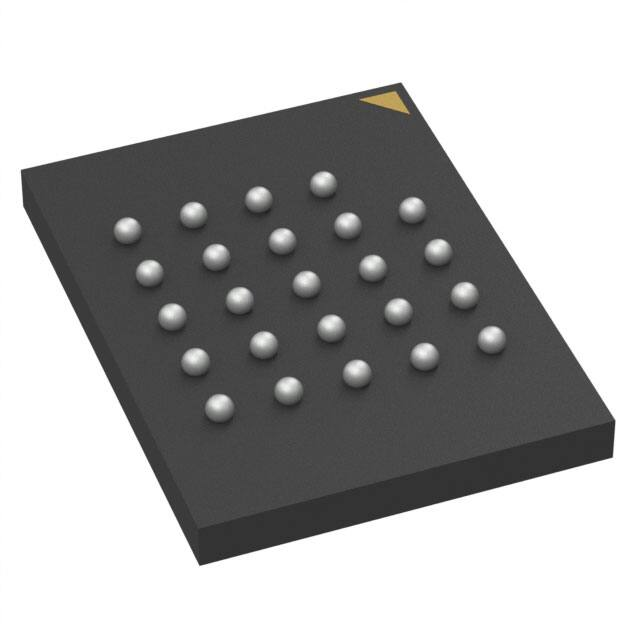


 工商网监
湘ICP备2023018690号
工商网监
湘ICP备2023018690号
