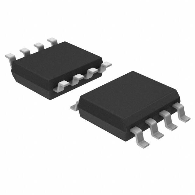
MB3773
Power Supply Monitor with
Watch-Dog Timer
Description
MB3773 generates the reset signal to protect an arbitrary system when the power-supply voltage momentarily is intercepted or
decreased. It is IC for the power-supply voltage watch and “Power on reset” is generated at the normal return of the power supply.
MB3773 sends the microprocessor the reset signal when decreasing more than the voltage, which the power supply of the system
specified, and the computer data is protected from an accidental deletion.
In addition, the watch-dog timer for the operation diagnosis of the system is built into, and various microprocessor systems can provide
the fail-safe function. If MB3773 does not receive the clock pulse from the processor for a specified period, MB3773 generates the
reset signal.
Features
■
Precision voltage detection (VS = 4.2 V ± 2.5%)
■
Detection threshold voltage has hysteresis function
■
Low voltage output for reset signal (VCC = 0.8 V Typ)
■
Precision reference voltage output (VR = 1.245 V ± 1.5%)
■
With built-in watch-dog timer of edge trigger input.
■
External parts are few.(1 piece in capacity)
■
The reset signal outputs the positive and negative both theories reason.
■
One type of package (SOP-8pin : 1 type)
Application
■
Industrial Equipment
■
Arcade Amusement etc.
Cypress Semiconductor Corporation
Document Number: 002-08513 Rev. *C
•
198 Champion Court
•
San Jose, CA 95134-1709
•
408-943-2600
Revised June 28, 2017
�MB3773
Contents
Description ............................................................................. 1
Features .................................................................................. 1
Application ............................................................................. 1
Contents ................................................................................. 2
1. Pin Assignment ................................................................. 3
2. Block Diagram ................................................................... 3
3. Functional Descriptions .................................................... 4
4. Operation Sequence .......................................................... 6
5. Absolute Maximum Ratings ............................................ 7
6. Recommended Operating Conditions ............................. 7
7. Electrical Characteristics .................................................. 8
Document Number: 002-08513 Rev. *C
7.1 DC Characteristics ..................................................... 8
7.2 AC Characteristics ...................................................... 9
8. Typical Characteristic Curves ........................................ 10
9. Application Circuit ........................................................... 13
10. Notes on Use .................................................................. 25
11. Ordering Information ..................................................... 25
12. RoHS Compliance Information of Lead (Pb)
Free version ......................................................................... 25
13. Package Dimension ....................................................... 26
Document History ................................................................ 27
Sales, Solutions, and Legal Information ........................... 28
Page 2 of 28
�MB3773
1. Pin Assignment
(TOP VIEW)
CT
1
8
RESET
RESET
2
7
VS
CK
3
6
V REF
GND
4
5
VCC
(SOE008)
2. Block Diagram
VC
5
Reference AMP
≈ 1.24 V
Reference Voltage Generator
≈ 100
≈ 1.2 μA
kΩ
COMP.S
+
VS
≈ 1.24 V
_
COMP.O
+
+
_
_
R
+
6
VREF
4
GND
≈ 10 μA
≈ 10 μA
Q
_
7
S
≈ 40 kΩ
Inhibit
CK
3
P.G
Document Number: 002-08513 Rev. *C
WatchDog
Timer
1
8
CT
RESET
2
RESET
Page 3 of 28
�MB3773
3. Functional Descriptions
Comp.S is comparator including hysteresis. it compare the reference voltage and the voltage of Vs, so that when the voltage of Vs
terminal falls below approximately 1.23 V, reset signal outputs.
Instantaneous breaks or drops in the power can be detected as abnormal conditions by the MB3773 within a 2 μs interval.
However because momentary breaks or drops of this duration do not cause problems in actual systems in some cases, a delayed
trigger function can be created by connecting capacitors to the Vs terminal.
Comp.O is comparator for turning on/off the RESET/RESET outputs and, compare the voltage of the CT terminal and the threshold
voltage. Because the RESET/RESET outputs have built-in pull-up circuit, there is no need to connect to external pull-up resistor when
connected to a high impedance load such as CMOS logic IC.
(It corresponds to 500 kΩ at Vcc = 5 V.) when the voltage of the CK terminal changes from the “high” level into the “Low” level, pulse
generator is sent to the watch-dog timer by generating the pulse momentarily at the time of drop from the threshold level.
When power-supply voltages fall more than detecting voltages, the watch-dog timer becomes an interdiction.
The Reference amplifier is an op-amp to output the reference voltage.
If the comparator is put up outside, two or more power-supply voltage monitor and overvoltage monitor can be done.
If it uses a comparator of the open-collector output, and the output of the comparator is connected with the Vs terminal of MB3773
without the pull-up resistor, it is possible to voltage monitor with reset-hold time.
Document Number: 002-08513 Rev. *C
Page 4 of 28
�MB3773
MB3773 Basic Operation
VCC
VCC
CT
Logic Circuit
TPR (ms) ≈ 1000 · CT (μF)
TWD (ms) ≈ 100 · CT (μF)
TWR (ms) ≈
20 · CT (μF)
RESET
RESET
CK
RESET
RESET
CK
Example : CT = 0.1 μF
TRR (ms) ≈ 100 (ms)
TWD (ms) ≈ 10 (ms)
TWR (ms) ≈ 2 (ms)
GND
VCC
VSH
VSL
0.8 V
CK
TCK
CT
TPR
RESET
(1) (2)
Document Number: 002-08513 Rev. *C
TWD
TWR
(3)(4)(5)
(5)
(6) (7)
TPR
(8)(9)
(10)
(11) (12)
Page 5 of 28
�MB3773
4. Operation Sequence
1. When Vcc rises to about 0.8 V, RESET goes “Low” and RESET goes “High”.
The pull-up current of approximately 1 μA (Vcc = 0.8 V) is output from RESET.
2. When Vcc rises to VSH (≈ 4.3V), the charge with CT starts.
At this time, the output is being reset.
3. When CT begins charging, RESET goes “High” and RESET goes “Low”.
After TPR reset of the output is released.
Reset hold time: TPR (ms) ≈ 1000 × CT (μF)
After releasing reset, the discharge of CT starts, and watch-dog timer operation starts.
TPR is not influenced by the CK input.
4. C changes from the discharge into the charge if the clock (Negative edge) is input to the CK terminal while discharging CT.
5. C changes from the charge into the discharge when the voltage of CT reaches a constant
threshold (≈ 1.4 V).
4 and 5 are repeated while a normal clock is input by the logic system.
6. When the clock is cut off, gets, and the voltage of CT falls on threshold (≈ 0.4 V) of reset on, RESET goes “Low” and RESET goes
“High”.
Discharge time of CT until reset is output: TWD is watch-dog timer monitoring time.
TWD (ms) ≈ 100 × CT (μF)
Because the charging time of CT is added at accurate time from stop of the clock and getting to the output of reset of the clock,
TWD becomes maximum TWD + TWR by minimum TWD.
7. Reset time in operating watch-dog timer: TWR is charging time where the voltage of CT goes up to off
threshold (≈ 1.4 V) for reset.
TWR (ms) ≈ 20 × CT (μF)
Reset of the output is released after CT reaches an off threshold for reset, and CT starts the discharge, after that if the clock is
normally input, operation repeats 4 and 5, when the clock is cut off, operationrepeats 6 and 7.
8. When Vcc falls on VSL (≈ 4.2 V), reset is output. CT is rapidly discharged of at the same time.
9. When Vcc goes up to VSH, the charge with CT is started.
When Vcc is momentarily low,
After falling VSL or less Vcc, the time to going up is the standard value of the Vcc input pulse width in VSH or more.
After the charge of CT is discharged, the charge is started if it is TPI or more.
10.Reset of the output is released after TPR, after Vcc becomes VSH or more, and the watch-dog timer starts. After that, when Vcc
becomes VSL or less, 8 to 10 is repeated.
11.While power supply is off, when Vcc becomes VSL or less, reset is output.
12.The reset output is maintained until Vcc becomes 0.8 V when Vcc falls on 0 V.
Document Number: 002-08513 Rev. *C
Page 6 of 28
�MB3773
5. Absolute Maximum Ratings
Parameter
Rating
Symbol
Unit
Min
Max
VCC
- 0.3
+ 18
V
VS
- 0.3
VCC + 0.3 ( ≤ +18)
V
VCK
- 0.3
+ 18
V
RESET, RESET Supply voltage
VOH
- 0.3
VCC + 0.3 ( ≤ +18)
V
Power dissipation (Ta ≤ +85°C)
PD
—
200
mW
TSTG
- 55
+ 125
°C
Supply voltage
Input voltage
Storage temperature
WARNING: Semiconductor devices can be permanently damaged by application of stress (voltage, current, temperature, etc.) in
excess of absolute maximum ratings. Do not exceed these ratings.
6. Recommended Operating Conditions
Parameter
Symbol
Value
Min
Max
Unit
Supply voltage
VCC
+ 3.5
+ 16
V
RESET, RESET sink current
IOL
0
20
mA
VREF output current
IOUT
- 200
+5
μA
Watch clock setting time
tWD
0.1
1000
ms
CK Rising/falling time
tFC, tRC
—
100
μs
Terminal capacitance
CT
0.001
10
μF
Operating ambient temperature
Ta
- 40
+ 85
°C
WARNING: The recommended operating conditions are required in order to ensure the normal operation of the semiconductor
device.All of the device’s electrical characteristics are warranted when the device is operated within these ranges.
Always use semiconductor devices within their recommended operating condition ranges. Operation outside these
ranges may adversely affect reliability and could result in device failure.
No warranty is made with respect to uses, operating conditions, or combinations not represented on the data sheet.
Users considering application outside the listed conditions are advised to contact their Cypress representatives
beforehand.
Document Number: 002-08513 Rev. *C
Page 7 of 28
�MB3773
7. Electrical Characteristics
7.1 DC Characteristics
(VCC = 5 V, Ta = + 25°C)
Parameter
Supply current
Symbol
ICC
VSL
Detection voltage
VSH
Hysteresis width
VHYS
Reference voltage
VREF
Condition
Value
Min
Typ
Max
—
600
900
VCC
4.10
4.20
4.30
Ta = - 40°C to + 85°C
4.05
4.20
4.35
VCC
4.20
4.30
4.40
Ta = - 40°C to + 85°C
4.15
4.30
4.45
50
100
150
1.227
1.245
1.263
1.215
1.245
1.275
Watch-dog timer operating
VCC
—
Ta = - 40°C to + 85°C
Unit
μA
V
mV
V
Reference voltage change rate
∆VREF1
VCC = 3.5 V to 16 V
—
3
10
mV
Reference voltage output
loading change rate
∆VREF2
IOUT = - 200 μA to + 5 μA
-5
—
+5
mV
Ta = - 40°C to + 85°C
0.8
1.25
2.0
V
IIH
VCK = 5.0 V
—
0
1.0
IIL
VCK = 0.0 V
- 1.0
- 0.1
—
CK threshold voltage
CK input current
CT discharge current
High level output voltage
Output saturation voltage
Output sink current
CT charge current
VTH
μA
ICTD
Watch-dog timer operating
VCT = 1.0 V
7
10
14
VOH1
VS open, IRESET = - 5 μA
4.5
4.9
—
VOH2
VS = 0 V, IRESET = - 5 μA
4.5
4.9
—
VOL1
VS = 0 V, IRESET = 3 mA
—
0.2
0.4
VOL2
VS = 0 V, IRESET = 10 mA
—
0.3
0.5
VOL3
VS open, IRESET = 3 mA
—
0.2
0.4
VOL4
VS open, IRESET = 10 mA
—
0.3
0.5
IOL1
VS = 0 V, VRESET = 1.0 V
20
60
—
IOL2
VS open, VRESET = 1.0 V
20
60
—
ICTU
Power on reset operating
VCT = 1.0 V
0.5
1.2
2.5
μA
μA
V
V
mA
Min supply voltage for RESET
VCCL1
VRESET = 0.4 V,
IRESET = 0.2 mA
—
0.8
1.2
V
Min supply voltage for RESET
VCCL2
VRESET = VCC - 0.1 V,
RL (between pin 2 and GND) = 1 MΩ
—
0.8
1.2
V
Document Number: 002-08513 Rev. *C
Page 8 of 28
�MB3773
7.2 AC Characteristics
Parameter
Symbol
VCC input pulse width
TPI
CK input pulse width
TCKW
Condition
5V
VCC 4 V
CK
or
(VCC = 5 V, Ta = + 25°C)
Value
Unit
Min
Typ
Max
8.0
—
—
μs
3.0
—
—
μs
CK input frequency
TCK
20
—
—
μs
Watch-dog timer watching time
TWD
CT = 0.1 μF
5
10
15
ms
Watch-dog timer reset time
TWR
CT = 0.1 μF
1
2
3
ms
Rising reset hold time
TPR
CT = 0.1 μF, VCC
50
100
150
ms
TPD1
RESET, RL = 2.2 kΩ,
CL = 100 pF
—
2
10
TPD2
RESET, RL = 2.2 kΩ,
CL = 100 pF
—
3
10
tR
RL = 2.2 kΩ,
CL = 100 pF
—
1.0
1.5
tF
RL = 2.2 kΩ,
CL = 100 pF
—
Output propagation
delay time from VCC
Output rising time*
Output falling time*
—
μs
μs
0.1
0.5
* : Output rising/falling time are measured at 10 % to 90 % of voltage.
Document Number: 002-08513 Rev. *C
Page 9 of 28
�MB3773
8. Typical Characteristic Curves
Supply current vs. Supply voltage
6.0
Ta = + 85 °C
Ta = + 25 °C
0.65
Ta = − 40 °C
0.55
CT = 0.1 μF
0.45
Ta = − 40 °C
0.35
Ta = + 25 °C
Ta = + 85 °C
0.25
0.15
0
2.0
4.0
6.0
Output voltage VRESET (V)
Supply current ICC (mA)
0.75
Output voltage vs. Supply voltage
(RESET terminal)
Pull up 2.2 kΩ
5.0
Ta = − 40 °C, + 25 °C, + 85 °C
4.0
3.0
2.0
1.0
0
8.0 10.0 12.0 14.0 16.0 18.0 20.0
1.0
(RESET terminal)
6.0
4.0
5.0
6.0
7.0
4.50
Pull up 2.2 kΩ
5.0
4.0
3.0
2.0
Ta = + 85 °C
Ta = + 25 °C
Ta = − 40 °C
1.0
0
1.0
2.0
3.0
4.0
5.0
6.0
7.0
Detection voltage VSH, VSL (V)
Output voltage VRESET (V)
3.0
Detection voltage (VSH, VSL) vs.
Operating ambient temperature
(RESET, RESET terminal)
Output voltage vs. Supply voltage
4.44
VSH
4.30
VSL
4.20
4.10
4.00
Supply voltage VCC (V)
−40
Ta = − 40 °C
CT = 0.1μF
400
300
Ta = + 25 °C
Ta = + 85 °C
200
100
0
2.0
4.0
6.0 8.0 10.0 12.0 14.0 16.0 18.0
Output sink current IOL2 (mA)
0
+20
+40
+60
+80 +100
Output saturation voltage
vs. Output sink current
(RESET terminal)
Output saturation voltage VOL2 (mV)
(RESET terminal)
−20
Operating ambient temperature Ta (°C)
Output saturation voltage
vs. Output sink current
Output saturation voltage VOL2 (mV)
2.0
Supply voltage VCC (V)
Supply voltage VCC (V)
500
CT = 0.1μF
Ta = −40 °C
400
300
Ta = +25 °C
Ta = +85 °C
200
100
0
2.0 4.0
6.0
8.0 10.0 12.0 14.0 16.0 18.0
Output sink current IOL8 (mA)
(Continued)
Document Number: 002-08513 Rev. *C
Page 10 of 28
�MB3773
High level output voltage
vs. High level output current
High level output voltage VOH2 (V)
(RESET terminal)
5.0
CT = 0.1 μF
Ta = +25 °C
Ta = −40 °C
4.5
4.0
Ta = +85 °C
−5
0
−10
−15
High level output voltage VOH8 (V)
High level output voltage
vs. High level output current
(RESET terminal)
5.0
CT = 0.1 μF
Ta = −40 °C
4.5
4.0
Ta = +25 °C
Ta = +85 °C
−5
0
−10
−15
High level output current IOH8 (μA)
High level output current IOH2 (μA)
Reference voltage
vs. Reference current
Reference voltage
vs. Supply voltage
Ta = +25 °C
1.244
Ta = +85 °C
1.242
Ta = −40 °C
1.240
CT = 0.1 μF
1.238
1.236
1.234
0
1.255
Reference voltage VREF (V)
Reference voltage VREF (V)
1.246
3.0 5.0 7.0 9.0 11.0 13.0 15.0 17.0 19.0 21.0
1.250
Ta = +25 °C
1.245
Ta = +85 °C
Ta = −40 °C
1.240
−40
0
Supply voltage VCC (V)
Reference voltage vs.
Operating ambient temperature
−80
−120
−160
−200
Reference current IREF (μA)
−240
Rising reset hold time vs.
Operating ambient temperature
1.27
160
Rising reset hold time TPR (ms)
Reference voltage VREF (V)
CT = 0.1 μF
1.26
1.25
1.24
1.23
1.22
1.21
−40 −20
0
+20 +40 +60 +80 +100
Operating ambient temperature Ta (°C)
VCC = 5 V
CT = 0.1 μF
140
120
100
80
60
40
0
−40 −20
0
+20 +40 +60 +80 +100
Operating ambient temperature Ta (°C)
(Continued)
Document Number: 002-08513 Rev. *C
Page 11 of 28
�MB3773
(Continued)
Reset time vs.
Operating ambient temperature
Watch-dog timer watching time vs.
Operating ambient temperature
(At watch-dog timer)
2
1
0
−40
−20
0
+20
+40 +60
12
10
8
6
4
0
+80 +100
Operating ambient temperature Ta (°C)
Watch-dog timer watching time
vs.
CT terminal capacitance
VCC = 5 V
CT = 0.1 μF
14
Watch-dog timer
watching time TWD (ms)
Reset time TWR (ms)
16
VCC = 5 V
CT = 0.1 μF
3
−40
−20
0
+20 +40
+60
+80 +100
Operating ambient temperature Ta (°C)
Reset time vs.
CT terminal capacitance
Rising reset hold time vs.
CT terminal capacitance
(at watch-dog timer)
10 6
10 6
10 4
10 3
10 2
Ta = −40 °C
Ta =
+25 °C, +85 °C
10 1
10 0
10 −1
Reset time TWR (ms)
Watch-dog timer
watching time TWD (ms)
10 5
10 1
Ta = +25 °C,
+85 °C
10 0
10 −1
Ta =
−40 °C
10 −2
10 −2
10 −3
10 −3 10 −2 10 −1 10 0 10 1 10 2
CT terminal capacitance CT (μF)
Document Number: 002-08513 Rev. *C
10 −3
Rising reset hold time TPR (ms)
10 2
10 −3 10 −2 10 −1 10 0 10 1 10 2
CT terminal capacitance CT (μF)
10 5
10 4
10 3
10 2
10 1
Ta = −40 °C
Ta = +25 °C, +85 °C
10 0
10 −1
10 −2
10 −3
10 −3 10 −2 10 −1 10 0 10 1 10 2
CT terminal capacitance CT (μF)
Page 12 of 28
�MB3773
9. Application Circuit
EXAMPLE 1: Monitoring 5V Supply Voltage and Watch-dog Timer
VCC (5V)
MB3773
8
7
6
5
1
2
3
4
CT
Logic circuit
RESET
RESET
CK
GND
Notes :
• Supply voltage is monitored using VS.
• Detection voltage are VSH and VSL.
EXAMPLE 2: 5V Supply Voltage Monitoring (external fine-tuning type)
VCC (5V)
MB3773
1
2
3
4
CT
Logic circuit
R1
8
7
6
5
R2
RESET
RESET
CK
GND
Notes :
• Vs detection voltage can be adjusted externally.
• Based on selecting R1 and R2 values that are sufficiently lower than the resistance of the IC’s internal voltage
divider, the detection voltage can be set according to the resistance ratio of R1 and R2 (Refer to the table
below.)
R1 (kΩ)
R2 (kΩ)
Detection voltage: VSL (V)
Detection voltage: VSH (V)
10
3.9
4.4
4.5
9.1
3.9
4.1
4.2
Document Number: 002-08513 Rev. *C
Page 13 of 28
�MB3773
EXAMPLE 3: With Forced Reset (with reset hold)
(a)
VCC
MB3773
CT
1
2
3
4
Logic circuit
8
7
6
5
SW
RESET
RESET
CK
GND
Note : Grounding pin 7 at the time of SW ON sets RESET (pin 8) to Low and RESET (pin 2) to High.
(b)
VCC
MB3773
Cr
1
2
3
4
8
7
6
5
Logic circuit
Tr
10 kΩ
10 kΩ
RESET
RESET
CK
GND
RESIN
Note : Feeding the signal to terminal RESIN and turning on Tr sets the RESET terminal to Low and the
RESET terminal to High.
Document Number: 002-08513 Rev. *C
Page 14 of 28
�MB3773
EXAMPLE 4: Monitoring Two Supply Voltages (with hysteresis, reset output and NMI)
VCC2(12
VCC1 (5
Logic circuit
MB3773
CT
1
2
3
4
RESET
8
7
6
5
RESET
CK
30 kΩ
R3
180 kΩ
10 kΩ
R6
R4
NMI or port
GND
+
+
_
_
Comp. 1
1.2 kΩ
R1
5.1 kΩ
R2
Comp. 2
4.7 kΩ
R5
Example : Comp. 1, Comp. 2
: MB4204, MB47393
Notes :
• The 5 V supply voltage is monitored by the MB3773.
• The 12 V supply voltage is monitored by the external circuit. Its output is connected to the NMI terminal and, when
voltage drops, Comp. 2 interrupts the logic circuit.
• Use VCC1 ( = 5 V) to power the comparators (Comp. 1 and Comp. 2) in the external circuit shown above.
• The detection voltage of the VCC2 ( = 12 V) supply voltage is approximately 9.2 V/9.4 V and has a hysteresis width
of approximately 0.2 V.
VCC2 detection voltage and hysteresis width can be found using the following formulas:
→ Detection voltage
→ Hysteresis width
V2H =
R3 + (R4 // R5)
× VREF
R4 // R5
(Approximately 9.4 V in the above illustration)
V2L =
R3 + R5
× VREF
R5
(Approximately 9.2 V in the above illustration)
VHYS = V2H − V2L
Document Number: 002-08513 Rev. *C
Page 15 of 28
�MB3773
EXAMPLE 5: Monitoring Two Supply Voltages (with hysteresis and reset output)
VCC2 (12
VCC1 (5 V)
20 kΩ
R6
MB3773
CT
1
2
3
4
8
7
6
5
30 kΩ
R3
Diode
Logic circuit
RESET
RESET
CK
GND
180 kΩ
R4
+
_
Comp. 1
1.2 kΩ
R1
5.1 kΩ
R2
+
_
Comp. 2
4.7 kΩ
R5
Example : Comp. 1, Comp. 2
: MB4204, MB47393
Notes :
• When either 5 V or 12 V supply voltage decreases below its detection voltage (VSL), the MB3773 RESET terminal
is set to High and the MB3773 RESET terminal is set to Low.
• Use VCC1 ( = 5 V) to power the comparators (Comp. 1 and Comp. 2) in the external circuit shown above.
• The detection voltage of the VCC2 ( = 12 V) supply voltage is approximately 9.2 V/9.4 V and has a hysteresis width
of approximately 0.2 V. For the formulas for finding hysteresis width and detection voltage, refer to section 4.
Document Number: 002-08513 Rev. *C
Page 16 of 28
�MB3773
EXAMPLE 6: Monitoring Low voltage and Overvoltage Monitoring (with hysteresis)
VCC (5
20 kΩ
R6
MB3773
CT
1
2
3
4
8
7
6
5
RESET
RESET
CK
GND
Diode
30 kΩ
R3
Logic circuit
180 kΩ
R4
+
_
_
5.6 kΩ
R6
+
Comp. 1
1.2 kΩ
R1
Comp. 2
4.7 kΩ
R5
Example : Comp. 1, Comp. 2
: MB4204, MB47393
RESET
0
V1L V1H
V2L V2H
VCC
Notes :
• Comp. 1 and Comp. 2 are used to monitor for overvoltage while the MB3773 is used to monitor for low voltage.
Detection voltages V1L/V1H at the time of low voltage are approximately 4.2 V/4.3 V. Detection voltages V2L/V2H at
the time of overvoltage are approximately 6.0 V/6.1 V.For the formulas for finding hysteresis width and detection
voltage, see EXAMPLE 4.
• Use VCC ( = 5 V) to power the comparators (Comp. 1 and Comp. 2) in the external circuit shown above.
Document Number: 002-08513 Rev. *C
Page 17 of 28
�MB3773
EXAMPLE 7: Monitoring Supply Voltage Using Delayed Trigger
VCC
5V
VCC
4V
MB3773
CT
1
2
3
4
8
7
6
5
Logic circuit
C1
RESET
RESET
CK
GND
Note : Adding voltage such as shown in the figure to VCC increases the minimum input pulse
width by 50 μs (C1 = 1000 pF).
Document Number: 002-08513 Rev. *C
Page 18 of 28
�MB3773
EXAMPLE 8: Stopping Watch-dog Timer (Monitoring only supply voltage)
These are example application circuits in which the MB3773 monitors supply voltage alone without resetting the microprocessor even if the latter, used in standby mode, stops sending the clock pulse to the MB3773.
• The watch-dog timer is inhibited by clamping the CT terminal voltage to VREF.
The supply voltage is constantly monitored even while the watch-dog timer is inhibited.
For this reason, a reset signal is output at the occurrence of either instantaneous disruption or a sudden drop to low voltage.
Note that in application examples (a) and (b), the hold signal is inactive when the watch-dog timer is inhibited at the time of
resetting.
If the hold signal is active when tie microprocessor is reset, the solution is to add a gate, as in examples (c) and (d).
(a) Using NPN transistor
VCC(5 V)
MB3773
1
2
3
4
Logic circuit
RESET
RESET
CK
HALT
8
7
6
5
GND
R2=1 kΩ
R1=1 MΩ
CT
(b) Using PNP transistor
VCC (5 V)
MB3773
Logic circuit
1
8
2
7
3
6
4
5
RESET
RESET
CK
HALT
GND
R2=1 kΩ
R1=51
CT
(Continued)
Document Number: 002-08513 Rev. *C
Page 19 of 28
�MB3773
(Continued)
(c) Using NPN transistor
VCC (5 V)
MB3773
1
2
3
4
Logic circuit
8
7
6
5
R1=1 MΩ
RESET
RESET
CK
HALT
GND
R2=1 kΩ
CT
(d) Using PNP transistor
VCC (5 V)
MB3773
1
2
3
4
Logic circuit
8
7
6
5
R1=51 kΩ
RESET
RESET
CK
HALT
GND
R2=1 kΩ
CT
Document Number: 002-08513 Rev. *C
Page 20 of 28
�MB3773
EXAMPLE 9: Reducing Reset Hold Time
VCC ( = 5 V)
VCC( = 5 V)
MB3773
CT
1
2
3
4
8
7
6
5
MB3773
Logic circuit
RESET
RESET
CK
GND
CT
(a) TPR reduction method
1
2
3
4
8
7
6
5
Logic circuit
RESET
RESET
CK
GND
(b) Standard usage
Notes :
• RESET is the only output that can be used.
• Standard TPR, TWD and TWR value can be found using the following formulas.
Formulas:TPR (ms) ≈ 100 × CT (μF)
TWD (ms) ≈ 100 × CT (μF)
TWR (ms) ≈ 16 × CT (μF)
• The above formulas become standard values in determining TPR, TWD and TWR.
Reset hold time is compared below between the reduction circuit and the standard circuit.
CT = 0.1 μF
TPR reduction circuit
Standard circuit
TPR ≈
10 ms
100 ms
TWD ≈
10 ms
10 ms
TWR ≈
1.6 ms
2.0 ms
Document Number: 002-08513 Rev. *C
Page 21 of 28
�MB3773
EXAMPLE 10: Circuit for Monitoring Multiple Microprocessor
FF1
S
D1 Q1
FF2
S
D2 Q2
VCC ( = 5
FF3
S
D3 Q3
CK Q1
CK2 Q2
CK Q3
R
R
R
R2
*
*
R1
*
RESET
RESET
RESET
RESET
RESET
RESET
CK
CK
CK
GND
GND
GND
CT
*: Microprocessor
1
2
8
7
3
4
6
5
MB3773
Figure 1
Notes :
•
connects from FF1 and FF2 outputs Q1 and Q2 to the NOR input.
• Depending on timing, these connections may not be necessary.
• Example : R1 = R2 = 2.2 kΩ
CT = 0.1 μF
CK1
Q1
CK2
Q2
CK3
Q3
NOR
Output
Document Number: 002-08513 Rev. *C
Figure 2
Page 22 of 28
�MB3773
Description of Application Circuits
Using one MB3773, this application circuit monitors multiple microprocessor in one system. Signals from each microprocessor are
sent to FF1, FF2 and FF3 clock inputs. Figure 2 shows these timings. Each flip-flop operates using signals sent from microprocessor
as its clock pulse. When even one signal stops, the relevant receiving flip-flop stops operating. As a result, cyclical pulses are not
generated at output Q3. Since the clock pulse stops arriving at the CK terminal of the MB3773, the MB3773 generates a reset signal.
Note that output Q3 frequency f will be in the following range, where the clock frequencies of CK1, CK2 and CK3 are f1, f2 and f3
respectively.
1 1 1 1 1
---- ≤ --- ≤ --- + ---- + ---f0 f f1 f2 f3
where f0 is the lowest frequency among f1, f2 and f3.
Document Number: 002-08513 Rev. *C
Page 23 of 28
�MB3773
EXAMPLE 11: Circuit for Limiting Upper Clock Input Frequency
VCC (5 V)
R2
1
2
3
4
CT
8
7
6
5
RESET
RESET
R1=10 kΩ
CK
GND
Tr1
C2
Notes :
• This is an example application to limit upper frequency fH of clock pulses sent from the microprocessor.
If the CK cycle sent from the microprocessor exceeds fH, the circuit generates a reset signal.
(The lower frequency has already been set using CT.)
• When a clock pulse such as shown below is sent to terminal CK, a short T2 prevents C2 voltage from reaching the
CK input threshold level ( := 1.25 V), and will cause a reset signal to be output.
The T1 value can be found using the following formula :
T1 ≈ 0.3 C2R2
where VCC = 5 V, T3 ≥ 3.0 μs, T2 ≥ 20 μs
T2
CK waveform
T3
C2 voltage
T
Example : Setting C and R allow the upper T1 value to be set (Refer to the table below).
C
R
T1
0.01 μF
10 kΩ
30 μs
0.1 μF
10 kΩ
300 μs
Document Number: 002-08513 Rev. *C
Page 24 of 28
�MB3773
10. Notes on Use
■
■
Take account of common impedance when designing the earth line on a printed wiring board.
Take measures against static electricity.
For semiconductors, use antistatic or conductive containers.
❐ When storing or carrying a printed circuit board after chip mounting, put it in a conductive bag or container.
❐ The work table, tools and measuring instruments must be grounded.
❐ The worker must put on a grounding device containing 250 kΩ to 1 MΩ resistors in series.
❐
■
Do not apply a negative voltage
Applying a negative voltage of −0.3 V or less to an LSI may generate a parasitic transistor, resulting in
malfunction.
❐
11. Ordering Information
Part number
MB3773PF-❏❏❏E1
Package
Remarks
8-pin plastic SOP
(SOE008)
–
12. RoHS Compliance Information of Lead (Pb) Free version
The LSI products of Cypress with “E1” are compliant with RoHS Directive , and has observed the standard of lead, cadmium, mercury,
Hexavalent chromium, polybrominated biphenyls (PBB) , and polybrominated diphenyl ethers (PBDE) .
The product that conforms to this standard is added “E1” at the end of the part number.
Document Number: 002-08513 Rev. *C
Page 25 of 28
�MB3773
13. Package Dimension
b
0.39
0.47
0.55
L
0.45
0.60
0.75
�
�
1
,
3
�
$
�
1
'
((
+7
7$
�&
�
7,
1'
(1
,
6�
($
5(
35
�$
7
�
2;
1(
�'
6
1
,
�
,
7(
�
,
�
+
)
/7
�1
�
�
/
,
$+
17
2,
,:
7
�
3'
2(
�7
6
$
,
�
&
(
52
/
8�
7(
$%
(7
�
)6
�8
5
(0
)�
05
(
$,
+,
)
&7
�1
6
,
(
+'
7,
�
��
�
�
�
�
2 �
756
�21
(
�2
1'
,
$17
/$$
3�
'5
�,
*
/8
1�
*
,(
,
7
+)
$7
1
(�
2
6*&
1�
�
(,
(
+'*
78$
�/.
0
&
2;&
5($
3
)<
��
�'
1
(
&2:
1%2
$ '
�
7(�
6*<
,
$7
'.
,
9
�&
/
$
$$&
&3�
,
�1
7
(
5+2
�
(77
9�1
�1(
(
20
+�
77
(
�1&
6
,
$21
�3$
'
+
�
�
(7
1
16(
,
�
)(/
(:$
'20
�/
6
5
�(
,
(
�
�
+
+
�
$77
��
��
�
�
�
��
�
�
�
�
�
�
�
��
�
002-15857 Rev. **
11. JEDEC SPECIFICATION NO. REF : N/A
b
A'
Page 26 of 28
Document Number: 002-08513 Rev. *C
1
2
,
6
1
(
�
/( 7
%0 2
,
$'
2
� )
:�
2E
� �
(
/� +
/( 7
$+ �
7
��
)
�
1
) 2
22 �
6
,� 8
6
6 ,
86 '
5( $
7& 5
2; �
5( 5
3� (
1
�,
:
5
� 2
$/
/
%$ �
7
02
(
$7
+
7
'�
�
�P
1
(
+P 2
7� '
�
�
�
��
1
(
(
�2
'�
7
8(,
$
7&
/%,
�
'
&/
2
1/1
,$ /
2
�
(
+&�
7
%
26/
��
7
1�
1$2
�2,
6
51
(,
6(�
28
7<
'5$$
0
�
�70�
E
2�5
�
�
50$
1
8
%
2300
,�
5,
6
;
$
1$$'
(% �
0
0
(
0$
�+
7
,'
' $7
�
��
��
��
�
�
��
��
�
�
L 2
�
0.13
DETAIL A
SIDE VIEW
�
c
P
P
�
�
�
�
�
�
1
(
(
:
7
(
%
�
'
$
(
/
�
(
+
7
�
)
2
�
1
2
,
7
&
(
6
�
7
$
/
)�
�
3
(,
+7
7�
'
�$
2
7(
�/
<
�
/(
3+
37
$�
�0
1
2
25
,)
6
�
1P
(P
0�
,�
'
�
��
(
�
+2
77
�
��
�
�
�
�
1.25 REF
0.25 BSC
'
(
,
)
,
&
(
3
6
�
(
+
7
�
5
2
)
�
6
1
2
,
7
,
6
2
3
�
/
$
1
,
0
5
(
7
�
)
2
�
5
(
%
0
8
1
��
0
8+
07
,*
;
1
$(
/
0�
�(
(
+*
7$
�.
6
&
,
�
$
�
13
��
�
�
�
�
�
�
�
L 1
�
+
�
0
8
7
$
'
�
7
$
�
'
(
1
,
0
5
(
7
(
'
�
(
%
�
2
7
�
%
�
�
$
�
6
0
8
7
$
'
�
�
�
0.20
0°
L2
DETAIL A
�
8°
ș
�
5.30 BSC
�
<
*'
12
,
�
%
'
0
�
&
8,
2
77�/7
76+&6
1
$
226,
/
�3
%0$7
�
(5/8(
�
)
%+
*('
��
�7
$7/
+�
.82
6)
2
&�
0$2
$(
�
3 �
)/0
+
)
�7
2'
�2
(
+�
7�
( 7
$
7$9(
7
�'
,/2
�6
1
%
$(85�
+1/('
7,&71
1$
�0;,
5
�
(5(�3
/(�'2
/7