MB39A130A
MB39A130A 1ch DC/DC Buck Converter
IC with Synchronous Rectification
Description
MB39A130A is a 1ch DC/DC Buck converter equipped with a bottom detection comparator and N-ch/N-ch synchronous rectification.
It supports low on-duty operation to allow stable output of low voltages when there is a large difference between input and output
voltages. MB39A130A realizes ultra-rapid response and high efficiency with built-in enhanced protection features.
Features
•
•
•
•
•
•
•
•
•
•
•
•
•
•
•
•
•
Power conversion efficiency
:96 % (Max.)
Adjustable frequency setting by an external resistor
:100 kHz to 600 kHz
High accuracy reference voltage
: ±1.0%
Output voltage setting range
:0.7 V to 5 V or fixed to 1.2 V/2.5 V
Adjustable output voltages setting by the external control
Input voltage range (VIN)
:4.5 V to 25 V
Inductor saturation detection function which can be set optional
Built-in over voltage protection function
Built-in under voltage protection function
Built-in over current protection function
Built-in Power-Good detection function
Built-in over temperature protection function
Built-in soft-start circuit without load dependence
Built-in discharge control circuit
Built-in synchronous rectification type output driver for N-ch MOS FET
Standby current
: 0 [µA] (Typ.)
Small package
: TSSOP-24 (4.4 × 6.5 [mm])
Applications
•
•
•
•
•
Digital TV
Photocopiers
STB
BD, DVD players/recorders
Projectors
Various other advanced devices
Cypress Semiconductor Corporation
Document Number: 002-08423 Rev. *C
•
198 Champion Court
•
San Jose, CA 95134-1709
•
408-943-2600
Revised June 13, 2017
�MB39A130A
Contents
Description ........................................................................ 1
Features ............................................................................. 1
Applications ...................................................................... 1
1. Pin Assignment ........................................................... 3
2. Pin Descriptions .......................................................... 4
3. Block Diagram ............................................................. 5
4. Absolute Maximum Ratings ....................................... 6
5. Recommended Operating Conditions ....................... 7
6. Electrical Characteristics ............................................ 8
7. Diagram of Feedback Voltage Measurement Circuit
..................................................................................... 12
8. Typical Characteristics ............................................. 13
9. Function ..................................................................... 17
9.1 Reference Voltage Block (REF) ......................... 18
9.2 Under Voltage Lockout Protection Circuit Block (UVLO)
............................................................................... 18
9.3 Soft-start Block (Soft-Start) ................................. 18
9.4 Discharge Block (Discharge) .............................. 18
9.5 ON/OFF Time Generator Block (tON Generator)
............................................................................... 19
9.6 Output Voltage Setting Block (VO REFIN Control, Error
Comp.) ................................................................. 20
9.7 Current Detection Block (Current Sense) ........... 21
9.8 Over Current Detection Block (ILIM Comp.) ....... 21
Document Number: 002-08423 Rev. *C
9.9 Inductor Saturation Detection Block (LSAT Comp.)
............................................................................... 22
9.10 Over-voltage Protection Circuit Block (OVP Comp.)
............................................................................... 23
9.11 Under-voltage Protection Circuit Block (UVP Comp.)
............................................................................... 24
9.12 Power-Good Detection Circuit Block (PGOOD Comp.)
.............................................................................. 24
9.13 Output Block (Drv-1, Drv-2) .............................. 25
9.14 Control Block (CTL) .......................................... 25
9.15 Bias Voltage Block (VB Reg.) ........................... 25
9.16 Over temperature Protection Circuit Block (OTP)
............................................................................... 25
10. Protection Function Table ...................................... 26
11. I/O Pin Equivalent Circuit Diagram ........................ 27
12. Example Application Circuit ................................... 30
13. Parts List .................................................................. 31
14. Application Note ...................................................... 32
15. Reference Data ........................................................ 53
16. Usage Precaution .................................................... 57
17. Ordering Information ............................................... 57
18. RoHS Compliance Information ............................... 57
19. Package Dimensions ............................................... 58
Sales, Solutions, and Legal Information ...................... 60
Page 2 of 60
�MB39A130A
1. Pin Assignment
(TOP VIEW)
GND : 1
24 : FB
REFIN : 2
23 : VO
VREF : 3
22 : RT
CS : 4
21 : CB
COVP : 5
20 : OUT-1
CUVP : 6
19 : LX
TSSOP-24
PGOOD : 7
18 : VBIN
CTL : 8
17 : VCC
LSAT : 9
16 : VB
ILIM : 10
15 : OUT-2
+INC : 11
14 : PGND
−INC : 12
13 : FSW
(STD024)
Document Number: 002-08423 Rev. *C
Page 3 of 60
�MB39A130A
2. Pin Descriptions
Pin No.
Pin Name
I/O
Description
1
GND
-
Ground pin.
2
REFIN
I
Reference voltage input pin for Error Comp.
3
VREF
O
Reference voltage output pin.
4
CS
I
Soft-start time setting capacitor connection pin.
5
COVP
-
Detection time setting capacitor connection pin for OVP function.
The OVP function can be disabled by a short circuit with GND pin.
6
CUVP
-
Detection time setting capacitor connection pin for UVP function.
The UVP function can be disabled by a short circuit with GND pin.
7
PGOOD
O
Power-Good detection circuit output pin. (Open-drain output)
8
CTL
I
Power supply control pin.
IC changes to standby state when CTL is set to “L” level.
9
LSAT
I
Inductor oversaturation detection level setting voltage input pin.
10
ILIM
I
Over current detection level setting voltage input pin.
11
+INC
I
Current detection block (Current Sense) input pin.
12
-INC
I
Current detection block (Current Sense) input pin.
13
FSW
I
Preset value switching pin for operating frequency.
14
PGND
-
Ground pin for output circuit.
15
OUT-2
O
Output pin for external low-side FET gate drive.
16
VB
O
Bias output pin for output circuit.
17
VCC
-
Power supply pin.
18
VBIN
I
Bias voltage external input pin for output circuit and control circuit.
19
LX
-
Inductor and external high-side FET source and external low-side FET drain connection pin.
20
OUT-1
O
Output pin for external high-side FET gate drive.
21
CB
-
Connection pin for boot strap capacitor.
It connects a capacitor between CB and LX pins.
22
RT
-
Connection pin for tON time setting resistor.
23
VO
I
Input pin for DC/DC output voltage.
24
FB
I
Feedback pin for DC/DC output voltage.
Document Number: 002-08423 Rev. *C
Page 4 of 60
�MB39A130A
3. Block Diagram
FSW
RT
22
VCC
13
17
VBIN
18
CTL uvp otp
VB
VB Reg.
VREF
5 μA
CTL,
uvlo
CS
16
(5 V)
tON
Generator
ON/OFF
(4.5 V)
CB
4
21
VO
OUT-1
23
Drv-1
LX
Drive Logic
VO
REFIN
Control
FB
20
19
OUT-2
24
Drv-2
15
2
REFIN
INTREF
PGND
+INC
-INC
14
11
12
Current
Sense
LSAT
9
10 μA
9:1
ILIM
VB
9:1
H:UVLO
release
10
VB
UVLO
5 μA
5
VREF
UVLO
COVP
S Q
R
VB
INTREF x 1.15 V
CUVP
PGOOD
7
5 μA
6
S Q
R
INTREF x 0.7 V
VCC
ON/OFF
bias
INTREF x 0.9 V
CTL
8
(2.5 V)
3
VREF
Document Number: 002-08423 Rev. *C
1
GND
Page 5 of 60
�MB39A130A
4. Absolute Maximum Ratings
Parameter
Symbol
Condition
VCC
−
−
−
−
Power supply voltage
CB pin input voltage
Voltage between CB and LX
VCB
VCBLX
Bias external input voltage
VBIN
Control input voltage
VI
CTL pin
VI
FB, VO, REFIN, FSW pins
−
−
−
−
−
V+INC
V-INC
Input voltage
VILIM
VLSAT
PGOOD pin voltage
VPG
Output current
IOUT
Power dissipation
Storage temperature
PD
TSTG
DC
Ta ≤ + 25°C
−
Rating
Unit
Min
Max
−
−
−
−
−
−
−
−
−
−
−
−
−
27
V
32
V
7
V
7
V
27
V
VB + 0.3
V
27
V
27
V
VB + 0.3
V
VB + 0.3
V
7
V
60
mA
1315
mW
+125
°C
-55
WARNING: Semiconductor devices can be permanently damaged by application of stress (voltage, current,
temperature, etc.) in excess of absolute maximum ratings. Do not exceed these ratings.
Document Number: 002-08423 Rev. *C
Page 6 of 60
�MB39A130A
5. Recommended Operating Conditions
Parameter
Power supply voltage
Symbol
Condition
VCC
−
−
−
−
CB pin input voltage
VCB
Reference voltage output current
IREF
Bias output current
IVB
CTL pin input voltage
VI
CTL pin
VI
FB, VO, REFIN, FSW pins
V+INC
V-INC
Input voltage
VILIM
VLSAT
PGOOD pin output voltage
VPG
PGOOD pin output current
IPG
Peak output current
IOUT
Operation frequency range
fOSC
Timing resistor
RT
Current detection resistor
RS
Soft start capacitor
CS
CB pin capacitor
CCB
Reference voltage output capacitor
CREF
Bias voltage output capacitor
CVB
Operating ambient temperature
Ta
Value
Min
Typ
Max
4.5
25.0
0
−
−
−
−
−
−
−
−
−
−
−
−
-1200
−
-100
-1
0
−
−
−
−
−
−
Duty≤5%
(t = 1/fOSC × Duty)
−
−
−
−
−
−
−
−
0
-0.3
-0.3
0
0
Unit
V
30
V
0
µA
−
mA
25
V
VB
V
+ 2.9
V
+ 25
V
VB
V
VB
V
5.5
V
4
mA
−
+ 1200
mA
100
450
780
kHz
−
−
−
−
−
−
43
kΩ
0.1
−
−
−
−
0.01
1.0
µF
2.2
10
µF
+ 25
+ 85
°C
0
-30
10
0.018
mΩ
µF
µF
WARNING: The recommended operating conditions are required in order to ensure the normal operation of
the semiconductor device. All of the device's electrical characteristics are warranted when the
device is operated within these ranges.
Always use semiconductor devices within their recommended operating condition ranges.
Operation outside these ranges may adversely affect reliability and could result in device failure.
No warranty is made with respect to uses, operating conditions, or combinations not represented
on the data sheet. Users considering application outside the listed conditions are advised to contact
their representatives beforehand.
Document Number: 002-08423 Rev. *C
Page 7 of 60
�MB39A130A
6. Electrical Characteristics
(Ta = +25°C, VCC pin = 15 V, CTL pin = 5 V, VREF pin = 0 mA)
Parameter
Reference Voltage Block [REF]
Bias Voltage
Block
[VB Reg.]
−
Value
Unit
Min
Typ
Max
2.463
2.500
2.537
V
−
1
10
mV
-20
-10
-5
mA
4.9
5.0
5.1
V
VREF
3
Load
3
VREF pin = 0 µA to -100 µA
Short-circuit output current
IOS
3
VREF pin = 0 V
Output voltage
VB
16
VTLH
18
VBIN pin
4.3
4.5
4.7
V
VTHL
18
VBIN pin
4.1
4.3
4.5
V
Inside/Outside switching
threshold
Hysteresis width
Threshold voltage
−
RSW
18
VBIN pin = 5 V
−
4*
−
Ω
VTLH
16
VB pin
3.8
4.0
4.2
V
VTHL
16
VB pin
3.1
3.3
3.5
V
−
V
1
VH
16
VB pin
−
0.7*1
VTLH
3
VREF pin
1.8
2.0
2.2
V
VTHL
3
VREF pin
1.6
1.8
2.0
V
−
0.2*1
−
V
-6.3
-4.5
-3.1
µA
Hysteresis width
VH
3
VREF pin
Charge current
ICS
4
CTL pin = 5 V, CS pin = 0 V
Electrical discharge
resistance
RD
23
CTL pin = 0 V,
VO pin ≥ 0.3 V
−
16*1
−
Ω
Discharge end voltage
VO
23
CTL pin = 0 V
0.3*1
−
V
ON time
tON
20
RT pin = 43 kΩ,
FSW pin = GND,
VCC pin = 15 V,
VO pin = 1.5 V
−
246
280
314
ns
20
RT pin = GND,
FSW pin = VREF pin,
VCC pin = 15 V,
VO pin = 1.5 V
272
390
508
ns
tON_3
20
RT pin = GND,
FSW pin = VB pin,
VCC pin = 15 V,
VO pin = 1.5 V
142
220
298
ns
tOFF
20
360
480
600
ns
RT external condition
VFSW1
13
FSW pin
0
−
1.5
V
Preset value 1 condition
VFSW2
13
FSW pin
1.5
VREF
VB-1.5
V
ON time
(Preset value 1)
ON/OFF Time
Generator Block
[tON Generator]
Condition
Load stability
Threshold voltage
Soft-Start/Discharge Block
[Soft-Start/ Discharge]
Pin
No.
Output voltage
Switch (SW) resistor
Under voltage
Lockout Protection Circuit Block
[UVLO]
Symbol
ON time
(Preset value 2)
Minimum OFF time
Preset value 2 condition
Input current
Document Number: 002-08423 Rev. *C
tON_2
−
VFSW
13
FSW pin
VB-1.5
−
VB
V
IFSWL
13
FSW pin = 0 V
-10
-5
−
µA
IFSWM
13
FSW pin = VREF pin
-1
0
+1
µA
IFSWH
13
FSW pin = VB pin
−
5
10
µA
Page 8 of 60
�MB39A130A
(Ta = +25°C, VCC pin = 15 V, CTL pin = 5 V, VREF pin = 0 mA)
Parameter
Output bottom detection voltage
Output Voltage Setting Block
[VO REFIN Control,
Error Comp.]
Feedback voltage
Inductor Saturation
Detection Block
[LSAT Comp.]
Condition
VO1
23
VO2
VFB1
Value
Unit
Min
Typ
Max
REFIN pin = GND pin, FB pin =
VB pin
1.172
1.190
1.208
V
23
REFIN pin = VB pin,
FB pin = VB pin
2.453
2.490
2.527
V
24
REFIN pin = GND pin
0.693
0.700
0.707
V
0.689*2
0.700
0.711*2
V
1.442
1.457
1.472
V
1.435*2
1.457
1.479*2
V
0
+0.5
µA
pin*3,
VFB1T
24
REFIN pin = GND
Ta = -20°C to +70°C
VFB2
24
REFIN pin = VB pin
3
24
REFIN pin = VB pin* ,
Ta = -20°C to +70°C
IREFIN
2
REFIN pin = 0.6 V
-0.5
FB input current
IFB
24
FB pin = 0.7 V
-0.5
0
+0.5
µA
VO input current
IVO
23
VO pin = 2 V
−
17.0
24.3
µA
VTH1
24,2
2.4
2.5
−
V
VTH2
2
REFIN pin : Lo-side
−
0.3
0.4
V
IINC
11,12
+INC, -INC pins = 0
-1.0
-0.3
−
µA
VTH
11,12
(+INC pin) - (-INC pin)
ILIM pin = 5 V
Internally fixed value
40
50
60
mV
VTH2
11,12
(+INC pin) - (-INC pin)
ILIM pin = 1.0 V Externally fixed
value
90
100
110
mV
Input current
IILIM
10
ILIM pin = 0 V
-1
0
+1
µA
ILIM pin
3.5
3.7
−
V
(+INC pin) - (-INC pin)
LSAT pin = 2.0 V
180
200
220
mV
Threshold voltage
Over Current Detection Block
[ ILIM Comp. ]
Pin
No.
VFB2T
REFIN input current
Current Detection
Block
[ Current Sense ]
Symbol
Input current
Current limit setting value
REFIN, FB pins : Hi-side
Threshold voltage
VTH3
10
Oversaturation
detection setting
value
VTH
11,12
Input current
ILSAT
9
LSAT pin = 0 V
-1
0
+1
µA
LSAT pin sink current at detection of
oversaturation
ILSAT2
9
LSAT pin = 1 V
7.7
10.0
14.3
µA
Document Number: 002-08423 Rev. *C
Page 9 of 60
�MB39A130A
(Ta = +25°C, VCC pin = 15 V, CTL pin = 5 V, VREF pin = 0 mA)
Symbol
Pin
No.
Over-voltage detecting voltage
VOVP
24
Charge current
ICOVP
5
VTH
5
RCOVP
5
Under-voltage detecting voltage
VUVP
24
Charge current
ICUVP
6
VTH
6
RCUVP
6
VTHL
24
Error Comp. input
VH
24
Error Comp. input
ILEAK
7
VOL
Parameter
Over-voltage Protection Circuit Block
[OVP Comp.]
Threshold voltage
COVP pin
on-resistance
Under-voltage Protection Circuit Block
[UVP Comp.]
Threshold voltage
CUVP pin
on-resistance
Threshold voltage
Power-Good Detection Hysteresis width
Circuit Block
Output leak current
[PGOOD Comp.]
“L” level output
voltage
Over-temperature
Protection Circuit
Block [OTP]
Protection temperature
Document Number: 002-08423 Rev. *C
Condition
Value
Unit
Min
Typ
Max
INTREF
×1.12
INTREF
×1.15
INTREF
×1.18
V
-7.7
-5.5
-4.1
µA
−
VB×0.5
−
V
−
1.1*1
−
kΩ
INTREF
×0.65
INTREF
×0.70
INTREF
×0.75
V
-7.7
-5.5
-4.1
µA
−
VB×0.5
−
V
−
1.1*1
−
kΩ
INTREF
×0.87
INTREF
×0.90
INTREF
×0.93
V
INTREF×0.02*1
−
V
PGOOD pin = 5 V
−
−
0
1
µA
7
PGOOD pin = 1 mA
−
0.1
0.4
V
TOTPH
−
−
−
+150*1
−
°C
TOTPL
−
−
−
+125*1
−
°C
Error Comp. input
−
COVP pin
−
Error Comp. input
−
CUVP pin
−
Page 10 of 60
�MB39A130A
(Ta = +25°C, VCC pin = 15 V, CTL pin = 5 V, VREF pin = 0 mA)
Parameter
High-side output
on-resistance
Low-side output
on-resistance
Output Block
[Drv-1, Drv-2]
Output source current
Symbol Pin No.
Value
Min
Typ
Max
Unit
ROH
20
OUT−1 pin = − 100 mA
−
4
7
Ω
ROL
20
OUT−1 pin = 100 mA
−
1.0
3.5
Ω
ROH
15
OUT−2 pin = −100 mA
−
4
7
Ω
ROL
15
OUT−2 pin = 100 mA
−
1.0
3.5
Ω
LX pin = 0 V,
CB pin = 5 V,
OUT−1, OUT−2 pins = 2.5 V,
Duty ≤ 5%
−
−0.5*1
−
A
−
0.9*1
−
A
ISOURCE
15,20
ISINK1
20
LX pin = 0 V,
CB pin = 5 V,
OUT-1 pin = 2.5 V,
Duty ≤ 5%
ISINK2
15
OUT-2 pin = 2.5 V,
Duty ≤ 5%
−
1.8*1
−
A
TD
15,20
LX pin = 0 V,
CB pin = 5 V
−
50*1
−
ns
ON condition
VON
8
−
2
−
25
V
OFF condition
VOFF
8
−
0
−
0.8
V
ICTLH
8
CTL pin = 5 V
−
25
40
µA
ICTLL
8
CTL pin = 0 V
−
0
1
µA
ICCS
17
CTL pin = 0 V
−
0
10
µA
17
CTL pin = 5 V,
REFIN pin = GND pin,
LX pin = 0 V,
FB pin = 1.0 V
−
1.3
2.2
mA
17
CTL pin = 5 V,
LX pin = 0 V,
FB pin = 1.0 V,
VBIN pin = 5 V
−
130
220
µA
Output sink current
Dead time
Control Block [CTL]
Input current
Standby current
ICC1
General
Condition
Power-supply current
ICC2
*1: This parameter is not be specified. This should be used as a reference to support designing the circuits.
*2: This parameter is guaranteed by design, which is not supported by a final test.
*3: For the measurement circuit, see the “ Diagram of Feedback Voltage Measurement Circuit”.
Document Number: 002-08423 Rev. *C
Page 11 of 60
�MB39A130A
7. Diagram of Feedback Voltage Measurement Circuit
• VFB1,VFB2
VO
23
30 kΩ
FB
24
VFB1
VM
VFB2
VREF
30 kΩ
VFB1
VFB2
INTREF
Document Number: 002-08423 Rev. *C
Page 12 of 60
�MB39A130A
8. Typical Characteristics
1400
1315
1200
VREF bias voltage vs.
Operating ambient temperature
2.5375
VREF bias voltage VVREF (V)
Power dissipation PD (mW)
Power dissipation vs.
Operating ambient temperature
1000
800
600
400
200
0
-50 -25
0
+25 +50 +75 +100 +125
2.5125
2.5000
2.4875
2.4750
2.4625
-40 -20
IVREF = 0 A
0
+20 +40 +60 +80 +100
Operating ambient temperature Ta (°C)
Operating ambient temperature Ta (°C)
Error Comp. threshold voltage vs.
Operating ambient temperature
Error Comp. threshold voltage vs.
Operating ambient temperature
0.705
0.703
0.701
0.699
0.697
0.695
0.693
-40 -20
0
+20 +40 +60 +80 +100
Operating ambient temperature Ta (°C)
Document Number: 002-08423 Rev. *C
Error Comp. threshold voltage
EVTH2 (V)
0.707
Error Comp. threshold voltage
EVTH1 (V)
2.5250
1.472
1.467
1.462
1.457
1.452
1.447
1.442
-40 -20
0
+20 +40 +60 +80 +100
Operating ambient temperature Ta (°C)
Page 13 of 60
�MB39A130A
VB bias voltage vs.
Operating ambient temperature
VB bias voltage vs.
VB bias output current
6.0
5.10
VB bias voltage VVB (V)
VB bias voltage VVB (V)
5.5
5.05
5.00
4.95
IVB = 0 A
4.90
-40 -20
0
4.5
VCC = 5 V
4.0
3.5
3.0
VCC = 4.5 V
2.5
Ta = +25°C
2.0
-0.03
+20 +40 +60 +80 +100
-0.02
-0.02
-0.01
-0.01
Operating ambient temperature Ta (°C)
VB bias output current IVB (A)
DRVH on time vs.
Timing resistor value
DRVH on time vs.
Operating ambient temperature
760
DRVH on time tON (ns)
VCC = 15 V
VO = 1.5 V
FSW = GND
Ta = +25°C
980
540
320
100
0
320
1200
DRVH on time tON (ns)
VCC = 6 V
5.0
20
50
80
110
140
Timing resistor value RRT (kΩ)
Document Number: 002-08423 Rev. *C
170
VCC = 15 V
VO = 1.5 V
RT = 43 kΩ
FSW = GND
300
280
260
240
-40
-20
0
+20 +40 +60 +80 +100
Operating ambient temperature Ta (°C)
Page 14 of 60
�MB39A130A
DRVH on time vs.
Operating ambient temperature
DRVH on time vs.
Operating ambient temperature
490
390
290
DRVH Minimum off time toffmin (ns)
190
-40
-20
0
DRVH on time tON_3 (ns)
320
VCC =15 V
VO = 1.5 V
RT=VB
FSW = VREF
VCC = 15 V
VO = 1.5 V
RT = VB
FSW = VB
270
220
170
120
-40
+20 +40 +60 +80 +100
-20
0
+20 +40 +60 +80 +100
Operating ambient temperature Ta (°C)
Operating ambient temperature Ta (°C)
DRVH Minimum off time vs.
Operating ambient temperature
DRVH Minimum off time vs.
Input voltage
600
560
520
480
440
400
360
-40 -20
0
+20 +40 +60 +80 +100
Operating ambient temperature Ta (°C)
Document Number: 002-08423 Rev. *C
DRVH Minimum off time toffmin (ns)
DRVH on time tON_2 (ns)
590
600
560
520
480
440
400
Ta = +25°C
360
0
5
10
15
20
25
Input voltage VIN (V)
Page 15 of 60
�MB39A130A
Dead time vs.
Operating ambient temperature
Dead time tD (ns)
100
75
tD1
50
tD2
25
0
-40
-20
0
+20 +40 +60 +80 +100
Operating ambient temperature Ta (°C)
Document Number: 002-08423 Rev. *C
Page 16 of 60
�MB39A130A
9. Function
Bottom detection comparator system
The bottom detection comparator system uses fixed ON time (tON) and the switching ripple voltage which superimposed the output
voltage (VO) , instead of a certain triangular waveform.
The tON time is uniquely defined by the power supply voltage (VIN) and the output voltage (VO) .
During the tON period, a current is supplied from the power supply voltage (VIN) . This results in an increased inductor current (ILX).
And also an increased output voltage (VO) due to the parasitic resistance (ESR) of the output capacitor.
And when the tOFF period arrives, the energy accumulated in the inductor is supplied to the load to decrease the inductor current
(ILX) gradually. Consequently, the output voltage (VO) , which has been increasing due to the parasitic resistance (ESR) of the
output capacitor, also decreases.
When the output voltage goes below a certain VREF potential, SR-FF is set and the tON period comes back.
Switching is repeated as described above. Error Comp. is used to compare the reference voltage (VREF) with the output voltage
(VO) to control the off-duty condition in order to stabilize the output voltage.
Bottom Detection Comparator Model
VIN
tON time setting circuit
Error Comp.
+
VREF
-
R
S
Q
ILX
VO
SR-FF
ESR
VO
VREF
tOFF
tON
Document Number: 002-08423 Rev. *C
Page 17 of 60
�MB39A130A
9.1
Reference Voltage Block (REF)
The reference voltage block (REF) generates a temperature-compensated stable voltage (2.5 V Typ.) based on the voltage
supplied from the VCC pin (Pin 17) . It is used as the reference power supply for the IC’s internal circuit.
The reference voltage is output from the VREF pin (Pin 3), and up to 100 µA can be supplied to the outside as the maximum load
current.
9.2
Under Voltage Lockout Protection Circuit Block (UVLO)
A bias voltage (VB) , a transitional state at startup, or a sudden drop in an internal reference voltage (VREF) leads to malfunction of
the control IC, causing system destruction/deterioration. To prevent such malfunction, the under voltage lockout protection circuit
detects a voltage drop at the VB pin (Pin 16) or the VREF pin (Pin 3) and fixes the OUT-1 pin (Pin 20) and the OUT-2 pin (Pin
15) to the “L” level. When voltages at the VB pin and the VREF pin exceed the threshold voltage of the under voltage lockout
protection circuit, the system is restored.
Table of Protection Circuit (VB-UVLO, VREF-UVLO) Operation Functions
The logics of the following pins are fixed during UVLO operation (when VB and VREF voltages are below the UVLO threshold
voltage) .
9.3
OUT-1
OUT-2
CS
OVP
UVP
L
L
L
Latch reset
COVP = L
Latch reset
CUVP = L
Soft-start Block (Soft-Start)
It prevents a rush current or an output voltage (VO) overshooting at the output start.
It prevents a rush current at start-up by connecting a capacitor to the CS pin (Pin 4) .
When the CTL pin (Pin 8) is set to the “H” level, the capacitor connected to the CS pin starts charging and its lamp voltage is input
to the error comparator (Error Comp.) . This allows for the setting of the soft-start time that does not depend on the output load of
the DC/DC converter.
9.4
Discharge Block (Discharge)
It discharges electrical charges stored in a smoothing capacitor at output stop. When the CTL pin (Pin 8) is set to the “L” level, the
OUT-1 pin (Pin 20) and the OUT-2 pin (Pin 15) are set to the “L” level and turn on the discharging FET (RON ≈ 16 Ω) which is
connected between the VO pin (Pin 23) and GND. When the voltage at the VO pin falls below 0.3 V, the discharging FET is turned
off and the IC changes to standby state. The discharge function also operates after the under-voltage protection circuit block (UVP
Comp.) is latched or when the over-temperature protection circuit block is in operation.
Document Number: 002-08423 Rev. *C
Page 18 of 60
�MB39A130A
9.5
ON/OFF Time Generator Block (tON Generator)
The ON time generator block (tON Generator, ON ONE-SHOT) has a built-in capacitor for timing setting. When the FSW pin (Pin
13) is connected to GND, ON time that is dependent on the input voltage is generated by connecting a timing setting resistor to the
RT pin (Pin 22) .
VO
× RT× 0.059 + 30
VCC
tON =
tON
RT
VCC
VO
: ON time on high-side FET [ns]
: Timing resistor value [Ω]
: Power supply voltage [V]
: Output voltage [V]
If the VO1 and VO2 voltages are 0.1 V or less at soft-start, it is fixed in a value at 0.1V in VO1 and VO2 in ON time.
In addition, the FSW pin can be used to switch the ON time setting between the setting by the resistor that is externally connected to
the RT pin and the setting by the IC’s internal resistor.
The OFF time generator block (OFF ONE-SHOT) generates 480[ns] (Typ.) as the minimum OFF time.
tOFF = (
tON
VCC
VO
VCC
VO
− 1) × tON
: ON time on high-side FET [ns]
: Power supply voltage [V]
: Output voltage [V]
Document Number: 002-08423 Rev. *C
Page 19 of 60
�MB39A130A
9.6
Output Voltage Setting Block (VO REFIN Control, Error Comp.)
The output voltage setting block (VO REFIN Control, Error Comp.) supports the setting of various output voltages according to
connecting destination or the external circuit of the REFIN pin (Pin 2) and the FB pin (Pin 24) .
FB
24
23
Comp.1
VO
SW1
SW2
2.5V
Error Comp.
REFIN
SW3
2
INTREF
Comp.2
SW4
SW5
1.46V
0.7V
2.5V
Comp.3
0.3V
Output Voltage Setting Table
REFIN
FB
SW state
INTREF
(Internal Reference Voltage)
Remarks
GND
VB
SW2,5:ON, SW1,3,4:OFF
0.7 V (Typ.)
VO = 1.2 V set (internal setting)
VB
VB
SW2,4:ON, SW1,3,5:OFF
1.46 V (Typ.)
VO = 2.5 V set (internal setting)
GND
0.7 V
SW1,5:ON, SW2,3,4:OFF
0.7 V (Typ.)
Internal reference voltage fixed to 0.7 V, output voltage
setting discretionary by external resistor value ratio between VO-FB and between FB-GND
VB
1.457 V
SW1,4:ON, SW2,3,5:OFF
1.457 V (Typ.)
Internal reference voltage fixed to 1.457 V, output voltage setting discretionary by external resistor value ratio
between VO-FB and between FB-GND
0.5 V
to
2.2 V
VB
SW2,3:ON, SW1,4,5:OFF
= REFIN pin voltage
The reference voltage can be discretionary set by the
external resistor value ratio between VREF-REFIN and
between REFIN-GND, and the built-in feedback resistor for the output setting is used.
Error Comp. detects the end timing of the OFF period by comparing the non-inverting input and inverting input. In other words, it
detects that the output voltage has fallen below the output setting voltage, and puts the output in ON state. In this case, the delay
time is 100 ns (Typ.) .
Document Number: 002-08423 Rev. *C
Page 20 of 60
�MB39A130A
9.7
Current Detection Block (Current Sense)
This circuit is used to detect a inductor current (IL) . The current detection block (Current Sense) converts a voltage waveform
between the +INC pin (Pin 11) and the -INC pin (Pin 12) into the GND-standard voltage waveform. Therefore, it can detect a ripple
current of the inductor by the current sense resistor RS connected between the +INC and -INC pins.
9.8
Over Current Detection Block (ILIM Comp.)
Comparing the current value of the current sense resistor and the setting value of over current detection starts the over current
protection operation. The over current detection block (ILIM Comp.) compares the output voltage waveform in the current detection
block and the over current detection level which is 1/10 of the voltage externally set to the ILIM pin (Pin 10). The over current
detection block detects the bottom value of the ripple current which flows into the inductor. The OFF state has been kept until the
output voltage waveform in the current detection block goes down below the over current detection level, and the ON state of the
high-side FET is permitted when the waveform goes down below the level. This is the protection operation against the over current.
The protection operation is the operation which drops the output voltage.
Moreover, the over current detection level can be set to a fixed value (50 mV Typ.) by applying 3.8 V (Typ.) or more voltage to the
ILIM pin.
• Current detection block / Over current detection block
IL
ILripple
Inductor Current (IL)
ILOAD
LOAD
L
IL(peak)
RS
IL(bottom)
t
−INC
+INC
12
11
Current
Sence
ILIM Comp.
ILIM
to Drive Logic
10
9:1
Rs : Current sense resistor
Document Number: 002-08423 Rev. *C
Page 21 of 60
�MB39A130A
9.9
Inductor Saturation Detection Block (LSAT Comp.)
As an auxiliary function for over current protection, this circuit prevents the occurrence of excessive currents due to magnetic
saturation of the inductor.
The inductor saturation detection block (LSAT Comp.) compares the output voltage waveform of the current detection block
(Current Sense) with 1/10 of the saturation detection level of the voltage externally set to the LSAT pin (Pin 9) and detects the peak
value of the ripple current that flows to the inductor.
During the ON period of high-side FET, the output voltage waveform of the current detection block exceeds the saturation detection
level, immediately after it detected that it sets an OFF-state. Simultaneously, it also sets an SR latch in LSAT Comp. and sinks 10 µA
(Typ.) of a constant current from the LSAT pin. This SR latch is reset in every cycle and the same operation is repeated. The
saturation detection level goes down by sinking the electric charge of the capacitor connected to the LSAT pin in every cycle.
Depending on the external parts or use conditions, the ILIM and LSAT pins must be set to various voltages; therefore, the detection
level can be set freely by the external resistor value ratio.
Moreover, the saturation detection function can be disabled by applying 3.8 V (Typ.) or more voltage to the LSAT pin.
IL
ILRIPPLE
Inductor Current (IL)
ILOAD
LOAD
L
IL (peak)
RS
IL (bottom)
t
-INC
VREF
+INC
12
11
Current
Sence
LSAT Comp.
LSAT
to Drive Logic
9
9:1
S
Q
10 μA
R
Document Number: 002-08423 Rev. *C
Page 22 of 60
�MB39A130A
9.10
Over-voltage Protection Circuit Block (OVP Comp.)
The circuit protects an output connecting device when the output voltage (VO) rises.
This function is that 1.15 times (Typ.) of the internal reference voltage (INTREF) that is set by the output voltage setting block (VO
REFIN Control) is compared with the voltage that is inverting-input into Error Comp. If the thing that the inverting-input-voltage into
Error Comp. has gone up is detected, an SR latch is set, each pin's logic is fixed as described in “Function table when the
over-voltage protection circuit block is in operation”, and the voltage output is stopped.
• Function table when the over-voltage protection circuit block is in operation
OUT-1
OUT-2
CS
PGOOD
L (High-side FET : OFF)
H (Low-side FET : ON)
L
L
• Timing chart example for over-voltage protection operation (PGOOD pulled up to VB)
INTREF × 1.15
FB
OUT-1
OUT-2
PGOOD
SR latch
Detection time 200[ns]
(reference value)
The over-voltage protection state can be cancelled by setting the IC to standby state first and then resetting the latch using the
UVLO signal. Also, the over-voltage protection function can be disabled by causing a short between the COVP pin (Pin 5) and the
GND pin (Pin 1).
Document Number: 002-08423 Rev. *C
Page 23 of 60
�MB39A130A
9.11
Under-voltage Protection Circuit Block (UVP Comp.)
It protects an output connecting device by stopping the output when the output voltage (VO) drops.
This function is that 0.7 times (Typ.) of the internal reference voltage (INTREF) that is set by the output voltage setting block (VO
REFIN Control) is compared with the voltage that is inverting-input into Error Comp. If the thing that the inverting input-voltage into
Error Comp. has dropped is detected, the capacitor connected to the CUVP pin (Pin 6) starts charging.
When the voltage at the CUVP pin rises and an SR latch is set in UVP Comp., the PGOOD pin (Pin 7) is set to the “L” level and
discharge operation is performed to stop the voltage output.
• Function table when the under-voltage protection circuit block is in operation
OUT-1
OUT-2
CS
PGOOD
L (High-side FET : OFF)
L (Low-side FET : OFF)
L
L
• Timing chart example for under-voltage protection operation (PGOOD pulled up to VB)
FB
INTREF × 0.7
OUT-1
OUT-2
PGOOD
VB × 0.5
CUVP
SR latch
Detection time
The under-voltage protection state can be cancelled by setting the IC to standby state first and then resetting the latch using the
UVLO signal.
Also, the under-voltage protection function can be disabled by causing a short between the CUVP pin and the GND pin (Pin 1).
9.12
Power-Good Detection Circuit Block (PGOOD Comp.)
This function is that 0.9 times (Typ.) of the internal reference voltage (INTREF) that is set by the output voltage setting block (VO
REFIN Control) is compared with the voltage that is inverting-input into Error Comp. If the thing that the inverting-input voltage into
Error Comp. has raised is detected, it determines that the output voltage of the DC/DC converter has reached the setting voltage
and turns off N-ch MOS which are built into the PGOOD pin (Pin 7) .
Timing Chart Example (PGOOD Pulled Up to VB)
CTL
VB
INTREFx0.92
INTREFx0.90
FB
PGOOD
Document Number: 002-08423 Rev. *C
Page 24 of 60
�MB39A130A
9.13
Output Block (Drv-1, Drv-2)
This circuit drives the external N-ch MOS FET. The output circuit is configured in CMOS type for both the high-side and the low-side.
9.14
Control Block (CTL)
The block changes to standby state, when the CTL pin (Pin 8) is set to the “L” level.
(The maximum power-supply current at standby is 10 µA.)
Setting the CTL pin to the “H” level can send the DC/DC converter block into operating state.
Control Function Table
9.15
CTL
DC/DC converter
L
OFF
H
ON
Bias Voltage Block (VB Reg.)
It outputs 5 V as the power supply to the internal control circuit and for setting the bootstrap voltage.
Moreover, it can switch the 5 V power supply to external (VBIN) from internal (VB Reg.). By inputting the voltage of 4.5 V (Typ.) or
more to the VBIN pin (Pin 18) from outside.
9.16
Over temperature Protection Circuit Block (OTP)
The circuit protects an IC from heat-destruction. If the junction temperature reaches + 150°C, the over temperature protection circuit
sets the CS pin (Pin 4) to the “L” level, the OUT-1 pin (Pin 20) and the OUT-2 pin (Pin 15) to the “L” level, and turns on the
discharge FET (RON ≈ 16 Ω) which is connected between the VO pin (Pin 23) and GND. In addition, if the junction temperature
drops to + 125°C, the normal operation restarts. The condition for the over temperature protection function to operate is that the
maximum rating of this IC is exceeded. Therefore, make sure to design the DC/DC power supply system so that the over
temperature protection does not start frequently.
Document Number: 002-08423 Rev. *C
Page 25 of 60
�MB39A130A
10. Protection Function Table
Control/
protection
function
Detection condition
Output of each pin after detection
DC/DC output dropping
operation, etc.
VREF
VB
OUT-1
OUT-2
< 1.8 V
< 3.3 V
L
L
Self-discharge by load
Under Voltage Lock Out
(UVLO)
VB < 3.3 V
VREF < 1.8 V
Under Voltage Protection
(UVP)
FB < INTREF × 0.7
Equivalent to less than VO×
0.7
2.5 V
5V
L
L
Discharge by IC discharge function
Discharge stopped at
VO ≤ 0.3 V
Over Voltage Protection
(OVP)
FB > INTREF × 1.15
Equivalent to VO×1.15 or more
2.5 V
5V
L
H
VO = 0 V clamping
Over Current Protection
(ILIM)
+INC to −INC > ILIM
Equivalent to over current detection value
2.5 V
5V
switching
switching
2.5 V
5V
L
L
Discharge by IC discharge function
Discharge stopped at
VO ≤ 0.3 V
L
Discharge by IC discharge function
VREF = 0 V, VB = 0 V, and discharge
stopped at
VO ≤ 0.3 V
Over Temperature Protection
Tj > + 150°C
(OTP)
CONTROL
(CTL)
CTL: H → L
(VO > 0.3 V)
Document Number: 002-08423 Rev. *C
2.5 V
5V
L
Dropping by constant current
(Output drops but does not stop)
Page 26 of 60
�MB39A130A
11. I/O Pin Equivalent Circuit Diagram
VB
VB
*
*
3
VREF
RT 22
*
*
GND
GND
VB
VB
*
COVP
CUVP
FSW 13
5,6
3
*
GND
GND
VCC
*
GND
Document Number: 002-08423 Rev. *C
4.5 V
*
16
VB
18
VBIN
*
* : ESD protection element
Page 27 of 60
�MB39A130A
7
PGOOD
*
GND
VCC
VB
VB
*
0.1 V
CTL 8
CS 4
*
*
GND
GND
VB
VO 23
*
2.5 V
FB
24
*
*
GND
GND
Document Number: 002-08423 Rev. *C
* : ESD protection element
Page 28 of 60
�MB39A130A
VB
VB
*
ILIM
10
+INC
−INC
11
12
*
*
*
GND
GND
VB
VB
*
*
2.5 V
LSAT
REFIN
9
2
*
*
0.3 V
GND
GND
21
*
CB
16
*
*
20
OUT-1
*
Document Number: 002-08423 Rev. *C
15
OUT-2
14
PGND
*
19
GND
VB
LX
GND
*: ESD protection element
Page 29 of 60
�MB39A130A
12. Example Application Circuit
VB
16
VB
VO
D2
23
VB
VBIN
C4
18
VB
12
CB
FB
21
C7
24
-INC
VCC
15 V
17
C1-1
VIN
C2-1
8
CTL
VCC
+INC
C16
11
PGND
CTL
Q1
VB
OUT-1
9
20
LSAT
MB39A130A
10
ILIM
R16
R15
LX
1.2 V, 3 A
L1
VREF
C9
3
19
OUT-2
C11
R5
C12
4
Q1
CS
VB
5
COVP
13
FSW
22
RT
6
CUVP
1
GND
Document Number: 002-08423 Rev. *C
PGND1
R13
C10
15
C5-2
REFIN
D1
2
C5-1
VO
PGOOD
PGND
7
PGOOD
14
Page 30 of 60
�MB39A130A
13. Parts List
Component
Item
Specification
Vendor
Package
Part Number
Remarks
Q1
N-ch FET
VDS = 30 V,
ID = 8 A, Ron = 21 mΩ
RENESAS
SO-8
µPA2755
Dual type
(2 elements)
D1
Diode
Io = 1A, VRRM = 40 V,
VF = 0.55 V at IF = 1A
ON semi
SOD-123FL
MBR140SFT1
D2
Diode
VF = 0.4 V (Max) at
IF = 0.2 A
ON semi
SOD-523
BAT54XV2T1G
L1
Inductor
2.2 µH (10 mΩ, 6.1 A)
TDK
−
RLF7030T-2R2M5R4
C1-1
Ceramic
capacitor
22 µF (25 V)
TDK
3225
C3225JC1E226M
C1-2
Ceramic
capacitor
22 µF (25 V)
TDK
3225
C3225JC1E226M
C4
Ceramic
capacitor
4.7 µF (6.3 V)
TDK
1608
C1608JB0J475M
C5-1
POSCAP
220 µF (4 V, 40 mΩ)
SANYO
D
4TPC220M
C5-2
Ceramic
capacitor
1000 pF (50 V)
TDK
1608
C1608CH1H102J
C7
Ceramic
capacitor
0.1 µF (50 V)
TDK
1608
C1608JB1H104K
C9
Ceramic
capacitor
0.1 µF (50 V)
TDK
1608
C1608JB1H104K
C10
Ceramic
capacitor
0.022 µF (25 V)
TDK
1608
C1608JB1H223K
C11
Ceramic
capacitor
470 pF (50 V)
TDK
1608
C1608CH1H471J
C12
Ceramic
capacitor
470 pF (50 V)
TDK
1608
C1608CH1H471J
C13
Ceramic
capacitor
470 pF (50 V)
TDK
1608
C1608CH1H471J
C16
Ceramic
capacitor
0.1 µF (50 V)
TDK
1608
C1608JB1H104K
R5
Resistor
43 kΩ
SSM
1608
RR0816P433D
R13
Resistor
100 kΩ
SSM
1608
RR0816P104D
R14
Resistor
56 kΩ
SSM
1608
RR0816P563D
R15
Resistor
43 kΩ
SSM
1608
RR0816P433D
R16
Resistor
22 kΩ
SSM
1608
RR0816P223D
RENESAS
ON semi
SANYO
TDK
SSM
: Renesas Electronics Corporation
: ON Semiconductor
: SANYO Electric Co., Ltd.
: TDK Corporation
: SUSUMU Co.,Ltd.
Document Number: 002-08423 Rev. *C
Page 31 of 60
�MB39A130A
14. Application Note
[1] Setting Operating Conditions
Setting output voltages
1. When the Output Setting Voltages (VO) are 1.2 V and 2.5 V:
They can be set by the internal preset function. In this case, the smallest number of parts is required for the setting, as it is not
necessary to apply a reference voltage externally or use a resistor to set the output voltage.
REFIN Pin
FB Pin
Output Voltage Setting Value (VO)
GND
VB
VO = 1.2 V
VB
VB
VO = 2.5 V
VB: Power supply voltage of control system (VB voltage)
2. When the Output Setting Voltages (VO) are Other than 1.2 V and 2.5 V:
They can be set by fixing the reference voltage of Error Comp. to 0.7 V and adjusting the output voltage setting resistor value ratio.
For setting VO ≥ 1.5 V, use it with REFIN = VB.
Output Voltage Setting Value (VO)
REFIN Pin
FB Pin
GND
Output setting voltage setting resistor connected
VO =
R1 + R2
ΔVO
×0.7 +
R2
2
VB
Output setting voltage setting resistor connected
VO =
R1 + R2
ΔVO
×1.457 +
R2
2
The output ripple voltage value is calculated by the following formula.
ΔVO = ESR×
ΔVO
L
VIN
VO
fOSC
VIN − VO
×
L
VO
VIN×fOSC
: Output ripple voltage [V]
: Coil inductor value [H]
: Power supply voltage [V]
: Output setting voltage [V]
: Oscillation frequency [Hz]
Document Number: 002-08423 Rev. *C
VO
VO
R1
FB
R2
Page 32 of 60
�MB39A130A
3. When Setting/Changing the Output Setting Voltage Dynamically:
The output voltage can be set / changed dynamically by changing the REFIN voltage (VREFIN) under the following condition.
The output voltage setting value can be set within the range from 0.855 V to 3.762 V.
VB: Power supply voltage of control system (VB voltage)
Note
REFIN Pin
FB Pin
Output Voltage Setting Value (VO)
Following voltage applied externally
(0.5 to 2.2 V)
VB
VO = 1.71×VREFIN
When the output voltage set as mentioned above the method 2 or 3, select a resistor value that achieves
R1//R2 ≤ 50 [kΩ] as a target.
In output voltage setting method 2 or 3, the oscillation frequency may become unstable, if the output voltage setting resistor value
ratio (R1/R2) is high. This occurs because the value of the ripple voltage applied to the FB pin is reduced by the R1/R2 ratio. In this
case, a stable oscillation frequency can be achieved by increasing the output ripple voltage or adding a capacitor in parallel to R1.
Select an additional capacitor using the following formula as a guide.
CFB≥
10× (R1 + R2)
2π×fOSC×R1×R2
CFB
R1,R2
fOSC
: Feedback capacitor [F]
: Output voltage setting resistor value [Ω]
: Oscillation frequency [Hz]
VO
Vo
R1
R2
CFB
FB
Moreover, the output voltage increases because the output ripple voltage increases by adding a capacitor.
The following formula is used to calculate the output voltage increase. If it is required to adjust the output voltage, change the output
voltage setting resistor value.
VO_OFFSET =
VO_OFFSET
VO
ΔVO
INTREF
(VO − INTREF) ×ΔVO
2×INTREF
: Output setting voltage offset value [V]
: Output setting voltage [V]
: Output ripple voltage [V]
: Error Comp. reference voltage [V]
(For details, see “ Output Voltage Setting Table” in
Document Number: 002-08423 Rev. *C
“ Function”) .
Page 33 of 60
�MB39A130A
V
VO
ΔVO
VO_OFFSET
t
Consideration of output ripple voltage
This device requires an output ripple voltage as an operating principle. It must secure about 20 mV at the FB pin voltage. Calculate
the output ripple voltage required for the output of the DC/DC converter by the following formula.
ΔVO≥K×20 mV
ΔVO
: Output ripple voltage [V]
K
: Coefficient: When CFB is used: K = 1; When CFB is not used : K =
VO
INTREF
: Output setting voltage [V]
: Error Comp. reference voltage [V]
(For details, see “ Output Voltage Setting Table” in “ Function”) .
VO
INTREF
A stable oscillation frequency can be achieved by increasing the output ripple voltage.
The output ripple voltage can be increased by selecting a larger output capacitor ESR or a smaller inductor value.
However, if the output ripple voltage is increased excessively, the slope of the output ripple voltage during the off-period becomes
steeper, which affects the bottom detection voltage more. As a result, it affects the output voltage. This become prominent, if it
increase on-duty or oscillation frequency. Ensure that the ripple voltage at the FB pin is not excessively large.
Document Number: 002-08423 Rev. *C
Page 34 of 60
�MB39A130A
Setting oscillation frequency
The operating frequency can be set as shown in the following table, according to the state of the RT and FSW pins.
RT
FSW
Operating Frequency
Connect resistor (RRT) between RT and GND
GND
Frequency set by the following RRT formula*
GND
VREF
(≈ 300 kHz)
GND
VB
(≈ 550 kHz)
*:
(
RRT =
109
fOSC
VCC×30
)
VO
0.059
−
20×10 3 ≤ RRT ≤ 160 × 103
RRT
: Timing resistor value [Ω]
: Power supply voltage (VIN) [V]
VCC
VO
: Output setting voltage [V]
fOSC
: Oscillation frequency [Hz]
Note: Set the oscillation frequency so that the on-time (tON) is more than 100 ns and the off-time (tOFF) is more than the minimum
off-time. (For how to calculate the on-time and the off-time, see “ (9.5) ON/OFF Time Generator Block” in “ Function”.
For the minimum off-time, see “ ON/OFF Time Generator Block [tON Generator]” in “ Electrical Characteristics”.)
Document Number: 002-08423 Rev. *C
Page 35 of 60
�MB39A130A
Setting over voltage protection function/under voltage protection function
For each function, the timer can be set for the time until it stops. Calculate each setting capacitor value by the following formula.
11×tOVP
VB
COVP =
COVP
tOVP
VB
: OVP pin capacitor value [pF]
: Over voltage detection time [µs]
: VB power supply voltage [V]
11×tUVP
VB
CUVP =
CUVP
tUVP
VB
: UVP pin capacitor value [pF]
: Under voltage detection time [µs]
: VB power supply voltage [V]
Connect the COVP pin to GND when not using the over-voltage protection function.
Connect the CUVP pin to GND when not using the under-voltage protection function.
Setting over current protection function / oversaturation protection function
Used to limit load current.
Output voltage drops to limit the over-current flowing. When the over-current status is finished, the outOver current protecput voltage gets back to the normal setting value.
tion function
(If the latch function is required to stop the output, it is realized to be used together with the under voltage protection function.)
Use this function if there is a concern about saturation of the inductor (a decrease in inductance) due
to inductor current that flows when the above over current is detected. This function is not required when
a inductor with a sufficient amount of current is used.
Oversaturation proOutput voltage drops to limit the over-current flowing. When the over-current status is finished, the outtection function
put voltage gets back to the normal setting value.
(If the latch function is required to stop the output, it is realized to be used together with the under voltage protection function.)
A current sense resistor is connected between the inductor and output, when using the over current protection/oversaturation
protection function. Since the input limit of +INC is 2.9 V, the following conditions must be met.
2.9≥
ΔIL
VO
ILIM
RS
ΔIL =
+
( ILIM
:
:
:
:
ΔIL
) ×RS + VO
2
Ripple current peak-to-peak value of inductor [A]
Output setting voltage [V]
Over current detection value [A]
Current sense resistor value [Ω]
VIN − VO
VO
×
L
VIN×fOSC
L
VIN
VO
fOSC
:
:
:
:
Inductor value [H]
Power supply voltage of switching system [V]
Output setting voltage [V]
Oscillation frequency [Hz]
Document Number: 002-08423 Rev. *C
Page 36 of 60
�MB39A130A
VB
OUT-1
Vo
LX
LSAT
OUT-2
PGND
VIN
+INC
−INC
If the voltage at the +INC pin exceeds 2.9 V due to the output voltage setting value, connect a current sense resistor between GND
and the source of the low-side FET.
VB
OUT-1
Vo
LX
LSAT
OUT-2
−INC
VIN
+INC
PGND
Document Number: 002-08423 Rev. *C
Page 37 of 60
�MB39A130A
The oversaturation protection function cannot be used in this connecting arrangement. Connect the LSAT pin to the VB pin. Also, it
is necessary to confirm that the voltage between LX and GND when the low-side FET is turned on is smaller than the forward
voltage of the fly-back diode. Calculate the voltage between LX and GND by the following formula.
VLX = ( ILIM
VLX
ΔIL
ILIM
RS
RON
ΔIL
2
+
) × ( RS + RON )
: Voltage between LX and GND
: Ripple current peak-to-peak value of inductor [A]
: Over current detection value [A]
: Current sense resistor value [Ω]
: Low-side FET on-resistance [Ω]
It is also necessary to confirm that the minimum voltage at the -INC pin is -0.3[V] or more. Calculate the -INC pin voltage by the
following formula.
V-INC_MIN =
− (
ILIM
+
ΔIL
2
) ×RS
V-INC_MIN : −INC minimum voltage
ΔIL
: Ripple current peak-to-peak value of inductor [A]
ILIM
: Over current detection value [A]
RS
: Current sense resistor value [Ω]
The on-resistance of the low-side FET can be used to detect over-current conditions by connecting the +INC pin and the –INC pin to
the low-side FET drain and source.
VB
OUT-1
Vo
LX
LSAT
−INC
OUT-2
VIN
+INC
PGND
Document Number: 002-08423 Rev. *C
Page 38 of 60
�MB39A130A
Since this connection arrangement does not require a current sense resistor, it is cost-effective. It is also advantageous in
conversion efficiency, as there is no loss related to a current sense resistor. However, as the over current detection value (ILIM) is
affected by fluctuation / variation in the on-resistance of the low-side FET, enough margin must be secured for the maximum load
current (IOMAX) . When calculating the over current detection value, replace the current sense resistor value (RS) with the
on-resistance of the low-side FET (RON) .
In addition, the oversaturation protection function cannot be used. Connect the LSAT pin to the VB pin.
(1) When using oversaturation protection function and over current protection function
Calculate each setting resistor value of the over-current detection value (ILIM) and the oversaturation detection current value (ILSAT)
by the following formula.
KLIM = 4×RS× ( ILIM −
R3
R1 + R2 + R3
ΔIL )
K ’ = 4×RS× ( ILIM’ −
2 , LIM
= KLIM,
R2 + R3
R1 + R2 + R3
= KLSAT,
ΔIL )
ΔIL
KLSAT = 4×RS× ( ILSAT −
)
2 ,
2
R1 + R2 + R3
R3
+
R1×10-5×KLIM’
2.5
= KLIM’
100×103≥R1 + R2 + R3≥30×103
CLSAT≈
5
fOSC×R1//(R2+R3)
ILIM
ILIM’
: Over current detection value [A] ( 2×IOMAX≥ILIM≥1.5×IOMAX as target)
: Current detection value after oversaturation detection [A]
(ILIM’ ≈ 1.2×IOTYP as target)
ILSAT
: Oversaturation detection current value [A]
2.5×ΔIL
as target)
(ILSAT≥1.5×ILIM −
2
: Ripple current peak-to-peak value of inductor [A]
: Current sense resistor value [Ω]
: Maximum load current [A]
: LSAT pin connection capacitor value [F]
: Oscillation frequency [Hz]
ΔIL
RS
IOMAX
CLSAT
fosc
VREF
R1
CLSAT
LSAT
R2
ILIM
R3
Document Number: 002-08423 Rev. *C
Page 39 of 60
�MB39A130A
(2) When only using over current protection function
Connect the LSAT pin to the VB pin to disable the oversaturation protection function.
The over current detection value is set using the resistor value connected to the ILIM pin.
Calculate each resistor value by the following formula.
R1 = (
1
KLIM
− 1) ≥R2, KLIM = 4≥RS≥ ( ILIM −
ΔIL
)
2
100 ×103≥R1 + R2≥30×103
ILIM
ΔIL
RS
: Over current detection value [A]
: Ripple current peak-to-peak value of inductor [A]
: Current sense resistor value [Ω]
VB
VREF
LSAT
R1
ILIM
R2
When setting the over current detection value internally, connect the ILIM pin to the VB pin.
This setting does not require the resistor to set the over current detection value (ILIM) .
Calculate the internally set over current detection value (ILIM) by the following formula.
ILIM =
0.05
RS
ILIM
ΔIL
RS
+
ΔIL
2
: Over current detection value [A]
: Ripple current peak-to-peak value of inductor [A]
: Current sense resistor value [Ω]
Document Number: 002-08423 Rev. *C
Page 40 of 60
�MB39A130A
Power dissipation and the thermal design
As for this IC, considerations of the power dissipation and thermal design are not necessary in most cases because of its high
efficiency. However, such considerations are necessary for the use at the conditions of a high power supply voltage, a high
oscillation frequency, high load, and the high temperature.
Calculate IC internal loss (PIC) by the following formula.
PIC = VCC× (ICC + Qg×fOSC)
PIC
VCC
ICC
Qg
fOSC
: IC internal loss [W]
: Power supply voltage [V] (VIN)
: Power supply current [A] (2.2 mA Max)
: Total quantity of charge for all switching FET [C] (Total at Vgs = 5 V)
: Oscillation frequency [Hz]
Calculate junction temperature (Tj) by the following formula.
Tj = Ta + θja×PIC
Tj
Ta
θja
PIC
: Junction temperature [°C] ( + 125°C Max)
: Operation ambient temperature [°C]
: TSSOP-24 Package thermal resistance ( + 76°C/ W)
: IC internal loss [W]
VB Regulator
In the condition for which the potential difference between VCC and VB is insufficient, the decrease in the voltage of VB happens
because of power output on-resistance and load current (mean current of all external FET gate driving current and load current of
internal IC) of the VB regulator. Stop the switching operation when the voltage of VB decreases and it reaches threshold voltage
(VTHL) of the under voltage lockout protection circuit.
Therefore, set oscillation frequency or external FET or I/O potential difference of the VB regulator using the following formula as a
target when you use this IC. When using it in the condition for which the I/O potential difference is insufficient, check the operation on
an actual device carefully during normal operation, startup and shutdown.
VIN≥ VB (VTHL)
VIN
VB (VTHL)
Qg
fOSC
ICC
RVB
+ (Qg×fOSC + ICC) ×RVB
: Power supply voltage [V]
: Threshold voltage of under-voltage lockout protection circuit = 3.5 [V] Max
: Total amount of gate charge of external FET [C]
: Oscillation frequency [Hz]
: Power supply current = 3×10−³ [A] (≈ Load current of VB (LDO) )
: Output on-resistance = 100 [Ω] (The reference value at VIN = 4.5 V)
Document Number: 002-08423 Rev. *C
Page 41 of 60
�MB39A130A
[2] Selection of Parts
Selection of smoothing inductor
As an approximate guide, the inductor value to be selected should be a value which allows the ripple current peak-to-peak value of
the inductor to be 50 [%] or less of the maximum load current.
Calculate the inductor value in this case by the following formula.
L≥
VO
VIN − VO
×
LOR×IOMAX
VIN×fOSC
L
IOMAX
LOR
VIN
VO
fOSC
: inductor value [H]
: Maximum load current [A]
: Ratio of inductor ripple current peak-to-peak value and Maximum load current (0.5)
: Power supply voltage of switching system [V]
: Output setting voltage [V]
: Oscillation frequency [Hz]
It is necessary to calculate the maximum current value that flows to the inductor to judge whether the electric current that flows to the
inductor is a rated value or less. Calculate the maximum current value of the inductor by the following formula.
ILMAX≥IOMAX +
ΔIL =
ΔIL
2
VO
VIN − VO
×
L
VIN×fOSC
ILMAX
IOMAX
ΔIL
L
VIN
Vo
fOSC
: Maximum current value of inductor [A]
: Maximum load current [A]
: Ripple current peak-to-peak value of inductor [A]
: Inductor value [H]
: Power supply voltage of switching system [V]
: Output setting voltage [V]
: Oscillation frequency [Hz]
Inductor current
IL MAX
I OMAX
0
Document Number: 002-08423 Rev. *C
ΔIL
Time
Page 42 of 60
�MB39A130A
Selection of Switching FET
The maximum value of the current that flows to the switching FET must be calculated in order to determine whether the current
flowing to the switching FET is within the rated value. Calculate the maximum value of the current that flows to the switching FET by
the following formula.
ID = IoMAX +
ID
IOMAX
ΔIL
ΔIL
2
: Drain current [A]
: Maximum load current [A]
: Ripple current peak-to-peak value of inductor [A]
Moreover, it is necessary to calculate the loss of switching FET to judge whether a power dissipation of switching FET is a rated
value or less.
Calculate the conduction loss on the switching FET by the following formula.
High-side FET conduction loss
PRON = IoMAX2×RON×
PRON
IOMAX
VIN
VO
RON
VO
VIN
: High-side FET conduction loss [W]
: Maximum load current [A]
: Power supply voltage of switching system [V]
: Output setting voltage [V]
: High-side FET ON resistance [Ω]
Low-side FET conduction loss
PRON = IoMAX2×RON× (1 −
PRON
IOMAX
VIN
VO
RON
VO
)
VIN
: Low-side FET conduction loss [W]
: Maximum load current [A]
: Power supply voltage of switching system [V]
: Output setting voltage [V]
: Low-side FET on-resistance [Ω]
The gate drive power of switching FET is supplied by LDO in IC, therefore all of the allowable maximum total gate charge
(QgTotalMax) of all switching FET is calculated by the following formula.
QgTotalMax ≤
30000
fOSC
QgTotalMax
fOSC
: Allowable maximum total gate charge of all switching FET [nC]
: Oscillation frequency [kHz]
Document Number: 002-08423 Rev. *C
Page 43 of 60
�MB39A130A
Selection of fly-back diode
Select schottky barrier diode (SBD) with the smallest possible forward voltage (Vf) .
In this DC/DC control IC, the period where electric current flows to fly-back diode is limited to synchronous rectification period
(50ns×2) as the synchronous rectification method is used. For example, when the oscillation frequency is 600 kHz, the current flow
time rate is 6%. Therefore, select a fly-back diode current that does not exceed the forward current surge peak ratings of fly-back
diode (IFSM) . Calculate the forward current surge peak ratings of fly-back diode by the following formula.
IFSM≥IoMAX +
IFSM
IOMAX
ΔIL
ΔIL
2
: Forward current surge peak ratings of SBD [A]
: Maximum load current [A]
: Ripple current peak-to-peak value of inductor [A]
Note: When the forward voltage (Vf) of schottky barrier diode (SBD) is high and the load current of DC/DC output is large, the
output may be stopped due to false detection by the protection function. This problem can be solved by changing to schottky barrier
diode (SBD) of a smaller forward voltage.
Document Number: 002-08423 Rev. *C
Page 44 of 60
�MB39A130A
Selection of output capacitor
A certain level of ESR is required for stable operation of this IC. Use a tantalum capacitor or polymer capacitor as the output
capacitor. A ceramic capacitor with low ESR can also be used if a resistor is connected in series with it to increase ESR equivalently.
Calculate the necessary ESR value for the output capacitor by the following formula.
ESR≥
ΔVO
ΔIL
ESR
: Series resistance component of output capacitor [Ω]
ΔVO
: Output ripple voltage [V]
ΔIL
: Ripple current peak-to-peak value of inductor [A]
Select the output capacitor value using the following condition as a guide.
C O≥
1
4×fOSC×ESR
CO
: Output capacitor value [F]
: Oscillation frequency [Hz]
fOSC
ESR
: Series resistance component of output capacitor [Ω]
Moreover, the output capacitor value needs to satisfy the following formula too, because of the amount of
tolerance limit of output voltage overshoot/undershoot.
The following formula applies when the current through rate for a sudden load change is ∞, which is the worst condition.
For actual through rates are smaller than ∞, the output capacitor value to be used can be smaller than the value calculated by the
following formula.
C O≥
ΔIO2×L
2×VO×ΔVO_OVER
• • • Overshoot condition
ΔIO2×L× (VO + VIN×fOSC×480×10-9)
• • • Undershoot condition
C O≥
-9
2×VO×ΔVO_UNDER× (VIN − VO − VIN×fOSC×480×10 )
CO
ΔVO_OVER
ΔVO_UNDER
ΔIO
L
VIN
VO
fOSC
: Output capacitor value [F]
: Allowable amount of output voltage overshoot [V]
: Allowable amount of output voltage undershoot [V]
: Electric current difference in sudden load change [A]
: Inductor value [H]
: Power supply voltage [V]
: Output setting voltage [V]
: Oscillation frequency [Hz]
Note: The capacitor has frequency, operating temperature, bias voltage and other characteristics. Therefore, it must be noted that its
effective capacitance may be significantly smaller, depending on the use conditions.
Calculate the allowable ripple current of the output capacitor by the following formula.
Document Number: 002-08423 Rev. *C
Page 45 of 60
�MB39A130A
ΔIL
2 3
Irms≥
Irms
ΔIL
: Allowable ripple current (effective value) [A]
: Ripple current peak-to-peak value of inductor [A]
Selection of input smoothing capacitor
Select the input capacitor with the smallest possible ESR. A ceramic capacitor will be ideal.
Use a polymer capacitor or tantalum capacitor with low ESR, if a ceramic capacitor is not enough and a mass capacitor is required.
Calculate the required capacitor value of the input capacitor using the following formula as a guide.
VO×CO
VIN
CIN≥
CIN
CO
VO
VIN
: Input capacitor value [F]
: Output capacitor value [F]
: Output voltage [V]
: Power supply voltage of switching system [V]
A ripple voltage occurs due to the switching operation of DC/DC, if a inductor is connected as a noise filter between the power
supply of the switching system and the input capacitor and the cut-off frequency for this inductor and input capacitor is set to a value
lower than the oscillation frequency. In this case, consider the lower limit of the input capacitor also in relation to the allowable ripple
voltage.
Calculate the ripple voltage of the power supply of the switching system by the following formula.
ΔVIN =
IOMAX
VO
×
CIN
VIN×fOSC
+ ESR× (IOMAX +
ΔIL
)
2
ΔVIN
: Switching system power supply ripple voltage peak-to-peak value [V]
IOMAX
: Maximum load current value [A]
CIN
: Input capacitor value [F]
: Power supply voltage of switching system [V]
VIN
VO
: Output setting voltage [V]
fOSC
: Oscillation frequency [Hz]
ESR
: Series resistance component of input capacitor [Ω]
ΔIL
: Ripple current peak-to-peak value of inductor [A]
Note: The capacitor has frequency, temperature, bias voltage and other characteristics. Therefore, it must be noted that its effective
value may be significantly smaller, depending on the use conditions.
Document Number: 002-08423 Rev. *C
Page 46 of 60
�MB39A130A
The ripple current must be considered when using a capacitor that has a rated value for its allowable ripple current.
Calculate the ripple current by the following formula.
VO× (VIN
Irms≥ IOMAX×
Irms
IOMAX
VIN
VO
− VO)
VIN
: Allowable ripple current (effective value) [A]
: Maximum load current value [A]
: Power supply voltage of switching system [V]
: Output setting voltage [V]
Current sense resistor
Select a ripple voltage (ΔVRs) of about 100 mV as a target for the inductor current and the current sense resistor. Calculate the
resistor value by the following formula.
RS≥
ΔVRs
ILIM −
ΔIL
2
Rs
ΔVRs
ILIM
ΔIL
:
:
:
:
Current sense resistor value [Ω] (or low-side FET on-resistance (RON) )
Ripple voltage of current sense resistor [V] (about 100 mV is recommended as a target)
Current limit value [A]
Ripple current peak-to-peak value of inductor [A]
Select the power dissipation of the current sense resistor so that it does not exceed the allowable dissipation amount.
Power dissipation of current sense resistor = RS×IOMAX2× (1 − VO/VIN) [W]
RS
IOMAX
VIN
VO
: Current sense resistor value [Ω] (or low-side FET on-resistance (RON))
: Maximum load current value [A]
: Power supply voltage of switching system [V]
: Output setting voltage [V]
Document Number: 002-08423 Rev. *C
Page 47 of 60
�MB39A130A
Boot strap diode
Select Schottky barrier diode (SBD) with the smallest possible forward current.
The electric current that drives the gate of high-side FET flows to boot strap diode.
Calculate the mean current by the following formula. Select it so as not to exceed the electric current ratings.
ID≥
QG×fOSC
ID
QG
fOSC
: Forward current [A]
: Total quantity of charge of gate on high-side FET [C]
: Oscillation frequency [Hz]
Boot strap capacitor
To drive the gate of high-side FET, the bootstrap capacitor must have enough stored charge. Therefore, a minimum value as a
target is assumed the capacitor value which can store electric charge 10 times that of the Qg on high-side FET. And select the boot
strap capacitor.
CBOOT≥ 0.002×Qg
CBOOT
Qg
: Bootstrap capacitor value [µF]
: Amount of gate charge on high-side FET [nC]
VB pin capacitor
2.2 µF is assumed to be a standard, and when Qg of Switching FET used is large, it is necessary to adjust it. To drive the gate of
high-side FET, the bootstrap capacitor must have enough stored charge. Therefore, a minimum value as a target is assumed the
capacitance which can store electric charge 100 times that of the Qg on Switching FET. And select it.
Moreover, capacitor change may cause an overshoot when CTL was turned on.
Although the overshoot does not affect DC/DC operation, it must be made sure that the VB pin does not exceed its rating before its
application.
CVB≥ 0.02×Qg
CVB
Qg
: VB pin capacitor value [µF]
: Total amount of gate charge on Switching FET [nC]
Document Number: 002-08423 Rev. *C
Page 48 of 60
�MB39A130A
Setting method of soft-start time
To prevent a rush current to IC starting, soft-start time can be set by connecting a soft-start capacitor (CS) to the CS pin.
When the IC starts with the CTL pin set to the “H” level, the bias voltage output capacitor (CVB) which is externally connected to the
VB pin starts charging. When the threshold voltage VB≥UVLO_VB is reached, the reference voltage output capacitor (CREF) which
is externally connected to the VREF pin starts charging. When the threshold voltage VREF≥UVLO_VREF is reached, the soft-start
capacitor (CS) which is externally connected to the CS pin starts charging at 5 µA.
The lower one of the electric potentials of the two non inverting input pins (INTREF, CS pin voltage) is compared with the voltage at
the inverting input pin (INTFB) and Error Comp. output is decided. Consequently, the output of Error Comp. during the soft-start
period (CS pin voltage
56 kΩ
REFIN:2
2.0 V
Vo
DC/DC 2: Vo = 1.5 V set
4:CS
1.5 V
< DC/DC 2 >
Vo:23
64 kΩ
FB:24
MB39A130A
CTL
56 kΩ
8:CTL
REFIN:2
t
CS
When aligning soft-start slope
When aligning the slope of the output voltage of each IC at soft-start, use the same output voltage setting resistor value ratio for all
of the ICs and adjust the output voltages by adjusting the reference voltage of Error Comp.
DC/DC 1: Vo = 2.0 V set
Vo:23
4:CS
64 kΩ
V
FB:24
MB39A130A
CTL
8:CTL
REFIN:2
DC/DC 2: Vo = 1.5 V set
< DC/DC 1 >
56 kΩ
2.0 V
(1.167 V) Vo
1.5 V
< DC/DC 2 >
Vo:23
4:CS
64 kΩ
FB:24
MB39A130A
CTL
56 kΩ
8:CTL
REFIN:2
t
CS
Document Number: 002-08423 Rev. *C
Page 51 of 60
�MB39A130A
Layout
Consider the points listed below and do the layout design.
• Provide the ground plane as much as possible on the IC mounted face. Connect bypass capacitor connected with the VCC and
VB pins and GND pin of the switching system parts as well as the PGND pin of the IC with switching system GND (PGND) .
Connect other GND connection pins with control system GND (AGND) , and separate each GND, and try not to pass the heavy
current path through the control system GND (AGND) as much as possible. In that case, connect control system GND (AGND)
and switching system GND (PGND) at a single GND (PGND) point of the IC.
• Connect the switching system parts as much as possible on the surface. Avoid the connection through the through-hole as much
as possible.
• As for GND pins of the switching system parts, provide the through hole at the proximal place, and connect it with GND of internal
layer.
• Pay the most attention to the loop composed of input capacitor (CIN) , switching FET, and fly-back diode (SBD) . Consider
making the current loop as small as possible.
• Place the boot strap capacitor proximal to CB and LX pins of IC as much as possible.
• Large electric current flows momentary in the net of OUT-1 and OUT-2 pins connected with the gate of switching FET. Wire the
linewidth of about 0.8 mm to be a standard, as short as possible.
• By-pass capacitor connected with VREF, VCC, and VB, and the resistor connected with the RT pin should be placed close to
the pin as much as possible.
Also connect the GND pin of the bypass capacitor with GND of internal layer in the proximal through-hole.
• +INC and −INC pins are very sensitive to noise. Therefore, pull them out individually near a pin of the element that plays the
current sense role. Then, wire them close to each other through remote sensing (Kelvin connection) .
Also consider keeping them away from switching system parts as much as possible.
• Pull the feedback line to be connected to the VO pin of the IC separately from near the output capacitor pin, whenever possible,
in order to feed back it to the IC more accurately. It is the ripple voltage which is generated from ESR of the output capacitor.
Consider the net connected with VO and FB pins to keep away from a switching system parts as much as possible because it
is sensitive to the noise. Moreover, place the output voltage setting resistor connected with this net close to the IC as much as
possible, and try to make the net as short as possible. In addition, for the internal layer right under the mounting part of the output
voltage setting resistor, provide the control system GND (AGND) of few ripple and few spike noises, or provide the ground
plane of the power supply voltage as much as possible.
Switching system parts:
Input capacitor (CIN) , Switching FET, Fly-back diode (SBD) , Inductor (L) ,
Current sensor (Rs) , Output capacitor (Co)
GND Layout Example
Example layout of SW system parts
Layout of output voltage
setting resistor
Switching FET
AGND
1pin
VIN
CIN
PGND
SBD
PGND
Co
L
Rs
Vo
To +INC and −INC
AGND
Connect GND and
PGND at a single point
Surface
PGND
Through-hole
To VO
Internal
layer
Document Number: 002-08423 Rev. *C
Page 52 of 60
�MB39A130A
15. Reference Data
Conversion efficiency vs.Load current
100
100
95
95
Conversion efficiency η (%)
Conversion efficiency η (%)
Conversion efficiency vs.Load current
90
VO = 1.2 V
85
80
75
70
VCC = 15 V
RT = 43 kΩ
65
60
0
1
2
VO = 2.5 V
85
80
75
70
VCC = 15 V
RT = 43 kΩ
65
60
3
0
1
2
3
Load current IO (A)
Load current IO (A)
Oscillation frequency vs.Load current
Oscillation frequency vs.Load current
600
Oscillation frequency fosc (kHz)
550
Oscillation frequency fosc (kHz)
90
450
VO = 1.2 V
350
250
VCC = 15 V
RT = 43 kΩ
150
0
1
2
Load current IO (A)
Document Number: 002-08423 Rev. *C
3
500
VO = 2.5 V
400
300
VCC = 15 V
RT = 43 kΩ
200
0
1
2
3
Load current IO (A)
Page 53 of 60
�MB39A130A
Output voltage vs.Load current
Output voltage vs.Load current
1.32
2.8
Output voltage VO (V)
Output voltage VO (V)
1.29
1.26
1.23
1.2
1.17
1.14
VCC = 15 V
RT = 43 kΩ
1.11
1.08
0
1
2
2.7
2.6
2.5
2.4
2.2
3
VCC = 15 V
RT = 43 kΩ
2.3
0
1
Load current IO (A)
Conversion efficiency vs.Load current
3
Output voltage vs.Load current
3.6
100
95
3.5
Output voltage VO (V)
Conversion efficiency η (%)
2
Load current IO (A)
90
85
80
75
VCC=VBIN=5V
Vo=3.3 V setting
RT=GND
FSW=VREF
70
65
3.4
3.3
3.2
VCC=VBIN=5V
Vo=3.3 V setting
RT=GND
FSW=VREF
3.1
3
60
0
1
2
3
Load current IO (A)
0
1
2
3
Load current IO (A)
Oscillation frequency vs.Load current
Oscillation frequency fosc (kHz)
500
450
400
350
300
250
VCC=VBIN=5V
Vo=3.3 V setting
RT=GND
FSW=VREF
200
150
100
0
1
2
3
Load current IO (A)
Document Number: 002-08423 Rev. *C
Page 54 of 60
�MB39A130A
CTL Shutdown Waveform
CTL Startup Waveform
200 μs/div
1 ms/div
CTL : 5 V/div
CTL : 5 V/div
VO : 1 V/div
VO : 1 V/div
LX : 10 V/div
LX : 10 V/div
VIN = 15 V, RT = 43 kΩ, Ta = +25 °C, VO = 1.2 V
Soft-start setting time = 3.1 ms, IO = 3 A (0.4 Ω)
Output Over Current Waveform(UVP Enabled)
VO : 0.5 V/div
100us/div
VIN = 15 V, RT = 43 kΩ, Ta = +25 °C,
VO = 1.2 V, IO = 3 A (0.4 Ω)
Output Over Current Waveform (UVP Disabled)
VO : 0.4 V/div
IO : 2 A/div
IO : 2 A/div
1 ms/div
LX : 10 V/div
LX : 10 V/div
Normal operation
Over current
protection
Under voltage
protection
VIN = 15 V ,VO = 1.2 V, RT = 43 kΩ, Ta = +25 °C
Document Number: 002-08423 Rev. *C
Normal operation
Over current Normal operation
protection
VIN = 15 V, RT = 43 kΩ, VO = 1.2 V, CUVP = GND,
Ta = +25 °C
Page 55 of 60
�MB39A130A
Dynamic Output Voltage Transition
2.5 V
Load Sudden Change Waveform
VO : 50 mV/div (1.2 V offset)
1.2 V
VO : 0.5 V/div
1.46 V
IO : 2 A/div
3A
VREFIN : 0.5 V/div
0.7 V
100 μs/div
500 μs/div
VIN = 15 V, IO = 0 A, RT = 43 kΩ, Ta = +25 °C
Document Number: 002-08423 Rev. *C
0A
VIN = 15 V, VO = 1.2 V
3 A, RT = 43 kΩ, Ta = +25 °C
IO = 0
Page 56 of 60
�MB39A130A
16. Usage Precaution
1. Do not Configure the IC Over the Maximum Ratings.
If the IC is used over the maximum ratings, the LSI may be permanently damaged.
It is preferable for the device to normally operate within the recommended usage conditions. Usage outside of these conditions can
have an adverse effect on the reliability of the LSI.
2. Use the Device Within the Recommended Operating Conditions.
The recommended values guarantee the normal LSI operation under the recommended operating conditions.
The electrical ratings are guaranteed when the device is used within the recommended operating conditions and under the
conditions stated for each item.
3. Printed Circuit Board Ground Lines Should be Set up With Consideration for Common
Impedance.
4. Take Appropriate Measures Against Static Electricity.
•
•
•
•
Containers for semiconductor materials should have anti-static protection or be made of conductive material.
After mounting, printed circuit boards should be stored and shipped in conductive bags or containers.
Work platforms, tools, and instruments should be properly grounded.
Working personnel should be grounded with resistance of 250 kΩ to 1 MΩ in serial body and ground.
5. Do not Apply Negative Voltages.
The use of negative voltages below −0.3 V may make the parasitic transistor activated to the LSI, and can cause malfunctions.
17. Ordering Information
Part Number
Package
Remarks
MB39A130APFT
24-pin plastic TSSOP
(STD024)
–
18. RoHS Compliance Information
The LSI products of Cypress with “E1” are compliant with RoHS Directive, and has observed the standard of lead, cadmium,
mercury, Hexavalent chromium, polybrominated biphenyls (PBB) , and polybrominated diphenyl ethers (PBDE) . A product whose
part number has trailing characters “E1” is RoHS compliant.
Document Number: 002-08423 Rev. *C
Page 57 of 60
�MB39A130A
19. Package Dimensions
0.18
0.20
0.27
L
0.45
0.60
0.75
e
2 �
756
�21
(
�2
1'
,
$17
/$$
3�5
'
�,
*
/8
1�
*
,(
,
7
+)
$7
1
(�
2
6*&
1�
�,
(
+'(
78*
�/$
0
&.
2;&
5($
3
)�
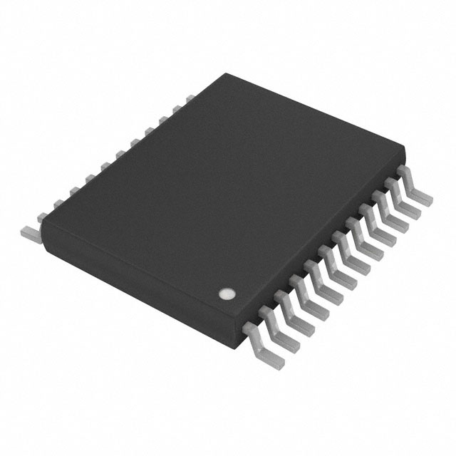


 工商网监
湘ICP备2023018690号
工商网监
湘ICP备2023018690号
