Please note that Cypress is an Infineon Technologies Company.
The document following this cover page is marked as “Cypress” document as this is the
company that originally developed the product. Please note that Infineon will continue
to offer the product to new and existing customers as part of the Infineon product
portfolio.
Continuity of document content
The fact that Infineon offers the following product as part of the Infineon product
portfolio does not lead to any changes to this document. Future revisions will occur
when appropriate, and any changes will be set out on the document history page.
Continuity of ordering part numbers
Infineon continues to support existing part numbers. Please continue to use the
ordering part numbers listed in the datasheet for ordering.
www.infineon.com
�THIS SPEC IS OBSOLETE
Spec No:
002-08413
Spec Title:
MB39A134 DC/DC Converter IC for
Charging Li-ion Battery
Replaced by:
None
�MB39A134
DC/DC Converter IC
for Charging Li-ion Battery
Description
The MB39A134 is a DC/DC converter IC for charging Li-ion battery, which is suitable for down conversion, and uses pulse width
modulation (PWM) for controlling the charge voltage and current independently.
MB39A134 has a AC adapter detection comparator independent of the DC/DC converter controller, and can control the source of
power supply to a system. It supports a wide input voltage range, enables low current consumption in standby mode, and can
control the charge voltage and charge current with high precision, which is perfect for the built-in Li-ion battery charger used in
devices such as notebook PC.
Features
•
•
•
•
•
Support 2, 3 and 4 Cell Battery Pack
Built-in two constant current control loops
Built-in AC adapter detection function (ACOK pin)
Charge voltage accuracy : ±0.7% (Ta = −10° C to +85°C)
Built-in charging voltage control without external setting resistor (4.20 V/Cell or 4.10 V/Cell)
Adjustable to charge voltage with external resistor
• Built-in two high accurate current detection amplifiers (±1%) (At input voltage difference 100 mV)
•
•
•
•
•
•
(±5%) (At input voltage difference 20 mV)
Input offset voltage: 0 mV (Current Amp1)
: +3 mV (Current Amp2)
Built-in Charging Current Control without external resistor (RS = 20 mΩ : 2.85 A)
Adjustable charging current with external resistor
Setting of switching frequency using an external resistor
(Frequency setting capacitor integrated) : 100 kHz to 2 MHz
Built-in under voltage lockout protection
In standby mode (ICC = 6 µA Typ) , only AC adapter detection function is operated
Built-in VH regulator for reducing Qg loss of P-ch MOS FET
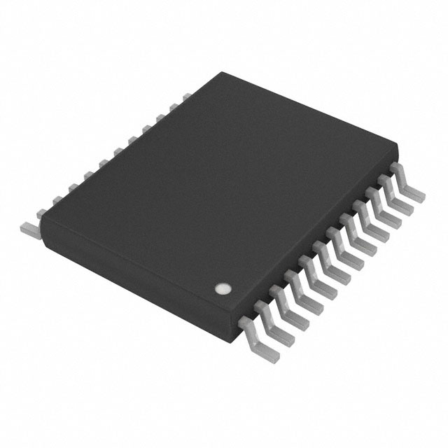
Package : TSSOP-24
Applications
• Built-in charger for Notebook PC
• Handy terminal device etc.
Cypress Semiconductor Corporation
Document Number: 002-08413 Rev. *D
•
198 Champion Court
•
San Jose, CA 95134-1709
•
408-943-2600
Revised December 10, 2018
�MB39A134
Contents
Description ........................................................................ 1
Features ............................................................................. 1
Applications ...................................................................... 1
1. Pin Assignment .............................................................. 3
2. Pin Descriptions ............................................................. 4
3. Block Diagram ............................................................... 5
4. Absolute Maximum Ratings ........................................... 6
5. Recommended Operating Conditions ........................... 7
6. Electrical Characteristics ............................................... 8
7. Typical Characteristics ................................................ 12
8. Functional Description ................................................. 14
8.1 DC/DC Converter Block ..................................... 14
8.2 Protection Functions ........................................... 16
9. Transit Response When A Load Changes Suddenly .. 21
Document Number: 002-08413 Rev. *D
10. Connection Without Using The Current Amp1, Current
Amp2 And The Error Amp1, Error Amp2 ................... 22
11. Input/Output Pin Equivalent Circuit Diagram ............. 23
12. Typical Application Circuit ......................................... 26
13. Application Note ........................................................ 30
14. Reference Data ......................................................... 39
15. Usage Precaution ...................................................... 41
16. Ordering Information .................................................. 41
17. RoHS Compliance Information .................................. 41
18. Package Dimension ................................................... 42
19. Document History ..................................................... 43
Sales, Solutions, and Legal Information ...................... 44
Page 2 of 44
�MB39A134
1. Pin Assignment
(TOP VIEW)
−INC1
1
24
+INC1
OUTC1
2
23
GND
ADJ1
3
22
CVM
COMP1
4
21
VCC
ACOK
5
20
OUT
VREF
6
19
VH
ACIN
7
18
VIN
COMP2
8
17
RT
ADJ2
9
16
ADJ3
OUTC2
10
15
COMP3
CELLS
11
14
CTL
BATT
12
13
+INC2
(STF024)
Document Number: 002-08413 Rev. *D
Page 3 of 44
�MB39A134
2. Pin Descriptions
Pin No. Pin Name
I/O
Description
1
-INC1
I
Current detection amplifier (Current Amp1) inverted input pin.
2
OUTC1
O
Current detection amplifier (Current Amp1) output pin.
3
ADJ1
I
Error amplifier (Error Amp1) non-inverted input pin.
4
COMP1
O
Error amplifier (Error Amp1) output pin.
5
ACOK
O
AC adapter voltage detection block (AC Comp.) output pin.
ACIN = H : ACOK = L, ACIN = L : ACOK = Hi-Z
6
VREF
O
Reference voltage output pin.
7
ACIN
I
AC adapter voltage detection block (AC Comp.) input pin.
8
COMP2
O
Error amplifier (Error Amp2) output pin.
9
ADJ2
I
Charge current control block setting input pin.
ADJ2 pin “GND to 4.4 V” : Charge current control block output = ADJ2 pin
voltage
ADJ2 pin “4.6 V to VREF” : Charge current control block output = 1.5 V
10
OUTC2
O
Current detection amplifier (Current Amp2) output pin.
11
CELLS
I
Charge voltage setting switch pin (2 or 3 or 4 Cells).
CELLS = VREF: 4 Cells, CELLS = GND: 3 Cells, CELLS = OPEN: 2 Cells
12
BATT
I
Current detection amplifier (Current Amp2) inverted input pin.
Battery voltage input pin.
13
+INC2
I
Current detection amplifier (Current Amp2) non-inverted input pin.
14
CTL
I
Power supply control pin.
Setting the CTL pin at “H” level places the DC/DC converter IC in the operating mode.
Setting the CTL pin at “L” level places the DC/DC converter IC in the standby mode.
15
COMP3
O
Error amplifier (Error Amp3) output pin.
16
ADJ3
I
Charge voltage control block setting input pin.
ADJ3 pin “GND to 0.2 V” : Charge voltage setting 4.10 V/Cell
ADJ3 pin “0.4 V to 4.4 V” : Charge voltage setting 2 × VADJ3 pin voltage/Cell
ADJ3 pin “4.6 V to VREF” : Charge voltage setting 4.20 V/Cell
17
RT
Triangular wAVe oscillation frequency setting resistor connection pin.
18
VIN
−
−
19
VH
O
Power supply pin for FET drive circuit (VH = VCC − 6 V)
20
OUT
O
External FET gate drive pin.
21
VCC
−
Power supply pin for reference voltage , control circuit, and output circuit.
22
CVM
O
Constant voltage control state detection block (CV Comp.) output pin.
23
GND
−
Ground pin.
24
+INC1
I
Current detection amplifier (Current Amp1) non-inverted input pin.
Power supply pin for ACOK function block.
Document Number: 002-08413 Rev. *D
Page 4 of 44
�MB39A134
3. Block Diagram
TO SYSTEM
LOAD
CVM
ACIN
ACOK
22 7
VIN
18
−
OUTC1
+
+
2
−
24
1
+
✕ 25
VCC
−
+
+
+
−
−2.5 V
−1.5 V
+
-INC1
3
ADJ1
OUTC2
+INC2
13
12
+
✕ 25
−
9
B
Io
VCC-6 V
2.85 A
VO
19
VH
RS
20 mΩ
Battery
VCC
UVLO
CT
Charge Current
Control
ADJ2
A
OUT
+
3 mV
BATT
20
Drive
Bias
Voltage
10
A
B
21
+INC1
VIN
5
VREF
UVLO
16
ADJ3
VREF :
4.20 V/Cell
GND :
4.10 V/Cell
VO
REFIN
Control
−
+
VCC
VCC
1.26 V
VR1
11
OPEN : 2Cell
GND : 3Cell
VREF : 4Cell
CELLS
Document Number: 002-08413 Rev. *D
4
8
COMP1
15
COMP2
17
COMP3
RT
14
5.0 V ON/OFF
VREF
6
VREF
23
CTL
( 24-pin )
GND
Page 5 of 44
�MB39A134
4. Absolute Maximum Ratings
Parameter
Power supply voltage
Symbol
VvCC
Condition
VCC, VIN pin
VCC, VIN pin, t ≤ 10 µs
Output current
IOUT
OUT pin
OUT pin
Duty ≤ 5% (t = 1/fosc × Duty)
CLT pin input voltage
VCTL
CTL pin
Input voltage
VINE
ADJ1, ADJ2, ADJ3, CELLS, ACIN
pin
VINC
-INC1, +INC1, BATT, +INC2 pin
Power dissipation
Storage temperature
PD
Ta ≤
+ 25°
Ta = + 85°
TSTG
−
Rating
Unit
Min
Max
− 0.3
− 0.3
− 60
− 700
+ 28
+ 32
+ 60
+ 700
− 0.3
− 0.3
+ 28
VVREF + 0.3
V
− 0.3
−
−
− 55
+ 28
V
1282*1,*2
mW
512*1,*2
mW
+ 125
°C
V
V
mA
mA
V
*1 : See the diagram of “Typical Characteristics. Maximum Power Dissipation vs. Operating Ambient Temperature”, for the package
power dissipation of Ta from + 25° C to + 85° C.
*2 : When IC is mounted on a 10x10 cm two-layer square epoxy board.
WARNING: Semiconductor devices can be permanently damaged by application of stress (voltage, current,
temperature, etc.) in excess of absolute maximum ratings. Do not exceed these ratings.
Document Number: 002-08413 Rev. *D
Page 6 of 44
�MB39A134
5. Recommended Operating Conditions
Parameter
Symbol
Power supply voltage
VVCC
Reference voltage output current
IVREF
VH pin output current
Input voltage
Condition
Typ
Max
8
25
V
0
mA
30
mA
0
−
−
−
−
VVREF −
1.5
V
4.6
−
VVREF
V
ADJ2 pin
(external voltage setting)
0
−
4.4
V
ADJ3 pin
(internal reference voltage
setting)
0
−
0.2
V
VVREF
V
VCC, VIN pin
−
−
ADJ1 pin
ADJ2 pin
(internal reference voltage
setting)
ACIN pin input voltage
VACIN
ACOK pin output voltage
VACOK
ACOK pin output current
IACOK
CTL pin input voltage
VCTL
Output current
IOUT
fOSC
Timing resistor
RRT
VH pin capacitor
CVH
Reference voltage output
capacitor
Operating ambient
temperature
CVREF
Ta
0
4.6
−
4.4
V
CELLS pin
0
VVREF
V
+INC1, +INC2, -INC1, BATT
0
−
−
VVCC
V
5
V
25
V
1
mA
25
V
−45
−600
−
−
−
−
−
−
+ 45
+ 600
mA
mA
100
500
2000
kHz
8.2
33
180
kΩ
−
−
0.1
1.0
µF
0.1
1.0
µF
−30
+ 25
+ 85
°C
pin
−
−
−
−
OUT pin
OUT pin
Duty ≤ 5% (t = 1 / fosc × Duty)
Switching frequency
−1
0.4
ADJ3 pin
(external voltage setting)
VINC
Unit
Min
IVH
VINE
Value
−
RT pin
−
VREF pin
−
0
0
0
0
WARNING: The recommended operating conditions are required in order to ensure the normal operation of the semiconductor
device. All of the device's electrical characteristics are warranted when the device is operated within these ranges.
Always use semiconductor devices within their recommended operating condition ranges. Operation outside these
ranges may adversely affect reliability and could result in device failure.
No warranty is made with respect to uses, operating conditions, or combinations not represented on the data sheet.
Users considering application outside the listed conditions are advised to contact their representatives beforehand.
Document Number: 002-08413 Rev. *D
Page 7 of 44
�MB39A134
6. Electrical Characteristics
Parameter
Reference
Voltage Block
[REF]
Triangular Wave
Oscillator Block
[OSC]
Error Amplifier
Block
[Error Amp1]
Symbol
Pin
No.
VVREF1
VVREF2
6
Input stability
VREF
Line
6
Load stability
VREF
Load
Short-circuit
output
current
Threshold
voltage
(Ta = +25°, VCC pin = 19 V, VREF pin = 0 mA)
Value
Condition
Unit
Min
Typ
Max
−
4.963
5.000
5.037
V
4.950
5.000
5.050
V
VCC pin = 8 V to 25 V
−
3
10
mV
6
VREF pin = 0 mA to −1 mA
−
1
10
mV
Ios
6
VREF pin = 1 V
−25
−12
−6
mA
fOSC
20
RT pin = 33 kΩ
450
500
550
kHz
Frequency
temperature
variation
df/fdT
20
Ta = −30° to +85°
−
1*
−
%
Input offset
voltage
VIO
2, 3
COMP1 pin = 2 V
−
1
5
mV
Input bias
voltage
IADJ1
3
ADJ1 pin = 0 V
−100
−
−
nA
Gm
15
−
−
20*
−
µA/V
VTH1
10
−
1.5*
−
V
Gm
15
−
20*
−
µA/V
VTH1
12
COMP3 pin = 2 V,
Ta = +25°
ADJ3 pin = VREF pin
(4.20 V/Cell setting)
−0.5
0
+ 0.5
%
VTH2
12
COMP3 pin = 2 V,
Ta = −10° to +85°,
ADJ3 pin = VREF pin
(4.20 V/Cell setting)
−0.7
0
+ 0.7
%
VTH3
12
COMP3 pin = 2 V,
Ta = +25°
ADJ3 pin = GND,
(4.10 V/Cell setting)
−0.6
0
+ 0.6
%
VTH4
12
COMP3 pin = 2 V,
Ta = − 10° to +85°
ADJ3 pin = GND,
(4.10 V/Cell setting)
−0.8
0
+ 0.8
%
Switching
frequency
Transconductance
Error Amplifier
Block
[Error Amp2]
Threshold
voltage
Error Amplifier
Block
[Error Amp3]
Threshold
voltage
accuracy
Transconductance
Document Number: 002-08413 Rev. *D
6
Ta = −10° to +85°
ADJ2 pin = VREF pin
−
Page 8 of 44
�MB39A134
Symbol
Pin
No.
IBATTH1
12
ADJ3 pin = CELLS pin =
VREF pin
BATT pin = 16.8 V
−
25.2
38
μA
IBATTL
12
VCC pin = 0 V, BATT pin =
16.8 V
−
0
1
μA
Transconductance
Gm
15
−
−
30*
−
μA/V
Input current
I+INCH
13, 24
−
20
30
μA
I−INCH
1
−
0.1
0.2
μA
I+INCL
13, 24
−225 −150
−
μA
I−INCL
1
−255 −170
−
μA
VOFF1
2
VOFF2
10
VOFF3
10
VCM
2, 10
+INC1 pin = +INC2 pin = 3 V to
VCC pin, ΔVin = −100 mV
+INC1 pin = 3 V to VCC pin,
ΔVin = −100 mV
+INC1 pin = +INC2 pin = 0.1 V,
ΔVin = −100 mV
+INC1 pin = +INC2 pin = 0.1 V,
ΔVin = −100 mV
+INC1 pin = 3 V to VCC pin
+INC2 pin = 3 V to VCC pin
+INC2 pin = 0 V to 3 V
−
Voltage gain
AV
2, 10
Frequency band
width
BW
2, 10
Parameter
Error Amplifier
Block
[Error Amp3]
Current
Detection
Amplifier Block
[Current Amp1,
Current Amp2]
Input current
Input offset
voltage
−1
0
1
mV
2
3
4
mV
1
3
5
mV
0
−
Vvcc
V
24.5
25.0
25.5
V/V
−
2*
−
MHz
VOUTCH1
2
−
VOUTCH2 10
−
VOUTCL 2, 10
−
ISOURCE 2, 10 OUTC1 pin = OUTC2 pin = 2 V
4.7
4.9
V
4.5
4.7
−
−
50
75
100
mV
−
−2
−1
mA
OUTC1 pin = OUTC2 pin = 2 V
150
300
−
µA
1.4
1.5
−
V
−
2.5
2.6
V
Common mode
input
voltage range
Output voltage
Output source
current
PWM Comp.
Block
[PWM Comp.]
(Ta = +25°, VCC pin = 19 V, VREF pin = 0 mA)
Value
Condition
Unit
Min Typ Max
+INC1 pin = +INC2 pin = 3 V to
VCC pin, ΔVin = −100 mV
AV = 0 dB
Output sink
current
ISINK
2, 10
Threshold
voltage
VTL
VTH
20
Duty cycle = 0%
20
Duty cycle = 100%
Document Number: 002-08413 Rev. *D
V
Page 9 of 44
�MB39A134
Symbol
Pin
No.
ISOURCE
20
Output sink
current
ISINK
20
Output ON
resistance
ROH
ROL
20
tr1
20
Parameter
Output Block
[OUT]
Output source
current
mA
−
400*
−
mA
6.5
9.8
Ω
5.0
7.5
Ω
50*
−
−
ns
tf1
20
OUT pin = 3300 pF
14
IC operation mode
2
14
IC standby mode
0
14
CTL pin = 5 V
19
VCC pin = 8 V to 25 V,
VH pin = 0 to 30 mA
−
−
VTLH
21
VCC pin =
VTHL
21
Output
voltage
Under Voltage
Lockout
Protection
Circuit Block
[UVLO]
Threshold
voltage
AC Adapter
Voltage
Detection Block
[AC Comp.]
−
VON
VOFF
ICTLH
ICTLL
VH
Hysteresis width
20
14
OUT pin = −45 mA
−400*
CTL input
voltage
Bias Voltage
Block
[VH]
Detection
OUT pin = 19V,
Duty ≤ 5%
(t = 1/fosc ∞ Duty)
−
Fall time
Input current
Over
Temperature
OUT pin = 13 V,
Duty ≤ 5%
(t = 1/fosc ∞ Duty)
−
−
−
−
Rise time
Control Block
[CTL]
(Ta = +25°, VCC pin = 19 V, VREF pin = 0 mA)
Value
Condition
Unit
Min.
Typ. Max.
OUT pin = 45 mA
OUT pin = 3300 pF
CTL pin = 0 V
VCC pin =
µA
0
1
µA
VVCC− VVCC− VVCC−
6.5
6.0
5.5
V
6.0
6.2
6.4
V
5.0
5.2
5.4
V
V
2.4
2.6
2.8
V
0.2
+ 150
−
−
V
−
−
−
°C
−
−
+ 125
−
°C
1.245
1.270
1.295
V
1.215
1.250
1.285
V
−
−
20
−
mV
5
−
−
−
ACOK pin = 25 V
0
1
µA
VACOKL
5
ACOK pin = 1 mA
−
0.9
1.1
V
IVINL
18
VIN pin = 19 V,
ACIN pin = 0 V
−
0
1
µA
IVINH
18
−
6
10
µA
Hysteresis width
VH
6
VREF pin
Detection
temperature
TTH
20
Release
temperature
TTL
20
VTLH
VTHL
VH
ILEAK
7
Document Number: 002-08413 Rev. *D
150
V
VREF pin =
consumption
100
−
6
Current
V
3.0
VTHL
ACOK pin
output “L”
level voltage
0.8
2.8
VREF pin =
Hysteresis width
V
1.0*
VCC pin
6
ACOK
pin
output leak
current
25
−
21
Threshold
voltage
ns
2.6
VH
VTLH
Threshold
voltage
50*
7
7
VIN pin = 19 V,
ACIN pin = 5 V
Page 10 of 44
�MB39A134
Parameter
Charge Voltage
Control Block
[VO REFIN
Control]
Symbol Pin No.
Input voltage
Threshold
voltage
Input current
Input voltage
Input current
Charge Current
Control Block
[Charge Current
Control]
Input voltage
General
Standby
current
Threshold
voltage
Input current
(Ta = +25°, VCC pin = 19 V, VREF pin = 0 mA)
Value
Condition
Unit
Min.
Typ.
Max.
VVREF
V
4.4
V
0
−
−
−
0.2
V
0.21
0.3
0.39
V
4.41
4.5
4.59
V
−
0
1
µA
VH
VEXT
VL
VTL
VTH
IIN
VH
16
At 4.20 V/Cell
4.6
16
At external setting
0.4
16
At 4.10 V/Cell
−
−
16
16
16
ADJ3 pin
11
At 4 Cells
VVREF −
0.4
−
VVREF
V
VM
VL
IINL
IINH
11
At 2 Cells
2.4
2.6
V
11
At 3 Cells
0
0.3
V
11
CELLS = 0 V
−
µA
11
CELLS = IVREF
−
−
−5
5
8.3
µA
VH
9
At normal charge
4.6
VVREF
V
VEXT
9
At external setting
0
−
−
4.4
V
VTH
9
4.41
4.50
4.59
V
−
−
0
1
µA
6
10
µA
−
0
1
µA
4.0
mA
−
IIN
9
ADJ2 pin
ICCS1
18
VCC pin = 0 V,
CTL pin = 0 V,
ACIN pin = 5 V,
VIN pin = 19 V
ICCS2
21
VIN pin = 0 V,
CTL pin = 0 V,
VCC pin = 19 V
−8.3
−
Power supply
ICC
21
CTL pin = 5 V
−
2.7
current
*: This parameter isn't be specified. This should be used as a reference to support designing the circuits.
Document Number: 002-08413 Rev. *D
Page 11 of 44
�MB39A134
7. Typical Characteristics
4
3
2
Ta = +25 °C
VCTL = 5 V
1
0
5
10
15
20
25
3
2
Ta = +25 °C
VCTL = 5 V
IVREF = 0 mA
1
0
5
10
15
20
25
600
6
VVREF
500
5
400
4
300
3
ICTL
200
2
100
1
0
0
5
10
15
20
0
25
6
Ta = +25 °C
VVCC = 19 V
VCTL = 5 V
5
4
3
2
1
0
0
5
10
15
20
25
Power supply voltage VVCC (V)
Load current IVREF (mA)
Reference voltage vs.
Operating ambient temperature
Triangular wave oscillation frequency vs. Power supply voltage
5.08
VVCC = 19 V
VCTL = 5 V
IVREF = 0 mA
5.06
5.04
5.02
5.00
4.98
4.96
4.94
4.92
−40
8
7
Reference voltage vs.
Load current
4
9
700
Reference voltage vs.
Power supply voltage
5
0
800
CTL pin input voltage VCTL (V)
6
10
Ta = +25 °C
VVCC = 19 V
IVREF = 0 mA
900
Power supply voltage VVCC (V)
Reference voltage VVREF (V)
0
1000
−20
0
+20
+40
+60
+80
+100
Operating ambient temperature Ta (°C)
Document Number: 002-08413 Rev. *D
Reference voltage VVREF (V)
5
CTL pin input current ICTL (μA)
CTL pin input current, Reference voltage
vs. CTL pin input voltage
Triangular wave oscillation
frequency fosc (kHz)
Reference voltage VVREF (V)
Reference voltage VVREF (V)
Power supply current ICC (mA)
Power supply current vs.
Power supply voltage
550
540
Ta = +25 °C
VCTL = 5 V
RT = 33 kΩ
530
520
510
500
490
480
470
460
450
0
5
10
15
20
25
Power supply voltage VVCC (V)
Page 12 of 44
�MB39A134
Triangular wave oscillation frequency vs. Operating ambient temperature
Triangular wave oscillation frequency vs. Timing resistor
VVCC = 19 V
VCTL = 5 V
RT = 33 kΩ
−20
0
+20
+40
+60
+80
+100
Triangular wave oscillation
frequency fosc (kHz)
Triangular wave oscillation
frequency fosc (kHz)
10000
550
540
530
520
510
500
490
480
470
460
450
−40
Ta = +25 °C
VVCC = 19 V
VCTL = 5 V
1000
100
10
10
100
1000
Error amplifier threshold voltage vs.
Operating ambient temperature
Error amplifier threshold voltage vs.
Operating ambient temperature
8.500
VVCC = 19 V
VCTL = 5 V
VCELLS = OPEN
8.475
8.450
8.425
8.400
8.375
8.350
8.325
8.300
−40
−20
0
+20
+40
+60
+80 +100
Error amplifier threshold voltage
VTH (V)
Timing resistor RT (kΩ)
12.700
VVCC = 19 V
VCTL = 5 V
VCELLS = GND
12.675
12.650
12.625
12.600
12.575
12.550
12.525
12.500
−40
−20
0
+20
+40
+60
+80 +100
Operating ambient temperature Ta (°C)
Operating ambient temperature Ta (°C)
Error amplifier threshold voltage vs.
Operating ambient temperature
Permissible dissipation vs.
Operating ambient temperature
16.900
VVCC = 19 V
VCTL = 5 V
VCELLS = 5 V
16.875
16.850
16.825
16.800
16.775
16.750
16.725
16.700
-40
-20
0
+20
+40
+60
+80 +100
Operating ambient temperature Ta (°C)
Document Number: 002-08413 Rev. *D
Permissible dissipation PD (mW)
Error amplifier threshold voltage
VTH (V)
Error amplifier threshold voltage
VTH (V)
1
Operating ambient temperature Ta (°C)
1400
1282
1200
1000
800
600
400
200
0
−40
−20
0
+20
+40
+60
+80
+100
Operating ambient temperature Ta (°C)
Page 13 of 44
�MB39A134
8. Functional Description
MB39A134 is a DC/DC converter which uses pulse width modulation (PWM) for charging Li-ion battery and controls the charge
voltage and current when charging the battery. It includes the charge control function for the battery and the AC adapter voltage
detection function to stably supply the voltage from the AC adapter and the battery to the system.
When controlling the charge voltage (constant voltage mode), the voltage entered in ADJ3 pin and CELLS pin can be used to set
an arbitrary voltage. The error amplifier (Error Amp3) compares BATT pin voltage with the internal reference voltage to generate
the PWM control signal for generating an arbitrary charge voltage.
When controlling the charge current (constant current mode), the current detection amplifier (Current Amp2) amplifies the voltage
drop generated between both ends of the charge current sense resistance (RS) to 25 times and outputs it through OUTC2 pin.
The error amplifier (Error Amp2) compares the output voltage from the current detection amplifier (Current Amp2) with the voltage
set at ADJ2 pin to generate the PWM control signal for executing the constant current charge.
When controlling the AC adapter power, the current detection amplifier (Current Amp1) amplifies the difference between -INC1
pin voltage and +INC1 pin voltage (VVREF) to 25 times and outputs it through OUTC1 pin when the output voltage of the AC
adapter drops. The error amplifier (Error Amp1) compares the output voltage from the current detection amplifier (Current Amp1)
with ADJ1 pin voltage to generate the PWM control signal for controlling the charge current so that AC adapter power can be kept
constant.
The triangular wave voltage generated from the triangular wave oscillator is compared with the lowest potential of the output
voltages from the error amplifier (Error Amp1, Error Amp2, and Error Amp3) and when the former is lower than the latter, the high
side switching FET is set on.
In addition, AC Comp detects installation/removal of the AC adapter and its information is generated through ACOK pin.
8.1
8.1.1
DC/DC Converter Block
Reference Voltage Block (REF)
The reference voltage circuit (REF) uses the voltage supplied from the VCC pin (pin 21) to generate stable voltage (Typ 5.0 V) that
has undergone temperature compensation. The generated voltage is used as the reference power supply for the internal circuitry of
the IC.
This block can output load current of up to 1 mA from the reference voltage VREF pin (pin 6).
8.1.2
Triangular Wave Oscillator Block (OSC)
The triangular wave oscillator builds the capacitor for frequency setting into, and generates the triangular wave oscillation waveform
by connecting the frequency setting resistor with the RT pin (pin 17). The triangular wave is input to the PWM comparator on the IC.
Triangular wave oscillation frequency: fosc
fosc (kHz) ≈ 17000 / RT (kΩ)
8.1.3
Error Amplifier Block (Error Amp1)
This amplifier detects the output signal from the current detection amplifier (Current Amp1) and outputs a PWM control signal.
In addition, a stable phase compensation can be made available to the system by connecting the resistor and the capacitor to the
COMP1 pin.
8.1.4
Error Amplifier Block (Error Amp2)
This amplifier detects the output signal from the current detection amplifier (Current Amp2), compares this to the output signal from
the charge current control circuit, and outputs a PWM control signal to be used in controlling the charge current.
In addition, a stable phase compensation can be made available to the system by connecting the resistor and the capacitor to the
COMP2 pin.
Document Number: 002-08413 Rev. *D
Page 14 of 44
�MB39A134
8.1.5
Error Amplifier Block (Error Amp3)
This error amplifier (Error Amp3) detects the output voltage from the DC/DC converter, compares this to the output signal from the
VO REFIN controller circuit, and outputs the PWM control signal.
Arbitrary output voltage from 2 Cell to 4 Cell can be set by connecting an external resistor of charging voltage to ADJ3 pin (pin 16).
In addition, a stable phase compensation can be made available to the system by connecting the resistor and the capacitor to the
COMP3 pin.
8.1.6
Current Detection Amplifier Block (Current Amp1)
The current detection amplifier (Current Amp1) amplifies the voltage difference between +INC1 pin (pin 24) and -INC1 pin (pin 1) 25
times and the signal is output to the following error amplifier (Error Amp1) .
8.1.7
Current Detection Amplifier Block (Current Amp2)
The current detection amplifier (Current Amp2) detects a voltage drop on the both ends of the output sense resistor (RS) due to the
flow of the charge current, using the +INC2 pin (pin 13) and BATT pin (pin 12). The signal amplified to 25 times is output to the
following error amplifier (Error Amp2).
8.1.8
PWM Comparator Block (PWM Comp.)
The PWM comparator circuit (PWM Comp.) is a voltage-pulse width converter for controlling the output duty of the error amplifiers
(Error Amp1 to Error Amp3) depending on their output voltage.
The PWM comparator circuit compares the triangular wave voltage generated by the triangular wave oscillator with the error
amplifier output voltage and turns on the external output transistor (MOS FET) , during the interval in which the triangular wave
voltage is lower than the error amplifier output voltage.
8.1.9
Output Block (OUT)
The output circuit uses a totem-pole configuration capable of driving an external P-ch MOS FET.
The output “L” level sets the output amplitude to 6 V (Typ) using the voltage generated by the bias voltage block (VH) .
This results in increasing conversion efficiency and suppressing the withstand voltage of the connected external transistor
(MOSFET) even in a wide range of input voltages.
8.1.10
Power Supply Control Block (CTL)
Setting the CTL pin (pin 14) to “L” level places the IC in the standby mode. During the standby mode, only AC adapter detection
function is operated. (The supply current is 6 µA at typical in the standby mode.)
Table 1. CTL Function Table
CTL
Power
AC Adapter Detection
L
OFF (Standby)
ON (Active)
H
ON (Active)
ON (Active)
8.1.11
Bias Voltage Block (VH)
The bias voltage circuit outputs VVCC − 6 V (Typ) as the minimum potential of the output circuit. In the standby mode, this circuit
outputs the potential equal to VVCC.
Document Number: 002-08413 Rev. *D
Page 15 of 44
�MB39A134
8.2
Protection Functions
8.2.1
Under Voltage Lockout Protection Circuit Block (UVLO)
The transient state or a momentary decrease in supply voltage or internal reference voltage (VREF pin),
which occurs when the power supply (VCC pin) is turned on, may cause malfunctions in the control IC, resulting in breakdown or
deterioration of the system.
To prevent such malfunction, the under voltage lockout protection circuit detects internal reference voltage drop and fixes the OUT
pin (pin 20) to the “H” level. The system restores when the power supply and the internal reference reaches less than the threshold
voltage of the lockout protection circuit at the low voltage level.
Protection circuit (UVLO) operation function table
When UVLO is operating (VCC or VREF voltage is lower than UVLO threshold voltage.), the logic of the following pin is fixed at the
value shown.
pin
OUT
Status
H
8.2.2
Over Temperature Detection
The circuit protects an IC from heat-destruction. If the temperature at the joint part reaches +150°C, the circuit changes the level of
OUT pin to “H”, and stops the voltage output.
In addition, if the temperature at the joint part drops to +125°C, the output restarts again.
Therefore, make sure to design the DC/DC power supply system so that the over heating protection does not start frequently.
8.2.3
Detection Functions
AC adapter voltage detection block (AC Comp.)
The AC adapter voltage detection block (AC Comp.) detects that ACIN pin voltage is below 1.25 V (Typ)
and sets ACOK pin in the AC adapter voltage detection block to Hi-Z. In addition, a higher voltage from either VCC pin or VIN pin is
supplied as the IC power supply.
ACIN
ACOK
H
L
L
Hi-Z
R1
Micro
controller
AC adapter
R2
7
ACIN
5
ACOK
+
−
Document Number: 002-08413 Rev. *D
Page 16 of 44
�MB39A134
AC adapter detection voltage setting
VIN = Low to High
Vth = (R1 + R2) / R2 × 1.27 V
VIN = High to Low
Vth = (R1 + R2) / R2 × 1.25 V
8.2.4
Setting the Charge Voltage
The charge voltage (DC/DC output) is set by the input voltage to ADJ3 pin (pin 16) and CELLS pin (pin 11). The ADJ3 pin (pin 16)
can set charge voltage per cell. An arbitrary charge voltage is set when external resistor is set. It does not need external resistor
when ADJ3 pin (pin 16) is input to VREF level or GND level by internal high accurate reference voltage. The CELLS pin (pin 11) can
set the series battery number when the pin is input VREF, OPEN or GND level.
The setting of ADJ3 pin (pin 16), CELLS pin (pin 11) and charge voltage (DC/DC output) is shown below.
ADJ3 Input Voltage
CELLS
VREF pin
(ADJ3 ≥4.6 V)
GND pin
(ADJ3 ≤ 0.2 V)
External voltage setting
(ADJ3 = 0.4 V to 4.4 V)
Charge Voltage
Note
OPEN
8.4 V
2 Cell × 4.20 V/Cell
GND
12.6 V
3 Cell × 4.20 V/Cell
VREF
16.8 V
4 Cell × 4.20 V/Cell
OPEN
8.2 V
2 Cell × 4.10 V/Cell
GND
12.3 V
3 Cell × 4.10 V/Cell
VREF
16.4 V
4 Cell × 4.10 V/Cell
OPEN
4 × ADJ3 pin voltage
2 Cell × 2 × ADJ3 pin voltage/Cell
GND
6 × ADJ3 pin voltage
3 Cell × 2 × ADJ3 pin voltage/Cell
VREF
8 × ADJ3 pin voltage
4 Cell × 2 × ADJ3 pin voltage/Cell
• ADJ3 Pin Internal Circuit
ADJ3
VA
VA
16
+
2.1 V
Comparator_A
To Error Amp3
SELECTOR
2.05 V
−
4.5 V
LOGIC
+
Comparator_B
−
0.3 V
Document Number: 002-08413 Rev. *D
Page 17 of 44
�MB39A134
8.2.5
Setting the Charge Current
The Error amplifier block (Error Amp2) compares the output voltage of charge current control block set by ADJ2 pin (pin 9) with the
output signal from the current detection amplifier (current Amp2) , and outputs a PWM control signal to be used in controlling the
maximum charge current for battery. When the current overflows the rated value, the current will be constantly charged to the rated
value, and the charge voltage will drop.
Battery charge current setting voltage : ADJ2
Charge current control block output voltage (V)
Upper limit of charge current Io =
− 0.075
Current detection amplifier block voltage gain (25.0 V/V Typ) ×
sense resistor RS (Ω)
Charge Current
Control Block
Output Voltage
RS = 40 mΩ
RS = 20 mΩ
RS = 15 mΩ
VREF
(ADJ2 > 4.6 V)
1.5 V
1.425 A
2.85 A
3.79 A
External Voltage Setting
(ADJ2 = GND to 4.4 V)
VADJ2
(V)
VADJ2-0.075
(A)
2 × (VADJ2-0.075)
(A)
2.66 × (VADJ2-0.075)
(A)
ADJ2 Input Voltage
Charge Current
• ADJ2 Pin Internal Circuit
ADJ2
To Error Amp2
9
1.5 V
Selector
Comparator_C
+
−
4.5 V
Document Number: 002-08413 Rev. *D
Page 18 of 44
�MB39A134
• Example of charge current setting (RS = 40 mΩ)
Io
4.4 V
4.325 A
1.425 A
0V
4.41 V
4.59 V
External setting when ADJ2 = 0 V to 4.4 V
VADJ2
VVREF
Internal reference voltage setting when ADJ2 = 4.6 V to VREF
Io (mA)
600
500
400
At RS = 40 mΩ,
+INC1 = 3 V to VCC
300
200
100
Error (MB39A134) < ±25 mA
VADJ2 (mV)
100 200 300 400 500 600
Max VADJ2 < 100 mV at Io = 0 mA
Typ VADJ2 = 75 mV at Io = 0 mA
Min VADJ2 > 50 mV at Io = 0 mA
Io = 0 mA at VADJ2 = 0 V
Document Number: 002-08413 Rev. *D
Page 19 of 44
�MB39A134
8.2.6
Setting Dynamically-Controlled-Charging
By connecting as shown in the example of the figure below, the AC adopter voltage (VIN) drops and becomes the calculated Vth,
and then, the dynamically-controlled charging loop reduce the charge current to keep a settled power level.
AC adopter voltage in dynamically controlled charging mode:
Vth = VREF × (1 −
1
AV
R4
×
R3 + R4
VREF : Reference voltage (5.0 V Typ)
VIN
R1 + R2
)×
R2
AV : Current detection amplifier block voltage gain (25.0 V/V Typ)
VREF (5 V)
+INC1
R1
24
+
1
−
−INC1
R2
−
+
R3
ADJ1
3
R4
Document Number: 002-08413 Rev. *D
Page 20 of 44
�MB39A134
9. Transit Response When a Load Changes Suddenly
The constant voltage control loop and the constant current control loop are independent each other and when a load changes
suddenly, these two control loops switch over each other.
Overshoot of the battery voltage and current is generated by the delay in the control loop when changing the mode.
The delay time is determined by the phase compensation components values.
When the constant current control switches over to the constant voltage control when removing the battery, the control period with
higher duty than the rated charge voltage occurs, resulting in voltage overshoot. In such a period, since the battery is removed, no
excessive voltage should be applied to the battery.
When the constant voltage control switches over to the constant current control when installing the battery, the control period with
higher duty than the rated charge current occurs, resulting in current overshoot.
For MB39A134, it can not be as current overshoot with 10 ms or less.
Error Amp3 Output
Error Amp2 Output
Constant Current
Battery Voltage
Battery Current
Error Amp2 Output
Error Amp3 Output
Low Voltage
Constant Current
When the charge control switches
over from the constant current control
to the constant voltage control, the
control period with higher duty than
the rated charge voltage occurs,
resulting in voltage overshoot.
For MB39A134, it can not be
as current overshoot with 10
ms or less.
10 ms
Document Number: 002-08413 Rev. *D
Page 21 of 44
�MB39A134
10. Connection Without Using The Current Amp1, Current Amp2 and
The Error Amp1, Error Amp2
When Current Amp1, 2 or Error Amp1, 2 are not used, please connect it as follows.
• +INC1 pin (pin 24), -INC1 pin (pin 1), ADJ1 pin (pin 3), and ADJ2 pin (pin 9) are connected with the VREF pin.
• +INC2 pin (pin 13) is connected with the pin BATT pin (pin 12).
• OUTC1 pin (pin 2) and OUTC2 pin (pin10) open.
24
+INC1
+INC2
13
1
-INC1
BATT
12
“OPEN”
2
OUTC1
“OPEN”
10
OUTC2
6
VREF
3
ADJ1
9
ADJ2
4
COMP1
8
COMP2
“OPEN”
“OPEN”
Document Number: 002-08413 Rev. *D
Page 22 of 44
�MB39A134
11. Input/Output Pin Equivalent Circuit Diagram
VCC 21
CTL 14
ESD protection
component
6
VREF
33.1 kΩ
37.27 kΩ
51 kΩ
12.10 kΩ
GND 23
GND 23
VREF 6
VREF 6
4 COMP1
OUTC1 2
17 RT
GND 23
GND 23
3 ADJ1
VREF 6
VREF 6
8 COMP2
OUTC2 10
15 COMP3
-INE3
GND 23
GND 23
+INE2
+INE3
VCC 21
VCC 21
VREF 6
VREF 6
+INC2 13
+INC1 24
10 OUTC2
2 OUTC1
40 kΩ
40 kΩ
7.7 kΩ
10 kΩ
GND 23
10 kΩ
GND 23
1 -INC1
Document Number: 002-08413 Rev. *D
12 BATT
Page 23 of 44
�MB39A134
VREF
6
VCC 21
COMP1 4
20 OUT
CT
COMP2 8
COMP3 15
VH 19
GND 23
GND 23
VCC 21
VIN 18
ACIN
5 ACOK
7
GND 23
VREF
VCC 21
6
SELECTER
100 kΩ
ADJ3 16
19 VH
+INE3
4.5V
0.3V
GND 23
Document Number: 002-08413 Rev. *D
GND 23
Page 24 of 44
�MB39A134
VREF
6
SELECTER
+INE2
9
ADJ2
4.5 V
GND
23
BATT 12
VREF
6
1 MΩ
CELLS 11
-INE3
1 MΩ
GND
GND 23
Document Number: 002-08413 Rev. *D
Page 25 of 44
�MB39A134
12. Typical Application Circuit
Q3
TPCA8102
VSYS
R26 47 kΩ
TPCA8102
Q2A
VIN
R20
6.2 kΩ
R21
91 kΩ
R22
10 kΩ
GND
TPCA8102
Q2B
Q1-2 *2
Wire short
R1
L1
Q1-1
μPA2714GR
C1
10 μF
C15
R23
0.22
200 kΩ μF
R25 *1
C17 *2
15 μH
CDRH104R-150
Vo
20 mΩ
D1
MBRA340T3
R24
100 kΩ
R27
10 kΩ
DTr2 *2
R2
C2
C3
22 μF
*2
DTr1
DTC144EET1G
R48 *2
GND
ACOK
ACOFF
R34 *2
R47
100 kΩ
R30 *1
R28 *1
SW1-1
CTL
C19 *2
R4
1 kΩ
C4
0.022 μF
R43
11 kΩ
R44
240 kΩ
R45
100 kΩ
C5 *2
+INC2
14
CTL
CELLS 11
15
COMP3
OUTC2 10
16
ADJ3
R5
56 kΩ
17
RT
C21
0.1 μF
18
VIN
19
VH
R6
C6
0.1 μF *1
20
21
C7
0.1 μF
CVM
R8
cut
R11 R7
cut 100 kΩ
R46
0Ω
BATT 12
ADJ2
9
COMP2
8
ACIN
7
VREF
6
OUT
ACOK
5
VCC
COMP1
4
22
CVM
ADJ1
3
23
GND
OUTC1
2
24
+INC1
−INC1
1
R35 *1
R32 *1
SGND
13
MB39A134
C8
*2
+INC1
5V
−INC1
18 V
C20 *2
CELLS
OUTC2
R9
10 kΩ
ADJ2
C9
0.001 μF
C10 *2
VREF
R10
10 kΩ
C11
0.1 μF
C12
0.001 μF
C13 *2
OUTC1
C14
*2
R12
*1
R14
100 kΩ
R13
*2
R15
10 kΩ
R16
100 kΩ
SW1-2
R17
*2
R18
0Ω
R19
*2
SW1-2
IO
off
2.85 A
*1 Patterm short
*2 Not mounted
Place R12 = 0 Ω for output 4.2 V/Cell.
Place R13 = 0 Ω for output 4.1 V/Cell.
Document Number: 002-08413 Rev. *D
Page 26 of 44
�MB39A134
• Parts List
ComItem
ponent
M1
IC
Specification
Vendor
Package
Parts No.
MB39A134
Cypress
TSSOP-24
−
Q1-1
P-ch FET
VDS = − 20 V,
ID = 7 A (Max)
RENESAS
SOP-8
Q1-2
P-ch FET
−
−
Q2A
P-ch FET
TOSHIBA
SOP
Advance
TPCA8102
Q2B
P-ch FET
TOSHIBA
SOP
Advance
TPCA8102
Q3
P-ch FET
TOSHIBA
SOP
Advance
TPCA8102
DTr1
Transistor
ON Semi
SC-75
DTr2
Transistor
−
VDS = − 30 V,
ID = 40 A (Max)
VDS = − 30 V,
ID = 40 A (Max)
VDS = − 30 V,
ID = 40 A (Max)
VCEO = 50 V
−
VF = 0.45 V (Max)
at IF = 3 A
−
−
ON Semi
RMDS
μPA2714GR
−
−
Diode
L1
Inductor
15 µH 50 mW
Irms = 3.1 A
SUMIDA
SMD
CDRH104R-150
C1
Ceramic Capacitor
10 µF (25 V)
TDK
3225
C3225X5R1E106K
C2
Ceramic Capacitor
22 µF (25 V)
TDK
3225
C3225JC1E226M
C3
Ceramic Capacitor
−
−
−
C4
Ceramic Capacitor
0.022 µF (50 V)
TDK
1608
C5
Ceramic Capacitor
−
−
−
C6
Ceramic Capacitor
0.1 µF (50 V)
TDK
1608
C1608JB1H104K
C7
Ceramic Capacitor
0.1 µF (50 V)
TDK
1608
C1608JB1H104K
C8
Ceramic Capacitor
−
−
−
C9
Ceramic Capacitor
0.001 µF (50 V)
TDK
1608
C10
Ceramic Capacitor
−
−
−
C11
Ceramic Capacitor
0.1 µF (50 V)
TDK
1608
C1608JB1H104K
C12
Ceramic Capacitor
0.001 µF (50 V)
TDK
1608
C1608JB1H102J
C13
Ceramic Capacitor
C14
Ceramic Capacitor
−
−
−
−
−
−
C15
Ceramic Capacitor
0.22 µF (25 V)
TDK
1608
−
−
−
−
−
−
TDK
1608
−
C19
Ceramic Capacitor
C20
Ceramic Capacitor
−
−
−
C21
Ceramic Capacitor
0.1 µF (50 V)
Document Number: 002-08413 Rev. *D
Not mounted
DTC144EET1G
D1
C17
Remarks
Not mounted
MBRA340T3
−
Not mounted
C1608JB1H223K
−
−
Not mounted
Not mounted
C1608JB1H102J
−
−
−
Not mounted
Not mounted
Not mounted
C1608JB1H224K
−
−
−
Not mounted
Not mounted
Not mounted
C1608JB1H104K
Page 27 of 44
�MB39A134
Component
Item
Specification
Vendor
Package
Parts No.
R1
Resistor
0Ω
Mac-Eight
SMD
MJP-0.2
R2
Resistor
20 mΩ
KOA
SL1
SL1TTE20L0D
R4
Resistor
1 kΩ
SSM
1608
RR0816P102D
R5
Resistor
56 kΩ
SSM
1608
RR0816P563D
R6
Resistor
−
−
−
R7
Resistor
100 kΩ
SSM
1608
R8
Resistor
−
−
R9
Resistor
10 kΩ
SSM
1608
RR0816P103D
R10
Resistor
10 kΩ
SSM
1608
RR0816P103D
R11
Resistor
R12
Resistor
R13
Resistor
−
−
−
−
−
−
−
−
−
R14
Resistor
100 kΩ
SSM
1608
RR0816P104D
R15
Resistor
10 kΩ
SSM
1608
RR0816P103D
R16
Resistor
100 kΩ
SSM
1608
RR0816P104D
R17
Resistor
−
−
−
R18
Resistor
0Ω
KOA
1608
R19
Resistor
−
−
−
R20
Resistor
6.2 kΩ
SSM
1608
RR0816P622D
R21
Resistor
91 kΩ
SSM
1608
RR0816P913D
R22
Resistor
10 kΩ
SSM
1608
RR0816P103D
R23
Resistor
200 kΩ
SSM
1608
RR0816P204D
R24
Resistor
100 kΩ
SSM
1608
RR0816P104D
R25
Resistor
−
−
−
R26
Resistor
47 kΩ
SSM
1608
RR0816P473D
R27
Resistor
10 kΩ
SSM
1608
RR0816P103D
R28
Resistor
R30
Resistor
R32
Resistor
−
−
−
−
−
−
−
−
−
−
Wire short
−
−
−
−
−
Pattern cut
Pattern short
Not mounted
Not mounted
−
Not mounted
RK73Z1J
−
Resistor
R43
Resistor
11 kΩ
SSM
1608
RR0816P113D
R44
Resistor
240 kΩ
SSM
1608
RR0816P244D
R45
Resistor
100 kΩ
SSM
1608
RR0816P104D
R46
Resistor
0Ω
KOA
1608
RK73Z1J
Document Number: 002-08413 Rev. *D
Pattern cut
−
R35
−
Pattern short
RR0816P104D
−
−
−
−
−
R34
Remarks
−
−
−
−
−
Pattern short
Pattern short
Pattern short
Pattern short
Not mounted
Pattern short
Page 28 of 44
�MB39A134
Component
R47
Item
Resistor
Specification
Vendor
Package
100 kΩ
SSM
1608
−
−
−
SW
MATSUKYU
SMD
DMS-2H
WT-2-1
Mac-Eight
−
WT-2-1
−
R48
SW1
DIP SW
PIN
Wiring Pin
Parts No.
Remarks
RR0816P104D
−
Not mounted
11-pin
Note : These components are recommended based on the operating tests authorized.
RENESAS
: Renesas Electronics Corporation
TOSHIBA
: TOSHIBA Corporation
ON Semi
: ON Semiconductor
SUMIDA
: SUMIDA Corporation
TDK
: TDK Corporation
Mac-Eight
: Mac-Eight Co.,Ltd
KOA
: KOA Corporation
SSM
: SUSUMU Co.,Ltd
MATSUKYU
: Matsukyu Co.,Ltd
Document Number: 002-08413 Rev. *D
Page 29 of 44
�MB39A134
13. Application Note
• Inductor selection
The inductance value should be selected, as a reference, so that the peak-to-peal value of the inductor ripple current is 50% or less
of the maximum charge current. In such a case, the inductance value can be obtained as follows :
L≥
VIN − VO
×
LOR × IOMAX
VO
VIN × fOSC
L
: Inductance value [H]
IOMAX
: Max. charge current [A]
LOR
: Peak-to-peak value of inductor ripple current - max. charge current ratio (0.5)
VIN
: Switching system power supply voltage [V]
VO
: Charge voltage [V]
fosc
: Switching frequency [Hz]
The minimum charge current value (critical current value) without backward inductor current can be obtained as follow :
IOC =
VO
2×L
×
VIN − VO
VIN × fOSC
IOC
: Critical current [A]
L
: Inductance value [H]
VIN
: Switching system power supply voltage [V]
VO
: Charge voltage [V]
fosc
: Switching frequency [Hz]
To judge that the current passing through the inductor is below a rated value, it is necessary to obtain a maximum current value
passing through the inductor. The maximum inductor current value can be obtained as follows :
ILMAX ≥ IOMAX +
ΔIL
2
ILMAX
: Max. inductor current [A]
IOMAX
: Max. charge current [A]
ΔIL
: Peak-to-peak value of inductor ripple current [A]
ΔIL ≥
VIN − VO
L
×
VO
VIN× fOSC
Document Number: 002-08413 Rev. *D
Page 30 of 44
�MB39A134
Inductor current
ILMAX
IOMAX
Varies depending on a load current.
IOC
ΔIL
Time
0
• Switching FET Selection
If MB39A134 is used for the charger for a notebook PC, since the output voltage of an AC adapter, which is the input voltage of an
switching FET, is 25 V or less, in general, a 30 V class MOS FET can be used as the switching FET. Obtain the maximum value of
the current flowing through the switching FET in order to determine whether the current flowing through the switching FET is within
the rated value. The maximum current flowing through the switching FET can be found by the following formula.
IDMAX≥ IOMAX +
ΔIL
2
IDMAX
: Max. switching FET drain current [A]
IOMAX
: Max. charge current [A]
ΔIL
: Peak-to-peak value of inductor ripple current [A]
In addition, to judge that permissible switching FET loss is below the rated value, it is necessary to obtain the switching FET loss.
To reduce switching FET loss as much as possible. when selecting a switching FET, take into consideration that the continuity loss
is equal to the switching loss.
The switching FET continuity loss can be obtained by the following formula:
PRon =
VO
VIN
×IO2× Ron
PRon
: Switching FET continuity loss [W]
IO
: Charge current [A]
VIN
: Switching system power supply voltage [V]
VO
: Charge voltage [V]
Ron
: Switching FET on resistance [Ω]
Document Number: 002-08413 Rev. *D
Page 31 of 44
�MB39A134
The switching FET switching loss can be obtained simply as follows :
PSW =
1
2
× VIN × ILMIN × fosc × Tr +
PSW
1
2
× VIN× ILMAX × fosc × Tf
: Switching FET switching loss [W]
ILMIN = IOMAX − ΔIL / 2 : Lower value of inductor current [A]
ILMAX = IOMAX + ΔIL / 2 : Upper value of inductor current [A]
VIN
: Switching system power supply voltage [V]
fosc
: Switching frequency [Hz]
Tr
: Switching FET turn-on time [s]
Tf
: Switching FET turn-off time [s]
• Flyback Diode Selection
Select the shot-key barrier diode (Flyback diode) with a small forward voltage as much as possible.
To judge that the current passing through the flyback diode is below the rated value, it is necessary to obtain the value of peak
current passing through the flyback diode. The maximum current value of the flyback diode can be obtained as follows :
If ≥IOMAX +
ΔIL
2
If
: Forward current [A]
IOMAX
: Max. charge current [A]
ΔIL
: Peak-to-peak value of inductor ripple current [A]
Furthermore, to judge that permissible flyback diode loss is below a rated value, it is necessary to obtain the flyback diode loss. The
flyback diode loss can be obtained as follows :
PSBD = IOMAX × (1 −
VO
VIN
) × Vf
PSBD
: Flyback diode loss [W]
IOMAX
: Max. charge current [A]
VIN
: Switching system power supply voltage [V]
VO
: Charge voltage [V]
Vf
: Forward voltage [V]
Document Number: 002-08413 Rev. *D
Page 32 of 44
�MB39A134
• Output Capacitor Selection
Since a high ESR causes the output ripple voltage to increase, a low-ESR capacitor is needs to be used in order to reduce the
output ripple voltage. Use a capacitor that has sufficient ratings to surge current generated when the battery is inserted or removed.
Generally, the ceramic capacitor is used as the output capacitor.
With the switching ripple voltage taken into consideration, the minimum capacitance required can be found by the following formula.
1
Co ≥
2π × fosc× (
ΔVO
ΔIL
− ESR)
Co
: Output capacitor [F]
ESR
: Serial resistance of output capacitor [Ω]
ΔVO
: Switching ripple voltage [V]
ΔIL
: Peak-to-peak value of inductor ripple current [A]
fosc
: Switching frequency [Hz]
Since an overshoot occurs in the DC/DC converter output voltage when a battery being charged is removed, use a capacitor having
sufficient withstand voltage. Generally, the capacitor having a rated withstand voltage higher than the maximum input voltage is
sued.
Moreover, use a capacitor having sufficient tolerance for allowable ripple current. The allowable ripple current required can be found
by the following formula.
Irms≥
ΔIL
2√3
Irms
: Acceptable ripple current (effective value) [A]
ΔIL
: Peak-to-peak value of inductor ripple current [A]
Document Number: 002-08413 Rev. *D
Page 33 of 44
�MB39A134
• Input Capacitor Selection
Select an input capacitor that has an ESR as small as possible. A ceramic capacitor is ideal. If a high capacitance capacitor is
needed for which there is no suitable ceramic capacitor use a polymer capacitor or a tantalum capacitor having a low ESR.
The ripple voltage by the switching operation of the DC/DC converter is generated in the power supply voltage. Please consider the
lower limit value of the input capacitor according to the allowable ripple voltage. The ripple voltage of the power supply can be easily
found by the following formula.
ΔVIN =
IOMAX
CIN
×
VO
VIN×fOSC
+ ESR × (IOMAX +
ΔIL
2
)
ΔVIN
: Peak-to-peak value of switching system power supply ripple voltage [V]
IOMAX
: Maximum charge current [A]
CIN
: Input capacitor [F]
VIN
: Switching system power supply voltage [V]
VO
: Charge voltage [V]
fOSC
: Switching frequency [Hz]
ESR
: Series resistance component of input capacitor [Ω]
ΔIL
: Peak-to-peak value of inductor ripple current [A]
The ripple voltage of the power supply can be decreased by raising the switching frequency besides using the capacitor.
The capacitor has the features in the frequency, temperature and bias voltage, so that the effect capacitance can be extremely small
depending on the use conditions.
Please choose the one of having the enough margin for the input voltage and ripple current to ratings of the capacitor.
The acceptable ripple current is given by the following formula.
Irms ≥ IOMAX×
√ VO× (VIN − VO)
VIN
Irms
: Acceptable ripple current (effective value) [A]
IOMAX
: Maximum charge current [A]
VIN
: Switching system power supply voltage [V]
VO
: Charge voltage [V]
Document Number: 002-08413 Rev. *D
Page 34 of 44
�MB39A134
• Designing Phase Compensation Circuit
(1) Constant Voltage (CV) Mode Phase Compensation Circuit
It is common to connect a 1-pole-1-zero phase compensation circuit to the output pin (COMP3) of the error amplifier 3 (gm
amplifier). When a low-ESR capacitor, such as a ceramic capacitor, is used as the output capacitor, it is easier for the DC/DC
converter to oscillate as the phase delay approaches 180 degrees due to the resonance frequency of LC. In this situation, perform
phase compensation by connecting a RC phase lead compensator to the COMP3 pin, and between the -INE3 pin and the BATT pin.
Figure 1. 1pole-1zero Phase Compensation Circuit
VO
12
BATT
R1
−
COMP3
15
+
R2
Error
Amp3
Vrefint1
To PWM
Comp.
Rc
Cc
Rc (Ω) and Cc (F) of the phase lead circuit can be obtained by the following formula.
RC ≈
CC ≈
IO
190 × 10−6× V
√
×
IN
L
Co
√ L× Co
RC
IO
: Charge current [A]
VIN
: Switching system power supply voltage [V]
L
: Inductance value of inductor [H]
Co
: Output capacitor value [F]
VO
: Charge voltage [V]
In this situation, the crossover frequency fco [Hz] can be obtained by the following formula.
fCO ≈ 1×10⁻⁵×
VIN
V O × CC
Document Number: 002-08413 Rev. *D
Page 35 of 44
�MB39A134
(2) Constant Current (CC) Mode Phase Compensation Circuit
Since the output capacitor impedance has a small influence to the loop response characteristics in this mode, the phase
compensation circuit with 1pole-1zero is normally connected to the output pin (COMP2) of the error amplifier 2 (gm amplifier) .
Figure 2. 1pole-1zero Phase Compensation Circuit
BATT
12
Current Amp2
−
−
Rs
13
+
COMP2
+
+INC2
Error
Amp2
To PWM
Comp.
Rc
Vrefint2
Cc
Rc (Ω) and Cc (F) of the phase lead circuit can be obtained by the following formula.
RC ≈ 1.2×10⁴×
CC ≈
fCO×L
Rs×VIN
√ L×Co
RC
Rs
: Resistance value of charge current detection [Ω]
VIN
: Switching system power supply voltage [V]
L
: Inductance value [H]
Co
: Output capacitance value [F]
fCO
: Crossover frequency [Hz]
Document Number: 002-08413 Rev. *D
Page 36 of 44
�MB39A134
• Allowable Loss, and Thermal Design
In general, the allowable loss and thermal design of this IC can be ignored because this IC is highly effective. However, when this IC
is used with high power supply voltage, high switching frequency, high load, or high temperature, it is necessary to take account of
the allowable loss and thermal design while using this IC.
The IC internal loss (PIC) can be found by the following formula.
PIC = VCC× (ICC + Qg×fOSC)
PIC
: IC's Internal loss [W]
VCC
: Power supply voltage (VIN) [V]
ICC
: Power supply current [A] (4.0 mA Max)
Qg
: Total amount of charges of all switching FETs [C] (when Vgs = 6 V)
fOSC
: Switching frequency [Hz]
The temperature at the joint part (Tj) can be obtained as follows :
Tj = Ta + θja × PIC
Tj
: Joint part temperature [°C]
Ta
: Ambient temperature [°C]
θja
: TSSOP-24 package thermal resistance (78°C / W)
PIC
: IC's internal loss [W]
Document Number: 002-08413 Rev. *D
Page 37 of 44
�MB39A134
• Board Layout
When designing the layout, consider the points listed below. Take account of the following points when designing the board
layout.
• Place a GND plane on the IC mounting surface whenever possible. Connect the controller GND to PGND only at one point of
PGND in order to prevent a large current path from passing the controller GND.
• Connect to the input capacitor (CIN), switching FET, flyback diode, inductor (L), sense resistance (Rs), and the output capacitor
(Co) on the surface layer. Do not connect to them via any through-hole.
• For a loop composed of input capacitors (CIN), switching FET and flyback diode, minimize its current loop. When minimizing
routing and loops, give priority to this loop over others.
• Connect GND pins of the input capacitor (CIN), flyback diode, and the output capacitor (Co) to GNDs on the inner layer via the
through holes by making them close to the pins.
• Large currents momentarily flow through the nets of the OUT pin, which are connected to the switching FET gate. Use a wiring
width of about 0.8 mm and minimize the length of routing.
• Place the bypass capacitor connected to VCC, VIN, VREF, and VH pins, and the resistance connected to the RT pin as close
to the respective pins as possible. Moreover, connect the bypass capacitor and the GND pins of the VCC, VIN, and VREF of
the fOSC:setting resistance in close proximity to the GND pin of the IC. (Strengthen the connection to the internal layer GND by
making through-holes in close proximity to each of the GND pin of the IC, terminals of bypass capacitors, terminals of the fosc
setting resistors.)
• Since nets of −INC1, +INCx, BATT, COMPx, and RT pins are sensitive to noise, make wiring for them as shortly as possible,
and keep them away from switching system parts as much as possible.
• The remote sensing (Kelvin connection) of the routing of the +INC2 and BATT pins are very sensitive to noise. Therefore, make
their routing close to each other and keep the routing as far away from switching components as possible.
GND wiring example
Switching system part arrangement example
Switching FET
Surface layer
VIN
CIN
Flyback diode
PGND
PGND
PGND
VCC
Co
Inner layer
VIN
L
Rs
VO
Inner layer
To +INC2
To BATT
GND
VH
RT
Feedback line
VREF
GND
Through hole connecting of GND
and PGND at a single point
Surface layer
Document Number: 002-08413 Rev. *D
Page 38 of 44
�MB39A134
14. Reference Data
Unless explained specially, the measurement conditions are VIN = 19 V, IO = 2.85 A, Li+ battery 4 Cell, and
Ta = + 25°C.
Conversion efficiency vs. Charging current
(Constant voltage mode)
Charging voltage vs. Charging current
20
100
18
4 Cells
Charging voltage Vo (V)
Conversion efficiency η (%)
98
96
94
3 Cells
92
2 Cells
90
88
86
84
82
80
0.0
0.5
1.0
1.5
2.0
2.5
3.0
4 Cells
16
14
3 Cells
12
10
2 Cells
8
6
SW1-2 = OFF
4
2
0
0.0
Charging current Io (A)
0.5
1.0
1.5
2.0
2.5
Charging current Io (A)
3.0
3.5
Conversion efficiency vs. Charging voltage
(Constant current mode)
100
Conversion efficiency η(%)
95
90
85
80
75
70
65
60
55
50
0
2
4
6
8
10
12
14
16
18
Charging voltage Vo (V)
Switching waveform
(Constant voltage mode)
Switching waveform
(Constant current mode)
VOUT
(V)
VOUT
(V)
15
VOUT
VLX
(V)
20
IO = 1.5 A
VLX
15
10
5
VLX
(V)
20
0
15
10
10
5
5
0
0
1 μs/div
Document Number: 002-08413 Rev. *D
15
VOUT
10
VO = 10 V
5
VLX
0
1 μs/div
Page 39 of 44
�MB39A134
Start and stop
(Constant voltage mode)
VO
(V)
15
Start and stop
(Constant current mode)
VO
(V)
15
VO
VO
10
10
5
5
VCTL
(V)
5
0
IO(A)
2
IO
0
VCTL
IO(A)
2
VCTL
(V)
5
IO
VCTL
0
20 ms/div
Load-step response
(Constant voltage mode)
Battery insertion
VO
(V)
20
18
VO
16
VO
16
CV to C V
CV to CV
14
14
IO(A)
1
IO
0
20 ms/div
20 ms/div
Load-step operation response
(Constant current mode)
Battery insertion
Load-step operation response
(Constant current mode)
Battery removal
VO
(V)
20
18
VO
16
14
IO(A)
1
IO
0
VO
(V)
20
18
4 ms/div
Load-step response
(Constant voltage mode)
Battery removal
VO
(V)
20
18
0
IO(A)
IO
3
2
CV to CC
20 ms/div
Document Number: 002-08413 Rev. *D
VO
16
14
IO(A)
IO
3
CC to CV
2
1
1
0
0
20 ms/div
Page 40 of 44
�MB39A134
15. Usage Precaution
1. Do not Configure the IC Over the Maximum Ratings
If the lC is used over the maximum ratings, the LSl may be permanently damaged.
It is preferable for the device to be normally operated within the recommended usage conditions. Usage outside of these conditions
can have a bad effect on the reliability of the LSI.
2. Use the Devices within Recommended Operating Conditions
The recommended operating conditions are the recommended values that guarantee the normal operations of LSI.
The electrical ratings are guaranteed when the device is used within the recommended operating conditions and under the
conditions stated for each item.
3.
Printed Circuit Board Ground Lines Should be Set up with Consideration for Common Impedance
4.
•
•
•
•
Take Appropriate Measures Against Static Electricity
Containers for semiconductor materials should have anti-static protection or be made of conductive material.
After mounting, printed circuit boards should be stored and shipped in conductive bags or containers.
Work platforms, tools, and instruments should be properly grounded.
Working personnel should be grounded with resistance of 250 kΩ to 1MΩ in series between body and ground.
5. Do not Apply Negative Voltages
The use of negative voltages below −0.3 V may cause the parasitic transistor to be activated on LSI lines, which can cause
malfunctions.
16. Ordering Information
Part Number
Package
Remarks
MB39A134PFT
24-pin plastic TSSOP
(STF024)
–
17. RoHS Compliance Information
The LSI products of Cypress with “E1” are compliant with RoHS Directive, and has observed the standard of lead, cadmium,
mercury, hexavalent chromium, polybrominated biphenyls (PBB), and polybrominated diphenyl ethers (PBDE). A products whose
part number has trailing characters “E1” is RoHS compliant.
Document Number: 002-08413 Rev. *D
Page 41 of 44
�MB39A134
18. Package Dimension
b
0.17
L
0.45
0.22
0.27
0.60
0.75
e
0.50 BSC
SIDE VIEW
2 �
756
�21
(
�2
1'
$1,
7
/$$
3�5
'
�,
*
/8
1�
*
,(
,
7
+)
$7
1
(�
2
6*&
1�
�,
(
+'(
78*
�/$
0
&.
2;&
5($
3
)�


 工商网监
湘ICP备2023018690号
工商网监
湘ICP备2023018690号
