CY90F922NC/F922NCS/922NCS
CY90F923NC/F923NCS/F924NC
CY90F924NCS/V920-101/102
F2MC-16LX CY90920 Series
The CY90920 series is a family of general-purpose Cypress 16-bit microcontrollers designed for applications such as vehicle
instrument panel control.
The instruction set retains the AT architecture from the F2MC-8L and F2MC-16LX families, with further refinements including high-level
language instructions, extended addressing modes, improved multiplication and division operations (signed), and bit processing. In
addition, long word processing is made possible by the inclusion of a built-in 32-bit accumulator.
Features
■
Clock
■
Built-in PLL clock frequency multiplication circuit.
Selection of machine clocks (PLL clocks) is allowed among
frequency division by two on oscillation clock, and multiplication of 1 to 8 times of oscillation clock (for 4 MHz oscillation
clock, 4 MHz to 32 MHz).
Operation by sub clock (up to 50 kHz: 100 kHz oscillation
clock divided by two) is allowed.
■
Equipped with full duplex double buffer
Clock-asynchronous or clock-synchronous serial transfer is
available
■
16-bit reload timer (4 channels)
16-bit reload timer operation (select toggle output or one-shot
output)
Selectable event count function
■
■
■
PPG timer (6 channels)
■
■
Delay interrupt
■
■
■
Input/output ports
General-purpose input/output port (CMOS output) 93 ports
8/10-bit A/D converter (8 channels)
Conversion time: 3 s (at fCP 32 MHz)
External trigger activation available (P50/INT0/ADTG)
Internal timer activation available (16-bit reload timer 1)
Sound generator (2 channels)
8-bit PWM signal mixed with tone frequency from 8-bit reload
counter.
PWM frequencies: 125 kHz, 62.5 kHz, 31.2 kHz, 15.6 kHz (at
fCP 32 MHz)
Tone frequencies: PWM frequency /2/ , divided by (reload frequency 1)
External interrupts (8 channels)
8-channel independent operation
Interrupt source setting available: “L” to “H” edge/ “H” to “L”
edge/ “L” level/ “H” level.
Stepping motor controller (4 channels)
High current output for each channel 4
Synchronized 8/10-bit PWM for each channel 2
Generates interrupt for task switching.
Interrupts to CPU can be generated/cleared by software setting.
■
Reset on detection of low voltage/program loop
Automatic reset when low voltage is detected
Program looping detection function
Output pins (3 channels), external trigger input pin (1 channel)
Operation clock frequencies: fCP, fCP/22, fCP/24, fCP/26
■
LCD controller/driver (32 segment x 4 common)
Segment driver and command driver with direct LCD panel
(display) drive capability
Real time watch timer (main clock)
Operates directly from oscillator clock.
Interrupt can be generated by second/minute/hour/date
counter overflow.
CAN interface (4 channels: CAN0 and CAN2, and CAN1 and
CAN3 share transmission and reception pins, and interrupt
control registers).
Conforms to CAN specifications version 2.0 Part A and B.
Automatic resend in case of error.
Automatic transfer in response to remote frame.
16 prioritized message buffers for data and ID
Multiple message support
Flexible configuration for receive filter: Full bit compare/full bit
mask/two partial bit masks
Supports up to 1 Mbps
CAN wakeup function (RX connected to INT0 internally)
16-bit input capture (8 channels)
Detects rising, falling, or both edges.
16-bit capture register 8
The value of a 16-bit free-run timer counter is latched upon
detection of an edge input to pin and an interrupt request is
generated.
■
UART(LIN/SCI) (4 channels)
■
Function for port input level selection
Automotive/CMOS-Schmitt
■
Flash memory security function
Protects the contents of Flash memory (Flash memory product only)
Cypress Semiconductor Corporation
Document Number: 002-07917 Rev. *A
•
198 Champion Court
•
San Jose, CA 95134-1709
•
408-943-2600
Revised February 13, 2019
�CY90920 Series
Contents
Product Lineup ....................................................................... 3
Pin Assignment ...................................................................... 4
Pin Descriptions ..................................................................... 5
I/O Circuit Type ..................................................................... 11
Handling Devices.................................................................. 16
Block Diagram ...................................................................... 19
Memory Map.......................................................................... 20
I/O Map................................................................................... 21
Electrical Characteristics..................................................... 38
Absolute Maximum Ratings............................................. 38
Recommended Operating Conditions ............................. 39
DC Characteristics .......................................................... 40
AC Characteristics........................................................... 43
A/D Converter.................................................................. 55
Flash Memory Program/Erase Characteristics................ 59
Ordering Information............................................................ 60
Package Dimension.............................................................. 61
CAN Controllers.................................................................... 30
Major Changes...................................................................... 62
Interrupt Sources, Interrupt Vectors, and Interrupt Control
Registers ............................................................................... 36
Sales, Solutions, and Legal Information ............................ 64
Document Number: 002-07917 Rev. *A
Document History................................................................. 63
Page 2 of 64
�CY90920 Series
1. Product Lineup
Part number
Parameter
CY90
CY90
F922NC F922NCS
Type
CY90
F923NC
CY90
F923NCS
CY90
CY90
CY90
CY90
F924NC F924NCS 922NCS V920-101
Flash memory product
MASK
ROM
product
CY90
V920-102
Evaluation product
F2MC-16LX CPU
CPU
PLL clock multiplier circuit ( 1, 2, 3, 4, 8, 1/2 when PLL stopped)
Minimum instruction execution time 31.25 ns (with 4 MHz oscillation clock 8)
System clock
Sub clock pins
(X0A, X1A)
Yes
ROM
Flash memory
256 Kbytes
Flash memory
384 Kbytes
Flash memory
512 Kbytes
256
Kbytes
External
RAM
10 Kbytes
16 Kbytes
24 Kbytes
10
Kbytes
30 Kbytes
I/O port
91 ports
No
93 ports
Yes
No
91 ports
Yes
93 ports
91 ports
No
93 ports
No
93 ports
No
Yes
93 ports
91 ports
32 segment 4 common
LCD controller
LIN-UART
UART (LIN/SCI) 4 channels
CAN interface
4 channels
16-bit input capture
8 channels
16-bit reload timer
4 channels
16-bit free-run timer
1 channel
Real time watch
timer
1 channel
16-bit PPG timer
6 channels
External interrupt
8 channels
8/10-bit A/D
converter
8 channels
Yes
Low-voltage/CPU
operating detection
reset
No
Stepping motor
controller
4 channels
Sound generator
2 channels
Flash memory
security
Yes
Operating voltage
4.0 V to 5.5 V
4.5 V to 5.5 V
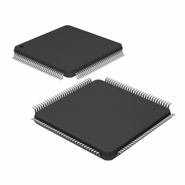
LQFP-120
PGA-299
Package
Document Number: 002-07917 Rev. *A
Page 3 of 64
�CY90920 Series
2. Pin Assignment
1
2
3
4
5
6
7
8
9
10
11
12
13
14
15
16
17
18
19
20
21
22
23
24
25
26
27
28
29
30
LQFP-120
90
89
88
87
86
85
84
83
82
81
80
79
78
77
76
75
74
73
72
71
70
69
68
67
66
65
64
63
62
61
RST
MD0
MD1
MD2
DVSS
DVCC
P87/PWM2M3
P86/PWM2P3
P85/PWM1M3
P84/PWM1P3
P83/PWM2M2
P82/PWM2P2
P81/PWM1M2
P80/PWM1P2
DVSS
DVCC
P77/PWM2M1
P76/PWM2P1
P75/PWM1M1
P74/PWM1P1
P73/PWM2M0
P72/PWM2P0
P71/PWM1M0
P70/PWM1P0
DVSS
DVCC
PE2/SGO1
P55/RX0/RX2/INT2
RSTO
P54/TX0/TX2/SGA1
P94/V0
P95/V1
P96/V2
V3
AVCC
AVRH
P50/INT0/ADTG
AVSS
P60/AN0
P61/AN1
P62/AN2
P63/AN3
P64/AN4
P65/AN5
P66/AN6
P67/AN7
VSS
PC0/SIN0/INT4
PC1/SOT0/INT5/IN3
PC2/SCK0/INT6/IN2
PC3/SIN1/INT7
PC4/SOT1
PC5/SCK1/TRG
PC6/PPG0/TOT1/IN7
PC7/PPG1/TIN1/IN6
PE0/TOT3
PE1/TIN3
P51/INT1/RX1/RX3
P52/TX1/TX3
P53/INT3
31
32
33
34
35
36
37
38
39
40
41
42
43
44
45
46
47
48
49
50
51
52
53
54
55
56
57
58
59
60
P30/SEG06
P31/SEG07
P32/SEG08
P33/SEG09
P34/SEG10
P35/SEG11
P36/SEG12
P37/SEG13
P40/SEG14
P41/SEG15
P42/SEG16
P43/SEG17
* P92/X0A
* P93/X1A
VCC
VSS
C
P44/SEG18
P45/SEG19
P46/SEG20
P47/SEG21
P90/SEG22
P91/SEG23
PD0/SIN2
PD1/SOT2
PD2/SCK2
PD3/SIN3
PD4/SOT3
PD5/SCK3
PD6/TOT2
120
119
118
117
116
115
114
113
112
111
110
109
108
107
106
105
104
103
102
101
100
99
98
97
96
95
94
93
92
91
P27/SEG05
P26/SEG04
P25/SEG03
P24/SEG02
P23/SEG01
P22/SEG00
COM3
COM2
COM1
COM0
P15/IN0
P14/TIN2/IN1
X0
X1
VSS
VCC
P13/PPG5
P12/TIN0/PPG4
P11/TOT0/PPG3/IN4
P10/PPG2/IN5
P07/SEG31
P06/SEG30
P05/SEG29
P04/SEG28
P03/SEG27
P02/SEG26
P01/SEG25
P00/SEG24
P57/SGA0
P56/SGO0/FRCK
(TOP VIEW)
(LQM120)
*: CY90V920-101, CY90F922NCS,CY90F923NCS,CY90F924NCS,CY90922NCS: P92, P93
CY90V920-102, CY90F922NC,CY90F923NC,CY90F924NC: X0A, X1A
Document Number: 002-07917 Rev. *A
Page 4 of 64
�CY90920 Series
3. Pin Descriptions
Pin No.
Pin Name
I/O Circuit
Type*1
108
X0
A
107
X1
13
X0A
P92
I
General-purpose I/O port
14
X1A
B
Low-speed oscillation output pin
P93
I
General-purpose I/O port
RST
C
Reset input pin
P00
F
90
93
P01
B
P02
F
P03
F
P04
F
P05
F
P06
F
P07
F
P10
F
I
104
I
General-purpose I/O port
TOT0
16-bit reload timer ch.0 TOT output pin
PPG3
16-bit PPG ch.3 output pin
P12
Input capture ch.4 trigger input pin
I
General-purpose I/O port
TIN0
16-bit reload timer ch.0 TIN input pin
PPG4
16-bit PPG ch.4 output pin
P13
I
PPG5
109
General-purpose I/O port
Input capture ch.5 trigger input pin
IN4
103
General-purpose I/O port
16-bit PPG ch.2 output pin
IN5
P11
General-purpose I/O port
LCD controller/driver segment output pin
PPG2
102
General-purpose I/O port
LCD controller/driver segment output pin
SEG31
101
General-purpose I/O port
LCD controller/driver segment output pin
SEG30
100
General-purpose I/O port
LCD controller/driver segment output pin
SEG29
99
General-purpose I/O port
LCD controller/driver segment output pin
SEG28
98
General-purpose I/O port
LCD controller/driver segment output pin
SEG27
97
General-purpose I/O port
LCD controller/driver segment output pin
SEG26
96
Low-speed oscillation input pin
LCD controller/driver segment output pin
SEG25
95
High-speed oscillation input pin
High-speed oscillation output pin
SEG24
94
Function
P14
General-purpose I/O port
16-bit PPG ch.5 output pin
I
General-purpose I/O port
TIN2
16-bit reload timer ch.2 TIN input pin
IN1
Input capture ch.1 trigger input pin
Document Number: 002-07917 Rev. *A
Page 5 of 64
�CY90920 Series
Pin No.
Pin Name
I/O Circuit
Type*1
110
P15
I
IN0
Function
General-purpose I/O port
Input capture ch.0 trigger input pin
111
COM0
P
LCD controller/driver common output pin
112
COM1
P
LCD controller/driver common output pin
113
COM2
P
LCD controller/driver common output pin
114
COM3
P
LCD controller/driver common output pin
115
P22
F
General-purpose I/O port
SEG00
116
P23
LCD controller/driver segment output pin
F
SEG01
117
P24
LCD controller/driver segment output pin
F
SEG02
118
P25
P26
P27
F
P30
P31
F
P32
P33
F
P34
P35
F
P36
P37
F
P40
P41
F
P42
SEG16
Document Number: 002-07917 Rev. *A
General-purpose I/O port
LCD controller/driver segment output pin
F
SEG15
11
General-purpose I/O port
LCD controller/driver segment output pin
SEG14
10
General-purpose I/O port
LCD controller/driver segment output pin
F
SEG13
9
General-purpose I/O port
LCD controller/driver segment output pin
SEG12
8
General-purpose I/O port
LCD controller/driver segment output pin
F
SEG11
7
General-purpose I/O port
LCD controller/driver segment output pin
SEG10
6
General-purpose I/O port
LCD controller/driver segment output pin
F
SEG09
5
General-purpose I/O port
LCD controller/driver segment output pin
SEG08
4
General-purpose I/O port
LCD controller/driver segment output pin
F
SEG07
3
General-purpose I/O port
LCD controller/driver segment output pin
SEG06
2
General-purpose I/O port
LCD controller/driver segment output pin
F
SEG05
1
General-purpose I/O port
LCD controller/driver segment output pin
SEG04
120
General-purpose I/O port
LCD controller/driver segment output pin
F
SEG03
119
General-purpose I/O port
General-purpose I/O port
LCD controller/driver segment output pin
F
General-purpose I/O port
LCD controller/driver segment output pin
Page 6 of 64
�CY90920 Series
Pin No.
Pin Name
I/O Circuit
Type*1
12
P43
F
SEG17
18
P44
P45
F
P46
P47
F
P50
I
INT0
59
P51
A/D converter external trigger input pin
I
INT1 external interrupt input pin
RX1
CAN interface 1 RX input pin
RX3
CAN interface 3 RX input pin
P52
I
P53
P54
CAN interface 3 TX output pin
I
92
I
CAN interface 0 TX output pin
TX2
CAN interface 2 TX output pin
P55
Sound generator ch.1 SGA output pin
I
General-purpose I/O port
RX0
CAN interface 0 RX input pin
RX2
CAN interface 2 RX input pin
INT2
INT2 external interrupt input pin
P56
I
General-purpose I/O port
SGO0
Sound generator ch.0 SGO output pin
FRCK
Free-run timer clock input pin
P57
I
P60
P61
AN1
Document Number: 002-07917 Rev. *A
General-purpose I/O port
Sound generator ch.0 SGA output pin
H
AN0
40
General-purpose I/O port
TX0
SGA0
39
General-purpose I/O port
INT3 external interrupt input pin
SGA1
91
General-purpose I/O port
CAN interface 1 TX output pin
INT3
63
General-purpose I/O port
INT1
TX3
61
General-purpose I/O port
INT0 external interrupt input pin
TX1
60
General-purpose I/O port
LCD controller/driver segment output pin
ADTG
58
General-purpose I/O port
LCD controller/driver segment output pin
F
SEG21
37
General-purpose I/O port
LCD controller/driver segment output pin
SEG20
21
General-purpose I/O port
LCD controller/driver segment output pin
F
SEG19
20
General-purpose I/O port
LCD controller/driver segment output pin
SEG18
19
Function
General-purpose I/O port
A/D converter input pin
H
General-purpose I/O port
A/D converter input pin
Page 7 of 64
�CY90920 Series
Pin No.
Pin Name
I/O Circuit
Type*1
41
P62
H
AN2
42
P63
P64
H
P65
P66
H
P67
P70
H
General-purpose I/O port
L
General-purpose output-only port
A/D converter input pin
PWM1P0
68
P71
Stepping motor controller ch.0 output pin
L
PWM1M0
69
P72
P73
P74
L
P75
P76
L
P77
P80
L
P81
P82
L
P83
P84
L
P85
PWM1M3
Document Number: 002-07917 Rev. *A
General-purpose output-only port
Stepping motor controller ch.2 output pin
L
PWM1P3
82
General-purpose output-only port
Stepping motor controller ch.2 output pin
PWM2M2
81
General-purpose output-only port
Stepping motor controller ch.2 output pin
L
PWM2P2
80
General-purpose output-only port
Stepping motor controller ch.2 output pin
PWM1M2
79
General-purpose output-only port
Stepping motor controller ch.1 output pin
L
PWM1P2
78
General-purpose output-only port
Stepping motor controller ch.1 output pin
PWM2M1
77
General-purpose output-only port
Stepping motor controller ch.1 output pin
L
PWM2P1
74
General-purpose output-only port
Stepping motor controller ch.1 output pin
PWM1M1
73
General-purpose output-only port
Stepping motor controller ch.0 output pin
L
PWM1P1
72
General-purpose output-only port
Stepping motor controller ch.0 output pin
PWM2M0
71
General-purpose output-only port
Stepping motor controller ch.0 output pin
L
PWM2P0
70
General-purpose I/O port
A/D converter input pin
AN7
67
General-purpose I/O port
A/D converter input pin
H
AN6
46
General-purpose I/O port
A/D converter input pin
AN5
45
General-purpose I/O port
A/D converter input pin
H
AN4
44
General-purpose I/O port
A/D converter input pin
AN3
43
Function
General-purpose output-only port
Stepping motor controller ch.3 output pin
L
General-purpose output-only port
Stepping motor controller ch.3 output pin
Page 8 of 64
�CY90920 Series
Pin No.
Pin Name
I/O Circuit
Type*1
83
P86
L
PWM2P3
84
P87
P90
L
P91
P94
F
P95
33
P96
G
49
50
51
52
54
General-purpose I/O port
LCD controller/driver reference power supply pin
V3
PC0
J
LCD controller/driver reference power supply pin
General-purpose I/O port
SIN0
UART ch.0 serial data input pin
INT4
INT4 external interrupt input pin
PC1
I
General-purpose I/O port
SOT0
UART ch.0 serial data output pin
INT5
INT5 external interrupt input pin
IN3
Input capture ch.3 trigger input pin
PC2
I
General-purpose I/O port
SCK0
UART ch.0 serial clock I/O pin
INT6
INT6 external interrupt input pin
IN2
Input capture ch.2 trigger input pin
PC3
J
General-purpose I/O port
SIN1
UART ch.1 serial data input pin
INT7
INT7 external interrupt input pin
PC4
I
SOT1
53
General-purpose I/O port
LCD controller/driver reference power supply pin
G
V2
48
General-purpose I/O port
LCD controller/driver reference power supply pin
V1
34
General-purpose I/O port
LCD controller/driver segment output pin
G
V0
32
General-purpose I/O port
LCD controller/driver segment output pin
SEG23
31
General-purpose output-only port
Stepping motor controller ch.3 output pin
F
SEG22
23
General-purpose output-only port
Stepping motor controller ch.3 output pin
PWM2M3
22
Function
PC5
General-purpose I/O port
UART ch.1 serial data output pin
I
General-purpose I/O port
SCK1
UART ch.1 serial clock I/O pin
TRG
16-bit PPG ch.0 to ch.5 external trigger input pin
PC6
I
General-purpose I/O port
PPG0
16-bit PPG ch.0 output pin
TOT1
16-bit reload timer ch.1 TOT output pin
IN7
Document Number: 002-07917 Rev. *A
Input capture ch.7 trigger input pin
Page 9 of 64
�CY90920 Series
Pin No.
Pin Name
I/O Circuit
Type*1
55
PC7
I
16-bit PPG ch.1 output pin
TIN1
16-bit reload timer ch.1 TIN input pin
PD0
Input capture ch.6 trigger input pin
J
SIN2
25
PD1
PD2
I
General-purpose I/O port
I
General-purpose I/O port
UART ch.2 serial data output pin
SCK2
27
PD3
UART ch.2 serial clock I/O pin
J
SIN3
28
PD4
PD5
PD6
I
General-purpose I/O port
I
General-purpose I/O port
UART ch.3 serial clock I/O pin
TOT2
56
PE0
16-bit reload timer ch.2 TOT output pin
I
General-purpose I/O port
I
General-purpose I/O port
TOT3
57
PE1
16-bit reload timer ch.3 TOT output pin
TIN3
64
PE2
General-purpose I/O port
UART ch.3 serial data output pin
SCK3
30
General-purpose I/O port
UART ch.3 serial data input pin
I
SOT3
29
General-purpose I/O port
UART ch.2 serial data input pin
SOT2
26
General-purpose I/O port
PPG1
IN6
24
Function
16-bit reload timer ch.3 TIN input pin
I
General-purpose I/O port
SGO1
Sound generator ch.1 SGO output pin
62
RSTO
N
Internal reset signal output pin
65, 75, 85
DVCC
Power supply input pins dedicated for high current output buffer
66, 76, 86
DVSS
Power supply GND pins dedicated for high current output buffer
35
AVCC
A/D converter dedicated power supply input pin
38
AVSS
A/D converter dedicated power supply GND pin
36
AVRH
A/D converter Vref+ input pin. Vref- is fixed to AVSS.
89
MD0
D
Mode setting input pin. Connect to VCC pin.
88
MD1
D
Mode setting input pin. Connect to VCC pin.
87
MD2
D/E*2
Mode setting input pin. Connect to VSS pin.
17
C
External capacitor pin.
Connect a 0.1 F capacitor between this pin and the VSS pin.
15, 105
VCC
Power supply input pins
16, 47, 106
VSS
GND power supply pins
*1: For I/O circuit type, refer to I/O Circuit Type.
*2: The I/O circuit type is D for Flash memory products and E for evaluation products.
Document Number: 002-07917 Rev. *A
Page 10 of 64
�CY90920 Series
4. I/O Circuit Type
Type
Circuit
Remarks
A
Oscillation circuit
High-speed oscillation feedback resistance:
approx. 1 M
X1
Xout
(Flash memory product/MASK ROM
product/Evaluation product)
X0
Standby control signal
B
Oscillation circuit
X1A
Low-speed oscillation feedback
resistance: approx. 10 M
Xout
X0A
Standby control signal
C
Input-only pin (with pull-up resistance)
Pull-up resistor
■
Attached pull-up resistor:
approx. 50 k
■
CMOS hysteresis input
(VIH/VIL 0.8 VCC/0.2 VCC)
CMOS hysteresis input
D
Input-only pin
■
CMOS hysteresis input
CMOS hysteresis input
(VIH/VIL 0.8 VCC/0.2 VCC)
Note:
The MD2 pin of the Flash memory products
uses this circuit type.
E
Input-only pin (with pull-down resistance)
CMOS hysteresis input
Pull-down resistor
■
Attached pull-down resistance:
approx. 50 k
■
CMOS hysteresis input
(VIH/VIL 0.8 VCC/0.2 VCC)
Note:
The MD2 pin of the evaluation products
uses this circuit type.
Document Number: 002-07917 Rev. *A
Page 11 of 64
�CY90920 Series
Type
Circuit
Remarks
F
LCD output common general-purpose port
P-ch
N-ch
■
CMOS output
(IOH/IOL 4 mA)
■
Hysteresis input
(VIH/VIL 0.8 VCC/0.2 VCC)
■
Automotive input
(VIH/VIL 0.8 VCC/0.5 VCC)
Pout
Nout
LCD input
CMOS hysteresis input
Standby control signal or LCD
input enable signal
Automotive input
Standby control signal or LCD
input enable signal
G
LCDC reference power supply common
general-purpose port
P-ch
N-ch
Pout
■
CMOS output (IOH/IOL 4 mA)
■
CMOS hysteresis input
(VIH/VIL 0.8 VCC/0.2 VCC)
■
Automotive input
(VIH/VIL 0.8 VCC/0.5 VCC)
Nout
LCDC reference power supply
input
CMOS hysteresis input
Standby control signal or
LCD output switching signal
Automotive input
Standby control signal or
LCD output switching signal
Document Number: 002-07917 Rev. *A
Page 12 of 64
�CY90920 Series
Type
Circuit
Remarks
H
A/D converter input common
general-purpose port
P-ch
Pout
N-ch
Nout
■
CMOS output
(IOH/IOL 4 mA)
■
CMOS hysteresis input
(VIH/VIL 0.8 VCC/0.2 VCC)
■
Automotive input
(VIH/VIL 0.8 VCC/0.5 VCC)
Analog input
CMOS hysteresis input
Standby control signal or
analog input enable signal
Automotive input
Standby control signal or
analog input enable signal
I
General-purpose port
■
CMOS output (IOH/IOL 4 mA)
P-ch
Pout
■
CMOS hysteresis input
(VIH/VIL 0.8 VCC/0.2 VCC)
N-ch
Nout
■
Automotive input
(VIH/VIL 0.8 VCC/0.5 VCC)
CMOS hysteresis input
Standby control signal
Automotive input
Standby control signal
J
General-purpose port (serial input)
P-ch
N-ch
Pout
Nout
CMOS hysteresis input
Standby control signal
■
CMOS output (IOH/IOL 4 mA)
■
CMOS hysteresis input
(VIH/VIL 0.8 VCC/0.2 VCC)
■
CMOS input (SIN)
(VIH/VIL 0.7 VCC/0.3 VCC)
■
Automotive input
(VIH/VIL 0.8 VCC/0.5 VCC)
Automotive input
Standby control signal
CMOS input (SIN)
Standby control signal
Document Number: 002-07917 Rev. *A
Page 13 of 64
�CY90920 Series
Type
Circuit
K
Remarks
A/D converter input common
general-purpose port (serial input)
P-ch
Pout
N-ch
Nout
Analog output
■
CMOS output (IOH/IOL 4 mA)
■
CMOS hysteresis input
(VIH/VIL 0.8 VCC/0.2 VCC)
■
CMOS input (SIN)
(VIH/VIL 0.7 VCC/0.3 VCC)
■
Automotive input
(VIH/VIL 0.8 VCC/0.5 VCC)
CMOS hysteresis input
Standby control signal or analog
input enable signal
Automotive input
Standby control signal or analog
input enable signal
CMOS input (SIN)
Standby control signal or analog
input enable signal
L
High current output port (SMC pin)
P-ch
Pout
High current
N-ch
Nout
M
CMOS output (IOH/IOL 30 mA)
LCDC output common general-purpose
port (serial input) )
P-ch
Pout
N-ch
Nout
■
CMOS output (IOH/IOL 4 mA)
■
CMOS hysteresis input
(VIH/VIL 0.8 VCC/0.2 VCC)
■
CMOS input (SIN)
(VIH/VIL 0.7 VCC/0.3 VCC)
■
Automotive input
(VIH/VIL 0.8 VCC/0.5 VCC)
LCDC output
CMOS hysteresis input
Standby control signal or
LCDC output switching signal
Automotive input
Standby control signal or
LCDC output switching signal
CMOS input (SIN)
Standby control signal or
LCDC output switching signal
Document Number: 002-07917 Rev. *A
Page 14 of 64
�CY90920 Series
Type
Circuit
Remarks
N
N-ch open-drain pin
Evaluation product
IOL 4 mA
Flash memory product
P-ch
Nout
N-ch
N-ch
O
Nout
Input-only pin
Automotive input
Automotive input
P
(VIH/VIL 0.8 VCC/0.5 VCC)
LCDC output pin (COM pin)
P-ch
LCDC output
N-ch
Document Number: 002-07917 Rev. *A
Page 15 of 64
�CY90920 Series
5. Handling Devices
Strictly Observe Maximum Rated Voltages (Preventing Latch-up)
In CMOS IC devices, a condition known as latch-up may occur if voltages higher than VCC or lower than VSS are applied to input or
output pins other than medium or high withstand voltage pins, or if the voltage applied between VCC and VSS pins exceeds the rated
voltage level. If a latch-up occurs, the power supply current may increase dramatically and may destroy semiconductor elements.
When using semiconductor devices, always take sufficient care to avoid exceeding maximum ratings.
When the analog system power supply is switched on or off, be careful not to apply the analog power supply (AVCC, AVRH), the
analog input voltages and the power supply voltage for the high current output buffer pins (DVCC) in excess of the digital power supply
voltage (VCC).
Once the digital power supply voltage (VCC) has been disconnected, the analog power supply (AVCC, AVRH) and the power supply
voltage for the high current output buffer pins (DVCC) may be turned on in any sequence.
Supply Voltage Stabilization
Rapid fluctuations in the power supply voltage can cause malfunctions even if the Vcc power supply voltage remains within the
warranted operating range. It is recommended that the power supply be stabilized such that ripple fluctuations (P-P value) at
commercial frequencies (50 Hz/60 Hz) be limited to within 10 of the standard VCC value, and that transient fluctuations due to power
supply switching, etc. be limited to a rate of 0.1 V/ms or less.
Precautions when Turning the Power On
In order to prevent the built-in step-down circuits from malfunctioning, the time taken for the voltage to rise (0.2 V to 2.7 V) during
power-on should be less than 50 s.
Handling Unused Pins
If unused input pins are left open, they may cause malfunctions or latch-up which may lead to permanent damage to the semiconductor. Unused input pins should therefore be pulled up or pulled down through a resistor of at least 2 k.
Unused input/output pins may be set to the output state and left open, or set to the input state and connected to a pull-up or pull-down
resistance of 2 k or more.
Handling A/D Converter Power Supply Pins
Even if the A/D converter is not used, the power supply pins should be connected such as AVCC VCC, and AVSS AVRH VSS.
Notes on Using an External Clock
Even when an external clock is used, an oscillation stabilization wait time is required following power-on reset or release from sub
clock mode or stop mode. Furthermore, only the X0A pin should be driven when an external clock is used, with the X1A pin open as
shown in the following diagram. Do not use high-speed oscillation pins (X0 and X1) for external clock input.
X0A
OPEN
X1A
CY90920 Series
Sample external clock connection
Notes on Operating in PLL Clock Mode
On this microcontroller, if in case the crystal oscillator breaks off or an external reference clock input stops while the PLL clock mode
is selected, a self-oscillator circuit contained in the PLL may continue its operation at its self-running frequency. However, Cypress
will not guarantee results of operations if such failure occurs.
Crystal Oscillator Circuit
Noise around the X0/X1, or X0A/X1A pins may cause this device to operate abnormally. In the interest of stable operation it is strongly
recommended that printed circuit artwork places ground bypass capacitors as close as possible to the X0/X1, X0A/X1A and crystal
oscillator (or ceramic oscillator) and that oscillator lines do not cross the lines of other circuits.
Please ask each crystal maker to evaluate the oscillational characteristics of the crystal and this device.
Document Number: 002-07917 Rev. *A
Page 16 of 64
�CY90920 Series
Power Supply Pins
Devices including multiple VCC or VSS pins are designed such that pins that need to be at the same potential are interconnected
internally to prevent malfunctions such as latch-up. To reduce unnecessary radiation, prevent malfunctioning of the strobe signal due
to the rise of ground level, and observe the standard for total output current, be sure to connect the VCC and VSS pins to the power
supply and ground externally.
Always connect all of the VCC pins to the same potential and all of the VSS pins to ground as shown in the following diagram. The
device will not operate correctly if multiple VCC or VSS pins are connected to different voltages, even if those voltages are within the
guaranteed operating ranges.
VCC
VSS
VCC
VSS
VSS
VCC
VCC
VSS
VSS
VCC
Power supply input pins (Vcc/Vss)
In addition, care must be given to connecting the VCC and VSS pins of this device to the current supply source with as low impedance
as possible. It is recommended that a 1.0 F bypass capacitor be connected between the VCC and VSS pins as close to the pins as
possible.
Sequence for Connecting the A/D Converter Power Supply and Analog Inputs
The A/D converter power supply (AVCC, AVRH) and analog inputs (AN0 to AN7) must be applied after the digital power supply (VCC)
is switched on. When turning the power off, the A/D converter power supply and analog inputs must be disconnected before the digital
power supply is switched off (VCC). Ensure that AVRH does not exceed AVcc during either power-on or power-off. Even when pins
which double as analog input pins are used as input ports, be sure that the input voltage does not exceed AVCC (turning on/off the
analog and digital power supplies simultaneously is acceptable).
Handling the Power Supply for High-current Output Buffer Pins (DVCC, DVSS)
■
Flash memory products and MASK ROM products (CY90F922NC/F922NCS/922NCS/F923NC/F923NCS/F924NC/F924NCS)
In the Flash memory products and MASK ROM products, the power supply for the high-current output buffer pins (DVCC, DVSS)
is isolated from the digital power supply (VCC).
Therefore, DVcc can therefore be set to a higher voltage than Vcc. If the power supply for the high-current output buffer pins (DVCC,
DVSS) is supplied before the digital power supply (VCC), however, care needs to be taken because it is possible that the port 7 or
port 8 stepping motor outputs may momentarily output an “H” or “L” level. In order to prevent this, connect the digital power supply
(VCC) prior to connecting the power supply for the high-current output buffer pins. Even when the high-current output buffer pins
are used as general-purpose ports, power should be supplied to the power supply pins for the high-current output buffer pins
(DVCC, DVSS).
■
Evaluation product (CY90V920-101/CY90V920-102)
In the evaluation products, the power supply for the high-current output buffer pins (DVCC, DVSS) is not isolated from the digital
power supply (VCC). Therefore, DVCC must therefore be set to a lower voltage than Vcc. The power supply for the high-current
output buffer pins (DVCC, DVSS) must always be applied after the digital power supply (VCC) has been connected, and disconnected before the digital power supply (Vcc) is disconnected (the power supply for the high-current output buffer pins may also be
connected and disconnected simultaneously with the digital power supply).
Even when the high-current output buffer pins are used as general-purpose ports, power should be supplied to the power supply
pins for the high-current output buffer pins (DVCC, DVSS).
Document Number: 002-07917 Rev. *A
Page 17 of 64
�CY90920 Series
Pull-up/Pull-down Resistors
CY90920 series does not support internal pull-up/pull-down resistors. Use external components as necessary.
Precautions When Not Using a Sub Clock Signal
If the X0A and X1A pins are not connected to an oscillator, apply a pull-down resistance to the X0A pin and leave the X1A pin open.
Notes on Operating When the External Clock is Stopped
The CY90920 series is not guaranteed to operate correctly using the internal oscillator circuit when there is no external oscillator or
the external clock input is stopped.
Flash Memory Security Function
A security bit is located within the Flash memory region. The security function is activated by writing the protection code 01H to the
security bit.
Do not write the value 01H to this address if you are not using the security function.
Please refer to following table for the address of the security bit.
Flash Memory Size
Address for Security Bit
CY90F922NC
CY90F922NCS
Built-in 2 Mbits Flash Memory
FC0001H
CY90F923NCS
Built-in 3 Mbits Flash Memory
F80001H
CY90F924NCS
Built-in 4 Mbits Flash Memory
F80001H
Serial Communication
In serial communication, reception of wrong data may occur due to noise or other causes. Therefore, design a printed circuit board
to prevent noise from occurring. Taking account of the reception of wrong data, detect errors by measures such as adding a checksum
to the end of data. If an error is detected, retransmit the data.
Characteristic Difference Between Flash Device and MASK ROM Device
In the flash device and the MASK ROM device, the electrical characteristic including current consumption, ESD, latch-up, the noise
characteristic, and oscillation characteristic, etc. is different according to the difference between the chip layout and the memory
structure.
Reconfirm the electrical characteristic when the product is replaced by another product of the same series.
Document Number: 002-07917 Rev. *A
Page 18 of 64
�CY90920 Series
6. Block Diagram
CPU
F2MC-16LX core
Clock control circuit
Watchdog timer
Time-base timer
Watch timer
(for sub clock)
Interrupt controller
Low-voltage reset
Sound generator 0
Sound generator 1
CPU operation
detection reset
CAN controller 0
CAN controller 1
CAN controller 2
CAN controller 3
External interrupt
(8 channels)
Stepping motor controller 0
Stepping motor controller 1
LIN-UART 0
Prescaler 0
LIN-UART 1
Prescaler 1
LIN-UART 2
Prescaler 2
LIN-UART 3
Prescaler 3
Stepping motor controller 2
F2MC-16LX BUS
Stepping motor controller 3
16-bit PPG timer 0
16-bit PPG timer 1
16-bit PPG timer 2
16-bit PPG timer 3
16-bit PPG timer 4
16-bit PPG timer 5
A/D converter
(8 channels)
LCD controller/driver
(32 SEG/4 COM)
RAM
ROM/Flash
16-bit reload timer 0
16-bit reload timer 1
16-bit reload timer 2
16-bit reload timer 3
Tool interface
Real-time watch timer
(main)
16-bit ICU 0 (2 channels)
16-bit ICU 1 (2 channels)
16-bit ICU 2 (2 channels)
16-bit ICU 3 (2 channels)
16-bit free-run timer
: Flash memory product and MASK ROM product only
: Evaluation product only
Document Number: 002-07917 Rev. *A
Page 19 of 64
�CY90920 Series
7. Memory Map
000000 H
000000 H
Peripheral area
0000F0H
Peripheral area
0000EFH
000100 H
Register
RAM area
(13.5 Kbytes)
003700 H
000100 H
Register
RAM area
Address #3
003700 H
Peripheral area
004000 H
Peripheral area
004000 H
RAM area
(16 Kbytes)
008000 H
RAM area
Address #2
008000 H
ROM area
(FF bank image)
ROM area
(FF bank image)
010000 H
010000 H
F80000 H
Address #1
ROM area*
FFFFFF H
ROM area*
: Internal access
: Internal access prohibited
FFFFFF H
CY90F922 / CY90922
CY90F923 / CY90F924
CY90V220 (Evaluation product)
ROM (Flash)
Capacitance
RAM Capacitance
Address #1
Address #2
Address #3
CY90F922NC/F922NCS/922NCS
256 Kbytes
10 Kbytes
FC0000H
004000H
002900H
CY90F923NC/F923NCS
384 Kbytes
16 Kbytes
FA0000H
004A00H
003700H
CY90F924NC/F924NCS
512 Kbytes
24 Kbytes
F80000H
006A00H
003700H
Parts No.
*:Evaluation products do not contain internal ROM. Treat this address as the ROM decode area used by the tools.
Note:
To select models without the ROM mirror function, refer to the “ROM Mirror Function Selection Module” in Hardware Manual. The
image of the ROM data in the FF bank appears at the top of the 00 bank, in order to enable efficient use of small C compiler models.
The lower 16-bits of the FF bank addresses are allocated to the same addresses as the lower 16-bits of the 00 bank, making it
possible to reference tables in ROM without declaring the “far” modifier with the pointers. For example, when an access is made
to the address 00C000H, the actual address to be accessed is FFC000H in ROM. Because the size of the FF bank ROM area
exceeds 32 Kbytes, it is not possible to view the entire region in the 00 bank image. Therefore because the ROM data from FF8000H
to FFFFFFH appears in the image from 008000H to 00FFFFH, it is recommended that ROM data tables be stored in the area from
FF8000H to FFFFFFH.
Document Number: 002-07917 Rev. *A
Page 20 of 64
�CY90920 Series
8. I/O Map
Address
Register Name
Symbol
Read/Write
Resource Name
Initial Value
000000H Port 0 data register
PDR0
R/W
Port 0
XXXXXXXXB
000001H Port 1 data register
PDR1
R/W
Port 1
XXXXXXXXB
000002H Port 2 data register
PDR2
R/W
Port 2
XXXXXXXXB
000003H Port 3 data register
PDR3
R/W
Port 3
XXXXXXXXB
000004H Port 4 data register
PDR4
R/W
Port 4
XXXXXXXXB
000005H Port 5 data register
PDR5
R/W
Port 5
XXXXXXXXB
000006H Port 6 data register
PDR6
R/W
Port 6
XXXXXXXXB
000007H Port 7 data register
PDR7
R/W
Port 7
XXXXXXXXB
000008H Port 8 data register
PDR8
R/W
Port 8
XXXXXXXXB
000009H Port 9 data register
PDR9
R/W
Port 9
XXXXXXXXB
R/W
Port C
XXXXXXXXB
00000AH,
00000BH
(Disabled)
00000CH Port C data register
PDRC
00000DH Port D data register
PDRD
R/W
Port D
XXXXXXXXB
00000EH Port E data register
PDRE
R/W
Port E
XXXXXXXXB
00000FH
(Disabled)
000010H Port 0 direction register
DDR0
R/W
Port 0
00000000B
000011H
Port 1 direction register
DDR1
R/W
Port 1
XX000000B
000012H Port 2 direction register
DDR2
R/W
Port 2
000000XXB
000013H Port 3 direction register
DDR3
R/W
Port 3
00000000B
000014H Port 4 direction register
DDR4
R/W
Port 4
00000000B
000015H Port 5 direction register
DDR5
R/W
Port 5
00000000B
000016H Port 6 direction register
DDR6
R/W
Port 6
00000000B
000017H Port 7 direction register
DDR7
R/W
Port 7
00000000B
000018H Port 8 direction register
DDR8
R/W
Port 8
00000000B
000019H Port 9 direction register
DDR9
R/W
Port 9
X0000000B
00001AH Analog input enable
ADER6
R/W
Port 6, A/D
11111111B
R/W
Port C
00000000B
00001BH
(Disabled)
00001CH Port C direction register
DDRC
00001DH Port D direction register
DDRD
R/W
Port D
X0000000B
00001EH Port E direction register
DDRE
R/W
Port E
XXXXX000B
ADCS0
R/W
A/D converter
000XXXX0B
000021H Higher A/D control status register
ADCS1
R/W
0000000XB
000022H Lower A/D control status register
ADCR0
R
00000000B
000023H Higher A/D data register
ADCR1
R
XXXXXX00B
00001FH
000020H Lower A/D control status register
Document Number: 002-07917 Rev. *A
(Disabled)
Page 21 of 64
�CY90920 Series
Address
Register Name
000024H Compare clear register
Symbol
Read/Write
Resource Name
Initial Value
CPCLR
R/W
16-bit
free-run timer
XXXXXXXXB
000025H
R/W
000026H Timer data register
TCDT
000027H
XXXXXXXXB
R/W
00000000B
R/W
00000000B
000028H Lower timer control status register
TCCSL
R/W
00000000B
000029H Higher timer control status register
TCCSH
R/W
01-00000B
00002AH Lower PPG0 control status register
PCNTL0
R/W
00002BH Higher PPG0 control status register
PCNTH0
R/W
00002CH Lower PPG1 control status register
PCNTL1
R/W
00002DH Higher PPG1 control status register
PCNTH1
R/W
00002EH Lower PPG2 control status register
PCNTL2
R/W
00002FH Higher PPG2 control status register
PCNTH2
R/W
000030H External interrupt enable
ENIR
R/W
000031H External interrupt request
EIRR
R/W
16-bit PPG0
00000000B
00000001B
16-bit PPG1
00000000B
00000001B
16-bit PPG2
00000000B
00000001B
External interrupt
00000000B
00000000B
000032H Lower external interrupt level
ELVRL
R/W
00000000B
000033H Higher external interrupt level
ELVRH
R/W
00000000B
000034H Serial mode register 0
SMR0
R/W, W
000035H Serial control register 0
SCR0
R/W, W
000036H Reception/transmission data register 1
RDR0/
TDR0
R/W
00000000B
000037H Serial status register 0
SSR0
R/W, R
00001000B
000038H Extended communication control register 0
ECCR0
R/W, R
000000XXB
000039H Extended status control register 0
ESCR0
R/W
00000100B
00003AH Baud rate generator register 00
BGR00
R/W
00000000B
00003BH Baud rate generator register 01
BGR01
R/W, R
00000000B
UART
(LIN/SCI) 0
00003CH
to
00003FH
(Disabled)
000040H to
00004FH
Area reserved for CAN Controller 0. Refer to CAN Controllers
00000000B
00000000B
000050H Lower timer control status register 0
TMCSR0L
R/W
000051H Higher timer control status register 0
TMCSR0H
R/W
XXX10000B
TMR0/
TMRLR0
R/W
XXXXXXXXB
000054H Lower timer control status register 1
TMCSR1L
R/W
000055H Higher timer control status register 1
TMCSR1H
R/W
XXX10000B
TMR1/
TMRLR1
R/W
XXXXXXXXB
000052H Timer register 0/reload register 0
000053H
000056H Timer register 1/reload register 1
000057H
00000000B
XXXXXXXXB
16-bit reload timer 1
00000000B
XXXXXXXXB
000058H LCD output control register 1
LOCR1
R/W
000059H LCD output control register 2
LOCR2
R/W
Document Number: 002-07917 Rev. *A
16-bit reload timer 0
LCDC
11111111B
00000000B
Page 22 of 64
�CY90920 Series
Address
Register Name
Symbol
Read/Write
Resource Name
Initial Value
00005AH Lower sound control register 0
SGCRL0
R/W
Sound generator 0
00000000B
00005BH Higher sound control register 0
SGCRH0
R/W
0XXXX100B
00005CH Frequency data register 0
SGFR0
R/W
XXXXXXXXB
00005DH Amplitude data register 0
SGAR0
R/W
00000000B
00005EH Decrement grade register 0
SGDR0
R/W
XXXXXXXXB
00005FH Tone count register 0
SGTR0
R/W
XXXXXXXXB
000060H Input capture register 0
IPCP0
R
Input capture 0/1
000061H
XXXXXXXXB
XXXXXXXXB
000062H Input capture register 1
IPCP1
R
XXXXXXXXB
000063H
XXXXXXXXB
000064H Input capture register 2
IPCP2
R
Input capture 2/3
000065H
XXXXXXXXB
XXXXXXXXB
000066H Input capture register 3
IPCP3
R
XXXXXXXXB
000067H
XXXXXXXXB
000068H Input capture control status 0/1
ICS01
R/W
000069H Input capture edge register 0/1
ICE01
R/W
00006AH Input capture control status 2/3
ICS23
R/W
00006BH Input capture edge register 2/3
ICE23
R/W
Input capture 0/1
00000000B
XXX0X0XXB
Input capture 2/3
00000000B
XXXXXXXXB
00006CH Lower LCD control register
LCRL
R/W
00006DH Higher LCD control register
LCRH
R/W
00006EH Low voltage/CPU operation detection reset
control register
LVRC
R/W
Low voltage/CPU
operation
detection reset
00111000B
00006FH ROM mirror
ROMM
W
ROM mirror
XXXXXXX1B
000070H to
00007FH
LCD controller/
driver
00010000B
00000000B
Area reserved for CAN Controller 1. Refer to CAN Controllers
000080H PWM control register 0
000081H
000082H PWM control register 1
000083H
000084H PWM control register 2
000085H
000086H PWM control register 3
000087H
000088H LCD output control register 3
000089H
PWC0
R/W
Stepping motor
controller 0
000000X0B
R/W
Stepping motor
controller 1
000000X0B
R/W
Stepping motor
controller 2
000000X0B
R/W
Stepping motor
controller 3
000000X0B
R/W
LCDC
XXXXX111B
A/D converter
00000000B
(Disabled)
PWC1
(Disabled)
PWC2
(Disabled)
PWC3
(Disabled)
LOCR3
(Disabled)
00008AH A/D setting register 0
ADSR0
R/W
00008BH A/D setting register 1
ADSR1
R/W
Document Number: 002-07917 Rev. *A
00000000B
Page 23 of 64
�CY90920 Series
Address
Register Name
Symbol
Read/Write
Resource Name
Initial Value
00008CH Port input level select 0
PIL0
R/W
00000000B
00008DH Port input level select 1
PIL1
R/W
Port input level
select
00008EH Port input level select 2
PIL2
R/W
00008FH to
00009DH
XXXX0000B
XXXX0000B
(Disabled)
00009EH Program address detection control register
PACSR
R/W
Address match
detection
XXXX0X0XB
00009FH Delayed Interrupt/Release Register
DIRR
R/W
Delay interrupt
XXXXXXX0B
0000A0H Power saving mode control register
LPMCR
R/W
CKSCR
R/W, R
Power saving
control circuit
00011000B
0000A1H Clock select register
R, W
Watchdog timer
XXXXX111B
0000A2H
to
0000A7H
11111100B
(Disabled)
0000A8H Watchdog timer control register
WDTC
0000A9H Time-base timer control register
TBTC
R/W, W
Time-base timer
1XX00100B
0000AAH Watch timer control register
WTC
R/W, W, R
Watch timer
(sub clock)
10001000B
0000ABH
to
0000ADH
(Disabled)
0000AEH Flash memory control status register
FMCS
R/W
Flash interface
000X0000B
0000B0H Interrupt control register 00
ICR00
R/W
Interrupt controller
00000111B
0000B1H Interrupt control register 01
ICR01
R/W
00000111B
0000B2H Interrupt control register 02
ICR02
R/W
00000111B
0000B3H Interrupt control register 03
ICR03
R/W
00000111B
0000B4H Interrupt control register 04
ICR04
R/W
00000111B
0000B5H Interrupt control register 05
ICR05
R/W
00000111B
0000B6H Interrupt control register 06
ICR06
R/W
00000111B
0000B7H Interrupt control register 07
ICR07
R/W
00000111B
0000B8H Interrupt control register 08
ICR08
R/W
00000111B
0000AFH
(Disabled)
0000B9H Interrupt control register 09
ICR09
R/W
00000111B
0000BAH Interrupt control register 10
ICR10
R/W
00000111B
0000BBH Interrupt control register 11
ICR11
R/W
00000111B
0000BCH Interrupt control register 12
ICR12
R/W
00000111B
0000BDH Interrupt control register 13
ICR13
R/W
00000111B
0000BEH Interrupt control register 14
ICR14
R/W
00000111B
0000BFH Interrupt control register 15
ICR15
R/W
00000111B
0000C0H
to
0000C3H
Document Number: 002-07917 Rev. *A
(Disabled)
Page 24 of 64
�CY90920 Series
Address
Register Name
Symbol
Read/Write
Resource Name
Initial Value
0000C4H Serial mode register 1
SMR1
R/W, W
00000000B
0000C5H Serial control register 1
SCR1
R/W, W
UART
(LIN/SCI) 1
0000C6H Reception/transmission data register 1
00000000B
RDR1/TDR1
R/W
00000000B
SSR1
R/W, R
00001000B
0000C8H Extended communication control register 1
ECCR1
R/W, R
000000XXB
0000C9H Extended status control register 1
ESCR1
R/W
00000100B
0000CAH Baud rate generator register 10
BGR10
R/W
00000000B
0000CBH Baud rate generator register 11
BGR11
R/W, R
00000000B
0000CCH Lower watch timer control register
WTCRL
R/W
0000CDH Middle watch timer control register
WTCRM
R/W
0000CEH Higher watch timer control register
WTCRH
R/W
0000CFH Sub clock control register
PSCCR
W
Sub clock
XXXX0000B
0000D0H Input capture control status 4/5
ICS45
R/W
Input capture 4/5
00000000B
0000D1H Input capture edge register 4/5
ICE45
R/W, R
0000C7H Serial status register 1
0000D2H Input capture control status 6/7
ICS67
R/W
0000D3H Input capture edge register 6/7
ICE67
R/W, R
0000D4H Lower timer control status register 2
TMCSR2L
R/W
0000D5H Higher timer control status register 2
TMCSR2H
R/W
0000D6H Lower timer control status register 3
TMCSR3L
R/W
0000D7H Higher timer control status register 3
TMCSR3H
R/W
0000D8H Lower sound control register 1
SGCRL1
R/W
0000D9H Higher sound control register 1
SGCRH1
R/W
0000DAH Lower PPG3 control status register
PCNTL3
R/W
0000DBH Higher PPG3 control status register
PCNTH3
R/W
0000DCH Lower PPG4 control status register
PCNTL4
R/W
0000DDH Higher PPG4 control status register
PCNTH4
R/W
0000DEH Lower PPG5 control status register
PCNTL5
R/W
0000DFH Higher PPG5 control status register
PCNTH5
R/W
0000E0H Serial mode register 2
SMR2
R/W, W
0000E1H Serial control register 2
SCR2
R/W, W
0000E2H Reception/transmission data register 2
Real-time
watch timer
000XXXX0B
00000000B
XXXXXX00B
XXXXXXXXB
Input capture 6/7
00000000B
XXX0X0XXB
16-bit
reload timer 2
16-bit
reload timer 3
Sound generator 1
00000000B
XXX10000B
00000000B
XXX10000B
00000000B
0XXXX100B
16-bit PPG3
00000000B
00000001B
16-bit PPG4
00000000B
00000001B
16-bit PPG5
00000000B
00000001B
UART
(LIN/SCI) 2
00000000B
00000000B
RDR2/TDR2
R/W
00000000B
SSR2
R/W, R
00001000B
0000E4H Extended communication control register 2
ECCR2
R/W, R
000000XXB
0000E5H Extended status control register 2
ESCR2
R/W
00000100B
0000E6H Baud rate generator register 20
BGR20
R/W
00000000B
0000E7H Baud rate generator register 21
BGR21
R/W, R
00000000B
0000E3H Serial status register 2
Document Number: 002-07917 Rev. *A
Page 25 of 64
�CY90920 Series
Address
Register Name
Symbol
Read/Write
Resource Name
Initial Value
0000E8H Serial mode register 3
SMR3
R/W, W
00000000B
0000E9H Serial control register 3
SCR3
R/W, W
UART
(LIN/SCI) 3
0000EAH Reception/transmission data register 3
00000000B
RDR3/TDR3
R/W
00000000B
SSR3
R/W, R
00001000B
0000ECH Extended communication control register 3
ECCR3
R/W, R
000000XXB
0000EDH Extended status control register 3
ESCR3
R/W
00000100B
0000EEH Baud rate generator register 30
BGR30
R/W
00000000B
0000EFH Baud rate generator register 31
BGR31
R/W, R
00000000B
001FF0H Program address detection register 0
PADR0
R/W
001FF1H Program address detection register 1
PADR0
R/W
001FF2H Program address detection register 2
PADR0
R/W
XXXXXXXXB
001FF3H Program address detection register 3
PADR1
R/W
XXXXXXXXB
001FF4H Program address detection register 4
PADR1
R/W
XXXXXXXXB
001FF5H Program address detection register 5
PADR1
R/W
XXXXXXXXB
0000EBH Serial status register 3
Address match
detection
003700H to
0037FFH
Area reserved for CAN Controller 2. Refer to CAN Controllers
003800H to
0038FFH
Area reserved for CAN Controller 3. Refer to CAN Controllers
003900H to
00391FH
(Disabled)
003920H PPG0 down counter register
PDCR0
R
16-bit PPG0
003921H
003922H PPG0 cycle setting register
PCSR0
W
003927H
003928H PPG1 down counter register
PDUT0
W
11111111B
16-bit PPG0
PPGDIV0
R/W, R
R
00392FH
Document Number: 002-07917 Rev. *A
16-bit PPG1
11111111B
11111111B
PCSR1
W
11111111B
PDUT1
W
00000000B
11111111B
00392DH
00392EH PPG1output division setting register
11111100B
(Disabled)
PDCR1
00392BH
00392CH PPG1 duty setting register
00000000B
00000000B
003929H
00392AH PPG1 cycle setting register
11111111B
11111111B
003925H
003926H PPG0 output division setting register
XXXXXXXXB
11111111B
003923H
003924H PPG0 duty setting register
XXXXXXXXB
00000000B
PPGDIV1
R/W, R
11111100B
(Disabled)
Page 26 of 64
�CY90920 Series
Address
Register Name
003930H PPG2 down counter register
Symbol
Read/Write
Resource Name
Initial Value
PDCR2
R
16-bit PPG2
11111111B
003931H
003932H PPG2 cycle setting register
11111111B
PCSR2
W
11111111B
003933H
003934H PPG2 duty setting register
11111111B
PDUT2
W
00000000B
003935H
003936H PPG2 output division setting register
003937H to
00393FH
003940H Input capture register 4
00000000B
PPGDIV2
R/W, R
11111100B
(Disabled)
IPCP4
R
Input capture 4/5
003941H
003942H Input capture register 5
IPCP5
R
XXXXXXXXB
003943H
003944H Input capture register 6
XXXXXXXXB
IPCP6
R
Input capture 6/7
003945H
003946H Input capture register 7
003950H Minute data register 2/Reload register 2
003951H
003952H Minute data register 3/Reload register 3
003953H
003954H to
003957H
003958H Sub second data register
XXXXXXXXB
XXXXXXXXB
IPCP7
R
XXXXXXXXB
003947H
003948H to
00394FH
XXXXXXXXB
XXXXXXXXB
XXXXXXXXB
(Disabled)
TMR2/
TMRLR2
R/W
16-bit reload timer 2
TMR3/
TMRLR3
R/W
16-bit reload timer 3
XXXXXXXXB
XXXXXXXXB
XXXXXXXXB
XXXXXXXXB
(Disabled)
WTBR
R/W
003959H
00395AH
Real time
watch timer
XXXXXXXXB
XXXXXXXXB
XXXXXXXXB
00395BH Second data register
WTSR
R/W
XX000000B
00395CH Minute data register
WTMR
R/W
XX000000B
00395DH Hour data register
WTHR
R/W
XXX00000B
00395EH Day data register
WTDR
R/W
00X00001B
00395FH
Document Number: 002-07917 Rev. *A
(Disabled)
Page 27 of 64
�CY90920 Series
Address
Register Name
003960H LCD display RAM
Symbol
Read/Write
Resource Name
Initial Value
VRAM
R/W
LCD
controller/driver
XXXXXXXXB
003961H
XXXXXXXXB
003962H
XXXXXXXXB
003963H
XXXXXXXXB
003964H
XXXXXXXXB
003965H
XXXXXXXXB
003966H
XXXXXXXXB
003967H
XXXXXXXXB
003968H
XXXXXXXXB
003969H
XXXXXXXXB
00396AH
XXXXXXXXB
00396BH
XXXXXXXXB
00396CH
XXXXXXXXB
00396DH
XXXXXXXXB
00396EH
XXXXXXXXB
00396FH
XXXXXXXXB
003970H to
003973H
(Disabled)
003974H Frequency data register 1
SGFR1
R/W
003975H Amplitude data register 1
SGAR1
R/W
00000000B
003976H Decrement grade register 1
SGDR1
R/W
XXXXXXXXB
003977H Tone count register 1
SGTR1
R/W
XXXXXXXXB
003978H to
00397FH
003980H PWM1 compare register 0
XXXXXXXXB
(Disabled)
PWC10
R/W
003981H
003982H PWM2 compare register 0
Sound generator 1
PWC20
Stepping motor
controller 0
R/W
XXXXXXXXB
XXXXXXXXB
XXXXXXXXB
003983H
XXXXXXXXB
003984H PWM1 select register 0
PWS10
R/W
00000000B
003985H PWM2 select register 0
PWS20
R/W
X0000000B
003986H,
003987H
003988H PWM1 compare register 1
(Disabled)
PWC11
R/W
003989H
00398AH PWM2 compare register 1
Stepping motor
controller 1
XXXXXXXXB
XXXXXXXXB
PWC21
R/W
00398CH PWM1 select register 1
PWS11
R/W
00000000B
00398DH PWM2 select register 1
PWS21
R/W
X0000000B
00398BH
00398EH,
00398FH
Document Number: 002-07917 Rev. *A
XXXXXXXXB
XXXXXXXXB
(Disabled)
Page 28 of 64
�CY90920 Series
Address
Register Name
003990H PWM1 compare register 2
Symbol
Read/Write
Resource Name
Initial Value
PWC12
R/W
Stepping motor
controller 2
XXXXXXXXB
003991H
003992H PWM2 compare register 2
PWC22
R/W
XXXXXXXXB
XXXXXXXXB
003993H
XXXXXXXXB
003994H PWM1 select register 2
PWS12
R/W
00000000B
003995H PWM2 select register 2
PWS22
R/W
X0000000B
003996H,
003997H
(Disabled)
003998H PWM1 compare register 3
PWC13
R/W
PWC23
R/W
003999H
00399AH PWM2 compare register 3
Stepping motor
controller 3
XXXXXXXXB
XXXXXXXXB
XXXXXXXXB
00399BH
XXXXXXXXB
00399CH PWM1 select register 3
PWS13
R/W
00000000B
00399DH PWM2 select register 3
PWS23
R/W
X0000000B
00399EH
to
0039A5H
(Disabled)
0039A6H Flash write control register 0
FWR0
0039A7H Flash write control register 1
FWR1
R/W
Flash I/F
0039A8H
to
0039BFH
(Disabled)
0039C0H
to
0039DFH
Area reserved for CAN Controller 2. Refer to CAN Controllers
0039E0H
to
0039FFH
Area reserved for CAN Controller 3. Refer to CAN Controllers
003A00H
to
003AFFH
Area reserved for CAN Controller 0. Refer to CAN Controllers
003B00H
to
003BFFH
Area reserved for CAN Controller 1. Refer to CAN Controllers
003C00H
to
003CFFH
Area reserved for CAN Controller 0. Refer to CAN Controllers
003D00H
to
003DFFH
Area reserved for CAN Controller 1. Refer to CAN Controllers
003E00H
to
003EFFH
Area reserved for CAN Controller 2. Refer to CAN Controllers
003F00H to
003FFFH
Area reserved for CAN Controller 3. Refer to CAN Controllers
Document Number: 002-07917 Rev. *A
00000000B
00000000B
Page 29 of 64
�CY90920 Series
9. CAN Controllers
The CAN controller has the following features :
■
Conforms to CAN Specification Version 2.0 Part A and B
❐ Supports transmission/reception in standard frame and extended frame formats
■
Supports transmission of data frames by receiving remote frames
■
16 transmission/reception message buffers
❐ 29-bit ID and 8-byte data
❐ Multi-level message buffer configuration
■
Provides full-bit comparison, full-bit mask, acceptance register 0/acceptance register 1 for each message buffer as ID acceptance
mask
❐ 2 acceptance mask registers in either standard frame format or extended frame formats
■
Bit rate programmable from 10 kbps to 2 Mbps (when input clock is at 16 MHz)
Table 9-1. List of Control Registers(1)
Address
Abbreviation
Access
Initial Value
CSR
R/W, R
00---000B
0----0-1B
LEIR
R/W
003E03H
003F02H Last event indicator
register
003F03H
--------B
000-0000B
003D04H
003E04H
003F04H RX/TX error counter
RTEC
R
003C05H
003D05H
003E05H
003F05H
00000000B
00000000B
003C06H
003D06H
003E06H
003F06H Bit timing register
BTR
R/W
003C07H
003D07H
003E07H
003F07H
-1111111B
11111111B
Abbreviation
Access
Initial Value
BVALR
R/W
00000000B
00000000B
TREQR
R/W
00000000B
00000000B
TCANR
W
00000000B
00000000B
TCR
R/W
00000000B
00000000B
RCR
R/W
00000000B
00000000B
RRTRR
R/W
00000000B
00000000B
ROVRR
R/W
00000000B
00000000B
CAN3
Register
CAN0
CAN1
CAN2
003C00H
003D00H
003E00H
003F00H Control status register
003C01H
003D01H
003E01H
003F01H
003C02H
003D02H
003E02H
003C03H
003D03H
003C04H
Table 9-2. List of Control Registers(2)
Address
CAN3
Register
CAN0
CAN1
CAN2
000040H
000070H
0039C0H
0039D0H Message buffer valid register
000041H
000071H
0039C1H
0039D1H
000042H
000072H
0039C2H
0039D2H Transmit request register
000043H
000073H
0039C3H
0039D3H
000044H
000074H
0039C4H
0039D4H Transmit cancel register
000045H
000075H
0039C5H
0039D5H
000046H
000076H
0039C6H
0039D6H Transmit complete register
000047H
000077H
0039C7H
0039D7H
000048H
000078H
0039C8H
0039D8H Receive complete register
000049H
000079H
0039C9H
0039D9H
00004AH
00007AH
0039CAH
0039DAH Remote request receive register
00004BH
00007BH
0039CBH
0039DBH
00004CH
00007CH
0039CCH
0039DCH Receive overrun register
00004DH
00007DH
0039CDH
0039DDH
Document Number: 002-07917 Rev. *A
Page 30 of 64
�CY90920 Series
Address
Register
CAN0
CAN1
CAN2
CAN3
00004EH
00007EH
0039CEH
0039DEH Receive interrupt enable register
00004FH
00007FH
0039CFH
0039DFH
003C08H
003D08H
003E08H
003F08H IDE register
003C09H
003D09H
003E09H
003F09H
003C0AH
003D0AH
003E0AH
003F0AH Transmit RTR register
Abbreviation
Access
Initial Value
RIER
R/W
00000000B
00000000B
IDER
R/W
XXXXXXXXB
XXXXXXXXB
003C0BH
003D0BH
003E0BH
003F0BH
003C0CH
003D0CH
003E0CH
003C0DH
003D0DH
003E0DH
003F0CH Remote frame receive wait
register
003F0DH
003C0EH
003D0EH
003E0EH
003F0EH Transmit interrupt enable register
003C0FH
003D0FH
003E0FH
003F0FH
003C10H
003D10H
003E10H
003F10H Acceptance mask select register
003C11H
003D11H
003E11H
003F11H
003C12H
003D12H
003E12H
003F12H
003C13H
003D13H
003E13H
003F13H
003C14H
003D14H
003E14H
003F14H Acceptance mask register 0
003C15H
003D15H
003E15H
003F15H
003C16H
003D16H
003E16H
003F16H
003C17H
003D17H
003E17H
003F17H
003C18H
003D18H
003E18H
003F18H Acceptance mask register 1
003C19H
003D19H
003E19H
003F19H
003C1AH
003D1AH
003E1AH
003F1AH
003C1BH
003D1BH
003E1BH
003F1BH
TRTRR
R/W
00000000B
RFWTR
R/W
XXXXXXXXB
XXXXXXXXB
TIER
R/W
00000000B
00000000B
AMSR
R/W
XXXXXXXXB
XXXXXXXXB
00000000B
XXXXXXXXB
XXXXXXXXB
AMR0
R/W
XXXXXXXXB
XXXXXXXXB
XXXXX---B
XXXXXXXXB
AMR1
R/W
XXXXXXXXB
XXXXXXXXB
XXXXX---B
XXXXXXXXB
Table 9-3. List of Message Buffers (ID Registers)
Address
CAN0
CAN1
CAN2
CAN3
Register
003A00H to 003B00H to 003700H to 003800H to General-purpose RAM
003A1FH 003B1FH 00371FH
00381FH
003A20H
003B20H
003720H
003820H
003A21H
003B21H
003721H
003821H
003A22H
003B22H
003722H
003822H
003A23H
003B23H
003723H
003823H
003A24H
003B24H
003724H
003824H
003A25H
003B25H
003725H
003825H
003A26H
003B26H
003726H
003826H
003A27H
003B27H
003727H
003827H
Document Number: 002-07917 Rev. *A
ID register 0
Abbreviation
Access
Initial Value
R/W
XXXXXXXXB
to
XXXXXXXXB
IDR0
R/W
XXXXXXXXB
XXXXXXXXB
XXXXX---B
XXXXXXXXB
ID register 1
IDR1
R/W
XXXXXXXXB
XXXXXXXXB
XXXXX---B
XXXXXXXXB
Page 31 of 64
�CY90920 Series
Address
CAN0
CAN1
CAN2
CAN3
003A28H
003B28H
003728H
003828H
Register
ID register 2
003A29H
003B29H
003729H
003829H
003A2AH
003B2AH
00372AH
00382AH
003A2BH
003B2BH
00372BH
00382BH
003A2CH
003B2CH
00372CH
00382CH ID register 3
003A2DH
003B2DH
00372DH
00382DH
003A2EH
003B2EH
00372EH
00382EH
003A2FH
003B2FH
00372FH
00382FH
003A30H
003B30H
003730H
003830H
003A31H
003B31H
003731H
003831H
003A32H
003B32H
003732H
003832H
003A33H
003B33H
003733H
003833H
003A34H
003B34H
003734H
003834H
003A35H
003B35H
003735H
003835H
003A36H
003B36H
003736H
003836H
003A37H
003B37H
003737H
003837H
003A38H
003B38H
003738H
003838H
Access
Initial Value
IDR2
R/W
XXXXXXXXB
XXXXXXXXB
XXXXX---B
XXXXXXXXB
IDR3
R/W
XXXXXXXXB
XXXXXXXXB
XXXXX---B
XXXXXXXXB
ID register 4
IDR4
R/W
XXXXXXXXB
XXXXXXXXB
XXXXX---B
XXXXXXXXB
ID register 5
IDR5
R/W
XXXXXXXXB
XXXXXXXXB
XXXXX---B
XXXXXXXXB
ID register 6
003A39H
003B39H
003739H
003839H
003A3AH
003B3AH
00373AH
00383AH
003A3BH
003B3BH
00373BH
00383BH
003A3CH
003B3CH
00373CH
00383CH ID register 7
003A3DH
003B3DH
00373DH
00383DH
003A3EH
003B3EH
00373EH
00383EH
003A3FH
003B3FH
00373FH
00383FH
003A40H
003B40H
003740H
003840H
003A41H
003B41H
003741H
003841H
003A42H
003B42H
003742H
003842H
003A43H
003B43H
003743H
003843H
003A44H
003B44H
003744H
003844H
003A45H
003B45H
003745H
003845H
003A46H
003B46H
003746H
003846H
003A47H
003B47H
003747H
003847H
003A48H
003B48H
003748H
003848H
IDR6
R/W
XXXXXXXXB
XXXXXXXXB
XXXXX---B
XXXXXXXXB
IDR7
R/W
XXXXXXXXB
XXXXXXXXB
XXXXX---B
XXXXXXXXB
ID register 8
IDR8
R/W
XXXXXXXXB
XXXXXXXXB
XXXXX---B
XXXXXXXXB
ID register 9
IDR9
R/W
XXXXXXXXB
XXXXXXXXB
XXXXX---B
XXXXXXXXB
ID register 10
003A49H
003B49H
003749H
003849H
003A4AH
003B4AH
00374AH
00384AH
003A4BH
003B4BH
00374BH
00384BH
003A4CH
003B4CH
00374CH
00384CH ID register 11
003A4DH
003B4DH
00374DH
00384DH
003A4EH
003B4EH
00374EH
00384EH
003A4FH
003B4FH
00374FH
00384FH
Document Number: 002-07917 Rev. *A
Abbreviation
IDR10
R/W
XXXXXXXXB
XXXXXXXXB
XXXXX---B
XXXXXXXXB
IDR11
R/W
XXXXXXXXB
XXXXXXXXB
XXXXX---B
XXXXXXXXB
Page 32 of 64
�CY90920 Series
Address
CAN0
CAN1
CAN2
CAN3
003A50H
003B50H
003750H
003850H
003A51H
003B51H
003751H
003851H
003A52H
003B52H
003752H
003852H
003A53H
003B53H
003753H
003853H
003A54H
003B54H
003754H
003854H
003A55H
003B55H
003755H
003855H
003A56H
003B56H
003756H
003856H
003A57H
003B57H
003757H
003857H
003A58H
003B58H
003758H
003858H
Register
ID register 12
Abbreviation
Access
Initial Value
IDR12
R/W
XXXXXXXXB
XXXXXXXXB
XXXXX---B
XXXXXXXXB
ID register 13
IDR13
R/W
XXXXXXXXB
XXXXXXXXB
XXXXX---B
XXXXXXXXB
ID register 14
003A59H
003B59H
003759H
003859H
003A5AH
003B5AH
00375AH
00385AH
003A5BH
003B5BH
00375BH
00385BH
003A5CH
003B5CH
00375CH
00385CH ID register 15
003A5DH
003B5DH
00375DH
00385DH
003A5EH
003B5EH
00375EH
00385EH
003A5FH
003B5FH
00375FH
00385FH
IDR14
R/W
XXXXXXXXB
XXXXXXXXB
XXXXX---B
XXXXXXXXB
IDR15
R/W
XXXXXXXXB
XXXXXXXXB
XXXXX---B
XXXXXXXXB
Table 9-4. List of Message Buffers (DLC Registers)
Address
CAN3
Register
CAN0
CAN1
CAN2
003A60H
003B60H
003760H
003860H DLC register 0
003A61H
003B61H
003761H
003861H
003A62H
003B62H
003762H
003862H DLC register 1
003A63H
003B63H
003763H
003863H
003A64H
003B64H
003764H
003864H DLC register 2
003A65H
003B65H
003765H
003865H
003A66H
003B66H
003766H
003866H DLC register 3
003A67H
003B67H
003767H
003867H
003A68H
003B68H
003768H
003868H DLC register 4
003A69H
003B69H
003769H
003869H
003A6AH
003B6AH
00376AH
00386AH DLC register 5
003A6BH
003B6BH
00376BH
00386BH
003A6CH
003B6CH
00376CH
00386CH DLC register 6
003A6DH
003B6DH
00376DH
00386DH
003A6EH
003B6EH
00376EH
00386EH DLC register 7
003A6FH
003B6FH
00376FH
00386FH
003A70H
003B70H
003770H
003870H DLC register 8
003A71H
003B71H
003771H
003871H
003A72H
003B72H
003772H
003872H DLC register 9
003A73H
003B73H
003773H
003873H
Document Number: 002-07917 Rev. *A
Abbreviation
Access
Initial Value
DLCR0
R/W
----XXXXB
DLCR1
R/W
----XXXXB
DLCR2
R/W
----XXXXB
DLCR3
R/W
----XXXXB
DLCR4
R/W
----XXXXB
DLCR5
R/W
----XXXXB
DLCR6
R/W
----XXXXB
DLCR7
R/W
----XXXXB
DLCR8
R/W
----XXXXB
DLCR9
R/W
----XXXXB
Page 33 of 64
�CY90920 Series
Address
Abbreviation
Access
Initial Value
DLCR10
R/W
----XXXXB
DLCR11
R/W
----XXXXB
DLCR12
R/W
----XXXXB
DLCR13
R/W
----XXXXB
DLCR14
R/W
----XXXXB
DLCR15
R/W
----XXXXB
Abbreviation
Access
Initial Value
003A80H to 003B80H to 003780H to 003880H to Data register 0 (8 bytes)
003A87H 003B87H
003787H
003887H
DTR0
R/W
XXXXXXXXB
to
XXXXXXXXB
003A88H to 003B88H to 003788H to 003888H to Data register 1 (8 bytes)
003A8FH 003B8FH 00378FH
00388FH
DTR1
R/W
XXXXXXXXB
to
XXXXXXXXB
003A90H to 003B90H to 003790H to 003890H to Data register 2 (8 bytes)
003A97H 003B97H
003797H
003897H
DTR2
R/W
XXXXXXXXB
to
XXXXXXXXB
003A98H to 003B98H to 003798H to 003898H to Data register 3 (8 bytes)
003A9FH 003B9FH 00379FH
00389FH
DTR3
R/W
XXXXXXXXB
to
XXXXXXXXB
CAN3
Register
CAN0
CAN1
CAN2
003A74H
003B74H
003774H
003874H DLC register 10
003A75H
003B75H
003775H
003875H
003A76H
003B76H
003776H
003876H DLC register 11
003A77H
003B77H
003777H
003877H
003A78H
003B78H
003778H
003878H DLC register 12
003A79H
003B79H
003779H
003879H
003A7AH
003B7AH
00377AH
00387AH DLC register 13
003A7BH
003B7BH
00377BH
00387BH
003A7CH
003B7CH
00377CH
00387CH DLC register 14
003A7DH
003B7DH
00377DH
00387DH
003A7EH
003B7EH
00377EH
00387EH DLC register 15
003A7FH
003B7FH
00377FH
00387FH
Table 9-5. List of Message Buffers (Data register)
Address
CAN0
CAN1
CAN2
CAN3
Register
003AA0H
to
003AA7H
003BA0H 0037A0H to 0038A0H to Data register 4 (8 bytes)
to
0037A7H 0038A7H
003BA7H
DTR4
R/W
XXXXXXXXB
to
XXXXXXXXB
003AA8H
to
003AAFH
003BA8H 0037A8H to 0038A8H to Data register 5 (8 bytes)
to
0037AFH 0038AFH
003BAFH
DTR5
R/W
XXXXXXXXB
to
XXXXXXXXB
003AB0H
to
003AB7H
003BB0H 0037B0H to 0038B0H to Data register 6 (8 bytes)
to
0037B7H 0038B7H
003BB7H
DTR6
R/W
XXXXXXXXB
to
XXXXXXXXB
003AB8H
to
003ABFH
003BB8H 0037B8H to 0038B8H to Data register 7 (8 bytes)
to
0037BFH 0038BFH
003BBFH
DTR7
R/W
XXXXXXXXB
to
XXXXXXXXB
003AC0H
to
003AC7H
003BC0H
to
003BC7H
0037C0H
to
0037C7H
0038C0H Data register 8 (8 bytes)
to
0038C7H
DTR8
R/W
XXXXXXXXB
to
XXXXXXXXB
003AC8H
to
003ACFH
003BC8H
to
003BCFH
0037C8H
to
0037CFH
0038C8H Data register 9 (8 bytes)
to
0038CFH
DTR9
R/W
XXXXXXXXB
to
XXXXXXXXB
Document Number: 002-07917 Rev. *A
Page 34 of 64
�CY90920 Series
Address
Abbreviation
Access
Initial Value
0038D0H Data register 10 (8 bytes)
to
0038D7H
DTR10
R/W
XXXXXXXXB
to
XXXXXXXXB
0037D8H
to
0037DFH
0038D8H Data register 11 (8 bytes)
to
0038DFH
DTR11
R/W
XXXXXXXXB
to
XXXXXXXXB
003BE0H
to
003BE7H
0037E0H
to
0037E7H
0038E0H Data register 12 (8 bytes)
to
0038E7H
DTR12
R/W
XXXXXXXXB
to
XXXXXXXXB
003AE8H
to
003AEFH
003BE8H
to
003BEFH
0037E8H
to
0037EFH
0038E8H Data register 13 (8 bytes)
to
0038EFH
DTR13
R/W
XXXXXXXXB
to
XXXXXXXXB
003AF0H
to
003AF7H
003BF0H
to
003BF7H
0037F0H
to
0037F7H
0038F0H
to
0038F7H
Data register 14 (8 bytes)
DTR14
R/W
XXXXXXXXB
to
XXXXXXXXB
003AF8H
to
003AFFH
003BF8H
to
003BFFH
0037F8H
to
0037FFH
0038F8H Data register 15 (8 bytes)
to
0038FFH
DTR15
R/W
XXXXXXXXB
to
XXXXXXXXB
CAN0
CAN1
CAN2
003AD0H
to
003AD7H
003BD0H
to
003BD7H
0037D0H
to
0037D7H
003AD8H
to
003ADFH
003BD8H
to
003BDFH
003AE0H
to
003AE7H
Document Number: 002-07917 Rev. *A
CAN3
Register
Page 35 of 64
�CY90920 Series
10. Interrupt Sources, Interrupt Vectors, and Interrupt Control Registers
Interrupt source
EI2OS
Corresponding
Interrupt Vector
Number
Interrupt Control
Register
Address
ICR
Address
Reset
#08
08H
FFFFDCH
INT9 instruction
#09
09H
FFFFD8H
Exception processing
#10
0AH
FFFFD4H
CAN0 received/CAN2 received
#11
0BH
FFFFD0H
ICR00
0000B0H*1
CAN0 transmitted/node status/
CAN2 transmitted/node status
#12
0CH
FFFFCCH
CAN1 received/CAN3 received
#13
0DH
FFFFC8H
ICR01
0000B1H*1
CAN1 transmitted/node status/
CAN3 transmitted/node status/SIO
#14
0EH
FFFFC4H
Input capture 0
#15
0FH
FFFFC0H
ICR02
0000B2H*1
DTP/ external interrupt
- ch.0/ch.1 detected
#16
10H
FFFFBCH
Reload timer 0
#17
11H
FFFFB8H
ICR03
0000B3H*1
Reload timer 2
#18
12H
FFFFB4H
Input capture 1
#19
13H
FFFFB0H
ICR04
0000B4H*1
DTP/ external interrupt
- ch.2/ch.3 detected
#20
14H
FFFFACH
Input capture 2
#21
15H
FFFFA8H
ICR05
0000B5H*1
Reload timer 3
#22
16H
FFFFA4H
Input capture 3/4/5/6/7
#23
17H
FFFFA0H
ICR06
0000B6H*1
DTP/ external interrupt
- ch.4/ ch.5 detected UART3 RX
#24
18H
FFFF9CH
PPG timer 0
#25
19H
FFFF98H
ICR07
0000B7H*1
DTP/ external interrupt
- ch.6/ ch.7 detected UART3 TX
#26
1AH
FFFF94H
PPG timer 1
#27
1BH
FFFF90H
ICR08
0000B8H*1
Reload timer 1
#28
1CH
FFFF8CH
PPG timer 2/3/4/5
#29
1DH
FFFF88H
ICR09
0000B9H*1
ICR10
0000BAH*1
ICR11
0000BBH*1
ICR12
0000BCH*1
Real time watch timer
watch timer (sub clock)
#30
1EH
FFFF84H
Free-run timer overflow/clear
#31
1FH
FFFF80H
A/D converter conversion complete
#32
20H
FFFF7CH
Sound generator 0/1
#33
21H
FFFF78H
Time-base timer
#34
22H
FFFF74H
UART2 RX
#35
23H
FFFF70H
UART2 TX
#36
24H
FFFF6CH
Document Number: 002-07917 Rev. *A
Priority
*2
High
Low
Page 36 of 64
�CY90920 Series
Interrupt source
EI2OS
Corresponding
Interrupt Vector
Number
Interrupt Control
Register
Address
ICR
Address
ICR13
0000BDH*1
ICR14
0000BEH*1
ICR15
0000BFH*1
UART 1 RX
#37
25H
FFFF68H
UART 1 TX
#38
26H
FFFF64H
UART 0 RX
#39
27H
FFFF60H
UART 0 TX
#40
28H
FFFF5CH
Flash memory status
#41
29H
FFFF58H
Delay interrupt generator module
#42
2AH
FFFF54H
Priority
*2
High
Low
: Usable, and has expanded intelligent I/O services (EI2OS) stop function
: Usable
: Usable when interrupt sources sharing ICR are not in use
: Unusable
*1: Peripheral functions that share the ICR register have the same interrupt level.
If the expanded intelligent I/O service (EI2OS) is used with peripheral functions that share the ICR register, only one of the
peripheral functions that share the register can be used.
When the expanded intelligent I/O service (EI2OS) is specified for one of the peripheral functions that shares the ICR register,
interrupts cannot be used from the other peripheral functions that share the register.
*2: Priority applies when interrupts of the same level are generated.
Document Number: 002-07917 Rev. *A
Page 37 of 64
�CY90920 Series
11. Electrical Characteristics
11.1 Absolute Maximum Ratings
Parameter
Symbol
Power supply voltage*1
Output voltage*
Maximum clamp current
Total maximum clamp current
“L” level maximum output
current*4
“L” level average output current*
5
“L” level maximum total output
current
“L” level average total output
current
“H” level maximum output current
Unit
Remarks
Max
VCC
VSS 0.3
VSS 6.0
V
AVCC
VSS 0.3
VSS 6.0
V
AVCC VCC*2
AVRH
VSS 0.3
VSS 6.0
V
AVCC AVRH*2
DVCC
VSS 0.3
VSS 6.0
V
DVCC VCC*2
VI
VSS 0.3
VCC 0.3
V
*3
VO
VSS 0.3
VCC 0.3
V
Input voltage*1
1
Rating
Min
ICLAMP
4
4
mA
*7
| ICLAMP |
40
mA
*7
IOL1
15
mA
Except P70 to P77 and P80 to P87
IOL2
40
mA
P70 to P77 and P80 to P87
IOLAV1
4
mA
Except P70 to P77 and P80 to P87
IOLAV2
30
mA
P70 to P77 and P80 to P87
IOL1
100
mA
Except P70 to P77 and P80 to P87
IOL2
330
mA
P70 to P77 and P80 to P87
IOLAV1
50
mA
Except P70 to P77 and P80 to P87
IOLAV2
250
mA
P70 to P77 and P80 to P87
IOH1
*4
15
mA
Except P70 to P77 and P80 to P87
IOH2
*4
40
mA
P70 to P77 and P80 to P87
IOHAV1*5
IOHAV2*5
4
mA
Except P70 to P77 and P80 to P87
30
mA
P70 to P77 and P80 to P87
IOH1
100
mA
Except P70 to P77 and P80 to P87
IOH2
330
mA
P70 to P77 and P80 to P87
IOHAV1*6
IOHAV2*6
50
mA
Except P70 to P77 and P80 to P87
250
mA
P70 to P77 and P80 to P87
Power consumption
PD
625
mW
Operating temperature
TA
40
105
C
TSTG
55
150
C
“H” level average output current
“H” level maximum total output
current
“H” level average total output
current
Storage temperature
*1 : The parameter is based on VSS AVSS DVSS 0.0 V.
*2 : AVCC, AVRH must not exceed VCC, and AVRH must not exceed AVCC.
When using an evaluation product, DVCC must not exceed VCC (however, DVCC can be set to a higher voltage than VCC when
using a Flash memory product).
*3 : If the input current or the maximum input current is limited using external components, ICLAMP is the applicable rating instead of VI.
*4 : Maximum output current is defined as the peak value of current through any one of the corresponding pins.
*5 : Average output current is defined as the average value of the current flowing through any one of the corresponding pins within
a period of 100 ms. The “average value” can be calculated by multiplying the “operating current” by the “operating factor”.
*6 : Average total output current is defined as the average value of the current flowing through all of the corresponding pins within a
period of 100 ms. The “average value” can be calculated by multiplying the “operating current” by the “operating factor”.
Document Number: 002-07917 Rev. *A
Page 38 of 64
�CY90920 Series
*7 : Applicable to pins: P10 to P15,P50 to P57,P60 to P67,P70 to P77,P80 to P87,PC0 to PC7,PD0 to PD6, PE0 to PE2
Use within recommended operating conditions.
Use at DC voltage (current) .
The B signal should always be applied with a limiting resistance placed between the B signal and the microcontroller.
The value of the limiting resistance should be set so that when the B signal is applied, the input current to the microcontroller
pin does not exceed rated values, either instantaneously or for prolonged periods.
Note that when the microcontroller drive current is low, such as in the power saving modes, the B input potential may pass
through the protective diode and increase the potential at the VCC pin, and this may affect other devices.
Note that if a B signal is input when the microcontroller power supply is off (not fixed at 0 V) , the microcontroller may partially
malfunction on power supplied through the +B signal pin.
Note that if the B input is applied during power-on, the power supply voltage may reach a level such that the power-on reset
does not function due to the power supplied from the +B signal.
Care must be taken not to leave B input pins open.
Note that analog system input/output pins (LCD drive pins, comparator input pins, etc.) cannot accept B signal inputs.
Sample recommended circuit :
■
Input/output equivalent circuit
Protective diode
VCC
B input (0 V to 16 V)
P-ch
Limiting
resistance
N-ch
R
WARNING:
Semiconductor devices can be permanently damaged by application of stress (voltage, current, temperature, etc.) in
excess of absolute maximum ratings. Do not exceed these ratings.
11.2 Recommended Operating Conditions
(VSS DVSS AVSS 0.0 V)
Parameter
Symbol
Value
Unit
Remarks
Min
Max
VCC
AVCC
DVCC
4.0
5.5
V
The low voltage detection reset operates when the power supply
voltage reaches 4.2 V 0.2 V.
4.4
5.5
V
Maintain stop operation status
The low voltage detection reset operates when the power supply
voltage reaches 4.2 V 0.2 V.
Smoothing
capacitor*
CS
0.1
1.0
F
Use a ceramic capacitor or other capacitor of equivalent frequency
characteristics. Use a capacitor with a capacitance greater than this
capacitor as the bypass capacitor for the VCC pin.
Operating
temperature
TA
40
105
C
Power supply
voltage
*: Refer to the following diagram for details on the connection of the smoothing capacitor CS.
Document Number: 002-07917 Rev. *A
Page 39 of 64
�CY90920 Series
■
C pin connection diagram
C
VSS
CS
WARNING:
DVSS
AVSS
The recommended operating conditions are required in order to ensure the normal operation of the semiconductor
device. All of the device's electrical characteristics are warranted when the device is operated within these ranges.
Always use semiconductor devices within their recommended operating condition ranges.
Operation outside these ranges may adversely affect reliability and could result in device failure.
No warranty is made with respect to uses, operating conditions, or combinations not represented on the data sheet.
Users considering application outside the listed conditions are advised to contact their representatives beforehand.
11.3 DC Characteristics
(VCC 5.0 V 10, VSS DVSS AVSS 0.0 V, TA 40 C to 105 C)
Parameter
“H” level
input voltage
“L” level
input voltage
Symbol
Pin Name
Conditions
VIHA
VIHS
Value
Unit
Remarks
Min
Typ
Max
0.8 VCC
V
Pin inputs if
Automotive input
levels are selected
0.8 VCC
V
Pin inputs if CMOS
hysteresis input
levels are selected
VIHC
0.7 VCC
V
RST input pin (CMOS
hysteresis)
VILA
0.5 VCC
V
Pin inputs if
Automotive input
levels are selected
VILS
0.2 VCC
V
Pin inputs if CMOS
hysteresis input
levels are selected
VILR
0.3 VCC
V
RST input pin (CMOS
hysteresis)
Document Number: 002-07917 Rev. *A
Page 40 of 64
�CY90920 Series
(VCC 5.0 V 10, VSS DVSS AVSS 0.0 V, TA 40 C to 105 C)
Parameter
Power supply
current*
Symbol
Pin Name
Conditions
ICC
VCC
Unit
Typ
Max
Maximum operating frequency
FCP 32 MHz,
normal operation
35
45
mA
Maximum operating frequency
FCP 32 MHz,
writing Flash memory
55
65
mA
ICCS
Operating frequency
FCP 32 MHz,
sleep mode
13
20
mA
ICTS
Operating frequency
FCP 2 MHz,
time-base timer mode
0.6
1.0
mA
ICTSPLL
Operating frequency
FCP 32 MHz,
PLL timer mode,
External frequency = 4 MHz
2.5
4
mA
ICCL
Operating frequency
FCP 8 kHz, TA 25 C,
sub clock operation
120
270
A
ICCLS
Operating frequency
FCP 8 kHz, TA 25 C,
sub sleep operation
100
200
A
ICCT
Operating frequency
FCP 8 kHz, TA 25 C,
watch mode
90
180
A
TA 25 C, stop mode
80
170
A
10
A
All pins except
VCC, VSS,
DVCC, DVSS,
AVCC, AVSS,
C,
P70 to P77,
P80 to P87
15
pF
P70 to P77,
P80 to P87
45
pF
RUP
RST
25
50
100
k
RDOWN
MD2
100
k
VCC 0.5
V
VCC 0.5
V
0.4
V
ICCH
Input leakage
current
IIL
Input
capacitance 1
CIN1
Input capacitance 2
CIN2
Pull-up resistance
Pull-down
resistance
Value
Min
General-purpo
se output “H”
voltage
VOH1
Stepping motor
output “H”
voltage
VOH2
General-purpo
se output “L”
voltage
VOL1
All input pins VCC DVCC AVCC 5.5 V,
VSS < VI < VCC
All pins except VCC 4.5 V,
P70 to P77, IOH 4.0 mA
P80 to P87
P70 to P77,
P80 to P87
VCC 4.5 V,
IOH 30.0 mA
All pins except VCC 4.5 V,
P70 to P77, IOL 4.0 mA
P80 to P87
Document Number: 002-07917 Rev. *A
Remarks
Excluding Flash
memory product
Page 41 of 64
�CY90920 Series
(VCC 5.0 V 10, VSS DVSS AVSS 0.0 V, TA 40 C to 105 C)
Parameter
Symbol
Pin Name
Stepping motor
output “L”
voltage
VOL2
P70 to P77,
P80 to P87
Stepping motor
output phase
variation “H”
VOH
Stepping motor
output phase
variation “L”
Conditions
Value
Unit
Remarks
Min
Typ
Max
VCC 4.5 V,
IOL 30.0 mA
0.55
V
PWM1Pn,
PWM1Mn,
PWM2Pn,
PWM2Mn,
n 0 to 3
VCC 4.5 V,
IOH 30.0 mA,
maximum deviation VOH2
90
mV
VOL
PWM1Pn,
PWM1Mn,
PWM2Pn,
PWM2Mn,
n 0 to 3
VCC 4.5 V,
IOL 30.0 mA,
maximum deviation VOH2
90
mV
LCD internal
divider resistance
RLCD
Between V0
and V1,
Between V1
and V2,
Between V2
and V3
50
100
200
k
Evaluation product
8.75
12.5
17.0
k
Flash memory
product
LCDC leakage
current
ILCDC
V0 to V3,
COMm
(m 0 to 3) ,
SEGn,
(n 00 to 31)
5.0
A
4.5
k
SEGn
(n 00 to 31)
17
k
LCD output
impedance
Rvcom
Rvseg
COMn
(n 0 to 3)
*: Power supply current values assume an external clock supplied to the X1 pin and X1A pin. Users must be aware that power supply
current levels differ depending on whether an external clock or oscillator is used.
Document Number: 002-07917 Rev. *A
Page 42 of 64
�CY90920 Series
11.4 AC Characteristics
11.4.1 Clock Timing
(VCC 5.0 V 10, VSS DVSS AVSS 0.0 V, TA 40 C to 105 C)
Parameter
Clock frequency
Clock cycle time
Value
Symbol
Pin Name
Conditions
Min
Typ
Max
FC
X0, X1
3
16
MHz 1/2 (PLL stopped)
When using the oscillator
circuit
3
32
MHz 1/2 (PLL stopped)
When using an external
clock
4
32
MHz PLL multiplied by 1
3
16
MHz PLL multiplied by 2
3
10.7
MHz PLL multiplied by 3
3
8
MHz PLL multiplied by 4
3
5.33
MHz PLL multiplied by 6
3
4
MHz PLL multiplied by 8
Unit
Remarks
FLC
X0A, X1A
32.768
kHz
tCYL
X0, X1
62.5
333
ns
When using an oscillator
31.25
333
ns
External clock input
tLCYL
X0A, X1A
30.5
s
PWH, PWL
X0
5
ns
PWLH, PWLL
X0A
15.2
s
Input clock rise and fall
time
tcr, tcf
X0
5
ns
Internal operating clock
frequency
FCP
1.5
32
MHz Using main clock (PLL
clock)
FLCP
8.192
kHz Using sub clock
tCP
31.25
—
666
ns
Using main clock (PLL
clock)
tLCP
122.1
s
Using sub clock
Input clock pulse width
Internal operating clock
cycle time
Document Number: 002-07917 Rev. *A
Use duty ratio of 50 3
as a guideline
When using an external
clock signal
Page 43 of 64
�CY90920 Series
■
X0, X1 clock timing
tCYL
0.8 VCC
X0
X1
0.2 VCC
PWH
PWL
tcf
■
tcr
X0A, X1A clock timing
tLCYL
0.8 VCC
X0A
X1A
0.1 VCC
PWLL
PWLH
tcf
■
tcr
Guaranteed PLL Operation Range
Power supply voltage VCC (V)
Internal operating clock frequency vs. Power supply voltage
5.5
Range of warranted PLL operation
4.0
Normal operating range
1.5
4
32
Internal clock fCP (MHz)
Notes: For PLL 1 only, use with tcp 4 MHz or greater.
Refer to Electrical Characteristics on page 55 of A/D Converter for details on the A/D converter operating frequency.
Document Number: 002-07917 Rev. *A
Page 44 of 64
�CY90920 Series
Base oscillator frequency vs. Internal operating clock frequency
32
Internal clock fCP (MHz)
x 8*3
25
24
20
18
16
x 3*1
No multiplier
x 6*3
x 2*1,*2
x 1*1
x4
*1,*2
12
9
8
6
4
1.5
3 4 5 6 8 10 12.5 16
20
25
32
Base oscillator clock FCP (MHz)
*1: When the PLL multiplier is 1, 2, 3 or 4 and the internal clock is 20 MHz < fCP 32 MHz, set
DIV2 bit “1”*4, CS2 bit “1” in the PSCCR register.
[Example]When using a base oscillator frequency of 24 MHz at PLL 1:
CKSCR register: CS1 bit “0”, CS0 bit “0”
PSCCR register: DIV2 bit “1”*4,CS2 bit “1”
[Example]When using a base oscillator frequency of 6 MHz at PLL 3:
CKSCR register: CS1 bit “1”, CS0 bit “0”
PSCCR register: DIV2 bit “1”*4, CS2 bit “1”
*2: When the PLL multiplier is 2 or 4 and the internal clock is 20 MHz < fCP 32 MHz, the following settings are also
supported.
PLL 2: CKSCR register: CS1 bit “0”, CS0 bit “0”
PSCCR register: DIV2 bit “0”*4, CS2 bit “0”
PLL 4: CKSCR register: CS1 bit “0”, CS0 bit “1”
PSCCR register: DIV2 bit “0”*4, CS2 bit “0”
*3: When the PLL multiplier is set to 6 or 8 set “DIV2 bit “0”*4 CS2 bit “1”
and “PLL2 bit 1” in the PSCCR register.
[Example]When using a base oscillator frequency of 4 MHz at PLL 6:
CKSCR register: CS1 bit “1”, CS0 bit “0”
PLLOS register: DIV2 bit “0”*4, CS2 bit “1”
[Example]When using a base oscillator frequency of 3 MHz at PLL 8:
CKSCR register: CS1 bit “1”, CS0 bit “1”
PLLOS register: DIV2 bit “0”*4, CS2 bit “1”
*4: The DIV2 bit is assigned to bit 9 of the PSCCR register and the CS2 bit is assigned to bit 8 of the PSCCR register. Both
bits have a default value of “0”.
Document Number: 002-07917 Rev. *A
Page 45 of 64
�CY90920 Series
11.4.2 Reset Input
(VCC 5.0 V 10, VSS AVSS 0.0 V, TA 40 C to 105 C)
Parameter
Symbol
Pin Name
tRSTL
RST
Reset input time
Value
Unit
Remarks
Min
Max
500
ns
During normal
operation
Oscillator oscillation time* 16 tCP
ms
In stop mode,
sub clock mode,
sub sleep mode,
and watch mode
100
s
In time-base timer
mode
*: The oscillation time of the oscillator is the time taken to reach 90% of the amplitude. The oscillation time of a crystal oscillator is
between several ms and tens of ms. The oscillation time of a ceramic oscillator is between hundreds of s and several ms. The
oscillation time of an external clock is 0 ms.
tCP is the internal operating clock cycle time. (Unit: ns)
Note:
■
During normal operation
tRSTL
RST
0.2 VCC
■
0.2 VCC
In stop mode, sub clock mode, sub sleep mode, watch mode, and power-on
tRSTL
RST
0.2 Vcc
X0
0.2 Vcc
90 % of
amplitude
Internal
operating
clock
Oscillator
oscillation time
16 tCP
Oscillation stabilization wait time
Execution of the instructions
Internal
reset
Document Number: 002-07917 Rev. *A
Page 46 of 64
�CY90920 Series
11.4.3 Power-On Reset
(VCC 2.7 V to 3.6 V, VSS 0.0 V, TA 40 C to 105 C)
Pin
Symbol Name
Parameter
Power supply rise time
tR
Power off time
Conditions
VCC
tOFF
Value
Unit
Min
Max
0.05
30
ms
1
ms
Remarks
Waiting time until
power-on
tR
2.7 V
VCC
0.2 V
0.2 V
0.2 V
tOFF
Note:
Extreme variations in power supply voltage may trigger a power-on reset. When the power supply
voltage is changed during operation, it is recommended that increases in the voltage smoothed out as
shown in the following diagram. The PLL clock of the device should not be in use when varying the
voltage. However, the PLL clock may continue to be used if the rate of the voltage drop is 1 V/s or less.
5.0 V
0V
VCC
RAM data hold
VSS
It is recommended that rises
in voltage have a slope of
50 mV/ms or less
11.4.4 UART0/1/2/3 (LIN/SCI)
■
Bit setting: ESCR0/1/2/3:SCES=0, ECCR0/1/2/3:SCDE=0
(VCC 5.0 V10 , VSS AVSS 0.0 V, TA 40 C to 105 C)
Parameter
Symbol
Pin Name
Serial clock cycle time
tSCYC
SCK0 to SCK3
SCK SOT delay time
tSLOVI
SCK0 to SCK3,
SOT0 to SOT3
Valid SIN SCK
tIVSHI
SCK valid SIN hold time
tSHIXI
SCK0 to SCK3,
SIN0 to SIN3
Document Number: 002-07917 Rev. *A
Conditions
Internal shift clock
mode output pin
CL 80 pF 1TTL
Value
Unit
Min
Max
5 tCP
ns
50
50
ns
tCP 80
ns
0
ns
Page 47 of 64
�CY90920 Series
(VCC 5.0 V10 , VSS AVSS 0.0 V, TA 40 C to 105 C)
Parameter
Symbol
Pin Name
Serial clock “L” pulse width
tSLSH
SCK0 to SCK3
Serial clock “H” pulse width
tSHSL
SCK SOT delay time
tSLOVE
SCK0 to SCK3,
SOT0 to SOT3
Valid SIN SCK
tIVSHE
SCK valid SIN hold time
tSHIXE
SCK0 to SCK3,
SIN0 to SIN3
SCK time
tF
SCK time
tR
Value
Conditions
External shift clock
mode output pin
CL 80 pF 1TTL
Unit
Min
Max
3 tCP tR
ns
tCP 10
ns
2 tCP 60
ns
30
ns
tCP 30
ns
10
ns
10
ns
SCK0 to SCK3
Notes: Depending on the machine clock frequency to be used, the maximum baud rate may be limited by some parameters. These
parameters are shown in “CY90920 series hardware manual”.
CL is the load capacitance connected to the pin during testing.
tCP is the internal operating clock cycle time. Refer to Clock Timing.
■
Internal shift clock mode
tSCYC
2.4 V
SCK
0.8 V
0.8 V
tSLOVI
2.4 V
SOT
0.8 V
tIVSHI
SIN
■
tSHIXI
VIH
VIH
VIL
VIL
External shift clock mode
tSLSH
SCK
tSHSL
VIH
VIL
tF
VIH
VIL
tR
tSLOVE
2.4 V
SOT
0.8 V
tIVSHE
SIN
Document Number: 002-07917 Rev. *A
tSHIXE
VIH
VIH
VIL
VIL
Page 48 of 64
�CY90920 Series
■
Bit setting: ESCR0/1/2/3:SCES=1, ECCR0/1/2/3:SCDE=0
(VCC 5.0 V10, VSS AVSS 0.0 V, TA 40 C to 105 C)
Parameter
Symbol
Pin Name
Serial clock cycle time
tSCYC
SCK0 to SCK3
SCK SOT delay time
tSHOVI
SCK0 to SCK3,
SOT0 to SOT3
Valid SIN SCK
tIVSLI
SCK0 to SCK3,
SIN0 to SIN3
SCK valid SIN hold time
tSLIXI
Serial clock “H” pulse width
tSHSL
Serial clock “L” pulse width
tSLSH
SCK SOT delay time
tSHOVE
SCK0 to SCK3,
SOT0 to SOT3
Valid SIN SCK
tIVSLE
SCK valid SIN hold time
tSLIXE
SCK0 to SCK3,
SIN0 to SIN3
SCK time
tF
SCK time
tR
SCK0 to SCK3
SCK0 to SCK3
Conditions
Internal shift clock
mode output pin
CL 80 pF 1TTL
External shift clock
mode output pin
CL 80 pF 1TTL
Value
Unit
Min
Max
5 tCP
ns
50
50
ns
tCP 80
ns
0
ns
3 tCP tR
ns
tCP 10
ns
2 tCP 60
ns
30
ns
tCP 30
ns
10
ns
10
ns
Notes: Depending on the machine clock frequency to be used, the maximum baud rate may be limited by some parameters. These
parameters are shown in “CY90920 series hardware manual”.
CL is the load capacitance connected to the pin during testing.
tCP is the internal operating clock cycle time. Refer to Clock Timing.
Document Number: 002-07917 Rev. *A
Page 49 of 64
�CY90920 Series
■
Internal shift clock mode
SCK
tSCYC
2.4 V
2.4 V
0.8 V
tSHOVI
2.4 V
SOT
0.8 V
tIVSLI
SIN
■
tSLIXI
VIH
VIH
VIL
VIL
External shift clock mode
tSHSL
SCK
VIH
tSLSH
VIH
VIL
VIL
tR
tF
tSHOVE
2.4 V
SOT
0.8 V
tIVSLE
SIN
Document Number: 002-07917 Rev. *A
tSLIXE
VIH
VIH
VIL
VIL
Page 50 of 64
�CY90920 Series
■
Bit setting: ESCR0/1/2/3:SCES=0, ECCR0/1/2/3:SCDE=1
(VCC 5.0 V10, VSS AVSS 0.0 V, TA 40 C to 105 C)
Parameter
Symbol
Pin Name
Conditions
Serial clock cycle time
tSCYC
SCK0 to SCK3
SCK SOT delay time
tSHOVI
SCK0 to SCK3,
SOT0 to SOT3
Internal shift clock
mode output pin CL
80 pF 1TTL
Valid SIN SCK
tIVSLI
SCK valid SIN hold time
tSLIXI
SOT SCK delay time
tSOVLI
Value
Unit
Min
Max
5 tCP
ns
50
50
ns
SCK0 to SCK3, SIN0
to SIN3
tCP 80
ns
0
ns
SCK0 to SCK3,
SOT0 to SOT3
3 tCP 70
ns
Notes: Depending on the machine clock frequency to be used, the maximum baud rate may be limited by some parameters. These
parameters are shown in “CY90920 series hardware manual”.
CL is the load capacitance connected to the pin during testing.
tCP is the internal operating clock cycle time. Refer to Clock Timing.
tSCYC
2.4 V
SCK
0.8 V
0.8 V
tSHOVI
tSOVLI
SOT
2.4 V
2.4 V
0.8 V
0.8 V
tIVSLI
SIN
Document Number: 002-07917 Rev. *A
tSLIXI
VIH
VIH
VIL
VIL
Page 51 of 64
�CY90920 Series
■
Bit setting: ESCR0/1/2/3:SCES=1, ECCR0/1/2/3:SCDE=1
(VCC 5.0 V10, VSS AVSS 0.0 V, TA 40 C to 105 C)
Parameter
Symbol
Pin name
Conditions
Serial clock cycle time
tSCYC
SCK0 to SCK3
SCK SOT delay time
tSLOVI
SCK0 to SCK3,
SOT0 to SOT3
Internal shift clock
mode output pin CL
80 pF 1TTL
Valid SIN SCK
tIVSHI
SCK valid SIN hold time
tSHIXI
SOT SCK delay time
tSOVHI
Value
Unit
Min
Max
5 tCP
ns
50
50
ns
SCK0 to SCK3, SIN0
to SIN3
tCP 80
ns
0
ns
SCK0 to SCK3,
SOT0 to SOT3
3 tCP 70
ns
Notes: Depending on the machine clock frequency to be used, the maximum baud rate may be limited by some parameters. These
parameters are shown in “CY90920 series hardware manual”.
CL is the load capacitance connected to the pin during testing.
tCP is the internal operating clock cycle time. Refer to Clock Timing.
tSCYC
SCK
2.4 V
2.4 V
0.8 V
tSLOVI
tSOVHI
SOT
2.4 V
2.4 V
0.8 V
0.8 V
tIVSHI
SIN
Document Number: 002-07917 Rev. *A
tSHIXI
VIH
VIH
VIL
VIL
Page 52 of 64
�CY90920 Series
11.4.5 Timer Input Timing
(VCC 5.0 V10, VSS AVSS 0.0 V, TA 40 C to 105 C)
Parameter
Input pulse width
Symbol
Pin Name
Conditions
tTIWH
tTIWL
TIN0, TIN1,
IN0 to IN3
Value
Min
Max
4 tCP
Unit
ns
Note: tCP is the internal operating clock cycle time. Refer to Clock Timing.
■
Timer input timing
tTIWH
VIH
TIN0, TIN1
IN0 to IN3
tTIWL
VIH
VIL
VIL
11.4.6 Trigger Input Timing
(VCC 5.0 V10, VSS AVSS 0.0 V, TA 40 C to 105 C)
Parameter
Input pulse width
Symbol
Pin Name
Conditions
tTRGH,
tTRGL
INT0 to INT7
ADTG
Value
Unit
Min
Max
200
ns
tCP 200
ns
Remarks
During normal
operation
Note: tCP is the internal operating clock cycle time. Refer to Clock Timing.
■
Trigger input timing
tTRGH
INT0 to INT7
ADTG
Document Number: 002-07917 Rev. *A
VIH
tTRGL
VIH
VIL
VIL
Page 53 of 64
�CY90920 Series
11.4.7 Low Voltage Detection
(VSS AVSS 0.0 V, TA 40 C to 105 C)
Parameter
Detection voltage
Hysteresis width
Symbol
Pin Name
Conditions
VDL
VCC
VHYS
Power supply voltage
change rate
Detection delay time
VCC
dV/dt
VCC
td
Value
Unit
Remarks
4.4
V
Flash memory
product, during voltage
drop
4.0
4.3
V
Evaluation
product, during voltage
drop
190
mV
Flash memory
product, during voltage
rise
0.1
V
Evaluation
product, during voltage
rise
0.1
0.1
V/s
Flash memory product,
dV/dt at low voltage
reset
0.004
0.004
V/s
Flash memory product,
dV/dt at standard value
of low voltage
detection/release
voltage
0.1
0.02
V/s
Evaluation product
3.2
s
Flash memory product,
when dV/dt 0.004
V/s
35
s
Evaluation product
Min
Typ
Max
4.0
4.2
3.7
Internal reset
VCC
dV
dt
td
Document Number: 002-07917 Rev. *A
VHYS
td
Page 54 of 64
�CY90920 Series
11.5 A/D Converter
11.5.1 Electrical Characteristics
(VCC AVCC AVRH 4.0 V to 5.5 V, VSS AVSS 0.0 V, TA 40 C to 105 C)
Parameter
Symbol
Pin Name
Value
Min
Typ
Max
Unit
Resolution
10
bit
Total error
3.0
3.0
LSB
Non-linear error
2.5
2.5
LSB
Differential linear error
1.9
1.9
LSB
Zero transition voltage
VOT
AN0 to AN7
AVSS
1.5 LSB
AVSS
0.5 LSB
AVSS
2.5 LSB
V
Full scale transition voltage
VFST
AN0 to AN7 AVRH 3.5 AVRH 1.5 AVRH 0.5
LSB
LSB
LSB
Sampling time
tSMP
0.4
16500
V
s
tCMP
0.66
1 LSB
(AVRH AVSS)
1024
4.5 V AVcc 5.5 V
4.0 V AVcc 4.5 V
1.0
Compare time
Remarks
s
4.5 V AVcc 5.5 V
4.0 V AVcc 4.5 V
2.2
A/D conversion time
tCNV
1.44
s
Analog port input current
IAIN
AN0 to AN7
0.3
10
A
Analog input voltage
VAIN
AN0 to AN7
0
AVRH
V
Reference voltage
AV
AVRH
AVss 2.7
AVCC
V
IA
AVCC
2.3
6.0
mA
5
A
*2
Power supply current
IAH
Reference voltage supply
current
Inter-channel variation
IR
AVRH
IRH
—
AN0 to AN7
*1
520
900
A
VAVRH 5.0 V
5
A
*2
4
LSB
*1: The time per channel (4.5 V AVCC 5.5 V, and internal operating frequency 32 MHz) .
*2: Defined as supply current (when VCC AVCC AVRH 5.0 V) with A/D converter not operating, and CPU in stop mode.
■
Notes on the external impedance and sampling time of analog inputs
A/D converter with sample and hold circuit. If the external impedance is too high to keep sufficient sampling time, the analog voltage
charged to the internal sample and hold capacitor is insufficient, adversely affecting A/D conversion precision. Therefore, to satisfy
the A/D conversion precision standard, consider the relationship between the external impedance and minimum sampling time and
either adjust the register value and operating frequency or decrease the external impedance so that the sampling time is longer
than the minimum value.
If the sampling time is still not sufficient, connect a capacitor of about 0.1 F to the analog input pin.
Document Number: 002-07917 Rev. *A
Page 55 of 64
�CY90920 Series
■
Analog input equivalent circuit
R
Analog input
Comparator
C
During sampling: ON
CY90F922NC/F922NCS/ F923NC/F923NCS/F924NC/F924NCS
CY90922NCS
R
4.5 V AVcc 5.5 V: 2.6 k (Max)
C
8.5 pF (Max)
4.0 V AVcc 4.5 V: 12.1 k (Max) 8.5 pF (Max)
CY90V920-101/102
Note: The values are reference values.
Document Number: 002-07917 Rev. *A
4.5 V AVcc 5.5 V: 2.0 k (Max)
14.4 pF (Max)
4.0 V AVcc 4.5 V: 8.2 k (Max)
14.4 pF (Max)
Page 56 of 64
�CY90920 Series
■
The relationship between the external impedance and minimum sampling time
At 4.5 V AVcc 5.5 V
■
100
90
80
70
60
50
40
30
20
10
0
(External impedance 0 k to 20 k)
CY90V920‐101/102
CY90F922NC/F922NCS/922 NCS/
CY90F923NC/F923NCS/
CY90F924NC/F924NCS
External impedance [k]
External impedance [k]
(External impedance 0 k to 100 k)
0 5 10 15 20 25 30 35
20
18
16
14
12
10
8
6
4
2
0
0 1 2 3 4 5 6 7 8
At 4.0 V AVcc 4.5 V
100
90
80
70
60
50
40
30
20
10
0
(External impedance 0 k to 20 k)
CY90V920‐101/102
CY90F922NC/F922NCS/922 NCS/
CY90F923NC/F923NCS/
CY90F924NC/F924NCS
0 5 10 15 20 25 30 35
Minimum sampling time [s]
External impedance [k]
External impedance [k]
(External impedance 0 k to 100 k)
■
CY90F922NC/F922NCS/922NCS/
CY90F923NC/F923NCS/
CY90F924NC/F924NCS
Minimum sampling time [s]
Minimum sampling time [s]
■
CY90V920‐101/102
20
18
16
14
12
10
8
6
4
2
0
CY90V920‐101/102
CY90F922 NC/F922NCS/922NCS/
CY90F923 NC/F923NCS/
CY90F924 NC/F924NCS
0 1 2 3 4 5 6 7 8
Minimum sampling time [s]
About errors
As AVRH - AVSS becomes smaller, the relative errors grow larger.
Document Number: 002-07917 Rev. *A
Page 57 of 64
�CY90920 Series
11.5.2 Definition of Terms
Resolution:
Analog changes that are identifiable by the A/D converter.
Non-Linear error:
The deviation of the straight line connecting the zero transition point
(“00 0000 0000” “00 0000 0001”) with the full-scale transition point
(“11 1111 1110” “11 1111 1111”) from actual conversion characteristics.
Differential linear error: The deviation from the ideal value of the input voltage needed to change the output code by 1 LSB.
Total error:
The total error is the difference between the actual value and the theoretical value, and includes
zero-transition error/full-scale transition error and linear error.
Total error
Digital output
3FFH
3FEH
3FDH
Actual conversion
value
1.5 LSB
{1 LSB x (N - 1) + 0.5 LSB}
004H
VNT
003H
Actual conversion
value
002H
001H
0.5 LSB
(Measured value)
Ideal
characteristics
AVSS
AVRH
Analog input
VNT {1 LSB (N 1) 0.5 LSB}
1 LSB
Total error for digital output N =
1 LSB (Ideal)
AVRH AVSS
1024
[LSB]
[V]
N: A/D converter digital output value
VOT (Ideal) AVss 0.5 LSB [V]
VFST (Ideal) AVRH 1.5 LSB [V]
VNT: Voltage when the digital output changes from (N - 1) to N
Document Number: 002-07917 Rev. *A
Page 58 of 64
�CY90920 Series
Non-Linear error
Ideal
characteristics
Actual conversion
value
{1 LSB x (N -1)
+ VOT}
VFST
(Measured
value)
VNT
004H
(Measured value)
003H
001H
N
(Measured value)
Actual conversion
value
(N - 2)
Ideal
characteristics
VOT (Measured value)
Analog input
Analog input
Non-linear error of
digital output N
VNT {1 LSB (N 1) VOT}
1 LSB
Differential linear error of
V (N 1) T VNT
digital output N
1 LSB
1 LSB
AVRH
AVss
AVRH
AVss
V(N + 1)T
(Measured
value)
(N - 1)
VNT
Actual conversion
value
002H
Actual conversion
value
(N + 1)
Digital output
Digital output
3FFH
3FEH
3FDH
Differential linear error
VFST VOT
1022
[LSB]
1 [LSB]
[V]
N: A/D converter digital output value
VOT: Voltage when digital output changes from 000H to 001H
VFST: Voltage when digital output changes from 3FEH to 3FFH
11.6 Flash Memory Program/Erase Characteristics
Parameter
Conditions
Sector erase time
TA 25 C
VCC 5.0 V
Word (16-bit width)
programming time
Flash memory data
retention time
Unit
Remarks
Typ
Max
0.9
3.6
s
Excludes pre-programming before erase
23
370
s
Excludes system-level overhead
3.4
55
s
10000
cycle
Average
TA 85 C
20
year
Chip programming time TA 25 C,
VCC 5.0 V
Erase/program cycle
Value
Min
*
*: This value is calculated from the results of evaluating the reliability of the technology (using Arrhenius equation to translate high
temperature measurements into normalized value at 85 C) .
Document Number: 002-07917 Rev. *A
Page 59 of 64
�CY90920 Series
12. Ordering Information
Part Number
CY90922NCSPMC-GSE1
CY90F922NCSPMC-GS-UJE1
Document Number: 002-07917 Rev. *A
Package
Remarks
120-pin plastic LQFP
(LQM120)
Page 60 of 64
�CY90920 Series
13. Package Dimension
%
$
$
�
/
,
$
7
(
'
�
(
(
6
A
16.00 BSC
18.00 BSC
0°
9
SIDE VIEW
b
A1
5
$ 1
%E
�2
0'
�
('
$(
'&
(
�
7
(;$
+(&
7�
2
�2
�
/
17�
2�(
,+%
7
6
�
8'7
,
2
5:
1
7�
2'
1
5$$
3(&
�
5
5/�
�
(
$�
(+
%7
%7
0
2
0�
$($2
'6')
�
�'
�8�
(
$P
$
'&
8�P(
/
/7��
�
&2�
(
11�+
�
,/
�1
7
�
7/
�
2$$5
2
1++�
� 76
6
�
6
(
8
(�5,
2
'
2
6
' 0$
�1�
5
E