Please note that Cypress is an Infineon Technologies Company.
The document following this cover page is marked as “Cypress” document as this is the
company that originally developed the product. Please note that Infineon will continue
to offer the product to new and existing customers as part of the Infineon product
portfolio.
Continuity of document content
The fact that Infineon offers the following product as part of the Infineon product
portfolio does not lead to any changes to this document. Future revisions will occur
when appropriate, and any changes will be set out on the document history page.
Continuity of ordering part numbers
Infineon continues to support existing part numbers. Please continue to use the
ordering part numbers listed in the datasheet for ordering.
www.infineon.com
�CY91460Q Series
FR60 32-bit Microcontroller
CY91460Q series is a line of general-purpose 32-bit RISC microcontrollers designed for embedded control applications which require
high-speed real-time processing, such as consumer devices and on-board vehicle systems. This series uses the FR60 CPU, which
is compatible with the FR family of CPUs.
This series contains the LIN-USART and CAN controllers.
Note: Differences versus CY91F469GB are marked in red color.
Features
FR60 CPU Core
■
External interrupt inputs : 32 channels
2
❐ 12 channels shared with CAN RX, LIN-USART SIN, I C SDA
or I2C SCL pins
❐ 16 channels shared with ADC input pins
■
32-bit RISC, load/store architecture, five-stage pipeline
■
16-bit fixed-length instructions (basic instructions)
■
Instruction execution speed: 1 instruction per cycle
■
■
Instructions including memory-to-memory transfer, bit
manipulation, and barrel shift instructions: Instructions suitable
for embedded applications
Bit search module (for REALOS)
❐ Function to search from the MSB (most significant bit) for the
position of the first “0”, “1”, or changed bit in a word
■
LIN-USART (full duplex double buffer): 12 channels,
8 channels with FIFO
❐ Clock synchronous/asynchronous selectable
❐ Sync-break detection
❐ Internal dedicated baud rate generator
❐ LIN-USART 8-11 with asynchronous operation only
■
Function entry/exit instructions and register data multi-load
store instructions : Instructions supporting C language
■
Register interlock function: Facilitating assembly-language
coding
■
Built-in multiplier with instruction-level support
❐ Signed 32-bit multiplication: 5 cycles
❐ Signed 16-bit multiplication: 3 cycles
■
■
Interrupts (save PC/PS) : 6 cycles (16 priority levels)
■
■
Harvard architecture enabling program access and data
access to be performed simultaneously
CAN controller (C-CAN): 3 channels
❐ Maximum transfer speed: 1 Mbps
❐ 32 transmission/reception message buffers
■
Instructions compatible with the FR family
■
Sound generator : 1 channelTone frequency : PWM frequency
divide-by-two (reload value + 1)
■
Alarm comparator : 2 channelsMonitor external voltage
Generate an interrupt in case of voltage lower/higher than the
defined thresholds (reference voltage)
■
16-bit PPG timer : 16 channels
■
16-bit PFM timer : 1 channel
■
16-bit reload timer: 8 channels
■
16-bit free-run timer: 9 channels (1 channel each for ICU and
OCU)
■
Input capture: 10 channels (operates in conjunction with the
free-run timer)
■
Output compare: 8 channels (operates in conjunction with the
free-run timer)
■
Up/Down counter: 4 channels (4*8-bit or 2*16-bit)
■
Watchdog timer
■
Real-time clock
■
Low-power consumption modes : Sleep/stop mode function
■
Supply Supervisor: Low voltage detection circuit for external
VDD5 and internal 1.8V core voltage
Internal Peripheral Resources
■
General-purpose ports : Maximum 205 ports
■
DMAC (DMA Controller)
❐ Maximum of 5 channels able to operate simultaneously
(including 2 external channels).
❐ 3 transfer sources (external pin/internal peripheral/software)
❐ Activation source can be selected using software
❐ Addressing mode specifies full 32-bit addresses
(increment/decrement/fixed)
❐ Transfer mode (demand transfer/burst transfer/step
transfer/block transfer)
❐ Fly-by transfer support (between external I/O and memory)
❐ Transfer data size selectable from 8/16/32-bit
❐ Multi-byte transfer enabled (by software)
❐ DMAC descriptor in I/O areas (200H to 240H, 1000H to
1024H)
■
A/D converter (successive approximation type): 2 modules
❐ ADC 0: 10-bit resolution: 32 channels
❐ ADC 1: 10-bit resolution: 8 channels
❐ Conversion time: minimum 1 s
Cypress Semiconductor Corporation
Document Number: 002-04617 Rev. *C
•
198 Champion Court
I2C bus interface (supports 400 kbps): 3 channel
❐ Master/slave transmission and reception
❐ Arbitration function, clock synchronization function
•
San Jose, CA 95134-1709
•
408-943-2600
Revised June 20, 2019
�CY91460Q Series
■
Clock supervisor
❐ Monitors the sub-clock (32 kHz) and the main clock
(4 MHz) , and switches to a recovery clock (CR oscillator,
etc.) when the oscillations stop.
■
■
Clock modulator
Package and Technology
■
Clock monitor
■
Sub-clock calibration
❐ Corrects the real-time clock timer when operating with the
32 kHz or CR oscillator
■
Main oscillator stabilization timer
❐ Generates an interrupt in sub-clock mode after the
stabilization wait time has elapsed on the 23-bit stabilization
wait time counter
Sub-oscillator stabilization timer
❐ Generates an interrupt in main clock mode after the
stabilization wait time has elapsed on the 15-bit stabilization
wait time counter
■
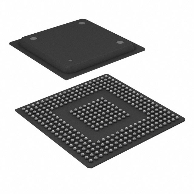
Package : 320-pin plastic BGA (BYA320)
■
CMOS 0.18 m technology
■
Power supply range 3 V to 5 V (1.8 V internal logic provided by
a step-down voltage converter)
■
Operating temperature range: between − 40°C and
+ 105°C/+125°Ca
a. For maximum ambient temperature TA(max), See “Ordering Information” on page 145.
Document Number: 002-04617 Rev. *C
Page 2 of 152
�CY91460Q Series
Contents
Product Lineup .................................................................. 4
Registers .................................................................... 39
Pin Assignment ................................................................. 6
CY91F469QA ............................................................... 6
Embedded Program/Data Memory (Flash) .................... 42
Flash Features ........................................................... 42
Operation Modes........................................................ 42
Flash Access in CPU Mode........................................ 43
Parallel Flash Programming Mode ............................. 45
Poweron Sequence in Parallel Programming Mode... 48
Flash Security............................................................. 48
Notes About Flash Memory CRC Calculation ............ 51
Pin Description .................................................................. 7
CY91F469QA .............................................................. 7
I/O Circuit Types .............................................................. 23
Special Port / Resource Assignments........................... 30
Overview of Special Port / Resource Assignments .... 30
The Second A/D Converter (ADC1) ........................... 30
The Additional External Interrupts (INT16-31)............ 31
Re-located External Interrupts (INT4, INT5, INT10,
INT11, INT12, INT14)................................................. 32
Input Capture Units (ICU8,9) and Free Run Timer (FRT8)
................................................................................... 32
External Bus Function After Reset ............................. 32
Handling Devices............................................................. 33
Preventing Latch-up ................................................... 33
Handling of Unused Input Pins................................... 33
Power Supply Pins ..................................................... 33
Crystal Oscillator Circuit ............................................. 33
Notes on Using External Clock................................... 33
Mode Pins (MD_x)...................................................... 34
Notes on Operating in PLL Clock Mode ..................... 34
Pull-up Control............................................................ 34
Notes on PS Register................................................. 34
Notes on Debugger ......................................................... 35
Execution of the RETI Command............................... 35
Break Function ........................................................... 35
Operand Break ........................................................... 35
Block Diagram ................................................................. 36
CY91F469QA ............................................................ 36
CPU and Control Unit...................................................... 37
Features ..................................................................... 37
Internal Architecture ................................................... 37
Programming Model ................................................... 38
Document Number: 002-04617 Rev. *C
Memory Space ................................................................. 51
Memory Maps................................................................... 52
CY91F469QA ............................................................. 52
I/O Map.............................................................................. 53
CY91F469QA ............................................................. 53
Flash memory and external bus area........................ 82
Interrupt Vector Table ..................................................... 84
Recommended Settings.................................................. 89
PLL and Clockgear Settings....................................... 89
Clock Modulator Settings ........................................... 90
Electrical Characteristics................................................ 96
Absolute Maximum Ratings........................................ 96
Recommended Operating Conditions ........................ 99
DC Characteristics ................................................... 100
A/D Converter Characteristics.................................. 103
Alarm Comparator Characteristics ........................... 107
FLASH Memory Program/erase Characteristics ...... 108
AC Characteristics.................................................... 109
Ordering Information..................................................... 145
Package Dimension....................................................... 146
Revision History ............................................................ 147
Major Changes............................................................... 149
Document History.......................................................... 151
Sales, Solutions, and Legal Information ..................... 152
Page 3 of 152
�CY91460Q Series
1. Product Lineup
Feature
CY91F469QA
100MHz at 1.9V *1
88MHz at 1.8V *2
Max. core frequency (CLKB)
Max. resource frequency
(CLKP)
50MHz
Max. external bus freq. (CLKT)
50MHz
Max. CAN frequency (CLKCAN)
50MHz
Technology
0.18m
Flash memory
2112 KByte
Flash Protection
yes
Flash CRC calculation
yes
D-RAM
64 KByte
ID-RAM
32 KByte
Flash-cache (F-cache)
16 KBytes
External bus cache (I-cache)
4 KBytes
Boot-ROM / BI-ROM
4 KByte
MPU (8 ch) *3
MMU/MPU
DMA
5 ch
Software-Watchdog
yes
Hardware-Watchdog
(RC osc. based)
yes
Bit Search
yes
RTC
1 ch
Free Running Timer
9 ch
ICU
10 ch
OCU
8 ch
Reload Timer
8 ch
PPG 16-bit
16 ch
PFM 16-bit
1 ch
Sound Generator
1 ch
Up/Down Counter (8/16-bit)
4 ch (8-bit) / 2 ch (16-bit)
C_CAN
LIN-USART
3 ch (32msg)
4 ch + 4 ch FIFO + 4 ch FIFO (asynchronous)
I2C (400k)
FR external bus
3 ch
yes (28bit addr, 32bit data, 8 chip selects)
Document Number: 002-04617 Rev. *C
Page 4 of 152
�CY91460Q Series
Feature
External Interrupts
CY91F469QA
32 ch
NMI Interrupts
General IO ports
ADC (10 bit)
205
32 ch + 8 ch
Alarm Comparator
2 ch
Reset input (INITX)
yes
Hardware Standby Input (HSTX)
no
Clock Modulator
yes
Low power mode
yes
Supply Supervisor
yes
Clock Supervisor
yes
Main clock oscillator
4MHz
Sub clock oscillator
32kHz
RC Oscillator
PLL
100kHz / 2MHz
x 25
DSU4
no
EDSU
yes (16 BP) *3
JTAG Boundary Scan
Supply Voltage
Regulator
Power Consumption
Temperature Range (TA)
Package
yes
3V / 5V
yes
MB91F469QAPB-GSK6E1 价格&库存
很抱歉,暂时无法提供与“MB91F469QAPB-GSK6E1”相匹配的价格&库存,您可以联系我们找货
免费人工找货