MB95F394H/F396K/F398H/F394K/F396H/F398K
2
CMOS F MC-8FX MB95390H Series
8-bit Microcontrollers
MB95390H is a series of general-purpose, single-chip microcontrollers. In addition to a compact instruction set, the microcontrollers
of this series contain a variety of peripheral resources.
Features
F2MC-8FX CPU core
UART/SIO 1 channel
Instruction set optimized for controllers
■
Multiplication and division instructions
■
16-bit arithmetic operations
■
Bit test branch instructions
■
Bit manipulation instructions, etc.
■
Capable of clock-asynchronous (UART) serial data transfer
and clock-synchronous (SIO) serial data transfer
■
Built-in wake-up function
Multi-pulse generator (MPG) (for DC motor
control) 1 channel
Selectable main clock source
Main OSC clock (up to 16.25 MHz, maximum machine clock
frequency: 8.125 MHz)
External clock (up to 32.5 MHz, maximum machine clock
frequency: 16.25 MHz)
Main CR clock (1/8/10/12.5 MHz 2% or 2.5%*, maximum
machine clock frequency: 12.5 MHz)
:The main CR clock oscillation accuracy of a product in LQFP
package (FPT-48P-M49 or FPT-52P-M02) is 2% and that of
a product in QFN package (LCC-48P-M11) is 2.5%.
■
Full duplex double buffer
I2C 1 channel
Clock
■
■
Selectable subclock source
■
16-bit reload timer 1 channel
■
16-bit PPG timer 1 channel
■
Waveform sequencer (including a 16-bit timer equipped with a
buffer and a compare clear function)
LIN-UART
■
Full duplex double buffer
■
Capable of clock-synchronous serial data transfer and
clock-asynchronous serial data transfer
External interrupt 8 channels
Sub-OSC clock (32.768 kHz)
External clock (32.768 kHz)
■
Interrupt by edge detection (rising edge, falling edge, and both
edges can be selected)
■
Can be used to wake up the device from different low power
consumption (standby) modes
Sub-CR clock (Typ: 100 kHz, Min: 50 kHz, Max: 200 kHz)
Timer
■
8/16-bit composite timer 2 channels
8/10-bit A/D converter 12 channels
■
8/16-bit PPG 3 channels
■
■
16-bit PPG 1 channel (can work independently or together
with the multi-pulse generator)
■
16-bit reload timer 1 channel (can work independently or
together with the multi-pulse generator)
■
■
8-bit and 10-bit resolution can be chosen.
Low power consumption (standby) modes
■
Stop mode
■
Sleep mode
Time-base timer 1 channel
■
Watch mode
Watch prescaler 1 channel
■
Time-base timer mode
I/O port
■
MB95F394H/F396H/F398H (maximum no. of I/O ports: 44)
General-purpose I/O ports (N-ch open drain) .................... : 3
General-purpose I/O ports (CMOS I/O) ........................... : 41
■
MB95F394K/F396K/F398K (maximum no. of I/O ports: 45)
General-purpose I/O ports (N-ch open drain) .................... : 4
General-purpose I/O ports (CMOS I/O) ........................... : 41
Cypress Semiconductor Corporation
Document Number: 002-07573 Rev. *A
•
198 Champion Court
•
San Jose, CA 95134-1709
•
408-943-2600
Revised March 31, 2016
�MB95390H Series
On-chip debug
Clock supervisor counter
■
1-wire serial control
■
■
Serial writing supported (asynchronous mode)
Programmable port input voltage level
Hardware/software watchdog timer
■
Built-in clock supervisor counter function
CMOS input level / hysteresis input level
■
Built-in hardware watchdog timer
Dual operation Flash memory
■
Built-in software watchdog timer
■
Low-voltage detection reset circuit
■
Built-in low-voltage detector
Flash memory security function
■
Document Number: 002-07573 Rev. *A
The erase/write operation and the read operation can be
executed in different banks (upper bank/lower bank) simultaneously.
Protects the content of the Flash memory
Page 2 of 72
�MB95390H Series
Contents
Product Line-up ................................................................ 3
Packages and Corresponding Products ........................ 5
Differences Among Products and Notes on
Product Selection ............................................................. 6
Pin Assignment ................................................................ 7
Pin Functions .................................................................. 10
I/O Circuit Type ............................................................... 14
Notes On Device Handling ............................................. 17
Pin Connection ............................................................... 17
Power supply pins .......................................................... 17
Block Diagram ................................................................ 19
CPU Core ......................................................................... 20
Interrupt Source Table ................................................... 27
Electrical Characteristics ............................................... 28
Absolute Maximum Ratings .............................................. 28
Recommended Operating Conditions .............................. 30
DC Characteristics ............................................................ 31
AC Characteristics ............................................................ 34
Clock Timing ..................................................................... 34
Document Number: 002-07573 Rev. *A
Source Clock/Machine Clock ............................................ 36
External Reset .................................................................. 38
Power-on Reset ................................................................ 39
Peripheral Input Timing .................................................... 40
LIN-UART Timing ............................................................. 41
Low-voltage Detection ...................................................... 47
I2C Timing ........................................................................ 48
UART/SIO, Serial I/O Timing ............................................ 51
MPG Input Timing ............................................................. 53
A/D Converter ................................................................... 54
A/D Converter Electrical Characteristics .......................... 54
Notes on Using the A/D Converter ................................... 55
Definitions of A/D Converter Terms .................................. 56
Flash Memory Write/Erase Characteristics ...................... 58
Sample Characteristics .................................................. 59
Mask Options .................................................................. 65
Ordering Information ...................................................... 66
Package Dimension ........................................................ 67
Major Changes ............................................................... 70
Page 3 of 72
�MB95390H Series
1. Product Line-up
Part number
MB95F394H
MB95F396H
MB95F398H
MB95F394K
MB95F396K
MB95F398K
Parameter
Type
Clock supervisor
counter
Flash memory product
It supervises the main clock oscillation.
Program ROM
capacity
20 Kbyte
36 Kbyte
60 Kbyte
20 Kbyte
36 Kbyte
60 Kbyte
RAM capacity
496 bytes
1008 bytes
2032 bytes
496 bytes
1008 bytes
2032 bytes
Low-voltage
detection reset
No
Reset input
Yes
Dedicated
CPU functions
General-purpose
I/O
• I/O ports (Max)
• CMOS I/O
• N-ch open drain
Time-base timer
Interval time: 0.256 ms to 8.3 s (with external clock frequency = 4 MHz)
Hardware/software
watchdog timer
• Reset generation cycle
- Main oscillation clock at 10 MHz: 105 ms (Min)
• The sub-CR clock can be used as the source clock of the hardware watchdog timer.
Wild register
It can be used to replace three bytes of data.
LIN-UART
• A wide range of communication speeds can be selected by a dedicated reload timer.
• Clock-synchronous serial data transfer and clock-asynchronous serial data transfer is enabled.
• The LIN function can be used as a LIN master or a LIN slave.
8/10-bit A/D
converter
Number of basic instructions
Instruction bit length
Instruction length
Data bit length
Minimum instruction execution time
Interrupt processing time
Selected through software
•
•
•
•
•
•
: 136
: 8 bits
: 1 to 3 bytes
: 1, 8 and 16 bits
: 61.5 ns (with machine clock frequency = 16.25 MHz)
: 0.6 µs (with machine clock frequency = 16.25 MHz)
: 44
: 41
: 3
• I/O ports (Max)
• CMOS I/O
• N-ch open drain
: 45
: 41
: 4
12 channels
8-bit resolution and 10-bit resolution can be chosen.
2 channels
8/16-bit
composite timer
External
interrupt
On-chip debug
•
•
•
•
The timer can be configured as an "8-bit timer 2 channels" or a "16-bit timer 1 channel".
It has the following functions: timer function, PWC function, PWM function and input capture function.
Count clock: it can be selected from internal clocks (seven types) and external clocks.
It can output square wave.
8 channels
• Interrupt by edge detection (The rising edge, falling edge, or both edges can be selected.)
• It can be used to wake up the device from different standby modes.
• 1-wire serial control
• It supports serial writing. (asynchronous mode)
(Continued)
Document Number: 002-07573 Rev. *A
Page 4 of 72
�MB95390H Series
(Continued)
Part number
MB95F394H
MB95F396H
MB95F398H
MB95F394K
MB95F396K
MB95F398K
Parameter
1 channel
UART/SIO
• Data transfer with UART/SIO is enabled.
• It has a full duplex double buffer, variable data length (5/6/7/8 bits), a built-in baud rate generator and an error
detection function.
• It uses the NRZ type transfer format.
• LSB-first data transfer and MSB-first data transfer are available to use.
• Clock-asynchronous (UART) serial data transfer and clock-synchronous (SIO) serial data transfer is enabled.
1 channel
2
I C
• Master/slave transmission and receiving
• It has the following functions: bus error function, arbitration function, transmission direction detection function,
wake-up function, and functions of generating and detecting repeated START conditions.
3 channels
8/16-bit PPG
• Each channel of PPG can be used as two 8-bit PPG channels or a single 16-bit PPG channel.
• The counter operating clock can be selected from eight clock sources.
16-bit PPG
•
•
•
•
PWM mode and one-shot mode are available to use.
The counter operating clock can be selected from eight clock sources.
It supports external trigger start.
It can work independently or together with the multi-pulse generator.
16-bit reload timer
•
•
•
•
•
Two clock modes and two counter operating modes are available to use.
It can output square waveform.
Count clock: it can be selected from internal clocks (seven types) and external clocks.
Two counter operating modes: reload mode and one-shot mode
It can work independently or together with the multi-pulse generator.
Multi-pulse
generator (for DC
motor control)
•
•
•
•
16-bit PPG timer: 1 channel
16-bit reload timer operations: toggle output, one-shot output
Event counter: 1 channel
Waveform sequencer (including a 16-bit timer equipped with a buffer and a compare clear function)
Watch prescaler
Eight different time intervals can be selected.
Flash memory
• It supports automatic programming, Embedded Algorithm, and write/erase/erase-suspend/erase-resume commands.
• It has a flag indicating the completion of the operation of Embedded Algorithm.
• Number of write/erase cycles: 100000
• Data retention time: 20 years
• Flash security feature for protecting the content of the Flash memory
Standby mode
Sleep mode, stop mode, watch mode, time-base timer mode
Package
Document Number: 002-07573 Rev. *A
FPT-48P-M49
FPT-52P-M02
LCC-48P-M11
Page 5 of 72
�MB95390H Series
2. Packages and Corresponding Products
Part number
MB95F394H
MB95F396H
MB95F398H
MB95F394K
MB95F396K
MB95F398K
O
O
O
O
O
O
Package
FPT-48P-M49
FPT-52P-M02
O
O
O
O
O
O
LCC-48P-M11
O
O
O
O
O
O
O: Available
Document Number: 002-07573 Rev. *A
Page 6 of 72
�MB95390H Series
3. Differences Among Products and Notes on Product Selection
■
Current consumption
When using the on-chip debug function, take account of the current consumption of flash erase/write.
For details of current consumption, see “Electrical Characteristics”.
■
Package
For details of information on each package, see “Packages and Corresponding Products” and “Package Dimension”.
■
Operating voltage
The operating voltage varies, depending on whether the on-chip debug function is used or not.
For details of the operating voltage, see “Electrical Characteristics”.
■
On-chip debug function
The on-chip debug function requires that VCC, VSS and one serial wire be connected to an evaluation tool. For details of the connection
method, refer to “CHAPTER 29 EXAMPLE OF SERIAL PROGRAMMING CONNECTION” in the hardware manual of the MB95390H
Series.
Document Number: 002-07573 Rev. *A
Page 7 of 72
�MB95390H Series
PG2/X1A/SNI2
PG1/X0A/SNI1
1
2
Vcc
C
3
4
P40/AN08
P41/AN09
5
6
P42/AN10
P43/AN11
Vss
PF1/X1
PF0/X0
PF2/RST
P07/INT07/AN07
P06/INT06/AN06
P05/INT05/AN05
P04/INT04/AN04
P03/INT03/AN03
P02/INT02/AN02
P01/INT01/AN01
P00/INT00/AN00
48
47
46
45
44
43
42
41
40
39
38
37
4. Pin Assignment
(TOP VIEW)
LQFP48
36
35
34
33
P67*/OPT5/PPG21/TRG1
P66*/OPT4/PPG20/PPG1
P65*/OPT3/PPG11
P64*/OPT2/PPG10/EC1
32
31
30
29
P63*/OPT1/PPG01/TO11
P62*/OPT0/PPG00/TO10
P61/TI1
P60/DTTI
P44/TO1
7
8
9
28
P77/UI0
P45/SCK
P46/SOT
10
11
27
26
P76/UO0
P75/UCK0
P47/SIN
12
25
P74/EC0
20
21
22
23
24
P17/SNI0
P71/TO01
P72/SCL
P73/SDA
17
18
19
P14/PPG01
P15/PPG20
P16/PPG21
P70/TO00
13
14
15
16
P10/PPG10
P11/PPG11
P12/DBG
P13/PPG00
FPT-48P-M49
*: High-current pin (8 mA/12 mA)
(Continued)
Document Number: 002-07573 Rev. *A
Page 8 of 72
�P02/INT02/AN02
P01/INT01/AN01
42
41
40
7
8
9
FPT-52P-M02
P44/TO1
10
P45/SCK
11
P46/SOT
12
13
39
38
37
36
P67*/OPT5/PPG21/TRG1
P66*/OPT4/PPG20/PPG1
P65*/OPT3/PPG11
P64*/OPT2/PPG10/EC1
35
34
33
32
31
P63*/OPT1/PPG01/TO11
P62*/OPT0/PPG00/TO10
NC
P61/TI1
P60/DTTI
30
P77/UI0
29
P76/UO0
28
27
P75/UCK0
P74/EC0
P73/SDA
P72/SCL
20
17
18
19
P10/PPG10
P11/PPG11
P12/DBG
P13/PPG00
14
15
16
P47/SIN
24
25
26
P42/AN10
P43/AN11
P71/TO01
(TOP VIEW)
LQFP52
23
5
6
22
P40/AN08
P41/AN09
NC
P17/SNI0
3
4
P70/TO00
Vcc
C
21
1
2
P14/PPG01
P15/PPG20
NC
P16/PPG21
PG2/X1A/SNI2
PG1/X0A/SNI1
P00/INT00/AN00
P03/INT03/AN03
43
44
Vss
PF1/X1
PF0/X0
PF2/RST
P07/INT07/AN07
P06/INT06/AN06
NC
P05/INT05/AN05
P04/INT04/AN04
52
51
50
49
48
47
46
45
MB95390H Series
*: High-current pin (8 mA/12 mA)
(Continued)
Document Number: 002-07573 Rev. *A
Page 9 of 72
�MB95390H Series
PG2/X1A/SNI2
PG1/X0A/SNI1
1
2
Vcc
C
3
4
P40/AN08
P41/AN09
5
6
P42/AN10
P43/AN11
P44/TO1
7
8
9
P45/SCK
10
P46/SOT
P47/SIN
Vss
PF1/X1
PF0/X0
PF2/RST
P07/INT07/AN07
P06/INT06/AN06
P05/INT05/AN05
P04/INT04/AN04
P03/INT03/AN03
P02/INT02/AN02
P01/INT01/AN01
P00/INT00/AN00
48
47
46
45
44
43
42
41
40
39
38
37
(Continued)
36
35
34
33
P67*/OPT5/PPG21/TRG1
P66*/OPT4/PPG20/PPG1
P65*/OPT3/PPG11
32
31
30
29
P64*/OPT2/PPG10/EC1
P63*/OPT1/PPG01/TO11
P62*/OPT0/PPG00/TO10
P61/TI1
P60/DTTI
28
P77/UI0
27
P76/UO0
11
26
P75/UCK0
12
25
P74/EC0
(TOP VIEW)
QFN48
21
22
23
24
P70/TO00
P71/TO01
P72/SCL
P73/SDA
P16/PPG21
P17/SNI0
P15/PPG20
17
18
19
20
P14/PPG01
16
15
14
P10/PPG10
P11/PPG11
P12/DBG
P13/PPG00
13
LCC-48P-M11
*: High-current pin (8 mA/12 mA)
Document Number: 002-07573 Rev. *A
Page 10 of 72
�MB95390H Series
5. Pin Functions
Pin no.
LQFP48*1
QFN48*2
LQFP52*3
Pin
name
I/O
circuit
type*4
PG2
1
2
1
2
1
2
X1A
General-purpose I/O port
C
3
3
4
4
4
5
5
5
6
6
6
—
—
7
7
7
8
8
8
9
9
9
10
10
10
11
11
11
12
12
12
13
13
13
14
14
14
15
15
15
16
16
16
17
Subclock I/O oscillation pin
SNI2
Trigger input pin for the position detection function of the MPG
waveform sequencer
PG1
General-purpose I/O port
X0A
C
Subclock input oscillation pin
Trigger input pin for the position detection function of the MPG
waveform sequencer
SNI1
3
Function
VCC
—
Power supply pin
C
—
Capacitor connection pin
P40
AN08
P41
AN09
NC
P42
AN10
P43
AN11
P44
TO1
P45
SCK
P46
SOT
P47
SIN
P10
PPG10
P11
PPG11
P12
DBG
P13
PPG00
K
K
—
K
K
G
G
G
J
G
G
H
G
General-purpose I/O port
A/D converter analog input pin
General-purpose I/O port
A/D converter analog input pin
It is an internally connected pin. Always leave it unconnected.
General-purpose I/O port
A/D converter analog input pin
General-purpose I/O port
A/D converter analog input pin
General-purpose I/O port
16-bit reload timer ch. 0 output pin
General-purpose I/O port
LIN-UART clock I/O pin
General-purpose I/O port
LIN-UART data output pin
General-purpose I/O port
LIN-UART data input pin
General-purpose I/O port
8/16-bit PPG ch. 1 output pin
General-purpose I/O port
8/16-bit PPG ch. 1 output pin
General-purpose I/O port
DBG input pin
General-purpose I/O port
8/16-bit PPG ch. 0 output pin
(Continued)
Document Number: 002-07573 Rev. *A
Page 11 of 72
�MB95390H Series
Pin no.
LQFP48*1
QFN48*2
LQFP52*3
17
17
18
18
18
19
—
—
20
19
19
21
20
20
22
21
21
23
22
22
24
23
23
25
24
24
26
25
25
27
26
26
28
27
27
29
28
28
30
29
29
31
30
30
32
—
—
33
Pin
name
P14
PPG01
P15
PPG20
NC
P16
PPG21
I/O
circuit
type*4
G
G
—
G
P17
SNI0
P70
TO00
P71
TO01
P72
SCL
P73
SDA
P74
EC0
P75
UCK0
P76
UO0
P77
UI0
P60
DTTI
P61
TI1
NC
31
34
OPT0
PPG00
TO10
General-purpose I/O port
8/16-bit PPG ch. 0 output pin
General-purpose I/O port
8/16-bit PPG ch. 2 output pin
It is an internally connected pin. Always leave it unconnected.
General-purpose I/O port
8/16-bit PPG ch. 2 output pin
General-purpose I/O port
G
G
G
I
I
G
G
G
J
G
G
—
Trigger input pin for the position detection function of the MPG
waveform sequencer
General-purpose I/O port
8/16-bit composite timer ch. 0 output pin
General-purpose I/O port
8/16-bit composite timer ch. 0 output pin
General-purpose I/O port
I2C clock I/O pin
General-purpose I/O port
I2C data I/O pin
General-purpose I/O port
8/16-bit composite timer ch. 0 clock input pin
General-purpose I/O port
UART/SIO ch. 0 clock I/O pin
General-purpose I/O port
UART/SIO ch. 0 data output pin
General-purpose I/O port
UART/SIO ch. 0 data input pin
General-purpose I/O port
MPG waveform sequencer input pin
General-purpose I/O port
16-bit reload timer ch. 0 input pin
It is an internally connected pin. Always leave it unconnected.
General-purpose I/O port
High-current pin
P62
31
Function
D
MPG waveform sequencer output pin
8/16-bit PPG ch. 0 output pin
8/16-bit composite timer ch. 1 output pin
(Continued)
Document Number: 002-07573 Rev. *A
Page 12 of 72
�MB95390H Series
Pin no.
LQFP48*1
QFN48*2
LQFP52*3
Pin
name
I/O
circuit
type*4
General-purpose I/O port
High-current pin
P63
32
32
35
OPT1
D
PPG01
8/16-bit composite timer ch. 1 output pin
General-purpose I/O port
High-current pin
P64
33
36
OPT2
D
PPG10
34
34
37
EC1
8/16-bit composite timer ch. 1 clock input pin
P65
General-purpose I/O port
High-current pin
OPT3
D
38
OPT4
General-purpose I/O port
High-current pin
D
36
39
8/16-bit PPG ch. 2 output pin
PPG1
16-bit PPG ch. 1 output pin
General-purpose I/O port
High-current pin
OPT5
D
37
40
8/16-bit PPG ch. 2 output pin
TRG1
16-bit PPG ch. 1 trigger input pin
INT00
General-purpose I/O port
E
AN00
38
41
INT01
General-purpose I/O port
E
AN01
39
42
INT02
General-purpose I/O port
E
AN02
40
43
INT03
AN03
External interrupt input pin
A/D converter analog input pin
P03
40
External interrupt input pin
A/D converter analog input pin
P02
39
External interrupt input pin
A/D converter analog input pin
P01
38
MPG waveform sequencer output pin
PPG21
P00
37
MPG waveform sequencer output pin
PPG20
P67
36
MPG waveform sequencer output pin
8/16-bit PPG ch. 1 output pin
P66
35
MPG waveform sequencer output pin
8/16-bit PPG ch. 1 output pin
PPG11
35
MPG waveform sequencer output pin
8/16-bit PPG ch. 0 output pin
TO11
33
Function
General-purpose I/O port
E
External interrupt input pin
A/D converter analog input pin
(Continued)
Document Number: 002-07573 Rev. *A
Page 13 of 72
�MB95390H Series
(Continued)
Pin no.
LQFP48*1
QFN48*2
LQFP52*3
Pin
name
I/O
circuit
type*4
P04
41
41
44
INT04
General-purpose I/O port
E
AN04
42
45
INT05
General-purpose I/O port
E
AN05
—
—
46
NC
43
47
INT06
—
E
48
INT07
General-purpose I/O port
E
AN07
45
49
46
46
50
47
47
51
48
48
52
RST
PF0
X0
PF1
X1
VSS
External interrupt input pin
A/D converter analog input pin
PF2
45
External interrupt input pin
A/D converter analog input pin
P07
44
It is an internally connected pin. Always leave it unconnected.
General-purpose I/O port
AN06
44
External interrupt input pin
A/D converter analog input pin
P06
43
External interrupt input pin
A/D converter analog input pin
P05
42
Function
General-purpose I/O port
A
B
B
—
Reset pin
Dedicated reset pin in MB95F394H/F396H/F398H
General-purpose I/O port
Main clock I/O oscillation pin
General-purpose I/O port
Main clock I/O oscillation pin
Power supply pin (GND)
*1: Package code: FPT-48P-M49
*2: Package code: LCC-48P-M11
*3: Package code: FPT-52P-M02
*4: For the I/O circuit types, see “I/O Circuit Type”.
Document Number: 002-07573 Rev. *A
Page 14 of 72
�MB95390H Series
6. I/O Circuit Type
Type
Circuit
Remarks
■
N-ch open drain output
■
Hysteresis input
■
Reset output
■
Oscillation circuit
■
High-speed side
■
Feedback resistance:
approx. 1 M
Standby control
■
CMOS output
Hysteresis input
■
Hysteresis input
■
Oscillation circuit
■
Low-speed side
■
Feedback resistance: approx.10 M
■
CMOS output
■
Hysteresis input
■
Pull-up control available
A
Reset input / Hysteresis input
Reset output / Digital output
N-ch
B
P-ch
Port select
Digital output
N-ch
Digital output
Clock input
X1
X0
Standby control / Port select
P-ch
Port select
Digital output
N-ch
Digital output
Standby control
Hysteresis input
C
Port select
R
Pull-up control
P-ch
Digital output
P-ch
N-ch
Digital output
Standby control
Hysteresis input
Clock input
X1A
X0A
Standby control / Port select
Port select
R
Pull-up control
Digital output
Digital output
P-ch
N-ch
Digital output
Standby control
Hysteresis input
Document Number: 002-07573 Rev. *A
Page 15 of 72
�MB95390H Series
Type
Circuit
Remarks
■
CMOS output
Digital output
■
Hysteresis input
Digital output
■
High-current output
■
CMOS output
■
Hysteresis input
■
Pull-up control available
■
Analog input
■
CMOS output
■
Hysteresis input
■
CMOS input
■
Pull-up control available
■
Analog input
■
CMOS output
■
Hysteresis input
■
Pull-up control available
■
N-ch open drain output
■
Hysteresis input
D
P-ch
N-ch
Standby control
Hysteresis input
E
Pull-up control
R
P-ch
Digital output
P-ch
Digital output
N-ch
Analog input
A/D control
Standby control
Hysteresis input
F
Pull-up control
R
P-ch
Digital output
P-ch
Digital output
N-ch
Analog input
A/D control
Standby control
Hysteresis input
CMOS input
G
Pull-up control
R
P-ch
Digital output
P-ch
Digital output
N-ch
Standby control
Hysteresis input
H
Standby control
Hysteresis input
Digital output
N-ch
(Continued)
Document Number: 002-07573 Rev. *A
Page 16 of 72
�MB95390H Series
(Continued)
Type
Circuit
Remarks
I
Digital output
N-ch
Standby control
■
N-ch open drain output
■
Hysteresis input
■
CMOS input
■
CMOS output
■
Hysteresis input
■
CMOS input
■
Pull-up control available
■
Hysteresis input
■
CMOS output
■
Pull-up control available
■
Analog input
Hysteresis input
CMOS input
J
Pull-up control
R
P-ch
Digital output
P-ch
Digital output
N-ch
Standby control
Hysteresis input
CMOS input
K
Pull-up control
R
P-ch
Digital output
P-ch
Digital output
N-ch
Standby control
Hysteresis input
Analog input
Document Number: 002-07573 Rev. *A
Page 17 of 72
�MB95390H Series
7. Notes On Device Handling
■
Preventing latch-ups
When using the device, ensure that the voltage applied does not exceed the maximum voltage rating.
In a CMOS IC, if a voltage higher than VCC or a voltage lower than VSS is applied to an input/output pin that is neither a
medium-withstand voltage pin nor a high-withstand voltage pin, or if a voltage out of the rating range of power supply voltage mentioned
in "14.1 Absolute Maximum Ratings" of “Electrical Characteristics” is applied to the VCC pin or the VSS pin, a latch-up may occur.
When a latch-up occurs, power supply current increases significantly, which may cause a component to be thermally destroyed.
■
Stabilizing supply voltage
Supply voltage must be stabilized.
A malfunction may occur when power supply voltage fluctuates rapidly even though the fluctuation is within the guaranteed operating
range of the VCC power supply voltage.
As a rule of voltage stabilization, suppress voltage fluctuation so that the fluctuation in VCC ripple (p-p value) at the commercial
frequency (50 Hz/60 Hz) does not exceed 10% of the standard VCC value, and the transient fluctuation rate does not exceed 0.1 V/ms
at a momentary fluctuation such as switching the power supply.
■
Notes on using the external clock
When an external clock is used, oscillation stabilization wait time is required for power-on reset, wake-up from subclock mode or stop
mode.
8. Pin Connection
■
Treatment of unused pins
If an unused input pin is left unconnected, a component may be permanently damaged due to malfunctions or latch-ups. Always pull
up or pull down an unused input pin through a resistor of at least 2 k. Set an unused input/output pin to the output state and leave
it unconnected, or set it to the input state and treat it the same as an unused input pin. If there is an unused output pin, leave it
unconnected.
9. Power supply pins
To reduce unnecessary electro-magnetic emission, prevent malfunctions of strobe signals due to an increase in the ground level, and
conform to the total output current standard, always connect the VCC pin and the VSS pin to the power supply and ground outside the
device. In addition, connect the current supply source to the VCC pin and the VSS pin with low impedance.
It is also advisable to connect a ceramic capacitor of approximately 0.1 µF as a bypass capacitor between the VCC pin and the VSS
pin at a location close to this device.
■
DBG pin
Connect the DBG pin directly to an external pull-up resistor.
To prevent the device from unintentionally entering the debug mode due to noise, minimize the distance between the DBG pin and
the VCC or VSS pin when designing the layout of the printed circuit board.
The DBG pin should not stay at “L” level after power-on until the reset output is released.
■
RST pin
Connect the RST pin directly to an external pull-up resistor.
To prevent the device from unintentionally entering the reset mode due to noise, minimize the distance between the RST pin and the
VCC or VSS pin when designing the layout of the printed circuit board.
The RST/PF2 pin functions as the reset input/output pin after power-on. In addition, the reset output of the RST/PF2 pin can be enabled
by the RSTOE bit in the SYSC register, and the reset input function and the general purpose I/O function can be selected by the
RSTEN bit in the SYSC register.
Document Number: 002-07573 Rev. *A
Page 18 of 72
�MB95390H Series
■
C pin
Use a ceramic capacitor or a capacitor with equivalent frequency characteristics. The bypass capacitor for the VCC pin must have a
capacitance larger than CS. For the connection to a smoothing capacitor CS, see the diagram below. To prevent the device from
unintentionally entering a mode to which the device is not set to transit due to noise, minimize the distance between the C pin and CS
and the distance between CS and the VSS pin when designing the layout of a printed circuit board.
• DBG/RST/C pins connection diagram
DBG
C
RST
Cs
Document Number: 002-07573 Rev. *A
Page 19 of 72
�MB95390H Series
10. Block Diagram
F2MC-8FX CPU
PF2*1/RST*2
Dual operation Flash with
security function
(60 Kbyte)
Reset with LVD
PF1/X1*2
PF0/X0*2
Oscillator
circuit
PG2/X1A*2
CR
oscillator
PG1/X0A*2
RAM (496/1008/2032 bytes)
(P04)
Clock control
(P05)
P70/TO00
8/16-bit composite timer ch. 0
P12/DBG*1
On-chip debug
P74/EC0
Wild register
8/10-bit A/D converter
P00/INT00 to P07/INT07
P71/TO01
(P00/AN00 to P07/AN07)
P40/AN08 to P43/AN11
External interrupt
(P62/TO10)
C
Interrupt controller
P45/SCK
P46/SOT
LIN-UART
Internal bus
8/16-bit composite timer ch. 1
(P63/TO11)
(P64/EC1)
MPG
16-bit reload timer
P47/SIN
(P61/TI1)
P44/TO1
P62/OPT0 to P67/OPT5*3
Waveform sequencer
P75/UCK0
P76/UO0
UART/SIO
P17/SNI0, PG1/SNI1, PG2/SNI2
P60/DTTI
P61/TI1
P77/UI0
16-bit PPG timer
P72/SCL*1
I2C
P73/SDA*1
8/16-bit PPG ch. 1
(P62/PPG00*3), P13/PPG00
8/16-bit PPG ch. 0
(P63/PPG01*3), P14/PPG01
(P66/PPG20*3), P15/PPG20
(P67/TRG1)
(P66/PPG1)
P10/PPG10, (P64/PPG10*3)
P11/PPG11, (P65/PPG11*3)
8/16-bit PPG ch. 2
(P67/PPG21*3), P16/PPG21
Port
Vcc
*1: PF2, P12, P72 and P73 are N-ch open drain pins.
Vss
*2: Software option
Port
*3: P62 to P67 are high-current pins.
Note: Pins in parentheses indicate that functions of those pins are shared among different resources.
Document Number: 002-07573 Rev. *A
Page 20 of 72
�MB95390H Series
11. CPU Core
■
Memory Space
The memory space of the MB95390H Series is 64 Kbyte in size, and consists of an I/O area, a data area, and a program area. The
memory space includes areas intended for specific purposes such as general-purpose registers and a vector table. The memory maps
of the MB95390H Series are shown below.
■
Memory Maps
MB95F394H/F394K
MB95F396H/F396K
0000H
0000H
I/O
I/O
0080H
0090H
0100H
Access prohibited
RAM 496 bytes
0080H
0090H
0100H
0200H
Access prohibited
0F80H
Access prohibited
RAM 2032 bytes
Registers
0200H
Access prohibited
0F80H
Flash 4 Kbyte
I/O
0080H
0090H
0100H
0480H
0880H
0F80H
Extended I/O
Extended I/O
1000H
2000H
Access prohibited
RAM 1008 bytes
Registers
Registers
0200H
0280H
MB95F398H/F398K
0000H
1000H
2000H
Flash 4 Kbyte
Access prohibited
Extended I/O
1000H
Vacant
Vacant
7FFFH
Flash 60 Kbyte
Flash 32 Kbyte
BFFFH
Flash 16 Kbyte
FFFFH
Document Number: 002-07573 Rev. *A
FFFFH
FFFFH
Page 21 of 72
�MB95390H Series
12. I/O Map
Address
Register
abbreviation
0000H
PDR0
0001H
0002H
0003H
R/W
Initial value
Port 0 data register
R/W
00000000B
DDR0
Port 0 direction register
R/W
00000000B
PDR1
Port 1 data register
R/W
00000000B
DDR1
Port 1 direction register
R/W
00000000B
0004H
—
0005H
WATR
0006H
—
Register name
(Disabled)
Oscillation stabilization wait time setting register
(Disabled)
—
—
R/W
11111111B
—
—
0007H
SYCC
System clock control register
R/W
0000X011B
0008H
STBC
Standby control register
R/W
00000XXXB
0009H
RSRR
Reset source register
R/W
XXXXXXXXB
000AH
TBTC
Time-base timer control register
R/W
00000000B
000BH
WPCR
Watch prescaler control register
R/W
00000000B
000CH
WDTC
Watchdog timer control register
R/W
00XX0000B
000DH
SYCC2
System clock control register 2
R/W
XX100011B
000EH
to
0011H
—
—
—
(Disabled)
0012H
PDR4
Port 4 data register
R/W
00000000B
0013H
PDR4
Port 4 direction register
R/W
00000000B
0014H,
0015H
—
—
—
0016H
PDR6
Port 6 data register
R/W
00000000B
0017H
DDR6
Port 6 direction register
R/W
00000000B
0018H
DDR7
Port 7 data register
R/W
00000000B
Port 7 direction register
R/W
00000000B
—
—
R/W
00000000B
(Disabled)
0019H
DDR7
001AH
to
0027H
—
0028H
PDRF
Port F data register
(Disabled)
0029H
DDRF
Port F direction register
R/W
00000000B
002AH
PDRG
Port G data register
R/W
00000000B
002BH
DDRG
Port G direction register
R/W
00000000B
002CH
PUL0
Port 0 pull-up register
R/W
00000000B
002DH
PUL1
Port 1 pull-up register
R/W
00000000B
002EH,
002FH
—
—
—
0030H
PUL4
Port 4 pull-up register
R/W
00000000B
0031H
PUL6
Port 6 pull-up register
R/W
00000000B
0032H
PUL7
Port 7 pull-up register
R/W
00000000B
0033H,
0034H
—
—
—
0035H
PULG
R/W
00000000B
(Disabled)
(Disabled)
Port G pull-up register
(Continued)
Document Number: 002-07573 Rev. *A
Page 22 of 72
�MB95390H Series
Address
Register
abbreviation
0036H
T01CR1
0037H
Register name
R/W
Initial value
8/16-bit composite timer 01 status control register 1
R/W
00000000B
T00CR1
8/16-bit composite timer 00 status control register 1
R/W
00000000B
0038H
T11CR1
8/16-bit composite timer 11 status control register 1
R/W
00000000B
0039H
T10CR1
8/16-bit composite timer 10 status control register 1
R/W
00000000B
003AH
PC01
8/16-bit PPG timer 01 control register
R/W
00000000B
003BH
PC00
8/16-bit PPG timer 00 control register
R/W
00000000B
003CH
PC11
8/16-bit PPG timer 11 control register
R/W
00000000B
003DH
PC10
8/16-bit PPG timer 10 control register
R/W
00000000B
003EH
PC21
8/16-bit PPG timer 21 control register
R/W
00000000B
003FH
PC20
8/16-bit PPG timer 20 control register
R/W
00000000B
0040H
TMCSRH1
16-bit reload timer control status register upper
R/W
00000000B
0041H
TMCSRL1
16-bit reload timer control status register lower
R/W
00000000B
0042H,
0043H
—
—
—
0044H
PCNTH1
16-bit PPG status control register upper
R/W
00000000B
0045H
PCNTL1
16-bit PPG status control register lower
R/W
00000000B
0046H,
0047H
—
—
—
0048H
EIC00
External interrupt circuit control register ch. 0/ch. 1
R/W
00000000B
0049H
EIC10
External interrupt circuit control register ch. 2/ch. 3
R/W
00000000B
004AH
EIC20
External interrupt circuit control register ch. 4/ch. 5
R/W
00000000B
004BH
EIC30
External interrupt circuit control register ch. 6/ch. 7
R/W
00000000B
004CH
to
004FH
—
—
—
0050H
SCR
LIN-UART serial control register
R/W
00000000B
0051H
SMR
LIN-UART serial mode register
R/W
00000000B
0052H
SSR
LIN-UART serial status register
R/W
00001000B
0053H
RDR/TDR
LIN-UART receive/transmit data register
R/W
00000000B
0054H
ESCR
LIN-UART extended status control register
R/W
00000100B
(Disabled)
(Disabled)
(Disabled)
0055H
ECCR
LIN-UART extended communication control register
R/W
000000XXB
0056H
SMC10
UART/SIO serial mode control register 1
R/W
00000000B
0057H
SMC20
UART/SIO serial mode control register 2
R/W
00100000B
0058H
SSR0
UART/SIO serial status and data register
R/W
00000001B
R/W
00000000B
R
00000000B
—
—
0059H
TDR0
UART/SIO serial output data register
005AH
RDR0
UART/SIO serial input data register
005BH
to
005FH
—
(Disabled)
(Continued)
Document Number: 002-07573 Rev. *A
Page 23 of 72
�MB95390H Series
Address
Register
abbreviation
0060H
IBCR00
0061H
IBCR10
Register name
I2C bus control register 0
R/W
Initial value
R/W
00000000B
2
R/W
00000000B
2
I C bus control register 1
0062H
IBCR0
I C bus status register
R/W
00000000B
0063H
IDDR0
I2C data register
R/W
00000000B
2
R/W
00000000B
2
R/W
00000000B
0064H
IAAR0
I C address register
0065H
ICCR0
I C clock control register
0066H
OPCUR
Output control register (upper)
R/W
00000000B
0067H
OPCLR
Output control register (lower)
R/W
00000000B
0068H
IPCUR
Input control register (upper)
R/W
00000000B
0069H
IPCLR
Input control register (lower)
R/W
00000000B
006AH
NCCR
Noise cancellation control register
R/W
00000000B
006BH
TCSR
Timer control status register
R/W
00000000B
006CH
ADC1
8/10-bit A/D converter control register 1
R/W
00000000B
006DH
ADC2
8/10-bit A/D converter control register 2
R/W
00000000B
006EH
ADDH
8/10-bit A/D converter data register (upper)
R/W
00000000B
006FH
ADDL
8/10-bit A/D converter data register (lower)
R/W
00000000B
0070H
—
—
—
0071H
FSR2
Flash memory status register 2
R/W
00000000B
0072H
FSR
Flash memory status register
R/W
000X0000B
0073H
SWRE0
Flash memory sector write control register 0
R/W
00000000B
0074H
FSR3
R
00000000B
0075H
—
—
—
(Disabled)
Flash memory status register 3
(Disabled)
0076H
WREN
Wild register address compare enable register
R/W
00000000B
0077H
WROR
Wild register data test setting register
R/W
00000000B
0078H
—
—
—
0079H
ILR0
Interrupt level setting register 0
R/W
11111111B
007AH
ILR1
Interrupt level setting register 1
R/W
11111111B
007BH
ILR2
Interrupt level setting register 2
R/W
11111111B
007CH
ILR3
Interrupt level setting register 3
R/W
11111111B
007DH
ILR4
Interrupt level setting register 4
R/W
11111111B
007EH
ILR5
Interrupt level setting register 5
R/W
11111111B
007FH
—
—
—
Mirror of register bank pointer (RP) and
mirror of direct bank pointer (DP)
(Disabled)
0F80H
WRARH0
Wild register address setting register (upper) ch. 0
R/W
00000000B
0F81H
WRARL0
Wild register address setting register (lower) ch. 0
R/W
00000000B
0F82H
WRDR0
Wild register data setting register ch. 0
R/W
00000000B
(Continued)
Document Number: 002-07573 Rev. *A
Page 24 of 72
�MB95390H Series
Address
Register
abbreviation
0F83H
WRARH1
0F84H
WRARL1
Register name
R/W
Initial value
Wild register address setting register (upper) ch. 1
R/W
00000000B
Wild register address setting register (lower) ch. 1
R/W
00000000B
0F85H
WRDR1
Wild register data setting register ch. 1
R/W
00000000B
0F86H
WRARH2
Wild register address setting register (upper) ch. 2
R/W
00000000B
0F87H
WRARL2
Wild register address setting register (lower) ch. 2
R/W
00000000B
0F88H
WRDR2
Wild register data setting register ch. 2
R/W
00000000B
0F89H
to
0F91H
—
—
—
0F92H
T01CR0
R/W
00000000B
0F93H
T00CR0
8/16-bit composite timer 00 status control register 0
R/W
00000000B
0F94H
T01DR
8/16-bit composite timer 01 data register
R/W
00000000B
(Disabled)
8/16-bit composite timer 01 status control register 0
0F95H
T00DR
8/16-bit composite timer 00 data register
R/W
00000000B
0F96H
TMCR0
8/16-bit composite timer 00/01 timer mode control register
R/W
00000000B
0F97H
T11CR0
8/16-bit composite timer 11 status control register 0
R/W
00000000B
0F98H
T10CR0
8/16-bit composite timer 10 status control register 0
R/W
00000000B
0F99H
T11DR
8/16-bit composite timer 11 data register
R/W
00000000B
0F9AH
T10DR
8/16-bit composite timer 10 data register
R/W
00000000B
0F9BH
TMCR1
8/16-bit composite timer 10/11 timer mode control register
R/W
00000000B
0F9CH
PPS01
8/16-bit PPG01 cycle setting buffer register
R/W
11111111B
0F9DH
PPS00
8/16-bit PPG00 cycle setting buffer register
R/W
11111111B
0F9EH
PDS01
8/16-bit PPG01 duty setting buffer register
R/W
11111111B
0F9FH
PDS00
8/16-bit PPG00 duty setting buffer register
R/W
11111111B
0FA0H
PPS11
8/16-bit PPG11 cycle setting buffer register
R/W
11111111B
0FA1H
PPS10
8/16-bit PPG10 cycle setting buffer register
R/W
11111111B
0FA2H
PDS11
8/16-bit PPG11 duty setting buffer register
R/W
11111111B
0FA3H
PDS10
8/16-bit PPG10 duty setting buffer register
R/W
11111111B
0FA4H
PPGS
8/16-bit PPG startup register
R/W
00000000B
0FA5H
REVC
8/16-bit PPG output reverse register
R/W
00000000B
0FA6H
PPS21
8/16-bit PPG21 cycle setting buffer register
R/W
11111111B
R/W
11111111B
R/W
00000000B
R/W
00000000B
0FA7H
0FA8H
0FA9H
PPS20
8/16-bit PPG20 cycle setting buffer register
TMRH1
16-bit reload timer timer register (upper)
TMRLRH1
16-bit reload timer reload register (upper)
TMRL1
16-bit reload timer timer register (lower)
TMRLRL1
16-bit reload timer reload register (lower)
0FAAH
PDS21
8/16-bit PPG21 duty setting buffer register
R/W
11111111B
0FABH
PDS20
8/16-bit PPG20 duty setting buffer register
R/W
11111111B
(Continued)
Document Number: 002-07573 Rev. *A
Page 25 of 72
�MB95390H Series
Address
Register
abbreviation
Register name
R/W
Initial value
0FACH
to
0FAFH
—
(Disabled)
—
—
0FB0H
PDCRH1
16-bit PPG down counter register (upper)
R
00000000B
0FB1H
PDCRL1
16-bit PPG down counter register (lower)
R
00000000B
0FB2H
PCSRH1
16-bit PPG cycle setting buffer register (upper)
R/W
11111111B
0FB3H
PCSRL1
16-bit PPG cycle setting buffer register (lower)
R/W
11111111B
0FB4H
PDUTH1
16-bit PPG duty setting buffer register (upper)
R/W
11111111B
0FB5H
PDUTL1
16-bit PPG duty setting buffer register (lower)
R/W
11111111B
0FB6H
to
0FBBH
—
—
—
0FBCH
BGR1
LIN-UART baud rate generator register 1
R/W
00000000B
0FBDH
BGR0
LIN-UART baud rate generator register 0
R/W
00000000B
0FBEH
PSSR0
UART/SIO prescaler select register
R/W
00000000B
0FBFH
BRSR0
UART/SIO baud rate setting register
R/W
00000000B
0FC0H,
0FC1H
—
—
—
0FC2H
AIDRH
A/D input disable register (upper)
R/W
00000000B
0FC3H
AIDRL
A/D input disable register (lower)
R/W
00000000B
0FC4H
OPDBRH0
Output data buffer register (upper) ch. 0
R/W
00000000B
0FC5H
OPDBRL0
Output data buffer register (lower) ch. 0
R/W
00000000B
0FC6H
OPDBRH1
Output data buffer register (upper) ch. 1
R/W
00000000B
0FC7H
OPDBRL1
Output data buffer register (lower) ch. 1
R/W
00000000B
0FC8H
OPDBRH2
Output data buffer register (upper) ch. 2
R/W
00000000B
0FC9H
OPDBRL2
Output data buffer register (lower) ch. 2
R/W
00000000B
0FCAH
OPDBRH3
Output data buffer register (upper) ch. 3
R/W
00000000B
0FCBH
OPDBRL3
Output data buffer register (lower) ch. 3
R/W
00000000B
0FCCH
OPDBRH4
Output data buffer register (upper) ch. 4
R/W
00000000B
0FCDH
OPDBRL4
Output data buffer register (lower) ch. 4
R/W
00000000B
0FCEH
OPDBRH5
Output data buffer register (upper) ch. 5
R/W
00000000B
0FCFH
OPDBRL5
Output data buffer register (lower) ch. 5
R/W
00000000B
0FD0H
OPDBRH6
Output data buffer register (upper) ch. 6
R/W
00000000B
0FD1H
OPDBRL6
Output data buffer register (lower) ch. 6
R/W
00000000B
0FD2H
OPDBRH7
Output data buffer register (upper) ch. 7
R/W
00000000B
0FD3H
OPDBRL7
Output data buffer register (lower) ch. 7
R/W
00000000B
0FD4H
OPDBRH8
Output data buffer register (upper) ch. 8
R/W
00000000B
0FD5H
OPDBRL8
Output data buffer register (lower) ch. 8
R/W
00000000B
0FD6H
OPDBRH9
Output data buffer register (upper) ch. 9
R/W
00000000B
0FD7H
OPDBRL9
Output data buffer register (lower) ch. 9
R/W
00000000B
0FD8H
OPDBRHA
Output data buffer register (upper) ch. A
R/W
00000000B
0FD9H
OPDBRLA
Output data buffer register (lower) ch. A
R/W
00000000B
(Disabled)
(Disabled)
(Continued)
Document Number: 002-07573 Rev. *A
Page 26 of 72
�MB95390H Series
(Continued)
Address
Register
abbreviation
0FDAH
OPDBRHB
0FDBH
OPDBRLB
0FDCH
OPDUR
Output data register (upper)
0FDDH
OPDLR
Output data register (lower)
0FDEH
CPCUR
Compare clear register (upper)
Compare clear register (lower)
R/W
XXXXXXXXB
—
—
Register name
R/W
Initial value
Output data buffer register (upper) ch. B
R/W
00000000B
Output data buffer register (lower) ch. B
R/W
00000000B
R
0000XXXXB
R
XXXXXXXXB
R/W
XXXXXXXXB
0FDFH
CPCLR
0FE0H,
0FE1H
—
0FE2H
TMBUR
Timer buffer register (upper)
R
XXXXXXXXB
0FE3H
TMBLR
Timer buffer register (lower)
R
XXXXXXXXB
0FE4H
CRTH
Main CR clock trimming register (upper)
R/W
0XXXXXXXB
0FE5H
CRTL
Main CR clock trimming register (lower)
R/W
00XXXXXXB
0FE6H,
0FE7H
—
—
—
0FE8H
SYSC
System configuration register
R/W
11000011B
R/W
00000000B
(Disabled)
(Disabled)
0FE9H
CMCR
Clock monitoring control register
0FEAH
CMDR
Clock monitoring data register
R
00000000B
0FEBH
WDTH
Watchdog timer selection ID register (upper)
R
XXXXXXXXB
0FECH
WDTL
Watchdog timer selection ID register (lower)
R
XXXXXXXXB
0FEDH
—
0FEEH
ILSR
0FEFH
WICR
0FF0H
to
0FFFH
—
(Disabled)
—
—
Input level select register
R/W
00000000B
Interrupt pin control register
R/W
01000000B
—
—
■
R/W access symbols
R/W
: Readable / Writable
R
: Read only
W
: Write only
■
Initial value symbols
0
: The initial value of this bit is “0”.
1
: The initial value of this bit is “1”.
X
: The initial value of this bit is indeterminate.
(Disabled)
Note: Do not write to an address that is “(Disabled)”. If a “(Disabled)” address is read, an indeterminate value is returned.
Document Number: 002-07573 Rev. *A
Page 27 of 72
�MB95390H Series
13. Interrupt Source Table
Interrupt source
Interrupt
request
number
Vector table address
Upper
Lower
Bit name of
interrupt level
setting register
External interrupt ch. 0, ch. 4
IRQ00
FFFAH
FFFBH
L00 [1:0]
External interrupt ch. 1, ch. 5
IRQ01
FFF8H
FFF9H
L01 [1:0]
External interrupt ch. 2, ch. 6
IRQ02
FFF6H
FFF7H
L02 [1:0]
External interrupt ch. 3, ch. 7
IRQ03
FFF4H
FFF5H
L03 [1:0]
UART/SIO ch. 0, MPG (DTTI)
IRQ04
FFF2H
FFF3H
L04 [1:0]
8/16-bit composite timer ch. 0 (lower)
IRQ05
FFF0H
FFF1H
L05 [1:0]
8/16-bit composite timer ch. 0 (upper)
IRQ06
FFEEH
FFEFH
L06 [1:0]
LIN-UART (reception)
IRQ07
FFECH
FFEDH
L07 [1:0]
LIN-UART (transmission)
IRQ08
FFEAH
FFEBH
L08 [1:0]
8/16-bit PPG ch. 1 (lower)
IRQ09
FFE8H
FFE9H
L09 [1:0]
8/16-bit PPG ch. 1 (upper)
IRQ10
FFE6H
FFE7H
L10 [1:0]
8/16-bit PPG ch. 2 (upper)
IRQ11
FFE4H
FFE5H
L11 [1:0]
8/16-bit PPG ch. 0 (upper)
IRQ12
FFE2H
FFE3H
L12 [1:0]
8/16-bit PPG ch. 0 (lower)
IRQ13
FFE0H
FFE1H
L13 [1:0]
8/16-bit composite timer ch. 1 (upper)
IRQ14
FFDEH
FFDFH
L14 [1:0]
8/16-bit PPG ch. 2 (lower)
IRQ15
FFDCH
FFDDH
L15 [1:0]
16-bit reload timer ch. 1, MPG (write
timing/compare clear),
I2 C
IRQ16
FFDAH
FFDBH
L16 [1:0]
16-bit PPG timer ch. 1, MPG (position
detection/compare match)
IRQ17
FFD8H
FFD9H
L17 [1:0]
8/10-bit A/D converter
IRQ18
FFD6H
FFD7H
L18 [1:0]
Time-base timer
IRQ19
FFD4H
FFD5H
L19 [1:0]
Watch prescaler
IRQ20
FFD2H
FFD3H
L20 [1:0]
IRQ21
FFD0H
FFD1H
L21 [1:0]
8/16-bit composite timer ch. 1 (lower)
IRQ22
FFCEH
FFCFH
L22 [1:0]
Flash memory
IRQ23
FFCCH
FFCDH
L23 [1:0]
—
Priority order of
interrupt sources
of the same level
(occurring
simultaneously)
High
Low
Document Number: 002-07573 Rev. *A
Page 28 of 72
�MB95390H Series
14. Electrical Characteristics
14.1 Absolute Maximum Ratings
Parameter
Power supply voltage*1
Input voltage*
1
Output voltage*
1
Maximum clamp current
Total maximum clamp current
“L” level maximum output
current
Symbol
Rating
Unit
Remarks
Min
Max
VCC
VSS 0.3
VSS 6
V
VI
VSS 0.3
VSS 6
V
*2
VO
VSS 0.3
VSS 6
V
*2
ICLAMP
2
2
mA
Applicable to specific pins*3
|ICLAMP|
—
20
mA
Applicable to specific pins*3
IOL1
—
15
IOL2
—
15
IOLAV1
—
4
mA
mA
“L” level average current
Other than P62 to P67
P62 to P67
Other than P62 to P67
Average output current =
operating current operating ratio
(1 pin)
P62 to P67
Average output current =
operating current operating ratio
(1 pin)
IOLAV2
—
12
“L” level total maximum output
current
IOL
—
100
mA
“L” level total average output
current
IOLAV
—
50
mA
IOH1
—
15
IOH2
—
15
P12, P62 to P67, P72, P73 and PF2
4
Other than P12, P62 to P67, P72, P73 and
PF2
Average output current =
operating current operating ratio
(1 pin)
“H” level maximum output
current
IOHAV1
—
mA
mA
“H” level average current
Other than P12, P62 to P67, P72, P73 and
PF2
P12, P62 to P67, P72, P73 and PF2
Average output current =
operating current operating ratio
(1 pin)
IOHAV2
—
8
“H” level total maximum output
current
IOH
—
100
mA
“H” level total average output
current
IOHAV
—
50
mA
Power consumption
Pd
—
320
mW
Operating temperature
TA
40
85
C
Tstg
55
150
C
Storage temperature
Total average output current =
operating current operating ratio
(Total number of pins)
Total average output current =
operating current operating ratio
(Total number of pins)
(Continued)
Document Number: 002-07573 Rev. *A
Page 29 of 72
�MB95390H Series
(Continued)
*1: The parameter is based on VSS = 0.0 V.
*2: VI and VO must not exceed VCC 0.3 V. VI must not exceed the rated voltage. However, if the maximum current to/from an input
is limited by means of an external component, the ICLAMP rating is used instead of the VI rating.
*3: Applicable to the following pins: P00 to P07, P10, P11, P13 to P17, P40 to P47, P60 to P67, P70, P71, P74 to P77, PF0, PF1,
PG1 and PG2
• Use under recommended operating conditions.
• Use with DC voltage (current).
• The HV (High Voltage) signal is an input signal exceeding the VCC voltage. Always connect a limiting resistor between the HV
(High Voltage) signal and the microcontroller before applying the HV (High Voltage) signal.
• The value of the limiting resistor should be set to a value at which the current to be input to the microcontroller pin when the HV
(High Voltage) signal is input is below the standard value, irrespective of whether the current is transient current or stationary
current.
• When the microcontroller drive current is low, such as in low power consumption modes, the HV (High Voltage) input potential
may pass through the protective diode to increase the potential of the VCC pin, affecting other devices.
• If the HV (High Voltage) signal is input when the microcontroller power supply is off (not fixed at 0 V), since power is supplied
from the pins, incomplete operations may be executed.
• If the HV (High Voltage) input is input after power-on, since power is supplied from the pins, the voltage of power supply may
not be sufficient to enable a power-on reset.
• Do not leave the HV (High Voltage) input pin unconnected.
• Example of a recommended circuit
• Input/Output equivalent circuit
Protective diode
VCC
HV(High Voltage) input (0 V to 16 V)
P-ch
Limiting
resistor
N-ch
R
WARNING:
Semiconductor devices can be permanently damaged by application of stress (voltage, current, temperature, etc.) in
excess of absolute maximum ratings. Do not exceed these ratings.
Document Number: 002-07573 Rev. *A
Page 30 of 72
�MB95390H Series
14.2 Recommended Operating Conditions
(VSS = 0.0 V)
Parameter
Power supply
voltage
Symbol
VCC
Smoothing
capacitor
CS
Operating
temperature
TA
Value
Min
Max
2.4*1*2
5.5*1
2.3
5.5
2.9
5.5
2.3
5.5
0.022
1
40
85
5
35
Unit
Remarks
In normal operation
V
Hold condition in stop mode
In normal operation
Hold condition in stop mode
µF
C
Other than on-chip debug mode
On-chip debug mode
*3
Other than on-chip debug mode
On-chip debug mode
*1: The value varies depending on the operating frequency, the machine clock and the analog guaranteed range.
*2: This value becomes 2.88 V when the low-voltage detection reset is used.
*3: Use a ceramic capacitor or a capacitor with equivalent frequency characteristics. The bypass capacitor for the VCC pin must have
a capacitance larger than CS. For the connection to a smoothing capacitor CS, see the diagram below. To prevent the device from
unintentionally entering an unknown mode due to noise, minimize the distance between the C pin and CS and the distance between
CS and the VSS pin when designing the layout of a printed circuit board.
• DBG / RST / C pins connection diagram
*
DBG
C
RST
Cs
*: Since the DBG pin becomes a communication pin in on-chip debug mode,
set a pull-up resistor value suiting the input/output specifications of P12/DBG.
WARNING:
The recommended operating conditions are required in order to ensure the normal operation of
the semiconductor device. All of the device's electrical characteristics are warranted when the
device is operated within these ranges.
Always use semiconductor devices within their recommended operating condition ranges.
Operation outside these ranges may adversely affect reliability and could result in device failure.
No warranty is made with respect to uses, operating conditions, or combinations not represented
on the data sheet. Users considering application outside the listed conditions are advised to contact
their representatives beforehand.
Document Number: 002-07573 Rev. *A
Page 31 of 72
�MB95390H Series
14.3 DC Characteristics
Parameter
"H" level input
voltage
“L” level input
voltage
Open-drain
output
application
voltage
“H” level output
voltage
“L” level output
voltage
Input leak
current (Hi-Z
output leak
current)
Pull-up
resistance
(VCC = 5.0 V10%, VSS = 0.0 V, TA = 40C to 85C)
Symbol
Pin name
Condition
VIHI
P47, P72, P73, P77
Value
Unit
Remarks
VCC 0.3
V
When CMOS input level
(hysteresis input) is
selected
—
VCC 0.3
V
Hysteresis input
0.7 VCC
—
VCC 0.3
V
Hysteresis input
*1
VSS 0.3
—
0.3 VCC
V
When CMOS input level
(hysteresis input) is
selected
VILS
P00 to P07,
P10 to P17,
P40 to P47,
P60 to P67,
P70 to P77, PF0,
PF1, PG1, PG2
*1
VSS 0.3
—
0.2 VCC
V
Hysteresis input
VILM
PF2
—
VSS 0.3
—
0.3 VCC
V
Hysteresis input
P12, P72, P73, PF2
—
VSS 0.3
—
VSS 5.5
V
Min
Typ*3
Max
*1
0.7 VCC
—
VIHS
P00 to P07,
P10 to P17,
P40 to P47,
P60 to P67,
P70 to P77, PF0,
PF1, PG1, PG2
*1
0.8 VCC
VIHM
PF2
—
VIL
P47, P72, P73, P77
VD
VOH1
Output pins other
than P12, P62 to
IOH = 4 mA
P67, P72, P73, PF2
VCC 0.5
—
—
V
VOH2
P62 to P67
IOH = 8 mA
VCC 0.5
—
—
V
VOL1
Output pins other
than
P62 to P67
IOL = 4 mA
—
—
0.4
V
VOL2
P62 to P67
IOL = 12 mA
—
—
0.4
V
All input pins
0.0 V < VI < VCC
5
—
5
µA
When pull-up resistance
is disabled
P00 to P07, P10,
P11,
P13 to P17,
P40 to P47, P60,
P61,
P70, P71,
P74 to P76, PG1,
PG2
VI = 0 V
25
50
100
k
When pull-up resistance
is enabled
ILI
RPULL
(Continued)
Document Number: 002-07573 Rev. *A
Page 32 of 72
�MB95390H Series
(VCC = 5.0 V10%, VSS = 0.0 V, TA = 40C to 85C)
Parameter
Input
capacitance
Symbol
Pin name
Condition
Value
Unit
Remarks
Min
Typ*3
Max
—
5
15
pF
—
14.8
17
Except during Flash
mA memory writing and
erasing
—
33.5
39.5
—
16.6
21
mA At A/D conversion
VCC = 5.5 V
FCH = 32 MHz
FMP = 16 MHz
Main sleep mode
(divided by 2)
—
7
9
mA
VCC = 5.5 V
FCL = 32 kHz
FMPL = 16 kHz
Subclock mode
(divided by 2)
TA = 25C
—
60
153
µA
ICCLS
VCC = 5.5 V
FCL = 32 kHz
FMPL = 16 kHz
Subsleep mode
(divided by 2)
TA = 25C
—
9.4
84
µA
ICCT
VCC = 5.5 V
FCL = 32 kHz
Watch mode
Main stop mode
TA = 25C
—
4.3
30
µA
VCC = 5.5 V
FCRH = 12.5 MHz
FMP = 12.5 MHz
Main CR clock
mode
—
11.8
13.2
mA
VCC = 5.5 V
Sub-CR clock mode
(divided by 2)
TA = 25C
—
113
410
µA
CIN
Other than VCC and
f = 1 MHz
VSS
VCC = 5.5 V
FCH = 32 MHz
FMP = 16 MHz
Main clock mode
(divided by 2)
ICC
ICCS
ICCL
VCC
(External clock
operation)
Power supply
current*2
ICCMCR
VCC
ICCSCR
mA
During Flash memory
writing and erasing
(Continued)
Document Number: 002-07573 Rev. *A
Page 33 of 72
�MB95390H Series
(Continued)
Parameter
(VCC = 5.0 V10%, VSS = 0.0 V, TA = 40C to 85C)
Symbol
Condition
Value
Unit
Min
Typ*3
Max
VCC = 5.5 V
FCH = 32 MHz
Time-base timer mode
TA = 25C
—
0.9
3
mA
ICCH
VCC = 5.5 V
Substop mode
TA = 25C
—
3.4
22.5
µA
ILVD
Current consumption for
low-voltage detection
circuit only
—
31
54
µA
Current consumption for
the main CR oscillator
—
0.5
0.6
mA
Current consumption for
the sub-CR oscillator
oscillating at 100 kHz
—
20
72
µA
ICCTS
Power supply
current*2
Pin name
ICRH
VCC
(External clock
operation)
VCC
ICRL
Remarks
*1: The input levels of P47, P72, P73 and P77 can be switched between “CMOS input level” and “hysteresis input level”. The input
level selection register (ILSR) is used to switch between the two input levels.
*2: • The power supply current is determined by the external clock. When the low-voltage detection option is selected, the power-supply
current will be the sum of adding the current consumption of the low-voltage detection circuit (ILVD) to one of the value from ICC
to ICCH. In addition, when both the low-voltage detection option and the CR oscillator are selected, the power supply current will
be the sum of adding up the current consumption of the low-voltage detection circuit, the current consumption of the CR oscillators
(ICRH, ICRL) and a specified value. In on-chip debug mode, the CR oscillator (ICRH) and the low-voltage detection circuit are
always enabled, and current consumption therefore increases accordingly.
• See "AC Characteristics: Clock Timing" for FCH and FCL.
• See "AC Characteristics: Source Clock/Machine Clock" for FMP and FMPL.
*3: VCC = 5.0 V, TA = 25C
Document Number: 002-07573 Rev. *A
Page 34 of 72
�MB95390H Series
14.4 AC Characteristics
14.4.1 Clock Timing
Parameter
(VCC = 2.4 V to 5.5 V, VSS = 0.0 V, TA = 40C to 85C)
Symbol
Pin name
When the main oscillation circuit is
used
1
—
16.25
X1: open
1
—
12
*1
1
—
32.5
MHz When the main external clock is
MHz used
12.25
12.5
12.75
MHz
9.80
10
10.20
MHz
7.84
8
8.16
MHz
0.98
1
1.02
MHz
12.18
12.5
12.82
MHz
9.75
10
10.25
MHz
7.80
8
8.20
MHz
0.97
1
1.03
MHz
—
32.768
—
kHz
When the sub-oscillation circuit is
used
—
32.768
—
kHz
When the sub-external clock is
used
—
50
100
200
kHz
When the sub-CR clock is used
—
61.5
—
1000
ns
X1: open
83.4
—
1000
ns
X0, X1
*1
30.8
—
1000
ns
tLCYL
X0A, X1A
—
—
30.5
—
µs
tWH1
tWL1
X0
X0
FCRH
—
X0A, X1A
FCRL
—
X0, X1
CR oscillation start
time
MHz
—
FCL
Input clock rise
time and fall time
Remarks
Max
X0, X1
Input clock pulse
width
Unit
Typ
FCH
Clock cycle time
Value
Min
X0, X1
Clock frequency
Condition
tHCYL
tWH2
tWL2
tCR
tCF
X0
—
—
X1: open
33.4
—
—
ns
X0, X1
*1
12.4
—
—
ns
X0A
—
—
15.2
—
µs
X1: open
—
—
5
ns
*1
—
—
5
ns
X0
X0, X1
When the main CR clock is used*2
When the main CR clock is used*3
When the main oscillation circuit is
used
When the external clock is used
When the subclock is used
When the external clock is used,
the duty ratio should range
between 40% and 60%.
When the external clock is used
tCRHWK
—
—
—
—
80
µs
When the main CR clock is used
tCRLWK
—
—
—
—
10
µs
When the sub-CR clock is used
*1: The external clock signal is input to X0 and the inverted external clock signal to X1.
*2: These specifications are only applicable to a product in LQFP package (FPT-48P-M49 or FPT-52P-M02).
*3: These specifications are only applicable to a product in QFN package (LCC-48P-M11).
Document Number: 002-07573 Rev. *A
Page 35 of 72
�MB95390H Series
• Input waveform generated when an external clock (main clock) is used
tHCYL
tWH1
tWL1
tCR
tCF
0.8 VCC 0.8 VCC
X0, X1
0.2 VCC
0.2 VCC
0.2 VCC
• Figure of main clock input port external connection
When a crystal oscillator or
a ceramic oscillator is used
X0
When the external clock is used When the external clock
(X1 is open)
is used
X0
X1
X1
X0
X1
Open
FCH
FCH
FCH
• Input waveform generated when an external clock (subclock) is used
tLCYL
tWH2
tCR
tWL2
tCF
0.8 VCC 0.8 VCC
X0A
0.2 VCC
0.2 VCC
0.2 VCC
• Figure of subclock input port external connection
When a crystal oscillator or
a ceramic oscillator is used
X0A
X1A
FCL
When the external clock
is used
X0A
X1A
Open
FCL
Document Number: 002-07573 Rev. *A
Page 36 of 72
�MB95390H Series
14.4.2 Source Clock/Machine Clock
Parameter
Source clock
cycle time*1
Symbol
tSCLK
Pin
name
—
FSP
Source clock
frequency
—
FSPL
Machine clock
cycle time*2
(minimum
instruction
execution time)
tMCLK
Value
Unit
—
FMPL
Remarks
Min
Typ
Max
61.5
—
2000
ns
When the main external clock is used
Min: FCH = 32.5 MHz, divided by 2
Max: FCH = 1 MHz, divided by 2
80
—
1000
ns
When the main CR clock is used
Min: FCRH = 12.5 MHz
Max: FCRH = 1 MHz
—
61
—
µs
When the sub-oscillation clock is used
FCL = 32.768 kHz, divided by 2
—
20
—
µs
When the sub-CR clock is used
FCRL = 100 kHz, divided by 2
0.5
—
16.25
MHz
When the main oscillation clock is used
1
—
12.5
MHz
When the main CR clock is used
—
16.384
—
kHz
When the sub-oscillation clock is used
—
50
—
kHz
When the sub-CR clock is used
FCRL = 100 kHz, divided by 2
61.5
—
32000
ns
When the main oscillation clock is used
Min: FSP = 16.25 MHz, no division
Max: FSP = 0.5 MHz, divided by 16
80
—
16000
ns
When the main CR clock is used
Min: FSP = 12.5 MHz
Max: FSP = 1 MHz, divided by 16
61
—
976.5
µs
When the sub-oscillation clock is used
Min: FSPL = 16.384 kHz, no division
Max: FSPL = 16.384 kHz, divided by 16
20
—
320
µs
When the sub-CR clock is used
Min: FSPL = 50 kHz, no division
Max: FSPL = 50 kHz, divided by 16
0.031
—
16.25
MHz
0.0625
—
12.5
MHz
When the main CR clock is used
1.024
—
16.384
kHz
When the sub-oscillation clock is used
3.125
—
50
kHz
When the sub-CR clock is used
FCRL = 100 kHz
—
FMP
Machine clock
frequency
(VCC = 5.0 V10%, VSS = 0.0 V, TA = 40C to 85C)
When the main oscillation clock is used
*1: This is the clock before it is divided according to the division ratio set by the machine clock divide ratio select bits (SYCC:DIV1,
DIV0). This source clock is divided to become a machine clock according to the divide ratio set by the machine clock divide ratio
select bits (SYCC:DIV1, DIV0). In addition, a source clock can be selected from the following.
• Main clock divided by 2
• Main CR clock
• Subclock divided by 2
• Sub-CR clock divided by 2
*2: This is the operating clock of the microcontroller. A machine clock can be selected from the following.
• Source clock (no division)
• Source clock divided by 4
• Source clock divided by 8
• Source clock divided by 16
Document Number: 002-07573 Rev. *A
Page 37 of 72
�MB95390H Series
• Schematic diagram of the clock generation block
Divided
by 2
FCH
(Main oscillation)
FCRH
(Main CR clock)
FCL
(Sub-oscillation)
FCRL
(Sub-CR clock)
SCLK
(Source clock)
Divided
by 2
Divided
by 2
Clock mode select bits
(SYCC2: RCS1, RCS0)
Division
circuit
× 1
× 1/4
× 1/8
×1/16
MCLK
(Machine clock)
Machine clock divide ratio select bits
(SYCC:DIV1, DIV0)
• Operating voltage - Operating frequency (When TA = 40C to 85C)
MB95390H (without the on-chip debug function)
5.5
Operating voltage (V)
5.0
A/D converter operation range
4.0
3.5
3.0
2.4
16 kHz
3 MHz
10 MHz
16.25 MHz
Source clock frequency (FSP/FSPL)
• Operating voltage - Operating frequency (When TA = 40C to 85C)
MB95390H (with the on-chip debug function)
5.5
Operating voltage (V)
5.0
A/D converter operation range
4.0
3.5
2.9
3.0
16 kHz
3 MHz
12.5 MHz
16.25 MHz
Source clock frequency (FSP)
Document Number: 002-07573 Rev. *A
Page 38 of 72
�MB95390H Series
14.4.3 External Reset
Parameter
(VCC = 5.0 V10%, VSS = 0.0 V, TA = 40C to 85C)
Value
Symbol
Min
Max
2 tMCLK*1
RST “L” level
pulse width
tRSTL
Unit
Remarks
—
ns
In normal operation
Oscillation time of the oscillator*
100
—
µs
In stop mode, subclock mode, subsleep
mode, watch mode, and power-on
100
—
µs
In time-base timer mode
2
*1: See “Source Clock/Machine Clock” for tMCLK.
*2: The oscillation time of an oscillator is the time for it to reach 90% of its amplitude. The crystal oscillator has an oscillation time of
between several ms and tens of ms. The ceramic oscillator has an oscillation time of between hundreds of µs and several ms.
The external clock has an oscillation time of 0 ms. The CR oscillator clock has an oscillation time of between several µs and several
ms.
• In normal operation
tRSTL
RST
0.2 VCC
0.2 VCC
• In stop mode, subclock mode, subsleep mode, watch mode and power-on
tRSTL
RST
X0
0.2 VCC
0.2 VCC
90% of
amplitude
Internal
operating
clock
Oscillation
time of
oscillator
Internal reset
Document Number: 002-07573 Rev. *A
100 μs
Oscillation stabilization wait time
Execute instruction
Page 39 of 72
�MB95390H Series
14.4.4 Power-on Reset
Parameter
(VSS = 0.0 V, TA = 40C to 85C)
Symbol
Condition
Power supply rising time
tR
Power supply cutoff time
tOFF
Value
Unit
Min
Max
—
—
50
ms
—
1
—
ms
tR
Remarks
Wait time until power-on
tOFF
2.5 V
VCC
0.2 V
0.2 V
0.2 V
Note: A sudden change of power supply voltage may activate the power-on reset function. When changing the power supply voltage
during the operation, set the slope of rising to a value below within 30 mV/ms as shown below.
VCC
2.3 V
Set the slope of rising to
a value below 30 mV/ms.
Hold condition in stop mode
VSS
Document Number: 002-07573 Rev. *A
Page 40 of 72
�MB95390H Series
14.4.5 Peripheral Input Timing
Parameter
Peripheral input “H” pulse width
Peripheral input “L” pulse width
(VCC = 5.0 V10%, VSS = 0.0 V, TA = 40C to 85C)
Symbol
tILIH
tIHIL
Value
Pin name
Min
INT00 to INT07, EC0, EC1,TI1, TRG1
Max
Unit
2 tMCLK*
—
ns
*
—
ns
2 tMCLK
*: See “Source Clock/Machine Clock” for tMCLK.
tILIH
INT00 to INT07,
EC0, EC1, TI1,
TRG1
Document Number: 002-07573 Rev. *A
0.8 VCC
tIHIL
0.8 VCC
0.2 VCC
0.2 VCC
Page 41 of 72
�MB95390H Series
14.4.6 LIN-UART Timing
Sampling is executed at the rising edge of the sampling clock*1, and serial clock delay is disabled*2.
(ESCR register: SCES bit = 0, ECCR register: SCDE bit = 0)
(VCC = 5.0 V10%, AVSS = VSS = 0.0 V, TA = 40C to 85C)
Parameter
Serial clock cycle time
Symbol
tSCYC
Pin name
SCK
SCK SOT delay time
tSLOVI
SCK, SOT
Valid SIN SCK
tIVSHI
SCK, SIN
SCK valid SIN hold time
tSHIXI
SCK, SIN
Serial clock “L” pulse width
tSLSH
Max
5 tMCLK*3
—
ns
95
95
ns
tMCLK*3 190
—
ns
0
—
ns
—
ns
*3
*3
tSHSL
SCK
tSLOVE
SCK, SOT
Valid SIN SCK
tIVSHE
SCK, SIN
SCK, SIN
tMCLK
External clock
operation output pin:
CL = 80 pF 1 TTL
Unit
Min
3 tMCLK
SCK SOT delay time
tSHIXE
Internal clock
operation output pin:
CL = 80 pF 1 TTL
Value
SCK
Serial clock “H” pulse width
SCK valid SIN hold time
Condition
tR
95
—
ns
—
2 tMCLK*3 95
ns
190
—
ns
3
tMCLK* 95
—
ns
SCK fall time
tF
SCK
—
10
ns
SCK rise time
tR
SCK
—
10
ns
*1: There is a function used to choose whether the sampling of reception data is performed at a rising edge or a falling edge of the
serial clock.
*2: The serial clock delay function is a function used to delay the output signal of the serial clock for half the clock.
*3: See “Source Clock/Machine Clock” for tMCLK.
Document Number: 002-07573 Rev. *A
Page 42 of 72
�MB95390H Series
• Internal shift clock mode
tSCYC
2.4 V
SCK
0.8 V
0.8 V
tSLOVI
2.4 V
SOT
0.8 V
tIVSHI
tSHIXI
0.8 VCC 0.8 VCC
SIN
0.2 VCC 0.2 VCC
• External shift clock mode
tSLSH
tSHSL
0.8 VCC
0.8 VCC
0.8 VCC
SCK
0.2 VCC
tF
0.2 VCC
tR
tSLOVE
2.4 V
SOT
0.8 V
tIVSHE
tSHIXE
0.8 VCC 0.8 VCC
SIN
0.2 VCC 0.2 VCC
Document Number: 002-07573 Rev. *A
Page 43 of 72
�MB95390H Series
Sampling is executed at the falling edge of the sampling clock*1, and serial clock delay is disabled*2.
(ESCR register: SCES bit = 1, ECCR register: SCDE bit = 0)
(VCC = 5.0 V10%, VSS = 0.0 V, TA = 40C to 85C)
Parameter
Symbol
Pin name
Serial clock cycle time
tSCYC
SCK
SCK SOT delay time
tSHOVI
SCK, SOT
Valid SIN SCK
Condition
Internal clock
operation output pin:
CL = 80 pF 1 TTL
Value
Unit
Min
Max
5 tMCLK*3
—
ns
95
95
ns
*3
—
ns
SCK, SIN
SCK valid SIN hold time
tSLIXI
SCK, SIN
0
—
ns
Serial clock “H” pulse width
tSHSL
SCK
3 tMCLK*3 tR
—
ns
SCK
*3
—
ns
Serial clock “L” pulse width
tSLSH
SCK SOT delay time
tSHOVE
SCK, SOT
Valid SIN SCK
tIVSLE
SCK, SIN
SCK valid SIN hold time
tSLIXE
SCK, SIN
tMCLK
190
tIVSLI
tMCLK
External clock
operation output pin:
CL = 80 pF 1 TTL
95
—
2 tMCLK
*3
95
ns
190
—
ns
tMCLK*3 95
—
ns
SCK fall time
tF
SCK
—
10
ns
SCK rise time
tR
SCK
—
10
ns
*1: There is a function used to choose whether the sampling of reception data is performed at a rising edge or a falling edge of the
serial clock.
*2: The serial clock delay function is a function used to delay the output signal of the serial clock for half the clock.
*3: See “Source Clock/Machine Clock” for tMCLK.
Document Number: 002-07573 Rev. *A
Page 44 of 72
�MB95390H Series
• Internal shift clock mode
tSCYC
2.4 V
2.4 V
SCK
0.8 V
tSHOVI
2.4 V
SOT
0.8 V
tIVSLI
tSLIXI
0.8 VCC 0.8 VCC
SIN
0.2 VCC 0.2 VCC
• External shift clock mode
tSHSL
0.8 VCC
tSLSH
0.8 VCC
SCK
0.2 VCC
tR
tF
0.2 VCC
0.2 VCC
tSHOVE
2.4 V
SOT
0.8 V
tIVSLE
tSLIXE
0.8 VCC 0.8 VCC
SIN
0.2 VCC 0.2 VCC
Document Number: 002-07573 Rev. *A
Page 45 of 72
�MB95390H Series
Sampling is executed at the rising edge of the sampling clock*1, and serial clock delay is enabled*2.
(ESCR register: SCES bit = 0, ECCR register: SCDE bit = 1)
(VCC = 5.0 V10%, VSS = 0.0 V, TA = 40C to 85C)
Parameter
Symbol
Pin name
Serial clock cycle time
tSCYC
SCK
SCK SOT delay time
tSHOVI
SCK, SOT
Valid SIN SCK
tIVSLI
SCK, SIN
SCK valid SIN hold time
tSLIXI
SCK, SIN
SOT SCK delay time
tSOVLI
Value
Condition
Min
Internal clock
operation output pin:
CL = 80 pF 1 TTL
Unit
Max
5 tMCLK*3
—
ns
95
95
ns
tMCLK*3 190
—
ns
0
—
SCK, SOT
—
4 tMCLK
ns
*3
ns
*1: There is a function used to choose whether the sampling of reception data is performed at a rising edge or a falling edge of the
serial clock.
*2: The serial clock delay function is a function that delays the output signal of the serial clock for half clock.
*3: See “Source Clock/Machine Clock” for tMCLK.
tSCYC
2.4 V
SCK
0.8 V
tSOVLI
SOT
0.8 V
tSHOVI
2.4 V
2.4 V
0.8 V
0.8 V
tIVSLI
SIN
Document Number: 002-07573 Rev. *A
tSLIXI
0.8 VCC
0.8 VCC
0.2 VCC
0.2 VCC
Page 46 of 72
�MB95390H Series
Sampling is executed at the falling edge of the sampling clock*1, and serial clock delay is enabled*2.
(ESCR register: SCES bit = 1, ECCR register: SCDE bit = 1)
(VCC = 5.0 V10%, VSS = 0.0 V, TA = 40C to 85C)
Parameter
Symbol
Pin name
Serial clock cycle time
tSCYC
SCK
SCK SOT delay time
tSLOVI
SCK, SOT
Valid SIN SCK
tIVSHI
SCK, SIN
SCK valid SIN hold time
tSHIXI
SCK, SIN
SOT SCK delay time
tSOVHI
SCK, SOT
Value
Condition
Internal clock operation
output pin:
CL = 80 pF 1 TTL
Unit
Min
Max
5 tMCLK*3
—
ns
95
95
ns
*3
—
ns
0
—
ns
—
4 tMCLK*3
ns
tMCLK
190
*1: There is a function used to choose whether the sampling of reception data is performed at a rising edge or a falling edge of the
serial clock.
*2: The serial clock delay function is a function that delays the output signal of the serial clock for half clock.
*3: See “Source Clock/Machine Clock” for tMCLK.
tSCYC
2.4 V
SCK
2.4 V
0.8 V
tSOVHI
SOT
tSLOVI
2.4 V
2.4 V
0.8 V
0.8 V
tIVSHI
SIN
Document Number: 002-07573 Rev. *A
tSHIXI
0.8 VCC
0.8 VCC
0.2 VCC
0.2 VCC
Page 47 of 72
�MB95390H Series
14.4.7 Low-voltage Detection
Parameter
(VSS = 0.0 V, TA = 40C to 85C)
Symbol
Value
Min
Typ
Max
Unit
Remarks
Release voltage
VDL+
2.52
2.7
2.88
V
At power supply rise
Detection voltage
VDL-
2.42
2.6
2.78
V
At power supply fall
Hysteresis width
VHYS
70
100
—
mV
Power supply start voltage
Voff
—
—
2.3
V
Power supply end voltage
Von
4.9
—
—
V
Power supply voltage change
time
(at power supply rise)
tr
3000
—
—
µs
Slope of power supply that the reset release
signal generates within the rating (VDL+)
Power supply voltage change
time
(at power supply fall)
tf
300
—
—
µs
Slope of power supply that the reset detection
signal generates within the rating (VDL-)
Reset release delay time
td1
—
—
300
µs
Reset detection delay time
td2
—
—
20
µs
VCC
Von
Voff
time
tf
tr
VDL+
VHYS
VDL-
Internal reset signal
time
td2
Document Number: 002-07573 Rev. *A
td1
Page 48 of 72
�MB95390H Series
14.4.8 I2C Timing
(VCC = 5.0 V10%, AVSS = VSS = 0.0 V, TA = 40C to 85C)
Value
Parameter
Symbol
SCL clock frequency
fSCL
(Repeated) START condition hold time
SDA SCL
tHD;STA
Standard-mode
Fast-mode
Min
Max
Min
Max
0
100
0
400
kHz
SCL, SDA
4.0
—
0.6
—
µs
Pin name
Condition
SCL
Unit
SCL clock “L” width
tLOW
SCL
4.7
—
1.3
—
µs
SCL clock “H” width
tHIGH
SCL
4.0
—
0.6
—
µs
4.7
—
0.6
—
µs
0
3.45*2
0
0.9*3
µs
(Repeated) START condition setup time
SCL SDA
tSU;STA
SCL, SDA
Data hold time
SCL SDA
tHD;DAT
SCL, SDA
Data setup time
SDA SCL
tSU;DAT
SCL, SDA
0.25
—
0.1
—
µs
STOP condition setup time
SCL SDA
tSU;STO
SCL, SDA
4
—
0.6
—
µs
tBUF
SCL, SDA
4.7
—
1.3
—
µs
Bus free time between STOP condition and
START condition
R = 1.7 k,
C = 50 pF*1
*1: R represents the pull-up resistor of the SCL and SDA lines, and C the load capacitor of the SCL and SDA lines.
*2: The maximum tHD;DAT in the Standard-mode is applicable only when the time during which the device is holding the SCL signal
at “L” (tLOW) does not extend.
*3: A Fast-mode I2C-bus device can be used in a Standard-mode I2C-bus system, provided that the condition of tSU;DAT 250 ns is
fulfilled.
tWAKEUP
SDA
tLOW
tHD;DAT
tHIGH
tHD;STA
tBUF
SCL
tHD;STA
tSU;DAT
fSCL
tSU;STA
tSU;STO
(Continued)
Document Number: 002-07573 Rev. *A
Page 49 of 72
�MB95390H Series
(VCC = 5.0 V10%, AVSS = VSS = 0.0 V, TA = 40C to 85C)
Parameter
Symbol
Pin
name
Condition
Value*2
Min
Max
Unit
Remarks
SCL clock “L”
width
tLOW
SCL
(2 nm/2)tMCLK 20
—
ns
Master mode
SCL clock “H”
width
tHIGH
SCL
(nm/2)tMCLK 20
(nm/2)tMCLK 20
ns
Master mode
SCL,
START condition
tHD;STA
SDA
hold time
(1 nm/2)tMCLK 20
(1 nm)tMCLK 20
ns
Master mode
Maximum value is
applied when m, n =
1, 8.
Otherwise, the minimum value is applied.
STOP condition
setup time
SCL,
SDA
(1 nm/2)tMCLK 20
(1 nm/2)tMCLK 20
ns
Master mode
SCL,
START condition
tSU;STA
SDA
setup time
(1 nm/2)tMCLK 20
(1 nm/2)tMCLK 20
ns
Master mode
(2 nm 4)tMCLK 20
—
ns
3 tMCLK 20
—
ns
Master mode
ns
Master mode
When assuming that
“L” of SCL is not
extended, the
minimum value is
applied to first bit of
continuous data.
Otherwise, the maximum value is applied.
ns
Minimum value is
applied to interrupt at
9th SCL. Maximum
value is applied to the
interrupt at the 8th
SCL.
Bus free time
between STOP
condition and
START condition
Data hold time
Data setup time
Setup time between clearing
interrupt and
SCL rising
tSU;STO
tBUF
SCL,
SDA
tHD;DAT
SCL,
SDA
tSU;DAT
R = 1.7 k,
C = 50 pF*1
SCL,
SDA
tSU;INT SCL
(2 nm/2)tMCLK 20
(nm/2)tMCLK 20
(1 nm/2)tMCLK 20
(1 nm/2)tMCLK 20
(Continued)
Document Number: 002-07573 Rev. *A
Page 50 of 72
�MB95390H Series
(Continued)
Parameter
(VCC = 5.0 V10%, AVSS = VSS = 0.0 V, TA = 40C to 85C)
Symbol
Pin
name
Condition
Value*2
Min
Max
Unit
Remarks
SCL clock “L” width
tLOW
SCL
4 tMCLK 20
—
ns
At reception
SCL clock “H” width
tHIGH
SCL
4 tMCLK 20
—
ns
At reception
START condition
detection
tHD;STA
SCL,
SDA
2 tMCLK 20
—
ns
Not detected when 1
tMCLK is used at reception
STOP condition
detection
tSU;STO
SCL,
SDA
2 tMCLK 20
—
ns
Not detected when 1
tMCLK is used at reception
RESTART condition
detection condition
tSU;STA
SCL,
SDA
2 tMCLK 20
—
ns
Not detected when 1
tMCLK is used at reception
Bus free time
tBUF
SCL,
SDA
2 tMCLK 20
—
ns
At reception
Data hold time
tHD;DAT
SCL,
SDA
2 tMCLK 20
—
ns
At slave transmission
mode
Data setup time
tSU;DAT
SCL,
SDA
tLOW 3 tMCLK
20
—
ns
At slave transmission
mode
Data hold time
tHD;DAT
SCL,
SDA
0
—
ns
At reception
Data setup time
tSU;DAT
SCL,
SDA
tMCLK 20
—
ns
At reception
tWAKEUP
SCL,
SDA
Oscillation
stabilization wait
time
2 tMCLK 20
—
ns
SDA SCL
(at wakeup function)
R = 1.7 k,
C = 50 pF*1
*1: R represents the pull-up resistor of the SCL and SDA lines, and C the load capacitor of the SCL and SDA lines.
See “Source Clock/Machine Clock” for tMCLK.
m represents the CS4 bit and CS3 bit (bit4 and bit3) in the I2C clock control register (ICCR0).
n represents the CS2 bit to CS0 bit (bit2 to bit0) in the I2C clock control register (ICCR0).
The actual timing of I2C is determined by the values of m and n set by the machine clock (tMCLK) and the CS4 to CS0 bits in the
ICCR0 register.
• Standard-mode:
m and n can be set to values in the following range: 0.9 MHz < tMCLK (machine clock) < 10 MHz.
The usable frequencies of the machine clock are determined by the settings of m and n as shown below.
(m, n) = (1, 8)
: 0.9 MHz < tMCLK 1 MHz
(m, n) = (1, 22), (5, 4), (6, 4), (7, 4), (8, 4)
: 0.9 MHz < tMCLK 2 MHz
(m, n) = (1, 38), (5, 8), (6, 8), (7, 8), (8, 8)
: 0.9 MHz < tMCLK 4 MHz
(m, n) = (1, 98)
: 0.9 MHz < tMCLK 10 MHz
• Fast-mode:
m and n can be set to values in the following range: 3.3 MHz < tMCLK (machine clock) < 10 MHz.
The usable frequencies of the machine clock are determined by the settings of m and n as shown below.
(m, n) = (1, 8)
: 3.3 MHz < tMCLK 4 MHz
(m, n) = (1, 22), (5, 4)
: 3.3 MHz < tMCLK 8 MHz
(m, n) = (6, 4)
: 3.3 MHz < tMCLK 10 MHz
*2: •
•
•
•
Document Number: 002-07573 Rev. *A
Page 51 of 72
�MB95390H Series
14.4.9 UART/SIO, Serial I/O Timing
Parameter
(VCC = 5.0 V10%, AVSS = VSS = 0.0 V, TA = 40C to 85C)
Symbol
Pin name
Serial clock cycle time
tSCYC
UCK0
UCK UO time
tSLOV
UCK0, UO0
Valid UI UCK
tIVSH
UCK0, UI0
UCK valid UI hold time
tSHIX
UCK, UI0
Serial clock “H” pulse width
tSHSL
Serial clock “L” pulse width
tSLSH
UCK UO time
tSLOV
UCK0, UO0
Valid UI UCK
tIVSH
UCK valid UI hold time
tSHIX
Condition
Value
Min
Max
Unit
4 tMCLK*
—
ns
190
190
ns
2 tMCLK*
—
ns
2 tMCLK*
—
ns
UCK0
4 tMCLK*
—
ns
UCK0
4 tMCLK*
—
ns
—
190
ns
UCK0, UI0
2 tMCLK*
—
ns
UCK0, UI0
2 tMCLK*
—
ns
Internal clock
operation
External clock
operation
*: See “Source Clock/Machine Clock” for tMCLK.
• Internal shift clock mode
tSCYC
2.4 V
UCK0
0.8 V
0.8 V
tSLOV
2.4 V
UC0
0.8 V
tIVSH
tSHIX
0.8 VCC 0.8 VCC
UI0
0.2 VCC 0.2 VCC
Document Number: 002-07573 Rev. *A
Page 52 of 72
�MB95390H Series
• External shift clock mode
tSLSH
tSHSL
0.8 VCC
0.8 VCC
UCK0
0.2 VCC
0.2 VCC
tSLOV
2.4 V
UC0
0.8 V
tIVSH
tSHIX
0.8 VCC 0.8 VCC
UI0
0.2 VCC 0.2 VCC
Document Number: 002-07573 Rev. *A
Page 53 of 72
�MB95390H Series
14.4.10 MPG Input Timing
Parameter
Input pulse width
(VCC = 5.0 V10%, AVSS = VSS = 0.0 V, TA = 40C to 85C)
Symbol
tTIWH
tTIWL
SNI0 to SNI2,
DTTI
Pin name
SNI0 to SNI2,
DTTI
—
0.8 VCC
Min
Max
4 tMCLK
—
Unit
Remarks
ns
0.8 VCC
0.2 VCC
tTIWH
Document Number: 002-07573 Rev. *A
Value
Condition
0.2 VCC
tTIWL
Page 54 of 72
�MB95390H Series
14.5 A/D Converter
14.5.1 A/D Converter Electrical Characteristics
Parameter
Value
Symbol
Resolution
Total error
Linearity error
(VCC = 4.0 V to 5.5 V, VSS = 0.0 V, TA = 40C to 85C)
—
Differential linear error
Unit
Min
Typ
Max
—
—
10
bit
3
—
3
LSB
2.5
—
2.5
LSB
1.9
—
1.9
LSB
Remarks
Zero transition voltage
VOT
VSS 1.5 LSB
VSS 0.5 LSB
VSS 2.5 LSB
V
Full-scale transition
voltage
VFST
VCC 4.5 LSB
VCC 2 LSB
VCC 0.5 LSB
V
0.9
—
16500
µs
1.8
—
16500
µs
4.0 V VCC
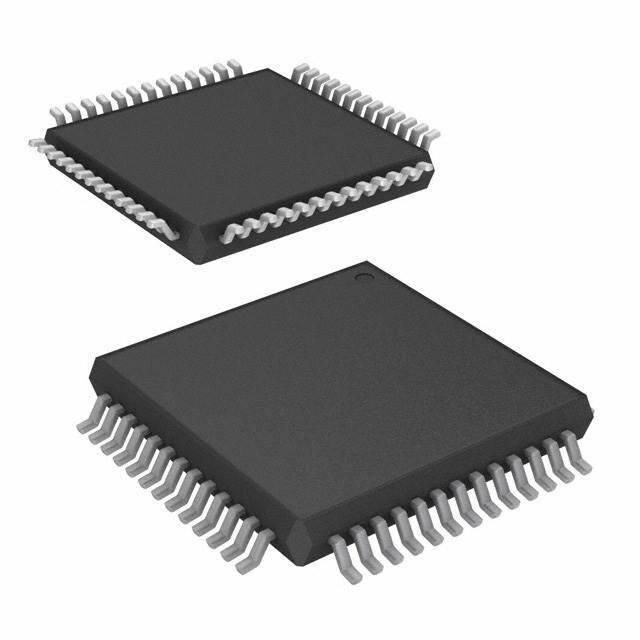


 工商网监
湘ICP备2023018690号
工商网监
湘ICP备2023018690号
