The following document contains information on Cypress products. The document has the series
name, product name, and ordering part numbering with the prefix “MB”. However, Cypress will
offer these products to new and existing customers with the series name, product name, and
ordering part number with the prefix “CY”.
How to Check the Ordering Part Number
1. Go to www.cypress.com/pcn.
2. Enter the keyword (for example, ordering part number) in the SEARCH PCNS field and click
Apply.
3. Click the corresponding title from the search results.
4. Download the Affected Parts List file, which has details of all changes
For More Information
Please contact your local sales office for additional information about Cypress products and
solutions.
About Cypress
Cypress is the leader in advanced embedded system solutions for the world's most innovative
automotive, industrial, smart home appliances, consumer electronics and medical products.
Cypress' microcontrollers, analog ICs, wireless and USB-based connectivity solutions and reliable,
high-performance memories help engineers design differentiated products and get them to market
first. Cypress is committed to providing customers with the best support and development
resources on the planet enabling them to disrupt markets by creating new product categories in
record time. To learn more, go to www.cypress.com.
�MB95650L Series
New 8FX 8-bit Microcontrollers
The MB95650L Series is a series of general-purpose, single-chip microcontrollers. In addition to a compact instruction set, the
microcontrollers of this series contain a variety of peripheral functions.
Features
F2MC-8FX CPU core
I2C bus interface 2 channels (One of the two channels
can be used either as an I2C bus interface channel or
as a UART/SIO channel.)
Instruction set optimized for controllers
■
Multiplication and division instructions
■
16-bit arithmetic operations
■
Bit test branch instructions
■
Bit manipulation instructions, etc.
■
Selectable main clock source
❐ Main oscillation clock (up to 16.25 MHz, maximum machine
clock frequency: 8.125 MHz)
❐ External clock (up to 32.5 MHz, maximum machine clock
frequency: 16.25 MHz)
❐ Main CR clock (4 MHz 2%)
❐ Main CR PLL clock
• The main CR PLL clock frequency becomes 8 MHz 2%
when the PLL multiplication rate is 2.
• The main CR PLL clock frequency becomes 10 MHz 2%
when the PLL multiplication rate is 2.5.
• The main CR PLL clock frequency becomes 12 MHz 2%
when the PLL multiplication rate is 3.
• The main CR PLL clock frequency becomes 16 MHz 2%
when the PLL multiplication rate is 4.
❐ Main PLL clock (maximum machine clock frequency:
16 MHz)
Selectable subclock source
Suboscillation clock (32.768 kHz)
❐ External clock (32.768 kHz)
❐ Sub-CR clock (Typ: 100 kHz, Min: 50 kHz, Max: 150 kHz)
❐
Timer
■
8/16-bit composite timer 2 channels
■
Time-base timer 1 channel
■
Watch prescaler 1 channel
Supports Standard-mode and Fast-mode (400 kHz).
■
Built-in wake-up function
LIN-UART
Clock
■
■
■
Full duplex double buffer
■
Capable of clock asynchronous serial data transfer and clock
synchronous serial data transfer
External interrupt 6 channels
■
Interrupt by edge detection (rising edge, falling edge, and both
edges can be selected)
■
Can be used to wake up the device from different low power
consumption (standby) modes
8/12-bit A/D converter 6 channels
8-bit or 12-bit resolution can be selected.
Low power consumption (standby) modes
There are four standby modes as follows:
■
Stop mode
■
Sleep mode
■
Watch mode
■
Time-base timer mode
I/O port
■
MB95F652E/F653E/F654E/F656E (number of I/O ports: 21)
General-purpose I/O ports (CMOS I/O)
: 17
❐ General-purpose I/O ports (N-ch open drain)
:4
❐
■
MB95F652L/F653L/F654L/F656L (number of I/O ports: 20)
General-purpose I/O ports (CMOS I/O)
: 17
❐ General-purpose I/O ports (N-ch open drain)
:3
❐
UART/SIO 1 channel (The channel can be used either
as a UART/SIO channel or as an I2C bus interface
channel.)
On-chip debug
■
1-wire serial control
■
The function of this channel can be switched between
UART/SIO and I2C bus interface.
■
Serial writing supported (asynchronous mode)
■
Full duplex double buffer
Hardware/software watchdog timer
■
Capable of clock asynchronous (UART) serial data transfer and
clock synchronous (SIO) serial data transfer
■
Built-in hardware watchdog timer
■
Built-in software watchdog timer
Cypress Semiconductor Corporation
Document Number: 002-04696 Rev. *B
•
198 Champion Court
•
San Jose, CA 95134-1709
•
408-943-2600
Revised August 7, 2017
�MB95650L Series
Power-on reset
Clock supervisor counter
A power-on reset is generated when the power is switched on.
Built-in clock supervisor counter
Low-voltage detection reset circuit and low-voltage
detection interrupt circuit (only available on
MB95F652E/F653E/F654E/F656E)
Dual operation Flash memory
Built-in low-voltage detection function
The program/erase operation and the read operation can be
executed in different banks (upper bank/lower bank)
simultaneously.
Flash memory security function
Protects the content of the Flash memory.
Document Number: 002-04696 Rev. *B
Page 2 of 105
�MB95650L Series
Contents
Product Line-up ................................................................ 4
Packages and Corresponding Products ........................ 6
Differences among Products and
Notes on Product Selection ............................................. 7
Pin Assignment ................................................................ 8
Pin Functions .................................................................... 9
I/O Circuit Type ............................................................... 12
Handling Precautions ..................................................... 15
Precautions for Product Design ................................. 15
Precautions for Package Mounting ........................... 16
Precautions for Use Environment .............................. 17
Notes On Device Handling ............................................. 18
Pin Connection ............................................................... 19
Block Diagram ................................................................ 20
CPU Core ......................................................................... 21
Memory Space ................................................................ 22
Areas for Specific Applications .................................... 24
I/O Map ............................................................................. 25
Document Number: 002-04696 Rev. *B
I/O Ports ........................................................................... 29
Port 0 ......................................................................... 30
Port 1 ......................................................................... 36
Port 6 ......................................................................... 42
Port F ......................................................................... 46
Port G ........................................................................ 50
Interrupt Source Table ................................................... 53
Pin States in each Mode ................................................ 54
Electrical Characteristics ............................................... 56
Absolute Maximum Ratings ....................................... 56
Recommended Operating Conditions ....................... 58
DC Characteristics .................................................... 59
AC Characteristics ..................................................... 62
A/D Converter ............................................................ 86
Flash Memory Program/Erase Characteristics .......... 90
Sample Characteristics .................................................. 91
Mask Options .................................................................. 98
Ordering Information ...................................................... 99
Package Dimension ...................................................... 100
Major Changes .............................................................. 103
Document History ......................................................... 104
Page 3 of 105
�MB95650L Series
1. Product Line-up
Part number
MB95F652E MB95F653E MB95F654E MB95F656E MB95F652L MB95F653L MB95F654L MB95F656L
Parameter
Type
Clock supervisor
counter
Flash memory product
It supervises the main clock oscillation and the subclock oscillation.
Flash memory
capacity
8 Kbyte
12 Kbyte
20 Kbyte
36 Kbyte
8 Kbyte
12 Kbyte
20 Kbyte
36 Kbyte
RAM capacity
256 bytes
512 bytes
1024 bytes
1024 bytes
256 bytes
512 bytes
1024 bytes
1024 bytes
Power-on reset
Yes
Low-voltage
detection reset
Reset input
Yes
No
Selected through software
With dedicated reset input
CPU functions
•
•
•
•
•
•
Number of basic instructions
Instruction bit length
Instruction length
Data bit length
Minimum instruction execution time
Interrupt processing time
: 136
: 8 bits
: 1 to 3 bytes
: 1, 8 and 16 bits
: 61.5 ns (machine clock frequency = 16.25 MHz)
: 0.6 µs (machine clock frequency = 16.25 MHz)
General-purpose
I/O
• I/O port
• CMOS I/O
• N-ch open drain
Time-base timer
Interval time: 0.256 ms to 8.3 s (external clock frequency = 4 MHz)
: 21
: 17
:4
• I/O port
• CMOS I/O
• N-ch open drain
: 20
: 17
:3
• Reset generation cycle
Hardware/software
Main oscillation clock at 10 MHz: 105 ms (Min)
watchdog timer
• The sub-CR clock can be used as the source clock of the software watchdog timer.
Wild register
It can be used to replace 3 bytes of data.
LIN-UART
•
•
•
•
8/12-bit
A/D converter
A wide range of communication speed can be selected by a dedicated reload timer.
It has a full duplex double buffer.
Both clock synchronous serial data transfer and clock asynchronous serial data transfer are enabled.
The LIN function can be used as a LIN master or a LIN slave.
6 channels
8-bit or 12-bit resolution can be selected.
2 channels
8/16-bit
composite timer
•
•
•
•
The timer can be configured as an “8-bit timer × 2 channels” or a “16-bit timer × 1 channel”.
It has the following functions: interval timer function, PWC function, PWM function and input capture function.
Count clock: it can be selected from internal clocks (seven types) and external clocks.
It can output square wave.
6 channels
External interrupt
On-chip debug
• Interrupt by edge detection (The rising edge, falling edge, and both edges can be selected.)
• It can be used to wake up the device from different standby modes.
• 1-wire serial control
• It supports serial writing (asynchronous mode).
(Continued)
Document Number: 002-04696 Rev. *B
Page 4 of 105
�MB95650L Series
(Continued)
Part number
MB95F652E MB95F653E MB95F654E MB95F656E MB95F652L MB95F653L MB95F654L MB95F656L
Parameter
1 channel (The channel can be used either as a UART/SIO channel or as an I2C bus interface channel.)
UART/SIO
I2C bus
interface
• Data transfer with UART/SIO is enabled.
• It has a full duplex double buffer, variable data length (5/6/7/8 bits), an internal baud rate generator and an
error detection function.
• It uses the NRZ type transfer format.
• LSB-first data transfer and MSB-first data transfer are available to use.
• Both clock asynchronous (UART) serial data transfer and clock synchronous (SIO) serial data transfer are
enabled.
2 channels (One of the two channels can be used either as an I2C bus interface channel or as a UART/SIO
channel.)
• Master/slave transmission and reception
• It has the following functions: bus error function, arbitration function, transmission direction detection function,
wake-up function, and functions of generating and detecting repeated START conditions.
Watch prescaler
Eight different time intervals can be selected.
Flash memory
• It supports automatic programming (Embedded Algorithm), and program/erase/erase-suspend/erase-resume
commands.
• It has a flag indicating the completion of the operation of Embedded Algorithm.
• Flash security feature for protecting the content of the Flash memory
Number of program/erase cycles
Data retention time
Standby mode
1000
20 years
10000
10 years
100000
5 years
There are four standby modes as follows:
• Stop mode
• Sleep mode
• Watch mode
• Time-base timer mode
Package
Document Number: 002-04696 Rev. *B
FPT-24P-M10
FPT-24P-M34
LCC-32P-M19
Page 5 of 105
�MB95650L Series
2. Packages and Corresponding Products
Part number
MB95F652E MB95F653E MB95F654E MB95F656E MB95F652L MB95F653L MB95F654L MB95F656L
Package
FPT-24P-M10
FPT-24P-M34
LCC-32P-M19
: Available
Document Number: 002-04696 Rev. *B
Page 6 of 105
�MB95650L Series
3. Differences among Products and Notes on Product Selection
Current consumption
When using the on-chip debug function, take account of the current consumption of Flash memory program/erase.
For details of current consumption, see “18. Electrical Characteristics”.
Package
For details of information on each package, see “2. Packages and Corresponding Products” and “22. Package Dimension”.
Operating voltage
The operating voltage varies, depending on whether the on-chip debug function is used or not.
For details of operating voltage, see “18. Electrical Characteristics”.
On-chip debug function
The on-chip debug function requires that VCC, VSS and one serial wire be connected to an evaluation tool. For details of the connection
method, refer to “Chapter 20 Example Of Serial Programming Connection” in “New 8FX MB95650L Series Hardware Manual”.
Document Number: 002-04696 Rev. *B
Page 7 of 105
�MB95650L Series
4. Pin Assignment
PF0/X0
PF1/X1
Vss
PG2/X1A
PG1/X0A
24
23
P12/DBG/EC0
P07/INT07/TO10
3
4
(TOP VIEW)
22
21
P06/INT06/TO01
P05/INT05/AN05/TO00
5
6
TSSOP24
FPT-24P-M10
20
19
P04/INT04/AN04/SIN/EC0
P03/INT03/AN03/SOT
18
P02/INT02/AN02/SCK
17
P01/AN01
16
P00/AN00
15
P64/EC1
14
P14/SDA0
13
P15/SCL0
7
8
9
10
11
12
SOP24
FPT-24P-M34
32
31
30
29
28
27
26
25
PF0/X0
PF1/X1
NC
NC
NC
NC
P07/INT07/TO10
P12/DBG/EC0
Vcc
C
PF2/RST
P17/SCL1/UI0
P16/SDA1/UO0
P62/TO10/UCK0
P63/TO11
1
2
Vss
PG2/X1A
1
2
PG1/X0A
Vcc
3
4
C
5
6
Document Number: 002-04696 Rev. *B
QFN32
LCC-32P-M19
9
10
11
12
13
14
15
16
P15/SCL0
7
8
P63/TO11
P62/TO10/UCK0
NC
NC
NC
NC
P14/SDA0
PF2/RST
P17/SCL1/UI0
P16/SDA1/UO0
(TOP VIEW)
24
23
22
21
P06/INT06/TO01
P05/INT05/AN05/TO00
P04/INT04/AN04/SIN/EC0
P03/INT03/AN03/SOT
20
19
18
17
P02/INT02/AN02/SCK
P01/AN01
P00/AN00
P64/EC1
Page 8 of 105
�MB95650L Series
5. Pin Functions
Pin no.
SOP24*1,
TSSOP24*2
QFN32*3
1
32
2
31
3
1
Pin name
PF0
X0
PF1
X1
VSS
PG2
I/O
circuit
type*4
B
B
—
General-purpose I/O port
Main clock input oscillation pin
General-purpose I/O port
Main clock I/O oscillation pin
Power supply pin (GND)
General-purpose I/O port
Input
Output
OD*5
PU*6
Hysteresis
CMOS
—
—
Hysteresis
CMOS
—
—
—
—
—
—
Hysteresis
CMOS
—
Hysteresis
CMOS
—
4
2
5
3
6
4
VCC
—
Power supply pin
—
—
—
—
7
5
C
—
Decoupling capacitor connection pin
—
—
—
—
Hysteresis
CMOS
—
CMOS
CMOS
—/*7
—
CMOS
CMOS
—/*7
—
Hysteresis
CMOS
—
Hysteresis
CMOS
—
CMOS
CMOS
—
CMOS
CMOS
—
Hysteresis
CMOS
—
X1A
PG1
X0A
C
I/O type
Function
C
PF2
8
6
RST
10
11
7
8
10
SCL1
A
9
J
16
14
15
15
17
Reset pin
Dedicated reset pin on
MB95F652L/F653L/F654L/F656L
I2C bus interface ch. 1 clock I/O pin
UI0
UART/SIO ch. 0 data input pin
P16
General-purpose I/O port
SDA1
J
I2C bus interface ch. 1 data I/O pin
UO0
UART/SIO ch. 0 data output pin
P62
General-purpose I/O port
High-current pin
TO10
D
P63
P15
SCL0
P14
SDA0
D
General-purpose I/O port
High-current output
8/16-bit composite timer ch. 1 output pin
I
I
P64
EC1
8/16-bit composite timer ch. 1 output pin
UART/SIO ch. 0 clock I/O pin
TO11
13
Subclock input oscillation pin
General-purpose I/O port
UCK0
12
General-purpose I/O port
General-purpose I/O port
P17
9
Subclock I/O oscillation pin
General-purpose I/O port
I2C bus interface ch. 0 clock I/O pin
General-purpose I/O port
I2C bus interface ch. 0 data I/O pin
General-purpose I/O port
D
8/16-bit composite timer ch. 1 clock input
pin
(Continued)
Document Number: 002-04696 Rev. *B
Page 9 of 105
�MB95650L Series
Pin no.
SOP24*1,
TSSOP24*2
QFN32*3
16
18
17
18
Pin name
P00
AN00
P01
AN01
I/O
circuit
type*4
E
E
P02
18
19
20
21
20
21
22
23
INT02
AN02
24
E
General-purpose I/O port
8/12-bit A/D converter analog input pin
External interrupt input pin
8/12-bit A/D converter analog input pin
LIN-UART clock I/O pin
P03
General-purpose I/O port
INT03
AN03
E
External interrupt input pin
8/12-bit A/D converter analog input pin
SOT
LIN-UART data output pin
P04
General-purpose I/O port
INT04
External interrupt input pin
AN04
8/12-bit A/D converter analog input pin
SIN
F
LIN-UART data input pin
EC0
8/16-bit composite timer ch. 0 clock input
pin
P05
General-purpose I/O port
High-current pin
INT05
K
External interrupt input pin
AN05
8/12-bit A/D converter analog input pin
TO00
8/16-bit composite timer ch. 0 output pin
INT06
D
INT07
TO10
Output
OD*5
PU*6
Hysteresis/
analog
CMOS
—
Hysteresis/
analog
CMOS
—
Hysteresis/
analog
CMOS
—
Hysteresis/
analog
CMOS
—
CMOS/
analog
CMOS
—
Hysteresis/
analog
CMOS
—
General-purpose I/O port
High-current pin
External interrupt input pin
Hysteresis
CMOS
—
Hysteresis
CMOS
—
8/16-bit composite timer ch. 0 output pin
P07
26
8/12-bit A/D converter analog input pin
SCK
TO01
23
General-purpose I/O port
Input
General-purpose I/O port
P06
22
I/O type
Function
K
General-purpose I/O port
High-current pin
External interrupt input pin
8/16-bit composite timer ch. 1 output pin
(Continued)
Document Number: 002-04696 Rev. *B
Page 10 of 105
�MB95650L Series
(Continued)
Pin no.
1
SOP24* ,
TSSOP24*2
QFN32*3
Pin name
P12
24
25
DBG
I/O type
I/O
circuit
type*4
Function
Input
Output
OD*5
PU*6
Hysteresis
CMOS
—
—
—
—
—
General-purpose I/O port
H
EC0
DBG input pin
8/16-bit composite timer ch. 0 clock input
pin
11
12
13
—
14
27
NC
—
It is an internally connected pin. Always
leave it unconnected.
28
29
30
: Available
*1: FPT-24P-M34
*2: FPT-24P-M10
*3: LCC-32P-M19
*4: For the I/O circuit types, see “6. I/O Circuit Type”.
*5: N-ch open drain
*6: Pull-up
*7: In I2C mode, the pin becomes an N-ch open drain pin.
Document Number: 002-04696 Rev. *B
Page 11 of 105
�MB95650L Series
6. I/O Circuit Type
Type
Circuit
Remarks
Reset input / Hysteresis input
A
Reset output / Digital output
• N-ch open drain output
• Hysteresis input
• Reset output
N-ch
P-ch
Port select
Digital output
N-ch
Digital output
Standby control
Hysteresis input
Clock input
X1
B
X0
• CMOS output
• Hysteresis input
Standby control / Port select
P-ch
• Oscillation circuit
• High-speed side
Feedback resistance:
approx. 1 M
Port select
Digital output
N-ch
Digital output
Standby control
Hysteresis input
Port select
R
Pull-up control
P-ch
P-ch
Digital output
N-ch
Digital output
Standby control
Hysteresis input
Clock input
X1A
C
• Oscillation circuit
• Low-speed side
Feedback resistance:
approx. 5 M
• CMOS output
• Hysteresis input
• Pull-up control
X0A
Standby control / Port select
Port select
R
Pull-up control
Digital output
P-ch
Digital output
N-ch
Digital output
Standby control
Hysteresis input
(Continued)
Document Number: 002-04696 Rev. *B
Page 12 of 105
�MB95650L Series
Type
Circuit
Remarks
Pull-up control
R
P-ch
D
Digital output
P-ch
Digital output
N-ch
•
•
•
•
CMOS output
Hysteresis input
Pull-up control
High current output
•
•
•
•
CMOS output
Hysteresis input
Pull-up control
Analog input
•
•
•
•
CMOS output
CMOS input
Pull-up control
Analog input
Standby control
Hysteresis input
Pull-up control
R
P-ch
Digital output
P-ch
Digital output
E
N-ch
Analog input
A/D control
Standby control
Hysteresis input
Pull-up control
R
P-ch
Digital output
P-ch
F
Digital output
N-ch
Analog input
A/D control
Standby control
CMOS input
Standby control
Hysteresis input
H
• N-ch open drain output
• Hysteresis input
Digital output
N-ch
Digital output
I
N-ch
Standby control
• N-ch open drain output
• CMOS input
CMOS input
(Continued)
Document Number: 002-04696 Rev. *B
Page 13 of 105
�MB95650L Series
(Continued)
Type
Circuit
Remarks
I2C mode control
Digital output
J
P-ch
Digital output
• CMOS output
• CMOS input
• N-ch open drain output in I2C mode
N-ch
Standby control
CMOS input
Pull-up control
R
P-ch
Digital output
P-ch
K
Digital output
N-ch
Analog input
•
•
•
•
•
CMOS output
Hysteresis input
Pull-up control
Analog input
High current output
A/D control
Standby control
Hysteresis input
Document Number: 002-04696 Rev. *B
Page 14 of 105
�MB95650L Series
7. Handling Precautions
Any semiconductor devices have inherently a certain rate of failure. The possibility of failure is greatly affected by the conditions in
which they are used (circuit conditions, environmental conditions, etc.). This page describes precautions that must be observed to
minimize the chance of failure and to obtain higher reliability from your Cypress semiconductor devices.
7.1 Precautions for Product Design
This section describes precautions when designing electronic equipment using semiconductor devices.
Absolute Maximum Ratings
Semiconductor devices can be permanently damaged by application of stress (voltage, current, temperature, etc.) in excess of certain
established limits, called absolute maximum ratings. Do not exceed these ratings.
Recommended Operating Conditions
Recommended operating conditions are normal operating ranges for the semiconductor device. All the device's electrical characteristics are warranted when operated within these ranges.
Always use semiconductor devices within the recommended operating conditions. Operation outside these ranges may adversely
affect reliability and could result in device failure.
No warranty is made with respect to uses, operating conditions, or combinations not represented on the data sheet. Users considering
application outside the listed conditions are advised to contact their sales representative beforehand.
Processing and Protection of Pins
These precautions must be followed when handling the pins which connect semiconductor devices to power supply and input/output
functions.
1. Preventing Over-Voltage and Over-Current Conditions
Exposure to voltage or current levels in excess of maximum ratings at any pin is likely to cause deterioration within the device, and
in extreme cases leads to permanent damage of the device. Try to prevent such overvoltage or over-current conditions at the
design stage.
2. Protection of Output Pins
Shorting of output pins to supply pins or other output pins, or connection to large capacitance can cause large current flows. Such
conditions if present for extended periods of time can damage the device.
Therefore, avoid this type of connection.
3. Handling of Unused Input Pins
Unconnected input pins with very high impedance levels can adversely affect stability of operation. Such pins should be connected
through an appropriate resistance to a power supply pin or ground pin.
Latch-up
Semiconductor devices are constructed by the formation of P-type and N-type areas on a substrate. When subjected to abnormally
high voltages, internal parasitic PNPN junctions (called thyristor structures) may be formed, causing large current levels in excess of
several hundred mA to flow continuously at the power supply pin. This condition is called latch-up.
CAUTION: The occurrence of latch-up not only causes loss of reliability in the semiconductor device, but can cause injury or damage
from high heat, smoke or flame. To prevent this from happening, do the following:
1. Be sure that voltages applied to pins do not exceed the absolute maximum ratings. This should include attention to abnormal noise,
surge levels, etc.
2. Be sure that abnormal current flows do not occur during the power-on sequence.
Observance of Safety Regulations and Standards
Most countries in the world have established standards and regulations regarding safety, protection from electromagnetic interference,
etc. Customers are requested to observe applicable regulations and standards in the design of products.
Fail-Safe Design
Any semiconductor devices have inherently a certain rate of failure. You must protect against injury, damage or loss from such failures
by incorporating safety design measures into your facility and equipment such as redundancy, fire protection, and prevention of
over-current levels and other abnormal operating conditions.
Document Number: 002-04696 Rev. *B
Page 15 of 105
�MB95650L Series
Precautions Related to Usage of Devices
Cypress semiconductor devices are intended for use in standard applications (computers, office automation and other office
equipment, industrial, communications, and measurement equipment, personal or household devices, etc.).
CAUTION: Customers considering the use of our products in special applications where failure or abnormal operation may directly
affect human lives or cause physical injury or property damage, or where extremely high levels of reliability are demanded (such as
aerospace systems, atomic energy controls, sea floor repeaters, vehicle operating controls, medical devices for life support, etc.) are
requested to consult with sales representatives before such use. The company will not be responsible for damages arising from such
use without prior approval.
7.2 Precautions for Package Mounting
Package mounting may be either lead insertion type or surface mount type. In either case, for heat resistance during soldering, you
should only mount under Cypress’s recommended conditions. For detailed information about mount conditions, contact your sales
representative.
Lead Insertion Type
Mounting of lead insertion type packages onto printed circuit boards may be done by two methods: direct soldering on the board, or
mounting by using a socket.
Direct mounting onto boards normally involves processes for inserting leads into through-holes on the board and using the flow
soldering (wave soldering) method of applying liquid solder. In this case, the soldering process usually causes leads to be subjected
to thermal stress in excess of the absolute ratings for storage temperature. Mounting processes should conform to Cypress
recommended mounting conditions.
If socket mounting is used, differences in surface treatment of the socket contacts and IC lead surfaces can lead to contact
deterioration after long periods. For this reason it is recommended that the surface treatment of socket contacts and IC leads be
verified before mounting.
Surface Mount Type
Surface mount packaging has longer and thinner leads than lead-insertion packaging, and therefore leads are more easily deformed
or bent. The use of packages with higher pin counts and narrower pin pitch results in increased susceptibility to open connections
caused by deformed pins, or shorting due to solder bridges.
You must use appropriate mounting techniques. Cypress recommends the solder reflow method, and has established a ranking of
mounting conditions for each product. Users are advised to mount packages in accordance with Cypress ranking of recommended
conditions.
Lead-Free Packaging
CAUTION: When ball grid array (BGA) packages with Sn-Ag-Cu balls are mounted using Sn-Pb eutectic soldering, junction strength
may be reduced under some conditions of use.
Storage of Semiconductor Devices
Because plastic chip packages are formed from plastic resins, exposure to natural environmental conditions will cause absorption of
moisture. During mounting, the application of heat to a package that has absorbed moisture can cause surfaces to peel, reducing
moisture resistance and causing packages to crack. To prevent, do the following:
1. Avoid exposure to rapid temperature changes, which cause moisture to condense inside the product. Store products in locations
where temperature changes are slight.
2. Use dry boxes for product storage. Products should be stored below 70% relative humidity, and at temperatures between 5°C and
30°C.
When you open Dry Package that recommends humidity 40% to 70% relative humidity.
3. When necessary, Cypress packages semiconductor devices in highly moisture-resistant aluminum laminate bags, with a silica gel
desiccant. Devices should be sealed in their aluminum laminate bags for storage.
4. Avoid storing packages where they are exposed to corrosive gases or high levels of dust.
Baking
Packages that have absorbed moisture may be de-moisturized by baking (heat drying). Follow the Cypress recommended conditions
for baking.
Condition: 125°C/24 h
Document Number: 002-04696 Rev. *B
Page 16 of 105
�MB95650L Series
Static Electricity
Because semiconductor devices are particularly susceptible to damage by static electricity, you must take the following precautions:
1. Maintain relative humidity in the working environment between 40% and 70%.
Use of an apparatus for ion generation may be needed to remove electricity.
2. Electrically ground all conveyors, solder vessels, soldering irons and peripheral equipment.
3. Eliminate static body electricity by the use of rings or bracelets connected to ground through high resistance (on the level of 1 MΩ).
Wearing of conductive clothing and shoes, use of conductive floor mats and other measures to minimize shock loads is
recommended.
4. Ground all fixtures and instruments, or protect with anti-static measures.
5. Avoid the use of styrofoam or other highly static-prone materials for storage of completed board assemblies.
7.3 Precautions for Use Environment
Reliability of semiconductor devices depends on ambient temperature and other conditions as described above.
For reliable performance, do the following:
1. Humidity
Prolonged use in high humidity can lead to leakage in devices as well as printed circuit boards. If high humidity levels are
anticipated, consider anti-humidity processing.
2. Discharge of Static Electricity
When high-voltage charges exist close to semiconductor devices, discharges can cause abnormal operation. In such cases, use
anti-static measures or processing to prevent discharges.
3. Corrosive Gases, Dust, or Oil
Exposure to corrosive gases or contact with dust or oil may lead to chemical reactions that will adversely affect the device. If you
use devices in such conditions, consider ways to prevent such exposure or to protect the devices.
4. Radiation, Including Cosmic Radiation
Most devices are not designed for environments involving exposure to radiation or cosmic radiation. Users should provide shielding
as appropriate.
5. Smoke, Flame
CAUTION: Plastic molded devices are flammable, and therefore should not be used near combustible substances. If devices begin
to smoke or burn, there is danger of the release of toxic gases.
Customers considering the use of Cypress products in other special environmental conditions should consult with sales
representatives.
Document Number: 002-04696 Rev. *B
Page 17 of 105
�MB95650L Series
8. Notes On Device Handling
Preventing latch-ups
When using the device, ensure that the voltage applied does not exceed the maximum voltage rating.
In a CMOS IC, if a voltage higher than VCC or a voltage lower than VSS is applied to an input/output pin that is neither a
medium-withstand voltage pin nor a high-withstand voltage pin, or if a voltage out of the rating range of power supply voltage mentioned
in “18.1 Absolute Maximum Ratings” of “18. Electrical Characteristics” is applied to the VCC pin or the VSS pin, a latch-up may occur.
When a latch-up occurs, power supply current increases significantly, which may cause a component to be thermally destroyed.
Stabilizing supply voltage
Supply voltage must be stabilized.
A malfunction may occur when power supply voltage fluctuates rapidly even though the fluctuation is within the guaranteed operating
range of the VCC power supply voltage.
As a rule of voltage stabilization, suppress voltage fluctuation so that the fluctuation in VCC ripple (p-p value) at the commercial
frequency (50 Hz/60 Hz) does not exceed 10% of the standard VCC value, and the transient fluctuation rate does not exceed 0.1 V/ms
at a momentary fluctuation such as switching the power supply.
Notes on using the external clock
When an external clock is used, oscillation stabilization wait time is required for power-on reset, wake-up from subclock mode or stop
mode.
Document Number: 002-04696 Rev. *B
Page 18 of 105
�MB95650L Series
9. Pin Connection
Treatment of unused pins
If an unused input pin is left unconnected, a component may be permanently damaged due to malfunctions or latch-ups. Always pull
up or pull down an unused input pin through a resistor of at least 2 k. Set an unused input/output pin to the output state and leave
it unconnected, or set it to the input state and treat it the same as an unused input pin. If there is an unused output pin, leave it
unconnected.
Power supply pins
To reduce unnecessary electro-magnetic emission, prevent malfunctions of strobe signals due to an increase in the ground level, and
conform to the total output current standard, always connect the VCC pin and the VSS pin to the power supply and ground outside the
device. In addition, connect the current supply source to the VCC pin and the VSS pin with low impedance.
It is also advisable to connect a ceramic capacitor of approximately 1.0 µF as a bypass capacitor between the VCC pin and the VSS
pin at a location close to this device.
DBG pin
Connect the DBG pin to an external pull-up resistor of 2 k or above.
After power-on, ensure that the DBG pin does not stay at “L” level until the reset output is released.
The DBG pin becomes a communication pin in debug mode. Since the actual pull-up resistance depends on the tool used and the
interconnection length, refer to the tool document when selecting a pull-up resistor.
RST pin
Connect the RST pin to an external pull-up resistor of 2 k or above.
To prevent the device from unintentionally entering the reset mode due to noise, minimize the interconnection length between a pull-up
resistor and the RST pin and that between a pull-up resistor and the VCC pin when designing the layout of the printed circuit board.
The PF2/RST pin functions as the reset input/output pin after power-on. In addition, the reset output of the PF2/RST pin can be enabled
by the RSTOE bit in the SYSC register, and the reset input function and the general purpose I/O function can be selected by the
RSTEN bit in the SYSC register.
C pin
Use a ceramic capacitor or a capacitor with equivalent frequency characteristics. The decoupling capacitor for the VCC pin must have
a capacitance equal to or larger than the capacitance of CS. For the connection to a decoupling capacitor CS, see the diagram below.
To prevent the device from unintentionally entering a mode to which the device is not set to transit due to noise, minimize the distance
between the C pin and CS and the distance between CS and the VSS pin when designing the layout of a printed circuit board.
DBG/RST/C pins connection diagram
DBG
C
RST
Cs
Note on serial communication
In serial communication, reception of wrong data may occur due to noise or other causes. Therefore, design a printed circuit board
to prevent noise from occurring. Taking account of the reception of wrong data, take measures such as adding a checksum to the end
of data in order to detect errors. If an error is detected, retransmit the data.
Document Number: 002-04696 Rev. *B
Page 19 of 105
�MB95650L Series
10. Block Diagram
F2MC-8FX CPU
PF2*1/RST*2
Reset with LVD
Dual operation Flash with
security function
(36/20/12/8 Kbyte)
PF0/X0*2
PF1/X1*2
PG1/X0A*2
Oscillator
circuit
CR oscillator
RAM (1024/512/256 bytes)
PG2/X1A*2
(P05/TO00)
Clock control
8/16-bit composite timer ch. 0
(P06/TO01)
(P04/EC0), P12*1/EC0
On-chip debug
Wild register
P02/INT02 to P07/INT07
External interrupt
C
(P00/AN00 to P05*3/AN05)
(P62*3/TO10), P62*3/TO10
8/16-bit composite timer ch. 1
P63*3/TO11
P64/EC1
I2C bus interface ch. 0
8/12-bit A/D converter
I2C bus interface ch. 1
(P04/SIN)
(P03/SOT)
Internal bus
(P12*1/DBG)
P14*1/SDA0
P15*1/SCL0
(P16/SDA1)
(P17/SCL1)
LIN-UART
(P02/SCK)
P17/UI0
UART/SIO ch. 0
P16/UO0
P62/UCK0
Port
Port
Vcc
Vss
*1: P12, P14, P15 and PF2 are N-ch open drain pins.
*2: Software select
*3: P05 to P07, P62 and P63 are high-current pins.
Note: Pins in parentheses indicate that those pins are shared among different peripheral functions.
Document Number: 002-04696 Rev. *B
Page 20 of 105
�MB95650L Series
11. CPU Core
Memory space
The memory space of the MB95650L Series is 64 Kbyte in size, and consists of an I/O area, an extended I/O area, a data area, and
a program area. The memory space includes areas intended for specific purposes such as general-purpose registers and a vector
table. The memory maps of the MB95650L Series are shown below.
Memory maps
MB95F652E/F652L
0x0000
0x0080
0x0090
0x0100
0x0190
I/O area
Access prohibited
RAM 256 bytes
Registers
MB95F653E/F653L
0x0000
0x0080
0x0090
0x0100
0x0200
I/O area
Access prohibited
RAM 512 bytes
Registers
MB95F654E/F654L
0x0000
0x0080
0x0090
0x0100
0x0200
I/O area
Access prohibited
RAM 1024 bytes
Registers
MB95F656E/F656L
0x0000
0x0080
0x0090
0x0100
0x0200
I/O area
Access prohibited
RAM 1024 bytes
Registers
0x0290
Access prohibited
Access prohibited
0x0490
0x0490
Access prohibited
0x0F80
0x0F80
0x0F80
Flash memory 4 Kbyte
Flash memory 4 Kbyte
Flash memory 4 Kbyte
0x2000
0x2000
0x2000
0x2000
Extended I/O area
0x1000
0x1000
0x1000
Flash memory 4 Kbyte
0x0F80
Extended I/O area
Extended I/O area
Extended I/O area
0x1000
Access prohibited
Access prohibited
Access prohibited
0x8000
Access prohibited
Access prohibited
0xC000
Flash memory 32 Kbyte
Flash memory 16 Kbyte
0xE000
Flash memory 8 Kbyte
0xF000
Flash memory 4 Kbyte
0xFFFF
0xFFFF
Document Number: 002-04696 Rev. *B
0xFFFF
0xFFFF
Page 21 of 105
�MB95650L Series
12. Memory Space
The memory space of the MB95650L Series is 64 Kbyte in size, and consists of an I/O area, an extended I/O area, a data area, and
a program area. The memory space includes areas for specific applications such as general-purpose registers and a vector table.
I/O area (addresses: 0x0000 to 0x007F)
• This area contains the control registers and data registers for built-in peripheral functions.
• As the I/O area forms part of the memory space, it can be accessed in the same way as the memory. It can also be accessed
at high-speed by using direct addressing instructions.
Extended I/O area (addresses: 0x0F80 to 0x0FFF)
• This area contains the control registers and data registers for built-in peripheral functions.
• As the extended I/O area forms part of the memory space, it can be accessed in the same way as the memory.
Data area
•
•
•
•
•
•
•
•
•
Static RAM is incorporated in the data area as the internal data area.
The internal RAM size varies according to product.
The RAM area from 0x0090 to 0x00FF can be accessed at high-speed by using direct addressing instructions.
In MB95F656E/F656L, the area from 0x0090 to 0x047F is an extended direct addressing area. It can be accessed at high-speed
by direct addressing instructions with a direct bank pointer set.
In MB95F654E/F654L, the area from 0x0090 to 0x047F is an extended direct addressing area. It can be accessed at high-speed
by direct addressing instructions with a direct bank pointer set.
In MB95F653E/F653L, the area from 0x0090 to 0x028F is an extended direct addressing area. It can be accessed at high-speed
by direct addressing instructions with a direct bank pointer set.
In MB95F652E/F652L, the area from 0x0090 to 0x018F is an extended direct addressing area. It can be accessed at high-speed
by direct addressing instructions with a direct bank pointer set.
In MB95F653E/F653L/F654E/F654L/F656E/F656L, the area from 0x0100 to 0x01FF can be used as a general-purpose register
area.
In MB95F652E/F652L, the area from 0x0100 to 0x018F can be used as a general-purpose register area.
Program area
•
•
•
•
The Flash memory is incorporated in the program area as the internal program area.
The Flash memory size varies according to product.
The area from 0xFFC0 to 0xFFFF is used as the vector table.
The area from 0xFFBB to 0xFFBF is used to store data of the non-volatile register.
Document Number: 002-04696 Rev. *B
Page 22 of 105
�MB95650L Series
Memory space map
0x0000
0x0080
0x0090
0x0100
I/O area
Direct addressing area
Access prohibited
Registers
(General-purpose register area)
Extended direct addressing area
0x0200
Data area
0x047F
0x048F
0x0490
Access prohibited
0x0F80
0x0FFF
0x1000
Extended I/O area
Program area
0xFFC0
0xFFFF
Document Number: 002-04696 Rev. *B
Vector table area
Page 23 of 105
�MB95650L Series
13. Areas for Specific Applications
The general-purpose register area and vector table area are used for the specific applications.
General-purpose register area (Addresses: 0x0100 to 0x01FF*1)
• This area contains the auxiliary registers used for 8-bit arithmetic operations, transfer, etc.
• As this area forms part of the RAM area, it can also be used as conventional RAM.
• When the area is used as general-purpose registers, general-purpose register addressing enables high-speed access with short
instructions.
Non-volatile register data area (Addresses: 0xFFBB to 0xFFBF)
• The area from 0xFFBB to 0xFFBF is used to store data of the non-volatile register. For details, refer to “Chapter 23 Non-volatile
Register (NVR) Interface” in “New 8FX MB95650L Series Hardware Manual”.
Vector table area (Addresses: 0xFFC0 to 0xFFFF)
• This area is used as the vector table for vector call instructions (CALLV), interrupts, and resets.
• The top of the Flash memory area is allocated to the vector table area. The start address of a service routine is set to an address
in the vector table in the form of data.
“16. Interrupt Source Table” lists the vector table addresses corresponding to vector call instructions, interrupts, and resets.
For details, refer to “Chapter 4 Reset”, “Chapter 5 Interrupts” and “A.2 Special Instruction Special Instruction CALLV #vct” in “New
8FX MB95650L Series Hardware Manual”.
Direct bank pointer and access area
Direct bank pointer (DP[2:0])
Operand-specified dir
Access area
0bXXX (It does not affect mapping.)
0x0000 to 0x007F
0x0000 to 0x007F
0b000 (Initial value)
0x0090 to 0x00FF
0x0090 to 0x00FF
0b001
0x0100 to 0x017F
0b010
0x0180 to 0x01FF*1
0b011
0b100
0x0200 to 0x027F
0x0080 to 0x00FF
0x0280 to 0x02FF*2
0b101
0x0300 to 0x037F
0b110
0x0380 to 0x03FF
0b111
0x0400 to 0x047F
*1: Due to the memory size limit, the available access area is up to “0x018F” in MB95F652E/F652L.
*2: Due to the memory size limit, the available access area is up to “0x028F” in MB95F653E/F653L.
Document Number: 002-04696 Rev. *B
Page 24 of 105
�MB95650L Series
14. I/O Map
Address
Register
abbreviation
0x0000
PDR0
0x0001
0x0002
0x0003
R/W
Initial value
Port 0 data register
R/W
0b00000000
DDR0
Port 0 direction register
R/W
0b00000000
PDR1
Port 1 data register
R/W
0b00000000
DDR1
Port 1 direction register
R/W
0b00000000
0x0004
—
0x0005
WATR
Register name
—
—
Oscillation stabilization wait time setting register
(Disabled)
R/W
0b11111111
0x0006
PLLC
PLL control register
R/W
0b000X0000
0x0007
SYCC
System clock control register
R/W
0bXXX11011
0x0008
STBC
Standby control register
R/W
0b00000000
0x0009
RSRR
Reset source register
R/W
0b000XXXXX
0x000A
TBTC
Time-base timer control register
R/W
0b00000000
0x000B
WPCR
Watch prescaler control register
R/W
0b00000000
0x000C
WDTC
Watchdog timer control register
R/W
0b00XX0000
0x000D
SYCC2
System clock control register 2
R/W
0bXXXX0011
0x000E
to
0x0015
—
—
—
0x0016
PDR6
Port 6 data register
R/W
0b00000000
0x0017
DDR6
Port 6 direction register
R/W
0b00000000
0x0018
to
0x0027
—
—
—
0x0028
PDRF
Port F data register
R/W
0b00000000
0x0029
DDRF
Port F direction register
R/W
0b00000000
(Disabled)
(Disabled)
0x002A
PDRG
Port G data register
R/W
0b00000000
0x002B
DDRG
Port G direction register
R/W
0b00000000
0x002C
PUL0
Port 0 pull-up register
R/W
0b00000000
0x002D
to
0x0032
—
—
—
0x0033
PUL6
R/W
0b00000000
0x0034
—
—
—
(Disabled)
Port 6 pull-up register
(Disabled)
0x0035
PULG
Port G pull-up register
R/W
0b00000000
0x0036
T01CR1
8/16-bit composite timer 01 status control register 1
R/W
0b00000000
0x0037
T00CR1
8/16-bit composite timer 00 status control register 1
R/W
0b00000000
0x0038
T11CR1
8/16-bit composite timer 11 status control register 1
R/W
0b00000000
0x0039
T10CR1
8/16-bit composite timer 10 status control register 1
R/W
0b00000000
0x003A
to
0x0048
—
—
—
(Disabled)
(Continued)
Document Number: 002-04696 Rev. *B
Page 25 of 105
�MB95650L Series
Address
Register
abbreviation
0x0049
EIC10
0x004A
0x004B
0x004C
to
0x004E
—
0x004F
LVDC
0x0050
0x0051
0x0052
0x0053
0x0054
Register name
R/W
Initial value
External interrupt circuit control register ch. 2/ch. 3
R/W
0b00000000
EIC20
External interrupt circuit control register ch. 4/ch. 5
R/W
0b00000000
EIC30
External interrupt circuit control register ch. 6/ch. 7
R/W
0b00000000
—
—
LVD control register
R/W
0b00000100
SCR
LIN-UART serial control register
R/W
0b00000000
SMR
LIN-UART serial mode register
R/W
0b00000000
R/W
0b00001000
R/W
0b00000000
(Disabled)
SSR
LIN-UART serial status register
RDR
LIN-UART receive data register
TDR
LIN-UART transmit data register
ESCR
LIN-UART extended status control register
R/W
0b00000100
0x0055
ECCR
LIN-UART extended communication control register
R/W
0b000000XX
0x0056
SMC10
UART/SIO serial mode control register 1 ch. 0
R/W
0b00000000
0x0057
SMC20
UART/SIO serial mode control register 2 ch. 0
R/W
0b00100000
0x0058
SSR0
UART/SIO serial status and data register ch. 0
R/W
0b00000001
R/W
0b00000000
R
0b00000000
—
—
R/W
0b00000000
0x0059
TDR0
UART/SIO serial output data register ch. 0
0x005A
RDR0
UART/SIO serial input data register ch. 0
0x005B
to
0x005F
—
0x0060
IBCR00
0x0061
0x0062
IBCR10
IBSR0
(Disabled)
I2C bus control register 0 ch. 0
I
2C
bus control register 1 ch. 0
R/W
0b00000000
I
2C
bus status register ch. 0
R/W
0b00000000
2C
0x0063
IDDR0
I
data register ch. 0
R/W
0b00000000
0x0064
IAAR0
I2C address register ch. 0
R/W
0b00000000
0x0065
0x0066
ICCR0
IBCR01
I
2C
clock control register ch. 0
R/W
0b00000000
I
2C
bus control register 0 ch. 1
R/W
0b00000000
2C
bus control register 1 ch. 1
R/W
0b00000000
R/W
0b00000000
0x0067
IBCR11
I
0x0068
IBSR1
I2C bus status register ch. 1
0x0069
0x006A
IDDR1
IAAR1
I
2C
data register ch. 1
R/W
0b00000000
I
2C
address register ch. 1
R/W
0b00000000
2C
clock control register ch. 1
0x006B
ICCR1
I
R/W
0b00000000
0x006C
ADC1
8/12-bit A/D converter control register 1
R/W
0b00000000
0x006D
ADC2
8/12-bit A/D converter control register 2
R/W
0b00000000
0x006E
ADDH
8/12-bit A/D converter data register (upper)
R/W
0b00000000
0x006F
ADDL
8/12-bit A/D converter data register (lower)
R/W
0b00000000
0x0070
ADC3
8/12-bit A/D converter control register 3
R/W
0b01111100
(Continued)
Document Number: 002-04696 Rev. *B
Page 26 of 105
�MB95650L Series
Address
Register
abbreviation
0x0071
FSR2
Register name
R/W
Initial value
R/W
0b00000000
Flash memory status register
R/W
0b000X0000
Flash memory sector write control register 0
R/W
0b00000000
Flash memory status register 2
0x0072
FSR
0x0073
SWRE0
0x0074
FSR3
Flash memory status register 3
R
0b000XXXXX
0x0075
FSR4
Flash memory status register 4
R/W
0b00000000
0x0076
WREN
Wild register address compare enable register
R/W
0b00000000
0x0077
WROR
Wild register data test setting register
R/W
0b00000000
0x0078
—
—
—
0x0079
ILR0
Interrupt level setting register 0
R/W
0b11111111
0x007A
ILR1
Interrupt level setting register 1
R/W
0b11111111
0x007B
ILR2
Interrupt level setting register 2
R/W
0b11111111
0x007C
ILR3
Interrupt level setting register 3
R/W
0b11111111
0x007D
ILR4
Interrupt level setting register 4
R/W
0b11111111
0x007E
ILR5
Interrupt level setting register 5
R/W
0b11111111
0x007F
—
—
—
0x0F80
WRARH0
Wild register address setting register (upper) ch. 0
R/W
0b00000000
0x0F81
WRARL0
Wild register address setting register (lower) ch. 0
R/W
0b00000000
0x0F82
WRDR0
Wild register data setting register ch. 0
R/W
0b00000000
0x0F83
WRARH1
Wild register address setting register (upper) ch. 1
R/W
0b00000000
0x0F84
WRARL1
Wild register address setting register (lower) ch. 1
R/W
0b00000000
0x0F85
WRDR1
Wild register data setting register ch. 1
R/W
0b00000000
0x0F86
WRARH2
Wild register address setting register (upper) ch. 2
R/W
0b00000000
0x0F87
WRARL2
Wild register address setting register (lower) ch. 2
R/W
0b00000000
0x0F88
WRDR2
Wild register data setting register ch. 2
R/W
0b00000000
0x0F89
to
0x0F91
—
—
—
0x0F92
T01CR0
8/16-bit composite timer 01 status control register 0
R/W
0b00000000
0x0F93
T00CR0
8/16-bit composite timer 00 status control register 0
R/W
0b00000000
0x0F94
T01DR
8/16-bit composite timer 01 data register
R/W
0b00000000
0x0F95
T00DR
8/16-bit composite timer 00 data register
R/W
0b00000000
0x0F96
TMCR0
8/16-bit composite timer 00/01 timer mode control register
R/W
0b00000000
0x0F97
T11CR0
8/16-bit composite timer 11 status control register 0
R/W
0b00000000
0x0F98
T10CR0
8/16-bit composite timer 10 status control register 0
R/W
0b00000000
0x0F99
T11DR
8/16-bit composite timer 11 data register
R/W
0b00000000
0x0F9A
T10DR
8/16-bit composite timer 10 data register
R/W
0b00000000
0x0F9B
TMCR1
8/16-bit composite timer 10/11 timer mode control register
R/W
0b00000000
Mirror of register bank pointer (RP) and direct bank pointer (DP)
(Disabled)
(Disabled)
(Continued)
Document Number: 002-04696 Rev. *B
Page 27 of 105
�MB95650L Series
(Continued)
Address
Register
abbreviation
Register name
R/W
Initial value
0x0F9C
to
0x0FBB
—
(Disabled)
—
—
0x0FBC
BGR1
LIN-UART baud rate generator register 1
R/W
0b00000000
0x0FBD
BGR0
LIN-UART baud rate generator register 0
R/W
0b00000000
0x0FBE
PSSR0
UART/SIO dedicated baud rate generator prescaler select register ch.
0
R/W
0b00000000
0x0FBF
BRSR0
UART/SIO dedicated baud rate generator baud rate setting register
ch. 0
R/W
0b00000000
0x0FC0
to
0x0FC2
—
—
—
0x0FC3
AIDRL
R/W
0b00000000
0x0FC4
to
0x0FE3
—
—
—
0x0FE4
CRTH
Main CR clock trimming register (upper)
R/W
0b000XXXXX
0x0FE5
CRTL
Main CR clock trimming register (lower)
R/W
0b000XXXXX
0x0FE6
SYSC2
System configuration register 2
R/W
0b00000000
0x0FE7
CRTDA
Main CR clock temperature dependent adjustment register
R/W
0b000XXXXX
0x0FE8
SYSC
System configuration register
R/W
0b00111111
(Disabled)
A/D input disable register (lower)
(Disabled)
0x0FE9
CMCR
Clock monitoring control register
R/W
0b00000000
0x0FEA
CMDR
Clock monitoring data register
R
0b00000000
0x0FEB
WDTH
Watchdog timer selection ID register (upper)
R
0bXXXXXXXX
0x0FEC
WDTL
Watchdog timer selection ID register (lower)
R
0bXXXXXXXX
0x0FED
to
0x0FFF
—
—
—
(Disabled)
R/W access symbols
R/W
R
: Readable/Writable
: Read only
Initial value symbols
0
1
X
: The initial value of this bit is “0”.
: The initial value of this bit is “1”.
: The initial value of this bit is undefined.
Note: Do not write to an address that is “(Disabled)”. If a “(Disabled)” address is read, an indeterminate value is returned.
Document Number: 002-04696 Rev. *B
Page 28 of 105
�MB95650L Series
15. I/O Ports
List of port registers
Read/Write
Initial value
Port 0 data register
Register name
PDR0
R, RM/W
0b00000000
Port 0 direction register
DDR0
R/W
0b00000000
Port 1 data register
PDR1
R, RM/W
0b00000000
Port 1 direction register
DDR1
R/W
0b00000000
Port 6 data register
PDR6
R, RM/W
0b00000000
Port 6 direction register
DDR6
R/W
0b00000000
Port F data register
PDRF
R, RM/W
0b00000000
Port F direction register
DDRF
R/W
0b00000000
Port G data register
PDRG
R, RM/W
0b00000000
Port G direction register
DDRG
R/W
0b00000000
Port 0 pull-up register
PUL0
R/W
0b00000000
Port 6 pull-up register
PUL6
R/W
0b00000000
Port G pull-up register
PULG
R/W
0b00000000
A/D input disable register (lower)
AIDRL
R/W
0b00000000
R/W
: Readable/writable (The read value is the same as the write value.)
R, RM/W : Readable/writable (The read value is different from the write value. The write value is read by the read-modify-write
(RMW) type of instruction.)
Document Number: 002-04696 Rev. *B
Page 29 of 105
�MB95650L Series
15.1 Port 0
Port 0 is a general-purpose I/O port. This section focuses on its functions as a general-purpose I/O port. For details of peripheral
functions, refer to their respective chapters in “New 8FX MB95650L Series Hardware Manual”.
15.1.1 Port 0 configuration
Port 0 is made up of the following elements.
• General-purpose I/O pins/peripheral function I/O pins
• Port 0 data register (PDR0)
• Port 0 direction register (DDR0)
• Port 0 pull-up register (PUL0)
• A/D input disable register (lower) (AIDRL)
15.1.2 Block diagrams of port 0
P00/AN00 pin
This pin has the following peripheral function:
• 8/12-bit A/D converter analog input pin (AN00)
P01/AN01 pin
This pin has the following peripheral function:
• 8/12-bit A/D converter analog input pin (AN01)
Block diagram of P00/AN00 and P01/AN01
A/D analog input
Hysteresis
0
Pull-up
1
PDR0 read
PDR0
Pin
PDR0 write
Internal bus
Executing bit manipulation instruction
DDR0 read
DDR0
DDR0 write
Stop mode, watch mode (SPL = 1)
PUL0 read
PUL0
PUL0 write
AIDRL read
AIDRL
AIDRL write
Document Number: 002-04696 Rev. *B
Page 30 of 105
�MB95650L Series
P02/INT02/AN02/SCK pin
This pin has the following peripheral functions:
• External interrupt input pin (INT02)
• 8/12-bit A/D converter analog input pin (AN02)
• LIN-UART clock I/O pin (SCK)
P03/INT03/AN03/SOT pin
This pin has the following peripheral functions:
• External interrupt input pin (INT03)
• 8/12-bit A/D converter analog input pin (AN03)
• LIN-UART data output pin (SOT)
P05/INT05/AN05/TO00 pin
This pin has the following peripheral functions:
• External interrupt input pin (INT05)
• 8/12-bit A/D converter analog input pin (AN05)
• 8/16-bit composite timer ch. 0 output pin (TO00)
Block diagram of P02/INT02/AN02/SCK, P03/INT03/AN03/SOT and P05/INT05/AN05/TO00
Peripheral function input
Peripheral function input enable
(INT02, INT03 and INT05)
Peripheral function output enable
Peripheral function output
A/D analog input
Hysteresis
Pull-up
0
1
PDR0 read
1
PDR0
0
Pin
PDR0 write
Internal bus
Executing bit manipulation instruction
DDR0 read
DDR0
DDR0 write
Stop mode, watch mode (SPL = 1)
PUL0 read
PUL0
PUL0 write
AIDRL read
AIDRL
AIDRL write
Document Number: 002-04696 Rev. *B
Page 31 of 105
�MB95650L Series
P04/INT04/AN04/SIN/EC0 pin
This pin has the following peripheral functions:
• External interrupt input pin (INT04)
• 8/12-bit A/D converter analog input pin (AN04)
• LIN-UART data input pin (SIN)
• 8/16-bit composite timer ch. 0 clock input pin (EC0)
Block diagram of P04/INT04/AN04/SIN/EC0
Peripheral function input
Peripheral function input enable (INT04)
A/D analog input
0
1
Pull-up
CMOS
PDR0 read
PDR0
Pin
PDR0 write
Internal bus
Executing bit manipulation instruction
DDR0 read
DDR0
DDR0 write
Stop mode, watch mode (SPL = 1)
PUL0 read
PUL0
PUL0 write
AIDRL read
AIDRL
AIDRL write
Document Number: 002-04696 Rev. *B
Page 32 of 105
�MB95650L Series
P06/INT06/TO01 pin
This pin has the following peripheral functions:
• External interrupt input pin (INT06)
• 8/16-bit composite timer ch. 0 output pin (TO01)
P07/INT07/TO10 pin
This pin has the following peripheral functions:
• External interrupt input pin (INT07)
• 8/16-bit composite timer ch. 1 output pin (TO10)
Block diagram of P06/INT06/TO01 and P07/INT07/TO10
Peripheral function input
Peripheral function input enable
(INT06 and INT07)
Peripheral function output enable
Peripheral function output
Hysteresis
Pull-up
0
1
PDR0 read
1
PDR0
0
Pin
PDR0 write
Internal bus
Executing bit manipulation instruction
DDR0 read
DDR0
DDR0 write
Stop mode, watch mode (SPL = 1)
PUL0 read
PUL0
PUL0 write
Document Number: 002-04696 Rev. *B
Page 33 of 105
�MB95650L Series
15.1.3 Port 0 registers
Port 0 register functions
Register
abbreviation
PDR0
DDR0
PUL0
AIDRL
Data
Read
Read by read-modify-write
(RMW) instruction
Write
0
Pin state is “L” level.
PDR0 value is “0”.
As output port, outputs “L” level.
1
Pin state is “H” level.
PDR0 value is “1”.
As output port, outputs “H” level.
0
Port input enabled
1
Port output enabled
0
Pull-up disabled
1
Pull-up enabled
0
Analog input enabled
1
Port input enabled
Correspondence between registers and pins for port 0
Correspondence between related register bits and pins
Pin name
P07
P06
bit7
bit6
-
-
P05
P04
P03
P02
P01
P00
bit5
bit4
bit3
bit2
bit1
bit0
PDR0
DDR0
PUL0
AIDRL
Document Number: 002-04696 Rev. *B
Page 34 of 105
�MB95650L Series
15.1.4 Port 0 operations
Operation as an output port
•
•
•
•
•
A pin becomes an output port if the bit in the DDR0 register corresponding to that pin is set to “1”.
For a pin shared with other peripheral functions, disable the output of such peripheral functions.
When a pin is used as an output port, it outputs the value of the PDR0 register to external pins.
If data is written to the PDR0 register, the value is stored in the output latch and is output to the pin set as an output port as it is.
Reading the PDR0 register returns the PDR0 register value.
Operation as an input port
• A pin becomes an input port if the bit in the DDR0 register corresponding to that pin is set to “0”.
• For a pin shared with other peripheral functions, disable the output of such peripheral functions.
• When using a pin shared with the analog input function as an input port, set the corresponding bit in the A/D input disable register
(lower) (AIDRL) to “1”.
• If data is written to the PDR0 register, the value is stored in the output latch but is not output to the pin set as an input port.
• Reading the PDR0 register returns the pin value. However, if the read-modify-write (RMW) type of instruction is used to read
the PDR0 register, the PDR0 register value is returned.
Operation as a peripheral function output pin
• A pin becomes a peripheral function output pin if the peripheral output function is enabled by setting the output enable bit of a
peripheral function corresponding to that pin.
• The pin value can be read from the PDR0 register even if the peripheral function output is enabled. Therefore, the output value
of a peripheral function can be read by the read operation on the PDR0 register. However, if the read-modify-write (RMW) type
of instruction is used to read the PDR0 register, the PDR0 register value is returned.
Operation as a peripheral function input pin
• To set a pin as an input port, set the bit in the DDR0 register corresponding to the input pin of a peripheral function to “0”.
• When using a pin shared with the analog input function as another peripheral function input pin, configure it as an input port by
setting the bit in the AIDRL register corresponding to that pin to “1”.
• Reading the PDR0 register returns the pin value, regardless of whether the peripheral function uses that pin as its input pin.
However, if the read-modify-write (RMW) type of instruction is used to read the PDR0 register, the PDR0 register value is returned.
Operation at reset
If the CPU is reset, all bits in the DDR0 register are initialized to “0” and port input is enabled. As for a pin shared with analog input,
its port input is disabled because the AIDRL register is initialized to “0”.
Operation in stop mode and watch mode
• If the pin state setting bit in the standby control register (STBC:SPL) is set to “1” and the device transits to stop mode or watch
mode, the pin is compulsorily made to enter the high impedance state regardless of the DDR0 register value. The input of that
pin is locked to “L” level and blocked in order to prevent leaks due to input open. However, if the interrupt input is enabled for
the external interrupt (INT02 to INT07), the input is enabled and not blocked.
• If the pin state setting bit is “0”, the state of the port I/O or that of the peripheral function I/O remains unchanged and the output
level is maintained.
Operation as an analog input pin
• Set the bit in the DDR0 register bit corresponding to the analog input pin to “0” and the bit corresponding to that pin in the AIDRL
register to “0”.
• For a pin shared with other peripheral functions, disable the output of such peripheral functions. In addition, set the corresponding bit in the PUL0 register to “0”.
Operation as an external interrupt input pin
• Set the bit in the DDR0 register corresponding to the external interrupt input pin to “0”.
• For a pin shared with other peripheral functions, disable the output of such peripheral functions.
• The pin value is always input to the external interrupt circuit. When using a pin for a function other than the interrupt, disable the
external interrupt function corresponding to that pin.
Operation of the pull-up register
Setting the bit in the PUL0 register to “1” makes the pull-up resistor be internally connected to the pin. When the pin output is “L”
level, the pull-up resistor is disconnected regardless of the value of the PUL0 register.
Document Number: 002-04696 Rev. *B
Page 35 of 105
�MB95650L Series
15.2 Port 1
Port 1 is a general-purpose I/O port. This section focuses on its functions as a general-purpose I/O port. For details of peripheral
functions, refer to their respective chapters in “New 8FX MB95650L Series Hardware Manual”.
15.2.1 Port 1 configuration
Port 1 is made up of the following elements.
• General-purpose I/O pins/peripheral function I/O pins
• Port 1 data register (PDR1)
• Port 1 direction register (DDR1)
15.2.2 (2)Block diagrams of port 1
P12/DBG/EC0 pin
This pin has the following peripheral functions:
• DBG input pin (DBG)
• 8/16-bit composite timer ch. 0 clock input pin (EC0)
Block diagram of P12/DBG/EC0
Peripheral function input
Hysteresis
0
1
PDR1 read
Internal bus
PDR1
Pin
OD
PDR1 write
Executing bit manipulation instruction
DDR1 read
DDR1
DDR1 write
Stop mode, watch mode (SPL = 1)
Document Number: 002-04696 Rev. *B
Page 36 of 105
�MB95650L Series
P14/SDA0 pin
This pin has the following peripheral function:
• I2C bus interface ch. 0 data I/O pin (SDA0)
P15/SCL0 pin
This pin has the following peripheral function:
• I2C bus interface ch. 0 clock I/O pin (SCL0)
Block diagram of P14/SDA0 and P15/SCL0
Peripheral function input
Peripheral function input enable
Peripheral function output enable
Peripheral function output
CMOS
0
1
PDR1 read
Internal bus
Pin
1
PDR1
0
OD
PDR1 write
Executing bit manipulation instruction
DDR1 read
DDR1
DDR1 write
Stop mode, watch mode (SPL = 1)
Document Number: 002-04696 Rev. *B
Page 37 of 105
�MB95650L Series
P16/SDA1/UO0 pin
This pin has the following peripheral functions:
• I2C bus interface ch. 1 data I/O pin (SDA1)
• UART/SIO ch. 0 data output pin (UO0)
Block diagram of P16/SDA1/UO0
I2C_SEL bit in SYSC2 register
UART/SIO function output enable
UART/SIO function output
I2C function input
I2C function input enable
I2C function output enable
I2C function output
0
Peripheral function input enable
Peripheral function output enable
Peripheral function output
1
Peripheral function input
0
1
PDR1 read
PDR1
Internal bus
CMOS
1
P-ch
0
Pin
PDR1 write
Executing bit manipulation instruction
N-ch
DDR1 read
DDR1
DDR1 write
Stop mode, watch mode (SPL = 1)
Document Number: 002-04696 Rev. *B
Page 38 of 105
�MB95650L Series
P17/SCL1/UI0 pin
This pin has the following peripheral functions:
• I2C bus interface ch. 1 clock I/O pin (SCL1)
• UART/SIO ch. 0 data input pin (UI0)
Block diagram of P17/SCL1/UI0
I2C_SEL bit in SYSC2 register
UART/SIO function input
UART/SIO function input enable
0
Peripheral function input enable
Peripheral function output enable
Peripheral function output
I2C function input
I2C function input enable
I2Cfunction output enable
I2C function output
1
Peripheral function input
0
1
PDR1 read
PDR1
Internal bus
CMOS
1
P-ch
0
Pin
PDR1 write
Executing bit manipulation instruction
N-ch
DDR1 read
DDR1
DDR1 write
Stop mode, watch mode (SPL = 1)
Document Number: 002-04696 Rev. *B
Page 39 of 105
�MB95650L Series
15.2.3 Port 1 registers
Port 1 register functions
Register
abbreviation
PDR1
DDR1
Data
Read
Read by read-modify-write
(RMW) instruction
Write
0
Pin state is “L” level.
PDR1 value is “0”.
As output port, outputs “L” level.
1
Pin state is “H” level.
PDR1 value is “1”.
As output port, outputs “H” level.*
0
Port input enabled
1
Port output enabled
*: If the pin is an N-ch open drain pin, the pin state becomes Hi-Z.
Correspondence between registers and pins for port 1
Correspondence between related register bits and pins
Pin name
PDR1
DDR1
P17
P16
P15
P14
-
P12
-
-
bit7
bit6
bit5
bit4
-
bit2
-
-
Document Number: 002-04696 Rev. *B
Page 40 of 105
�MB95650L Series
15.2.4 Port 1 operations
Operation as an output port
•
•
•
•
•
A pin becomes an output port if the bit in the DDR1 register corresponding to that pin is set to “1”.
For a pin shared with other peripheral functions, disable the output of such peripheral functions.
When a pin is used as an output port, it outputs the value of the PDR1 register to external pins.
If data is written to the PDR1 register, the value is stored in the output latch and is output to the pin set as an output port as it is.
Reading the PDR1 register returns the PDR1 register value.
Operation as an input port
•
•
•
•
A pin becomes an input port if the bit in the DDR1 register corresponding to that pin is set to “0”.
For a pin shared with other peripheral functions, disable the output of such peripheral functions.
If data is written to the PDR1 register, the value is stored in the output latch but is not output to the pin set as an input port.
Reading the PDR1 register returns the pin value. However, if the read-modify-write (RMW) type of instruction is used to read
the PDR1 register, the PDR1 register value is returned.
Operation as a peripheral function output pin
• A pin becomes a peripheral function output pin if the peripheral output function is enabled by setting the output enable bit of a
peripheral function corresponding to that pin.
• The pin value can be read from the PDR1 register even if the peripheral function output is enabled. Therefore, the output value
of a peripheral function can be read by the read operation on the PDR1 register. However, if the read-modify-write (RMW) type
of instruction is used to read the PDR1 register, the PDR1 register value is returned.
Operation as a peripheral function input pin
• To set a pin as an input port, set the bit in the DDR1 register corresponding to the input pin of a peripheral function to “0”.
• Reading the PDR1 register returns the pin value, regardless of whether the peripheral function uses that pin as its input pin.
However, if the read-modify-write (RMW) type of instruction is used to read the PDR1 register, the PDR1 register value is
returned.
Operation at reset
If the CPU is reset, all bits in the DDR1 register are initialized to “0” and port input is enabled.
Operation in stop mode and watch mode
• If the pin state setting bit in the standby control register (STBC:SPL) is set to “1” and the device transits to stop mode or watch
mode, the pin is compulsorily made to enter the high impedance state regardless of the DDR1 register value. The input of that
pin is locked to “L” level and blocked in order to prevent leaks due to input open.
• If the pin state setting bit is “0”, the state of the port I/O or that of the peripheral function I/O remains unchanged and the output
level is maintained.
Document Number: 002-04696 Rev. *B
Page 41 of 105
�MB95650L Series
15.3 Port 6
Port 6 is a general-purpose I/O port. This section focuses on its functions as a general-purpose I/O port. For details of peripheral
functions, refer to their respective chapters in “New 8FX MB95650L Series Hardware Manual”.
15.3.1 Port 6 configuration
Port 6 is made up of the following elements.
• General-purpose I/O pins/peripheral function I/O pins
• Port 6 data register (PDR6)
• Port 6 direction register (DDR6)
• Port 6 pull-up register (PUL6)
15.3.2 Block diagrams of port 6
P62/TO10/UCK0 pin
This pin has the following peripheral functions:
• 8/16-bit composite timer ch. 1 output pin (TO10)
• UART/SIO ch. 0 clock I/O pin (UCK0)
P63/TO11 pin
This pin has the following peripheral function:
• 8/16-bit composite timer ch. 1 output pin (TO11)
Block diagram of P62/TO10/UCK0 and P63/TO11
Peripheral function input
Peripheral function input enable
Peripheral function output enable
Peripheral function output
Hysteresis
Pull-up
0
1
PDR6 read
1
PDR6
0
Pin
PDR6 write
Internal bus
Executing bit manipulation instruction
DDR6 read
DDR6
DDR6 write
Stop mode, watch mode (SPL = 1)
PUL6 read
PUL6
PUL6 write
Document Number: 002-04696 Rev. *B
Page 42 of 105
�MB95650L Series
P64/EC1 pin
This pin has the following peripheral function:
• 8/16-bit composite timer ch. 1 clock input pin (EC1)
Block diagram of P64/EC1
Peripheral function input
Hysteresis
0
1
PDR6 read
Internal bus
PDR6
Pin
PDR6 write
Executing bit manipulation instruction
DDR6 read
DDR6
DDR6 write
Stop mode, watch mode (SPL = 1)
Document Number: 002-04696 Rev. *B
Page 43 of 105
�MB95650L Series
15.3.3 Port 6 registers
Port 6 register functions
Register
abbreviation
PDR6
DDR6
PUL6
Data
Read
Read by read-modify-write
(RMW) instruction
Write
0
Pin state is “L” level.
PDR6 value is “0”.
As output port, outputs “L” level.
1
Pin state is “H” level.
PDR6 value is “1”.
As output port, outputs “H” level.*
0
Port input enabled
1
Port output enabled
0
Pull-up disabled
1
Pull-up enabled
*: If the pin is an N-ch open drain pin, the pin state becomes Hi-Z.
Correspondence between registers and pins for port 6
Correspondence between related register bits and pins
Pin name
-
-
-
P64
P63
P62
-
-
-
-
-
bit4
bit3
bit2
-
-
PDR6
DDR6
PUL6
Document Number: 002-04696 Rev. *B
Page 44 of 105
�MB95650L Series
15.3.4 Port 6 operations
Operation as an output port
•
•
•
•
•
A pin becomes an output port if the bit in the DDR6 register corresponding to that pin is set to “1”.
For a pin shared with other peripheral functions, disable the output of such peripheral functions.
When a pin is used as an output port, it outputs the value of the PDR6 register to external pins.
If data is written to the PDR6 register, the value is stored in the output latch and is output to the pin set as an output port as it is.
Reading the PDR6 register returns the PDR6 register value.
Operation as an input port
•
•
•
•
A pin becomes an input port if the bit in the DDR6 register corresponding to that pin is set to “0”.
For a pin shared with other peripheral functions, disable the output of such peripheral functions.
If data is written to the PDR6 register, the value is stored in the output latch but is not output to the pin set as an input port.
Reading the PDR6 register returns the pin value. However, if the read-modify-write (RMW) type of instruction is used to read
the PDR6 register, the PDR6 register value is returned.
Operation as a peripheral function output pin
• A pin becomes a peripheral function output pin if the peripheral output function is enabled by setting the output enable bit of a
peripheral function corresponding to that pin.
• The pin value can be read from the PDR6 register even if the peripheral function output is enabled. Therefore, the output value
of a peripheral function can be read by the read operation on the PDR6 register. However, if the read-modify-write (RMW) type
of instruction is used to read the PDR6 register, the PDR6 register value is returned.
Operation as a peripheral function input pin
• To set a pin as an input port, set the bit in the DDR6 register corresponding to the input pin of a peripheral function to “0”.
• Reading the PDR6 register returns the pin value, regardless of whether the peripheral function uses that pin as its input pin.
However, if the read-modify-write (RMW) type of instruction is used to read the PDR6 register, the PDR6 register value is returned.
Operation at reset
If the CPU is reset, all bits in the DDR6 register are initialized to “0” and port input is enabled.
Operation in stop mode and watch mode
• If the pin state setting bit in the standby control register (STBC:SPL) is set to “1” and the device transits to stop mode or watch
mode, the pin is compulsorily made to enter the high impedance state regardless of the DDR6 register value. The input of that
pin is locked to “L” level and blocked in order to prevent leaks due to input open.
• If the pin state setting bit is “0”, the state of the port I/O or that of the peripheral function I/O remains unchanged and the output
level is maintained.
Operation of the pull-up register
Setting the bit in the PUL6 register to “1” makes the pull-up resistor be internally connected to the pin. When the pin output is “L”
level, the pull-up resistor is disconnected regardless of the value of the PUL6 register.
Document Number: 002-04696 Rev. *B
Page 45 of 105
�MB95650L Series
15.4 Port F
Port F is a general-purpose I/O port. This section focuses on its functions as a general-purpose I/O port. For details of peripheral
functions, refer to their respective chapters in “New 8FX MB95650L Series Hardware Manual”.
15.4.1 Port F configuration
Port F is made up of the following elements.
• General-purpose I/O pins/peripheral function I/O pins
• Port F data register (PDRF)
• Port F direction register (DDRF)
15.4.2 Block diagrams of port F
PF0/X0 pin
This pin has the following peripheral function:
• Main clock input oscillation pin (X0)
PF1/X1 pin
This pin has the following peripheral function:
• Main clock I/O oscillation pin (X1)
Block diagram of PF0/X0 and PF1/X1
Hysteresis
0
1
PDRF read
Internal bus
PDRF
Pin
PDRF write
Executing bit manipulation instruction
DDRF read
DDRF
DDRF write
Stop mode, watch mode (SPL = 1)
Document Number: 002-04696 Rev. *B
Page 46 of 105
�MB95650L Series
PF2/RST pin
This pin has the following peripheral function:
• Reset pin (RST)
Block diagram of PF2/RST
Reset input
Reset input enable
Reset output enable
Reset output
Hysteresis
0
1
PDRF read
Internal bus
Pin
1
PDRF
0
OD
PDRF write
Executing bit manipulation instruction
DDRF read
DDRF
DDRF write
Stop mode, watch mode (SPL = 1)
Document Number: 002-04696 Rev. *B
Page 47 of 105
�MB95650L Series
15.4.3 Port F registers
Port F register functions
Register
abbreviation
PDRF
DDRF
Data
Read
Read by read-modify-write
(RMW) instruction
Write
0
Pin state is “L” level.
PDRF value is “0”.
As output port, outputs “L” level.
1
Pin state is “H” level.
PDRF value is “1”.
As output port, outputs “H” level.*
0
Port input enabled
1
Port output enabled
*: If the pin is an N-ch open drain pin, the pin state becomes Hi-Z.
Correspondence between registers and pins for port F
Correspondence between related register bits and pins
Pin name
PDRF
DDRF
-
-
-
-
-
PF2*
PF1
PF0
-
-
-
-
-
bit2
bit1
bit0
*: PF2/RST is the dedicated reset pin on MB95F652L/F653L/F654L/F656L.
Document Number: 002-04696 Rev. *B
Page 48 of 105
�MB95650L Series
15.4.4 Port F operations
Operation as an output port
•
•
•
•
•
A pin becomes an output port if the bit in the DDRF register corresponding to that pin is set to “1”.
For a pin shared with other peripheral functions, disable the output of such peripheral functions.
When a pin is used as an output port, it outputs the value of the PDRF register to external pins.
If data is written to the PDRF register, the value is stored in the output latch and is output to the pin set as an output port as it is.
Reading the PDRF register returns the PDRF register value.
Operation as an input port
•
•
•
•
A pin becomes an input port if the bit in the DDRF register corresponding to that pin is set to “0”.
For a pin shared with other peripheral functions, disable the output of such peripheral functions.
If data is written to the PDRF register, the value is stored in the output latch but is not output to the pin set as an input port.
Reading the PDRF register returns the pin value. However, if the read-modify-write (RMW) type of instruction is used to read
the PDRF register, the PDRF register value is returned.
Operation at reset
If the CPU is reset, all bits in the DDRF register are initialized to “0” and port input is enabled.
Operation in stop mode and watch mode
• If the pin state setting bit in the standby control register (STBC:SPL) is set to “1” and the device transits to stop mode or watch
mode, the pin is compulsorily made to enter the high impedance state regardless of the DDRF register value. The input of that
pin is locked to “L” level and blocked in order to prevent leaks due to input open.
• If the pin state setting bit is “0”, the state of the port I/O or that of the peripheral function I/O remains unchanged and the output
level is maintained.
Document Number: 002-04696 Rev. *B
Page 49 of 105
�MB95650L Series
15.5 Port G
Port G is a general-purpose I/O port. This section focuses on its functions as a general-purpose I/O port. For details of peripheral
functions, refer to their respective chapters in “New 8FX MB95650L Series Hardware Manual”.
15.5.1 Port G configuration
Port G is made up of the following elements.
• General-purpose I/O pins/peripheral function I/O pins
• Port G data register (PDRG)
• Port G direction register (DDRG)
• Port G pull-up register (PULG)
15.5.2 Block diagram of port G
PG1/X0A pin
This pin has the following peripheral function:
• Subclock input oscillation pin (X0A)
PG2/X1A pin
This pin has the following peripheral function:
• Subclock I/O oscillation pin (X1A)
Block diagram of PG1/X0A and PG2/X1A
Hysteresis
0
Pull-up
1
PDRG read
PDRG
Pin
PDRG write
Internal bus
Executing bit manipulation instruction
DDRG read
DDRG
DDRG write
Stop mode, watch mode (SPL = 1)
PULG read
PULG
PULG write
Document Number: 002-04696 Rev. *B
Page 50 of 105
�MB95650L Series
15.5.3 Port G registers
Port G register functions
Register
abbreviation
PDRG
DDRG
PULG
Data
Read
Read by read-modify-write
(RMW) instruction
Write
0
Pin state is “L” level.
PDRG value is “0”.
As output port, outputs “L” level.
1
Pin state is “H” level.
PDRG value is “1”.
As output port, outputs “H” level.
0
Port input enabled
1
Port output enabled
0
Pull-up disabled
1
Pull-up enabled
Correspondence between registers and pins for port G
Correspondence between related register bits and pins
Pin name
-
-
-
-
-
PG2
PG1
-
-
-
-
-
-
bit2
bit1
-
PDRG
DDRG
PULG
Document Number: 002-04696 Rev. *B
Page 51 of 105
�MB95650L Series
15.5.4 Port G operations
Operation as an output port
• A pin becomes an output port if the bit in the DDRG register corresponding to that pin is set to “1”.
• For a pin shared with other peripheral functions, disable the output of such peripheral functions.
• When a pin is used as an output port, it outputs the value of the PDRG register to external pins.
• If data is written to the PDRG register, the value is stored in the output latch and is output to the pin set as an output
port as it is.
• Reading the PDRG register returns the PDRG register value.
Operation as an input port
• A pin becomes an input port if the bit in the DDRG register corresponding to that pin is set to “0”.
• For a pin shared with other peripheral functions, disable the output of such peripheral functions.
• If data is written to the PDRG register, the value is stored in the output latch but is not output to the pin set as an
input port.
• Reading the PDRG register returns the pin value. However, if the read-modify-write (RMW) type of instruction is used to read
the PDRG register, the PDRG register value is returned.
Operation at reset
If the CPU is reset, all bits in the DDRG register are initialized to “0” and port input is enabled.
Operation in stop mode and watch mode
• If the pin state setting bit in the standby control register (STBC:SPL) is set to “1” and the device transits to stop mode or watch
mode, the pin is compulsorily made to enter the high impedance state regardless of the DDRG register value. The input of that
pin is locked to “L” level and blocked in order to prevent leaks due to input open.
• If the pin state setting bit is “0”, the state of the port I/O or that of the peripheral function I/O remains unchanged and the output
level is maintained.
Operation of the pull-up register
Setting the bit in the PULG register to “1” makes the pull-up resistor be internally connected to the pin. When the pin output is “L”
level, the pull-up resistor is disconnected regardless of the value of the PULG register.
Document Number: 002-04696 Rev. *B
Page 52 of 105
�MB95650L Series
16. Interrupt Source Table
Interrupt source
Interrupt
request
number
level setting Priority order of interrupt
Vector table address Interrupt
register
sources of the same level
(occurring
Upper
Lower
Register
Bit
simultaneously)
External interrupt ch. 4
IRQ00
0xFFFA
0xFFFB
ILR0
L00 [1:0]
External interrupt ch. 5
IRQ01
0xFFF8
0xFFF9
ILR0
L01 [1:0]
IRQ02
0xFFF6
0xFFF7
ILR0
L02 [1:0]
IRQ03
0xFFF4
0xFFF5
ILR0
L03 [1:0]
IRQ04
0xFFF2
0xFFF3
ILR1
L04 [1:0]
8/16-bit composite timer ch. 0 (lower)
IRQ05
0xFFF0
0xFFF1
ILR1
L05 [1:0]
8/16-bit composite timer ch. 0 (upper)
IRQ06
0xFFEE
0xFFEF
ILR1
L06 [1:0]
LIN-UART (reception)
IRQ07
0xFFEC
0xFFED
ILR1
L07 [1:0]
LIN-UART (transmission)
IRQ08
0xFFEA
0xFFEB
ILR2
L08 [1:0]
IRQ09
0xFFE8
0xFFE9
ILR2
L09 [1:0]
External interrupt ch. 2
External interrupt ch. 6
External interrupt ch. 3
External interrupt ch. 7
Low-voltage detection interrupt circuit
UART/SIO ch. 0
—
I
2C
bus interface ch. 1
IRQ10
0xFFE6
0xFFE7
ILR2
L10 [1:0]
—
IRQ11
0xFFE4
0xFFE5
ILR2
L11 [1:0]
—
IRQ12
0xFFE2
0xFFE3
ILR3
L12 [1:0]
—
IRQ13
0xFFE0
0xFFE1
ILR3
L13 [1:0]
8/16-bit composite timer ch. 1 (upper)
—
I
2C
bus interface ch. 0
—
IRQ14
0xFFDE
0xFFDF
ILR3
L14 [1:0]
IRQ15
0xFFDC
0xFFDD
ILR3
L15 [1:0]
IRQ16
0xFFDA
0xFFDB
ILR4
L16 [1:0]
IRQ17
0xFFD8
0xFFD9
ILR4
L17 [1:0]
8/12-bit A/D converter
IRQ18
0xFFD6
0xFFD7
ILR4
L18 [1:0]
Time-base timer
IRQ19
0xFFD4
0xFFD5
ILR4
L19 [1:0]
Watch prescaler
IRQ20
0xFFD2
0xFFD3
ILR5
L20 [1:0]
IRQ21
0xFFD0
0xFFD1
ILR5
L21 [1:0]
—
8/16-bit composite timer ch. 1 (lower)
IRQ22
0xFFCE
0xFFCF
ILR5
L22 [1:0]
Flash memory
IRQ23
0xFFCC
0xFFCD
ILR5
L23 [1:0]
Document Number: 002-04696 Rev. *B
High
Low
Page 53 of 105
�MB95650L Series
17. Pin States in each Mode
Pin name
Normal
operation
Sleep mode
Oscillation input Oscillation input
PF0/X0
I/O port*1
I/O port*1
Oscillation input Oscillation input
PF1/X1
PF2/RST
I/O port*1
I/O port*1
Reset input
Reset input
I/O port*1
I/O port*1
Oscillation input Oscillation input
PG1/X0A
I/O port*1
I/O port*1
Oscillation input Oscillation input
Stop mode
Watch mode
SPL=0
SPL=1
SPL=0
SPL=1
Hi-Z
Hi-Z
Hi-Z
Hi-Z
- Previous state
- Hi-Z
kept
- Input
- Input
blocked*1, *2
1, 2
blocked* *
Hi-Z
Hi-Z
- Previous state
- Hi-Z
kept
- Input
- Input
blocked*1, *2
1, *2
blocked*
Reset input
Reset input
- Previous state
- Hi-Z
kept
- Input
- Input
blocked*1, *2
1, *2
blocked*
Hi-Z
Hi-Z
- Previous state
- Hi-Z
kept
- Input
- Input
blocked*1, *2
1, *2
blocked*
Hi-Z
Hi-Z
I/O port*1
I/O port*1
- Previous state
- Hi-Z
kept
- Input
- Input
blocked*1, *2
1, *2
blocked*
I/O port/
P03/INT03/ peripheral
AN03/SOT function I/O/
P04/INT04/ analog input
AN04/SIN/
EC0
I/O port/
peripheral
function I/O/
analog input
- Previous state
- Hi-Z*6
kept
- Input
- Input
blocked*2, *5
blocked*2, *5
PG2/X1A
- Previous state
- Hi-Z
kept
- Input
- Input
blocked*1, *2
1, 2
blocked* *
Hi-Z
Hi-Z
- Previous state
- Hi-Z
kept
- Input
- Input
blocked*1, *2
1, *2
blocked*
Reset input
Reset input
- Previous state
- Hi-Z
kept
- Input
- Input
blocked*1, *2
1, *2
blocked*
Hi-Z
Hi-Z
- Previous state
- Hi-Z
kept
- Input
- Input
blocked*1, *2
1, *2
blocked*
Hi-Z
Hi-Z
On reset
—
- Hi-Z
- Input
enabled*3
(However, it
does not
function.)
—
- Hi-Z
- Input
enabled*3
(However, it
does not
function.)
Reset input*4
- Hi-Z
- Input
enabled*3
(However, it
does not
function.)
—
- Hi-Z
- Input
enabled*3
(However, it
does not
function.)
—
- Previous state
- Hi-Z
kept
- Input
- Input
blocked*1, *2
1, *2
blocked*
- Hi-Z
- Input
enabled*3
(However, it
does not
function.)
- Previous state
- Hi-Z*6
kept
- Input
- Input
blocked*2, *5
blocked*2, *5
- Hi-Z
- Input
blocked*2
P00/AN00
P01/AN01
P02/INT02/
AN02/SCK
P05/INT05/
AN05/TO00
Document Number: 002-04696 Rev. *B
Page 54 of 105
�MB95650L Series
Pin name
Normal
operation
P06/INT06/
I/O port/
TO01
peripheral
P07/INT07/ function I/O
TO10
Sleep mode
Stop mode
SPL=0
Watch mode
SPL=1
SPL=0
SPL=1
On reset
- Previous state
- Hi-Z*6
kept
- Input
- Input
blocked*2, *5
2, 5
blocked* *
- Previous state
- Hi-Z*6
kept
- Input
- Input
blocked*2, *5
2, 5
blocked* *
- Hi-Z
- Input
blocked*2
- Previous state
I/O port/
I/O port/
- Hi-Z
P16/SDA1/ peripheral func- peripheral func- kept
- Input
- Input
UO0
tion I/O
tion I/O
blocked*2, *7
blocked*2, *7
P17/SCL1/
UI0
- Previous state
- Hi-Z
kept
- Input
- Input
blocked*2, *7
blocked*2, *7
- Hi-Z
- Input
enabled*3
(However, it
does not
function.)
- Previous state
- Hi-Z
kept
- Input
- Input
blocked*2
blocked*2
- Hi-Z
- Input
enabled*3
(However, it
does not
function.)
I/O port/
peripheral
function I/O
P14/SDA0
P15/SCL0
P12/DBG/
EC0
P62/TO10/ I/O port/
peripheral
UCK0
function I/O
P63/TO11
I/O port/
peripheral
function I/O
- Previous state
- Hi-Z
kept
- Input
- Input
blocked*2
blocked*2
P64/EC1
SPL: Pin state setting bit in the standby control register (STBC:SPL)
Hi-Z: High impedance
*1: The pin stays at the state shown when configured as a general-purpose I/O port.
*2: “Input blocked” means direct input gate operation from the pin is disabled.
*3: “Input enabled” means that the input function is enabled. While the input function is enabled, perform a pull-up or pull-down
operation in order to prevent leaks due to external input. If a pin is used as an output port, its pin state is the same as that of other
ports.
*4: The PF2/RST pin stays at the state shown when configured as a reset pin.
*5: Though input is blocked, an external interrupt can be input when the external interrupt request is enabled.
*6: The pull-up control setting is still effective.
*7: The I2C bus interface can wake up the MCU in stop mode or watch mode when its MCU standby mode wakeup function is enabled.
For details of the MCU standby mode wakeup function, refer to “Chapter 19 I2c Bus Interface” in “New 8FX MB95650L Series
Hardware Manual”.
Document Number: 002-04696 Rev. *B
Page 55 of 105
�MB95650L Series
18. Electrical Characteristics
18.1 Absolute Maximum Ratings
Parameter
Power supply voltage*1
1
Input voltage*
Output voltage*
1
Maximum clamp current
Total maximum clamp current
“L” level maximum output
current
Symbol
Rating
Unit
Max
VCC
VSS 0.3
VSS 6
V
VI
VSS 0.3
VSS 6
V
*2
VO
VSS 0.3
VSS 6
V
*2
ICLAMP
2
2
mA
Applicable to specific pins*3
|ICLAMP|
—
20
mA
Applicable to specific pins*3
IOL
—
15
mA
IOLAV1
“L” level average current
4
—
IOLAV2
mA
12
“L” level total maximum output
current
IOL
—
100
mA
“L” level total average output
current
IOLAV
—
37
mA
IOH
—
15
mA
“H” level maximum output
current
Remarks
Min
4
IOHAV1
“H” level average current
—
mA
8
IOHAV2
“H” level total maximum output
current
IOH
—
100
mA
“H” level total average output
current
IOHAV
—
47
mA
Power consumption
Pd
—
320
mW
Operating temperature
TA
40
85
Storage temperature
Tstg
55
150
C
C
Other than P05 to P07, P62 and P63
Average output current =
operating current operating ratio (1 pin)
P05 to P07, P62 and P63
Average output current =
operating current operating ratio (1 pin)
Total average output current =
operating current operating ratio
(Total number of pins)
Other than P05 to P07, P62 and P63
Average output current =
operating current operating ratio (1 pin)
P05 to P07, P62 and P63
Average output current =
operating current operating ratio (1 pin)
Total average output current =
operating current operating ratio
(Total number of pins)
*1: These parameters are based on the condition that VSS is 0.0 V.
*2: V1 and V0 must not exceed VCC 0.3 V. V1 must not exceed the rated voltage. However, if the maximum current to/from an input
is limited by means of an external component, the ICLAMP rating is used instead of the VI rating.
(Continued)
Document Number: 002-04696 Rev. *B
Page 56 of 105
�MB95650L Series
(Continued)
*3: Specific pins: P00 to P07, P14, P15, P62 to P64, PF0, PF1, PG1, PG2
• Use under recommended operating conditions.
• Use with DC voltage (current).
• The HV (High Voltage) signal is an input signal exceeding the VCC voltage. Always connect a limiting resistor
between the HV (High Voltage) signal and the microcontroller before applying the HV (High Voltage) signal.
• The value of the limiting resistor should be set to a value at which the current to be input to the microcontroller pin
when the HV (High Voltage) signal is input is below the standard value, irrespective of whether the current is transient
current or stationary current.
• When the microcontroller drive current is low, such as in low power consumption modes, the HV (High Voltage)
input potential may pass through the protective diode to increase the potential of the VCC pin, affecting other devices.
• If the HV (High Voltage) signal is input when the microcontroller power supply is off (not fixed at 0 V), since power
is supplied from the pins, incomplete operations may be executed.
• If the HV (High Voltage) input is input after power-on, since power is supplied from the pins, the voltage of power
supply may not be sufficient to enable a power-on reset.
• Do not leave the HV (High Voltage) input pin unconnected.
• Example of a recommended circuit:
Input/Output equivalent circuit
Protective diode
VCC
P-ch
Limiting
resistor
HV(High Voltage) input (0 V to 16 V)
N-ch
R
WARNING:
Semiconductor devices may be permanently damaged by application of stress (including, without limitation, voltage,
current or temperature) in excess of absolute maximum ratings.
Do not exceed any of these ratings.
Document Number: 002-04696 Rev. *B
Page 57 of 105
�MB95650L Series
18.2 Recommended Operating Conditions
(VSS = 0.0 V)
Parameter
Symbol
Value
Min
Max
Unit
Remarks
Power supply voltage
VCC
1.8*1
5.5
V
In normal operation
Decoupling capacitor
CS
0.2
10
µF
A capacitor of about 1.0 µF is recommended. *2
Operating temperature
TA
40
85
Other than on-chip debug mode
5
35
C
On-chip debug mode
*1: The minimum power supply voltage becomes 2.18 V when a product with the low-voltage detection reset is used or when the
on-chip debug mode is used.
*2: Use a ceramic capacitor or a capacitor with equivalent frequency characteristics. For the connection to a decoupling capacitor CS,
see the diagram below. To prevent the device from unintentionally entering an unknown mode due to noise, minimize the distance
between the C pin and CS and the distance between CS and the VSS pin when designing the layout of a printed circuit board.
DBG / RST / C pins connection diagram
*
DBG
C
RST
Cs
*: Connect the DBG pin to an external pull-up resistor of 2 k or above. After power-on, ensure that the DBG pin
does not stay at “L” level until the reset output is released. The DBG pin becomes a communication pin in debug
mode. Since the actual pull-up resistance depends on the tool used and the interconnection length, refer to the
tool document when selecting a pull-up resistor.
WARNING:
The recommended operating conditions are required in order to ensure the normal operation of the semiconductor
device. All of the device's electrical characteristics are warranted when the device is operated under these conditions.
Any use of semiconductor devices will be under their recommended operating condition.
Operation under any conditions other than these conditions may adversely affect reliability of device and could result
in device failure.
No warranty is made with respect to any use, operating conditions or combinations not represented on this data sheet.
If you are considering application under any conditions other than listed herein, please contact sales representatives
beforehand.
Document Number: 002-04696 Rev. *B
Page 58 of 105
�MB95650L Series
18.3 DC Characteristics
Parameter
“H” level input
voltage
“L” level input
voltage
Open-drain
output
application
voltage
“H” level output
voltage
“L” level output
voltage
Input leak
current (Hi-Z
output leak
current)
Internal
pull-up resistor
Input
capacitance
Symbol
(VCC = 3.0 V10%, VSS = 0.0 V, TA = 40 °C to 85 °C)
Pin name
Condition
Value
Min
Typ
Max
Unit
Remarks
VIHI1
P04, P16, P17
*1
0.7 VCC
—
VCC 0.3
V
CMOS input level
VIHI2
P14, P15
*1
0.7 VCC
—
VCC 5.5
V
CMOS input level
VIHS
P00 to P03,
P05 to P07,
P12,
P62 to P64,
PF0, PF1,
PG1, PG2
*1
0.8 VCC
—
VCC 0.3
V
Hysteresis input
VIHM
PF2
—
0.8 VCC
—
VCC 0.3
V
Hysteresis input
VILI
P04, P14 to P17
*1
VSS 0.3
—
0.3 VCC
V
CMOS input level
VILS
P00 to P03,
P05 to P07,
P12,
P62 to P64,
PF0, PF1,
PG1, PG2
*1
VSS 0.3
—
0.2 VCC
V
Hysteresis input
VILM
PF2
—
VSS 0.3
—
0.2 VCC
V
Hysteresis input
VD1
P12, PF2
—
VSS 0.3
—
VSS 5.5
V
VD2
P14, P15
—
VSS 0.3
—
VSS 5.5
V
VD3
P16, P17
—
VSS 0.3
—
VSS 5.5
V
In I2C mode
VOH1
Output pins other
than P05 to P07,
P12, P62, P63
IOH = 4 mA*2
VCC 0.5
—
—
V
VOH2
P05 to P07, P62,
P63
IOH = 8 mA*3
VCC 0.5
—
—
V
VOL1
Output pins other
than P05 to P07,
P62, P63
IOL = 4 mA*4
—
—
0.4
V
VOL2
P05 to P07, P62,
P63
IOL = 12 mA*5
—
—
0.4
V
ILI
All input pins
0.0 V < VI < VCC
5
—
5
µA
When the internal
pull-up resistor is
disabled
RPULL
P00 to P07,
P62 to P64,
PG1, PG2
VI = 0 V
75
100
150
k
When the internal
pull-up resistor is
enabled
Other than VCC
and VSS
f = 1 MHz
—
5
15
pF
CIN
(Continued)
Document Number: 002-04696 Rev. *B
Page 59 of 105
�MB95650L Series
(VCC = 3.0 V10%, VSS = 0.0 V, TA = 40 °C to 85 °C)
Parameter
Symbol
Pin name
Remarks
6.8
mA
Except during Flash
memory programming
and erasing
9.3
14.7
mA
During Flash memory
programming and
erasing
—
6
10
mA
At A/D conversion
FCH = 32 MHz
FMP = 16 MHz
Main sleep mode
(divided by 2)
—
1.7
3
mA
FCL = 32 kHz
FMPL = 16 kHz
Subclock mode
(divided by 2)
TA = 25 °C
—
35
60
µA
ICCLS
FCL = 32 kHz
FMPL = 16 kHz
Subsleep mode
(divided by 2)
TA = 25 °C
—
2
7
µA
ICCT
FCL = 32 kHz
Watch mode
Main stop mode
TA = 25 °C
—
1
6
µA
FMCRPLL = 16 MHz
FMP = 16 MHz
Main CR PLL clock
mode
(multiplied by 4)
—
4.3
7.7
mA
FMPLL = 16 MHz
FMP = 16 MHz
Main PLL clock mode
(multiplied by 4)
—
4.1
7
mA
ICCMCR
FCRH = 4 MHz
FMP = 4 MHz
Main CR clock mode
—
1.5
3
mA
ICCSCR
Sub-CR clock mode
(divided by 2)
TA = 25 °C
—
50
100
µA
FCH = 32 MHz
FMP = 16 MHz
Main clock mode
(divided by 2)
ICC
ICCS
Power supply
current*7
Value
Unit
ICCL
VCC
(External clock
operation)
ICCMCRPLL
ICCMPLL
Condition
VCC
Min
Typ*1
Max*6
—
4.2
—
(Continued)
Document Number: 002-04696 Rev. *B
Page 60 of 105
�MB95650L Series
(VCC = 3.0 V10%, VSS = 0.0 V, TA = 40 °C to 85 °C)
Parameter
Symbol
Pin name
Value
Unit
Min
Typ*1
Max*6
FCH = 32 MHz
Time-base timer mode
TA = 25 °C
—
450
500
µA
Substop mode
TA = 25 °C
—
0.7
5
µA
IPLVD
Current consumption of
the low-voltage
detection reset circuit in
operation
—
6
26
µA
IILVD
Current consumption of
the low-voltage
detection interrupt
circuit operating in
normal mode
—
6
14
µA
IILVDL
Current consumption of
the low-voltage
detection interrupt
circuit operating in low
power consumption
mode
—
3
10
µA
ICRH
Current consumption of
the main CR oscillator
—
270
320
µA
ICRL
Current consumption of
the sub-CR oscillator
oscillating at 100 kHz
—
5
20
µA
ISOSC
Current consumption of
the suboscillator
—
0.8
7
µA
ICCTS
ICCH
VCC
(External clock
operation)
Power supply
current*7
*1:
*2:
*3:
*4:
*5:
*6:
*7:
Condition
VCC
Remarks
VCC = 3.0 V, TA = 25 °C
When VCC is smaller than 4.5 V, the condition becomes IOH = 2 mA.
When VCC is smaller than 4.5 V, the condition becomes IOH = 4 mA.
When VCC is smaller than 4.5 V, the condition becomes IOL = 2 mA.
When VCC is smaller than 4.5 V, the condition becomes IOH = 6 mA.
VCC = 3.3 V, TA = 85 °C (unless otherwise specified)
• The power supply current is determined by the external clock. When the low-voltage detection reset circuit is selected, the power
supply current is the sum of adding the current consumption of the low-voltage detection reset circuit (IPLVD) to one of the values
from ICC to ICCH. In addition, when the low-voltage detection reset circuit and a CR oscillator are selected, the power supply
current is the sum of adding up the current consumption of the low-voltage detection reset circuit (IPLVD), the current
consumption of the CR oscillator (ICRH or ICRL) and one of the values from ICC to ICCH. In on-chip debug mode, the main CR
oscillator (ICRH) and the low-voltage detection reset circuit are always in operation, and current consumption therefore increases
accordingly.
• See “18.4. AC Characteristics 18.4.1. Clock Timing” for FCH, FCL, FCRH, FMCRPLL and FMPLL.
• See “18.4. AC Characteristics 18.4.2. Source Clock/Machine Clock” for FMP and FMPL.
• The power supply current in subclock mode is determined by the external clock. In subclock mode, current consumption in using
the crystal oscillator is higher than that in using the external clock. When the crystal oscillator is used, the power supply current
is the sum of adding ISOSC (current consumption of the suboscillator) to the power supply current in using the external clock.
For details of controlling the subclock, refer to “Chapter 3 Clock Controller” And “chapter 24 System Configuration Register” in
“New 8FX MB95650L Series Hardware Manual”.
Document Number: 002-04696 Rev. *B
Page 61 of 105
�MB95650L Series
18.4 AC Characteristics
18.4.1 Clock Timing
Parameter
(VCC = 1.8 V to 5.5 V, VSS = 0.0 V, TA = 40 °C to 85 °C)
Symbol
FCH
FCRH
Pin name
Condition
FMPLL
Typ
Max
Unit
Remarks
X0, X1
—
1
—
16.25
MHz
When the main oscillation circuit is
used
X0
—
1
—
32.5
MHz
When the main external clock is
used
X0, X1
—
—
4
—
3.92
4
4.08
Operating conditions
MHz • The main CR clock is used.
• 0C TA 70C
—
—
Clock frequency
FMCRPLL
Value
Min
—
—
3.8
4
4.2
Operating conditions
• The main CR clock is used.
MHz
• 40C TA 0C,
70C TA 85C
7.84
8
8.16
Operating conditions
MHz • PLL multiplication rate: 2
• 0C TA 70C
7.6
8
8.4
Operating conditions
• PLL multiplication rate: 2
MHz
• 40C TA 0C,
70C TA 85C
9.8
10
10.2
Operating conditions
MHz • PLL multiplication rate: 2.5
• 0C TA 70C
9.5
10
10.5
Operating conditions
• PLL multiplication rate: 2.5
MHz
• 40C TA 0C,
70C TA 85C
11.76
12
12.24
Operating conditions
MHz • PLL multiplication rate: 3
• 0C TA 70C
—
—
MHz When the main PLL clock is used
11.4
12
12.6
Operating conditions
• PLL multiplication rate: 3
MHz
• 40C TA 0C,
70C TA 85C
15.68
16
16.32
Operating conditions
MHz • PLL multiplication rate: 4
• 0C TA 70C
Operating conditions
• PLL multiplication rate: 4
MHz
• 40C TA 0C,
70C TA 85C
15.2
16
16.8
8
—
16
MHz When the main PLL clock is used
(Continued)
Document Number: 002-04696 Rev. *B
Page 62 of 105
�MB95650L Series
(Continued)
Parameter
Clock frequency
(VCC = 1.8 V to 5.5 V, VSS = 0.0 V, TA = 40 °C to 85 °C)
Symbol
Pin name
—
32.768
—
kHz
—
32.768
—
kHz When the sub-external clock is used
—
50
100
150
X0, X1
—
61.5
—
1000
ns
When the main oscillation circuit is
used
X0
—
30.8
—
1000
ns
When an external clock is used
X0, X1
—
—
250
—
ns
When the main PLL clock is used
X0A, X1A
—
—
30.5
—
µs
When the subclock is used
X0
—
12.4
—
—
ns
When an external clock is used, the
duty ratio should range between
40% and 60%.
X0, X1
—
—
125
—
ns
When the main PLL clock is used
—
—
15.2
—
µs
When an external clock is used, the
duty ratio should range between
40% and 60%.
tCR, tCF X0, X0A
—
—
—
5
ns
When an external clock is used
tCRHWK
—
—
—
—
50
µs
When the main CR clock is used
tCRLWK
—
—
—
—
30
µs
When the sub-CR clock is used
µs
When the main CR PLL clock is
used
FCL
tHCYL
tWH1, tWL1
X0A, X1A
—
tWH2, tWL2 X0A
PLL oscillation
start time
Remarks
Max
Input clock
pulse width
CR oscillation
start time
Unit
Typ
tLCYL
Input clock
rising time and
falling time
Value
Min
FCRL
Clock cycle time
Condition
tMCRPLLWK
—
Document Number: 002-04696 Rev. *B
—
—
—
—
100
When the suboscillation circuit is
used
kHz When the sub-CR clock is used
Page 63 of 105
�MB95650L Series
Input waveform generated when an external clock (main clock) is used
tHCYL
tWH1
tWL1
tCR
tCF
0.8 VCC 0.8 VCC
X0, X1
0.2 VCC
0.2 VCC
0.2 VCC
Figure of main clock input port external connection
When a crystal oscillator or
a ceramic oscillator is used
X0
When an external clock
is used
X0
X1
FCH
FCH
Input waveform generated when an external clock (subclock) is used
tLCYL
tWH2
tCR
tWL2
tCF
0.8 VCC 0.8 VCC
X0A
0.2 VCC
0.2 VCC
0.2 VCC
Figure of subclock input port external connection
When a crystal oscillator or
a ceramic oscillator is used
X0A
X1A
When an external clock
is used
X0A
FCL
FCL
Document Number: 002-04696 Rev. *B
Page 64 of 105
�MB95650L Series
Input waveform generated when an internal clock (main CR clock) is used
tCRHWK
1/FCRH
Main CR clock
Oscillation starts
Oscillation stabilizes
Input waveform generated when an internal clock (sub-CR clock) is used
tCRLWK
1/FCRL
Sub-CR clock
Oscillation starts
Oscillation stabilizes
Input waveform generated when an internal clock (main CR PLL clock) is used
1/FMCRPLL
tMCRPLLWK
Main CR PLL clock
Oscillation starts
Document Number: 002-04696 Rev. *B
Oscillation stabilizes
Page 65 of 105
�MB95650L Series
18.4.2 Source Clock/Machine Clock
Parameter
Source clock cycle
time*1
Symbol
tSCLK
Pin
name
—
FSPL
Machine clock
cycle time*2
(minimum
instruction
execution time)
tMCLK
Value
Unit
Remarks
Min
Typ
Max
61.5
—
2000
ns
When the main external clock is used
Min: FCH = 32.5 MHz, divided by 2
Max: FCH = 1 MHz, divided by 2
—
250
—
ns
When the main CR clock is used
62.5
—
250
ns
When the main PLL clock is used
Min: FCH = 4 MHz, multiplied by 4
Max: FCH = 4 MHz, no division
62.5
—
250
ns
When the main CR PLL clock is used
Min: FCRH = 4 MHz, multiplied by 4
Max: FCRH = 4 MHz, no division
—
61
—
µs
When the suboscillation clock is used
FCL = 32.768 kHz, divided by 2
—
20
—
µs
When the sub-CR clock is used
FCRL = 100 kHz, divided by 2
0.5
—
16.25
—
4
—
MHz When the main CR clock is used
4
—
16
MHz When the main PLL clock is used
4
—
16
MHz When the main CR PLL clock is used
—
16.384
—
kHz
When the suboscillation clock is used
—
50
—
kHz
When the sub-CR clock is used
FCRL = 100 kHz, divided by 2
61.5
—
32000
ns
When the main oscillation clock is used
Min: FSP = 16.25 MHz, no division
Max: FSP = 0.5 MHz, divided by 16
250
—
4000
ns
When the main CR clock is used
Min: FSP = 4 MHz, no division
Max: FSP = 4 MHz, divided by 16
62.5
—
4000
ns
When the main PLL clock is used
Min: FSP = 4 MHz, multiplied by 4
Max: FSP = 4 MHz, divided by 16
62.5
—
4000
ns
When the main CR PLL clock is used
Min: FSP = 4 MHz, multiplied by 4
Max: FSP = 4 MHz, divided by 16
61
—
976.5
µs
When the suboscillation clock is used
Min: FSPL = 16.384 kHz, no division
Max: FSPL = 16.384 kHz, divided by 16
20
—
320
µs
When the sub-CR clock is used
Min: FSPL = 50 kHz, no division
Max: FSPL = 50 kHz, divided by 16
—
FSP
Source clock
frequency
(VCC = 1.8 V to 5.5 V, VSS = 0.0 V, TA = 40 °C to 85 °C)
MHz When the main oscillation clock is used
—
(Continued)
Document Number: 002-04696 Rev. *B
Page 66 of 105
�MB95650L Series
(Continued)
Parameter
(VCC = 1.8 V to 5.5 V, VSS = 0.0 V, TA = 40 °C to 85 °C)
Symbol
Pin
name
FMP
Machine clock
frequency
—
FMPL
Value
Min
Unit
Remarks
Typ
Max
0.031
—
16.25
0.25
—
4
MHz When the main CR clock is used
0.25
—
16
MHz When the main PLL clock is used
0.25
—
16
MHz When the main CR PLL clock is used
1.024
—
16.384
kHz
When the suboscillation clock is used
3.125
—
50
kHz
When the sub-CR clock is used
FCRL = 100 kHz
MHz When the main oscillation clock is used
*1: This is the clock before it is divided according to the division ratio set by the machine clock division ratio select bits (SYCC:DIV[1:0]). This source clock is divided to become a machine clock according to the division ratio set by the machine clock
division ratio select bits (SYCC:DIV[1:0]). In addition, a source clock can be selected from the following.
•
•
•
•
•
•
Main clock divided by 2
PLL multiplication of main clock (Select a multiplication rate from 2, 2.5, 3 and 4.)
Main CR clock
PLL multiplication of main CR clock (Select a multiplication rate from 2, 2.5, 3 and 4.)
Subclock divided by 2
Sub-CR clock divided by 2
*2: This is the operating clock of the microcontroller. A machine clock can be selected from the following.
•
•
•
•
Source clock (no division)
Source clock divided by 4
Source clock divided by 8
Source clock divided by 16
Document Number: 002-04696 Rev. *B
Page 67 of 105
�MB95650L Series
Schematic diagram of the clock generation block
FCH
(Main oscillation clock)
Divided by 2
FMPLL
(Main PLL clock)
FCRH
(Main CR clock)
SCLK
(Source clock)
FMCRPLL
(Main CR PLL clock)
FCL
(Suboscillation clock)
Divided by 2
FCRL
(Sub-CR clock)
Divided by 2
Division circuit
×
1
× 1/4
× 1/8
× 1/16
MCLK
(Machine clock)
Machine clock divide ratio select bits
(SYCC:DIV[1:0])
Clock mode select bits
(SYCC:SCS[2:0])
Operating voltage - Operating frequency (TA = 40 °C to 85 °C)
5.5
5.0
Operating voltage (V)
4.5
4.0
A/D converter operation range
3.5
3.0
2.5
2.0
1.8
1.5
≈
0.0
16 kHz
3 MHz
10 MHz
16.25 MHz
Source clock frequency (FSP/FSPL)
Document Number: 002-04696 Rev. *B
Page 68 of 105
�MB95650L Series
18.4.3 External Reset
Parameter
(VCC = 3.0 V to 5.5 V, VSS = 0.0 V, TA = 40 °C to 85 °C)
Symbol
RST “L” level
pulse width
tRSTL
Value
Min
Max
2 tMCLK*
Unit
Remarks
ns
*: See “18.4.2. Source Clock/Machine Clock” for tMCLK.
tRSTL
RST
0.2 VCC
Document Number: 002-04696 Rev. *B
0.2 VCC
Page 69 of 105
�MB95650L Series
18.4.4 Power-on Reset
Parameter
(VSS = 0.0 V, TA = 40 °C to 85 °C)
Symbol
Value
Pin
name
Min
Typ
Max
Unit
Remarks
Power supply
rising time
dV/dt
0.1
—
—
V/ms
Power supply
cutoff time
Toff
1
—
—
ms
Reset release
voltage
Vdeth
1.44
1.60
1.76
V
At voltage rise
Reset detection
voltage
Vdetl
1.39
1.55
1.71
V
At voltage fall
Reset release
delay time
Tond
—
—
10
ms
dV/dt 0.1 mV/µs
Reset detection
delay time
Toffd
—
—
0.4
ms
dV/dt 0.04 mV/µs
VCC
Toff
Vdeth
Vdetl
VCC
dV
0.2 V
dt
Power-on reset
Document Number: 002-04696 Rev. *B
Tond
0.2 V
Toffd
Page 70 of 105
�MB95650L Series
18.4.5 Peripheral Input Timing
Parameter
(VCC = 3.0 V to 5.5 V, VSS = 0.0 V, TA = 40 °C to 85 °C)
Symbol
Peripheral input “H” pulse width
tILIH
Peripheral input “L” pulse width
tIHIL
Value
Pin name
INT02 to INT07, EC0, EC1
Min
Max
2 tMCLK*
2 tMCLK*
Unit
ns
ns
*: See “18.4.2. Source Clock/Machine Clock” for tMCLK.
tILIH
INT02 to INT07,
EC0, EC1
Document Number: 002-04696 Rev. *B
0.8 VCC
tIHIL
0.8 VCC
0.2 VCC
0.2 VCC
Page 71 of 105
�MB95650L Series
18.4.6 LIN-UART Timing
Sampling is executed at the rising edge of the sampling clock*1, and serial clock delay is disabled*2.
(ESCR register : SCES bit = 0, ECCR register : SCDE bit = 0)
(VCC = 3.0 V to 5.5 V, VSS = 0.0 V, TA = 40 °C to 85 °C)
Parameter
Symbol
Serial clock cycle time
SCK SOT delay time
Pin name
tSCYC
SCK
tSLOVI
SCK, SOT
Valid SIN SCK
tIVSHI
SCK, SIN
SCK valid SIN hold time
tSHIXI
SCK, SIN
Serial clock “L” pulse width
Serial clock “H” pulse width
tSLSH
tSHSL
Condition
Internal clock operation
output pin:
CL = 80 pF 1 TTL
Value
Max
5 tMCLK*3
—
ns
50
50
ns
tMCLK* 80
—
ns
0
—
ns
R
—
ns
10
—
ns
3
*3t
SCK
3 tMCLK
SCK
tMCLK*3
SCK SOT delay time
tSLOVE
SCK, SOT
Valid SIN SCK
tIVSHE
SCK, SIN
SCK valid SIN hold time
tSHIXE
SCK, SIN
External clock operation
output pin:
CL = 80 pF 1 TTL
Unit
Min
—
2 tMCLK
*3
60
ns
30
—
ns
tMCLK*3 30
—
ns
SCK fall time
tF
SCK
—
10
ns
SCK rise time
tR
SCK
—
10
ns
*1: There is a function used to choose whether the sampling of reception data is performed at a rising edge or a falling edge of the
serial clock.
*2: The serial clock delay function is a function used to delay the output signal of the serial clock for half the clock.
*3: See “18.4.2. Source Clock/Machine Clock” for tMCLK.
Document Number: 002-04696 Rev. *B
Page 72 of 105
�MB95650L Series
Internal shift clock mode
tSCYC
0.8 VCC
SCK
0.2 VCC
0.2 VCC
tSLOVI
0.8 VCC
SOT
0.2 VCC
tIVSHI
tSHIXI
0.7 VCC 0.7 VCC
SIN
0.3 VCC 0.3 VCC
External shift clock mode
tSLSH
tSHSL
0.8 VCC
0.8 VCC
0.8 VCC
SCK
0.2 VCC
tF
0.2 VCC
tR
tSLOVE
0.8 VCC
SOT
0.2 VCC
tIVSHE
tSHIXE
0.7 VCC 0.7 VCC
SIN
0.3 VCC 0.3 VCC
Document Number: 002-04696 Rev. *B
Page 73 of 105
�MB95650L Series
Sampling is executed at the falling edge of the sampling clock*1, and serial clock delay is disabled*2.
(ESCR register : SCES bit = 1, ECCR register : SCDE bit = 0)
(VCC = 3.0 V to 5.5 V, VSS = 0.0 V, TA = 40 °C to 85 °C)
Parameter
Symbol
Pin name
tSCYC
SCK
SCK SOT delay time
tSHOVI
SCK, SOT
Valid SIN SCK
tIVSLI
SCK, SIN
SCK valid SIN hold time
tSLIXI
SCK, SIN
Serial clock cycle time
Serial clock “H” pulse width
Serial clock “L” pulse width
tSHSL
tSLSH
SCK, SOT
Valid SIN SCK
tIVSLE
SCK, SIN
SCK, SIN
Value
Max
5 tMCLK*3
—
ns
50
50
ns
tMCLK*3 80
—
ns
0
—
ns
—
ns
tMCLK* 10
—
ns
—
2 tMCLK*3 60
ns
30
—
ns
—
ns
3 tMCLK* tR
3
External clock operation
output pin:
CL = 80 pF 1 TTL
Unit
Min
3
SCK
tSHOVE
tSLIXE
Internal clock operation
output pin:
CL = 80 pF 1 TTL
SCK
SCK SOT delay time
SCK valid SIN hold time
Condition
tMCLK*3
30
SCK fall time
tF
SCK
—
10
ns
SCK rise time
tR
SCK
—
10
ns
*1: There is a function used to choose whether the sampling of reception data is performed at a rising edge or a falling edge of the
serial clock.
*2: The serial clock delay function is a function used to delay the output signal of the serial clock for half the clock.
*3: See “18.4.2. Source Clock/Machine Clock” for tMCLK.
Document Number: 002-04696 Rev. *B
Page 74 of 105
�MB95650L Series
Internal shift clock mode
tSCYC
0.8 VCC
0.8 VCC
SCK
0.2 VCC
tSHOVI
0.8 VCC
SOT
0.2 VCC
tIVSLI
tSLIXI
0.7 VCC 0.7 VCC
SIN
0.3 VCC 0.3 VCC
External shift clock mode
tSHSL
0.8 VCC
tSLSH
0.8 VCC
SCK
0.2 VCC
tR
tF
0.2 VCC
0.2 VCC
tSHOVE
0.8 VCC
SOT
0.2 VCC
tIVSLE
tSLIXE
0.7 VCC 0.7 VCC
SIN
0.3 VCC 0.3 VCC
Document Number: 002-04696 Rev. *B
Page 75 of 105
�MB95650L Series
Sampling is executed at the rising edge of the sampling clock*1, and serial clock delay is enabled*2.
(ESCR register : SCES bit = 0, ECCR register : SCDE bit = 1)
(VCC = 3.0 V to 5.5 V, VSS = 0.0 V, TA = 40 °C to 85 °C)
Parameter
Symbol
Pin name
Serial clock cycle time
tSCYC
SCK
SCK SOT delay time
tSHOVI
SCK, SOT
Valid SIN SCK
tIVSLI
SCK, SIN
SCK valid SIN hold time
tSLIXI
SCK, SIN
SOT SCKdelay time
Value
Condition
Internal clock operation
output pin:
CL = 80 pF 1 TTL
Max
5 tMCLK*3
—
ns
50
50
ns
tMCLK*3 80
—
ns
0
—
ns
—
ns
3
3tMCLK* 70
SCK, SOT
tSOVLI
Unit
Min
*1: There is a function used to choose whether the sampling of reception data is performed at a rising edge or a falling edge of the
serial clock.
*2: The serial clock delay function is a function used to delay the output signal of the serial clock for half the clock.
*3: See “18.4.2. Source Clock/Machine Clock” for tMCLK.
tSCYC
0.8 VCC
SCK
0.2 VCC
SOT
0.8 VCC
0.8 VCC
0.2 VCC
0.2 VCC
tIVSLI
SIN
Document Number: 002-04696 Rev. *B
0.2 VCC
tSHOVI
tSOVLI
tSLIXI
0.7 VCC
0.7 VCC
0.3 VCC
0.3 VCC
Page 76 of 105
�MB95650L Series
Sampling is executed at the falling edge of the sampling clock*1, and serial clock delay is enabled*2.
(ESCR register : SCES bit = 1, ECCR register : SCDE bit = 1)
(VCC = 3.0 V to 5.5 V, VSS = 0.0 V, TA = 40 °C to 85 °C)
Parameter
Symbol
Pin name
Serial clock cycle time
tSCYC
SCK
SCK SOT delay time
tSLOVI
SCK, SOT
Valid SIN SCK
tIVSHI
SCK, SIN
SCK valid SIN hold time
tSHIXI
SCK, SIN
SOT SCKdelay time
Value
Condition
Internal clock operation
output pin:
CL = 80 pF 1 TTL
Max
5 tMCLK*3
—
ns
50
50
ns
tMCLK*3 80
—
ns
0
—
ns
—
ns
3
3tMCLK* 70
SCK, SOT
tSOVHI
Unit
Min
*1: There is a function used to choose whether the sampling of reception data is performed at a rising edge or a falling edge of the
serial clock.
*2: The serial clock delay function is a function used to delay the output signal of the serial clock for half the clock.
*3: See “18.4.2. Source Clock/Machine Clock” for tMCLK.
tSCYC
0.8 VCC
SCK
0.8 VCC
0.2 VCC
tSOVHI
SOT
tSLOVI
0.8 VCC
0.8 VCC
0.2 VCC
0.2 VCC
tIVSHI
SIN
Document Number: 002-04696 Rev. *B
tSHIXI
0.7 VCC
0.7 VCC
0.3 VCC
0.3 VCC
Page 77 of 105
�MB95650L Series
18.4.7 Low-vo ltage Detection
Normal mode
Parameter
(VCC = 1.8 V to 5.5 V, VSS = 0.0 V, TA = 40 °C to 85 °C)
Symbol
Value
Min
Typ
Max
Unit
Remarks
Reset release voltage
VPDL
1.88
2.03
2.18
V
At power supply rise
Reset detection voltage
VPDL
1.8
1.93
2.06
V
At power supply fall
Interrupt release voltage 0
VIDL0
2.13
2.3
2.47
V
At power supply rise
Interrupt detection voltage 0
VIDL0
2.05
2.2
2.35
V
At power supply fall
Interrupt release voltage 1
VIDL1
2.41
2.6
2.79
V
At power supply rise
Interrupt detection voltage 1
VIDL1
2.33
2.5
2.67
V
At power supply fall
Interrupt release voltage 2
VIDL2
2.69
2.9
3.11
V
At power supply rise
Interrupt detection voltage 2
VIDL2
2.61
2.8
2.99
V
At power supply fall
Interrupt release voltage 3
VIDL3
3.06
3.3
3.54
V
At power supply rise
Interrupt detection voltage 3
VIDL3
2.98
3.2
3.42
V
At power supply fall
Interrupt release voltage 4
VIDL4
3.43
3.7
3.97
V
At power supply rise
Interrupt detection voltage 4
VIDL4
3.35
3.6
3.85
V
At power supply fall
Interrupt release voltage 5
VIDL5
3.81
4.1
4.39
V
At power supply rise
Interrupt detection voltage 5
VIDL5
3.73
4
4.27
V
At power supply fall
Power supply start voltage
Voff
—
—
1.6
V
Power supply end voltage
Von
4.39
—
—
V
Power supply voltage change time
(at power supply rise)
tr
697.5
—
—
µs
Slope of power supply that the reset
release signal generates within the
rating (VPDL/VIDL)
Power supply voltage change time
(at power supply fall)
tf
697.5
—
—
µs
Slope of power supply that the reset
release signal generates within the
rating (VPDL/VIDL)
Reset release delay time
tdp1
—
—
30
µs
Reset detection delay time
tdp2
—
—
30
µs
Interrupt release delay time
tdi1
—
—
30
µs
Interrupt detection delay time
tdi2
—
—
30
µs
LVD reset threshold voltage transition
stabilization time
tstb
—
—
30
µs
Document Number: 002-04696 Rev. *B
Page 78 of 105
�MB95650L Series
Low power consumption mode
Parameter
(VCC = 1.8 V to 5.5 V, VSS = 0.0 V, TA = 40 °C to 85 °C)
Symbol
Value
Min
Typ
Max
Unit
Remarks
Interrupt release voltage 0
VIDLL0
2.06
2.3
2.54
V
At power supply rise
Interrupt detection voltage 0
VIDLL0
1.98
2.2
2.42
V
At power supply fall
Interrupt release voltage 1
VIDLL1
2.33
2.6
2.87
V
At power supply rise
Interrupt detection voltage 1
VIDLL1
2.25
2.5
2.75
V
At power supply fall
Interrupt release voltage 2
VIDLL2
2.6
2.9
3.2
V
At power supply rise
Interrupt detection voltage 2
VIDLL2
2.52
2.8
3.08
V
At power supply fall
Interrupt release voltage 3
VIDLL3
2.96
3.3
3.64
V
At power supply rise
Interrupt detection voltage 3
VIDLL3
2.88
3.2
3.52
V
At power supply fall
Interrupt release voltage 4
VIDLL4
3.32
3.7
4.08
V
At power supply rise
Interrupt detection voltage 4
VIDLL4
3.24
3.6
3.96
V
At power supply fall
Interrupt release voltage 5
VIDLL5
3.68
4.1
4.52
V
At power supply rise
Interrupt detection voltage 5
VIDLL5
3.6
4
4.4
V
At power supply fall
Power supply start voltage
VoffL
—
—
1.6
V
Power supply end voltage
VonL
4.52
—
—
V
Power supply voltage change time
(at power supply rise)
trL
7300
—
—
µs
Slope of power supply that the
interrupt release signal generates
within the rating (VIDLL)
Power supply voltage change time
(at power supply fall)
tfL
7300
—
—
µs
Slope of power supply that the
interrupt detection signal generates
within the rating (VIDLL)
Interrupt release delay time
tdiL1
—
—
400
µs
Interrupt detection delay time
tdiL2
—
—
400
µs
Interrupt threshold voltage transition
stabilization time
tstbL
—
—
400
µs
Interrupt low-voltage detection mode
switch time
tmdsw
—
—
400
µs
Normal mode Low power
consumption mode
Note: When used for interrupt, the low-voltage detection circuit can be switched between the normal mode and the low power
consumption mode. Compared with the normal mode, while the low power consumption mode has lower detection voltage
accuracy and lower release voltage accuracy, it has the lower power consumption. See “18.3 DC Characteristics” for the
difference in current consumption between the normal mode and the low power consumption mode. For details of the method
for switching between the normal mode and the low power consumption mode, refer to “Chapter 17 Low-voltage Detection
Circuit” in “New 8FX MB95650L Series Hardware Manual”.
Document Number: 002-04696 Rev. *B
Page 79 of 105
�MB95650L Series
VCC
Von/VonL
Voff/VoffL
Time
tf/tfL
tr/trL
VPDL+/VIDL+
VPDL−/VIDL−
Internal reset signal or interrupt signal
Time
tdp2/tdi2/tdiL2
Document Number: 002-04696 Rev. *B
tdp1/tdi1/tdiL1
Page 80 of 105
�MB95650L Series
18.4.8 I2C Bus Interface Timing
(VCC = 3.0 V to 5.5 V, VSS = 0.0 V, TA = 40 °C to 85 °C)
Value
Parameter
Symbol
Pin name
Condition
Standard-mode
Fast-mode
Min
Max
Min
Max
Unit
fSCL
SCL0, SCL1
0
100
0
400
kHz
tHD;STA
SCL0, SCL1,
SDA0, SDA1
4.0
—
0.6
—
µs
SCL clock “L” width
tLOW
SCL0, SCL1
4.7
—
1.3
—
µs
SCL clock “H” width
tHIGH
SCL0, SCL1
4.0
—
0.6
—
µs
(Repeated) START condition setup time
SCL SDA
tSU;STA
SCL0, SCL1,
SDA0, SDA1
4.7
—
0.6
—
µs
Data hold time
SCL SDA
tHD;DAT
R = 1.7 k,
SCL0, SCL1, C = 50 pF*1
SDA0, SDA1
0
3.45*2
0
0.9*3
µs
Data setup time
SDA SCL
tSU;DAT
SCL0, SCL1,
SDA0, SDA1
0.25
—
0.1
—
µs
STOP condition setup time
SCL SDA
tSU;STO
SCL0, SCL1,
SDA0, SDA1
4
—
0.6
—
µs
tBUF
SCL0, SCL1,
SDA0, SDA1
4.7
—
1.3
—
µs
SCL clock frequency
(Repeated) START condition hold time
SDA SCL
Bus free time between STOP condition and
START condition
*1: R represents the pull-up resistor of the SCL0/1 and SDA0/1 lines, and C the load capacitor of the SCL0/1 and SDA0/1 lines.
*2: The maximum tHD;DAT in the Standard-mode is applicable only when the time during which the device is holding the SCL signal
at “L” (tLOW) does not extend.
*3: A Fast-mode I2C-bus device can be used in a Standard-mode I2C-bus system, provided that the condition of tSU;DAT 250 ns is
fulfilled.
tWAKEUP
SDA0,
SDA1
tLOW
SCL0,
SCL1
tHD;DAT
tHD;STA
Document Number: 002-04696 Rev. *B
tHIGH
tSU;DAT
fSCL
tHD;STA
tSU;STA
tBUF
tSU;STO
Page 81 of 105
�MB95650L Series
(VCC = 3.0 V to 5.5 V, VSS = 0.0 V, TA = 40 °C to 85 °C)
Parameter
Symbol
Pin
name
Condition
Value*2
Min
Max
Unit
Remarks
SCL clock “L”
width
tLOW
SCL0,
SCL1
(2 nm/2)tMCLK 20
—
ns
Master mode
SCL clock “H”
width
tHIGH
SCL0,
SCL1
(nm/2)tMCLK 20
(nm/2)tMCLK 20
ns
Master mode
(-1 nm/2)tMCLK 20
(-1 nm)tMCLK 20
ns
Master mode
Maximum value is
applied when m, n =
1, 8.
Otherwise, the
minimum value is
applied.
(1 nm/2)tMCLK 20
(1 nm/2)tMCLK 20
ns
Master mode
SCL0,
SCL1,
tSU;STA
SDA0,
SDA1
(1 nm/2)tMCLK 20
(1 nm/2)tMCLK 20
ns
Master mode
SCL0,
SCL1,
SDA0,
SDA1
(2 nm 4) tMCLK 20
—
ns
3 tMCLK 20
—
ns
START
condition hold
time
SCL0,
SCL1,
tHD;STA
SDA0,
SDA1
STOP condition
setup time
SCL0,
SCL1,
tSU;STO
SDA0,
SDA1
START
condition setup
time
Bus free time
between STOP
condition and
START
condition
Data hold time
tBUF
R = 1.7 k,
C = 50 pF*1
SCL0,
SCL1,
tHD;DAT
SDA0,
SDA1
Master mode
(Continued)
Document Number: 002-04696 Rev. *B
Page 82 of 105
�MB95650L Series
(VCC = 3.0 V to 5.5 V, VSS = 0.0 V, TA = 40 °C to 85 °C)
Parameter
Symbol
Pin
name
Condition
SCL0,
SCL1,
Data setup time tSU;DAT
SDA0,
SDA1
Setup time
between
clearing
interrupt and
SCL rising
tSU;INT
SCL0,
SCL1
SCL clock “L”
width
tLOW
SCL0,
SCL1
SCL clock “H”
width
tHIGH
SCL0,
SCL1
START
condition
detection
SCL0,
SCL1,
tHD;STA
SDA0,
SDA1
STOP condition
detection
SCL0,
SCL1,
tSU;STO
SDA0,
SDA1
RESTART
condition
detection
condition
SCL0,
SCL1,
tSU;STA
SDA0,
SDA1
Value*2
Min
(-2 nm/2) tMCLK 20
R = 1.7 k,
C = 50 pF*1
Max
(-1 nm/2) tMCLK 20
Unit
Remarks
ns
Master mode
It is assumed that “L”
of SCL is not
extended. The
minimum value is
applied to the first bit
of continuous data.
Otherwise, the
maximum value is
applied.
(nm/2) tMCLK 20
(1 nm/2) tMCLK 20
ns
The minimum value
is applied to the
interrupt at the ninth
SCL. The maximum
value is applied to
the interrupt at the
eighth SCL.
4 tMCLK 20
—
ns
At reception
4 tMCLK 20
—
ns
At reception
ns
No START condition
is detected when
1 tMCLK is used at
reception.
ns
No STOP condition is
detected when
1 tMCLK is used at
reception.
ns
No RESTART
condition is detected
when 1 tMCLK is used
at reception.
2 tMCLK 20
2 tMCLK 20
2 tMCLK 20
—
—
—
(Continued)
Document Number: 002-04696 Rev. *B
Page 83 of 105
�MB95650L Series
(Continued)
Parameter
(VCC = 3.0 V to 5.5 V, VSS = 0.0 V, TA = 40 °C to 85 °C)
Symbol
Pin
name
Condition
Value*2
Unit
Remarks
Min
Max
tBUF
SCL0,
SCL1,
SDA0,
SDA1
2 tMCLK 20
—
ns
At reception
tHD;DAT
SCL0,
SCL1,
SDA0,
SDA1
2 tMCLK 20
—
ns
At slave transmission
mode
tSU;DAT
SCL0,
SCL1,
SDA0,
SDA1
tLOW 3 tMCLK 20
—
ns
At slave transmission
mode
tHD;DAT
SCL0,
SCL1,
SDA0,
SDA1
0
—
ns
At reception
Data setup time
tSU;DAT
SCL0,
SCL1,
SDA0,
SDA1
tMCLK 20
—
ns
At reception
SDA SCL
(with wakeup function
in use)
SCL0,
SCL1,
tWAKEUP
SDA0,
SDA1
Oscillation stabilization wait
time
2 tMCLK 20
—
ns
Bus free time
Data hold time
Data setup time
Data hold time
R = 1.7 k,
C = 50 pF*1
*1: R represents the pull-up resistor of the SCL0/SCL1 and SDA0/SDA1 lines, and C the load capacitor of the SCL0/SCL1 and
SDA0/SDA1 lines.
*2: • See “18.4.2. Source Clock/Machine Clock” for tMCLK.
• m represents the CS[4:3] bits in the I2C clock control register ch. 0/ch. 1 (ICCR0/ICCR1).
• n represents the CS[2:0] bits in the I2C clock control register ch. 0/ch. 1 (ICCR0/ICCR1).
• The actual timing of the I2C bus interface is determined by the values of m and n set by the machine clock (tMCLK) and the
CS[4:0] bits in the ICCR0/ICCR1 register.
• Standard-mode:
m and n can be set to values in the following range: 0.9 MHz tMCLK (machine clock) 16.25 MHz.
The usable frequencies of the machine clock are determined by the settings of m and n as shown below.
(m, n) = (1, 8)
: 0.9 MHz < tMCLK 1 MHz
(m, n) = (1, 22), (5, 4), (6, 4), (7, 4), (8, 4)
: 0.9 MHz < tMCLK 2 MHz
(m, n) = (1, 38), (5, 8), (6, 8), (7, 8), (8, 8)
: 0.9 MHz < tMCLK 4 MHz
(m, n) = (1, 98), (5, 22), (6, 22), (7, 22)
: 0.9 MHz < tMCLK 10 MHz
(m, n) = (8, 22)
: 0.9 MHz < tMCLK 16.25 MHz
• Fast-mode:
m and n can be set to values in the following range: 3.3 MHz < tMCLK (machine clock) < 16.25 MHz.
The usable frequencies of the machine clock are determined by the settings of m and n as shown below.
(m, n) = (1, 8)
: 3.3 MHz < tMCLK 4 MHz
(m, n) = (1, 22), (5, 4)
: 3.3 MHz < tMCLK 8 MHz
(m, n) = (1, 38), (6, 4), (7, 4), (8, 4)
: 3.3 MHz < tMCLK 10 MHz
(m, n) = (5, 8)
: 3.3 MHz < tMCLK 16.25 MHz
Document Number: 002-04696 Rev. *B
Page 84 of 105
�MB95650L Series
18.4.9 UART/SIO, Serial I/O Timing
Parameter
(VCC = 3.0 V to 5.5 V, VSS = 0.0 V, TA = 40 °C to 85 °C)
Symbol
Pin name
Condition
Value
Unit
Min
Max
4 tMCLK*
—
ns
190
190
ns
2 tMCLK*
—
ns
Serial clock cycle time
tSCYC
UCK0
UCK UO time
tSLOV
UCK0, UO0
Valid UI UCK
tIVSH
UCK0, UI0
UCK valid UI hold time
tSHIX
UCK0, UI0
2 tMCLK*
—
ns
Serial clock “H” pulse width
tSHSL
UCK0
4 tMCLK*
—
ns
Serial clock “L” pulse width
tSLSH
UCK0
4 tMCLK*
—
ns
UCK UO time
tSLOV
UCK0, UO0
—
190
ns
Valid UI UCK
tIVSH
UCK0, UI0
2 tMCLK*
—
ns
UCK valid UI hold time
tSHIX
UCK0, UI0
2 tMCLK*
—
ns
Internal clock operation
External clock operation
*: See “18.4.2. Source Clock/Machine Clock” for tMCLK.
Internal shift clock mode
tSCYC
0.8 VCC
UCK0
0.2 VCC
0.2 VCC
tSLOV
0.8 VCC
UO0
0.2 VCC
tIVSH
tSHIX
0.7 VCC 0.7 VCC
UI0
0.3 VCC 0.3 VCC
External shift clock mode
tSLSH
tSHSL
0.8 VCC
0.8 VCC
UCK0
0.2 VCC
0.2 VCC
tSLOV
0.8 VCC
UO0
0.2 VCC
tIVSH
tSHIX
0.7 VCC 0.7 VCC
UI0
0.3 VCC 0.3 VCC
Document Number: 002-04696 Rev. *B
Page 85 of 105
�MB95650L Series
18.5 A/D Converter
18.5.1 A/D Converter Electrical Characteristics
Parameter
Symbol
Resolution
Total error
Linearity error
—
Differential linearity error
(VCC = 1.8 V to 5.5 V, VSS = 0.0 V, TA = 40 °C to 85 °C)
Value
Unit
Typ
Max
—
—
12
6
—
6
10
—
10
LSB VCC 2.7 V
3
—
3
LSB VCC 2.7 V
5
—
5
LSB VCC 2.7 V
1.9
—
1.9
LSB VCC 2.7 V
LSB VCC 2.7 V
bit
LSB VCC 2.7 V
2.9
—
2.9
Zero transition voltage
V0T
VSS 6 LSB
—
VSS 8.2 LSB
mV
Full-scale transition
voltage
VFST
VCC 6.2 LSB
—
VCC 9.2 LSB
mV
Sampling time
TS
Remarks
Min
*
—
10
µs
0.861
—
14
µs
VCC 2.7 V
2.8
—
14
µs
VCC 2.7 V
Compare time
Tcck
Time of transiting to
operation enabled state
Tstt
1
—
—
µs
Analog input current
IAIN
0.3
—
0.3
µA
Analog input voltage
VAIN
VSS
—
VCC
V
*: See “18.4.2. Notes on Using A/D Converter” for details of the minimum sampling time.
Document Number: 002-04696 Rev. *B
Page 86 of 105
�MB95650L Series
18.5.2 Notes on Using A/D Converter
External impedance of analog input and its sampling time
The A/D converter of the MB95650L Series has a sample and hold circuit. If the external impedance is too high to keep sufficient
sampling time, the analog voltage charged to the capacitor of the internal sample and hold circuit is insufficient, adversely affecting
A/D conversion precision. Therefore, to satisfy the A/D conversion precision standard, considering the relationship between the
external impedance and minimum sampling time, either adjust the register value and operating frequency or decrease the external
impedance so that the sampling time is longer than the minimum value. In addition, if sufficient sampling time cannot be secured,
connect a capacitor of about 0.1 µF to the analog input pin.
Analog input equivalent circuit
Comparator
Analog signal source
Rext
VCC
Analog input pins
(AN00 to AN05)
Rin
Cin
13 pF (Max)
2.7 V ≤ VCC < 4.5 V
Rin
0.9 kΩ (Max)
1.6 kΩ (Max)
1.8 V ≤ VCC < 2.7 V
4.0 kΩ (Max)
13 pF (Max)
4.5 V ≤ VCC ≤ 5.5 V
Cin
13 pF (Max)
Note: The values are reference values.
Relationship between external impedance and minimum sampling time
The sampling required varies according to external impedance. Ensure that the following condition is met when setting the sampling
time.
Ts Rin + Rext Cin 9
Ts
Rin
Cin
Rext
:
:
:
:
Sampling time
Input resistance of A/D converter
Input capacitance of A/D converter
Output impedance of external circuit
A/D conversion error
As |VCC VSS| decreases, the A/D conversion error increases proportionately.
Document Number: 002-04696 Rev. *B
Page 87 of 105
�MB95650L Series
18.5.3 Definitions of A/D Converter Terms
Resolution
It indicates the level of analog variation that can be distinguished by the A/D converter.
When the number of bits is 12, analog voltage can be divided into 212 = 4096.
Linearity error (unit: LSB)
It indicates how much an actual conversion value deviates from the straight line connecting the zero transition point
(“000000000000” “000000000001”) of a device to the full-scale transition point (“111111111111” “111111111110”) of the same
device.
Differential linear error (unit: LSB)
It indicates how much the input voltage required to change the output code by 1 LSB deviates from an ideal value.
Total error (unit: LSB)
It indicates the difference between an actual value and a theoretical value. The error can be caused by a zero transition error, a
full-scale transition errors, a linearity error, a quantum error, or noise.
Ideal I/O characteristics
Total error
VFST
0xFFF
0xFFF
2 LSB
0xFFD
Digital output
Digital output
0xFFD
0x004
0x003
Actual conversion
characteristic
0xFFE
0xFFE
V0T
{1 LSB × (N − 1) + 0.5 LSB}
0x004
VNT
0x003
1 LSB
0x002
0x002
0x001
Actual conversion
characteristic
Ideal characteristic
0x001
0.5 LSB
VSS
Analog input
1 LSB =
VCC
VCC − VSS
V
4096
N
VSS
Analog input
Total error of digital output N =
VCC
VNT − {1 LSB × (N − 1) + 0.5 LSB}
LSB
1 LSB
: A/D converter digital output value
VNT : Voltage at which the digital output transits from 0x(N − 1) to 0xN
(Continued)
Document Number: 002-04696 Rev. *B
Page 88 of 105
�MB95650L Series
(Continued)
Zero transition error
Full-scale transition error
0x004
Ideal characteristic
Actual conversion
characteristic
0xFFF
Actual conversion
characteristic
0x002
Ideal
characteristic
Digital output
Digital output
0x003
Actual conversion
characteristic
0xFFE
VFST
(measurement
value)
0xFFD
Actual conversion
characteristic
0x001
0xFFC
V0T (measurement value)
VSS
Analog input
VCC
VSS
Linearity error
0xFFF
0xFFE
Ideal characteristic
0x(N+1)
Actual conversion
characteristic
{1 LSB × N + V0T}
VFST
(measurement
value)
VNT
0x004
Actual conversion
characteristic
Digital output
Digital output
0xFFD
0x002
VCC
Differential linearity error
Actual conversion
characteristic
0x003
Analog input
V(N+1)T
0xN
VNT
0x(N−1)
Ideal
characteristic
Actual conversion
characteristic
0x(N−2)
0x001
V0T (measurement value)
VSS
Analog input
VCC
Linearity error of digital output N =
VSS
VCC
VNT − {1 LSB × N + V0T}
1 LSB
Differential linearity error of digital output N =
N
Analog input
V(N+1)T − VNT
− 1
1 LSB
: A/D converter digital output value
VNT : Voltage at which the digital output transits from 0x(N − 1) to 0xN
V0T (ideal value) = VSS + 0.5 LSB [V]
VFST (ideal value) = VCC − 2 LSB [V]
Document Number: 002-04696 Rev. *B
Page 89 of 105
�MB95650L Series
18.6 Flash Memory Program/Erase Characteristics
Parameter
Value
Unit
Remarks
Min
Typ
Max
Sector erase time
(2 Kbyte sector)
—
0.3*1
1.6*2
s
The time of writing “0x00” prior to erasure is excluded.
Sector erase time
(32 Kbyte sector)
—
0.6*1
3.1*2
s
The time of writing “0x00” prior to erasure is excluded.
Byte writing time
—
17
272
µs
System-level overhead is excluded.
100000
—
—
cycle
1.8
—
5.5
V
20*3
—
—
10*3
—
—
5*3
—
—
Program/erase cycle
Power supply voltage at
program/erase
Flash memory data
retention time
Average TA = 85 °C
Number of program/erase cycles: 1000 or below
year
Average TA = 85 °C
Number of program/erase cycles: 1001 to 10000 inclusive
Average TA = 85 °C
Number of program/erase cycles: 10001 or above
*1: VCC = 5.5 V, TA = 25 °C, 0 cycle
*2: VCC = 1.8 V, TA = 85 °C, 100000 cycles
*3: These values were converted from the result of a technology reliability assessment. (These values were converted from the result
of a high temperature accelerated test using the Arrhenius equation with the average temperature being 85 °C.)
Document Number: 002-04696 Rev. *B
Page 90 of 105
�MB95650L Series
19. Sample Characteristics
Power supply current temperature characteristics
ICC VCC
TA 25 C, FMP 2, 4, 8, 10, 16 MHz (divided by 2)
Main clock mode with the external clock operating
ICC TA
VCC 3.3V, FMP 2, 4, 8, 10, 16 MHz (divided by 2)
Main clock mode with the external clock operating
10
10
FMP = 16 MHz
FMP = 10 MHz
FMP = 8 MHz
FMP = 4 MHz
FMP = 2 MHz
8
FMP = 16 MHz
FMP = 10 MHz
FMP = 8 MHz
FMP = 4 MHz
FMP = 2 MHz
8
6
ICC[mA]
ICC[mA]
6
4
4
2
2
0
0
1
2
3
4
5
6
−50
7
0
VCC[V]
ICCS VCC
TA 25 C, FMP 2, 4, 8, 10, 16 MHz (divided by 2)
Main sleep mode with the external clock operating
+150
4
FMP = 16 MHz
FMP = 10 MHz
FMP = 8 MHz
FMP = 4 MHz
FMP = 2 MHz
FMP = 16 MHz
FMP = 10 MHz
FMP = 8 MHz
FMP = 4 MHz
FMP = 2 MHz
3
ICCS[mA]
3
ICCS[mA]
+100
ICCS TA
VCC 3.3 V, FMP 2, 4, 8, 10, 16 MHz (divided by 2)
Main sleep mode with the external clock operating
4
2
1
2
1
0
0
1
2
3
4
5
6
−50
7
0
VCC[V]
+50
+100
+150
TA[°C]
ICCL VCC
TA 25 C, FMPL 16 kHz (divided by 2)
Subclock mode with the external clock operating
ICCL TA
VCC 3.3 V, FMPL 16 kHz (divided by 2)
Subclock mode with the external clock operating
140
140
120
120
100
100
ICCL[μA]
ICCL[μA]
+50
TA[°C]
80
80
60
60
40
40
20
20
0
0
1
2
3
4
5
VCC[V]
6
7
−50
0
+50
+100
+150
TA[°C]
(Continued)
Document Number: 002-04696 Rev. *B
Page 91 of 105
�MB95650L Series
ICCLS TA
VCC 3.3 V, FMPL 16 kHz (divided by 2)
Subsleep mode with the external clock operating
10
10
9
9
8
8
7
7
6
6
ICCLS[μA]
ICCLS[μA]
ICCLS VCC
TA 25 C, FMPL 16 kHz (divided by 2)
Subsleep mode with the external clock operating
5
5
4
4
3
3
2
2
1
1
0
0
1
2
3
4
5
6
−50
7
0
VCC[V]
ICCT VCC
TA 25 C, FMPL 16 kHz (divided by 2)
Watch mode with the external clock operating
+100
+150
ICCT TA
VCC 3.3 V, FMPL 16 kHz (divided by 2)
Watch mode with the external clock operating
5
4
4
3
3
ICCT[μA]
ICCT[μA]
5
2
2
1
1
0
0
1
2
3
4
5
6
−50
7
0
VCC[V]
+50
+100
+150
TA[°C]
ICCTS VCC
TA 25 C, FMP 2, 4, 8, 10, 16 MHz (divided by 2)
Time-base timer mode with the external clock operating
ICCTS TA
VCC 3.3 V, FMP 2, 4, 8, 10, 16 MHz (divided by 2)
Time-base timer mode with the external clock operating
600
600
FMP = 16 MHz
FMP = 10 MHz
FMP = 8 MHz
FMP = 4 MHz
FMP = 2 MHz
500
FMP = 16 MHz
FMP = 10 MHz
FMP = 8 MHz
FMP = 4 MHz
FMP = 2 MHz
500
400
ICCTS[μA]
400
ICCTS[μA]
+50
TA[°C]
300
300
200
200
100
100
0
0
1
2
3
4
VCC[V]
Document Number: 002-04696 Rev. *B
5
6
7
−50
0
+50
+100
+150
TA[°C]
Page 92 of 105
�MB95650L Series
ICCH VCC
TA 25 C, FMPL (stop)
Substop mode with the external clock stopping
ICCH TA
VCC 3.3 V, FMPL (stop)
Substop mode with the external clock stopping
5
4
4
3
3
ICCH[μA]
ICCH[μA]
5
2
2
1
1
0
0
1
2
3
4
5
6
−50
7
0
VCC[V]
+100
+150
ICCMCR TA
VCC 3.3 V, FMP 4 MHz (no division)
Main CR clock mode
5
5
4
4
3
3
ICCMCR[mA]
ICCMCR[mA]
ICCMCR VCC
TA 25 C, FMP 4 MHz (no division)
Main CR clock mode
2
2
1
1
0
0
1
2
3
4
5
6
−50
7
0
VCC[V]
+50
+100
+150
TA[°C]
ICCMCRPLL VCC
TA 25 C, FMP 16 MHz (PLL multiplication rate: 4)
Main CR PLL clock mode
ICCMCRPLL TA
VCC 3.3 V, FMP 16 MHz (PLL multiplication rate: 4)
Main CR PLL clock mode
10
10
8
8
ICCMCRPLL[mA]
ICCMCRPLL[mA]
+50
TA[°C]
6
4
6
4
2
2
0
0
1
2
3
4
VCC[V]
5
6
7
−50
0
+50
+100
+150
TA[°C]
(Continued)
Document Number: 002-04696 Rev. *B
Page 93 of 105
�MB95650L Series
(Continued)
ICCMPLL TA
VCC 3.3 V, FMP 16 MHz (PLL multiplication rate: 4)
Main PLL clock mode
10
10
8
8
6
6
ICCMPLL[mA]
ICCMPLL[mA]
ICCMPLL VCC
TA 25 C, FMP 16 MHz (PLL multiplication rate: 4)
Main PLL clock mode
4
2
4
2
0
0
1
2
3
4
5
6
−50
7
0
VCC[V]
ICCSCR VCC
TA 25 C, FMPL 50 kHz (divided by 2)
Sub-CR clock mode
+100
+150
ICCSCR TA
VCC 3.3 V, FMPL 50 kHz (divided by 2)
Sub-CR clock mode
200
200
150
150
ICCSCR[μA]
ICCSCR[μA]
+50
TA[°C]
100
100
50
50
0
0
1
2
3
4
VCC[V]
Document Number: 002-04696 Rev. *B
5
6
7
−50
0
+50
+100
+150
TA[°C]
Page 94 of 105
�MB95650L Series
Input voltage characteristics
VIHI1 VCC and VILI VCC
TA 25 C
VIHI2 VCC and VILI VCC
TA 25 C
5
5
VIHI2
VILI
4
4
3
3
VIHI2/VILI[V]
VIHI1/VILI[V]
VIHI1
VILI
2
1
2
1
0
0
1
2
3
4
5
6
1
2
3
VCC[V]
4
5
VIHS VCC and VILS VCC
TA 25 C
VIHM VCC and VILM VCC
TA 25 C
5
5
VIHS
VILS
VIHM
VILM
4
4
3
3
VIHM/VILM[V]
VIHS/VILS[V]
6
VCC[V]
2
1
2
1
0
0
1
2
3
4
VCC[V]
Document Number: 002-04696 Rev. *B
5
6
1
2
3
4
5
6
VCC[V]
Page 95 of 105
�MB95650L Series
Output voltage characteristics
(VCC VOH2) IOH
TA 25 C
1.0
1.0
0.8
0.8
VCC − VOH2[V]
VCC − VOH1[V]
(VCC VOH1) IOH
TA 25 C
0.6
0.4
0.2
0.6
0.4
0.2
0.0
0.0
0
−1 −2 −3 −4 −5 −6 −7 −8 −9 −10 −11 −12 −13 −14 −15
0
−1 −2 −3 −4 −5 −6 −7 −8 −9 −10 −11 −12 −13 −14 −15
IOH[mA]
IOH[mA]
VCC = 1.8 V
VCC = 2.0 V
VCC = 2.4 V
VCC = 2.7 V
VCC = 3.0 V
VCC = 3.6 V
VCC = 4.0 V
VCC = 4.5 V
VCC = 5.0 V
VCC = 5.5 V
VCC = 1.8 V
VCC = 2.0 V
VCC = 2.4 V
VCC = 2.7 V
VCC = 3.0 V
VCC = 3.6 V
VCC = 4.0 V
VCC = 4.5 V
VCC = 5.0 V
VCC = 5.5 V
VOL1 IOL
TA 25 C
VOL2 IOL
TA 25 C
0.8
0.8
0.6
0.6
VOL2[V]
1.0
VOL1[V]
1.0
0.4
0.4
0.2
0.2
0.0
0.0
0
1
2
3
4
5
6
7
8
9
10 11 12 13 14 15
IOL[mA]
VCC = 1.8 V
VCC = 2.0 V
VCC = 2.4 V
VCC = 2.7 V
VCC = 3.0 V
VCC = 3.6 V
VCC = 4.0 V
VCC = 4.5 V
VCC = 5.0 V
VCC = 5.5 V
Document Number: 002-04696 Rev. *B
0
1
2
3
4
5
6
7
8
9
10 11 12 13 14 15
IOL[mA]
VCC = 1.8 V
VCC = 2.0 V
VCC = 2.4 V
VCC = 2.7 V
VCC = 3.0 V
VCC = 3.6 V
VCC = 4.0 V
VCC = 4.5 V
VCC = 5.0 V
VCC = 5.5 V
Page 96 of 105
�MB95650L Series
Pull-up characteristics
RPULL VCC
TA 25 C
300
250
RPULL[kΩ]
200
150
100
50
0
1
2
3
4
5
6
VCC[V]
Document Number: 002-04696 Rev. *B
Page 97 of 105
�MB95650L Series
20. Mask Options
Part number
No.
MB95F652E
MB95F653E
MB95F654E
MB95F656E
Selectable/Fixed
MB95F652L
MB95F653L
MB95F654L
MB95F656L
Fixed
1
Low-voltage detection reset/interrupt With low-voltage detection reset/interrupt
Without low-voltage detection
reset/interrupt
2
Reset
With dedicated reset input
Document Number: 002-04696 Rev. *B
Without dedicated reset input
Page 98 of 105
�MB95650L Series
21. Ordering Information
Part number
Package
MB95F652EPFT-G-SNE2
MB95F652LPFT-G-SNE2
MB95F653EPFT-G-SNE2
MB95F653LPFT-G-SNE2
MB95F654EPFT-G-SNE2
MB95F654LPFT-G-SNE2
MB95F656EPFT-G-SNE2
MB95F656LPFT-G-SNE2
24-pin plastic TSSOP
(FPT-24P-M10)
MB95F652EPF-G-SNE2
MB95F652LPF-G-SNE2
MB95F653EPF-G-SNE2
MB95F653LPF-G-SNE2
MB95F654EPF-G-SNE2
MB95F654LPF-G-SNE2
MB95F656EPF-G-SNE2
MB95F656LPF-G-SNE2
24-pin plastic SOP
(FPT-24P-M34)
MB95F652EWQN-G-SNE1
MB95F652EWQN-G-SNERE1
MB95F652LWQN-G-SNE1
MB95F652LWQN-G-SNERE1
MB95F653EWQN-G-SNE1
MB95F653EWQN-G-SNERE1
MB95F653LWQN-G-SNE1
MB95F653LWQN-G-SNERE1
MB95F654EWQN-G-SNE1
MB95F654EWQN-G-SNERE1
MB95F654LWQN-G-SNE1
MB95F654LWQN-G-SNERE1
MB95F656EWQN-G-SNE1
MB95F656EWQN-G-SNERE1
MB95F656LWQN-G-SNE1
MB95F656LWQN-G-SNERE1
32-pin plastic QFN
(LCC-32P-M19)
Document Number: 002-04696 Rev. *B
Page 99 of 105
�MB95650L Series
22. Package Dimension
24-pin plastic TSSOP
Lead pitch
0.65 mm
Package width ×
package length
4.40 mm × 7.80 mm
Lead shape
Gullwing
Sealing method
Plastic mold
Mounting height
1.20 mm MAX
Weight
0.10 g
(FPT-24P-M10)
24-pin plastic TSSOP
(FPT-24P-M10)
Note 1) Pins width and pins thickness include plating thickness.
Note 2) Pins width do not include tie bar cutting remainder.
Note 3) #: These dimensions do not include resin protrusion.
# 7.80±0.10(.307±.004)
+0.06
24
0.13 –0.03
+.002
.005 –.001
13
BTM E-MARK
# 4.40±0.10
(.173±.004)
INDEX
Details of "A" part
6.40±0.20
(.252±.008)
1
12
0.65(.026)
+0.07
0.22 –0.02
+.003
.008 –.001
1.20(.047)
(Mounting height)
MAX
0~8°
"A"
0.10(.004)
0.60±0.15
(.024±.006)
0.10±0.05
(Stand off)
(.004±.002)
0.10(.004)
C
2008-2010 FUJITSU SEMICONDUCTOR LIMITED F24033S-c-1-2
Dimensions in mm (inches).
Note: The values in parentheses are reference values.
(Continued)
Document Number: 002-04696 Rev. *B
Page 100 of 105
�MB95650L Series
24-pin plastic SOP
Lead pitch
1.27 mm
Package width ×
package length
7.50 mm × 15.34 mm
Lead shape
Gullwing
Lead bend
direction
Normal bend
Sealing method
Plastic mold
Mounting height
2.80 mm MAX
Weight
0.44 g
(FPT-24P-M34)
24-pin plastic SOP
(FPT-24P-M34)
Note 1) * : These dimensions do not include resin protrusion.
*15.34±0.10(.604±.004)
24
0.27±0.07
(.011±.003)
13
10.20±0.40
(.402±.016)
+0.10
7.50±0.10
(.295±.004)
INDEX ø1.20±0.1 DEP0.20 –0.05
+.004
ø.047±.004 DEP.008 –.002
Details of "A" part
2.60
.102
+0.20
–0.25
+.008
–.010
0.25(.010)
1
12
1.27(.050)
0.42±0.07
(.017±.003)
"A"
0~8°
0.25(.010)
M
0.60±0.20
(.024±.008)
+0.15
0.15 –0.10
.006 +.006
–.004
0.10(.004)
C
2009-2010 FUJITSU SEMICONDUCTOR LIMITED F24034S-c-1-2
Dimensions in mm (inches).
Note: The values in parentheses are reference values.
(Continued)
Document Number: 002-04696 Rev. *B
Page 101 of 105
�MB95650L Series
(Continued)
32-pin plastic QFN
Lead pitch
0.50 mm
Package width ×
package length
5.00 mm × 5.00 mm
Sealing method
Plastic mold
Mounting height
0.80 mm MAX
Weight
0.06 g
(LCC-32P-M19)
32-pin plastic QFN
(LCC-32P-M19)
3.50±0.10
(.138±.004)
5.00±0.10
(.197±.004)
5.00±0.10
(.197±.004)
3.50±0.10
(.138±.004)
INDEX AREA
0.25
(.010
(3-R0.20)
((3-R.008))
0.50(.020)
+0.05
–0.07
+.002
–.003
)
0.40±0.05
(.016±.002)
1PIN CORNER
(C0.30(C.012))
(TYP)
0.75±0.05
(.030±.002)
0.02
(.001
C
2009-2010 FUJITSU SEMICONDUCTOR LIMITED C32071S-c-1-2
Document Number: 002-04696 Rev. *B
+0.03
–0.02
+.001
–.001
(0.20(.008))
)
Dimensions in mm (inches).
Note: The values in parentheses are reference values.
Page 102 of 105
�MB95650L Series
23. Major Changes
Spansion Publication Number: DS702–00016–3v0-E
Page
19
64
Section
Details
• C pin
Corrected the following statement.
The bypass capacitor for the VCC pin must have a capacitance
larger than CS.
The decoupling capacitor for the VCC pin must have a capacitance
equal to or larger than the capacitance of CS.
Electrical Characteristics
4. AC Characteristics
(1) Clock Timing
Corrected the pin name of the parameter “Input clock rising time
and falling time”.
X0 X0, X0A
Pin Connection
NOTE: Please see “Document History” about later revised information.
Document Number: 002-04696 Rev. *B
Page 103 of 105
�MB95650L Series
Document History
Document Title: MB95650L Series New 8FX 8-bit Microcontrollers
Document Number: 002-04696
Revision
ECN
Orig. of
Change
Submission
Date
**
—
AKIH
06/14/2013
Migrated to Cypress and assigned document number 002-04696.
No change to document contents or format.
*A
5216808
AKIH
04/12/2016
Updated to Cypress format.
*B
5846146
YSAT
08/07/2017
Adapted new Cypress logo
Document Number: 002-04696 Rev. *B
Description of Change
Page 104 of 105
�MB95650L Series
Sales, Solutions, and Legal Information
Worldwide Sales and Design Support
Cypress maintains a worldwide network of offices, solution centers, manufacturer’s representatives, and distributors. To find the office
closest to you, visit us at Cypress Locations.
PSoC®Solutions
Products
ARM® Cortex® Microcontrollers
Automotive
cypress.com/arm
cypress.com/automotive
Clocks & Buffers
Interface
cypress.com/clocks
cypress.com/interface
Internet of Things
Memory
cypress.com/iot
cypress.com/memory
Microcontrollers
cypress.com/mcu
PSoC
cypress.com/psoc
Power Management ICs
Cypress Developer Community
Forums| WICED IOT Forums | Projects | Video | Blogs |
Training | Components
Technical Support
cypress.com/support
cypress.com/pmic
Touch Sensing
cypress.com/touch
USB Controllers
Wireless Connectivity
PSoC 1 | PSoC 3 | PSoC 4 | PSoC 5LP | PSoC 6
cypress.com/usb
cypress.com/wireless
© Cypress Semiconductor Corporation, 2012-2017. This document is the property of Cypress Semiconductor Corporation and its subsidiaries, including Spansion LLC ("Cypress"). This document,
including any software or firmware included or referenced in this document ("Software"), is owned by Cypress under the intellectual property laws and treaties of the United States and other countries
worldwide. Cypress reserves all rights under such laws and treaties and does not, except as specifically stated in this paragraph, grant any license under its patents, copyrights, trademarks, or other
intellectual property rights. If the Software is not accompanied by a license agreement and you do not otherwise have a written agreement with Cypress governing the use of the Software, then Cypress
hereby grants you a personal, non-exclusive, nontransferable license (without the right to sublicense) (1) under its copyright rights in the Software (a) for Software provided in source code form, to
modify and reproduce the Software solely for use with Cypress hardware products, only internally within your organization, and (b) to distribute the Software in binary code form externally to end users
(either directly or indirectly through resellers and distributors), solely for use on Cypress hardware product units, and (2) under those claims of Cypress's patents that are infringed by the Software (as
provided by Cypress, unmodified) to make, use, distribute, and import the Software solely for use with Cypress hardware products. Any other use, reproduction, modification, translation, or compilation
of the Software is prohibited.
TO THE EXTENT PERMITTED BY APPLICABLE LAW, CYPRESS MAKES NO WARRANTY OF ANY KIND, EXPRESS OR IMPLIED, WITH REGARD TO THIS DOCUMENT OR ANY SOFTWARE
OR ACCOMPANYING HARDWARE, INCLUDING, BUT NOT LIMITED TO, THE IMPLIED WARRANTIES OF MERCHANTABILITY AND FITNESS FOR A PARTICULAR PURPOSE. To the extent
permitted by applicable law, Cypress reserves the right to make changes to this document without further notice. Cypress does not assume any liability arising out of the application or use of any
product or circuit described in this document. Any information provided in this document, including any sample design information or programming code, is provided only for reference purposes. It is
the responsibility of the user of this document to properly design, program, and test the functionality and safety of any application made of this information and any resulting product. Cypress products
are not designed, intended, or authorized for use as critical components in systems designed or intended for the operation of weapons, weapons systems, nuclear installations, life-support devices or
systems, other medical devices or systems (including resuscitation equipment and surgical implants), pollution control or hazardous substances management, or other uses where the failure of the
device or system could cause personal injury, death, or property damage ("Unintended Uses"). A critical component is any component of a device or system whose failure to perform can be reasonably
expected to cause the failure of the device or system, or to affect its safety or effectiveness. Cypress is not liable, in whole or in part, and you shall and hereby do release Cypress from any claim,
damage, or other liability arising from or related to all Unintended Uses of Cypress products. You shall indemnify and hold Cypress harmless from and against all claims, costs, damages, and other
liabilities, including claims for personal injury or death, arising from or related to any Unintended Uses of Cypress products.
Cypress, the Cypress logo, Spansion, the Spansion logo, and combinations thereof, WICED, PSoC, CapSense, EZ-USB, F-RAM, and Traveo are trademarks or registered trademarks of Cypress in
the United States and other countries. For a more complete list of Cypress trademarks, visit cypress.com. Other names and brands may be claimed as property of their respective owners.
Document Number: 002-04696 Rev. *B
Revised August 7, 2017
Page 105 of 105
�
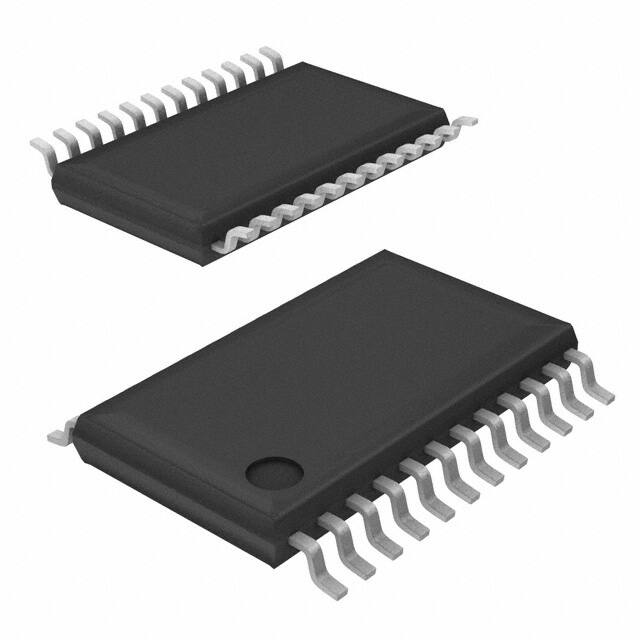


 工商网监
湘ICP备2023018690号
工商网监
湘ICP备2023018690号