MB96300
PRELIMININARY SPECIFICATION
FME-MB96300 rev 19
16-bit Proprietary Microcontroller
CMOS
Y
F2MC-16FX MB96300 Series
AR
■ DESCRIPTION
MB96300 series is based on Fujitsu’s advanced 16FX architecture (16-bit with instruction pipeline for RISC-like
performance). The CPU uses the same instruction set as the established 16LX series - thus allowing for easy
migration of 16LX Software to the new 16FX products. 16FX improvements compared to the previous generation
include significantly improved performance - even at the same operation frequency, reduced power consumption
and faster start-up time.
EL
IM
IN
For highest processing speed at optimized power consumption an internal PLL can be selected to supply the
CPU with up to 56MHz operation frequency from an external 4MHz resonator. The result is a minimum instruction
cycle time of 17.8ns going together with excellent EMI behavior. An on-chip clock modulation circuit significantly
reduces emission peaks in the frequency spectrum. The emitted power is minimised by the on-chip voltage
regulator that reduces the internal CPU voltage. A flexible clock tree allows to select suitable operation frequencies
for peripheral resources independent of the CPU speed.
■ PACKAGES
• 48-pin
PR
48-pin Plastic LQFP
FME/EMDC- 2007-02-12
(FPT-48P-M26)
MB96300_shortspec.fm
�MB96300 Series
Preliminary Specification
• 64-pin
64-pin Plastic LQFP
Y
64-pin Plastic LQFP
(FPT-64P-M24)
AR
(FPT-64P-M23)
• 80-pin
IM
IN
80-pin Plastic LQFP
• 100-pin
PR
EL
(FPT-80P-M21)
100-pin Plastic QFP
100-pin Plastic LQFP
(FPT-100P-M22)
(FPT-100P-M20)
(FPT 100P M05)
2
FME/EMDC- 2007-02-12
MB96300_shortspec.fm
�Preliminary Specification
MB96300
• 120-pin
(FPT 100P M05)
PR
EL
IM
IN
AR
(FPT-120P-M21)
Y
120-pin Plastic LQFP
FME/EMDC- 2007-02-12
MB96300_shortspec.fm
3
�MB96300 Series
Preliminary Specification
■ FEATURES
• 16-bit core CPU, up to 56 MHz internal, 17.8 ns instruction cycle time
• 0.18µm CMOS Process Technology
• Optimized instruction set for controller applications (bit, byte, word and long-word data types; 23 different
addressing modes; barrel shift; variety of pointers)
• 8-byte instruction execution queue
• Signed multiply (16 bit × 16 bit) and divide (32 bit/16 bit) instructions available
Y
• Internal voltage regulator supports reduced internal MCU voltage, offering low EMI and low power
consumption figures
• Code Security Feature
AR
• Up to 5 FULL-CAN interfaces; conforming to Version 2.0 Part A and Part B, ISO16845 certified
• Powerful interrupt functions (8 progr. priority levels; up to 16 external interrupts)
• Fast Interrupt processing
• Up to 16 channels DMA - Automatic transfer function independent of CPU, can be assigned freely to
resources
• Three independent clock timers (23-bit RC clock timer, 23-bit Main clock timer, 17-bit Sub clock timer)
IN
• Watchdog Timer
• Up to 10 channels full duplex USARTs (SCI/LIN)
• Up to 2 channels I2C with 400 kbit/s
• Up to 6 channels16-bit reload timer
IM
• Up to 40 channels analog inputs for A/D Converter (Resolution 10 bits or 8 bits)
• Up to 12 channels ICU (Input capture unit) 16 bit
• Up to 12 channels OCU (Output compare unit) 16 bit
PR
EL
• Up to 4 channels 16-bit free running timer
• Up to 20 channels × 16-bit Programmable Pulse Generator
• Up to 6 channels Stepper Motor Controller with integrated high current output drivers
• LCD controller with up to 4 COM × 72 SEG, internal or external voltage generation
• Memory Patch Function, can also be used to implement embedded debug support
• Low Power Consumption - 13 operating modes : (different Run, Sleep, Timer modes, Stop mode)
• 3-32 MHz external clock, on-chip PLL with programmable multiplication factor 1 ... 16
• 32 kHz Subsystem Clock
• 100kHz/2MHz internal RC clock
• External bus interface with up to 6 Chip select signals, 8bit or 16bit data, 24bit address, multiplexed or nonmultiplexed, programmable timing
• Up to 2 channels Alarm comparators
• Programmable input levels (Automotive / CMOS-Schmitt trigger / TTL) for all ports
• Programmable Pull-up resistors for all ports
• Programmable output driving strength for EMI optimization
• Package : 48-pin / 64-pin / 80-pin /100-pin / 120-pin plastic QFP and LQFP
4
FME/EMDC- 2007-02-12
MB96300_shortspec.fm
�Preliminary Specification
MB96300
PR
EL
IM
IN
AR
Y
• Controller Area Network (CAN) - License of Robert Bosch GmbH
FME/EMDC- 2007-02-12
MB96300_shortspec.fm
5
�MB96300 Series
Preliminary Specification
■ PRODUCT LINEUP
Features
MB96V300
Product type
Evaluation
sample
MB9632x
MB9634x
6kB
288kB
12kB
16kB
416kB
16kB
544kB
24kB
Main:
544kB,
Sat.:
32kB
24kB
Package
Y
160kB
AR
6kB
MB96344R,
MB96344Y
MB96F326R,
MB96F326Y
ROM/Flash
memory
emulation by
external RAM,
92kB internal
RAM
IN
128kB
MB96384R,
MB96384Y
MB96F365R,
MB96F365Y
MB96385R,
MB96385Y
MB96F356R,
MB96F356Y
MB96F346R,
MB96346R,
MB96F346Y,
MB96346Y
MB96F386R,
MB96386R,
MB96F386Y,
MB96386Y
MB96F347R,
MB96347R,
MB96F347Y,
MB96347Y
MB96F387R,
MB96387R,
MB96F387Y,
MB96387Y
IM
RAM
On-chip PLL clock multiplier (x1..16, 1/2 when PLL stop)
Minimum instruction execution time: 17.8 ns (56MHz)
Clock source selectable from main- and subclock oscillator (partnumber suffix “W”), on-chip RC
oscillator, independently for CPU and 2 clock domains of peripherals
PR
EL
Flash/
ROM
Technology
6
MB9638x
F2MC-16FX CPU
System clock
DMA
MB9636x
Flash product: MB96F3xx
Mask ROM product: MB963xx
CPU
288kB
MB9635x
MB96F348R,
MB96F348Y
MB96F348C,
MB96F348H,
MB96F348T
0.18mm CMOS with on-chip voltage regulator for internal power supply
BGA416
FPT-80P-M21
FPT-100PM20
FPT-100PM22
16 channels
4 channels
6 channels
FME/EMDC- 2007-02-12
FPT-64P-M23
FPT-64P-M24
FPT-48P-M26
FPT-120PM21
4 channels
3 channels
7 channels
MB96300_shortspec.fm
�Preliminary Specification
Features
MB96V300
10 channels
MB96300
MB9632x
MB9634x
MB9635x
MB9636x
MB9638x
4 channels
MB96F348H/
T:
4 channels
others:
7 channels
4 channels
2 channels
5 channels
USART
Wide range of baud rate settings using a dedicated reload timer
Special synchronous options for adapting to different synchronous serial protocols
LIN functionality working either as master or slave LIN device
1 channel
2 channel
1 channel
1 channel
Y
2 channels
I2C
Master and Slave functionality, 8-bit and 10-bit addressing
16-bit Reload
Timer
yes
no
6 channels
4 channels
no
4 channels
3 channels
4 channels
4 channels
2 channels
2 channels
1 channel
2 channels
6 channels
8 channels
4 channels
4 channels
Signals an interrupt when a match with 16-bit I/O Timer
A pair of compare registers can be used to generate an output signal.
12 channels
8 channels
6 channels
4 channels
8 channels
PR
Signals an interrupt upon external event
Rising edge, falling edge or rising & falling edge sensitive
20 channels
16-bit
Programmable
Pulse Generator
4 channels
no
Signals an interrupt on overflow, supports timer clear upon match with Output Compare (0, 4), Prescaler
with 1/22, 1/24, 1/26, 1/28 of peripheral clockfrequency
I/O Timer 0 (clock input FRCK0) corresponds to ICU 0/1/2/3, OCU 0/1/2/3
I/O Timer 1 (clock input FRCK1) corresponds to ICU 4/5/6/7, OCU 4/5/6/7
I/O Timer 2 (clock input FRCK2) corresponds to ICU 8/9
I/O Timer 3 (clock input FRCK3) corresponds to ICU 10/11
12 channels
16-bit Input
Capture
yes
MB96384R/Y,
MB96385R/Y:
no
others:
yes
Prescaler with 1/21, 1/22, 1/23, 1/24, 1/25, 1/26 of peripheral clock frequency, event count function
12 channels
16-bit Output
Compare
16 channels
SAR-type, 10bit resolution, signals interrupt on conversion end, single conversion mode, continuous
conversion mode, stop conversion mode, activation by software, external trigger or reload timer
4 channels
16-bit FreeRunning Timer
15 channels
IN
A/D Converter
Reference
Voltage switch
24 channels
EL
IM
A/D Converter
18 channels
AR
40 channels
20 channels
16 channels
20 channels
8 channels
16 bit down counter, cycle and duty setting registers
Interrupt at triggering, cycle or duty match
PWM operation and one-shot operation
Internal prescaler allows 1/2, 1/4, 1/8, 1/16 of peripheral clock as counter clock and Reload timer
overflow as clock input
Can be triggered by software or reload timer
Synchronous trigger of up to 4 PPG channels
FME/EMDC- 2007-02-12
MB96300_shortspec.fm
7
�MB96300 Series
Features
MB96V300
5 channels
MB9632x
MB9634x
2 channels
MB9635x
2 channels
2 channels
MB9636x
MB9638x
1 channel
MB96384R/Y,
MB96385R/Y:
1 channel
others:
2 channels
Supports CAN protocol version 2.0 part A and B
ISO16845 certified
Bit rates up to 1 Mbit/s
32 message objects
Each message object has its own identifier mask
Programmable FIFO mode (concatenation of message objects)
Maskable interrupt
Disabled Automatic Retransmission mode for Time Triggered CAN applications
Programmable loop-back mode for self-test operation
AR
Y
CAN Interface
(not available on
MB963xxA,
MB963xxC)
Preliminary Specification
6 channels
Four high current outputs for each channel
Two synchronized 8/10-bit PWMs per channel
Internal prescaling for PMW clock: 1, 1/2, 1/4, 1/5, 1/6, 1/8, 1/10, 1/12, 1/16 of peripheral clock
16 channels
IM
Non-Maskable
Interrupt
16 channels
13 channels
10 channels
1 channel
Disabled after reset
Once enabled, can not be disabled other than by reset.
Level high or level low sensitive
Pin shared with external interrupt 0.
1channel
Sound Generator
8
2 channels
8-bit PWM signal is mixed with tone frequency from 16-bit reload counter
PWM clock by internal prescaler: 1, 1/2, 1/4, 1/8, 1/16 of peripheral clock
Tone frequency: PWM frequency / 2 / (reload value + 1)
4 COM x 72
SEG
LCD Controller
8 channels
Edge sensitive or level sensitive
Interrupt mask and pending bit per channel
Each available CAN channel RX has an external interrupt for wake-up
Selected USART channels SIN have an external interrupt for wake-up
PR
EL
External
Interrupts
15 channels
IN
Stepping Motor
Controller
5 channels
4 COM x 65
SEG
Display up to 288 segments
Duty cycle: Selectable from options: 1/2, 1/3 and 1/4
Bias: Fixed at 1/3
Frame period: Selectable from three options. (for clock, peripheral clock, subclock or RC oscillator clock
is selectable)
Driver: Built-in (for internal divider resistors), or external divider resistors
Data memory: Built-in 16-byte data memory for display
Stop mode: Enable LCD display in the sub-stop mode
Blank display: Selectable
Pin: All SEG and COM pins can be switched between general and specialized purposes
Others: External divided resistors can be also used to shut off the current when LCD is deactivated
FME/EMDC- 2007-02-12
MB96300_shortspec.fm
�Preliminary Specification
Features
MB96V300
MB9632x
MB96300
MB9634x
MB9635x
MB9636x
MB96F348H/T: no
others: 1
80 for part
number with
suffix "W", 82
for part
number with
suffix "S"
49 for part
number with
suffix "W", 51
for part
number with
suffix "S"
AR
64 for part
number with
suffix "W", 66
for part
number with
suffix "S"
Y
Can be clocked either from sub oscillator (devices with partnumber suffix “W”), main oscillator or from
the RC oscillator
Facility to correct oscillation deviation of Sub clock or RC oscillator clock (clock calibration)
Read/write accessible second/minute/ hour registers
Can signal interrupts every halfsecond/second/ minute/hour/day
Internal clock divider and prescaler provide exact 1s clock based on a 4 MHz or a 32 kHz clock input
(devices with partnumber suffix “W”)
136
I/O Ports
1
34 for part
number with
suffix "W", 36
for part
number with
suffix "S"
94 for part
number with
suffix "W", 96
for part
number with
suffix "S
Virtually all external pins can be used as general purpose I/O
All push-pull outputs (except when used as I2C SDA/SCL line)
Bit-wise programmable input enable
Bit-wise programmable Pull-up resistor
Bit-wise programmable as input/output or peripheral signal
Bit-wise programmable as CMOS schmitt trigger/ automotive / TTL input
Bit-wise programmable output driving strength
IN
Real Time Clock
MB9638x
2 channels
MB96384R/Y,
MB96385R/Y:
1 channel
others:
2 channels
EL
IM
2 channels
Alarm comparator
Monitors an external voltage and generates an interrupt in case of a voltage lower or higher than the
defined thresholds
Threshold voltages defined externally or generated internally
Status is readable, interrupts can be masked separately
Yes
Chip select
Clock output
function
Multiplexed address/data lines
Non-multiplexed address/data lines (MB96V300 and MB9638x only)
16-bit bidirectional data bus
24-bit address lines (MB9635x: 22-bit address lines)
Wait state request
External bus master possible
Timing programmable
PR
External bus
interface
Yes
6 signals
6 signals
6 signals
6 signals
2 channels
2 channels
2 channels
2 channels
6 signals
2 channels
2 channels
Output any on-chip clock
Inverted and non-inverted clock (MB9636x,MB9635x has only non-inverted clock output)
Prescaler: 1, 1/2, 1/4, 1/8, 1/16, 1/32, 1/64, 1/128 of selected clock
Synchronous or asynchronous start/stop
Low voltage reset
FME/EMDC- 2007-02-12
Reset is generated when supply voltage is below minimum.
MB96300_shortspec.fm
9
�MB96300 Series
On-chip RCoscillator
MB96V300
MB9632x
MB9634x
MB9636x
MB9638x
For quick and save startup, oscillator stop detection, watchdog operation, normal clock source
2 frequencies selectable (100kHz, 2MHz)
Supports automatic programming, Embedded AlgorithmTM*1
Write/Erase/Erase-Suspend/Resume commands
A flag indicating completion of the algorithm
Number of erase cycles : 10,000 times
Data retention time : 20 years
Erase can be performed on each sector individually
Sector protection
Flash Security feature to protect the content of the Flash
Low voltage detection during Flash erase
Flash Memory
: Embedded Algorithm is a trade mark of Advanced Micro Devices Inc.
PR
EL
IM
IN
AR
*1
MB9635x
Y
Features
Preliminary Specification
10
FME/EMDC- 2007-02-12
MB96300_shortspec.fm
�Preliminary Specification
MB96300
■ PIN ASSIGNMENTS
61
62
P17_2 /FRCK3/TTG17
63
P13_5 /PPG17
64
P02_5 /A21/IN1/TTG1/TTG9/ADTG_R
65
P04_4 /SDA0/FRCK0/TIN0_R
66
P04_5 /SCL0/FRCK1/TIN2_R
67
P03_0 /ALE/IN4/TTG4/TTG12/TOT0_R
68
Y
P01_1/AD09/TOT1/CKOTX1/TTG17_R
P01_2/AD10/SIN3/INT11_R/TTG18_R
P01_3/AD11/SOT3/TTG19_R
P01_4/AD12/SCK3/PPG16_R
P01_5/AD13/SIN2_R/INT7_R/PPG17_R
P01_6/AD14/SOT2_R/PPG18_R
P01_7/AD15/SCK2_R/PPG19_R
P09_2/PPG10/CS5
P09_3/PPG11/CS4/FRCK2_R
P02_0/A16/PPG12/CKOT1_R
P02_1/A17/PPG13
P02_2/A18/PPG14/CKOT0_R
P02_3/A19/PPG15
P02_4/A20/IN0/TTG0/TTG8
RSTX
P02_6/A22/IN2/TTG2/ TTG10
P02_7 /A23/IN3/TTG3/ TTG11
X1
AR
C
60 59 58 57 56 55 54 53 52 51 50 49 48 47 46 45 44 43 42 41
LQFP-80
IN
Vcc
X0
Vss
Pin assignment of MB96(F)32x
40
P01_0/AD08/TIN1/CKOT1/TTG16_R
39
P09_1 /PPG9/LBX
38
P09_0 /PPG8/UBX
37
36
P00_7 /AD07/INT15/PPG11_R
P00_6 /AD06/INT14/PPG10_R
35
P00_5/AD05/NT13/SIN8_R/PPG9_R
34
P00_4/AD04/INT12/SOT8_R/PPG8_R
33
P00_3/AD03/INT11/SCK8_R/TTG11_R
32
P00_2/AD02/INT10/SIN7_R/TTG10_R
31
P00_1 /AD01/INT9/SOT7_R/TTG9_R
30
P00_0/AD00/INT8/SCK7_R/TTG8_R
29
P17_7/TX3/IN11/TTG19
28
MD_0
27
MD_1
P03_1 /RDX/IN5/TTG5 /TTG13/TOT2_R
69
P03_2 /WRLX/INT10_R /RX2
70
P03_3 /WRHX /TX2
71
P03_4 /HRQ/OUT4
72
P03_5 /HAKX/OUT5
73
P03_6 /RDY/OUT6
74
P03_7/CLK /OUT7
75
26
MD_2
P13_6 /PPG18/IN8
P13_7 /PPG19/IN9
76
25
X1A*/P04_1*
77
24
X0A*/P04_0*
P06_0 /AN0/PPG0/CS0_R
78
23
Vss
P06_1/AN /PPG1/CS1_R
79
22
Vcc
AVcc
80
21
P04_3/IN7/TX1/TTG7/TTG15
Package code(mold)
P17_6/OUT11/IN10/TTG18/INT3_R
P04_2/IN6/RX1/INT9_R/TTG6/TTG14
P07_0/AN16/INT0/NMI
P05_7/AN15/INT5_R/OUT10_R
P05_6/AN14/INT4_R
P06_5/AN5/PPG5/CS5_R
P05_5/AN13/ INT0_R/NMI_R
P06_4/AN4/PPG4/CS4_R
P05_4/AN12/TOT3/INT2_R
P06_3/AN3/PPG3/CS3_R
P05_3/AN11/TIN3/WOT
P06_2 /AN2/PPG2/CS2_R
9 10 11 12 13 14 15 16 17 18 19 20
P05_2/AN10/SCK2
AVss
7 8
P05_1/AN9/SOT2
6
P05_0/AN8/SIN2 /INT3_R1
5
P07_1/AN17/INT1
4
P06_7/AN7/PPG7
3
P06_6/AN6/PPG6
2
PR
1
AVRH
EL
IM
FPT-80P-M21
1) Devices with suffix W: X0A/X1A
Devices with suffix S: P04_0, P04_1
FME/EMDC- 2007-02-12
(FPT-80P-M21)
MB96300_shortspec.fm
11
�MB96300 Series
Preliminary Specification
MD2
MD1
MD0
RSTX
P07_6/AN22/INT6/SOT9_R2)
P07_7/AN23/INT7/SIN9_R2)
P08_0/TIN0/CKOTX0/ADTG/INT12_R
P08_1/TOT0/CKOT0/INT13_R
P08_2/SIN0/TIN2/INT14_R
P08_3/SOT0/TOT2
P08_4/SCK0/INT15_R
P08_5/SIN1/INT1_R
P08_6/SOT1
P08_7/SCK1
Vcc
Vss
P09_0/PPG8/UBX
P09_1/PPG9/LBX
P09_2/PPG10/CS5
P09_3/PPG11/CS4
P09_4/OUT0/CS3
P09_5/OUT1/CS2
P09_6/OUT2/CS1
P09_7/OUT3/CS0
P10_0/RX0/INT8_R
P10_1/TX0
P00_0/AD00/INT8/SCK7_R2)
P00_1/AD01/INT9/SOT7_R2)
P00_2/AD02/INT10/SIN7_R2)
P00_3/AD03/INT11/SCK8_R2)
Pin assignment of MB96(F)34x (QFP package)
Y
80 79 78 77 76 75 74 73 72 71 70 69 68 67 66 65 64 63 62 61 60 59 58 57 56 55 54 53 52 51
81
P00_5/AD05/INT13/SIN8_R2)
82
P00_6/AD06/INT14
83
P00_7/AD07/INT15
84
P01_0/AD08/CKOT1/TIN1
85
P01_1/AD09/CKOTX1/TOT1
86
P01_2/AD10/INT11_R/SIN3
87
P01_3/AD11/SOT3
88
P01_4/AD12/SCK3
89
Vcc
90
Vss
91
X1
92
X0
93
P01_5/AD13/INT7_R/SIN2_R
94
P01_6/AD14/SOT2_R
95
P01_7/AD15/SCK2_R
96
P02_0/A16/PPG12
97
P02_1/A17/PPG13
98
P02_2/A18/PPG14
99
P02_3/A19/PPG15
100
QFP - 100
IN
P07_5/AN21/INT5/SCK9_R2)
49
P07_4/AN20/INT4
48
P07_3/AN19/INT3
47
P07_2/AN18/INT2
46
P07_1/AN17/INT1
45
P07_0/AN16/INT0/NMI
44
Vss
43
P06_7/AN7/PPG7
42
P06_6/AN6/PPG6
41
P06_5/AN5/PPG5
40
P06_4/AN4/PPG4
39
P06_3/AN3/PPG3
38
P06_2/AN2/PPG2
37
P06_1/AN1/PPG1
36
P06_0/AN0/PPG0
35
AVss
34
AVRL
33
AVRH
32
31
AVcc
P05_7/AN15/INT5_R
P05_6/AN14/INT4_R
P05_5/AN13/INT0_R/NMI_R
P05_4/AN12/TOT3/INT2_R
P05_3/AN11/TIN3/WOT
P05_2/AN10/SCK2
P05_1/AN9/ALARM1/SOT2
P05_0/AN8/ALARM0/SIN2/INT3_R1
P04_7/SCL1
P04_6/SDA1
P04_5/SCL0/FRCK1
P04_4/SDA0/FRCK0
P04_3/IN7/TX1/TTG7/TTG15
P04_2/IN6/RX1/INT9_R/TTG6/TTG14
C
Vss
Vcc
X1A /P04_1
1)
1)
P03_1/RDX/IN5/TTG5/TTG13
X0A /P04_0
P03_0/ALE/IN4/TTG4/TTG12
1)
P02_7/A23/IN3/TTG3/TTG11
50
9 10 11 12 13 14 15 16 17 18 19 20 21 22 23 24 25 26 27 28 29 30
1)
P02_6/A22/IN2/TTG2/TTG10
8
P03_7/CLK/OUT7
P02_4/A20/TTG8/TTG0/IN0
7
IM
6
P03_6/RDY/OUT6
5
P03_5/HAKX/OUT5
4
P03_4/HRQ/OUT4
3
P03_3/WRHX
2
P03_2/WRLX/WRX/INT10_R
1
P02_5/A21/TTG9/TTG1/IN1/ADTG_R
Package code (mold)
FPT-100P-M22
PR
EL
1)
AR
P00_4/AD04/INT12/SOT8_R2)
Devices with suffix W: X0A/X1A
Devices with suffix S: P04_0, P04_1
2) SIN7_R, SOT7_R, SCK7_R, SIN8_R, SOT8_R, SCK8_R, SIN9_R, SOT9_R, SCK9_R only available on MB96F348R/Y
(FPT-100P-M22)
Remark:
MB96(F)34x products are pin-compatible to F2MC-16LX family MB90340 series.
12
FME/EMDC- 2007-02-12
MB96300_shortspec.fm
�Preliminary Specification
MB96300
84
P01_2/AD10/INT11_R/SIN3
85
P01_3/AD11/SOT3
86
P01_4/AD12/SCK3
87
Vcc
88
Vss
89
X1
90
X0
91
P01_5/AD13/INT7_R/SIN2_R
92
P01_6/AD14/SOT2_R
93
P01_7/AD15/SCK2_R
94
P02_0/A16/PPG12
95
P02_1/A17/PPG13
96
P02_2/A18/PPG14
97
P02_3/A19/PPG15
98
P02_4/A20/TTG8/TTG0/IN0
99
1)
MD0
RSTX
P07_6/AN22/INT6/AIN2/SOT9_R2)
P07_7/AN23/INT7/AIN3/SIN9_R2)
P08_0/TIN0/CKOTX0/ADTG/INT12_R
P08_1/TOT0/CKOT0/INT13_R
P08_2/SIN0/TIN2/INT14_R
P08_3/SOT0/TOT2
P08_4/SCK0/INT15_R
P08_5/SIN1/INT1_R
P08_6/SOT1
P08_7/SCK1
Vcc
Vss
P09_0/PPG8/UBX
P09_1/PPG9/LBX
P09_2/PPG10/CS5
P09_3/PPG11/CS4
P09_4/OUT0/CS3
P09_5/OUT1/CS2
P09_6/OUT2/CS1
P09_7/OUT3/CS0
P10_0/RX0/INT8_R
LQFP - 100
Package code (mold)
FPT-100P-M20
P03_0/ALE/IN4/TTG4/TTG12
P03_1/RDX/IN5/TTG5/TTG13
P03_2/WRLX/WRX/INT10_R
P03_3/WRHX
P03_4/HRQ/OUT4
Vss
7 8
Vcc
6
X1A1)/P04_11)
5
X0A1)/P04_01)
4
P03_7/CLK/OUT7
3
MD2
48
P07_5/AN21/INT5/SCK9_R2)
47
P07_4/AN20/INT4
46
P07_3/AN19/INT3
45
P07_2/AN18/INT2
44
P07_1/AN17/INT1
43
P07_0/AN16/INT0/NMI
42
Vss
41
P06_7/AN7/PPG7
40
P06_6/AN6/PPG6
39
P06_5/AN5/PPG5
38
P06_4/AN4/PPG4
37
P06_3/AN3/PPG3
36
P06_2/AN2/PPG2
35
P06_1/AN1/PPG1
34
P06_0/AN0/PPG0
33
AVss
32
AVRL
31
AVRH
30
AVcc
29
P05_7/AN15/INT5_R
28
P05_6/AN14/INT4_R
27
P05_5/AN13/INT0_R/NMI_R
26
9 10 11 12 13 14 15 16 17 18 19 20 21 22 23 24 25
P03_6/RDY/OUT6
2
P03_5/HAKX/OUT5
1
P02_7/A23/IN3/TTG3/TTG11
100
P02_6/A22/IN2/TTG2/TTG10
P02_5/A21/TTG9/TTG1/IN1/ADTG_R
Y
P01_1/AD09/CKOTX1/TOT1
MD1
P05_4/AN12/TOT3/INT2_R
P05_3/AN11/TIN3/WOT
83
P05_2/AN10/SCK2
P01_0/AD08/CKOT1/TIN1
P05_1/AN9/ALARM1/SOT2
82
P05_0/AN8/ALARM0/SIN2/INT3_R1
P00_7/AD07/INT15
P04_7/SCL1
81
AR
80
P00_6/AD06/INT14
P04_6/SDA1
P00_5/AD05/INT13/SIN8_R2)
P04_5/SCL0/FRCK1
79
P04_4/SDA0/FRCK0
P00_4/AD04/INT12/SOT8_R2)
P04_3/IN7/TX1/TTG7/TTG15
78
49
IN
P00_3/AD03/INT11/SCK8_R2)
75 74 73 72 71 70 69 68 67 66 65 64 63 62 61 60 59 58 57 56 55 54 53 52 51
50
P04_2/IN6/RX1/INT9_R/TTG6/TTG14
77
C
76
EL
IM
P00_1AD01/INT9/SOT7_R2)
P00_2/AD02/INT10/SIN7_R2)
P10_1/TX0
P00_0/AD00/INT8/SCK7_R2)
Pin assignment of MB96(F)34x (LQFP package)
PR
Devices with suffix W: X0A/X1A
Devices with suffix S: P04_0, P04_1
2) SIN7_R, SOT7_R, SCK7_R, SIN8_R, SOT8_R, SCK8_R, SIN9_R, SOT9_R, SCK9_R only available on MB96F348R/Y
(FPT-100P-M20)
Remark:
MB96(F)34x products are pin-compatible to F2MC-16LX family MB90340 series.
FME/EMDC- 2007-02-12
MB96300_shortspec.fm
13
�MB96300 Series
Preliminary Specification
Y
P01_1/AD09/CKOTX1/TOT1/TTG17_R
P01_2/AD10/INT11_R/SIN3/TTG18_R
P01_3/AD11/SOT3/TTG19_R
P01_4/AD12/SCK3/PPG16_R
P01_5/AD13/SIN2_R/INT7_R/PPG17_R
P01_6/AD14/SOT2_R/PPG18_R
P01_7/AD15/SCK2_R/PPG19_R
P02_0/A16/PPG12/CKOT1_R
P02_1/A17/PPG13
P02_2/A18/PPG14/CKOT0_R
P02_3/A19/PPG15
P02_4/A20/TTG8/TTG0/IN0
RSTX
X1
X0
Vss
Pin assignment of MB96(F)35x
48 47 46 45 44 43 42 41 40 39 38 37 36 35 34 33
49
32
P01_0/AD08/CKOT1/TIN1/TTG16_R
C
50
P00_7/AD07/INT15/PPG11_R
P02_5/A21/TTG9/TTG1/IN1/ADTG_R
51
P04_4/SDA0/FRCK0/TIN0_R
52
P04_5/SCL0/FRCK1/TIN2_R
53
P03_0/ALE/IN4/TTG4/TTG12/TOT0_R
54
P03_1/RDX/IN5/TTG5/TTG13/TOT2_R
55
P03_2/WRLX/WRX/RX2/INT10_R
56
P03_3/TX2/WRHX
57
P03_4/HRQ/OUT4
58
P03_5/HAKX/OUT5
59
P03_6/RDY/OUT6
60
P03_7/CLK/OUT7
61
P06_0/AN0/PPG0/CS0_R
62
P06_1/AN1/PPG1/CS1_R
63
AVcc
64
AR
31
LQFP - 64
IN
P00_6/AD06/INT14/PPG10_R
29
P00_5/AD05/INT13/SIN8_R/PPG9_R
28
P00_4/AD04/INT12/SOT8_R/PPG8_R
27
P00_3/AD03/INT11/SCK8_R/TTG11_R
26
P00_2/AD02/INT10/SIN7_R/TTG10_R
25
P00_1/AD01/INT9/SOT7_R/TTG9_R
24
P00_0/AD00/INT8/SCK7_R/TTG8_R
23
MD0
22
MD1
21
MD2
20
X1A*/P04_1*
19
X0A*/P04_0*
18
Vss
P05_6/AN14/INT4_R
P05_5/AN13/INT0_R/NMI_R
P05_4/AN12/TOT3/INT2_R
P05_3/AN11/TIN3/WOT
P04_3/IN7/TX1/TTG7/TTG15
P04_2/IN6/RX1/INT9_R/TTG6/TTG14
PR
EL
P05_2/AN10/SCK2
8
P05_1/AN9/SOT2
7
30
17
9 10 11 12 13 14 15 16
P05_0/AN8/SIN2/INT3_R1
P06_3/AN3/PPG3/CS3_R
6
P06_7/AN7/PPG7
P06_2/AN2/PPG2/CS2_R
5
P06_6/AN6/PPG6
4
P06_5/AN5/PPG5/CS5_R
3
IM
2
P06_4/AN4/PPG4/CS4_R
1
AVss
Package code (mold)
FPT-64P-M23/M24
AVRH
Vcc
1) Devices with suffix W: X0A/X1A
Devices with suffix S: P04_0, P04_1
(FPT-64P-M23/M24)
Remark:
MB96(F)35x products are pin-compatible to F2MC-16LX family MB90350 series.
14
FME/EMDC- 2007-02-12
MB96300_shortspec.fm
�Preliminary Specification
MB96300
C
Vss
X0
X1
P02_7/IN3/TTG3/TTG11
P02_6/IN2/TTG2/TTG10
P02_5/TTG9/TTG1/IN1/ADTG_R
P02_4/TTG8/TTG0/IN0
P02_3/PPG15
P02_2/PPG14/CKOT0_R
P02_1/PPG13
P02_0/PPG12/CKOT1_R
Pin assignment of MB96(F)36x
36 35 34 33 32 31 30 29 28 27 26 25
37
24
Vcc
P08_7/SCK1
38
23
RSTX
P08_6/SOT1
39
22
P04_3/TX1/TTG7/TTG15
40
P04_2/RX1/INT9_R/TTG6/TTG14
41
P08_3/SOT0/TOT2
42
P08_4/SCK0/INT15_R
43
P08_2/SIN0/TIN2/INT14_R
44
P04_4/FRCK0
45
X0A*/P04_0*
46
X1A*/P04_1*
47
AVss
48
LQFP-48
21
20
19
MD0
MD1
MD2
P05_7/AN15/INT5_R
P05_6/AN14/INT4_R
AR
18
Y
P08_5/SIN1/INT1_R
6
7
8
AVcc
P06_0/AN0
P06_1/AN1
P06_2/AN2
P06_3/AN3
P06_4/AN4/PPG4
P06_5/AN5/PPG5
P05_4/AN12/TOT3/INT2_R
15
P05_3/AN11/TIN3
14
P05_2/AN10
P05_1/AN9
P05_0/AN8/SIN2/INT3_R1
5
P08_0/ADTG/CKOTX0/INT12_R
4
P06_7/AN7/PPG7
3
P05_5/AN13/INT0_R/NMI_R
16
EL
IM
IN
2
17
13
9 10 11 12
P06_6/AN6/PPG6
1
AVRH
Package code (mold)
FPT-48P-M26
* Devices with suffix W: X0A/X1A
Devices with suffix S: P04_0, P04_1
PR
(FPT-48P-M26)
Remark:
MB96(F)36x products are pin-compatible to F2MC-16LX family MB90360 series
FME/EMDC- 2007-02-12
MB96300_shortspec.fm
15
�MB96300 Series
Preliminary Specification
Vcc
P00_2/INT5_R/RDY/SEG14
P00_1/INT4_R/WRHX/SEG13
P00_0/INT3_R/HAKX/SEG12
P12_7/INT1_R/HRQ/SEG11
P12_6/TOT2_R/A15/SEG10
P12_5/TIN2_R/A14/SEG9
P12_4/OUT3_R/A13/SEG8
P12_3/OUT2_R/A12/SEG7
P12_2/TOT1_R/A11/SEG6
P12_1/TIN1_R/A10/SEG5
P12_0/IN1_R/A09/SEG4
P11_7/IN0_R/A08/SEG3
P11_6/FRCK0_R/A07/SEG2
P11_5/PPG4_R/A06/SEG1
P11_4/PPG3_R/A05/SEG0
P11_3/PPG2_R/A04/COM3
P11_2/PPG1_R/A03/COM2
P11_1/PPG0_R/A02/COM1
P11_0/A01/COM0/CS5
RSTX
X1A/P04_1 1)
X0A/P04_0 1)
Vss
X1
X0
MD2
MD1
MD0
Vss
Pin assignment of MB96(F)38x
90 89 88 87 86 85 84 83 82 81 80 79 78 77 76 75 74 73 72 71 70 69 68 67 66 65 64 63 62 61
60
92
59
Y
91
93
94
AR
95
96
97
98
99
100
101
102
LQFP - 120
103
104
105
IN
106
Package code (mold)
FPT-120P-M21
107
108
109
110
111
112
113
114
115
116
117
118
119
120
2
3
4
5
6
7
8
58
57
56
55
54
53
52
51
50
49
48
47
46
45
44
43
42
41
40
39
38
37
36
35
34
33
32
31
9 10 11 12 13 14 15 16 17 18 19 20 21 22 23 24 25 26 27 28 29 30
Vcc
P10_3/PWM2M4/PPG7
P10_2/PWM2P4/SCK2/PPG6
P10_1/PWM1M4/SOT2/TOT3
P10_0/PWM1P4/SIN2/TIN3
P09_7/PWM2M3
DVss
DVcc
P09_6/PWM2P3
P09_5/PWM1M3
P09_4/PWM1P3
P09_3/PWM2M2
P09_2/PWM2P2
P09_1/PWM1M2
P09_0/PWM1P2
P08_7/PWM2M1
P08_6/PWM2P1
P08_5/PWM1M1
DVss
DVcc
P08_4/PWM1P1
P08_3/PWM2M0
P08_2/PWM2P0
P08_1/PWM1M0
P08_0/PWM1P0
P05_7/AN15/TOT2/SGA1_R/SEG64
P05_6/AN14/TIN2/SGO1_R/SEG63
P05_5/AN13/TX1/SEG62 3)
P05_4/AN12/RX1/INT2_R/SEG61 3)
Vss
Vss
C
P03_7/INT1/SIN1/CS0/A20/SEG40
P13_0/INT2/SOT1/CS1/A21/SEG41
P13_1/INT3/SCK1/CS2/A22/SEG42
P13_2/PPG0/TIN0/FRCK1/CS3/A23/SEG43
P13_3/PPG1/TOT0/WOT/UBX/SEG44
P13_4/SIN0/INT6/SEG45
P13_5/SOT0/ADTG/INT7/SEG46
P13_6/SCK0/CKOTX0/LBX/SEG47
P13_7/PPG2/CKOT0/CS4/SEG48
P04_4/PPG3/SDA0
P04_5/PPG4/SCL0
P06_0/AN0/SCK5/IN2_R/SEG49
P06_1/AN1/SOT5/IN3_R/SEG50
P06_2/AN2/INT5/SIN5/SEG51
P06_3/AN3/FRCK0/SEG52
P06_4/AN4/IN0/TTG0/TTG4/SEG53
P06_5/AN5/IN1/TTG1/TTG5/SEG54
P06_6/AN6/TIN1/IN4_R/SEG55
P06_7/AN7/TOT1//IN5_R/SEG56
AVcc
AVRH
AVRL/AVRH2
AVss
P05_0/AN8/ALARM0/SEG57
2) P05_1/AN9/ALARM1/SEG58
P05_2/AN10/OUT2/SGO1/SEG59
P05_3/AN11/OUT3/SGA1/SEG60
Vcc
PR
EL
1
IM
Vss
P00_3/INT6_R/A00/CS3_R/SEG15
P00_4/INT7_R/ALE/SEG16
P00_5/TTG2/IN6/RDX/SEG17
P00_6/TTG3/IN7/WRLX/WRX/SEG18
P00_7/SGO0/CLK/SEG19
P01_0/SGA0/AD00/SEG20
P01_1/OUT0/CKOT1/AD01/SEG21
P01_2/OUT1/CKOTX1/AD02/SEG22
P01_3/PPG5/AD03/SEG23
P01_4/AD04/SIN4/SEG24
P01_5/AD05/SOT4/SEG25
P01_6/AD06/SCK4/SEG26
P01_7/CKOTX1_R/AD07/SEG27
P02_0/CKOT1_R/AD08/SEG28
P02_1/IN6_R/AD09/SEG29
P02_2/IN7_R/AD10/SEG30
P02_3/SGO0_R/AD11/SEG31
P02_4/SGA0_R/AD12/SEG32
P02_5/OUT0_R/AD13/SEG33
P02_6/OUT1_R/AD14/SEG34
P02_7/PPG5_R/AD15/SEG35
P03_0/V0/A16/SEG36
P03_1/V1/A17/SEG37
P03_2/V2/A18/SEG38
P03_3/V3/A19/SEG39
P03_4/INT4/RX0
P03_5/TX0
P03_6/NMI/INT0
Vcc
1) Devices with suffix W: X0A/X1A
Devices with suffix S: P04_0, P04_1
2) MB96384/5: Alarm1 not available
3) MB96384/5: TX1 resp. RX1 not available
(FPT-120P-M21)
16
FME/EMDC- 2007-02-12
MB96300_shortspec.fm
�Preliminary Specification
MB96300
■ PIN DESCRIPTION FOR MB96(F)32x, MB96(F)34x, MB96(F)35x, MB96(F)36x
PIN DESCRIPTION FOR MB96(F)32x, MB96(F)34x, MB96(F)35x, MB96(F)36x
Pin no.
MB9632
x
MB9634x
MB9635
x
MB9636
x
LQFP80*5
LQFP100*2
QFP100*1
LQFP64*3
LQFP48*4
58
90
92
46
28
Pin name
Circuit
type
X1
Function
Oscillation output
91
93
47
27
X0
55
52
54
45
23
RSTX
77
76
78
FME/EMDC- 2007-02-12
Reset input
General purpose I/O
AD00
External bus interface (nonmultiplexed mode) data line
External bus interface
(multiplexed mode) address/
data line
H
INT8
External interrupt request
input pin for INT8
SCK7_R
Relocated USART7 serial
clock I/O (not available on
MB96F348H/T)
TTG8_R
Relocated PPG8 trigger
P00_1
General purpose I/O
AD01
External bus interface (nonmultiplexed mode) data line
External bus interface
(multiplexed mode) address/
data line
25
PR
31
EL
IM
24
E
P00_0
IN
75
30
Oscillation input
AR
59
Y
A
H
INT9
SOT7_R
TTG9_R
External interrupt request
input pin for INT9
Relocated USART 7 serial
data output (not available on
MB96F348H/T)
Relocated PPG9 trigger
MB96300_shortspec.fm
17
�MB96300 Series
Preliminary Specification
PIN DESCRIPTION FOR MB96(F)32x, MB96(F)34x, MB96(F)35x, MB96(F)36x
Pin no.
LQFP100*2
77
QFP100*1
MB9635
x
MB9636
x
LQFP64*3
LQFP48*4
79
32
Pin name
Circuit
type
26
P00_2
General purpose I/O
AD02
External bus interface (nonmultiplexed mode) data line
External bus interface
(multiplexed mode) address/
data line
H
INT10
IN
SIN7_R
78
80
IM
TTG10_R
18
FME/EMDC- 2007-02-12
External interrupt request
input pin for INT10
Relocated USART 7 serial
data input (not available on
MB96F348H/T)
Relocated PPG10 trigger
P00_3
General purpose I/O
AD03
External bus interface (nonmultiplexed mode) data line
External bus interface
(multiplexed mode) address/
data line
27
PR
EL
33
Function
Y
LQFP80*5
MB9634x
AR
MB9632
x
H
INT11
External interrupt request
input pin for INT11
SCK8_R
Relocated USART8 serial
clock I/O (not available on
MB96F348H/T)
TTG11_R
Relocated PPG11 trigger
MB96300_shortspec.fm
�Preliminary Specification
MB96300
PIN DESCRIPTION FOR MB96(F)32x, MB96(F)34x, MB96(F)35x, MB96(F)36x
Pin no.
LQFP100*2
QFP100*1
79
MB9635
x
MB9636
x
LQFP64*3
LQFP48*4
81
34
28
Pin name
Circuit
type
P00_4
General purpose I/O
AD04
External bus interface (nonmultiplexed mode) data line
External bus interface
(multiplexed mode) address/
data line
INT12
H
SOT8_R
29
PR
35
FME/EMDC- 2007-02-12
External interrupt request
input pin for INT12
Relocated USART 8 serial
data output (not available on
MB96F348H/T)
PPG8_R
Relocated
Programmable Pulse
Generator outputs
P00_5
General purpose I/O
AD05
External bus interface (nonmultiplexed mode) data line
External bus interface
(multiplexed mode) address/
data line
IN
82
EL
IM
80
Function
Y
LQFP80*5
MB9634x
AR
MB9632
x
INT13
SCK8_R
PPG9_R
H
External interrupt request
input pin for INT13
Relocated USART8 serial
clock I/O (not available on
MB96F348H/T)
Relocated
Programmable Pulse
Generator outputs
MB96300_shortspec.fm
19
�MB96300 Series
Preliminary Specification
PIN DESCRIPTION FOR MB96(F)32x, MB96(F)34x, MB96(F)35x, MB96(F)36x
Pin no.
MB9632
x
LQFP80*5
MB9634x
LQFP100*2
QFP100*1
MB9635
x
MB9636
x
LQFP64*3
LQFP48*4
Pin name
Circuit
type
P00_6 to
P00_7
Y
AD06 to
AD07
83 to 84
36 to 37
General purpose I/O
AR
81 to 82
30 to 31
H
INT14 to
INT15
84
41
20
P01_0
General purpose I/O
AD08
External bus interface (nonmultiplexed mode) data line
External bus interface
(multiplexed mode) address/
data line
H
Reload Timer 1 event input
pin
TIN1
CKOT1
Clock Output Function 1
clock output
TTG16_R
Relocated PPG16 trigger
input
P01_1
General purpose I/O
AD09
External bus interface (nonmultiplexed mode) data line
External bus interface
(multiplexed mode) address/
data line
86
FME/EMDC- 2007-02-12
External interrupt request
input pins for INT14 to INT15
Relocated
Programmable Pulse
Generator outputs
32
PR
EL
40
External bus interface (nonmultiplexed mode) data lines
External bus interface
(multiplexed mode) address/
data lines
PPG10_R
to
PPG11_R
IN
85
IM
83
Function
33
H
TOT1
Reload Timer 1 output
CKOTX1
Clock Output Function 1
inverted Clock Output
TTG17_R
Relocated PPG17 trigger
MB96300_shortspec.fm
�Preliminary Specification
MB96300
PIN DESCRIPTION FOR MB96(F)32x, MB96(F)34x, MB96(F)35x, MB96(F)36x
Pin no.
LQFP100*2
QFP100*1
85
MB9635
x
MB9636
x
LQFP64*3
LQFP48*4
Pin name
34
General purpose I/O
AD10
External bus interface (nonmultiplexed mode) data line
External bus interface
(multiplexed mode) address/
data line
H
SIN3
INT11_R
TTG18_R
88
87
89
EL
IM
35
PR
FME/EMDC- 2007-02-12
Relocated external interrupt
request input for INT11
Relocated PPG18 trigger
General purpose I/O
AD11
External bus interface (nonmultiplexed mode) data line
External bus interface
(multiplexed mode) address/
data line
H
SOT3
USART 3 serial data output
TTG19_R
Relocated PPG19 trigger
P01_4
General purpose IO
AD12
External bus interface (nonmultiplexed mode) data line
External bus interface
(multiplexed mode) address/
data line
36
44
USART 3 serial data input
P01_3
IN
86
43
Function
P01_2
87
42
Circuit
type
Y
LQFP80*5
MB9634x
AR
MB9632
x
H
SCK3
USART 3 clock I/O
PPG16_R
Relocated Pulse
Programable output
MB96300_shortspec.fm
21
�MB96300 Series
Preliminary Specification
PIN DESCRIPTION FOR MB96(F)32x, MB96(F)34x, MB96(F)35x, MB96(F)36x
Pin no.
LQFP100*2
92
QFP100*1
MB9635
x
MB9636
x
LQFP64*3
LQFP48*4
94
Circuit
type
37
General purpose IO
AD13
External bus interface (nonmultiplexed mode) data line
External bus interface
(multiplexed mode) address/
data line
H
95
INT7_R
Relocated external interrupt
request pin for INT7
SIN2_R
Relocated USART 2 serial
data input
PPG17_R
Relocated Pulse
Programable output
P01_6
General purpose IO
AD14
External bus interface (nonmultiplexed mode) data line
External bus interface
(multiplexed mode) address/
data line
38
PR
EL
46
94
47
22
IM
93
96
FME/EMDC- 2007-02-12
Function
P01_5
IN
45
Pin name
Y
LQFP80*5
MB9634x
AR
MB9632
x
H
Relocated USART2 serial
data output
SOT2_R
PPG18_R
Relocated Pulse
Programable output
P01_7
General purpose IO
AD15
External bus interface (nonmultiplexed mode) data line
External bus interface
(multiplexed mode) address/
data line
39
H
SCK2_R
PPG19_R
Relocated USART2 clock I/O
Relocated Pulse
Programable output
MB96300_shortspec.fm
�Preliminary Specification
MB96300
PIN DESCRIPTION FOR MB96(F)32x, MB96(F)34x, MB96(F)35x, MB96(F)36x
Pin no.
MB9632
x
LQFP80*5
MB9634x
LQFP100*2
QFP100*1
MB9635
x
MB9636
x
LQFP64*3
LQFP48*4
Pin name
Circuit
type
P02_0
General purpose IO
PPG12
Programmable Pulse
Generator outputs
97
50
40
Y
36
95
H
AR
A16
36
CKOT1_R
P02_1
35
96
98
H
PPG13
41
IN
51
EL
IM
52
54
98
99
100
43
PR
53
1
44
33
Programmable Pulse
Generator output
PPG14
Programmable Pulse
Generator output
H
External bus interface
address output
A18
CKOT0_R
Relocated Clock Output
Function 0 clock output
P02_3
PPG15
General purpose IO
H
P02_4
General purpose IO
32
Input Capture Unit 0 data
sample input
IN0
TTG0/
TTG8
Programmable Pulse
Generator output
External bus interface
address output
A19
A20
FME/EMDC- 2007-02-12
General purpose IO
General purpose IO
42
34
Relocated Clock Output
Function 1 clock output
P02_2
34
99
External bus interface
address output
External bus interface
address output
A17
97
Function
H
Programmable Pulse
Generator PPG0 and PPG8
trigger input
External bus interface
address output
MB96300_shortspec.fm
23
�MB96300 Series
Preliminary Specification
PIN DESCRIPTION FOR MB96(F)32x, MB96(F)34x, MB96(F)35x, MB96(F)36x
Pin no.
MB9632
x
LQFP80*5
MB9634x
LQFP100*2
QFP100*1
MB9635
x
MB9636
x
LQFP64*3
LQFP48*4
Pin name
Circuit
type
P02_5
1
51
H
AR
100
Relocated A/D converter
trigger input
Y
IN1
65
General purpose IO
ADTG_R
31
TTG1/
TTG9
A21
3
68
3, 4
5
54
FME/EMDC- 2007-02-12
Programmable Pulse
Generator PPG1 and PPG9
trigger
External bus interface
address output
General purpose IO
IN2, IN3
Input Capture Unit ICU2 to
ICU3 data sample input
TTG2/
TTG10,
TTG3/
TTG11
Programmable Pulse
Generator PPG2 and PPG10
trigger,
Programmable Pulse
Generator PPG3 and PPG11
trigger
H
External bus interface
address outputs
A22, A23
P03_0
General purpose IO
IN4
Input Capture Unit 4 data
sample input
ALE
External bus interface
address latch enable output
pin
TTG4/
TTG12
TOT0_R
24
Input Capture Unit ICU 1 data
sample input
P02_6,
P02_7
IN
1, 2
PR
EL
56, 57
IM
30, 29
Function
H
Programmable Pulse
Generator PPG4 and PPG12
trigger
Reload Timer 0 relocated
output
MB96300_shortspec.fm
�Preliminary Specification
MB96300
PIN DESCRIPTION FOR MB96(F)32x, MB96(F)34x, MB96(F)35x, MB96(F)36x
Pin no.
MB9632
x
LQFP80*5
MB9634x
LQFP100*2
QFP100*1
MB9635
x
MB9636
x
LQFP64*3
LQFP48*4
Pin name
Circuit
type
P03_1
4
6
IN5
55
External bus interface read
strobe output
H
AR
69
General purpose IO
Y
RDX
TTG5/
TTG13
TOT2_R
70
PR
71
72
8
9
58
WRLX /
WRX
H
INT10_R
Relocated external interrupt
request input for INT10
RX2
CAN2 interface RX input
(not available on
MB96F3xxA, MB96F3xxC)
P03_3
General purpose IO
WRHX
External bus interface write
strobe output pin for the 8
higher bits of the data bus
H
CAN2 interface TX output pin
(not available on
MB96F3xxA, MB96F3xxC)
TX2
P03_4
HRQ
OUT4
FME/EMDC- 2007-02-12
Reload Timer 2 relocated
output
External bus (16-bit data
mode) interface low byte write
strobe output pin
External bus (8-bit data
mode) interface write strobe
output pin
57
7
Programmable Pulse
Generator PPG5 and PPG13
trigger
General purpose IO
56
6
Input Capture Unit ICU 5 data
sample input
P03_2
IN
7
EL
IM
5
Function
General purpose IO
H
External bus interface hold
request input
Output Compare Unit OCU4
waveform output
MB96300_shortspec.fm
25
�MB96300 Series
Preliminary Specification
PIN DESCRIPTION FOR MB96(F)32x, MB96(F)34x, MB96(F)35x, MB96(F)36x
Pin no.
MB9632
x
LQFP80*5
MB9634x
LQFP100*2
QFP100*1
MB9635
x
MB9636
x
LQFP64*3
LQFP48*4
Pin name
Circuit
type
73
8
10
HAKX
59
H
AR
OUT5
General purpose IO
P03_6
74
9
11
RDY
60
H
IN
OUT6
P03_7
19
26
11, 12
12
13, 14
61
CLK
IM
24,25
10
19, 20
16
18
FME/EMDC- 2007-02-12
16
Output Compare Unit OCU5
waveform output
General purpose IO
External bus interface
external wait state request
Output Compare Unit OCU6
waveform output
General purpose IO
H
External bus interface clock
output pin
Output Compare Unit OCU7
waveform output pin
OUT7
P04_0,
P04_1
H
General purpose IO (only for
devices with S-suffix)
X0A, X1A
B
Oscillator input pins for subclock (only for devices without
S-suffix)
46, 47
PR
EL
75
External bus interface hold
acknowledge output
Y
P03_5
Function
P04_2
General purpose IO
IN6
Input Capture Unit ICU6 data
sample input
RX1
CAN1 Interface RX input
(not available on
MB96F3xxA, MB96F3xxC)
41
H
INT9_R
Relocated external interrupt
request input pin for INT9
TTG6/
TTG14
Programmable Pulse
Generators PPG6 and
PPG14 trigger
MB96300_shortspec.fm
�Preliminary Specification
MB96300
PIN DESCRIPTION FOR MB96(F)32x, MB96(F)34x, MB96(F)35x, MB96(F)36x
Pin no.
MB9632
x
LQFP80*5
MB9634x
LQFP100*2
QFP100*1
MB9635
x
MB9636
x
LQFP64*3
LQFP48*4
Pin name
Circuit
type
P04_3
17
19
17
40
TTG7/
TTG15
Input Capture Unit ICU7 data
sample input
H
AR
21
General purpose IO
Y
IN7
TX1
P04_4
18
20
66
IN
45
FRCK0
52
EL
IM
19
21
67
PR
21
22
FME/EMDC- 2007-02-12
CAN1 Interface TX Output
pin
(not available on
MB96F3xxA, MB96F3xxC)
General purpose IO
Free Running Timer 0 input
I2C 0 interface serial data I/O
TIN0_R
Reload Timer 0 event
relocated input pin
P04_5
General purpose IO
SCL0
I2C 0 interface serial clock I/
O
53
20
Programmable Pulse
Generators PPG7 and
PPG15 trigger
N
SDA0
35
Function
N
FRCK1
Free Running Timer 1 input
TIN2_R
Reload Timer 2 event
relocated input pin
P04_6
General purpose IO
N
SDA1
I2C 1 interface serial data I/O
P04_7
General purpose IO
23
N
SCL1
I2C 1 interface serial clock I/
O
MB96300_shortspec.fm
27
�MB96300 Series
Preliminary Specification
PIN DESCRIPTION FOR MB96(F)32x, MB96(F)34x, MB96(F)35x, MB96(F)36x
Pin no.
MB9632
x
LQFP80*5
MB9634x
LQFP100*2
QFP100*1
MB9635
x
MB9636
x
LQFP64*3
LQFP48*4
Pin name
Circuit
type
P05_0
10
9
24
SIN2
A/D converter analog input
pin
I
AR
22
12
General purpose IO
Y
AN8
11
10
Relocated input of external
interrupt INT3
ALARM0
Alarm Comparator 0 input
25
AN9
IN
23
USART2 serial data input
INT3_R1
P05_1
13
Function
General purpose IO
A/D converter analog input
I
SOT2
USART 2 serial data output
ALARM1
Alarm Comparator 1 input
P05_2
General purpose IO
13
14
24
26
11
PR
EL
12
IM
14
25
26
27
28
15
AN10
I
A/D converter analog input
SCK2
USART 2 clock I/O
P05_3
General purpose IO
AN11
I
A/D converter analog input
12
13
16
TIN3
Reload Timer 3 event input
WOT
Real Timer clock output
P05_4
General purpose IO
AN12
A/D converter analog input
TOT3
I
Output pin for the reload timer
3
INT2_R
Relocated input of external
interrupt INT2
P05_5
General purpose IO
AN13
A/D converter analog input
I
15
28
27
29
FME/EMDC- 2007-02-12
14
17
INT0_R
Relocated External interrupt
INT0 input
NMI_R
Relocated Non-Maskable
Interrupt NMI
MB96300_shortspec.fm
�Preliminary Specification
MB96300
PIN DESCRIPTION FOR MB96(F)32x, MB96(F)34x, MB96(F)35x, MB96(F)36x
Pin no.
MB9632
x
LQFP80*5
MB9634x
LQFP100*2
QFP100*1
MB9635
x
MB9636
x
LQFP64*3
LQFP48*4
Pin name
Circuit
type
P05_6
28
30
15
AN14
18
INT4_R
29
31
19
AN15
I
39
36 to 40
41
7
62, 63, 3
to 5
6
6
40
PR
6
62, 63, 3
to 5
EL
IM
34 to 38
42
7
7
A/D converter analog input
Relocated External Interrupt
INT5 input
OUT10_R
Output Compare Unit OCU10
waveform reloacted output
pin
AN0 to
AN4
General purpose IO
A/D converter analog input
I
PPG0 to
PPG4
Programmable Pulse
Generator outputs
CS0_R to
CS4_R
External Chip selects
relocated output
P06_5
General purpose IO
AN5
A/D converter analog input
I
PPG5
Programmable Pulse
Generator outputs
CS5_R
External Chip select
relocated output
P06_6
General purpose IO
AN6
PPG6
FME/EMDC- 2007-02-12
General purpose IO
INT5_R
P06_0 to
P06_4
78,79, 3
to 5
A/D converter analog input
Relocated External Interrupt
INT4 input
IN
17
I
AR
P05_7
General purpose IO
Y
16
Function
I
A/D converter analog input
Programmable Pulse
Generator outputs
MB96300_shortspec.fm
29
�MB96300 Series
Preliminary Specification
PIN DESCRIPTION FOR MB96(F)32x, MB96(F)34x, MB96(F)35x, MB96(F)36x
Pin no.
MB9632
x
LQFP80*5
MB9634x
LQFP100*2
QFP100*1
MB9635
x
MB9636
x
LQFP64*3
LQFP48*4
Pin name
Circuit
type
P06_7
Function
General purpose IO
10
41
43
AN7
8
43
P07_0
General purpose IO
AN16
A/D converter analog input
I
45
INT0
External interrupt INT0
request input
NMI
Non-Maskable Interrupt NMI
input
IN
18
P07_1
44
46
AN17 to
AN20
PR
EL
IM
9
45 to 47
48
30
47 to 49
50
FME/EMDC- 2007-02-12
A/D converter analog input
Programmable Pulse
Generator output
AR
PPG7
I
Y
8
General purpose IO
I
INT1 to
INT4
P07_2 to
P07_4
A/D converter analog input
External interrupt INT1 to
INT4 request input
I
General purpose IO
AN18to
AN20
A/D converter analog input
INT2 to
INT4
External interrupt INT2 to
INT4 request input
P07_5
General purpose IO
AN21
A/D converter analog input
INT5
SCK9_R
I
External interrupt INT5
request input
Relocated USART9 serial
clock I/O (not available on
MB96F348H/T)
MB96300_shortspec.fm
�Preliminary Specification
MB96300
PIN DESCRIPTION FOR MB96(F)32x, MB96(F)34x, MB96(F)35x, MB96(F)36x
Pin no.
LQFP100*2
QFP100*1
53
MB9635
x
MB9636
x
LQFP64*3
LQFP48*4
Pin name
General purpose IO
AN22
A/D converter analog input
I
SOT9_R
AN23
A/D converter analog input
I
External interrupt INT7
request input
Relocated USART 9 serial
data input (not available on
MB96F348H/T)
SIN9_R
EL
IM
Relocated USART 9 serial
data output (not available on
MB96F348H/T)
General purpose IO
INT7
56
External interrupt INT6
request input
P07_7
IN
54
Function
P07_6
INT6
55
Circuit
type
Y
LQFP80*5
MB9634x
AR
MB9632
x
P08_0
General purpose IO
Clock Output Function 0
inverted output
CKOTX0
11
56
57
PR
55
58
ADTG
H
INT12_R
Relocated external interrupt
INT12 request input
TIN0
Reload Timer 0 event input
P08_1
General purpose IO
TOT0
Reload Timer 0 output
CKOT0
H
59
P08_2
44
TIN2
INT14_R
FME/EMDC- 2007-02-12
Clock output function 0 output
Relocated external interrupt
INT13 request input
INT13_R
General purpose IO
SIN0
57
A/D converter trigger input
USART 0 serial data input
H
Reload Timer 2 event input
Relocated external interrupt
INT14 request input
MB96300_shortspec.fm
31
�MB96300 Series
Preliminary Specification
PIN DESCRIPTION FOR MB96(F)32x, MB96(F)34x, MB96(F)35x, MB96(F)36x
Pin no.
MB9632
x
LQFP80*5
MB9634x
LQFP100*2
QFP100*1
MB9635
x
MB9636
x
LQFP64*3
LQFP48*4
Pin name
Circuit
type
P08_3
60
42
SOT0
TOT2
59
61
43
H
General purpose IO
SCK0
H
INT15_R
P08_5
62
37
SIN1
IN
60
H
P08_6
38
39
48
65
66
67
67
68
69
39
IM
64
PR
EL
62
63
FME/EMDC- 2007-02-12
General purpose IO
USART1 serial data input
General purpose IO
USART1 serial data output
P08_7
General purpose IO
H
SCK1
USART1 clock I/O
P09_0
General purpose IO
PPG8
H
P09_1
PPG9
General purpose IO
H
Output pin for PPG 9
External Bus Interface Lower
Byte select strobe
LBX
P09_2
PPG10
Programmable Pulse
Generator 8 output
External Bus Interface Upper
Byte select strobe
UBX
CS5
32
Relocated external interrupt
INT15 request input
H
SOT1
38
USART0 clock I/O
Relocated external interrupt
INT1 request input
INT1_R
61
USART0 serial data output
Reload timer 2 output
AR
P08_4
General purpose IO
Y
58
Function
General purpose IO
H
Programmable Pulse
Generator 10 output
External Bus Interface Chip
Select 5
MB96300_shortspec.fm
�Preliminary Specification
MB96300
PIN DESCRIPTION FOR MB96(F)32x, MB96(F)34x, MB96(F)35x, MB96(F)36x
Pin no.
MB9632
x
LQFP80*5
MB9634x
LQFP100*2
QFP100*1
MB9635
x
MB9636
x
LQFP64*3
LQFP48*4
Pin name
Circuit
type
P09_3
68
PPG11
70
H
P09_4 to
P09_7
76
76,77
PR
64
Output Compare Unit OCU0
to OCU3 waveform output
External Bus Interface Chip
Select 3 to 0
P10_0
General purpose IO
H
CAN0 interface RX input
(not available on
MB96F3xxA, MB96F3xxC)
INT8_R
Relocated external interrupt
INT8 request input
P10_1
General purpose IO
H
TX0
P13_5
CAN0 interface TX output
(not available on
MB96F3xxA, MB96F3xxC)
General purpose IO
I
PPG17
Programmable Pulse
Generator17 output
P13_6 ,
P13_7
General purpose IO
PPG18,P
PG19
IN8,IN9
FME/EMDC- 2007-02-12
H
General purpose IO
CS3 to
CS0
RX0
75
74
OUT0 to
OUT3
EL
IM
73
71 to 74
IN
69 to 72
Programmable Pulse
Generator 11 output
External Bus Interface Chip
Select 4
AR
CS4
General purpose IO
Y
49
Function
I
Programmable Pulse
Generator output
Input Capture Unit ICU8,
ICU9 data sample input
MB96300_shortspec.fm
33
�MB96300 Series
Preliminary Specification
PIN DESCRIPTION FOR MB96(F)32x, MB96(F)34x, MB96(F)35x, MB96(F)36x
Pin no.
MB9632
x
LQFP80*5
MB9634x
LQFP100*2
QFP100*1
MB9635
x
MB9636
x
LQFP64*3
LQFP48*4
Pin name
Circuit
type
P17_2
General purpose IO
FRCK3
I
Programmable Pulse
Generators PPG17 trigger
AR
TTG17
P17_6
General purpose IO
OCU11
Output Compare Unit OCU11
waveform output pin
IN10
I
2
1
34
IM
PR
EL
29
30
32
31
33
32
34
33
35
FME/EMDC- 2007-02-12
64
2
1
1
2
48
Input Capture Unit ICU10
data sample input
TTG18
Programmable Pulse
Generators PPG18 trigger
INT3_R
Relocated input of external
interrupt INT3
P17_7
General purpose IO
IN
20
80
Free Running Timer3 input
Y
63
Function
IN11
I
Input Capture Unit ICU11
data sample input
Programmable Pulse
Generators PPG19 trigger
TTG19
F
Analog circuits VCC power
supply
AVRH
G
A/D converter upper
reference voltage
Supply voltage to AVCC pin
must be kept higher than or
equal to AVRH pin voltage
specially when the supply
voltage to AVRH is turned on
or off
AVRL
F
A/D converter lower
reference voltage
AVSS
F
Analog circuits VSS power
supply
AVCC
MB96300_shortspec.fm
�Preliminary Specification
MB96300
PIN DESCRIPTION FOR MB96(F)32x, MB96(F)34x, MB96(F)35x, MB96(F)36x
Pin no.
MB9632
x
MB9634x
MB9635
x
MB9636
x
Circuit
type
Pin name
LQFP100*2
QFP100*1
LQFP64*3
LQFP48*4
26, 27,
28
49, 50,
51
51, 52,
53
21, 22,
23
20, 21,
22
MD2,
MD1, MD0
22,61
13, 63,
88
15, 65,
90
49
24
VCC
23,60
13, 42,
64, 89
16, 44,
66, 91
18, 48
25
17
50
C
F
Power supply
Internally regulated power
supply stabilization capacitor
pin. Please refer to the
datasheet for recommended
capacitor values.
PR
EL
IM
*1: FPT-100P-M22
*2: FPT-100P-M20
*3: FPT-64P-M23/M24
*4: FPT-48P-M26
*5: FPT-80P-M21
26
AR
15
Power supply
VSS
IN
62
C
Input pins for specifying the
operating mode
The pins must be directly
connected to VCC or VSS
Y
LQFP80*5
Function
FME/EMDC- 2007-02-12
MB96300_shortspec.fm
35
�MB96300 Series
Preliminary Specification
■ PIN DESCRIPTION FOR MB96(F)38X
PIN DESCRIPTION FOR MB96(F)38X
Pin no.
Pin name
Circuit
type
Function
MB96(F)38x
X0
A
Oscillation input
66
X1
A
Oscillation output
68
X0A
B
Oscillation input (only for devices without S-suffix)
P04_0
H
General purpose I/O (only for devices with S-suffix)
X1A
B
Oscillation output (only for devices without S-suffix)
P04_1
H
General purpose I/O (only for devices with S-suffix)
70
RSTX
E
Reset input
71
P11_0
J
General purpose I/O
COM0
LCD controller/driver common output pin
P11_1 to
P11_3
External bus chip select 5
J
77
General purpose I/O
External bus (non-multiplexed mode) address lines
PR
EL
A02 to A04
75, 76
IN
External bus (non-multiplexed mode) address line
IM
A01
CS5
72 to 74
AR
65
69
36
Y
LQFP120*1
COM1 to
COM3
LCD controller/driver common output pins
PPG0_R to
PPG2_R
Relocated Programmable Pulse Generator 0 to 2 outputs
P11_4,
P11_5
J
General purpose I/O
A05, A06
External bus (non-multiplexed mode) address lines
SEG0, SEG1
LCD controller / driver segment outputs
PPG3_R,
PPG4_R
Relocated Programmable Pulse Generator 3 and 4 outputs
P11_6
J
General purpose I/O
FRCK0_R
Relocated Free-Running Timer 0 clock input
A07
External bus (non-multiplexed mode) address line
SEG2
LCD controller / driver segment output
FME/EMDC- 2007-02-12
MB96300_shortspec.fm
�Preliminary Specification
MB96300
PIN DESCRIPTION FOR MB96(F)38X
Pin no.
Pin name
Circuit
type
Function
MB96(F)38x
LQFP120*1
82, 83
Input Capture Unit relocated input pin
A08, A09
External bus (non-multiplexed mode) address lines
SEG3, SEG4
LCD controller / driver segment output
P12_1
Y
IN0_R,IN1_R
J
Relocated event input pin for Reload Timer 1
A10
External bus (non-multiplexed mode) address line
SEG5
LCD controller / driver segment output
P12_2
J
General purpose I/O
TOT1_R
Relocated output pin for Reload Timer 1
A11
External bus (non-multiplexed mode) address line
SEG6
LCD controller / driver segment output
P12_3,
P12_4
A12, A13
SEG7, SEG8
P12_5
A14
J
External bus (non-multiplexed mode) address lines
LCD controller / driver segment outputs
J
General purpose I/O
Relocated event input pin for Reload Timer 2
SEG9
P12_6
General purpose I/O
Relocated waveform output pins of Output Compare Units
PR
TIN2_R
85
General purpose I/O
TIN1_R
OUT2_R,
TOT2_R
84
General purpose I/O
AR
81
J
IN
80
P11_7,
P12_0
EL
IM
78, 79
J
External bus (non-multiplexed mode) address line
LCD controller / driver segment output
General purpose I/O
TOT2_R
Relocated output pin for Reload Timer 2
A15
External bus (non-multiplexed mode) address line
SEG10
LCD controller / driver segment output
FME/EMDC- 2007-02-12
MB96300_shortspec.fm
37
�MB96300 Series
Preliminary Specification
PIN DESCRIPTION FOR MB96(F)38X
Pin no.
Pin name
Circuit
type
Function
MB96(F)38x
LQFP120*1
89
Relocated external interrupt 1
HRQ
External bus Hold Request
SEG11
LCD controller / driver segment output
P00_0
J
INT3_R
Relocated external interrupt 3
HAKX
External bus Hold Acknowlegde
SEG12
LCD controller / driver segment output
P00_1
J
Relocated external interrupt 4
WRHX
External bus High byte Write strobe
SEG13
LCD controller / driver segment output
P00_2
J
General purpose I/O
Relocated external interrupt 5
External bus external wait state request
LCD controller / driver segment output
PR
EL
SEG14
38
General purpose I/O
INT4_R
RDY
93
General purpose I/O
Y
INT1_R
INT5_R
92
General purpose I/O
AR
88
J
IN
87
P12_7
IM
86
P00_3
J
General purpose I/O
INT6_R
Relocated external interrupt 6
A00
External bus (non-multiplexed mode) address line
CS3_R
External bus relocated Chip Select 3
SEG15
LCD controller / driver segment output
P00_4
J
General purpose I/O
INT7_R
Relocated external interrupt 7
ALE
External bus Address Latch Enable signal
SEG16
LCD controller / driver segment output
FME/EMDC- 2007-02-12
MB96300_shortspec.fm
�Preliminary Specification
MB96300
PIN DESCRIPTION FOR MB96(F)38X
Pin no.
Pin name
Circuit
type
Function
MB96(F)38x
LQFP120*1
96
IN6
Input Capture Unit ICU 6 data sample input
RDX
External bus Read Strobe
SEG17
LCD controller / driver segment output
J
AR
P00_6
Y
Programmable Pulse Generator 2 trigger
General purpose I/O
TTG3
Trigger for Programmable Pulse Generator 3
IN7
Input Capture Unit ICU7 data sample input
WRLX
External bus (16-bit data mode) low byte write strobe
WRX
External bus (8-bit data mode) write strobe
SEG18
LCD controller / driver segment output
P00_7
CLK
SEG19
P01_0
SGA0
AD00
J
P01_1
General purpose I/O
SGO output of Sound Generator 0
External bus clock
LCD controller / driver segment output
J
General purpose I/O
SGA output of Sound Generator 0
External bus (non-multiplexed mode) data line and External bus
(multiplexed mode) address/data line
LCD controller / driver segment output
PR
SEG20
98
General purpose I/O
TTG2
SGO0
97
J
IN
95
P00_5
EL
IM
94
J
General purpose I/O
OUT0
Output Compare Unit OCU0 waveform output
CKOT1
Output of Clock Output function 1
AD01
External bus (non-multiplexed mode) data line and External bus
(multiplexed mode) address/data line
SEG21
LCD controller / driver segment output
FME/EMDC- 2007-02-12
MB96300_shortspec.fm
39
�MB96300 Series
Preliminary Specification
PIN DESCRIPTION FOR MB96(F)38X
Pin no.
Pin name
Circuit
type
Function
MB96(F)38x
LQFP120*1
101
J
Waveform output pin for Output Compare Unit 1
CKOTX1
Clock Output function 1 inverted output
AD02
External bus (non-multiplexed mode) data line and External bus
(multiplexed mode) address/data line
SEG22
LCD controller / driver segment output
J
Programmable Pulse Generator 5 output
AD03
External bus (non-multiplexed mode) data line and External bus
(multiplexed mode) address/data line
SEG23
LCD controller / driver segment output
P01_4
J
USART 4 serial data input
LCD controller / driver segment outputs
J
General purpose I/O
PR
EL
P01_5
General purpose I/O
External bus (non-multiplexed mode) data lines and External bus
(multiplexed mode) address/data lines
SEG24
40
General purpose I/O
PPG5
SIN4
103
AR
P01_3
Y
OUT1
AD04
102
General purpose I/O
IN
100
P01_2
IM
99
AD05
External bus (non-multiplexed mode) data lines and External bus
(multiplexed mode) address/data lines
SOT4
USART 4 serial data output
SEG25
LCD controller / driver segment outputs
P01_6
J
General purpose I/O
AD06
External bus (non-multiplexed mode) data lines and External bus
(multiplexed mode) address/data lines
SCK4
USART 1 serial clock
SEG26
LCD controller / driver segment outputs
FME/EMDC- 2007-02-12
MB96300_shortspec.fm
�Preliminary Specification
MB96300
PIN DESCRIPTION FOR MB96(F)38X
Pin no.
Pin name
Circuit
type
Function
MB96(F)38x
LQFP120*1
106, 107
J
Relocated Clock Output function 1 inverted output
AD07
External bus (non-multiplexed mode) data line and External bus
(multiplexed mode) address/data line
SEG27
LCD controller / driver segment output
P02_0
Y
CKOTX1_R
J
Relocated clock output function 1 output
AD08
External bus (non-multiplexed mode) data line and External bus
(multiplexed mode) address/data line
SEG28
LCD controller / driver segment output
P02_1,
P02_2
J
SEG29,
SEG30
P02_3
SGO0_R
AD11
Relocated Input Capture Units 6 and 7 data sample input pins
External bus (non-multiplexed mode) data line and External bus
(multiplexed mode) address/data line
LCD controller / driver segment output
J
P02_4
General purpose I/O
Relocated Sound Generator 0 SGO output
External bus (non-multiplexed mode) data line and External bus
(multiplexed mode) address/data line
PR
SEG31
General purpose I/O
EL
IM
AD09, AD10
109
General purpose I/O
CKOT1_R
IN6_R,
IN7_R
108
General purpose I/O
AR
105
P01_7
IN
104
J
LCD controller / driver segment output
General purpose I/O
SGA0_R
Relocated Sound generator 0 SGA output
AD12
External bus (non-multiplexed mode) data line and External bus
(multiplexed mode) address/data line
SEG32
LCD controller / driver segment output
FME/EMDC- 2007-02-12
MB96300_shortspec.fm
41
�MB96300 Series
Preliminary Specification
PIN DESCRIPTION FOR MB96(F)38X
Pin no.
Pin name
Circuit
type
Function
MB96(F)38x
LQFP120*1
AD13, AD14
External bus (non-multiplexed mode) data line and External bus
(multiplexed mode) address/data lines
SEG33,
SEG34
LCD controller / driver segment outputs
J
Relocated Programmable Pulse Generator 5 output
AD15
External bus (non-multiplexed mode) data line and External bus
(multiplexed mode) address/data line
SEG35
LCD controller / driver segment output
P03_0 to
P03_3
J
PR
EL
External bus (non-multiplexed mode) data line and External bus
(multiplexed mode) address/data lines
P03_4
LCD controller / driver segment outputs (when reference voltage is
internally supplied)
J
General purpose I/O
INT4
External Interrupt 4
RX0
CAN0 interface RX input
P03_5
J
TX0
42
General purpose I/O
LCD controller / driver reference voltage pins (when reference
voltage is externally supplied)
SEG36 to
SEG39
119
General purpose I/O
PPG5_R
A16 to A19
118
AR
Y
Relocated Output Compare Units OCU 0 and OCU 1 waveform
outputs
V0 to V3
117
General purpose I/O
OUT0_R,
OUT1_R
P02_7
113 to 116
J
IN
112
P02_5,
P02_6
IM
110,111
P03_6
General purpose I/O
CAN0 Interface TX output
J
General purpose I/O
NMI
Non-Maskable Interrupt input
INT0
External interrupt 0 input
FME/EMDC- 2007-02-12
MB96300_shortspec.fm
�Preliminary Specification
MB96300
PIN DESCRIPTION FOR MB96(F)38X
Pin no.
Pin name
Circuit
type
Function
MB96(F)38x
LQFP120*1
5
General purpose I/O
External Interrupt 1 input
SIN1
USART 1 serial data input
CS0
External bus Chip Select 0
A20
External bus address line
SEG40
LCD controller / driver segment output
J
AR
P13_0
Y
INT1
General purpose I/O
INT2
External Interrupt 2 input
SOT1
USART 1 serial data output
CS1
External bus Chip Select 1
A21
External bus address line
SEG41
LCD controller / driver segment output
P13_1
INT3
SCK1
CS2
A22
J
General purpose I/O
External Interrupt 3 input
USART 1 serial clock
External bus Chip Select 1
External bus address line
SEG42
6
J
IN
4
P03_7
EL
IM
3
P13_2
J
PR
PPG0
LCD controller / driver segment output
General purpose I/O
Output pin for Programmable Pulse Generator 0
TIN0
Reload Timer 0 input pin
FRCK1
Free Running Timer 1 input pin
CS3
External bus Chip Select 3
A23
External bus address line
SEG43
FME/EMDC- 2007-02-12
LCD controller / driver segment output
MB96300_shortspec.fm
43
�MB96300 Series
Preliminary Specification
PIN DESCRIPTION FOR MB96(F)38X
Pin no.
Pin name
Circuit
type
Function
MB96(F)38x
LQFP120*1
9
J
Output pin for Programmable Pulse Generator 1
TOT0
Reload Timer 0 output
WOT
Real Time Clock output
UBX
External bus Upper Byte Strobe
SEG44
LCD controller / driver segment output
J
USART 0 data input
INT6
External interrupt 1 input
SEG45
LCD controller / driver segment output
P13_5
J
A/D converter trigger input
External interrupt 7 input
SEG46
44
LCD controller / driver segment output
J
General purpose I/O
PR
EL
P13_6
General purpose I/O
USART 0 data input
INT7
12
General purpose I/O
SIN0
ATDG
11
AR
P13_4
Y
PPG1
SOT0
10
General purpose I/O
IN
8
P13_3
IM
7
SCK0
USART 0 clock
CKOTX0
Clock Output function 0 inverted output
LBX
External bus interface low byte strobe
SEG47
LCD controller / driver segment output
P13_7
J
General purpose I/O
PPG2
Programmable Pulse Generator 2 output
CKOT0
Clock Output function 0 output
CS4
External bus interface Chip Select 4
SEG48
LCD controller / driver segment output
P04_4
J
General purpose I/O
PPG3
Programmable Pulse Generator 3 output
SDA0
I2C interface 0 data I/O
FME/EMDC- 2007-02-12
MB96300_shortspec.fm
�Preliminary Specification
MB96300
PIN DESCRIPTION FOR MB96(F)38X
Pin no.
Pin name
Circuit
type
Function
MB96(F)38x
LQFP120*1
16
Programmable Pulse Generator 4 output
SCL0
I2C interface 0 clock I/O
P06_0
K
General purpose I/O
Y
PPG4
AN0
A/D converter inputs
SCK5
USART 5 Serial clock
IN2_R
Input Capture Unit relocated input pin
SEG49
LCD controller / driver segment outputs
P06_1
K
General purpose I/O
AN1
A/D converter inputs
SOT5
USART 5 Serial data output
IN3_R
Input Capture Unit relocated input pin
SEG50
LCD controller / driver segment outputs
P06_2
AN2
INT5
SIN5
SEG51
17
General purpose I/O
AR
15
J
IN
14
P04_5
P06_3
K
General purpose I/O
A/D converter input
External interrupt input
USART 5 Serial input data
LCD controller / driver segment output
K
PR
AN3
EL
IM
13
General purpose I/O
A/D converter input
FRCK0
Free Running Timer 0 clock input
SEG52
LCD controller / driver segment output
FME/EMDC- 2007-02-12
MB96300_shortspec.fm
45
�MB96300 Series
Preliminary Specification
PIN DESCRIPTION FOR MB96(F)38X
Pin no.
Pin name
Circuit
type
Function
MB96(F)38x
LQFP120*1
21
K
A/D converter inputs
IN0, IN1
Input Capture Unit input pin
TTG0/TTG4,
TTG1/TTG5
Programmable Pulse Generator 0 and 4 external trigger,
Programmable Pulse Generator 1 and 5 external trigger
SEG53,
SEG54
LCD controller / driver segment outputs
K
AR
P06_6
Y
AN4, AN5
General purpose I/O
AN6
A/D converter input
TIN1
Reload Timer 1 input
IN4_R
Input Capture Unit relocated input pin
SEG55
LCD controller / driver segment output
P06_7
K
AN7
General purpose I/O
A/D converter input
TOT1
Reload Timer 1 output
Input Capture Unit relocated input pin
PR
EL
IN5_R
SEG56
46
General purpose I/O
IN
20
P06_4,
P06_5
IM
18, 19
LCD controller / driver segment output
22
AVCC
F
Analogue circuits power supply
23
AVRH
G
A/D converter high reference voltage
Supply voltage to AVCC pin must be kept higher than or equal to
AVRH pin voltage especially when the supply voltage to AVRH is
turned on or off
24
AVRL
F
A/D converter low reference voltage
25
AVSS
F
Analogue circuits power supply
FME/EMDC- 2007-02-12
MB96300_shortspec.fm
�Preliminary Specification
MB96300
PIN DESCRIPTION FOR MB96(F)38X
Pin no.
Pin name
Circuit
type
Function
MB96(F)38x
LQFP120*1
29
ALARM0,
ALARM1
Alarm comparator 0, 1 inputs
SEG57,
SEG58
LCD controller / driver segment outputs
K
AR
P05_2
Y
A/D converter inputs
General purpose I/O
AN10
A/D converter inputs
OUT2
Output Compare Unit 2 and 3 waveform output pins
SGO1
SGO output of Sound Generator 1
SEG59
LCD controller / driver segment outputs
P05_3
OUT3
SGA1
SEG60
P05_4
AN12
RX1
K
Output Compare Unit 2 and 3 waveform output pins
SGA output of Sound Generator 1
LCD controller / driver segment outputs
K
General purpose I/O
A/D converter input
CAN controller 1 data receive
Relocated External Interrupt 2 input
SEG61
P05_5
General purpose I/O
A/D converter inputs
PR
INT2_R
33
General purpose I/O
AN8, AN9
AN11
32
K
IN
28
P05_0,
P05_1
EL
IM
26, 27
K
LCD controller / driver segment output
General purpose I/O
AN13
A/D converter input
TX1
CAN controller 1 data transmit
SEG62
LCD controller / driver segment output
FME/EMDC- 2007-02-12
MB96300_shortspec.fm
47
�MB96300 Series
Preliminary Specification
PIN DESCRIPTION FOR MB96(F)38X
Pin no.
Pin name
Circuit
type
Function
MB96(F)38x
LQFP120*1
P05_6
A/D converter input
TIN2
Reload Timer 2 event input
SGO1_R
Relocated SGO output of Sound Generator 1
SEG63
LCD controller / driver segment output
K
A/D converter input
TOT2
Reload Timer 2 output
SGA1_R
Relocated SGA output of Sound Generator 1
SEG64
LCD controller / driver segment output
GP08_0 to
GP08_3
M
M
GP09_0 to
GP09_3
Stepper Motor Controller 1 outputs
M
PWM1P2
PWM1M2
PWM2P2
PWM2M2
50 to 52, 55
GP09_4 to
GP09_7
PWM1P3
PWM1M3
PWM2P3
PWM2M3
48
General purpose I/O
PR
EL
GP08_4 to
GP08_7
General purpose I/O
Stepper Motor Controller 0 outputs
PWM1P1
PWM1M1
PWM2P1
PWM2M1
46 to 49
General purpose I/O
AN15
PWM1P0
PWM1M0
PWM2P0
PWM2M0
40, 43 to 45
AR
Y
AN14
P05_7
36 to 39
General purpose I/O
IN
35
K
IM
34
FME/EMDC- 2007-02-12
General purpose I/O
Stepper Motor Controller 2 outputs
M
General purpose I/O
Stepper Motor Controller 3 outputs
MB96300_shortspec.fm
�Preliminary Specification
MB96300
PIN DESCRIPTION FOR MB96(F)38X
Pin no.
Pin name
Circuit
type
Function
MB96(F)38x
LQFP120*1
59
General purpose I/O
Stepper Motor Controller 4 output
SIN2
USART 2 Serial data input
TIN3
Reload Timer 3 event input
GP10_1
M
General purpose I/O
Y
PWM1P4
AR
58
M
PWM1M4
Stepper Motor Controller 4 output
SOT2
USART 2 Serial data output
TOT3
Reload Timer 3 output
GP10_2
M
General purpose I/O
IN
57
GP10_0
PWM2P4
Stepper Motor Controller 4 output
SCK2
USART 2 clock
PPG6
Programmable Pulse Generator 6 output
GP10_3
PWM2M4
PPG7
MD0, MD1,
MD2
30, 60, 90,
120
VCC
1, 31, 61, 91
VSS
41, 53,
DVCC
42, 54
DVSS
2
C
*1: FPT-120P-M21
FME/EMDC- 2007-02-12
General purpose I/O
Stepper Motor Controller 4 output
Programmable Pulse Generator 7 output
C
Input pins for specifying the operating mode
The pins must be directly connected to VCC or VSS
Power supply
Power supply
PR
62, 63, 64
M
EL
IM
56
F
High current I/O power supply
High current I/O power supply
Internally regulated power supply stabilization capacitor pin. Please
refer to the datasheet for recommended capacitor values.
MB96300_shortspec.fm
49
�MB96300 Series
Preliminary Specification
■ I/O CIRCUIT TYPE
Type
Circuit
Remarks
A
X1
Oscillation circuit
High-speed oscillation feedback resistor =
approx. 1 MΩ
Xout
B
X1A
Xout
Oscillation circuit
Low-speed oscillation feedback resistor =
approx. 10 MΩ
IN
X0A
AR
Standby control signal
Y
X0
Standby control signal
IM
C
R
Hysteresis
inputs
PR
EL
E
Mask ROM and EVA device:
CMOS Hysteresis input pin
Flash device:
CMOS input pin
CMOS Hysteresis input pin
Pull-up resistor value: approx. 50 kΩ
Pull-up
Resistor
R
F
50
FME/EMDC- 2007-02-12
Hysteresis
inputs
Power supply input protection circuit
MB96300_shortspec.fm
�Preliminary Specification
Type
MB96300
Circuit
Remarks
G
A/D converter ref+ (AVRH) power supply input
pin, With the protection circuit
ANE
Flash devices do not have a protection circuit
against VCC for pin AVRH
AVR
ANE
Nout
R
IN
Hysteresis input
AR
pull-up control
Pout
CMOS level output (programmable IOL = 5mA,
IOH = -5mA and IOL = 2mA, IOH = -2mA)
2 different CMOS hysteresis inputs with input
shutdown function
Automotive input with input shutdown function
TTL input with input shutdown function
Programmable pull-up registor:50kΩ approx.
Y
H
Hysteresis input
EL
IM
Automotive inputs
TTL input
PR
Standby control for
input shutdown
FME/EMDC- 2007-02-12
MB96300_shortspec.fm
51
�MB96300 Series
Type
Preliminary Specification
Circuit
Remarks
I
CMOS level output (programmable IOL = 5mA,
IOH = -5mA and IOL = 2mA, IOH = -2mA)
2 different CMOS hysteresis inputs with input
shutdown function
Automotive input with input shutdown function)
TTL input with input shutdown function
Programmable pull-up registor: 50kΩ approx.
Analogue input
pull-up control
Pout
Y
Nout
R
Hysteresis input
Automotive inputs
TTL input
AR
Hysteresis input
IN
Standby control for
input shutdown
Analog input
IM
J
pull-up control
PR
EL
Pout
Nout
CMOS level output (programmable IOL = 5mA,
IOH = -5mA and IOL = 2mA, IOH = -2mA)
2 different CMOS hysteresis inputs with input
shutdown function
Automotive input with input shutdown function)
TTL input with input shutdown function
Programmable pull-up registor: 50kΩ approx.
SEG or COM output
R
Hysteresis input
Hysteresis input
Automotive inputs
TTL input
Standby control for
input shutdown
SEG, COM output
52
FME/EMDC- 2007-02-12
MB96300_shortspec.fm
�Preliminary Specification
Type
MB96300
Circuit
Remarks
K
CMOS level output (programmable IOL = 5mA,
IOH = -5mA and IOL = 2mA, IOH = -2mA)
2 different CMOS hysteresis inputs with input
shutdown function
Automotive input with input shutdown function)
TTL input with input shutdown function
Programmable pull-up registor: 50kΩ approx.
Analogue input
SEG output
pull-up control
Pout
Nout
Y
R
Hysteresis input
Automotive inputs
TTL input
IN
Standby control for
input shutdown
AR
Hysteresis input
Analog input
L
EL
IM
SEG output
pull-up control
Pout
Nout
R
CMOS level output (programmable IOL = 5mA,
IOH = -5mA and IOL = 2mA, IOH = -2mA)
2 different CMOS hysteresis inputs with input
shutdown function
Automotive input with input shutdown function)
TTL input with input shutdown function
Programmable pull-up registor:50kΩ approx.
Analogue input
PR
Hysteresis input
Hysteresis input
Automotive inputs
TTL input
Standby control for
input shutdown
Analog input
SEG output
V input
FME/EMDC- 2007-02-12
MB96300_shortspec.fm
53
�MB96300 Series
Type
Preliminary Specification
Circuit
Remarks
M
CMOS level output (programmable IOL = 5mA,
IOH = -5mA and IOL = 2mA, IOH = -2mA, IOL =
30mA, IOH = -30mA)
2 different CMOS hysteresis inputs with input
shutdown function
Automotive input with input shutdown function
TTL input with input shutdown function
Programmable pull-up registor:50kΩ approx.
pull-up control
Pout
Y
Nout
R
Hysteresis input
Automotive inputs
TTL input
AR
Hysteresis input
IN
Standby control for
input shutdown
N
IM
pull-up control
Pout
CMOS level output (IOL = 3mA, IOH = -3mA)
2 different CMOS hysteresis inputs with input
shutdown function
Automotive input with input shutdown function
TTL input with input shutdown function
Programmable pull-up registor:50kΩ approx.
PR
EL
Nout
R
Hysteresis input
Hysteresis input
Automotive inputs
TTL input
Standby control for
input shutdown
54
FME/EMDC- 2007-02-12
MB96300_shortspec.fm
�Preliminary Specification
MB96300
■ HANDLING DEVICES
Special care is required for the following when handling the device:
Preventing latch-up
Treatment of unused pins
Using external clock
Precautions for when not using a sub clock signal
Notes on during operation of PLL clock mode
Power supply pins (VCC/VSS)
Crystal Oscillator Circuit
Turning-on Sequence of Power Supply to A/D Converter and Analog Inputs
Connection of Unused Pins of A/D Converter
Notes on Energization
Stabilization of power supply voltage
Y
•
•
•
•
•
•
•
•
•
•
•
AR
1. Preventing latch-up
• CMOS IC chips may suffer latch-up under the following conditions:
• A voltage higher than VCC or lower than VSS is applied to an input or output pin.
• A voltage higher than the rated voltage is applied between VCC and VSS.
• The AVCC power supply is applied before the VCC voltage.
IN
• Latch-up may increase the power supply current drastically, causing thermal damage to the device.
• For the same reason, also be careful not to let the analog power-supply voltage (AVCC, AVRH) exceed the
digital power-supply voltage.
2. Treatment of unused pins
EL
IM
• Unused input pins may be left open when the input is disabled (corresponding bit of Port Input Enable register
PIER = 0).
• Leaving unused input pins open when the input is enabled may result in misbehavior and possible permanent
damage of the device. Therefore they must be pulled up or pulled down through resistors. To prevent latchup,
those resistors should be more than 2 kOhm.
• Unused bidirectional pins should be set to the output state and can be left open, or the input state with either
input disabled or external pull-up/pull-down resistor as described above.
3. Using external clock
• To use external clock, drive the X0 pin and leave X1 pin open.
PR
4. Precautions for when not using a sub clock signal
• If you do not connect pins X0A and X1A to an oscillator, use a pull-down resistor on the X0A pin, and
• leave the X1A pin open.
5. Notes on during operation of PLL clock mode
• If the PLL clock mode is selected and no external oscillator is operating or no external clock is supplied, the
microcontroller attempts to be working with the freely oscillating PLL. Performance of this operation, however,
cannot be guaranteed.
6. Power supply pins (VCC/VSS)
• Ensure that all VCC-level power supply pins are at the same potential. In addition, ensure the same for all
VSS-level power supply pins. If there are more than one VCC or VSS system, the device may operate
incorrectly even within the guaranteed operating range.
FME/EMDC- 2007-02-12
MB96300_shortspec.fm
55
�MB96300 Series
Preliminary Specification
• Connect VCC and VSS to the device from the power supply with lowest possible impedance.
• As a measure against power supply noise, connect a capacitor of about 0.1 µF as a bypass capacitor
between VCC and VSS as close as possible to VCC and VSS pins.
7. Crystal Oscillator Circuit
• Noise at X0 or X1 pins may possibly cause abnormal operation. Make sure to provide bypass capacitors with
shortest distance to X0, X1 pins, crystal oscillator (or ceramic resonator) and ground lines, and make sure, to
the utmost effort, that lines of oscillation circuit not cross the lines of other circuits.
Y
• It is highly recommended to provide a printed circuit board art work surrounding X0 and X1 pins with a ground
area for stabilizing the operation.
8. Turning-on Sequence of Power Supply to A/D Converter and Analog Inputs
AR
• Make sure to turn on the A/D converter power supply (AVCC, AVRH, AVRL) and analog inputs (ANn) after
turning-on the digital power supply (VCC).
• Turn-off the digital power after turning off the A/D converter supply and analog inputs. In this case, make sure
that the voltage does not exceed AVRH or AVCC (turning on/off the analog and digital power supplies
simultaneously is acceptable).
9. Connection of Unused Pins of A/D Converter
10. Notes on Energization
IN
• Connect unused pins of A/D converter as AVCC = VCC, AVSS = AVRH = AVRL = VSS.
• To prevent malfunction of the internal voltage regulator, supply voltage profile while turning on the power
supply should be slower than 50us from 0.2 V to 2.7 V.
IM
11. Stabilization of power supply voltage
PR
EL
• If the power supply voltage varies acutely even within the operation assurance range of the Vcc power supply
voltage, a malfunction may occur. The Vcc power supply voltage must therefore be stabilized. As stabilization
guidelines, stabilize the power supply voltage so that Vcc ripple fluctuations (peak to peak value) in the
commercial frequencies (50 to 60 Hz) fall within 10% of the standard Vcc power supply voltage and the
transient fluctuation rate becomes 0.1V/µs or less in instantaneous fluctuation for power supply switching.
56
FME/EMDC- 2007-02-12
MB96300_shortspec.fm
�Preliminary Specification
MB96300
PR
EL
IM
IN
AR
Y
■ BLOCK DIAGRAMS
FME/EMDC- 2007-02-12
MB96300_shortspec.fm
57
�MB96300 Series
Preliminary Specification
Block Diagram of MB96V300
External Bus
Interface
16FX
CPU
X0, X1
X0A, X1A
RSTX
MD0...MD2
NMI
Interrupt
Controller
Emulation
Memory
Interface
Debug Support
Unit Interface
TIN0 ... TIN5
TOT0 ... TOT5
FRCK0
IN0 ... IN3
OUT0 ... OUT3
FRCK1
IN4 ... IN7
OUT4 ... OUT7
FRCK2
IN8, IN9
OUT8 ... OUT9
FRCK3
IN10,IN11
OUT10 ... OUT11
INT0 ... INT15
V0 ... V3
COM0 ... COM3
SEG0 ... SEG71
58
16-bit Reload
Timer
6 ch.
I/O Timer 0
ICU 0/1/2/3
OCU 0/1/2/3
I/O Timer 1
ICU 4/5/6/7
OCU 4/5/6/7
I/O Timer 2
ICU 8/9
OCU 8/9
I/O Timer 3
ICU 10/11
OCU 10/11
External
Interrupt
LCD
controller/
driver
FME/EMDC- 2007-02-12
88kB RAM
IN
Peripheral Bus 2 (CLKP2)
10-bit ADC
40 ch.
IM
AVCC
AVSS
AVRH
AVRL
AN0 ... AN39
ADTG
Peripheral
Bus Bridge
Peripheral Bus 1 (CLKP1)
SCL0 ... SCL1
I2C
2 ch.
Peripheral
Bus Bridge
USART
10 ch.
PR
EL
SDA0 ... SDA1
Watchdog
AR
16FX Core Bus (CLKB)
DMA
Controller
Memory Patch
Unit
Alarm
Comparator
2 ch.
CAN
Interface
5 ch.
Sound
Generator
Boot ROM
Voltage
Regulator
VCC
VSS
C
TX0 ... TX4
RX0 ... RX4
SGO0
SGA0
SIN0 ... SIN9
SOT0 ... SOT9
SCK0 ... SCK9
ALARM0
ALARM1
TTG0 ... TTG19
16-bit PPG
20 ch.
PPG0 ... PPG19
Stepper
Motor
Controller
PWM1M0 ... PWM1M5
PWM1P0 ... PWM1P5
PWM2M0 ... PWM2M5
PWM2P0 ... PWM2P5
6 ch.
DVDD
DVSS
Real Time
Clock
WOT
Clock Output
Function
2 ch.
Clock &
Mode Controller
Y
AD00 ... AD15
A00 ... A23
ALE
RDX
WRLX, WRHX
HRQ
HAKX
RDY
CLK
LBX, UBX
CS0 ... CS5
CKOT0, CKOT1
CKOTX0, CKOTX1
MB96300_shortspec.fm
�Preliminary Specification
MB96300
Block Diagram of MB96F3xx
AD00 ... AD15
A00 ... A23
ALE
RDX
WRLX, WRHX
HRQ
HAKX
RDY
CLK
LBX, UBX
CS0 ... CS5
NMI
Interrupt
Controller
16FX
CPU
Main Flash
Memory
Satellite Flash
Memory
EL
IM
10-bit ADC
n ch.
FRCK0
IN0 ... INn
OUT0 ... OUTn
I/O Timer 0
ICU 0/1/2/3
OCU 0/1/2/3
FRCK1
INm ... INn
OUTm ... OUTn
I/O Timer 1
ICU 4/5/6/7
OCU 4/5/6/7
FRCK2
IN8, IN9
OUT8, OUT9
I/O Timer 2
ICU 8/9
OCU 8/9
FRCK3
IN10,IN11
OUT10, OUT11
INT0 ... INTn
V0 ... V3
COM0 ... COM3
SEG0 ... SEG71
PR
TOT0 ... TOTn
16-bit Reload
Timer
n ch.
TIN0 ... TINn
I/O Timer 3
ICU 10/11
OCU 10/11
External
Interrupt
LCD
controller/
driver
FME/EMDC- 2007-02-12
RAM
IN
I2C
n ch.
SCL0 ... SCLn
AVCC
AVSS
AVRH
AVRL
AN0 ... ANn
ADTG
Peripheral
Bus Bridge
Peripheral Bus 2 (CLKP2)
SDA0 ... SDAn
Peripheral
Bus Bridge
Peripheral Bus 1 (CLKP1)
Watchdog
AR
16FX Core Bus (CLKB)
DMA
Controller
USART
n ch.
Alarm
Comparator
n ch.
16-bit PPG
n ch.
Stepper
Motor
Controller
n ch.
Real Time
Clock
Clock Output
Function
n ch.
Memory Patch
Unit
Clock &
Mode Controller
Y
External Bus
Interface
X0, X1
X0A, X1A
RSTX
MD0...MD2
CAN
Interface
n ch.
Sound
Generator
n ch.
Boot ROM
Voltage
Regulator
VCC
VSS
C
TX0 ... TXn
RX0 ... RXn
SGOn
SGAn
SIN0 ... SINn
SOT0 ... SOTn
SCK0 ... SCKn
ALARM0
ALARM1
TTG0 ... TTG19
PPG0 ... PPG19
PWM1M0 ... PWM1Mn
PWM1P0 ... PWM1Pn
PWM2M0 ... PWM2Mn
PWM2P0 ... PWM2Pn
DVDD
DVSS
WOT
CKOT0, CKOT1
CKOTX0, CKOTX1
not available
on all products
Suffix "n" denotes variable
number of instances in
different products. Please
refer to product lineup.
MB96300_shortspec.fm
59
�MB96300 Series
Preliminary Specification
Block Diagram of MB963xx
External Bus
Interface
16FX
CPU
X0, X1
X0A, X1A
RSTX
MD0...MD2
NMI
Interrupt
Controller
Memory Patch
Unit
ROM
TIN0 ... TINn
TOT0 ... TOTn
FRCK0
IN0 ... INn
OUT0 ... OUTn
FRCK1
INm ... INn
OUTm ... OUTn
FRCK2
IN8, IN9
OUT8/OUT9
FRCK3
IN10,IN11
OUT10/OUT11
INT0 ... INTn
V0 ... V3
COM0 ... COM3
SEG0 ... SEG71
60
16-bit Reload
Timer
n ch.
I/O Timer 0
ICU 0/1/2/3
OCU 0/1/2/3
I/O Timer 1
ICU 4/5/6/7
OCU 4/5/6/7
I/O Timer 2
ICU 8/9
OCU 8/9
I/O Timer 3
ICU 10/11
OCU 10/11
External
Interrupt
LCD
controller/
driver
FME/EMDC- 2007-02-12
RAM
IN
Peripheral Bus 2 (CLKP2)
10-bit ADC
n ch.
IM
AVCC
AVSS
AVRH
AVRL
AN0 ... ANn
ADTG
Peripheral
Bus Bridge
Peripheral Bus 1 (CLKP1)
SCL0 ... SCLn
I2C
n ch.
Peripheral
Bus Bridge
USART
n ch.
PR
EL
SDA0 ... SDAn
Watchdog
AR
16FX Core Bus (CLKB)
DMA
Controller
Alarm
Comparator
n ch.
16-bit PPG
n ch.
Stepper
Motor
Controller
CAN
Interface
n ch.
Sound
Generator
n ch.
Boot ROM
Voltage
Regulator
VCC
VSS
C
TX0 ... TXn
RX0 ... RXn
SGOn
SGAn
SIN0 ... SINn
SOT0 ... SOTn
SCK0 ... SCKn
ALARM0
ALARM1
TTG0 ... TTG19
PPG0 ... PPG19
PWM1M0 ... PWM1Mn
PWM1P0 ... PWM1Pn
PWM2M0 ... PWM2Mn
PWM2P0 ... PWM2Pn
n ch.
DVDD
DVSS
Real Time
Clock
WOT
Clock Output
Function
n ch.
Clock &
Mode Controller
Y
AD00 ... AD15
A00 ... A23
ALE
RDX
WRLX, WRHX
HRQ
HAKX
RDY
CLK
LBX, UBX
CS0 ... CS5
CKOT0, CKOT1
CKOTX0, CKOTX1
not available
on all products
Suffix "n" denotes variable
number of instances in
different products. Please
refer to product lineup.
MB96300_shortspec.fm
�Preliminary Specification
MB96300
■ MEMORY MAP
MB96V300
MB96(F)3xx
ff.ffff
User
ROM
de.0000
df.007f
df.0000
Small Sectors
Main RCB ***
de.002f
de.0000
Sat RCB ***
external
Bus
10.0000
0f.e000
DSU
area
0f.0000
Boot-ROM
IN
0e.0000
AR
external
Bus
Satellite Flash
Satellite Flash is not available on all devices
Y
Emulation
ROM
external
RAM
EL
IM
02.0000
internal
RAM
internal
RAM
ROM/RAM
-Mirror
ROM/RAM
-Mirror
01.0000
00.8000
Start address of
User ROM area and
number of small sector
depends on the device
Main Flash
internal
RAM
internal
RAM
RAMSTART**
00.1200
ext. bus
ext. bus
Peripheral
Peripheral
GPR*
DMA
ext. bus
Peripheral
GPR*
DMA
ext. bus
Peripheral
PR
00.0c00
00.0380
00.0180
00.0100
00.00f0
00.0000
* Unused GPR banks can be used as RAM area.
** Please refer to the table “RAMSTART for different RAM sizes” on the next page
*** ROM Configuration Block (RCB) must not be used for other purposes than described in the manual
The external Bus area DMA area are only available if the device contains the corresponding resource.
The available RAM and ROM area depends on the device configuration.
FME/EMDC- 2007-02-12
MB96300_shortspec.fm
61
�MB96300 Series
Preliminary Specification
■ RAMSTART for different RAM sizes
MB96344, MB96F365, MB96384, MB96385
RAM size
RAMSTART
1 kB
7E40
2 kB
7A40
3 kB
7640
4 kB
7240
5 kB
6E40
6 kB
7 kB
AR
8 kB
PR
EL
IM
MB96(F)346, MB96(F)347, MB96(F)386,
MB96(F)387
62
FME/EMDC- 2007-02-12
6A40
6640
6240
9 kB
5E40
10 kB
5A40
11 kB
5640
12 kB
5240
13 kB
4E40
IN
MB96F326, MB96F356
MB96F348
Y
Devices
14 kB
4A40
15 kB
4640
16 kB
4240
17 kB
3E40
18 kB
3A40
19 kB
3640
20 kB
3240
21 kB
2E40
22 kB
2A40
23 kB
2640
24 kB
2240
25 kB
1E40
26 kB
1A40
27 kB
1640
28 kB
1240
MB96300_shortspec.fm
�Preliminary Specification
MB96300
■ I/O MAP
Table 0-1 I/O map (1 / 53)
Address
Register
Abbreviation
8-bit access
Abbreviation
16-bit access
Access
I/O Port - Port Data Register Port 00
PDR00
RW
000001H
I/O Port - Port Data Register Port 01
PDR01
RW
000002H
I/O Port - Port Data Register Port 02
PDR02
RW
000003H
I/O Port - Port Data Register Port 03
PDR03
000004H
I/O Port - Port Data Register Port 04
PDR04
000005H
I/O Port - Port Data Register Port 05
000006H
I/O Port - Port Data Register Port 06
000007H
I/O Port - Port Data Register Port 07
000008H
I/O Port - Port Data Register Port 08
000009H
I/O Port - Port Data Register Port 09
00000AH
I/O Port - Port Data Register Port 10
PDR10
RW
00000BH
I/O Port - Port Data Register Port 11
PDR11
RW
00000CH
I/O Port - Port Data Register Port 12
PDR12
RW
00000DH
I/O Port - Port Data Register Port 13
PDR13
RW
00000EH
I/O Port - Port Data Register Port 14
PDR14
RW
00000FH
I/O Port - Port Data Register Port 15
PDR15
RW
000010H
I/O Port - Port Data Register Port 16
PDR16
RW
000011H
I/O Port - Port Data Register Port 17
PDR17
RW
000018H
ADC - Control Status Register 0 Low
ADCSL
000019H
ADC - Control Status Register 0 High
ADCSH
00001AH
ADC - Data register 0 Low
ADCRL
00001BH
ADC - Data register 0 High
ADCRH
00001CH
ADC - Setting Register 0 Low
ADSRL
00001DH
ADC - Setting Register 0 High
ADSRH
RW
00001EH
ADC - Extended configuration register
ADECR
RW
000020H
FRT - Data register of free-running timer 0
000021H
FRT - Data register of free-running timer 0
000022H
FRT - Control status register of freerunning timer 0
AR
Y
000000H
RW
PDR05
RW
PDR06
RW
PDR07
RW
PDR08
RW
PDR09
RW
IN
EL
IM
PR
FME/EMDC- 2007-02-12
RW
ADCS
RW
RW
ADCR
R
RW
ADSR
TCDT0
RW
RW
RW
TCCSL0
TCCS0
RW
MB96300_shortspec.fm
63
�MB96300 Series
Preliminary Specification
Table 0-1 I/O map (2 / 53)
Address
64
Register
Abbreviation
8-bit access
Abbreviation
16-bit access
TCCSH0
Access
000023H
FRT - Control status register of freerunning timer 0
000024H
FRT - Data register of free-running timer 1
000025H
FRT - Data register of free-running timer 1
000026H
FRT - Control status register of freerunning timer 1
TCCSL1
000027H
FRT - Control status register of freerunning timer 1
TCCSH1
000028H
OCU - Output Compare Control Status 0
OCS0
RW
000029H
OCU - Output Compare Control Status 1
OCS1
RW
00002AH
OCU - Compare Register 0
00002BH
OCU - Compare Register 0
00002CH
OCU - Compare Register 1
00002DH
OCU - Compare Register 1
00002EH
OCU - Output Compare Control Status 2
00002FH
OCU - Output Compare Control Status 3
000030H
OCU - Compare Register 2
000031H
OCU - Compare Register 2
000032H
OCU - Compare Register 3
000033H
OCU - Compare Register 3
000034H
OCU - Output Compare Control Status 4
OCS4
RW
000035H
OCU - Output Compare Control Status 5
OCS5
RW
000036H
OCU - Compare Register 4
000037H
OCU - Compare Register 4
000038H
OCU - Compare Register 5
000039H
OCU - Compare Register 5
00003AH
OCU - Output Compare Control Status 6
OCS6
RW
00003BH
OCU - Output Compare Control Status 7
OCS7
RW
00003CH
OCU - Compare Register 6
00003DH
OCU - Compare Register 6
00003EH
OCU - Compare Register 7
TCDT1
RW
RW
TCCS1
Y
AR
IN
IM
PR
EL
FME/EMDC- 2007-02-12
RW
RW
RW
OCCP0
RW
RW
OCCP1
RW
RW
OCS2
RW
OCS3
RW
OCCP2
RW
RW
OCCP3
RW
RW
OCCP4
RW
RW
OCCP5
RW
RW
OCCP6
RW
RW
OCCP7
RW
MB96300_shortspec.fm
�Preliminary Specification
MB96300
Table 0-1 I/O map (3 / 53)
Address
Register
Abbreviation
8-bit access
Abbreviation
16-bit access
Access
00003FH
OCU - Compare Register 7
RW
000040H
ICU - Control Status Register 0/1
ICS01
RW
000041H
ICU - Edge register 0/1
ICE01
RW
000042H
ICU - Capture Register 0
IPCPL0
000043H
ICU - Capture Register 0
IPCPH0
000044H
ICU - Capture Register 1
IPCPL1
000045H
ICU - Capture Register 1
IPCPH1
R
000046H
ICU - Control Status Register 2/3
ICS23
RW
000047H
ICU - Edge register 2/3
ICE23
RW
000048H
ICU - Capture Register 2
000049H
ICU - Capture Register 2
00004AH
ICU - Capture Register 3
00004BH
ICU - Capture Register 3
00004CH
ICU - Control Status Register 4/5
00004DH
AR
Y
IPCP0
IPCPL2
IPCP1
IPCP2
IN
IPCPH2
IPCPL3
R
R
R
R
R
IPCP3
R
R
ICS45
RW
ICU - Edge register 4/5
ICE45
RW
00004EH
ICU - Capture Register 4
IPCPL4
00004FH
ICU - Capture Register 4
IPCPH4
000050H
ICU - Capture Register 5
IPCPL5
000051H
ICU - Capture Register 5
IPCPH5
R
000052H
ICU - Control Status Register 6/7
ICS67
RW
000053H
ICU - Edge register 6/7
ICE67
RW
000054H
ICU - Capture Register 6
IPCPL6
000055H
ICU - Capture Register 6
IPCPH6
000056H
ICU - Capture Register 7
IPCPL7
000057H
ICU - Capture Register 7
IPCPH7
R
000058H
External Interrupt - Enable Register 0
ENIR0
RW
000059H
External Interrupt - Interrupt request
Register 0
EIRR0
RW
00005AH
External Interrupt - Level Select 0
ELVRL0
00005BH
External Interrupt - Level Select 0
ELVRH0
PR
EL
IM
IPCPH3
FME/EMDC- 2007-02-12
IPCP4
R
R
IPCP5
IPCP6
R
R
R
IPCP7
ELVR0
R
RW
RW
MB96300_shortspec.fm
65
�MB96300 Series
Preliminary Specification
Table 0-1 I/O map (4 / 53)
Address
66
Register
Abbreviation
8-bit access
Abbreviation
16-bit access
Access
00005CH
External Interrupt - Enable Register 1
ENIR1
RW
00005DH
External Interrupt - Interrupt request
Register 1
EIRR1
RW
00005EH
External Interrupt - Level Select 1
ELVRL1
00005FH
External Interrupt - Level Select 1
ELVRH1
000060H
RLT - Timer Control Status Register 0 Low
TMCSRL0
000061H
RLT - Timer Control Status Register 0
High
TMCSRH0
000062H
RLT - Reload Register 0 Low - for writing
TMRLR0
W
000062H
RLT - Reload Register 0 Low - for reading
TMR0
R
000063H
RLT - Reload Register 0 High - for writing
W
000063H
RLT - Reload Register 0 High - for reading
R
000064H
RLT - Timer Control Status Register 1 Low
TMCSRL1
000065H
RLT - Timer Control Status Register 1
High
TMCSRH1
000066H
RLT - Reload Register 1 Low - for writing
TMRLR1
W
000066H
RLT - Reload Register 1 Low - for reading
TMR1
R
000067H
RLT - Reload Register 1 High - for writing
W
000067H
RLT - Reload Register 1 High - for reading
R
000068H
RLT - Timer Control Status Register 2 Low
TMCSRL2
000069H
RLT - Timer Control Status Register 2
High
TMCSRH2
00006AH
RLT - Reload Register 2 - for writing
TMRLR2
W
00006AH
RLT - Reload Register 2 - for reading
TMR2
R
00006BH
RLT - Reload Register 2 - for writing
W
00006BH
RLT - Reload Register 2 - for reading
R
00006CH
RLT - Timer Control Status Register 3 Low
TMCSRL3
00006DH
RLT - Timer Control Status Register 3
High
TMCSRH3
00006EH
RLT - Reload Register 3 - for writing
TMRLR3
W
00006EH
RLT - Reload Register 3 - for reading
TMR3
R
00006FH
RLT - Reload Register 3 - for writing
RW
RW
Y
AR
IN
IM
PR
EL
FME/EMDC- 2007-02-12
ELVR1
TMCSR0
RW
RW
TMCSR1
RW
RW
TMCSR2
RW
RW
TMCSR3
RW
RW
W
MB96300_shortspec.fm
�Preliminary Specification
MB96300
Table 0-1 I/O map (5 / 53)
Address
Register
Abbreviation
8-bit access
Abbreviation
16-bit access
Access
00006FH
RLT - Reload Register 3 - for reading
R
000070H
RLT - Timer Control Status Register 6 Low
(dedic. RLT for PPG) - for writing
TMCSRL6
000071H
RLT - Timer Control Status Register 6
High (dedic. RLT for PPG)
TMCSRH6
000072H
RLT - Reload Register 6 Low (dedic. RLT
for PPG) - for writing
000072H
RLT - Reload Register 6 Low (dedic. RLT
for PPG) - for reading
000073H
RLT - Reload Register 6 High (dedic. RLT
for PPG) - for writing
W
000073H
RLT - Reload Register 6 High (dedic. RLT
for PPG) - for reading
R
000074H
PPG - General Control rgister 1 PPG 3-0
Low
000075H
PPG - General Control rgister 1 PPG 3-0
High
GCN1H0
000076H
PPG - General Control rgister 2 PPG 3-0
Low
GCN2L0
000077H
PPG - General Control rgister 2 PPG 3-0
High
GCN2H0
000078H
PPG - Timer register 0
000079H
PPG - Timer register 0
00007AH
PPG - Period setting register 0
00007BH
PPG - Period setting register 0
00007CH
PPG - Duty cycle register 0
00007DH
PPG - Duty cycle register 0
00007EH
PPG - Control status register 0
PCNL0
00007FH
PPG - Control status register 0
PCNH0
000080H
PPG - Timer register 1
000081H
PPG - Timer register 1
000082H
PPG - Period setting register 1
000083H
PPG - Period setting register 1
000084H
PPG - Duty cycle register 1
RW
RW
Y
AR
GCN1L0
IN
EL
IM
PR
FME/EMDC- 2007-02-12
TMCSR6
TMRLR6
W
TMR6
R
GCN10
RW
RW
GCN20
RW
RW
PTMR0
R
R
PCSR0
W
W
PDUT0
W
W
PCN0
RW
RW
PTMR1
R
R
PCSR1
W
W
PDUT1
W
MB96300_shortspec.fm
67
�MB96300 Series
Preliminary Specification
Table 0-1 I/O map (6 / 53)
Address
68
Register
Abbreviation
8-bit access
000085H
PPG - Duty cycle register 1
PDUTH1
000086H
PPG - Control status register 1
PCNL1
000087H
PPG - Control status register 1
PCNH1
000088H
PPG - Timer register 2
000089H
PPG - Timer register 2
00008AH
PPG - Period setting register 2
00008BH
PPG - Period setting register 2
00008CH
PPG - Duty cycle register 2
00008DH
PPG - Duty cycle register 2
00008EH
PPG - Control status register 2
00008FH
PPG - Control status register 2
000090H
PPG - Timer register 3
000091H
PPG - Timer register 3
000092H
PPG - Period setting register 3
000093H
PPG - Period setting register 3
000094H
PPG - Duty cycle register 3
000095H
PPG - Duty cycle register 3
000096H
PPG - Control status register 3
PCNL3
000097H
PPG - Control status register 3
PCNH3
000098H
PPG - General Control rgister 1 PPG 7-4
Low
GCN1L1
000099H
PPG - General Control rgister 1 PPG 7-4
High
GCN1H1
00009AH
PPG - General Control rgister 2 PPG 7-4
Low
GCN2L1
00009BH
PPG - General Control rgister 2 PPG 7-4
High
GCN2H1
00009CH
PPG - Timer register 4
00009DH
PPG - Timer register 4
00009EH
PPG - Period setting register 4
00009FH
PPG - Period setting register 4
PCN1
Y
AR
IN
R
R
W
W
PDUT2
W
W
PCN2
PCNH2
IM
RW
RW
PCSR2
PCNL2
Access
W
PTMR2
PR
EL
FME/EMDC- 2007-02-12
Abbreviation
16-bit access
RW
RW
PTMR3
R
R
PCSR3
W
W
PDUT3
W
W
PCN3
RW
RW
GCN11
RW
RW
GCN21
RW
RW
PTMR4
R
R
PCSR4
W
W
MB96300_shortspec.fm
�Preliminary Specification
MB96300
Table 0-1 I/O map (7 / 53)
Address
Register
Abbreviation
8-bit access
Abbreviation
16-bit access
PDUT4
Access
0000A0H
PPG - Duty cycle register 4
0000A1H
PPG - Duty cycle register 4
0000A2H
PPG - Control status register 4
PCNL4
0000A3H
PPG - Control status register 4
PCNH4
0000A4H
PPG - Timer register 5
0000A5H
PPG - Timer register 5
0000A6H
PPG - Period setting register 5
0000A7H
PPG - Period setting register 5
0000A8H
PPG - Duty cycle register 5
0000A9H
PPG - Duty cycle register 5
0000AAH
PPG - Control status register 5
0000ABH
PPG - Control status register 5
0000ACH
I2C - Bus Status Register 0
0000ADH
I2C - Bus Control Register 0
0000AEH
I2C - Ten bit Slave address Register 0
Low
ITBAL0
0000AFH
I2C - Ten bit Slave address Register 0
High
ITBAH0
0000B0H
I2C - Ten bit Address mask Register 0
Low
ITMKL0
0000B1H
I2C - Ten bit Address mask Register 0
High
ITMKH0
RW
0000B2H
I2C - Seven bit Slave address Register 0
ISBA0
RW
0000B3H
I2C - Seven bit Address mask Register 0
ISMK0
RW
0000B4H
I2C - Data Register 0
IDAR0
RW
0000B5H
I2C - Clock Control Register 0
ICCR0
RW
0000B6H
I2C - Bus Status Register 1
IBSR1
R
0000B7H
I2C - Bus Control Register 1
IBCR1
RW
0000B8H
I2C - Ten bit Slave address Register 1
Low
ITBAL1
0000B9H
I2C - Ten bit Slave address Register 1
High
ITBAH1
W
PCN4
Y
AR
PCSR5
R
R
W
W
PDUT5
W
W
PCN5
IN
PCNL5
EL
IM
RW
RW
PTMR5
PR
FME/EMDC- 2007-02-12
W
RW
PCNH5
RW
IBSR0
R
IBCR0
RW
ITBA0
RW
RW
ITMK0
ITBA1
RW
RW
RW
MB96300_shortspec.fm
69
�MB96300 Series
Preliminary Specification
Table 0-1 I/O map (8 / 53)
Address
70
Register
Abbreviation
8-bit access
Abbreviation
16-bit access
ITMK1
Access
I2C - Ten bit Address mask Register 1
Low
ITMKL1
0000BBH
I2C - Ten bit Address mask Register 1
High
ITMKH1
RW
0000BCH
I2C - Seven bit Slave address Register 1
ISBA1
RW
0000BDH
I2C - Seven bit Address mask Register 1
ISMK1
RW
0000BEH
I2C - Data Register 1
IDAR1
RW
0000BFH
I2C - Clock Control Register 1
0000C0H
LIN USART USART - Serial Mode
Register 0
0000C1H
LIN USART - Serial Control Register 0
0000C2H
LIN USART - TX Register 0
0000C2H
LIN USART - RX Register 0
0000C3H
LIN USART - Serial Status 0
0000C4H
LIN USART - Control/Com. Register 0
0000C5H
AR
Y
0000BAH
RW
RW
SMR0
RW
SCR0
RW
TDR0
W
IN
ICCR1
R
SSR0
RW
ECCR0
RW
LIN USART - Ext. Status Register 0
ESCR0
RW
0000C6H
LIN USART - Baud Rate Generator
Register 0 Low
BGRL0
0000C7H
LIN USART - Baud Rate Generator
Register 0 High
BGRH0
RW
0000CAH
LIN USART - Serial Mode Register 1
SMR1
RW
0000CBH
LIN USART - Serial Control Register 1
SCR1
RW
0000CCH
LIN USART - TX Register 1
TDR1
W
0000CCH
LIN USART - RX Register 1
RDR1
R
0000CDH
LIN USART - Serial Status 1
SSR1
RW
0000CEH
LIN USART - Control/Com. Register 1
ECCR1
RW
0000CFH
LIN USART - Ext. Status Register 1
ESCR1
RW
0000D0H
LIN USART - Baud Rate Generator
Register 1 Low
BGRL1
0000D1H
LIN USART - Baud Rate Generator
Register 1 High
BGRH1
RW
0000D4H
LIN USART - Serial Mode Register 2
SMR2
RW
PR
EL
IM
RDR0
FME/EMDC- 2007-02-12
BGR0
BGR1
RW
RW
MB96300_shortspec.fm
�Preliminary Specification
MB96300
Table 0-1 I/O map (9 / 53)
Address
Register
Abbreviation
8-bit access
Abbreviation
16-bit access
Access
LIN USART - Serial Control Register 2
SCR2
RW
0000D6H
LIN USART - TX Register 2
TDR2
W
0000D6H
LIN USART - RX Register 2
RDR2
R
0000D7H
LIN USART - Serial Status 2
SSR2
RW
0000D8H
LIN USART - Control/Com. Register 2
ECCR2
RW
0000D9H
LIN USART - Ext. Status Register 2
ESCR2
0000DAH
LIN USART - Baud Rate Generator
Register 2 Low
BGRL2
0000DBH
LIN USART - Baud Rate Generator
Register 2 High
0000DEH
LIN USART - Serial Mode Register 3
0000DFH
LIN USART - Serial Control Register 3
0000E0H
LIN USART - TX Register 3
0000E0H
LIN USART - RX Register 3
0000E1H
LIN USART - Serial Status 3
0000E2H
AR
Y
0000D5H
BGR2
RW
RW
RW
SMR3
RW
SCR3
RW
IN
BGRH2
W
RDR3
R
SSR3
RW
LIN USART - Control/Com. Register 3
ECCR3
RW
0000E3H
LIN USART - Ext. Status Register 3
ESCR3
RW
0000E4H
LIN USART - Baud Rate Generator
Register 3 Low
BGRL3
0000E5H
LIN USART - Baud Rate Generator
Register 3 High
BGRH3
RW
0000F0H
external bus
EXTBUS0
RW
000100H
DMA - Buffer address pointer low byte
BAPL0
RW
000101H
DMA - Buffer address pointer middle byte
BAPM0
RW
000102H
DMA - Buffer address pointer high byte
BAPH0
RW
000103H
DMA - DMA control register
DMACS0
RW
000104H
DMA - I/O register address pointer low
byte
IOAL0
000105H
DMA - I/O register address pointer high
byte
IOAH0
000106H
DMA - Data counter low byte
DCTL0
000107H
DMA - Data counter high byte
DCTH0
PR
EL
IM
TDR3
FME/EMDC- 2007-02-12
BGR3
IOA0
RW
RW
RW
DCT0
RW
RW
MB96300_shortspec.fm
71
�MB96300 Series
Preliminary Specification
Table 0-1 I/O map (10 / 53)
Address
72
Register
Abbreviation
8-bit access
Abbreviation
16-bit access
Access
DMA - Buffer address pointer low byte
BAPL1
RW
000109H
DMA - Buffer address pointer middle byte
BAPM1
RW
00010AH
DMA - Buffer address pointer high byte
BAPH1
RW
00010BH
DMA - DMA control register
DMACS1
RW
00010CH
DMA - I/O register address pointer low
byte
IOAL1
00010DH
DMA - I/O register address pointer high
byte
IOAH1
00010EH
DMA - Data counter low byte
DCTL1
00010FH
DMA - Data counter high byte
000110H
DMA - Buffer address pointer low byte
000111H
AR
Y
000108H
IOA1
RW
RW
DCT1
RW
RW
BAPL2
RW
DMA - Buffer address pointer middle byte
BAPM2
RW
000112H
DMA - Buffer address pointer high byte
BAPH2
RW
000113H
DMA - DMA control register
DMACS2
RW
000114H
DMA - I/O register address pointer low
byte
IOAL2
000115H
DMA - I/O register address pointer high
byte
IOAH2
000116H
DMA - Data counter low byte
DCTL2
000117H
DMA - Data counter high byte
DCTH2
RW
000118H
DMA - Buffer address pointer low byte
BAPL3
RW
000119H
DMA - Buffer address pointer middle byte
BAPM3
RW
00011AH
DMA - Buffer address pointer high byte
BAPH3
RW
00011BH
DMA - DMA control register
DMACS3
RW
00011CH
DMA - I/O register address pointer low
byte
IOAL3
00011DH
DMA - I/O register address pointer high
byte
IOAH3
00011EH
DMA - Data counter low byte
DCTL3
00011FH
DMA - Data counter high byte
DCTH3
RW
000120H
DMA - Buffer address pointer low byte
BAPL4
RW
000121H
DMA - Buffer address pointer middle byte
BAPM4
RW
PR
EL
IM
IN
DCTH1
FME/EMDC- 2007-02-12
IOA2
RW
RW
DCT2
IOA3
RW
RW
RW
DCT3
RW
MB96300_shortspec.fm
�Preliminary Specification
MB96300
Table 0-1 I/O map (11 / 53)
Address
Register
Abbreviation
8-bit access
Abbreviation
16-bit access
Access
000122H
DMA - Buffer address pointer high byte
BAPH4
RW
000123H
DMA - DMA control register
DMACS4
RW
000124H
DMA - I/O register address pointer low
byte
IOAL4
000125H
DMA - I/O register address pointer high
byte
IOAH4
000126H
DMA - Data counter low byte
DCTL4
000127H
DMA - Data counter high byte
000128H
DMA - Buffer address pointer low byte
000129H
IOA4
RW
Y
RW
AR
DCT4
RW
RW
BAPL5
RW
DMA - Buffer address pointer middle byte
BAPM5
RW
00012AH
DMA - Buffer address pointer high byte
BAPH5
RW
00012BH
DMA - DMA control register
DMACS5
RW
00012CH
DMA - I/O register address pointer low
byte
IOAL5
00012DH
DMA - I/O register address pointer high
byte
IOAH5
00012EH
DMA - Data counter low byte
DCTL5
00012FH
DMA - Data counter high byte
DCTH5
RW
000130H
DMA - Buffer address pointer low byte
BAPL6
RW
000131H
DMA - Buffer address pointer middle byte
BAPM6
RW
000132H
DMA - Buffer address pointer high byte
BAPH6
RW
000133H
DMA - DMA control register
DMACS6
RW
000134H
DMA - I/O register address pointer low
byte
IOAL6
000135H
DMA - I/O register address pointer high
byte
IOAH6
000136H
DMA - Data counter low byte
DCTL6
000137H
DMA - Data counter high byte
DCTH6
RW
000138H
Buffer address pointer low byte
BAPL7
RW
000139H
Buffer address pointer middle byte
BAPM7
RW
00013AH
Buffer address pointer high byte
BAPH7
RW
00013BH
DMA control register
DMACS7
RW
PR
EL
IM
IN
DCTH4
FME/EMDC- 2007-02-12
IOA5
RW
RW
DCT5
IOA6
RW
RW
RW
DCT6
RW
MB96300_shortspec.fm
73
�MB96300 Series
Preliminary Specification
Table 0-1 I/O map (12 / 53)
Address
74
Register
Abbreviation
8-bit access
Abbreviation
16-bit access
IOA7
Access
00013CH
I/O register address pointer low byte
IOAL7
00013DH
I/O register address pointer high byte
IOAH7
00013EH
Data counter low byte
DCTL7
00013FH
Data counter high byte
DCTH7
000140H
DMA - Buffer address pointer low byte
BAPL8
RW
000141H
DMA - Buffer address pointer middle byte
BAPM8
RW
000142H
DMA - Buffer address pointer high byte
000143H
DMA - DMA control register
000144H
DMA - I/O register address pointer low
byte
000145H
DMA - I/O register address pointer high
byte
IOAH8
000146H
DMA - Data counter low byte
DCTL8
000147H
DMA - Data counter high byte
000148H
RW
DCT7
RW
RW
Y
AR
RW
BAPH8
RW
DMACS8
RW
IOA8
RW
RW
DCT8
RW
RW
DMA - Buffer address pointer low byte
BAPL9
RW
000149H
DMA - Buffer address pointer middle byte
BAPM9
RW
00014AH
DMA - Buffer address pointer high byte
BAPH9
RW
00014BH
DMA - DMA control register
DMACS9
RW
00014CH
DMA - I/O register address pointer low
byte
IOAL9
00014DH
DMA - I/O register address pointer high
byte
IOAH9
00014EH
DMA - Data counter low byte
DCTL9
00014FH
DMA - Data counter high byte
DCTH9
RW
000150H
DMA - Buffer address pointer low byte
BAPL10
RW
000151H
DMA - Buffer address pointer middle byte
BAPM10
RW
000152H
DMA - Buffer address pointer high byte
BAPH10
RW
000153H
DMA - DMA control register
DMACS10
RW
000154H
DMA - I/O register address pointer low
byte
IOAL10
000155H
DMA - I/O register address pointer high
byte
IOAH10
IM
DCTH8
PR
EL
IN
IOAL8
FME/EMDC- 2007-02-12
IOA9
RW
RW
DCT9
IOA10
RW
RW
RW
MB96300_shortspec.fm
�Preliminary Specification
MB96300
Table 0-1 I/O map (13 / 53)
Address
Register
Abbreviation
8-bit access
Abbreviation
16-bit access
DCT10
Access
DMA - Data counter low byte
DCTL10
000157H
DMA - Data counter high byte
DCTH10
RW
000158H
DMA - Buffer address pointer low byte
BAPL11
RW
000159H
DMA - Buffer address pointer middle byte
BAPM11
RW
00015AH
DMA - Buffer address pointer high byte
BAPH11
RW
00015BH
DMA - DMA control register
DMACS11
RW
00015CH
DMA - I/O register address pointer low
byte
IOAL11
00015DH
DMA - I/O register address pointer high
byte
00015EH
DMA - Data counter low byte
00015FH
DMA - Data counter high byte
000160H
DMA - Buffer address pointer low byte
BAPL12
RW
000161H
DMA - Buffer address pointer middle byte
BAPM12
RW
000162H
DMA - Buffer address pointer high byte
BAPH12
RW
000163H
DMA - DMA control register
DMACS12
RW
000164H
DMA - I/O register address pointer low
byte
IOAL12
000165H
DMA - I/O register address pointer high
byte
IOAH12
000166H
DMA - Data counter low byte
DCTL12
000167H
DMA - Data counter high byte
DCTH12
RW
000168H
DMA - Buffer address pointer low byte
BAPL13
RW
000169H
DMA - Buffer address pointer middle byte
BAPM13
RW
00016AH
DMA - Buffer address pointer high byte
BAPH13
RW
00016BH
DMA - DMA control register
DMACS13
RW
00016CH
DMA - I/O register address pointer low
byte
IOAL13
00016DH
DMA - I/O register address pointer high
byte
IOAH13
00016EH
DMA - Data counter low byte
DCTL13
00016FH
DMA - Data counter high byte
DCTH13
AR
Y
000156H
IOA11
IOAH11
DCTL11
DCT11
RW
RW
IN
EL
IM
RW
RW
DCTH11
PR
FME/EMDC- 2007-02-12
RW
IOA12
RW
RW
DCT12
IOA13
RW
RW
RW
DCT13
RW
RW
MB96300_shortspec.fm
75
�MB96300 Series
Preliminary Specification
Table 0-1 I/O map (14 / 53)
Address
76
Register
Abbreviation
8-bit access
Abbreviation
16-bit access
Access
DMA - Buffer address pointer low byte
BAPL14
RW
000171H
DMA - Buffer address pointer middle byte
BAPM14
RW
000172H
DMA - Buffer address pointer high byte
BAPH14
RW
000173H
DMA - DMA control register
DMACS14
RW
000174H
DMA - I/O register address pointer low
byte
IOAL14
000175H
DMA - I/O register address pointer high
byte
IOAH14
000176H
DMA - Data counter low byte
DCTL14
000177H
DMA - Data counter high byte
000178H
DMA - Buffer address pointer low byte
000179H
AR
Y
000170H
IOA14
RW
RW
DCT14
RW
RW
BAPL15
RW
DMA - Buffer address pointer middle byte
BAPM15
RW
00017AH
DMA - Buffer address pointer high byte
BAPH15
RW
00017BH
DMA - DMA control register
DMACS15
RW
00017CH
DMA - I/O register address pointer low
byte
IOAL15
00017DH
DMA - I/O register address pointer high
byte
IOAH15
00017EH
DMA - Data counter low byte
DCTL15
00017FH
DMA - Data counter high byte
DCTH15
RW
000180H
CPU - General Purpose registers (RAM
access)
GPR_RAM
RW
000380H
DMA - Interrupt select for DMA channel 0
DISEL0
RW
000381H
DMA - Interrupt select for DMA channel 1
DISEL1
RW
000382H
DMA - Interrupt select for DMA channel 2
DISEL2
RW
000383H
DMA - Interrupt select for DMA channel 3
DISEL3
RW
000384H
DMA - Interrupt select for DMA channel 4
DISEL4
RW
000385H
DMA - Interrupt select for DMA channel 5
DISEL5
RW
000386H
DMA - Interrupt select for DMA channel 6
DISEL6
RW
000387H
DMA - Interrupt select for DMA channel 7
DISEL7
RW
000388H
DMA - Interrupt select for DMA channel 8
DISEL8
RW
000389H
DMA - Interrupt select for DMA channel 9
DISEL9
RW
PR
EL
IM
IN
DCTH14
FME/EMDC- 2007-02-12
IOA15
RW
RW
DCT15
RW
MB96300_shortspec.fm
�Preliminary Specification
MB96300
Table 0-1 I/O map (15 / 53)
Register
Abbreviation
8-bit access
Abbreviation
16-bit access
Access
DMA - Interrupt select for DMA channel 10
DISEL10
RW
00038BH
DMA - Interrupt select for DMA channel 11
DISEL11
RW
00038CH
DMA - Interrupt select for DMA channel 12
DISEL12
RW
00038DH
DMA - Interrupt select for DMA channel 13
DISEL13
RW
00038EH
DMA - Interrupt select for DMA channel 14
DISEL14
RW
00038FH
DMA - Interrupt select for DMA channel 15
DISEL15
RW
000390H
DMA status register for DMA channels 7 0
DSRL
000391H
DMA status register for DMA channels 15
-8
DSRH
000392H
DMA stop status register for DMA
channels 7 - 0
DSSRL
000393H
DMA stop status register for DMA
channels 15 - 8
DSSRH
000394H
DMA enable register for DMA channels 7 0
DERL
000395H
DMA enable register for DMA channels 15
-8
DERH
0003A0H
Interrupt level register
ILR
0003A1H
Interrupt Index register
IDX
0003A2H
Interrupt vector Table base register
TBRL
0003A3H
Interrupt vector Table base register
TBRH
RW
0003A4H
Delayed Interrupt register
DIRR
RW
0003A5H
Non maskable Interrupt register
NMI
RW
0003AEH
ROM mirror control register
ROMM
RW
0003AFH
EDSU configuration register
EDSU
RW
0003B0H
Memory patch control/status register ch 0/
1
0003B1H
Memory patch control/status register ch 0/
1
0003B2H
Memory patch control/status register ch 2/
3
0003B3H
Memory patch control/status register ch 2/
3
AR
IN
PR
FME/EMDC- 2007-02-12
Y
00038AH
EL
IM
Address
DSR
RW
RW
DSSR
RW
RW
DER
RW
RW
ICR
RW
RW
TBR
PFCS0
RW
RW
RW
PFCS1
RW
RW
MB96300_shortspec.fm
77
�MB96300 Series
Preliminary Specification
Table 0-1 I/O map (16 / 53)
Address
78
Register
Abbreviation
8-bit access
Abbreviation
16-bit access
PFCS2
Access
0003B4H
Memory patch control/status register ch 4/
5
0003B5H
Memory patch control/status register ch 4/
5
0003B6H
Memory patch control/status register ch 6/
7
0003B7H
Memory patch control/status register ch 6/
7
0003B8H
Memory Patch function - Patch address 0
low
PFAL0
RW
0003B9H
Memory Patch function - Patch address 0
middle
PFAM0
RW
0003BAH
Memory Patch function - Patch address 0
high
PFAH0
RW
0003BBH
Memory Patch function - Patch address 1
low
PFAL1
RW
0003BCH
Memory Patch function - Patch address 1
middle
PFAM1
RW
0003BDH
Memory Patch function - Patch address 1
high
PFAH1
RW
0003BEH
Memory Patch function - Patch address 2
low
PFAL2
RW
0003BFH
Memory Patch function - Patch address 2
middle
PFAM2
RW
0003C0H
Memory Patch function - Patch address 2
high
PFAH2
RW
0003C1H
Memory Patch function - Patch address 3
low
PFAL3
RW
0003C2H
Memory Patch function - Patch address 3
middle
PFAM3
RW
0003C3H
Memory Patch function - Patch address 3
high
PFAH3
RW
0003C4H
Memory Patch function - Patch address 4
low
PFAL4
RW
0003C5H
Memory Patch function - Patch address 4
middle
PFAM4
RW
RW
AR
Y
PFCS3
IN
IM
PR
EL
FME/EMDC- 2007-02-12
RW
RW
RW
MB96300_shortspec.fm
�Preliminary Specification
MB96300
Table 0-1 I/O map (17 / 53)
Address
Register
Abbreviation
8-bit access
Abbreviation
16-bit access
Access
Memory Patch function - Patch address 4
high
PFAH4
RW
0003C7H
Memory Patch function - Patch address 5
low
PFAL5
RW
0003C8H
Memory Patch function - Patch address 5
middle
PFAM5
RW
0003C9H
Memory Patch function - Patch address 5
high
PFAH5
0003CAH
Memory Patch function - Patch address 6
low
PFAL6
RW
0003CBH
Memory Patch function - Patch address 6
middle
PFAM6
RW
0003CCH
Memory Patch function - Patch address 6
high
PFAH6
RW
0003CDH
Memory Patch function - Patch address 7
low
PFAL7
RW
0003CEH
Memory Patch function - Patch address 7
middle
PFAM7
RW
0003CFH
Memory Patch function - Patch address 7
high
PFAH7
RW
0003D0H
Memory Patch function - Patch data 0
PFDL0
0003D1H
Memory Patch function - Patch data 0
PFDH0
0003D2H
Memory Patch function - Patch data 1
PFDL1
0003D3H
Memory Patch function - Patch data 1
PFDH1
0003D4H
Memory Patch function - Patch data 2
PFDL2
0003D5H
Memory Patch function - Patch data 2
PFDH2
0003D6H
Memory Patch function - Patch data 3
PFDL3
0003D7H
Memory Patch function - Patch data 3
PFDH3
0003D8H
Memory Patch function - Patch data 4
PFDL4
0003D9H
Memory Patch function - Patch data 4
PFDH4
0003DAH
Memory Patch function - Patch data 5
PFDL5
0003DBH
Memory Patch function - Patch data 5
PFDH5
0003DCH
Memory Patch function - Patch data 6
PFDL6
0003DDH
Memory Patch function - Patch data 6
PFDH6
PR
EL
IM
IN
AR
Y
0003C6H
FME/EMDC- 2007-02-12
PFD0
RW
RW
RW
PFD1
RW
RW
PFD2
RW
RW
PFD3
RW
RW
PFD4
RW
RW
PFD5
RW
RW
PFD6
RW
RW
MB96300_shortspec.fm
79
�MB96300 Series
Preliminary Specification
Table 0-1 I/O map (18 / 53)
Address
80
Register
Abbreviation
8-bit access
Abbreviation
16-bit access
PFD7
Access
Memory Patch function - Patch data 7
PFDL7
0003DFH
Memory Patch function - Patch data 7
PFDH7
RW
0003F1H
Flash Memory Configuration register
(Main Flash) + EVA
MFMCS
RW
0003F2H
Flash Memory Timing Configuration
register 0 (Main Flash) + EVA
MFMTCL
MFMTC
RW
0003F6H
Flash Memory Timing Configuration
register 0 (Sat Flash) + EVA
SFMTCL
SFMTC
RW
000400H
Standby Mode control register
000401H
Clock select register
000402H
Clock Stabilisation select register
000403H
Clock monitor register
000404H
Clock Frequncy control register Low
CKFCRL
000405H
Clock Frequncy control register High
CKFCRH
000406H
PLL Control register Low
PLLCRL
000407H
PLL Control register High
PLLCRH
RW
000408H
RC clock timer control register
RCTCR
RW
000409H
Main clock timer control register
MCTCR
RW
00040AH
Sub clock timer control register
SCTCR
RW
00040BH
Reset cause and clock status register with
clear function
RCCSRC
R
00040CH
Reset configuration register
RCR
RW
00040DH
Reset cause and clock status register
RCCSR
R
00040EH
Watch dog timer configuration register
WDTC
RW
00040FH
Watch dog timer clear pattern register
WDTCP
W
000415H
Clock output activation register
COAR
RW
000416H
Clock output configuration register 0
COCR0
RW
000417H
Clock output configuration register 1
COCR1
RW
000418H
Clock Modulator control register
CMCR
RW
00041AH
Clock Modulator Parameter register Low
CMPRL
00041BH
Clock Modulator Parameter register High
CMPRH
AR
Y
0003DEH
SMCR
RW
CKSR
RW
CKSSR
RW
CKMR
R
IN
IM
PR
EL
FME/EMDC- 2007-02-12
RW
CKFCR
RW
RW
PLLCR
CMPR
RW
RW
RW
MB96300_shortspec.fm
�Preliminary Specification
MB96300
Table 0-1 I/O map (19 / 53)
Register
Abbreviation
8-bit access
Abbreviation
16-bit access
Access
I/O Port - Data Direction Register Port 00
DDR00
RW
000431H
I/O Port - Data Direction Register Port 01
DDR01
RW
000432H
I/O Port - Data Direction Register Port 02
DDR02
RW
000433H
I/O Port - Data Direction Register Port 03
DDR03
RW
000434H
I/O Port - Data Direction Register Port 04
DDR04
RW
000435H
I/O Port - Data Direction Register Port 05
DDR05
000436H
I/O Port - Data Direction Register Port 06
DDR06
000437H
I/O Port - Data Direction Register Port 07
000438H
I/O Port - Data Direction Register Port 08
000439H
I/O Port - Data Direction Register Port 09
00043AH
I/O Port - Data Direction Register Port 10
00043BH
I/O Port - Data Direction Register Port 11
DDR11
RW
00043CH
I/O Port - Data Direction Register Port 12
DDR12
RW
00043DH
I/O Port - Data Direction Register Port 13
DDR13
RW
00043EH
I/O Port - Data Direction Register Port 14
DDR14
RW
00043FH
I/O Port - Data Direction Register Port 15
DDR15
RW
000440H
I/O Port - Data Direction Register Port 16
DDR16
RW
000441H
I/O Port - Data Direction Register Port 17
DDR17
RW
000444H
I/O Port - Port Input Enable Register I/O
Port - Port 00
PIER00
RW
000445H
I/O Port - Port Input Enable Register I/O
Port - Port 01
PIER01
RW
000446H
I/O Port - Port Input Enable Register I/O
Port - Port 02
PIER02
RW
000447H
I/O Port - Port Input Enable Register I/O
Port - Port 03
PIER03
RW
000448H
I/O Port - Port Input Enable Register I/O
Port - Port 04
PIER04
RW
000449H
I/O Port - Port Input Enable Register I/O
Port - Port 05
PIER05
RW
00044AH
I/O Port - Port Input Enable Register I/O
Port - Port 06
PIER06
RW
AR
RW
RW
DDR07
RW
DDR08
RW
DDR09
RW
DDR10
RW
IN
PR
FME/EMDC- 2007-02-12
Y
000430H
EL
IM
Address
MB96300_shortspec.fm
81
�MB96300 Series
Preliminary Specification
Table 0-1 I/O map (20 / 53)
Address
82
Register
Abbreviation
8-bit access
Abbreviation
16-bit access
Access
I/O Port - Port Input Enable Register I/O
Port - Port 07
PIER07
RW
00044CH
I/O Port - Port Input Enable Register I/O
Port - Port 08
PIER08
RW
00044DH
I/O Port - Port Input Enable Register I/O
Port - Port 09
PIER09
RW
00044EH
I/O Port - Port Input Enable Register I/O
Port - Port 10
PIER10
00044FH
I/O Port - Port Input Enable Register I/O
Port - Port 11
PIER11
RW
000450H
I/O Port - Port Input Enable Register I/O
Port - Port 12
PIER12
RW
000451H
I/O Port - Port Input Enable Register I/O
Port - Port 13
PIER13
RW
000452H
I/O Port - Port Input Enable Register I/O
Port - Port 14
PIER14
RW
000453H
I/O Port - Port Input Enable Register I/O
Port - Port 15
PIER15
RW
000454H
I/O Port - Port Input Enable Register I/O
Port - Port 16
PIER16
RW
000455H
I/O Port - Port Input Enable Register I/O
Port - Port 17
PIER17
RW
000458H
I/O Port - Port Input Level Register I/O
Port - Port 00
PILR00
RW
000459H
I/O Port - Port Input Level Register I/O
Port - Port 01
PILR01
RW
00045AH
I/O Port - Port Input Level Register I/O
Port - Port 02
PILR02
RW
00045BH
I/O Port - Port Input Level Register I/O
Port - Port 03
PILR03
RW
00045CH
I/O Port - Port Input Level Register I/O
Port - Port 04
PILR04
RW
00045DH
I/O Port - Port Input Level Register I/O
Port - Port 05
PILR05
RW
00045EH
I/O Port - Port Input Level Register I/O
Port - Port 06
PILR06
RW
PR
EL
IM
IN
AR
Y
00044BH
FME/EMDC- 2007-02-12
RW
MB96300_shortspec.fm
�Preliminary Specification
MB96300
Table 0-1 I/O map (21 / 53)
Address
Register
Abbreviation
8-bit access
Abbreviation
16-bit access
Access
I/O Port - Port Input Level Register I/O
Port - Port 07
PILR07
RW
000460H
I/O Port - Port Input Level Register I/O
Port - Port 08
PILR08
RW
000461H
I/O Port - Port Input Level Register I/O
Port - Port 09
PILR09
RW
000462H
I/O Port - Port Input Level Register I/O
Port - Port 10
PILR10
000463H
I/O Port - Port Input Level Register I/O
Port - Port 11
000464H
I/O Port - Port Input Level Register I/O
Port - Port 12
000465H
I/O Port - Port Input Level Register I/O
Port - Port 13
000466H
I/O Port - Port Input Level Register I/O
Port - Port 14
PILR14
RW
000467H
I/O Port - Port Input Level Register I/O
Port - Port 15
PILR15
RW
000468H
I/O Port - Port Input Level Register I/O
Port - Port 16
PILR16
RW
000469H
I/O Port - Port Input Level Register I/O
Port - Port 17
PILR17
RW
00046CH
I/O Port - Extended Port Input Level
Register Port 00
EPILR00
RW
00046DH
I/O Port - Extended Port Input Level
Register Port 01
EPILR01
RW
00046EH
I/O Port - Extended Port Input Level
Register Port 02
EPILR02
RW
00046FH
I/O Port - Extended Port Input Level
Register Port 03
EPILR03
RW
000470H
I/O Port - Extended Port Input Level
Register Port 04
EPILR04
RW
000471H
I/O Port - Extended Port Input Level
Register Port 05
EPILR05
RW
000472H
I/O Port - Extended Port Input Level
Register Port 06
EPILR06
RW
AR
Y
00045FH
PILR11
RW
PILR12
RW
PILR13
RW
IN
EL
IM
PR
FME/EMDC- 2007-02-12
RW
MB96300_shortspec.fm
83
�MB96300 Series
Preliminary Specification
Table 0-1 I/O map (22 / 53)
Address
84
Register
Abbreviation
8-bit access
Abbreviation
16-bit access
Access
I/O Port - Extended Port Input Level
Register Port 07
EPILR07
RW
000474H
I/O Port - Extended Port Input Level
Register Port 08
EPILR08
RW
000475H
I/O Port - Extended Port Input Level
Register Port 09
EPILR09
RW
000476H
I/O Port - Extended Port Input Level
Register Port 10
EPILR10
000477H
I/O Port - Extended Port Input Level
Register Port 11
000478H
I/O Port - Extended Port Input Level
Register Port 12
000479H
I/O Port - Extended Port Input Level
Register Port 13
00047AH
I/O Port - Extended Port Input Level
Register Port 14
EPILR14
RW
00047BH
I/O Port - Extended Port Input Level
Register Port 15
EPILR15
RW
00047CH
I/O Port - Extended Port Input Level
Register Port 16
EPILR16
RW
00047DH
I/O Port - Extended Port Input Level
Register Port 17
EPILR17
RW
000480H
I/O Port - Port Output Drive Register Port
00
PODR00
RW
000481H
I/O Port - Port Output Drive Register Port
01
PODR01
RW
000482H
I/O Port - Port Output Drive Register Port
02
PODR02
RW
000483H
I/O Port - Port Output Drive Register Port
03
PODR03
RW
000484H
I/O Port - Port Output Drive Register Port
04
PODR04
RW
000485H
I/O Port - Port Output Drive Register Port
05
PODR05
RW
000486H
I/O Port - Port Output Drive Register Port
06
PODR06
RW
AR
Y
000473H
EPILR11
RW
EPILR12
RW
EPILR13
RW
IN
IM
PR
EL
FME/EMDC- 2007-02-12
RW
MB96300_shortspec.fm
�Preliminary Specification
MB96300
Table 0-1 I/O map (23 / 53)
Address
Register
Abbreviation
8-bit access
Abbreviation
16-bit access
Access
I/O Port - Port Output Drive Register Port
07
PODR07
RW
000488H
I/O Port - Port Output Drive Register Port
08
PODR08
RW
000489H
I/O Port - Port Output Drive Register Port
09
PODR09
RW
00048AH
I/O Port - Port Output Drive Register Port
10
PODR10
00048BH
I/O Port - Port Output Drive Register Port
11
00048CH
I/O Port - Port Output Drive Register Port
12
00048DH
I/O Port - Port Output Drive Register Port
13
00048EH
I/O Port - Port Output Drive Register Port
14
PODR14
RW
00048FH
I/O Port - Port Output Drive Register Port
15
PODR15
RW
000490H
I/O Port - Port Output Drive Register Port
16
PODR16
RW
000491H
I/O Port - Port Output Drive Register Port
17
PODR17
RW
00049CH
I/O Port - Port High Drive Register Port 08
PHDR08
RW
00049DH
I/O Port - Port High Drive Register Port 09
PHDR09
RW
00049EH
I/O Port - Port High Drive Register Port 10
PHDR10
RW
0004A8H
I/O Port - Pull-Up resistor Control Register
Port 00
PUCR00
RW
0004A9H
I/O Port - Pull-Up resistor Control Register
Port 01
PUCR01
RW
0004AAH
I/O Port - Pull-Up resistor Control Register
Port 02
PUCR02
RW
0004ABH
I/O Port - Pull-Up resistor Control Register
Port 03
PUCR03
RW
0004ACH
I/O Port - Pull-Up resistor Control Register
Port 04
PUCR04
RW
AR
Y
000487H
PODR11
RW
PODR12
RW
PODR13
RW
IN
EL
IM
PR
FME/EMDC- 2007-02-12
RW
MB96300_shortspec.fm
85
�MB96300 Series
Preliminary Specification
Table 0-1 I/O map (24 / 53)
Address
86
Register
Abbreviation
8-bit access
Abbreviation
16-bit access
Access
I/O Port - Pull-Up resistor Control Register
Port 05
PUCR05
RW
0004AEH
I/O Port - Pull-Up resistor Control Register
Port 06
PUCR06
RW
0004AFH
I/O Port - Pull-Up resistor Control Register
Port 07
PUCR07
RW
0004B0H
I/O Port - Pull-Up resistor Control Register
Port 08
PUCR08
0004B1H
I/O Port - Pull-Up resistor Control Register
Port 09
PUCR09
RW
0004B2H
I/O Port - Pull-Up resistor Control Register
Port 10
PUCR10
RW
0004B3H
I/O Port - Pull-Up resistor Control Register
Port 11
PUCR11
RW
0004B4H
I/O Port - Pull-Up resistor Control Register
Port 12
PUCR12
RW
0004B5H
I/O Port - Pull-Up resistor Control Register
Port 13
PUCR13
RW
0004B6H
I/O Port - Pull-Up resistor Control Register
Port 14
PUCR14
RW
0004B7H
I/O Port - Pull-Up resistor Control Register
Port 15
PUCR15
RW
0004B8H
I/O Port - Pull-Up resistor Control Register
Port 16
PUCR16
RW
0004B9H
I/O Port - Pull-Up resistor Control Register
Port 17
PUCR17
RW
0004BCH
I/O Port - External Pin State Register Port
00
EPSR00
R
0004BDH
I/O Port - External Pin State Register Port
01
EPSR01
R
0004BEH
I/O Port - External Pin State Register Port
02
EPSR02
R
0004BFH
I/O Port - External Pin State Register Port
03
EPSR03
R
0004C0H
I/O Port - External Pin State Register Port
04
EPSR04
R
PR
EL
IM
IN
AR
Y
0004ADH
FME/EMDC- 2007-02-12
RW
MB96300_shortspec.fm
�Preliminary Specification
MB96300
Table 0-1 I/O map (25 / 53)
Address
Register
Abbreviation
8-bit access
Abbreviation
16-bit access
Access
I/O Port - External Pin State Register Port
05
EPSR05
R
0004C2H
I/O Port - External Pin State Register Port
06
EPSR06
R
0004C3H
I/O Port - External Pin State Register Port
07
EPSR07
R
0004C4H
I/O Port - External Pin State Register Port
08
EPSR08
0004C5H
I/O Port - External Pin State Register Port
09
EPSR09
R
0004C6H
I/O Port - External Pin State Register Port
10
EPSR10
R
0004C7H
I/O Port - External Pin State Register Port
11
EPSR11
R
0004C8H
I/O Port - External Pin State Register Port
12
EPSR12
R
0004C9H
I/O Port - External Pin State Register Port
13
EPSR13
R
0004CAH
I/O Port - External Pin State Register Port
14
EPSR14
R
0004CBH
I/O Port - External Pin State Register Port
15
EPSR15
R
0004CCH
I/O Port - External Pin State Register Port
16
EPSR16
R
0004CDH
I/O Port - External Pin State Register Port
17
EPSR17
R
0004D0H
ADC analog input enable register 0
ADER0
RW
0004D1H
ADC analog input enable register 1
ADER1
RW
0004D2H
ADC analog input enable register 2
ADER2
RW
0004D3H
ADC analog input enable register 3
ADER3
RW
0004D4H
ADC analog input enable register 4
ADER4
RW
0004D6H
Peripheral Resource Relocation Register
0
PRRR0
RW
0004D7H
Peripheral Resource Relocation Register
1
PRRR1
RW
PR
EL
IM
IN
AR
Y
0004C1H
FME/EMDC- 2007-02-12
R
MB96300_shortspec.fm
87
�MB96300 Series
Preliminary Specification
Table 0-1 I/O map (26 / 53)
Address
88
Register
Abbreviation
8-bit access
Abbreviation
16-bit access
Access
Peripheral Resource Relocation Register
2
PRRR2
RW
0004D9H
Peripheral Resource Relocation Register
3
PRRR3
RW
0004DAH
Peripheral Resource Relocation Register
4
PRRR4
RW
0004DBH
Peripheral Resource Relocation Register
5
PRRR5
0004DCH
Peripheral Resource Relocation Register
6
PRRR6
RW
0004DDH
Peripheral Resource Relocation Register
7
PRRR7
RW
0004DEH
Peripheral Resource Relocation Register
8
PRRR8
RW
0004DFH
Peripheral Resource Relocation Register
9
PRRR9
0004E0H
RTC - Sub Second Register L
WTBRL0
0004E1H
RTC - Sub Second Register M
WTBRH0
RW
0004E2H
RTC - Sub-Second Register H
WTBR1
RW
0004E3H
RTC - Second Register
WTSR
RW
0004E4H
RTC - Minutes
WTMR
RW
0004E5H
RTC - Hour
WTHR
RW
0004E6H
RTC - Timer Control Extended Register
WTCER
RW
0004E7H
RTC - Clock select register
WTCKSR
RW
0004E8H
RTC - Timer Control Register L
WTCRL
RW
0004E9H
RTC - Timer Control Register H
WTCRH
RW
0004EAH
CAL - Calibration unit Control register
CUCR
RW
0004ECH
CAL - Sub/RC-clock timer data register L
CUTDL
0004EDH
CAL - Sub/RC-clock timer data register H
CUTDH
0004EEH
CAL - Main clock timer data register 2 L
CUTR2L
0004EFH
CAL - Main clock timer data register 2 H
CUTR2H
0004F0H
CAL - Main clock timer data register 1 L
CUTR1L
0004F1H
CAL - Main clock timer data register 1 H
CUTR1H
Y
0004D8H
PR
EL
IM
IN
AR
RW
FME/EMDC- 2007-02-12
RW
WTBR0
CUTD
RW
RW
RW
CUTR2
R
R
CUTR1
R
R
MB96300_shortspec.fm
�Preliminary Specification
MB96300
Table 0-1 I/O map (27 / 53)
Address
Register
Abbreviation
8-bit access
Abbreviation
16-bit access
TMCSR4
Access
0004F2H
RLT - Timer Control Status Register 4 Low
TMCSRL4
0004F3H
RLT - Timer Control Status Register 4
High
TMCSRH4
0004F4H
RLT - Reload Register 4 - for writing
TMRLR4
W
0004F4H
RLT - Reload Register 4 - for reading
TMR4
R
0004F5H
RLT - Reload Register 4 - for writing
0004F5H
RLT - Reload Register 4 - for reading
0004F6H
RLT - Timer Control Status Register 5 Low
TMCSRL5
0004F7H
RLT - Timer Control Status Register 5
High
TMCSRH5
0004F8H
RLT - Reload Register 5 - for writing
0004F8H
RLT - Reload Register 5 - for reading
0004F9H
RLT - Reload Register 5 - for writing
W
0004F9H
RLT - Reload Register 5 - for reading
R
0004FAH
RLT - Timer input select (for Cascading)
000500H
FRT - Data register of free-running timer 2
000501H
FRT - Data register of free-running timer 2
000502H
FRT - Control status register of freerunning timer 2
TCCSL2
000503H
FRT - Control status register of freerunning timer 2
TCCSH2
000504H
FRT - Data register of free-running timer 3
000505H
FRT - Data register of free-running timer 3
000506H
FRT - Control status register of freerunning timer 3
TCCSL3
000507H
FRT - Control status register of freerunning timer 3
TCCSH3
RW
000508H
OCU - Output Compare Control Status 8
OCS8
RW
000509H
OCU - Output Compare Control Status 9
OCS9
RW
00050AH
OCU - Compare Register 8
00050BH
OCU - Compare Register 8
00050CH
OCU - Compare Register 9
AR
Y
RW
TMCSR5
W
R
RW
RW
TMRLR5
W
TMR5
R
IN
EL
IM
PR
FME/EMDC- 2007-02-12
RW
TMISR
RW
TCDT2
RW
RW
TCCS2
RW
RW
TCDT3
RW
RW
TCCS3
OCCP8
RW
RW
RW
OCCP9
RW
MB96300_shortspec.fm
89
�MB96300 Series
Preliminary Specification
Table 0-1 I/O map (28 / 53)
Address
90
Register
Abbreviation
8-bit access
Abbreviation
16-bit access
Access
00050DH
OCU - Compare Register 9
RW
00050EH
OCU - Output Compare Control Status 10
OCS10
RW
00050FH
OCU - Output Compare Control Status 11
OCS11
RW
000510H
OCU - Compare Register 10
000511H
OCU - Compare Register 10
000512H
OCU - Compare Register 11
000513H
OCU - Compare Register 11
000514H
ICU - Control Status Register 8/9
000515H
ICU - Edge register 8/9
000516H
ICU - Capture Register 8
000517H
ICU - Capture Register 8
000518H
ICU - Capture Register 9
000519H
ICU - Capture Register 9
00051AH
ICU - Control Status Register 10/11
00051BH
Y
OCCP10
RW
OCCP11
AR
RW
RW
RW
ICS89
RW
ICE89
RW
IPCPL8
IPCP8
IN
IPCPH8
R
IPCP9
R
R
ICS1011
RW
ICU - Edge register 10/11
ICE1011
RW
00051CH
ICU - Capture Register 10
IPCPL10
00051DH
ICU - Capture Register 10
IPCPH10
00051EH
ICU - Capture Register 11
IPCPL11
00051FH
ICU - Capture Register 11
IPCPH11
R
000520H
LIN USART - Serial Mode Register 4
SMR4
RW
000521H
LIN USART - Serial Control Register 4
SCR4
RW
000522H
LIN USART - TX Register 4
TDR4
W
000522H
LIN USART - RX Register 4
RDR4
R
000523H
LIN USART - Serial Status 4
SSR4
RW
000524H
LIN USART - Control/Com. Register 4
ECCR4
RW
000525H
LIN USART - Ext. Status Register 4
ESCR4
RW
000526H
LIN USART - Baud Rate Generator
Register 4 Low
BGRL4
000527H
LIN USART - Baud Rate Generator
Register 4 High
BGRH4
IM
IPCPH9
PR
EL
IPCPL9
R
FME/EMDC- 2007-02-12
IPCP10
R
R
IPCP11
BGR4
R
RW
RW
MB96300_shortspec.fm
�Preliminary Specification
MB96300
Table 0-1 I/O map (29 / 53)
Address
Register
Abbreviation
8-bit access
Abbreviation
16-bit access
Access
LIN USART - Serial Mode Register 5
SMR5
RW
00052BH
LIN USART - Serial Control Register 5
SCR5
RW
00052CH
LIN USART - RX Register 5
TDR5
W
00052CH
LIN USART - TX Register 5
RDR5
R
00052DH
LIN USART - Serial Status 5
SSR5
RW
00052EH
LIN USART - Control/Com. Register 5
ECCR5
00052FH
LIN USART - Ext. Status Register 5
ESCR5
000530H
LIN USART - Baud Rate Generator
Register 5 Low
000531H
LIN USART - Baud Rate Generator
Register 5 High
000534H
LIN USART - Serial Mode Register 6
000535H
LIN USART - Serial Control Register 6
SCR6
RW
000536H
LIN USART - Serial TX Register 6
TDR6
W
000536H
LIN USART - Serial RX Register 6
RDR6
R
000537H
LIN USART - Serial Status Register 6
SSR6
RW
000538H
LIN USART - Ext. Control/Com. Register 6
ECCR6
RW
000539H
LIN USART - Ext. Status Com. Register 6
ESCR6
RW
00053AH
LIN USART - Baud Rate Generator
Register 6
BGRL6
00053BH
LIN USART - Baud Rate Generator
Register 6
BGRH6
RW
00053EH
LIN USART - Serial Mode Register 7
SMR7
RW
00053FH
LIN USART - Serial Control Register 7
SCR7
RW
000540H
LIN USART - Serial TX Register 7
TDR7
W
000540H
LIN USART - Serial RX Register 7
RDR7
R
000541H
LIN USART - Serial Status Register 7
SSR7
RW
000542H
LIN USART - Ext. Control/Com. Register 7
ECCR7
RW
000543H
LIN USART - Ext. Status Com. Register 7
ESCR7
RW
000544H
LIN USART - Baud Rate Generator
Register 7
BGRL7
AR
Y
00052AH
BGRL5
BGR5
RW
RW
BGRH5
RW
SMR6
RW
IN
EL
IM
PR
FME/EMDC- 2007-02-12
RW
BGR6
BGR7
RW
RW
MB96300_shortspec.fm
91
�MB96300 Series
Preliminary Specification
Table 0-1 I/O map (30 / 53)
Address
92
Register
Abbreviation
8-bit access
Abbreviation
16-bit access
Access
LIN USART - Baud Rate Generator
Register 7
BGRH7
RW
000548H
LIN USART - Serial Mode Register 8
SMR8
RW
000549H
LIN USART - Serial Control Register 8
SCR8
RW
00054AH
LIN USART - Serial TX Register 8
TDR8
W
00054AH
LIN USART - Serial RX Register 8
RDR8
00054BH
LIN USART - Serial Status Register 8
SSR8
00054CH
LIN USART - Ext. Control/Com. Register 8
ECCR8
RW
00054DH
LIN USART - Ext. Status Com. Register 8
ESCR8
RW
00054EH
LIN USART - Baud Rate Generator
Register 8
BGRL8
00054FH
LIN USART - Baud Rate Generator
Register 8
000552H
AR
Y
000545H
R
RW
BGR8
RW
RW
LIN USART - Serial Mode Register 9
SMR9
RW
000553H
LIN USART - Serial Control Register 9
SCR9
RW
000554H
LIN USART - Serial TX Register 9
TDR9
W
000554H
LIN USART - Serial RX Register 9
RDR9
R
000555H
LIN USART - Serial Status Register 9
SSR9
RW
000556H
LIN USART - Ext. Control/Com. Register 9
ECCR9
RW
000557H
LIN USART - Ext. Status Com. Register 9
ESCR9
RW
000558H
LIN USART - Baud Rate Generator
Register 9
BGRL9
000559H
LIN USART - Baud Rate Generator
Register 9
BGRH9
RW
000560H
Alarm Comparator 0
ACSR0
RW
000561H
Alarm Comparator 0
AECSR0
RW
000562H
Alarm Comparator 1
ACSR1
RW
000563H
Alarm Comparator 1
AECSR1
RW
000564H
PPG - Timer register 6
000565H
PPG - Timer register 6
000566H
PPG - Period setting register 6
000567H
PPG - Period setting register 6
PR
EL
IM
IN
BGRH8
FME/EMDC- 2007-02-12
BGR9
PTMR6
RW
R
R
PCSR6
W
W
MB96300_shortspec.fm
�Preliminary Specification
MB96300
Table 0-1 I/O map (31 / 53)
Address
Register
Abbreviation
8-bit access
000568H
PPG - Duty cycle register 6
000569H
PPG - Duty cycle register 6
00056AH
PPG - Control status register 6
PCNL6
00056BH
PPG - Control status register 6
PCNH6
00056CH
PPG - Timer register 7
00056DH
PPG - Timer register 7
00056EH
PPG - Period setting register 7
00056FH
PPG - Period setting register 7
000570H
PPG - Duty cycle register 7
000571H
PPG - Duty cycle register 7
000572H
PPG - Control status register 7
000573H
PPG - Control status register 7
000574H
PPG - General Control register 1 PPG 118 Low
GCN1L2
000575H
PPG - General Control register 1 PPG 118 High
GCN1H2
000576H
PPG - General Control register 2 PPG 118 Low
GCN2L2
000577H
PPG - General Control register 2 PPG 118 High
GCN2H2
000578H
PPG - Timer register 8
000579H
PPG - Timer register 8
00057AH
PPG - Period setting register 8
00057BH
PPG - Period setting register 8
00057CH
PPG - Duty cycle register 8
00057DH
PPG - Duty cycle register 8
00057EH
PPG - Control status register 8
PCNL8
00057FH
PPG - Control status register 8
PCNH8
000580H
PPG - Timer register 9
000581H
PPG - Timer register 9
000582H
PPG - Period setting register 9
PDUT6
Access
W
W
PCN6
RW
RW
AR
Y
PTMR7
IN
PCNL7
EL
IM
PR
FME/EMDC- 2007-02-12
Abbreviation
16-bit access
PCSR7
R
R
W
W
PDUT7
W
W
PCN7
PCNH7
RW
RW
GCN12
RW
RW
GCN22
RW
RW
PTMR8
R
R
PCSR8
W
W
PDUT8
W
W
PCN8
RW
RW
PTMR9
R
R
PCSR9
W
MB96300_shortspec.fm
93
�MB96300 Series
Preliminary Specification
Table 0-1 I/O map (32 / 53)
Address
94
Register
Abbreviation
8-bit access
000583H
PPG - Period setting register 9
000584H
PPG - Duty cycle register 9
000585H
PPG - Duty cycle register 9
000586H
PPG - Control status register 9
PCNL9
000587H
PPG - Control status register 9
PCNH9
000588H
PPG - Timer register 10
000589H
PPG - Timer register 10
00058AH
PPG - Period setting register 10
00058BH
PPG - Period setting register 10
00058CH
PPG - Duty cycle register 10
00058DH
PPG - Duty cycle register 10
00058EH
PPG - Control status register 10
PCNL10
00058FH
PPG - Control status register 10
PCNH10
000590H
PPG - Timer register 11
000591H
PPG - Timer register 11
000592H
PPG - Period setting register 11
000593H
PPG - Period setting register 11
000594H
PPG - Duty cycle register 11
000595H
PPG - Duty cycle register 11
000596H
PPG - Control status register 11
PCNL11
000597H
PPG - Control status register 11
PCNH11
000598H
PPG - General Control rgister 1 PPG 1512 Low
GCN1L3
000599H
PPG - General Control rgister 1 PPG 1512 High
GCN1H3
00059AH
PPG - General Control rgister 2 PPG 1512 Low
GCN2L3
00059BH
PPG - General Control rgister 2 PPG 1512 High
GCN2H3
00059CH
PPG - Timer register 12
00059DH
PPG - Timer register 12
Access
W
PDUT9
W
W
Y
PCN9
AR
IN
IM
RW
RW
PTMR10
PR
EL
FME/EMDC- 2007-02-12
Abbreviation
16-bit access
R
R
PCSR10
W
W
PDUT10
W
W
PCN10
RW
RW
PTMR11
R
R
PCSR11
W
W
PDUT11
W
W
PCN11
RW
RW
GCN13
RW
RW
GCN23
RW
RW
PTMR12
R
R
MB96300_shortspec.fm
�Preliminary Specification
MB96300
Table 0-1 I/O map (33 / 53)
Address
Register
Abbreviation
8-bit access
00059EH
PPG - Period setting register 12
00059FH
PPG - Period setting register 12
0005A0H
PPG - Duty cycle register 12
0005A1H
PPG - Duty cycle register 12
0005A2H
PPG - Control status register 12
PCNL12
0005A3H
PPG - Control status register 12
PCNH12
0005A4H
PPG - Timer register 13
0005A5H
PPG - Timer register 13
0005A6H
PPG - Period setting register 13
0005A7H
PPG - Period setting register 13
0005A8H
PPG - Duty cycle register 13
0005A9H
PPG - Duty cycle register 13
0005AAH
PPG - Control status register 13
0005ABH
PPG - Control status register 13
0005ACH
PPG - Timer register 14
0005ADH
PPG - Timer register 14
0005AEH
PPG - Period setting register 14
0005AFH
PPG - Period setting register 14
0005B0H
PPG - Duty cycle register 14
0005B1H
PPG - Duty cycle register 14
0005B2H
PPG - Control status register 14
PCNL14
0005B3H
PPG - Control status register 14
PCNH14
0005B4H
PPG - Timer register 15
0005B5H
PPG - Timer register 15
0005B6H
PPG - Period setting register 15
0005B7H
PPG - Period setting register 15
0005B8H
PPG - Duty cycle register 15
0005B9H
PPG - Duty cycle register 15
0005BAH
PPG - Control status register 15
PCNL15
0005BBH
PPG - Control status register 15
PCNH15
PCSR12
Access
W
W
PDUT12
W
W
PCN12
Y
AR
IN
EL
IM
PR
FME/EMDC- 2007-02-12
Abbreviation
16-bit access
PCNL13
PTMR13
RW
RW
R
R
PCSR13
W
W
PDUT13
W
W
PCN13
PCNH13
RW
RW
PTMR14
R
R
PCSR14
W
W
PDUT14
W
W
PCN14
RW
RW
PTMR15
R
R
PCSR15
W
W
PDUT15
W
W
PCN15
RW
RW
MB96300_shortspec.fm
95
�MB96300 Series
Preliminary Specification
Table 0-1 I/O map (34 / 53)
Address
96
Register
Abbreviation
8-bit access
Abbreviation
16-bit access
GCN14
PPG - General Control rgister 1 PPG 1916 Low
GCN1L4
0005BDH
PPG - General Control rgister 1 PPG 1916 High
GCN1H4
0005BEH
PPG - General Control rgister 2 PPG 1916 Low
GCN2L4
0005BFH
PPG - General Control rgister 2 PPG 1916 High
GCN2H4
0005C0H
PPG - Timer register 16
0005C1H
PPG - Timer register 16
0005C2H
PPG - Period setting register 16
0005C3H
PPG - Period setting register 16
0005C4H
PPG - Duty cycle register 16
0005C5H
PPG - Duty cycle register 16
0005C6H
PPG - Control status register 16
PCNL16
0005C7H
PPG - Control status register 16
PCNH16
0005C8H
PPG - Timer register 17
0005C9H
PPG - Timer register 17
0005CAH
PPG - Period setting register 17
0005CBH
PPG - Period setting register 17
0005CCH
PPG - Duty cycle register 17
0005CDH
PPG - Duty cycle register 17
0005CEH
PPG - Control status register 17
PCNL17
0005CFH
PPG - Control status register 17
PCNH17
0005D0H
PPG - Timer register 18
0005D1H
PPG - Timer register 18
0005D2H
PPG - Period setting register 18
0005D3H
PPG - Period setting register 18
0005D4H
PPG - Duty cycle register 18
0005D5H
PPG - Duty cycle register 18
0005D6H
PPG - Control status register 18
AR
IN
IM
PR
EL
FME/EMDC- 2007-02-12
RW
RW
GCN24
Y
0005BCH
Access
RW
RW
PTMR16
R
R
PCSR16
W
W
PDUT16
W
W
PCN16
RW
RW
PTMR17
R
R
PCSR17
W
W
PDUT17
W
W
PCN17
RW
RW
PTMR18
R
R
PCSR18
W
W
PDUT18
W
W
PCNL18
PCN18
RW
MB96300_shortspec.fm
�Preliminary Specification
MB96300
Table 0-1 I/O map (35 / 53)
Address
Register
Abbreviation
8-bit access
Abbreviation
16-bit access
PCNH18
Access
0005D7H
PPG - Control status register 18
0005D8H
PPG - Timer register 19
0005D9H
PPG - Timer register 19
0005DAH
PPG - Period setting register 19
0005DBH
PPG - Period setting register 19
0005DCH
PPG - Duty cycle register 19
0005DDH
PPG - Duty cycle register 19
0005DEH
PPG - Control status register 19
0005DFH
PPG - Control status register 19
0005E0H
SMC 0 - PWM control register
0005E1H
SMC 0 - extended control register (Output
enable)
0005E2H
SMC 0 - PWM control register PWM 1
0005E3H
SMC 0 - PWM control register PWM 1
0005E4H
SMC 0 - PWM control register PWM 2
0005E5H
SMC 0 - PWM control register PWM 2
0005E6H
SMC 0 - PWM Select register
PWS10
RW
0005E7H
SMC 0 - PWM Select register
PWS20
RW
0005EAH
SMC 1 - PWM control register
PWC1
RW
0005EBH
SMC 1 - extended control register (Output
enable)
PWEC1
RW
0005ECH
SMC 1 - PWM control register PWM 1
0005EDH
SMC 1 - PWM control register PWM 1
0005EEH
SMC 1 - PWM control register PWM 2
0005EFH
SMC 1 - PWM control register PWM 2
0005F0H
SMC 1 - PWM Select register
PWS11
RW
0005F1H
SMC 1 - PWM Select register
PWS21
RW
0005F4H
SMC 2 - PWM control register
PWC2
RW
0005F5H
SMC 2 - extended control register (Output
enable)
PWEC2
RW
0005F6H
SMC 2 - PWM control register PWM 1
PTMR19
R
R
Y
PCSR19
AR
PDUT19
PCNL19
PCN19
W
W
W
W
RW
PCNH19
RW
PWC0
RW
PWEC0
RW
IN
EL
IM
PR
FME/EMDC- 2007-02-12
RW
PWC10
RW
RW
PWC20
RW
RW
PWC11
RW
RW
PWC21
RW
RW
PWC12
RW
MB96300_shortspec.fm
97
�MB96300 Series
Preliminary Specification
Table 0-1 I/O map (36 / 53)
Address
98
Register
Abbreviation
8-bit access
Abbreviation
16-bit access
Access
0005F7H
SMC 2 - PWM control register PWM 1
RW
0005F8H
SMC 2 - PWM control register PWM 2
0005F9H
SMC 2 - PWM control register PWM 2
0005FAH
SMC 2 - PWM Select register
PWS12
0005FBH
SMC 2 - PWM Select register
PWS22
RW
0005FEH
SMC 3 - PWM control register
PWC3
RW
0005FFH
SMC 3 - extended control register (Output
enable)
000600H
SMC 3 - PWM control register PWM 1
000601H
SMC 3 - PWM control register PWM 1
000602H
SMC 3 - PWM control register PWM 2
000603H
SMC 3 - PWM control register PWM 2
000604H
SMC 3 - PWM Select register
000605H
SMC 3 - PWM Select register
000608H
PWC22
RW
RW
AR
Y
RW
PWEC3
RW
PWC13
RW
RW
IN
PWC23
RW
RW
RW
PWS23
RW
SMC 4 - PWM control register
PWC4
RW
000609H
SMC 4 - extended control register (Output
enable)
PWEC4
RW
00060AH
SMC 4 - PWM control register PWM 1
00060BH
SMC 4 - PWM control register PWM 1
00060CH
SMC 4 - PWM control register PWM 2
00060DH
SMC 4 - PWM control register PWM 2
00060EH
SMC 4 - PWM Select register
PWS14
RW
00060FH
SMC 4 - PWM Select register
PWS24
RW
000612H
SMC 5 - PWM control register
PWC5
RW
000613H
SMC 5 - extended control register (Output
enable)
PWEC5
RW
000614H
SMC 5 - PWM control register PWM 1
000615H
SMC 5 - PWM control register PWM 1
000616H
SMC 5 - PWM control register PWM 2
000617H
SMC 5 - PWM control register PWM 2
000618H
SMC 5 - PWM Select register
PR
EL
IM
PWS13
FME/EMDC- 2007-02-12
PWC14
RW
RW
PWC24
RW
RW
PWC15
RW
RW
PWC25
RW
RW
PWS15
RW
MB96300_shortspec.fm
�Preliminary Specification
MB96300
Table 0-1 I/O map (37 / 53)
Address
Register
Abbreviation
8-bit access
Abbreviation
16-bit access
Access
SMC 5 - PWM Select register
PWS25
RW
00061CH
LCD - Output Enable Register 0 (Seg 7-0)
LCDER0
RW
00061DH
LCD - Output Enable Register 1 (Seq 158)
LCDER1
RW
00061EH
LCD - Output Enable Register 2 (Seq 2316)
LCDER2
RW
00061FH
LCD - Output Enable Register 3 (Seq 3124)
LCDER3
000620H
LCD - Output Enable Register 4 (Seq 3932)
LCDER4
RW
000621H
LCD - Output Enable Register 5 (Seq 4740)
LCDER5
RW
000622H
LCD - Output Enable Register 6 (Seq 5548)
LCDER6
RW
000623H
LCD - Output Enable Register 7 (Seq 6356)
LCDER7
RW
000624H
LCD - Output Enable Register 8 (Seq 7164)
LCDER8
RW
000626H
LCD - Output Enable Register 10 (Vx)
LCDVER
RW
000627H
LCD - Extended Control Register
LECR
RW
000628H
LCD - Common pin switching register
LCDCMR
RW
000629H
LCD - Control Register
LCR
RW
00062AH
LCD - Data register for Segment 0-1
VRAM0
RW
00062BH
LCD - Data register for Segment 3-2
VRAM1
RW
00062CH
LCD - Data register for Segment 5-4
VRAM2
RW
00062DH
LCD - Data register for Segment
VRAM3
RW
00062EH
LCD - Data register for Segment
VRAM4
RW
00062FH
LCD - Data register for Segment 11-10
VRAM5
RW
000630H
LCD - Data register for Segment
VRAM6
RW
000631H
LCD - Data register for Segment
VRAM7
RW
000632H
LCD - Data register for Segment
VRAM8
RW
000633H
LCD - Data register for Segment
VRAM9
RW
000634H
LCD - Data register for Segment 21-20
VRAM10
RW
PR
EL
IM
IN
AR
Y
000619H
FME/EMDC- 2007-02-12
RW
MB96300_shortspec.fm
99
�MB96300 Series
Preliminary Specification
Table 0-1 I/O map (38 / 53)
100
Abbreviation
8-bit access
Abbreviation
16-bit access
Access
LCD - Data register for Segment
VRAM11
RW
000636H
LCD - Data register for Segment
VRAM12
RW
000637H
LCD - Data register for Segment
VRAM13
RW
000638H
LCD - Data register for Segment
VRAM14
RW
000639H
LCD - Data register for Segment 31-30
VRAM15
RW
00063AH
LCD - Data register for Segment
VRAM16
RW
00063BH
LCD - Data register for Segment
VRAM17
RW
00063CH
LCD - Data register for Segment
VRAM18
RW
00063DH
LCD - Data register for Segment
VRAM19
RW
00063EH
LCD - Data register for Segment 41-40
VRAM20
RW
00063FH
LCD - Data register for Segment
VRAM21
RW
000640H
LCD - Data register for Segment
VRAM22
RW
000641H
LCD - Data register for Segment
VRAM23
RW
000642H
LCD - Data register for Segment
VRAM24
RW
000643H
LCD - Data register for Segment 51-50
VRAM25
RW
000644H
LCD - Data register for Segment
VRAM26
RW
000645H
LCD - Data register for Segment
VRAM27
RW
000646H
LCD - Data register for Segment
VRAM28
RW
000647H
LCD - Data register for Segment
VRAM29
RW
000648H
LCD - Data register for Segment 61-60
VRAM30
RW
000649H
LCD - Data register for Segment
VRAM31
RW
00064AH
LCD - Data register for Segment
VRAM32
RW
00064BH
LCD - Data register for Segment
VRAM33
RW
00064CH
LCD - Data register for Segment
VRAM34
RW
00064DH
LCD - Data register for Segment 71-70
VRAM35
RW
0006E0H
External bus Area configuration register 0
EACL0
0006E1H
External bus Area configuration register 0
EACH0
0006E2H
External bus Area configuration register 1
EACL1
0006E3H
External bus Area configuration register 1
EACH1
0006E4H
External bus Area configuration register 2
EACL2
IM
IN
Y
000635H
AR
Register
PR
EL
Address
FME/EMDC- 2007-02-12
EAC0
RW
RW
EAC1
RW
RW
EAC2
RW
MB96300_shortspec.fm
�Preliminary Specification
MB96300
Table 0-1 I/O map (39 / 53)
Address
Register
Abbreviation
8-bit access
Abbreviation
16-bit access
Access
0006E5H
External bus Area configuration register 2
EACH2
RW
0006E6H
External bus Area configuration register 3
EACL3
0006E7H
External bus Area configuration register 3
EACH3
0006E8H
External bus Area configuration register 4
EACL4
0006E9H
External bus Area configuration register 4
EACH4
0006EAH
External bus Area configuration register 5
EACL5
0006EBH
External bus Area configuration register 5
EACH5
0006ECH
External bus Area select register 2
EAS2
RW
0006EDH
External bus Area select register 3
EAS3
RW
0006EEH
External bus Area select register 4
EAS4
RW
0006EFH
External bus Area select register 5
EAS5
RW
0006F0H
External bus Mode register
0006F1H
EAC3
RW
EAC4
RW
Y
RW
RW
IN
AR
EAC5
RW
RW
RW
External bus Clock and Function register
EBCF
RW
0006F2H
External bus Address output enable
register 0
EBAE0
RW
0006F3H
External bus Address output enable
register 1
EBAE1
RW
0006F4H
External bus Address output enable
register 2
EBAE2
RW
0006F5H
External bus Control signal register
EBCS
RW
000700H
CAN 0 - Control register
CTRLRL0
000701H
CAN 0 - Control register (reserved)
CTRLRH0
000702H
CAN 0 - Status register
STATRL0
000703H
CAN 0 - Status register (reserved)
STATRH0
000704H
CAN 0 - Error Counter (Transmit)
ERRCNTL0
000705H
CAN 0 - Error Counter (Receive)
ERRCNTH0
000706H
CAN 0 - Bit Timing Register
BTRL0
000707H
CAN 0 - Bit Timing Register
BTRH0
000708H
CAN 0 - Interrupt Register
INTRL0
000709H
CAN 0 - Interrupt Register
INTRH0
00070AH
CAN 0 - Test Register
TESTRL0
PR
EL
IM
EBM
FME/EMDC- 2007-02-12
CTRLR0
RW
R
STATR0
RW
R
ERRCNT0
R
R
BTR0
RW
RW
INTR0
R
R
TESTR0
RW
MB96300_shortspec.fm
101
�MB96300 Series
Preliminary Specification
Table 0-1 I/O map (40 / 53)
102
Register
Abbreviation
8-bit access
CAN 0 - Test Register (reserved)
TESTRH0
00070CH
CAN 0 - BRP Extension register
BRPERL0
00070DH
CAN 0 - BRP Extension register
(reserved)
BRPERH0
000710H
CAN 0 - IF1 Command request register
IF1CREQL0
000711H
CAN 0 - IF1 Command request register
IF1CREQH0
000712H
CAN 0 - IF1 Command Mask register
IF1CMSKL0
000713H
CAN 0 - IF1 Command Mask register
(reserved)
000714H
CAN 0 - IF1 Mask Register
000715H
CAN 0 - IF1 Mask Register
000716H
CAN 0 - IF1 Mask Register
000717H
CAN 0 - IF1 Mask Register
000718H
CAN 0 - IF1 Arbitration register
000719H
CAN 0 - IF1 Arbitration register
00071AH
CAN 0 - IF1 Arbitration register
IF1ARB2L0
00071BH
CAN 0 - IF1 Arbitration register
IF1ARB2H0
00071CH
CAN 0 - IF1 Message Control Register
IF1MCTRL0
00071DH
CAN 0 - IF1 Message Control Register
IF1MCTRH0
00071EH
CAN 0 - IF1 Data A1
IF1DTA1L0
00071FH
CAN 0 - IF1 Data A1
IF1DTA1H0
000720H
CAN 0 - IF1 Data A2
IF1DTA2L0
000721H
CAN 0 - IF1 Data A2
IF1DTA2H0
000722H
CAN 0 - IF1 Data B1
IF1DTB1L0
000723H
CAN 0 - IF1 Data B1
IF1DTB1H0
000724H
CAN 0 - IF1 Data B2
IF1DTB2L0
000725H
CAN 0 - IF1 Data B2
IF1DTB2H0
000740H
CAN 0 - IF2 Command request register
IF2CREQL0
000741H
CAN 0 - IF2 Command request register
IF2CREQH0
000742H
CAN 0 - IF2 Command Mask register
IF2CMSKL0
BRPER0
IF1CREQ0
AR
IN
RW
RW
IF1CMSK0
RW
R
IF1MSK10
RW
RW
IF1MSK20
IF1MSK2H0
IF1ARB1L0
RW
R
IF1MSK1H0
IF1MSK2L0
Access
R
IF1CMSKH0
IF1MSK1L0
IM
FME/EMDC- 2007-02-12
Abbreviation
16-bit access
Y
00070BH
PR
EL
Address
RW
RW
IF1ARB10
IF1ARB1H0
RW
RW
IF1ARB20
RW
RW
IF1MCTR0
RW
RW
IF1DTA10
RW
RW
IF1DTA20
RW
RW
IF1DTB10
RW
RW
IF1DTB20
RW
RW
IF2CREQ0
RW
RW
IF2CMSK0
RW
MB96300_shortspec.fm
�Preliminary Specification
MB96300
Table 0-1 I/O map (41 / 53)
Address
Register
Abbreviation
8-bit access
CAN 0 - IF2 Command Mask register
(reserved
IF2CMSKH0
000744H
CAN 0 - IF2 Mask Register
IF2MSK1L0
000745H
CAN 0 - IF2 Mask Register
IF2MSK1H0
000746H
CAN 0 - IF2 Mask Register
IF2MSK2L0
000747H
CAN 0 - IF2 Mask Register
IF2MSK2H0
000748H
CAN 0 - IF2 Arbitration register
IF2ARB1L0
000749H
CAN 0 - IF2 Arbitration register
00074AH
CAN 0 - IF2 Arbitration register
00074BH
CAN 0 - IF2 Arbitration register
00074CH
CAN 0 - IF2 Message Control Register
00074DH
CAN 0 - IF2 Message Control Register
00074EH
CAN 0 - IF2 Data A1
00074FH
CAN 0 - IF2 Data A1
000750H
CAN 0 - IF2 Data A2
000751H
CAN 0 - IF2 Data A2
IF2DTA2H0
000752H
CAN 0 - IF2 Data B1
IF2DTB1L0
000753H
CAN 0 - IF2 Data B1
IF2DTB1H0
000754H
CAN 0 - IF2 Data B2
IF2DTB2L0
000755H
CAN 0 - IF2 Data B2
IF2DTB2H0
000780H
CAN 0 - Transmission Request Register
TREQR1L0
000781H
CAN 0 - Transmission Request Register
TREQR1H0
000782H
CAN 0 - Transmission Request Register
TREQR2L0
000783H
CAN 0 - Transmission Request Register
TREQR2H0
000790H
CAN 0 - New Data Register
NEWDT1L0
000791H
CAN 0 - New Data Register
NEWDT1H0
000792H
CAN 0 - New Data Register
NEWDT2L0
000793H
CAN 0 - New Data Register
NEWDT2H0
0007A0H
CAN 0 - Interrupt Pending Register
INTPND1L0
0007A1H
CAN 0 - Interrupt Pending Register
INTPND1H0
AR
IF2MCTRL0
IF2MSK20
IF2ARB10
IF2ARB20
IN
EL
IM
RW
RW
RW
RW
IF2MCTR0
RW
RW
IF2DTA10
IF2DTA1H0
IF2DTA2L0
RW
RW
IF2MCTRH0
IF2DTA1L0
RW
RW
IF2ARB2H0
PR
FME/EMDC- 2007-02-12
IF2MSK10
IF2ARB1H0
IF2ARB2L0
Access
R
Y
000743H
Abbreviation
16-bit access
RW
RW
IF2DTA20
RW
RW
IF2DTB10
RW
RW
IF2DTB20
RW
RW
TREQR10
R
R
TREQR20
R
R
NEWDT10
R
R
NEWDT20
R
R
INTPND10
R
R
MB96300_shortspec.fm
103
�MB96300 Series
Preliminary Specification
Table 0-1 I/O map (42 / 53)
104
Register
Abbreviation
8-bit access
Abbreviation
16-bit access
INTPND20
Access
0007A2H
CAN 0 - Interrupt Pending Register
INTPND2L0
0007A3H
CAN 0 - Interrupt Pending Register
INTPND2H0
0007B0H
CAN 0 - Message Valid Register
MSGVAL1L0
0007B1H
CAN 0 - Message Valid Register
MSGVAL1H0
0007B2H
CAN 0 - Message Valid Register
MSGVAL2L0
0007B3H
CAN 0 - Message Valid Register
MSGVAL2H0
0007CEH
CAN 0 - Output enable register
0007D0H
Sound Generator 0 - Control Register Low
SGCRL0
0007D1H
Sound Generator 0 - Control Register
High
SGCRH0
RW
0007D2H
Sound Generator 0 - Frequency Register
SGFR0
RW
0007D3H
Sound Generator 0 - Amplitude Register
SGAR0
RW
0007D4H
Sound Generator 0 - Decrement Register
SGDR0
RW
0007D5H
Sound Generator 0 - Tone Register
SGTR0
RW
0007D6H
Sound Generator 1 - Control Register Low
SGCRL1
0007D7H
Sound Generator 1 - Control Register
High
SGCRH1
RW
0007D8H
Sound Generator 1 - Frequency Register
SGFR1
RW
0007D9H
Sound Generator 1 - Amplitude Register
SGAR1
RW
0007DAH
Sound Generator 1 - Decrement Register
SGDR1
RW
0007DBH
Sound Generator 1 - Tone Register
SGTR1
RW
000800H
CAN 1 - Control register
CTRLRL1
000801H
CAN 1 - Control register (reserved)
CTRLRH1
000802H
CAN 1 - Status register
STATRL1
000803H
CAN 1 - Status register (reserved)
STATRH1
000804H
CAN 1 - Error Counter (Transmit)
ERRCNTL1
000805H
PR
EL
Address
CAN 1 - Error Counter (Receive)
ERRCNTH1
000806H
CAN 1 - Bit Timing Register
BTRL1
000807H
CAN 1 - Bit Timing Register
BTRH1
000808H
CAN 1 - Interrupt Register
INTRL1
R
MSGVAL10
Y
AR
R
R
MSGVAL20
R
R
COER0
RW
SGCR0
IN
IM
FME/EMDC- 2007-02-12
R
SGCR1
CTRLR1
RW
RW
RW
R
STATR1
RW
R
ERRCNT1
R
R
BTR1
RW
RW
INTR1
R
MB96300_shortspec.fm
�Preliminary Specification
MB96300
Table 0-1 I/O map (43 / 53)
Address
Register
Abbreviation
8-bit access
CAN 1 - Interrupt Register
INTRH1
00080AH
CAN 1 - Test Register
TESTRL1
00080BH
CAN 1 - Test Register (reserved)
TESTRH1
00080CH
CAN 1 - BRP Extension register
BRPERL1
00080DH
CAN 1 - BRP Extension register
(reserved)
BRPERH1
000810H
CAN 1 - IF1 Command request register
IF1CREQL1
000811H
CAN 1 - IF1 Command request register
000812H
CAN 1 - IF1 Command Mask register
000813H
CAN 1 - IF1 Command Mask register
(reserved)
000814H
CAN 1 - IF1 Mask Register
000815H
CAN 1 - IF1 Mask Register
000816H
CAN 1 - IF1 Mask Register
000817H
CAN 1 - IF1 Mask Register
000818H
CAN 1 - IF1 Arbitration register
IF1ARB1L1
000819H
CAN 1 - IF1 Arbitration register
IF1ARB1H1
00081AH
CAN 1 - IF1 Arbitration register
IF1ARB2L1
00081BH
CAN 1 - IF1 Arbitration register
IF1ARB2H1
00081CH
CAN 1 - IF1 Message Control Register
IF1MCTRL1
00081DH
CAN 1 - IF1 Message Control Register
IF1MCTRH1
00081EH
CAN 1 - IF1 Data A1
IF1DTA1L1
00081FH
CAN 1 - IF1 Data A1
IF1DTA1H1
000820H
CAN 1 - IF1 Data A2
IF1DTA2L1
000821H
CAN 1 - IF1 Data A2
IF1DTA2H1
000822H
CAN 1 - IF1 Data B1
IF1DTB1L1
000823H
CAN 1 - IF1 Data B1
IF1DTB1H1
000824H
CAN 1 - IF1 Data B2
IF1DTB2L1
000825H
CAN 1 - IF1 Data B2
IF1DTB2H1
000840H
CAN 1 - IF2 Command request register
IF2CREQL1
BRPER1
AR
IN
EL
IM
IF1CREQ1
RW
R
RW
RW
IF1CMSK1
RW
R
IF1MSK11
IF1MSK1H1
IF1MSK2L1
RW
R
IF1CMSKH1
IF1MSK1L1
PR
FME/EMDC- 2007-02-12
TESTR1
IF1CREQH1
IF1CMSKL1
Access
R
Y
000809H
Abbreviation
16-bit access
RW
RW
IF1MSK21
IF1MSK2H1
RW
RW
IF1ARB11
RW
RW
IF1ARB21
RW
RW
IF1MCTR1
RW
RW
IF1DTA11
RW
RW
IF1DTA21
RW
RW
IF1DTB11
RW
RW
IF1DTB21
RW
RW
IF2CREQ1
RW
MB96300_shortspec.fm
105
�MB96300 Series
Preliminary Specification
Table 0-1 I/O map (44 / 53)
Address
106
Register
Abbreviation
8-bit access
CAN 1 - IF2 Command request register
IF2CREQH1
000842H
CAN 1 - IF2 Command Mask register
IF2CMSKL1
000843H
CAN 1 - IF2 Command Mask register
(reserved
IF2CMSKH1
000844H
CAN 1 - IF2 Mask Register
IF2MSK1L1
000845H
CAN 1 - IF2 Mask Register
IF2MSK1H1
000846H
CAN 1 - IF2 Mask Register
IF2MSK2L1
000847H
CAN 1 - IF2 Mask Register
000848H
CAN 1 - IF2 Arbitration register
000849H
CAN 1 - IF2 Arbitration register
00084AH
CAN 1 - IF2 Arbitration register
00084BH
CAN 1 - IF2 Arbitration register
00084CH
CAN 1 - IF2 Message Control Register
IF2MCTRL1
00084DH
CAN 1 - IF2 Message Control Register
IF2MCTRH1
00084EH
CAN 1 - IF2 Data A1
00084FH
CAN 1 - IF2 Data A1
000850H
CAN 1 - IF2 Data A2
000851H
CAN 1 - IF2 Data A2
000852H
CAN 1 - IF2 Data B1
IF2DTB1L1
000853H
CAN 1 - IF2 Data B1
IF2DTB1H1
000854H
CAN 1 - IF2 Data B2
IF2DTB2L1
000855H
CAN 1 - IF2 Data B2
IF2DTB2H1
000880H
CAN 1 - Transmission Request Register
TREQR1L1
000881H
CAN 1 - Transmission Request Register
TREQR1H1
000882H
CAN 1 - Transmission Request Register
TREQR2L1
000883H
CAN 1 - Transmission Request Register
TREQR2H1
000890H
CAN 1 - New Data Register
NEWDT1L1
000891H
CAN 1 - New Data Register
NEWDT1H1
000892H
CAN 1 - New Data Register
NEWDT2L1
000893H
CAN 1 - New Data Register
NEWDT2H1
AR
IM
IN
IF2ARB2L1
IF2MSK11
IF2MSK21
RW
RW
IF2ARB11
RW
RW
IF2ARB21
RW
RW
IF2MCTR1
RW
RW
IF2DTA11
IF2DTA1H1
IF2DTA2L1
RW
RW
IF2ARB2H1
IF2DTA1L1
RW
R
IF2ARB1H1
PR
EL
FME/EMDC- 2007-02-12
IF2CMSK1
IF2MSK2H1
IF2ARB1L1
Access
RW
Y
000841H
Abbreviation
16-bit access
RW
RW
IF2DTA21
IF2DTA2H1
RW
RW
IF2DTB11
RW
RW
IF2DTB21
RW
RW
TREQR11
R
R
TREQR21
R
R
NEWDT11
R
R
NEWDT21
R
R
MB96300_shortspec.fm
�Preliminary Specification
MB96300
Table 0-1 I/O map (45 / 53)
Address
Register
Abbreviation
8-bit access
Abbreviation
16-bit access
INTPND11
CAN 1 - Interrupt Pending Register
INTPND1L1
0008A1H
CAN 1 - Interrupt Pending Register
INTPND1H1
0008A2H
CAN 1 - Interrupt Pending Register
INTPND2L1
0008A3H
CAN 1 - Interrupt Pending Register
INTPND2H1
0008B0H
CAN 1 - Message Valid Register
MSGVAL1L1
0008B1H
CAN 1 - Message Valid Register
MSGVAL1H1
0008B2H
CAN 1 - Message Valid Register
MSGVAL2L1
0008B3H
CAN 1 - Message Valid Register
0008CEH
CAN 1 - Output enable register
000900H
CAN 2 - Control register
000901H
CAN 2 - Control register (reserved)
000902H
CAN 2 - Status register
000903H
CAN 2 - Status register (reserved)
STATRH2
000904H
CAN 2 - Error Counter (Transmit)
ERRCNTL2
000905H
CAN 2 - Error Counter (Receive)
ERRCNTH2
000906H
CAN 2 - Bit Timing Register
BTRL2
000907H
CAN 2 - Bit Timing Register
BTRH2
000908H
CAN 2 - Interrupt Register
INTRL2
000909H
CAN 2 - Interrupt Register
INTRH2
00090AH
CAN 2 - Test Register
TESTRL2
00090BH
CAN 2 - Test Register (reserved)
TESTRH2
00090CH
CAN 2 - BRP Extension register
BRPERL2
00090DH
CAN 2 - BRP Extension register
(reserved)
BRPERH2
000910H
CAN 2 - IF1 Command request register
IF1CREQL2
000911H
CAN 2 - IF1 Command request register
IF1CREQH2
000912H
CAN 2 - IF1 Command Mask register
IF1CMSKL2
000913H
CAN 2 - IF1 Command Mask register
(reserved)
IF1CMSKH2
000914H
CAN 2 - IF1 Mask Register
IF1MSK1L2
INTPND21
R
MSGVAL11
AR
MSGVAL21
R
R
R
R
COER1
RW
CTRLR2
CTRLRH2
IN
EL
IM
R
MSGVAL2H1
CTRLRL2
PR
FME/EMDC- 2007-02-12
R
R
Y
0008A0H
Access
STATRL2
RW
R
STATR2
RW
R
ERRCNT2
R
R
BTR2
RW
RW
INTR2
R
R
TESTR2
RW
R
BRPER2
RW
R
IF1CREQ2
RW
RW
IF1CMSK2
RW
R
IF1MSK12
RW
MB96300_shortspec.fm
107
�MB96300 Series
Preliminary Specification
Table 0-1 I/O map (46 / 53)
Address
108
Register
Abbreviation
8-bit access
CAN 2 - IF1 Mask Register
IF1MSK1H2
000916H
CAN 2 - IF1 Mask Register
IF1MSK2L2
000917H
CAN 2 - IF1 Mask Register
IF1MSK2H2
000918H
CAN 2 - IF1 Arbitration register
IF1ARB1L2
000919H
CAN 2 - IF1 Arbitration register
IF1ARB1H2
00091AH
CAN 2 - IF1 Arbitration register
IF1ARB2L2
00091BH
CAN 2 - IF1 Arbitration register
00091CH
CAN 2 - IF1 Message Control Register
00091DH
CAN 2 - IF1 Message Control Register
00091EH
CAN 2 - IF1 Data A1
00091FH
CAN 2 - IF1 Data A1
000920H
CAN 2 - IF1 Data A2
000921H
CAN 2 - IF1 Data A2
000922H
CAN 2 - IF1 Data B1
000923H
CAN 2 - IF1 Data B1
000924H
CAN 2 - IF1 Data B2
000925H
CAN 2 - IF1 Data B2
000940H
CAN 2 - IF2 Command request register
IF2CREQL2
000941H
CAN 2 - IF2 Command request register
IF2CREQH2
000942H
CAN 2 - IF2 Command Mask register
IF2CMSKL2
000943H
CAN 2 - IF2 Command Mask register
(reserved
IF2CMSKH2
000944H
CAN 2 - IF2 Mask Register
IF2MSK1L2
000945H
CAN 2 - IF2 Mask Register
IF2MSK1H2
000946H
CAN 2 - IF2 Mask Register
IF2MSK2L2
000947H
CAN 2 - IF2 Mask Register
IF2MSK2H2
000948H
CAN 2 - IF2 Arbitration register
IF2ARB1L2
000949H
CAN 2 - IF2 Arbitration register
IF2ARB1H2
00094AH
CAN 2 - IF2 Arbitration register
IF2ARB2L2
00094BH
CAN 2 - IF2 Arbitration register
IF2ARB2H2
IF1ARB12
AR
IF1ARB22
IF1MCTR2
IN
IM
RW
RW
IF1DTA12
RW
RW
IF1DTA22
RW
RW
IF1DTB12
IF1DTB1H2
IF1DTB2L2
RW
RW
IF1DTA2H2
IF1DTB1L2
RW
RW
IF1DTA1H2
IF1DTA2L2
RW
RW
IF1MCTRH2
IF1DTA1L2
PR
EL
FME/EMDC- 2007-02-12
IF1MSK22
IF1ARB2H2
IF1MCTRL2
Access
RW
Y
000915H
Abbreviation
16-bit access
RW
RW
IF1DTB22
IF1DTB2H2
RW
RW
IF2CREQ2
RW
RW
IF2CMSK2
RW
R
IF2MSK12
RW
RW
IF2MSK22
RW
RW
IF2ARB12
RW
RW
IF2ARB22
RW
RW
MB96300_shortspec.fm
�Preliminary Specification
MB96300
Table 0-1 I/O map (47 / 53)
Address
Register
Abbreviation
8-bit access
Abbreviation
16-bit access
IF2MCTR2
Access
00094CH
CAN 2 - IF2 Message Control Register
IF2MCTRL2
00094DH
CAN 2 - IF2 Message Control Register
IF2MCTRH2
00094EH
CAN 2 - IF2 Data A1
IF2DTA1L2
00094FH
CAN 2 - IF2 Data A1
IF2DTA1H2
000950H
CAN 2 - IF2 Data A2
IF2DTA2L2
000951H
CAN 2 - IF2 Data A2
IF2DTA2H2
000952H
CAN 2 - IF2 Data B1
IF2DTB1L2
000953H
CAN 2 - IF2 Data B1
000954H
CAN 2 - IF2 Data B2
000955H
CAN 2 - IF2 Data B2
000980H
CAN 2 - Transmission Request Register
000981H
CAN 2 - Transmission Request Register
TREQR1H2
000982H
CAN 2 - Transmission Request Register
TREQR2L2
000983H
CAN 2 - Transmission Request Register
TREQR2H2
000990H
CAN 2 - New Data Register
NEWDT1L2
000991H
CAN 2 - New Data Register
NEWDT1H2
000992H
CAN 2 - New Data Register
NEWDT2L2
000993H
CAN 2 - New Data Register
NEWDT2H2
0009A0H
CAN 2 - Interrupt Pending Register
INTPND1L2
0009A1H
CAN 2 - Interrupt Pending Register
INTPND1H2
0009A2H
CAN 2 - Interrupt Pending Register
INTPND2L2
0009A3H
CAN 2 - Interrupt Pending Register
INTPND2H2
0009B0H
CAN 2 - Message Valid Register
MSGVAL1L2
0009B1H
CAN 2 - Message Valid Register
MSGVAL1H2
0009B2H
CAN 2 - Message Valid Register
MSGVAL2L2
0009B3H
CAN 2 - Message Valid Register
MSGVAL2H2
R
0009CEH
CAN 2 - Output enable register
COER2
RW
000A00H
CAN 3 - Control register
CTRLRL3
000A01H
CAN 3 - Control register (reserved)
CTRLRH3
000A02H
CAN 3 - Status register
STATRL3
IF2DTA12
IF2DTA22
Y
AR
EL
IM
IN
TREQR1L2
RW
RW
IF2DTB12
RW
RW
RW
RW
IF2DTB22
IF2DTB2H2
PR
FME/EMDC- 2007-02-12
RW
IF2DTB1H2
IF2DTB2L2
RW
RW
RW
TREQR12
R
R
TREQR22
R
R
NEWDT12
R
R
NEWDT22
R
R
INTPND12
R
R
INTPND22
R
R
MSGVAL12
R
R
MSGVAL22
CTRLR3
R
RW
R
STATR3
RW
MB96300_shortspec.fm
109
�MB96300 Series
Preliminary Specification
Table 0-1 I/O map (48 / 53)
110
Abbreviation
8-bit access
CAN 3 - Status register (reserved)
STATRH3
000A04H
CAN 3 - Error Counter (Transmit)
ERRCNTL3
000A05H
CAN 3 - Error Counter (Receive)
ERRCNTH3
000A06H
CAN 3 - Bit Timing Register
BTRL3
000A07H
CAN 3 - Bit Timing Register
BTRH3
000A08H
CAN 3 - Interrupt Register
INTRL3
000A09H
CAN 3 - Interrupt Register
000A0AH
CAN 3 - Test Register
000A0BH
CAN 3 - Test Register (reserved)
000A0CH
CAN 3 - BRP Extension register
000A0DH
CAN 3 - BRP Extension register
(reserved)
000A10H
CAN 3 - IF1 Command request register
IF1CREQL3
000A11H
CAN 3 - IF1 Command request register
IF1CREQH3
000A12H
CAN 3 - IF1 Command Mask register
IF1CMSKL3
000A13H
CAN 3 - IF1 Command Mask register
(reserved)
IF1CMSKH3
000A14H
CAN 3 - IF1 Mask Register
IF1MSK1L3
000A15H
CAN 3 - IF1 Mask Register
IF1MSK1H3
000A16H
CAN 3 - IF1 Mask Register
IF1MSK2L3
000A17H
CAN 3 - IF1 Mask Register
IF1MSK2H3
000A18H
CAN 3 - IF1 Arbitration register
IF1ARB1L3
000A19H
CAN 3 - IF1 Arbitration register
IF1ARB1H3
000A1AH
CAN 3 - IF1 Arbitration register
IF1ARB2L3
000A1BH
CAN 3 - IF1 Arbitration register
IF1ARB2H3
000A1CH
CAN 3 - IF1 Message Control Register
IF1MCTRL3
000A1DH
CAN 3 - IF1 Message Control Register
IF1MCTRH3
000A1EH
CAN 3 - IF1 Data A1
IF1DTA1L3
000A1FH
CAN 3 - IF1 Data A1
IF1DTA1H3
000A20H
CAN 3 - IF1 Data A2
IF1DTA2L3
AR
TESTRL3
ERRCNT3
R
R
BTR3
RW
RW
INTR3
R
R
TESTR3
TESTRH3
BRPERL3
Access
R
INTRH3
RW
R
BRPER3
BRPERH3
IN
FME/EMDC- 2007-02-12
Abbreviation
16-bit access
Y
000A03H
IM
Register
PR
EL
Address
RW
R
IF1CREQ3
RW
RW
IF1CMSK3
RW
R
IF1MSK13
RW
RW
IF1MSK23
RW
RW
IF1ARB13
RW
RW
IF1ARB23
RW
RW
IF1MCTR3
RW
RW
IF1DTA13
RW
RW
IF1DTA23
RW
MB96300_shortspec.fm
�Preliminary Specification
MB96300
Table 0-1 I/O map (49 / 53)
Address
Register
Abbreviation
8-bit access
CAN 3 - IF1 Data A2
IF1DTA2H3
000A22H
CAN 3 - IF1 Data B1
IF1DTB1L3
000A23H
CAN 3 - IF1 Data B1
IF1DTB1H3
000A24H
CAN 3 - IF1 Data B2
IF1DTB2L3
000A25H
CAN 3 - IF1 Data B2
IF1DTB2H3
000A40H
CAN 3 - IF2 Command request register
IF2CREQL3
000A41H
CAN 3 - IF2 Command request register
IF2CREQH3
000A42H
CAN 3 - IF2 Command Mask register
000A43H
CAN 3 - IF2 Command Mask register
(reserved
000A44H
CAN 3 - IF2 Mask Register
000A45H
CAN 3 - IF2 Mask Register
000A46H
CAN 3 - IF2 Mask Register
000A47H
CAN 3 - IF2 Mask Register
000A48H
CAN 3 - IF2 Arbitration register
000A49H
CAN 3 - IF2 Arbitration register
IF2ARB1H3
000A4AH
CAN 3 - IF2 Arbitration register
IF2ARB2L3
000A4BH
CAN 3 - IF2 Arbitration register
IF2ARB2H3
000A4CH
CAN 3 - IF2 Message Control Register
IF2MCTRL3
000A4DH
CAN 3 - IF2 Message Control Register
IF2MCTRH3
000A4EH
CAN 3 - IF2 Data A1
IF2DTA1L3
000A4FH
CAN 3 - IF2 Data A1
IF2DTA1H3
000A50H
CAN 3 - IF2 Data A2
IF2DTA2L3
000A51H
CAN 3 - IF2 Data A2
IF2DTA2H3
000A52H
CAN 3 - IF2 Data B1
IF2DTB1L3
000A53H
CAN 3 - IF2 Data B1
IF2DTB1H3
000A54H
CAN 3 - IF2 Data B2
IF2DTB2L3
000A55H
CAN 3 - IF2 Data B2
IF2DTB2H3
000A80H
CAN 3 - Transmission Request Register
TREQR1L3
000A81H
CAN 3 - Transmission Request Register
TREQR1H3
IF1DTB13
IF1DTB23
AR
IN
EL
IM
IF2CREQ3
IF2CMSK3
IF2MSK13
RW
RW
RW
RW
RW
RW
IF2MSK23
IF2MSK2H3
IF2ARB1L3
RW
R
IF2MSK1H3
IF2MSK2L3
RW
RW
IF2CMSKH3
IF2MSK1L3
PR
FME/EMDC- 2007-02-12
IF2CMSKL3
Access
RW
Y
000A21H
Abbreviation
16-bit access
RW
RW
IF2ARB13
RW
RW
IF2ARB23
RW
RW
IF2MCTR3
RW
RW
IF2DTA13
RW
RW
IF2DTA23
RW
RW
IF2DTB13
RW
RW
IF2DTB23
RW
RW
TREQR13
R
R
MB96300_shortspec.fm
111
�MB96300 Series
Preliminary Specification
Table 0-1 I/O map (50 / 53)
112
Register
Abbreviation
8-bit access
Abbreviation
16-bit access
TREQR23
Access
000A82H
CAN 3 - Transmission Request Register
TREQR2L3
000A83H
CAN 3 - Transmission Request Register
TREQR2H3
000A90H
CAN 3 - New Data Register
NEWDT1L3
000A91H
CAN 3 - New Data Register
NEWDT1H3
000A92H
CAN 3 - New Data Register
NEWDT2L3
000A93H
CAN 3 - New Data Register
NEWDT2H3
000AA0H
CAN 3 - Interrupt Pending Register
000AA1H
CAN 3 - Interrupt Pending Register
000AA2H
CAN 3 - Interrupt Pending Register
000AA3H
CAN 3 - Interrupt Pending Register
000AB0H
CAN 3 - Message Valid Register
000AB1H
CAN 3 - Message Valid Register
MSGVAL1H3
000AB2H
CAN 3 - Message Valid Register
MSGVAL2L3
000AB3H
CAN 3 - Message Valid Register
MSGVAL2H3
R
000ABEH
CAN 3 - Output enable register
COER3
RW
000B00H
CAN 4 - Control register
CTRLRL4
000B01H
CAN 4 - Control register (reserved)
CTRLRH4
000B02H
CAN 4 - Status register
STATRL4
000B03H
CAN 4 - Status register (reserved)
STATRH4
000B04H
CAN 4 - Error Counter (Transmit)
ERRCNTL4
000B05H
CAN 4 - Error Counter (Receive)
ERRCNTH4
000B06H
CAN 4 - Bit Timing Register
BTRL4
000B07H
CAN 4 - Bit Timing Register
BTRH4
000B08H
CAN 4 - Interrupt Register
INTRL4
000B09H
CAN 4 - Interrupt Register
INTRH4
000B0AH
PR
EL
Address
CAN 4 - Test Register
TESTRL4
000B0BH
CAN 4 - Test Register (reserved)
TESTRH4
000B0CH
CAN 4 - BRP Extension register
BRPERL4
000B0DH
CAN 4 - BRP Extension register
(reserved)
BRPERH4
NEWDT13
INTPND2L3
NEWDT23
R
R
INTPND13
R
R
INTPND23
INTPND2H3
MSGVAL1L3
R
R
INTPND1H3
IN
IM
FME/EMDC- 2007-02-12
R
Y
AR
INTPND1L3
R
R
R
MSGVAL13
R
R
MSGVAL23
CTRLR4
R
RW
R
STATR4
RW
R
ERRCNT4
R
R
BTR4
RW
RW
INTR4
R
R
TESTR4
RW
R
BRPER4
RW
R
MB96300_shortspec.fm
�Preliminary Specification
MB96300
Table 0-1 I/O map (51 / 53)
Address
Register
Abbreviation
8-bit access
Abbreviation
16-bit access
IF1CREQ4
CAN 4 - IF1 Command request register
IF1CREQL4
000B11H
CAN 4 - IF1 Command request register
IF1CREQH4
000B12H
CAN 4 - IF1 Command Mask register
IF1CMSKL4
000B13H
CAN 4 - IF1 Command Mask register
(reserved)
IF1CMSKH4
000B14H
CAN 4 - IF1 Mask Register
IF1MSK1L4
000B15H
CAN 4 - IF1 Mask Register
IF1MSK1H4
000B16H
CAN 4 - IF1 Mask Register
000B17H
CAN 4 - IF1 Mask Register
000B18H
CAN 4 - IF1 Arbitration register
000B19H
CAN 4 - IF1 Arbitration register
000B1AH
CAN 4 - IF1 Arbitration register
000B1BH
CAN 4 - IF1 Arbitration register
000B1CH
CAN 4 - IF1 Message Control Register
IF1MCTRL4
000B1DH
CAN 4 - IF1 Message Control Register
IF1MCTRH4
000B1EH
CAN 4 - IF1 Data A1
IF1DTA1L4
000B1FH
CAN 4 - IF1 Data A1
IF1DTA1H4
000B20H
CAN 4 - IF1 Data A2
IF1DTA2L4
000B21H
CAN 4 - IF1 Data A2
IF1DTA2H4
000B22H
CAN 4 - IF1 Data B1
IF1DTB1L4
000B23H
CAN 4 - IF1 Data B1
IF1DTB1H4
000B24H
CAN 4 - IF1 Data B2
IF1DTB2L4
000B25H
CAN 4 - IF1 Data B2
IF1DTB2H4
000B40H
CAN 4 - IF2 Command request register
IF2CREQL4
000B41H
CAN 4 - IF2 Command request register
IF2CREQH4
000B42H
CAN 4 - IF2 Command Mask register
IF2CMSKL4
000B43H
CAN 4 - IF2 Command Mask register
(reserved
IF2CMSKH4
000B44H
CAN 4 - IF2 Mask Register
IF2MSK1L4
000B45H
CAN 4 - IF2 Mask Register
IF2MSK1H4
AR
IF1MSK2L4
EL
IM
IN
IF1ARB2L4
RW
R
IF1MSK14
IF1MSK24
RW
RW
RW
RW
IF1ARB14
IF1ARB1H4
PR
FME/EMDC- 2007-02-12
IF1CMSK4
IF1MSK2H4
IF1ARB1L4
RW
RW
Y
000B10H
Access
RW
RW
IF1ARB24
IF1ARB2H4
RW
RW
IF1MCTR4
RW
RW
IF1DTA14
RW
RW
IF1DTA24
RW
RW
IF1DTB14
RW
RW
IF1DTB24
RW
RW
IF2CREQ4
RW
RW
IF2CMSK4
RW
R
IF2MSK14
RW
RW
MB96300_shortspec.fm
113
�MB96300 Series
Preliminary Specification
Table 0-1 I/O map (52 / 53)
114
Register
Abbreviation
8-bit access
Abbreviation
16-bit access
IF2MSK24
CAN 4 - IF2 Mask Register
IF2MSK2L4
000B47H
CAN 4 - IF2 Mask Register
IF2MSK2H4
000B48H
CAN 4 - IF2 Arbitration register
IF2ARB1L4
000B49H
CAN 4 - IF2 Arbitration register
IF2ARB1H4
000B4AH
CAN 4 - IF2 Arbitration register
IF2ARB2L4
000B4BH
CAN 4 - IF2 Arbitration register
IF2ARB2H4
000B4CH
CAN 4 - IF2 Message Control Register
000B4DH
CAN 4 - IF2 Message Control Register
000B4EH
CAN 4 - IF2 Data A1
000B4FH
CAN 4 - IF2 Data A1
000B50H
CAN 4 - IF2 Data A2
000B51H
CAN 4 - IF2 Data A2
000B52H
CAN 4 - IF2 Data B1
000B53H
CAN 4 - IF2 Data B1
000B54H
CAN 4 - IF2 Data B2
000B55H
CAN 4 - IF2 Data B2
000B80H
CAN 4 - Transmission Request Register
TREQR1L4
000B81H
CAN 4 - Transmission Request Register
TREQR1H4
000B82H
CAN 4 - Transmission Request Register
TREQR2L4
000B83H
CAN 4 - Transmission Request Register
TREQR2H4
000B90H
CAN 4 - New Data Register
NEWDT1L4
000B91H
CAN 4 - New Data Register
NEWDT1H4
000B92H
CAN 4 - New Data Register
NEWDT2L4
000B93H
CAN 4 - New Data Register
NEWDT2H4
000BA0H
CAN 4 - Interrupt Pending Register
INTPND1L4
000BA1H
CAN 4 - Interrupt Pending Register
INTPND1H4
000BA2H
CAN 4 - Interrupt Pending Register
INTPND2L4
000BA3H
CAN 4 - Interrupt Pending Register
INTPND2H4
000BB0H
CAN 4 - Message Valid Register
MSGVAL1L4
000BB1H
CAN 4 - Message Valid Register
MSGVAL1H4
FME/EMDC- 2007-02-12
AR
IF2MCTRL4
IF2ARB14
IF2ARB24
IF2MCTR4
IF2DTA14
IN
IM
RW
RW
RW
IF2DTA24
RW
RW
IF2DTB14
IF2DTB1H4
IF2DTB2L4
RW
RW
IF2DTA2H4
IF2DTB1L4
RW
RW
IF2DTA1H4
IF2DTA2L4
RW
RW
IF2MCTRH4
IF2DTA1L4
Access
RW
Y
000B46H
PR
EL
Address
RW
RW
IF2DTB24
IF2DTB2H4
RW
RW
TREQR14
R
R
TREQR24
R
R
NEWDT14
R
R
NEWDT24
R
R
INTPND14
R
R
INTPND24
R
R
MSGVAL14
R
R
MB96300_shortspec.fm
�Preliminary Specification
MB96300
Table 0-1 I/O map (53 / 53)
Address
Register
Abbreviation
8-bit access
Abbreviation
16-bit access
MSGVAL24
Access
CAN 4 - Message Valid Register
MSGVAL2L4
R
000BB3H
CAN 4 - Message Valid Register
MSGVAL2H4
R
000BCEH
CAN 4 - Output enable register
COER4
RW
000C00H
External bus area (16-bit address up to
000FFFH)
EXTBUS1
RW
PR
EL
IM
IN
AR
Y
000BB2H
FME/EMDC- 2007-02-12
MB96300_shortspec.fm
115
�MB96300 Series
Preliminary Specification
■ INTERRUPT VECTOR TABLE MB96V300
116
3FC
CALLV0
No
-
1
3F8
CALLV1
No
-
2
3F4
CALLV2
No
-
3
3F0
CALLV3
No
-
4
3EC
CALLV4
No
-
5
3E8
CALLV5
No
-
6
3E4
CALLV6
No
7
3E0
CALLV7
No
8
3DC
RESET
No
9
3D8
INT9
No
10
3D4
EXCEPTION
No
11
3D0
NMI
12
3CC
DLY
13
3C8
RC_TIMER
14
3C4
MC_TIMER
15
3C0
16
-
-
-
No
-
Non-Maskable Interrupt
No
12
Delayed Interrupt
No
13
RC Timer
No
14
Main Clock Timer
SC_TIMER
No
15
Sub Clock Timer
3BC
RESERVED
No
16
Reserved
17
3B8
EXTINT0
Yes
17
External Interrupt 0
18
3B4
EXTINT1
Yes
18
External Interrupt 1
19
3B0
EXTINT2
Yes
19
External Interrupt 2
20
3AC
EXTINT3
Yes
20
External Interrupt 3
21
3A8
EXTINT4
Yes
21
External Interrupt 4
22
3A4
EXTINT5
Yes
22
External Interrupt 5
23
3A0
EXTINT6
Yes
23
External Interrupt 6
24
39C
EXTINT7
Yes
24
External Interrupt 7
25
398
EXTINT8
Yes
25
External Interrupt 8
26
394
EXTINT9
Yes
26
External Interrupt 9
27
390
EXTINT10
Yes
27
External Interrupt 10
28
38C
EXTINT11
Yes
28
External Interrupt 11
29
388
EXTINT12
Yes
29
External Interrupt 12
30
384
EXTINT13
Yes
30
External Interrupt 13
31
380
EXTINT14
Yes
31
External Interrupt 14
32
37C
EXTINT15
Yes
32
External Interrupt 15
PR
EL
IM
IN
0
Description
Y
Index in
ICR to
program
IL
Offset
in vector
table
AR
Vector name
DMA can
clear
Vector
number
FME/EMDC- 2007-02-12
MB96300_shortspec.fm
�Preliminary Specification
MB96300
Vector name
DMA can
clear
Index in
ICR to
program
IL
378
CAN0
No
33
CAN Controller 0
34
374
CAN1
No
34
CAN Controller 1
35
370
CAN2
No
35
CAN Controller 2
36
36C
CAN3
No
36
CAN Controller 3
37
368
CAN4
No
37
CAN Controller 4
38
364
PPG0
Yes
38
Programmable Pulse Generator 0
39
360
PPG1
Yes
39
Programmable Pulse Generator 1
40
35C
PPG2
Yes
40
Programmable Pulse Generator 2
41
358
PPG3
Yes
41
Programmable Pulse Generator 3
42
354
PPG4
Yes
42
Programmable Pulse Generator 4
43
350
PPG5
Yes
43
Programmable Pulse Generator 5
44
34C
PPG6
Yes
44
Programmable Pulse Generator 6
45
348
PPG7
Yes
45
Programmable Pulse Generator 7
46
344
PPG8
Yes
46
Programmable Pulse Generator 8
47
340
PPG9
Yes
47
Programmable Pulse Generator 9
48
33C
PPG10
Yes
48
Programmable Pulse Generator 10
49
338
PPG11
Yes
49
Programmable Pulse Generator 11
50
334
PPG12
Yes
50
Programmable Pulse Generator 12
51
330
PPG13
Yes
51
Programmable Pulse Generator 13
52
32C
PPG14
Yes
52
Programmable Pulse Generator 14
53
328
PPG15
Yes
53
Programmable Pulse Generator 15
54
324
PPG16
Yes
54
Programmable Pulse Generator 16
55
320
PPG17
Yes
55
Programmable Pulse Generator 17
56
31C
PPG18
Yes
56
Programmable Pulse Generator 18
57
318
PPG19
Yes
57
Programmable Pulse Generator 19
58
314
RLT0
Yes
58
Reload Timer 0
59
310
RLT1
Yes
59
Reload Timer 1
60
30C
RLT2
Yes
60
Reload Timer 2
61
308
RLT3
Yes
61
Reload Timer 3
62
304
RLT4
Yes
62
Reload Timer 4
63
300
RLT5
Yes
63
Reload Timer 5
64
2FC
PPGRLT
Yes
64
Reload Timer 6 - dedicated for PPG
65
2F8
ICU0
Yes
65
Input Capture Unit 0
66
2F4
ICU1
Yes
66
Input Capture Unit 1
67
2F0
ICU2
Yes
67
Input Capture Unit 2
FME/EMDC- 2007-02-12
Y
Description
AR
IN
33
EL
IM
Offset
in vector
table
PR
Vector
number
MB96300_shortspec.fm
117
�MB96300 Series
118
Preliminary Specification
Vector name
DMA can
clear
Index in
ICR to
program
IL
2EC
ICU3
Yes
68
Input Capture Unit 3
69
2E8
ICU4
Yes
69
Input Capture Unit 4
70
2E4
ICU5
Yes
70
Input Capture Unit 5
71
2E0
ICU6
Yes
71
Input Capture Unit 6
72
2DC
ICU7
Yes
72
Input Capture Unit 7
73
2D8
ICU8
Yes
73
74
2D4
ICU9
Yes
74
75
2D0
ICU10
Yes
75
76
2CC
ICU11
Yes
77
2C8
OCU0
Yes
78
2C4
OCU1
Yes
79
2C0
OCU2
Yes
80
2BC
OCU3
Yes
81
2B8
OCU4
82
2B4
83
68
Description
Y
Offset
in vector
table
Input Capture Unit 8
Input Capture Unit 9
Input Capture Unit 10
AR
Vector
number
Input Capture Unit 11
77
Output Compare Unit 0
78
Output Compare Unit 1
79
Output Compare Unit 2
80
Output Compare Unit 3
Yes
81
Output Compare Unit 4
OCU5
Yes
82
Output Compare Unit 5
2B0
OCU6
Yes
83
Output Compare Unit 6
84
2AC
OCU7
Yes
84
Output Compare Unit 7
85
2A8
OCU8
Yes
85
Output Compare Unit 8
86
2A4
OCU9
Yes
86
Output Compare Unit 9
87
2A0
OCU10
Yes
87
Output Compare Unit 10
88
29C
OCU11
Yes
88
Output Compare Unit 11
89
298
FRT0
Yes
89
Free Running Timer 0
90
294
FRT1
Yes
90
Free Running Timer 1
91
290
FRT2
Yes
91
Free Running Timer 2
92
28C
FRT3
Yes
92
Free Running Timer 3
93
288
RTC0
No
93
Real Timer Clock
94
284
CAL0
No
94
Clock Calibration Unit
95
280
SG0
No
95
Sound Generator
96
27C
IIC0
Yes
96
I2C interface
97
278
IIC1
Yes
97
I2C interface
98
274
ADC0
Yes
98
A/D Converter
99
270
ALARM0
No
99
Alarm Comparator 0
100
26C
ALARM1
No
100
Alarm Comparator 1
101
268
LINR0
Yes
101
LIN USART 0 RX
102
264
LINT0
Yes
102
LIN USART 0 TX
PR
EL
IM
IN
76
FME/EMDC- 2007-02-12
MB96300_shortspec.fm
�Preliminary Specification
MB96300
Vector name
DMA can
clear
Index in
ICR to
program
IL
260
LINR1
Yes
103
LIN USART 1 RX
104
25C
LINT1
Yes
104
LIN USART 1 TX
105
258
LINR2
Yes
105
LIN USART 2 RX
106
254
LINT2
Yes
106
LIN USART 2 TX
107
250
LINR3
Yes
107
LIN USART 3 RX
108
24C
LINT3
Yes
108
LIN USART 3 TX
109
248
LINR4
Yes
109
LIN USART 4 RX
110
244
LINT4
Yes
110
LIN USART 4 TX
111
240
LINR5
Yes
111
LIN USART 5 RX
112
23C
LINT5
Yes
112
LIN USART 5 TX
113
238
LINR6
Yes
113
LIN USART 6 RX
114
234
LINT6
Yes
114
LIN USART 6 TX
115
230
LINR7
Yes
115
LIN USART 7 RX
116
22C
LINT7
Yes
116
LIN USART 7 TX
117
228
LINR8
Yes
117
LIN USART 8 RX
118
224
LINT8
Yes
118
LIN USART 8 TX
119
220
LINR9
Yes
119
LIN USART 9 RX
120
21C
LINT9
Yes
120
LIN USART 9 TX
Y
Description
AR
IN
103
EL
IM
Offset
in vector
table
PR
Vector
number
FME/EMDC- 2007-02-12
MB96300_shortspec.fm
119
�MB96300 Series
Preliminary Specification
■ INTERRUPT VECTOR TABLE MB96(F)32x
120
Vector name
Index in
Cleared by
ICR to proDMA
gram
0
3FC
CALLV0
No
-
1
3F8
CALLV1
No
-
2
3F4
CALLV2
No
-
3
3F0
CALLV3
No
-
4
3EC
CALLV4
No
-
5
3E8
CALLV5
No
-
6
3E4
CALLV6
No
-
7
3E0
CALLV7
No
8
3DC
RESET
No
9
3D8
INT9
No
10
3D4
EXCEPTION
No
11
3D0
NMI
No
12
3CC
DLY
13
3C8
RC_TIMER
14
3C4
MC_TIMER
15
3C0
SC_TIMER
16
3BC
17
Description
Y
Offset in
vector table
AR
Vector
number
-
-
-
Non-Maskable Interrupt
No
12
Delayed Interrupt
No
13
RC Timer
No
14
Main Clock Timer
No
15
Sub Clock Timer
PLL_UNLOCK
No
16
Reserved
3B8
EXTINT0
Yes
17
External Interrupt 0
18
3B4
EXINT1
Yes
18
External Interrupt 1
19
3B0
EXTINT2
Yes
19
External Interrupt 2
20
3AC
EXTINT3
Yes
20
External Interrupt 3
21
3A8
EXTINT4
Yes
21
External Interrupt 4
22
3A4
EXTINT5
Yes
22
External Interrupt 5
23
3A0
EXTINT7
Yes
23
External Interrupt 7
24
39C
EXTINT8
Yes
24
External Interrupt 8
25
398
EXTINT9
Yes
25
External Interrupt 9
26
394
EXTINT10
Yes
26
External Interrupt 10
27
390
EXTINT11
Yes
27
External Interrupt 11
28
38C
EXTINT12
Yes
28
External Interrupt 12
29
388
EXTINT13
Yes
29
External Interrupt 13
30
384
EXTINT14
Yes
30
External Interrupt 14
31
380
EXTINT15
Yes
31
External Interrupt 15
32
37C
CAN1
No
32
CAN Controller 1
33
378
CAN2
No
33
CAN Controller 2
PR
EL
IM
IN
-
FME/EMDC- 2007-02-12
MB96300_shortspec.fm
�Preliminary Specification
MB96300
Vector
number
Offset in
vector table
Vector name
Index in
Cleared by
ICR to proDMA
gram
34
374
PPG0
Yes
34
Programmable Pulse Generator 0
35
370
PPG1
Yes
35
Programmable Pulse Generator 1
36
36C
PPG2
Yes
36
Programmable Pulse Generator 2
37
368
PPG3
Yes
37
Programmable Pulse Generator 3
38
364
PPG4
Yes
38
Programmable Pulse Generator 4
39
360
PPG5
Yes
39
Programmable Pulse Generator 5
40
35C
PPG6
Yes
40
41
358
PPG7
Yes
41
42
354
PPG8
Yes
42
43
350
PPG9
Yes
44
34C
PPG10
Yes
45
348
PPG11
Yes
46
344
PPG12
Yes
47
340
PPG13
Yes
48
33C
PPG14
49
338
50
Y
Description
Programmable Pulse Generator 6
Programmable Pulse Generator 7
AR
Programmable Pulse Generator 8
Programmable Pulse Generator 9
44
Programmable Pulse Generator 10
45
Programmable Pulse Generator 11
46
Programmable Pulse Generator 12
47
Programmable Pulse Generator 13
Yes
48
Programmable Pulse Generator 14
PPG15
Yes
49
Programmable Pulse Generator 15
334
PPG16
Yes
50
Programmable Pulse Generator 16
51
330
PPG17
Yes
51
Programmable Pulse Generator 17
52
32C
PPG18
Yes
52
Programmable Pulse Generator 18
53
328
PPG19
Yes
53
Programmable Pulse Generator 19
54
324
RLT0
Yes
54
Reload Timer 0
55
320
RLT1
Yes
55
Reload Timer 1
56
31C
RLT2
Yes
56
Reload Timer 2
57
318
RLT3
Yes
57
Reload Timer 3
58
314
PPGRLT
Yes
58
Reload Timer 6 - dedicated for PPG
59
310
ICU0
Yes
59
Input Capture Unit 0
60
30C
ICU1
Yes
60
Input Capture Unit 1
61
308
ICU2
Yes
61
Input Capture Unit 2
62
304
ICU3
Yes
62
Input Capture Unit 3
63
300
ICU4
Yes
63
Input Capture Unit 4
64
2FC
ICU5
Yes
64
Input Capture Unit 5
65
2F8
ICU6
Yes
65
Input Capture Unit 6
66
2F4
ICU7
Yes
66
Input Capture Unit 7
67
2F0
ICU8
Yes
67
Input Capture Unit 8
68
2EC
ICU9
Yes
68
Input Capture Unit 9
69
2E8
ICU10
Yes
69
Input Capture Unit 10
EL
IM
PR
FME/EMDC- 2007-02-12
IN
43
MB96300_shortspec.fm
121
�MB96300 Series
122
Preliminary Specification
Vector
number
Offset in
vector table
Vector name
Index in
Cleared by
ICR to proDMA
gram
70
2E4
ICU11
Yes
70
Input Capture Unit 11
71
2E0
OCU4
Yes
71
Output Compare Unit 4
72
2DC
OCU5
Yes
72
Output Compare Unit 5
73
2D8
OCU6
Yes
73
Output Compare Unit 6
74
2D4
OCU7
Yes
74
Output Compare Unit 7
75
2D0
OCU10
Yes
75
Output Compare Unit 10
76
2CC
OCU11
Yes
76
77
2C8
FRT0
Yes
77
78
2C4
FRT1
Yes
79
2C0
FRT2
Yes
80
2BC
FRT3
Yes
81
2B8
RTC0
No
82
2B4
CAL0
No
83
2B0
IIC0
Yes
84
2AC
ADC0
85
2A8
86
Y
Description
Output Compare Unit 11
AR
Free Running Timer 0
Free Running Timer 1
79
Free Running Timer 2
80
Free Running Timer 3
81
Real Timer Clock
82
Clock Calibration Unit
83
I2C interface
Yes
84
A/D Converter
LINR2
Yes
85
LIN USART 2 RX
2A4
LINT2
Yes
86
LIN USART 2 TX
87
2A0
LINR3
Yes
87
LIN USART 3 RX
88
29C
LINT3
Yes
88
LIN USART 3 TX
89
298
LINR7
Yes
89
LIN USART 7 RX
90
294
LINT7
Yes
90
LIN USART 7 TX
91
290
LINR8
Yes
91
LIN USART 8 RX
92
28C
LINT8
Yes
92
LIN USART 8 TX
93
288
MAIN_FLASH
No
93
Main Flash memory interrupt
PR
EL
IM
IN
78
FME/EMDC- 2007-02-12
MB96300_shortspec.fm
�Preliminary Specification
MB96300
■ INTERRUPT VECTOR TABLE MB96(F)34x
Vector
number
Offset in
vector table
Vector name
Cleared
by DMA
Index in
ICR to program
0
3FC
CALLV0
No
-
1
3F8
CALLV1
No
-
2
3F4
CALLV2
No
-
3
3F0
CALLV3
No
-
4
3EC
CALLV4
No
-
5
3E8
CALLV5
No
-
6
3E4
CALLV6
No
7
3E0
CALLV7
No
8
3DC
RESET
No
9
3D8
INT9
No
10
3D4
EXCEPTION
No
11
3D0
NMI
No
12
3CC
DLY
No
12
Delayed Interrupt
13
3C8
RC_TIMER
No
13
RC Timer
14
3C4
MC_TIMER
No
14
Main Clock Timer
15
3C0
SC_TIMER
No
15
Sub Clock Timer
16
3BC
RESERVED
No
16
Reserved
17
3B8
EXTINT0
Yes
17
External Interrupt 0
18
3B4
EXTINT1
Yes
18
External Interrupt 1
19
3B0
EXTINT2
Yes
19
External Interrupt 2
20
3AC
EXTINT3
Yes
20
External Interrupt 3
21
3A8
EXTINT4
Yes
21
External Interrupt 4
22
3A4
EXTINT5
Yes
22
External Interrupt 5
23
3A0
EXTINT6
Yes
23
External Interrupt 6
24
39C
EXTINT7
Yes
24
External Interrupt 7
25
398
EXTINT8
Yes
25
External Interrupt 8
26
394
EXTINT9
Yes
26
External Interrupt 9
27
390
EXTINT10
Yes
27
External Interrupt 10
28
38C
EXTINT11
Yes
28
External Interrupt 11
29
388
EXTINT12
Yes
29
External Interrupt 12
30
384
EXTINT13
Yes
30
External Interrupt 13
31
380
EXTINT14
Yes
31
External Interrupt 14
32
37C
EXTINT15
Yes
32
External Interrupt 15
Y
AR
-
-
-
-
IN
EL
IM
PR
FME/EMDC- 2007-02-12
Description
Non-Maskable Interrupt
MB96300_shortspec.fm
123
�MB96300 Series
124
Preliminary Specification
Vector
number
Offset in
vector table
Vector name
Cleared
by DMA
Index in
ICR to program
33
378
CAN0
No
33
CAN Controller 0
34
374
CAN1
No
34
CAN Controller 1
35
370
PPG0
Yes
35
Programmable Pulse Generator 0
36
36C
PPG1
Yes
36
Programmable Pulse Generator 1
37
368
PPG2
Yes
37
Programmable Pulse Generator 2
38
364
PPG3
Yes
38
Programmable Pulse Generator 3
39
360
PPG4
Yes
39
40
35C
PPG5
Yes
40
41
358
PPG6
Yes
42
354
PPG7
Yes
43
350
PPG8
Yes
44
34C
PPG9
Yes
45
348
PPG10
Yes
46
344
PPG11
Yes
47
340
PPG12
48
33C
49
Y
Description
Programmable Pulse Generator 4
AR
Programmable Pulse Generator 5
Programmable Pulse Generator 6
42
Programmable Pulse Generator 7
43
Programmable Pulse Generator 8
44
Programmable Pulse Generator 9
45
Programmable Pulse Generator 10
46
Programmable Pulse Generator 11
Yes
47
Programmable Pulse Generator 12
PPG13
Yes
48
Programmable Pulse Generator 13
338
PPG14
Yes
49
Programmable Pulse Generator 14
50
334
PPG15
Yes
50
Programmable Pulse Generator 15
51
330
RLT0
Yes
51
Reload Timer 0
52
32C
RLT1
Yes
52
Reload Timer 1
53
328
RLT2
Yes
53
Reload Timer 2
54
324
RLT3
Yes
54
Reload Timer 3
55
320
PPGRLT
Yes
55
Reload Timer 6 - dedicated for PPG
56
31C
ICU0
Yes
56
Input Capture Unit 0
57
318
ICU1
Yes
57
Input Capture Unit 1
58
314
ICU2
Yes
58
Input Capture Unit 2
59
310
ICU3
Yes
59
Input Capture Unit 3
60
30C
ICU4
Yes
60
Input Capture Unit 4
61
308
ICU5
Yes
61
Input Capture Unit 5
62
304
ICU6
Yes
62
Input Capture Unit 6
63
300
ICU7
Yes
63
Input Capture Unit 7
64
2FC
OCU0
Yes
64
Output Compare Unit 0
65
2F8
OCU1
Yes
65
Output Compare Unit 1
66
2F4
OCU2
Yes
66
Output Compare Unit 2
67
2F0
OCU3
Yes
67
Output Compare Unit 3
68
2EC
OCU4
Yes
68
Output Compare Unit 4
PR
EL
IM
IN
41
FME/EMDC- 2007-02-12
MB96300_shortspec.fm
�MB96300
Offset in
vector table
Vector name
Cleared
by DMA
Index in
ICR to program
69
2E8
OCU5
Yes
69
Output Compare Unit 5
70
2E4
OCU6
Yes
70
Output Compare Unit 6
71
2E0
OCU7
Yes
71
Output Compare Unit 7
72
2DC
FRT0
Yes
72
Free Running Timer 0
73
2D8
FRT1
Yes
73
Free Running Timer 1
74
2D4
IIC0
Yes
74
I2C interface
75
2D0
IIC1
Yes
75
I2C interface
76
2CC
ADC0
Yes
76
A/D Converter
77
2C8
ALARM0
No
77
Alarm Comparator 0
78
2C4
ALARM1
No
78
Alarm Comparator 1
79
2C0
LINR0
Yes
79
LIN USART 0 RX
80
2BC
LINT0
Yes
80
LIN USART 0 TX
81
2B8
LINR1
Yes
81
LIN USART 1 RX
82
2B4
LINT1
Yes
82
LIN USART 1 TX
83
2B0
LINR2
Yes
83
LIN USART 2 RX
84
2AC
LINT2
Yes
84
LIN USART 2 TX
85
2A8
LINR3
Yes
85
LIN USART 3 RX
86
2A4
LINT3
Yes
86
LIN USART 3 TX
87
2A0
MAIN_FLASH
No
87
Main Flash memory
88
29C
SAT_FLASH
No
88
Satellite Flash memory
(only MB96F348H/T)
89
298
LINR7
Yes
89
LIN USART 7 RX
(only MB96F34(6/7/8)R/Y)
90
294
LINT7
Yes
90
LIN USART 7 TX
(only MB96F34(6/7/8)R/Y)
91
290
LINR8
Yes
91
LIN USART 8 RX
(only MB96F34(6/7/8)R/Y)
92
28C
LINT8
Yes
92
LIN USART 8 TX
(only MB96F34(6/7/8)R/Y)
93
288
LINR9
Yes
93
LIN USART 9 RX
(only MB96F34(6/7/8)R/Y)
94
284
LINT9
Yes
94
LIN USART 9 TX
(only MB96F34(6/7/8)R/Y)
95
280
RTC0
No
95
Real Timer Clock
(only MB96F34(6/7/8)R/Y)
96
27C
CAL0
No
96
Clock Calibration Unit
(only MB96F34(6/7/8)R/Y)
PR
Vector
number
EL
IM
Preliminary Specification
FME/EMDC- 2007-02-12
IN
AR
Y
Description
MB96300_shortspec.fm
125
�Preliminary Specification
PR
EL
IM
IN
AR
Y
MB96300 Series
126
FME/EMDC- 2007-02-12
MB96300_shortspec.fm
�Preliminary Specification
MB96300
■ INTERRUPT VECTOR TABLE MB96(F)35x
Vector name
Index in
Cleared by
ICR to proDMA
gram
0
3FC
CALLV0
No
-
1
3F8
CALLV1
No
-
2
3F4
CALLV2
No
-
3
3F0
CALLV3
No
-
4
3EC
CALLV4
No
-
5
3E8
CALLV5
No
-
6
3E4
CALLV6
No
7
3E0
CALLV7
No
8
3DC
RESET
No
9
3D8
INT9
No
10
3D4
EXCEPTION
No
11
3D0
NMI
No
12
3CC
DLY
13
3C8
14
Description
Y
Offset in
vector table
AR
Vector
number
-
-
-
Non-Maskable Interrupt
No
12
Delayed Interrupt
RC_TIMER
No
13
RC Timer
3C4
MC_TIMER
No
14
Main Clock Timer
15
3C0
SC_TIMER
No
15
Sub Clock Timer
16
3BC
PLL_UNLOCK
No
16
Reserved
17
3B8
EXTINT0
Yes
17
External Interrupt 0
19
3B0
EXTINT2
Yes
19
External Interrupt 2
21
3A8
EXTINT4
Yes
21
External Interrupt 4
23
3A0
EXTINT7
Yes
23
External Interrupt 7
24
39C
EXTINT8
Yes
24
External Interrupt 8
25
398
EXTINT9
Yes
25
External Interrupt 9
26
394
EXTINT10
Yes
26
External Interrupt 10
27
390
EXTINT11
Yes
27
External Interrupt 11
28
38C
EXTINT12
Yes
28
External Interrupt 12
29
388
EXTINT13
Yes
29
External Interrupt 13
30
384
EXTINT14
Yes
30
External Interrupt 14
31
380
EXTINT15
Yes
31
External Interrupt 15
32
37C
CAN1
No
32
CAN Controller 1
EL
IM
PR
FME/EMDC- 2007-02-12
IN
-
MB96300_shortspec.fm
127
�MB96300 Series
128
Preliminary Specification
Vector
number
Offset in
vector table
Vector name
Index in
Cleared by
ICR to proDMA
gram
33
378
CAN2
No
33
CAN Controller 2
34
374
PPG0
Yes
34
Programmable Pulse Generator 0
35
370
PPG1
Yes
35
Programmable Pulse Generator 1
36
36C
PPG2
Yes
36
Programmable Pulse Generator 2
37
368
PPG3
Yes
37
Programmable Pulse Generator 3
38
364
PPG4
Yes
38
Programmable Pulse Generator 4
39
360
PPG5
Yes
39
40
35C
PPG6
Yes
40
41
358
PPG7
Yes
42
354
PPG8
Yes
43
350
PPG9
Yes
44
34C
PPG10
Yes
45
348
PPG11
Yes
46
344
PPG12
Yes
47
340
PPG13
48
33C
49
Y
Description
Programmable Pulse Generator 5
AR
Programmable Pulse Generator 6
Programmable Pulse Generator 7
42
Programmable Pulse Generator 8
43
Programmable Pulse Generator 9
44
Programmable Pulse Generator 10
45
Programmable Pulse Generator 11
46
Programmable Pulse Generator 12
Yes
47
Programmable Pulse Generator 13
PPG14
Yes
48
Programmable Pulse Generator 14
338
PPG15
Yes
49
Programmable Pulse Generator 15
50
334
PPG16
Yes
50
Programmable Pulse Generator 16
51
330
PPG17
Yes
51
Programmable Pulse Generator 17
52
32C
PPG18
Yes
52
Programmable Pulse Generator 18
53
328
PPG19
Yes
53
Programmable Pulse Generator 19
54
324
RLT0
Yes
54
Reload Timer 0
55
320
RLT1
Yes
55
Reload Timer 1
56
31C
RLT2
Yes
56
Reload Timer 2
57
318
RLT3
Yes
57
Reload Timer 3
58
314
PPGRLT
Yes
58
Reload Timer 6 - dedicated for PPG
59
310
ICU0
Yes
59
Input Capture Unit 0
60
30C
ICU1
Yes
60
Input Capture Unit 1
63
300
ICU4
Yes
63
Input Capture Unit 4
64
2FC
ICU5
Yes
64
Input Capture Unit 5
65
2F8
ICU6
Yes
65
Input Capture Unit 6
66
2F4
ICU7
Yes
66
Input Capture Unit 7
PR
EL
IM
IN
41
FME/EMDC- 2007-02-12
MB96300_shortspec.fm
�Preliminary Specification
MB96300
Vector
number
Offset in
vector table
Vector name
Index in
Cleared by
ICR to proDMA
gram
71
2E0
OCU4
Yes
71
Output Compare Unit 4
72
2DC
OCU5
Yes
72
Output Compare Unit 5
73
2D8
OCU6
Yes
73
Output Compare Unit 6
74
2D4
OCU7
Yes
74
Output Compare Unit 7
77
2C8
FRT0
Yes
77
78
2C4
FRT1
Yes
81
2B8
RTC0
No
82
2B4
CAL0
No
83
2B0
IIC0
84
2AC
85
AR
Y
Description
Free Running Timer 0
Free Running Timer 1
81
Real Timer Clock
82
Clock Calibration Unit
Yes
83
I2C interface
ADC0
Yes
84
A/D Converter
2A8
LINR2
Yes
85
LIN USART 2 RX
86
2A4
LINT2
Yes
86
LIN USART 2 TX
87
2A0
LINR3
Yes
87
LIN USART 3 RX
88
29C
LINT3
Yes
88
LIN USART 3 TX
89
298
LINR7
Yes
89
LIN USART 7 RX
90
294
LINT7
Yes
90
LIN USART 7 TX
91
290
LINR8
Yes
91
LIN USART 8 RX
92
28C
LINT8
Yes
92
LIN USART 8 TX
93
288
MAIN_FLASH
No
93
Main Flash memory interrupt
PR
EL
IM
IN
78
FME/EMDC- 2007-02-12
MB96300_shortspec.fm
129
�MB96300 Series
Preliminary Specification
■ INTERRUPT VECTOR TABLE MB96(F)36x
130
3FC
CALLV0
No
-
1
3F8
CALLV1
No
-
2
3F4
CALLV2
No
-
3
3F0
CALLV3
No
-
4
3EC
CALLV4
No
-
5
3E8
CALLV5
No
6
3E4
CALLV6
No
7
3E0
CALLV7
No
8
3DC
RESET
No
9
3D8
INT9
No
10
3D4
EXCEPTION
No
11
3D0
NMI
12
3CC
DLY
13
3C8
RC_TIMER
14
3C4
MC_TIMER
15
3C0
16
-
-
-
IN
0
Description
Y
Index in
ICR to
program
IL
Offset
in vector
table
AR
Vector name
Cleared by
DMA
Vector
number
-
No
12
Delayed Interrupt
No
13
RC Timer
No
14
Main Clock Timer
SC_TIMER
No
15
Sub Clock Timer
3BC
RESERVED
No
16
Reserved
17
3B8
EXTINT0
Yes
17
External Interrupt 0
18
3B4
EXTINT1
Yes
18
External Interrupt 1
19
3B0
EXTINT2
Yes
19
External Interrupt 2
20
3AC
EXTINT3
Yes
20
External Interrupt 3
21
3A8
EXTINT4
Yes
21
External Interrupt 4
22
3A4
EXTINT5
Yes
22
External Interrupt 5
23
3A0
EXTINT9
Yes
23
External Interrupt 9
24
39C
EXTINT12
Yes
24
External Interrupt 12
25
398
EXTINT14
Yes
25
External Interrupt 14
26
394
CAN1
No
26
CAN Controller 1
27
390
PPG4
Yes
27
Programmable Pulse Generator 4
28
38C
PPG5
Yes
28
Programmable Pulse Generator 5
29
388
PPG6
Yes
29
Programmable Pulse Generator 6
30
384
PPG7
Yes
30
Programmable Pulse Generator 7
31
380
PPG12
Yes
31
Programmable Pulse Generator 12
32
37C
PPG13
Yes
32
Programmable Pulse Generator 13
PR
EL
IM
No
FME/EMDC- 2007-02-12
Non-Maskable Interrupt
MB96300_shortspec.fm
�Preliminary Specification
MB96300
Vector name
Cleared by
DMA
Index in
ICR to
program
IL
378
PPG14
Yes
33
Programmable Pulse Generator 14
34
374
PPG15
Yes
34
Programmable Pulse Generator 15
35
370
RLT2
Yes
35
Reload Timer 2
36
36C
RLT3
Yes
36
Reload Timer 3
37
368
PPGRLT
Yes
37
Reload Timer 6 - dedicated for PPG
38
364
ICU0
Yes
38
Input Capture Unit 0
39
360
ICU1
Yes
39
Input Capture Unit 1
40
35C
ICU2
Yes
40
Input Capture Unit 2
41
358
ICU3
Yes
41
Input Capture Unit 3
42
354
FRT0
Yes
42
Free Running Timer 0
43
350
ADC0
Yes
43
A/D Converter
44
34C
LINR0
No
44
LIN USART 0 RX
45
348
LINT0
No
45
LIN USART 0 TX
46
344
LINR1
No
46
LIN USART 1 RX
47
340
LINT1
No
47
LIN USART 1 TX
48
33C
MAIN_FLASH
No
48
Main Flash memory
Y
Description
AR
33
IN
Offset
in vector
table
PR
EL
IM
Vector
number
FME/EMDC- 2007-02-12
MB96300_shortspec.fm
131
�MB96300 Series
Preliminary Specification
132
Vector name
Index in
Cleared by
ICR to proDMA
gram
0
3FC
CALLV0
No
-
1
3F8
CALLV1
No
-
2
3F4
CALLV2
No
-
3
3F0
CALLV3
No
-
4
3EC
CALLV4
No
-
5
3E8
CALLV5
No
-
6
3E4
CALLV6
No
7
3E0
CALLV7
No
8
3DC
RESET
No
9
3D8
INT9
No
10
3D4
EXCEPTION
No
11
3D0
NMI
12
3CC
DLY
13
3C8
RC_TIMER
14
3C4
MC_TIMER
15
3C0
16
Description
Y
Offset in
vector table
AR
Vector
number
IN
■ INTERRUPT VECTOR TABLE MB96(F)38x
-
-
-
-
No
12
Delayed Interrupt
No
13
RC Timer
No
14
Main Clock Timer
SC_TIMER
No
15
Sub Clock Timer
3BC
RESERVED
No
16
Reserved
17
3B8
EXTINT0
Yes
17
External Interrupt 0
18
3B4
EXTINT1
Yes
18
External Interrupt 1
19
3B0
EXTINT2
Yes
19
External Interrupt 2
20
3AC
EXTINT3
Yes
20
External Interrupt 3
21
3A8
EXTINT4
Yes
21
External Interrupt 4
22
3A4
EXTINT5
Yes
22
External Interrupt 5
23
3A0
EXTINT6
Yes
23
External Interrupt 6
24
39C
EXTINT7
Yes
24
External Interrupt 7
25
398
CAN0
No
25
CAN Controller 0
26
394
CAN1
No
26
CAN Controller 1
27
390
PPG0
Yes
27
Programmable Pulse Generator 0
28
38C
PPG1
Yes
28
Programmable Pulse Generator 1
29
388
PPG2
Yes
29
Programmable Pulse Generator 2
30
384
PPG3
Yes
30
Programmable Pulse Generator 3
31
380
PPG4
Yes
31
Programmable Pulse Generator 4
32
37C
PPG5
Yes
32
Programmable Pulse Generator 5
PR
EL
IM
No
FME/EMDC- 2007-02-12
Non-Maskable Interrupt
MB96300_shortspec.fm
�Preliminary Specification
MB96300
Vector
number
Offset in
vector table
Vector name
33
378
PPG6
Yes
33
Programmable Pulse Generator 6
34
374
PPG7
Yes
34
Programmable Pulse Generator 7
35
370
RLT0
Yes
35
Reload Timer 0
36
36C
RLT1
Yes
36
Reload Timer 1
37
368
RLT2
Yes
37
Reload Timer 2
38
364
RLT3
Yes
38
Reload Timer 3
39
360
PPGRLT
Yes
39
Reload Timer 6 - dedicated for PPG
40
35C
ICU0
Yes
40
Input Capture Unit 0
41
358
ICU1
Yes
41
Input Capture Unit 1
42
354
ICU2
Yes
42
Input Capture Unit 2
43
350
ICU3
Yes
43
Input Capture Unit 3
44
34C
ICU4
Yes
44
Input Capture Unit 4
45
348
ICU5
Yes
45
Input Capture Unit 5
46
344
ICU6
Yes
46
Input Capture Unit 6
47
340
ICU7
Yes
47
Input Capture Unit 7
48
33C
OCU0
Yes
48
Output Compare Unit 0
49
338
OCU1
Yes
49
Output Compare Unit 1
50
334
OCU2
Yes
50
Output Compare Unit 2
51
330
OCU3
Yes
51
Output Compare Unit 3
52
32C
FRT0
Yes
52
Free Running Timer 0
53
328
FRT1
Yes
53
Free Running Timer 1
54
324
RTC0
No
54
Real Timer Clock
55
320
CAL0
No
55
Clock Calibration Unit
56
31C
SG0
No
56
Sound Generator 0
57
318
SG1
No
57
Sound Generator 1
58
314
IIC0
Yes
58
I2C interface
59
310
ADC0
Yes
59
A/D Converter
60
30C
ALARM0
No
60
Alarm Comparator 0
61
308
ALARM1
No
61
Alarm Comparator 1
62
304
LINR0
Yes
62
LIN USART 0 RX
63
300
LINT0
Yes
63
LIN USART 0 TX
64
2FC
LINR1
Yes
64
LIN USART 1 RX
65
2F8
LINT1
Yes
65
LIN USART 1 TX
66
2F4
LINR2
Yes
66
LIN USART 2 RX
67
2F0
LINT2
Yes
67
LIN USART 2 TX
68
2EC
LINR4
Yes
68
LIN USART 4 RX
Y
Description
AR
IN
EL
IM
PR
FME/EMDC- 2007-02-12
Index in
Cleared by
ICR to proDMA
gram
MB96300_shortspec.fm
133
�MB96300 Series
Preliminary Specification
Vector
number
Offset in
vector table
Vector name
Index in
Cleared by
ICR to proDMA
gram
69
2E8
LINT4
Yes
69
LIN USART 4 TX
70
2E4
LINR5
Yes
70
LIN USART 5 RX
71
2E0
LINT5
Yes
71
LIN USART 5 TX
72
2DC
MAIN_FLASH
No
72
Main Flash memory interrupt
PR
EL
IM
IN
AR
Y
Description
134
FME/EMDC- 2007-02-12
MB96300_shortspec.fm
�Preliminary Specification
MB96300
■ ELECTRICAL CHARACTERISTICS
1. Absolute Maximum Ratings
Symbol
Power supply voltage
Rating
Unit
Remarks
Min
Max
VCC
VSS - 0.3
VSS + 6.0
V
AVCC
VSS - 0.3
VSS + 6.0
V
VCC = AVCC *1
AVRH, AVRL VSS - 0.3
VSS + 6.0
V
AVCC ≥ AVRH, AVCC ≥ AVRL,
AVRH > ΑVRL, AVRL ≥ ΑVSS
Y
Parameter
VSS - 0.3
VSS + 6.0
V
*2
Input voltage
VI
VSS - 0.3
VSS + 6.0
V
≤ (D)VCC + 0.3V *3
Output voltage
VO
VSS - 0.3
VSS + 6.0
V
≤ (D)VCC + 0.3V *3
ICLAMP
-4.0
+4.0
mA
Applicable to general purpose
I/O pins *4
Σ|ICLAMP|
-
40
mA
Applicable to general purpose
I/O pins *4
-
15
mA
Normal outputs
-
5
mA
Normal outputs
-
40
mA
High current outputs
-
30
mA
High current outputs
-
100
mA
Normal outputs
-
330
mA
High current outputs
Total Maximum Clamp Current
“L” level maximum output current
“L” level average output current
IOL1
IOLAV1
“L” level maximum output current
IOL2
IOLAV2
“L” level maximum overall output current
ΣIOL1
“L” level maximum overall output current
ΣIOL2
EL
IM
“L” level average output current
IN
Maximum Clamp Current
AR
DVCC
“L” level average overall output current
ΣIOLAV1
-
50
mA
Normal outputs
“L” level average overall output current
ΣIOLAV2
-
250
mA
High current outputs
IOH1
-
-15
mA
Normal outputs
IOHAV1
-
-5
mA
Normal outputs
IOH2
-
-40
mA
High current outputs
“H” level average output current
IOHAV2
-
-30
mA
High current outputs
“H” level maximum overall output current
ΣIOH1
-
-100
mA
Normal outputs
“H” level maximum overall output current
ΣIOH2
-
-330
mA
High current outputs
“H” level average overall output current
ΣIOHAV1
-
-50
mA
Normal outputs
“H” level average overall output current
ΣIOHAV2
-
-250
mA
High current outputs
PD
-
600
mW
MB96F348H/T
0
+70
C
MB96V300
-40
+105
C
MB96F348H/T
-40
+125
C
other devices
“H” level maximum output current
“H” level average output current
Power consumption
PR
“H” level maximum output current
Operating temperature
TA
Operating temperature at Flash erase/
write
TAF
-40
+105
C
Storage temperature
TSTG
-55
+150
C
FME/EMDC- 2007-02-12
MB96300_shortspec.fm
135
�MB96300 Series
Preliminary Specification
*1: Set AVCC and VCC to the same voltage. Make sure that AVCC does not exceed VCC and that the voltage at the
analog inputs does not exceed AVCC when the power is switched on.
*2: If DVCC is powered before VCC, then SMC I/O pin state is undefined. To avoid this, we recommend to always
power VCC before DVCC. It is not necessary to set VCC and DVCC to the same value.
*3: VI and VO should not exceed (D)VCC + 0.3 V. VI should not exceed the specified ratings. However if the maximun
current to/from a input is limited by some means with external components, the ICLAMP rating supercedes the VI
rating. Input/output voltages of high current ports depend on DVCC, of other ports on VCC.
IM
IN
AR
Y
*4: • Applicable to all general purpose I/O pins (GP00_0 to GP17_7)
• Use within recommended operating conditions.
• Use at DC voltage (current)
• The +B signal should always be applied a limiting resistance placed between the +B signal and the
microcontroller.
• The value of the limiting resistance should be set so that when the +B signal is applied the input current to
the microcontroller pin does not exceed rated values, either instantaneously or for prolonged periods.
• Note that when the microcontroller drive current is low, such as in the power saving modes, the +B input
potential may pass through the protective diode and increase the potential at the VCC pin, and this may affect
other devices.
• Note that if a +B signal is input when the microcontroller power supply is off (not fixed at 0 V) , the power
supply is provided from the pins, so that incomplete operation may result.
• Note that if the +B input is applied during power-on, the power supply is provided from the pins and the resulting
supply voltage may not be sufficient to operate the Power reset (except devices with persitant low voltage
reset in internal vector mode).
• When using the LCD controller, No +B signal must be applied to any LCD I/O pin (including unused
SEG/COM pins).
• Sample recommended circuits:
Protective Diode
VCC
Limiting
resistance
PR
EL
+B input (0V to 16V)
P-ch
N-ch
R
WARNING: Semiconductor devices can be permanently damaged by application of stress (voltage, current,
temperature, etc.) in excess of absolute maximum ratings. Do not exceed these ratings.
136
FME/EMDC- 2007-02-12
MB96300_shortspec.fm
�Preliminary Specification
MB96300
2. Recommended Conditions
Parameter
Symbol
Value
Min
Typ
Max
Unit
Remarks
VCC
3.0
-
5.5
V
Smoothing capacitor at
C pin
CS
4.7
-
10
µF
Use a X7R Ceramic Capacitor
0
-
+70
C
MB96V300
-40
-
+105
C
MB96F348H/T
-40
-
+125
C
MB96F3xx, MB963xx
TA
AR
Operating temperature
Y
Power supply voltage
WARNING: The recommended operating conditions are required in order to ensure the normal operation of the
semiconductor device. All of the devices electrical characteristics are warranted when the device is operated
within these ranges.
Always use semiconductor devices within their recommended operating condition ranges. Operation outside
these ranges may adversely affect reliability and could result in device failure.
PR
EL
IM
IN
No warranty is made with respect to uses, operating conditions, or combinations not represented on the data
sheet. Users considering application outside the listed conditions are advised to contact their FUJITSU representatives beforehand.
FME/EMDC- 2007-02-12
MB96300_shortspec.fm
137
�MB96300 Series
Preliminary Specification
3. DC characteristics
(TA = -40˚C to 125˚C, VCC = AVCC= 3.0V to 5.5V, DVCC = 3.0V to 5.5V, VSS = AVSS = DVSS = 0V)
Symbol
Pin
Condition
VIHS08
-
-
Unit
Remarks
V
Port inputs if CMOS
Hysteresis 0.8/0.2 input is selected
(D)VCC
+ 0.3
V
Port inputs if CMOS
Hysteresis 0.7/0.3 input is selected
-
(D)VCC
+ 0.3
V
Port inputs if AUTOMOTIVE Hysteresis
input is selected
2.0
-
(D)VCC
+ 0.3
V
Port inputs if TTL input is selected
0.8
VCC
-
VCC +
0.3
V
RSTX input pin
(CMOS Hysteresis)
-
VCC 0.3
-
VCC +
0.3
V
MD input pin
-
VSS 0.3
-
0.2
(D)VCC
V
Port inputs if CMOS
Hysteresis 0.8/0.2 input is selected
VSS 0.3
-
0.3
(D)VCC
V
Port inputs if CMOS
Hysteresis 0.7/0.3 input is selected
-
VSS 0.3
-
0.5
(D)VCC
V
Port inputs if AUTOMOTIVE Hysteresis
input is selected
-
VIHTTL
-
-
VIHR
-
-
VIHM
-
VILS08
-
IM
-
PR
EL
138
Max
0.8
VCC
-
(D)VCC
+ 0.3
0.8
VCC
-
AR
-
VILS07
Input “L” voltage
Typ
IN
VIHSA
VILSA
Min
0.7
VCC
VIHS07
Input “H” voltage
Value
Y
Parameter
VILTTL
-
-
VSS 0.3
-
0.8
V
Port inputs if TTL input is selected
VILR
-
-
VSS 0.3
-
0.2 VCC
V
RSTX input pin
(CMOS Hysteresis)
VILM
-
-
VSS 0.3
-
VSS +
0.3
V
MD input pin
FME/EMDC- 2007-02-12
MB96300_shortspec.fm
�Preliminary Specification
MB96300
(TA = -40˚C to 125˚C, VCC = AVCC= 3.0V to 5.5V, DVCC = 3.0V to 5.5V, VSS = AVSS = DVSS = 0V)
Pin
VOH2
Normal
and High
Current
outputs
VOH5
Normal
and High
Current
outputs
Output “H” voltage
Value
Condition
Min
VOH30
Remarks
Max
-
-
V
Driving strength set
to 2mA
-
-
V
Driving strength set
to 5mA
-
-
V
Driving strength set
to 30mA
VCC 0.5
-
-
V
-
-
0.4
V
Driving strength set
to 2mA
-
-
0.4
V
Driving strength set
to 5mA
-
-
0.4
V
Driving strength set
to 30mA
-
-
0.4
V
-1
-
+1
µA
25
50
100
kΩ
4.5V ≤ (D)VCC ≤ 5.5V
IOH = -2mA
(D)VCC
3.0V ≤ (D)VCC < 4.5V - 0.5
IOH = -1.6mA
4.5V ≤ (D)VCC ≤ 5.5V
IOH = -5mA
3.0V ≤ (D)VCC < 4.5V
(D)VCC
- 0.5
IOH = -3mA
4.5V ≤ DVCC ≤ 5.5V
High current outputs
Unit
Typ
Y
Symbol
AR
Parameter
IOH = -30mA
DVCC 0.5
3.0V ≤ DVCC < 4.5V
IOH = -20mA
4.5V ≤ VCC ≤ 5.5V
I2C outputs
IOH = -3mA
3.0V ≤ VCC < 4.5V
IN
VOH3
IOH = -2mA
VOL5
Output “L” voltage
4.5V ≤ (D)VCC ≤ 5.5V
IOL = +2mA
3.0V ≤ (D)VCC < 4.5V
EL
IM
VOL2
Normal
and High
Current
outputs
Normal
and High
Current
outputs
IOL = +1.6mA
4.5V ≤ (D)VCC ≤ 5.5V
IOL = +5mA
3.0V ≤ (D)VCC < 4.5V
IOL = +3mA
4.5V ≤ DVCC ≤ 5.5V
VOL30
High current outputs
IOL = +30mA
3.0V ≤ DVCC < 4.5V
PR
IOL = +20mA
VOL3
Input leak current
Pull-up resistance
I2C outputs
IIL
GPnn_m
RUP
GPnn_m,
RSTX
FME/EMDC- 2007-02-12
4.5V ≤ VCC ≤ 5.5V
IOL = +3mA
3.0V ≤ VCC < 4.5V
IOL = +2mA
DVCC = VCC = 5.5V
VSS < VI < VCC
-
MB96300_shortspec.fm
139
�MB96300 Series
Preliminary Specification
(TA = -40˚C to 125˚C, VCC = AVCC= 3.0V to 5.5V, DVCC = 3.0V to 5.5V, VSS = AVSS = DVSS = 0V)
Symbol
Pin
Value
Power supply current in Run
modes*
ICCRCH
ICCRCL
ICCSUB
140
FME/EMDC- 2007-02-12
60
mA
CLKMC, CLKRC and
CLKSC active
26
mA
CLKMC, CLKRC and
CLKSC active
Max
PLL Run mode
with CLKB =
CLKP1 = 56MHz,
CLKP2 = 28MHz
-
45
PLL Run mode
with CLKB =
CLKP1 = CLKP2
= 24MHz
-
20
Writing/erasing
FLASH memory
in PLL Run mode
with CLKB =
CLKP1 = 56MHz,
CLKP2 = 28MHz
-
60
100
Main Run mode
with CLKB =
CLKP1 = CLKP2
= 4MHz
-
5
8
mA
IN
CLKMC, CLKRC and
CLKSC active, promA gramming of one
Flash macro at a time
only
CLKPLL and CLKRC
stopped
Writing/erasing
FLASH memory
in Main Run mode
with CLKB =
CLKP1 = CLKP2
= 4MHz
-
20
48
CLKPLL and CLKRC
stopped, programmA
ming of one Flash
macro at a time only
RC Run mode
with CLKB =
CLKP1 = CLKP2
= 2MHz
-
3
6
mA
CLKMC, CLKPLL
and CLKSC stopped
Writing/erasing
FLASH memory
in RC Run mode
with CLKB =
CLKP1 = CLKP2
= 2MHz
-
18
46
CLKMC, CLKPLL
and CLKSC stopped,
mA programming of one
Flash macro at a time
only
RC Run mode
with CLKB =
CLKP1 = CLKP2
= 100kHz
-
0.5
3.5
mA
43.5
CLKMC, CLKPLL
and CLKSC stopped,
mA programming of one
Flash macro at a time
only
2.5
CLKMC, CLKPLL
and CLKRC stopped,
mA no Flash programming/erasing allowed.
PR
EL
VCC
Remarks
Typ
IM
ICCMAIN
Unit
Min
AR
ICCPLL
Condition
Y
Parameter
Writing/erasing
FLASH memory
in RC Run mode
with CLKB =
CLKP1 = CLKP2
= 100kHz
Sub Run mode
with CLKB =
CLKP1 = CLKP2
= 32kHz
-
-
15.5
0.15
CLKMC, CLKPLL
and CLKSC stopped
MB96300_shortspec.fm
�Preliminary Specification
MB96300
(TA = -40˚C to 125˚C, VCC = AVCC= 3.0V to 5.5V, DVCC = 3.0V to 5.5V, VSS = AVSS = DVSS = 0V)
Remarks
15
mA
CLKRC and CLKSC
stopped
2
mA
CLKPLL CLKRC and
CLKSC stopped
1.5
mA
CLKMC, CLKPLL
and CLKSC stopped
0.35
0.7
mA
CLKMC, CLKPLL
and CLKSC stopped
-
0.08
0.2
mA
CLKMC, CLKPLL
and CLKRC stopped
PLL Timer mode
with CLKMC =
4MHz, CLKPLL =
56MHz, TA=+25˚C
-
1.5
2.5
mA
CLKRC and CLKSC
stopped
Main Timer mode
with CLKMC =
4MHz, TA=+25˚C
-
0.35
0.6
mA
CLKPLL CLKRC and
CLKSC stopped
RC Timer mode
with CLKRC =
2MHz, TA=+25˚C
-
0.35
0.6
mA
CLKMC, CLKPLL
and CLKSC stopped
RC Timer mode
with CLKRC =
100kHz,
TA=+25˚C
-
0.3
0.55
mA
CLKMC, CLKPLL
and CLKSC stopped
Sub Timer mode
with CLKSC =
32kHz, TA=+25˚C
-
0.05
0.15
mA
CLKMC, CLKPLL
and CLKRC stopped
ICCSPLL
PLL Sleep mode
with CLKP1 =
56MHz, CLKP2 =
28MHz, TA=+25˚C
-
10
ICCSMAIN
Main Sleep mode
with CLKP1 =
CLKP2 = 4MHz,
TA=+25˚C
-
1.1
ICCSRCH
RC Sleep mode
with CLKP1 =
CLKP2 = 2MHz,
TA=+25˚C
-
ICCSRCL
RC Sleep mode
with CLKP1 =
CLKP2 = 100kHz,
TA=+25˚C
-
ICCSSUB
Sub Sleep mode
with CLKP1 =
CLKP2 = 32kHz,
TA=+25˚C
ICCTPLL
ICCTRCH
0.8
AR
VCC
Y
Max
PR
VCC
ICCTSUB
Input capacitance
Unit
Typ
ICCTRCL
Power supply current in Stop
mode*
Value
Condition
Min
ICCTMAIN
Power supply current in Timer
modes*
Pin
IN
Power supply current in Sleep
modes*
Symbol
EL
IM
Parameter
ICCH
VCC
At Stop Mode,
TA=+25˚C
-
0.04
0.1
mA
CIN
Other than
C, AVCC,
AVSS,
AVRH,
AVRL, VCC,
VSS, DVCC,
DVSS
-
-
5
15
pF
FME/EMDC- 2007-02-12
MB96300_shortspec.fm
141
�MB96300 Series
Preliminary Specification
* The power supply current is measured with a 4MHz external clock connected to the Main oscillator and a
32kHz external clock connected to the Sub oscillator, low voltage detector disabled.
Input/output voltages of high current ports depend on DVCC, of other ports on VCC.
Note: Certain devices of MB96F348 have a higher current consumption than stated in the table above:
• MB96F348HSA and MB96F348TWA: additional ~140 µA in all operation modes
• MB96F348HWA: additional ~280 µA in all operation modes
Y
4. AC Characteristics
(1) Clock timing
Parameter
Symbol
Pin
Value
fC
Unit
Typ
Max
3
-
16
MHz
When using an oscillation circuit, PLL off
3.5
-
16
MHz
When using an oscillation circuit, PLL on
3
-
32
MHz
When using an external
clock, PLL off
3.5
-
32
MHz
When using an external
clock, PLL on
-
32.768
100
kHz
50
100
200
kHz
When using slow frequency of RC oscillator
1
2
4
MHz
When using fast frequency of RC oscillator
Duty ratio is about 30%
to 70%
X0, X1
fCL
X0A, X1A
-
PR
EL
fCR
IM
Clock frequency
PWH, PWL
X0
10
-
-
ns
PWHL, PWLL
X0A
5
-
-
µs
Input clock rise and falltime
tCR, tCF
X0
-
-
5
ns
Internal CPU clock frequency (Clock CLKB), internal
peripheral clock frequency
(Clock CLKP1)
fCLKB, fCLKP1
-
-
-
56
MHz
Internal peripheral clock frequency (Clock CLKP2)
fCLKP2
-
-
-
32
MHz
Internal operating clock cycle time
tCP
-
16.125
-
-
ns
Input clock pulse width
Remarks
Min
IN
X0, X1
AR
(TA = -40˚C to 125˚C, VCC = AVCC= 3.0V to 5.5V, DVCC = 3.0V to 5.5V, VSS = AVSS = DVSS = 0V)
When using external
clock
(2) External Reset timing
TBD
142
FME/EMDC- 2007-02-12
MB96300_shortspec.fm
�Preliminary Specification
MB96300
(3) Power On Reset timing
TBD
(4) Clock Output timing
AR
Y
TBD
(5) External Bus timing
IN
TBD
(6) USART timing
EL
IM
TBD
(7) External Interrupt timing
TBD
TBD
PR
(8) Timer related resource input timing
(9) Timer related resource output timing
TBD
FME/EMDC- 2007-02-12
MB96300_shortspec.fm
143
�MB96300 Series
Preliminary Specification
(10) I2C Timing
PR
EL
IM
IN
AR
Y
TBD
144
FME/EMDC- 2007-02-12
MB96300_shortspec.fm
�Preliminary Specification
MB96300
5. A/D Converter
(TA = -40 ˚C to +125 ˚C, 3.0 V ≤ AVRH - AVRL, VCC = AVCC = 3.0V - 5.5V, VSS = AVSS = 0V)
Value
Parameter
Symbol
Pin
Unit
Remarks
Min
Typ
Max
-
-
-
-
10
bit
Total error
-
-
-3
-
+3
LSB
Nonlinearity error
-
-
-2.5
-
+2.5
LSB
Differential nonlinearity error
-
-
-1.9
-
+1.9
LSB
VOT
ANn
AVRL 1.5
AVRL+
0.5
VFST
ANn
AVRH 3.5
AVRH - AVRH +
LSB
1.5
0.5
Compare time
-
-
Sampling time
-
-
Analog port input current
IAIN
ANn
Analog input voltage
range
VAIN
ANn
Reference voltage
range
Power supply current
Reference voltage current
FME/EMDC- 2007-02-12
2.0
0.5
1.2
-
16,500
µs
4.5V ≤ ΑVCC ≤ 5.5V
-
-
µs
3.0V ≤ ΑVCC < 4.5V
-
-
µs
4.5V ≤ ΑVCC ≤ 5.5V
-
-
µs
3.0V ≤ ΑVCC < 4.5V
-1
-
+1
µA TA = 25 ˚C
-3
-
+3
µA TA = 125 ˚C
AVRL
-
AVRH
V
AVRH
AVRH/
AVRH2
0.75
AVcc
-
AVcc
V
AVRL
AVRL
AVSS
-
0.25
AVCC
V
IA
AVcc
-
2.5
5
mA AC Converter active
AVcc
-
-
5
µA
AVRH
-
0.7
1
mA AC Converter active
AVRH
-
-
5
µA
-
-
TBD
LSB
IAH
IR
IRH
PR
Offset between input
channels
1.0
AR
voltage
AVRL +
LSB
2.5
IN
Full scale reading
EL
IM
Zero reading voltage
Y
Resolution
-
ANn
AD Converter not
operated
AD Converter not
operated
MB96300_shortspec.fm
145
�MB96300 Series
Preliminary Specification
6. Low Voltage Detector
(TA = -40 ˚C to +125 ˚C, VCC = 3.0V - 5.5V, VSS = 0V)
Parameter
Power supply current
Symbol
Pin
ICCLVD
VCC
Value
Min
Typ
Max
-
70
100
Unit
Remarks
µA
Low voltage detector enabled
(RCR:LVDE=’1’)
7. Alarm Comparator
Y
(TA = -40 ˚C to +125 ˚C, VCC = AVCC = 3.0V - 5.5V, VSS = AVSS = 0V)
Value
Parameter
Symbol
Pin
Min
Typ
Max
IA5ALMS
IA5ALMH
8. LCD
-
70
µA
Alarm comparator
enabled in fast
mode (one channel)
3
10
µA
Alarm comparator
enabled in slow
mode (one channel)
-
5
µA
Alarm comparator
disabled
PR
EL
IM
TBD
AVCC
Remarks
20
IN
Power supply current
-
AR
IA5ALMF
Unit
146
FME/EMDC- 2007-02-12
MB96300_shortspec.fm
�Preliminary Specification
MB96300
■ EXAMPLE CHARACTERISTICS
PR
EL
IM
IN
AR
Y
TBD
FME/EMDC- 2007-02-12
MB96300_shortspec.fm
147
�MB96300 Series
Preliminary Specification
■ ORDERING INFORMATION
MCU with CAN controller
Subclock
MB96F326YSA PMC-G(S)E2
MB96F326RSA PMC-G(S)E2
MB96F326YWA PMC-G(S)E2
No
MB96F346YWA PQC-G(S)E2
MB96F346YSA PMC-G(S)E2
Yes
No
No
MB96F346YWA PMC-G(S)E2
Yes
MB96F346RWA PMC-G(S)E2
MB96F347YSA PQC-G(S)E2
MB96F347RWA PQC-G(S)E2
MB96F347YSA PMC-G(S)E2
Yes
No
PR
EL
MB96F347RSA PMC-G(S)E2
No
IM
MB96F347YWA PQC-G(S)E2
MB96F347YWA PMC-G(S)E2
MB96F347RWA PMC-G(S)E2
MB96F348YSA PQC-G(S)E2
MB96F348RSA PQC-G(S)E2
MB96F348YWA PQC-G(S)E2
MB96F348RWA PQC-G(S)E2
MB96F348YSA PMC-G(S)E2
MB96F348RSA PMC-G(S)E2
MB96F348YWA PMC-G(S)E2
MB96F348RWA PMC-G(S)E2
148
FME/EMDC- 2007-02-12
No
No
Yes
No
Yes
No
No
Yes
Remarks
80 pin Plastic LQFP
(FPT-80P-M21)
Yes
No
Yes
100 pin Plastic QFP
(FPT-100P-M22)
No
Yes
No
IN
MB96F346RSA PMC-G(S)E2
MB96F347RSA PQC-G(S)E2
Yes
Yes
MB96F346RSA PQC-G(S)E2
MB96F346RWA PQC-G(S)E2
No
No
MB96F346YSA PQC-G(S)E2
Package
Yes
No
MB96F326RWA PMC-G(S)E2
Persistant
Low Voltage Reset
Y
Satellite
flash
memory
AR
Part number
Yes
100 pin Plastic LQFP
(FPT-100P-M20)
No
Yes
No
Yes
100 pin Plastic QFP
(FPT-100P-M22)
No
Yes
No
Yes
100 pin Plastic LQFP
(FPT-100P-M20)
No
Yes
No
Yes
100 pin Plastic QFP
(FPT-100P-M22)
No
Yes
No
Yes
100 pin Plastic LQFP
(FPT-100P-M20)
No
MB96300_shortspec.fm
�Preliminary Specification
MB96F348TSA PQC-G(S)E2
MB96F348TWA PQC-G(S)E2
MB96F348TWA PMC-G(S)E2
No
MB96F356RSA PMC-G(S)E2
MB96F356YWA PMC-G(S)E2
Yes
MB96F356RWA PMC-G(S)E2
No
MB96F356YSA PMC1-G(S)E2
No
MB96F356YWA PMC1-G(S)E2
MB96F386YSA PMC-G(S)E2
MB96F387RWA PMC-G(S)E2
Yes
Yes
No
No
Yes
Emulated
by ext.
RAM
Yes
100 pin Plastic LQFP
(FPT-100P-M20)
No
Yes
64 pin Plastic LQFP
(FPT-64P-M23)
No
Yes
No
Yes
64 pin Plastic LQFP
(FPT-64P-M24)
No
Yes
No
Yes
No
Yes
120 pin Plastic LQFP
(FPT-120P-M21)
No
Yes
No
No
416 pin Plastic BGA For evalua(BGA416-M02)
tion
PR
MB96V300RB-ES
No
EL
IM
MB96F387YWA PMC-G(S)E2
No
Yes
MB96F356RWA PMC1-G(S)E2
MB96F387RSA PMC-G(S)E2
Yes
IN
MB96F356RSA PMC1-G(S)E2
MB96F387YSA PMC-G(S)E2
No
AR
MB96F356YSA PMC-G(S)E2
100 pin Plastic QFP
(FPT-100P-M22)
Yes
Yes
MB96F348HWA PMC-G(S)E2
Remarks
No
No
MB96F348HSA PMC-G(S)E2
MB96F386RWA PMC-G(S)E2
Yes
Yes
MB96F348TSA PMC-G(S)E2
MB96F386YWA PMC-G(S)E2
No
Yes
MB96F348HWA PQC-G(S)E2
Package
Yes
No
MB96F348HSA PQC-G(S)E2
MB96F386RSA PMC-G(S)E2
Persistant
Low Voltage Reset
Subclock
Y
Satellite
flash
memory
Part number
MB96300
FME/EMDC- 2007-02-12
MB96300_shortspec.fm
149
�MB96300 Series
Preliminary Specification
MCU without CAN controller
MB96F326AWA PMC-G(S)E2
Subclock
Package
No
80 pin Plastic LQFP
(FPT-80P-M21)
No
Yes
MB96F346ASA PQC-G(S)E2
MB96F346AWA PQC-G(S)E2
MB96F346ASA PMC-G(S)E2
No
No
MB96F346AWA PMC-G(S)E2
Yes
MB96F347ASA PQC-G(S)E2
No
MB96F347AWA PQC-G(S)E2
MB96F347ASA PMC-G(S)E2
Yes
No
No
MB96F347AWA PMC-G(S)E2
Yes
MB96F348ASA PQC-G(S)E2
No
MB96F348ASA PMC-G(S)E2
No
MB96F348AWA PMC-G(S)E2
MB96F348CWA PMC-G(S)E2
MB96F356ASA PMC-G(S)E2
Yes
MB96F356ASA PMC1-G(S)E2
MB96F356AWA PMC1-G(S)E2
150
FME/EMDC- 2007-02-12
Yes
No
Yes
No
PR
EL
MB96F356AWA PMC-G(S)E2
No
IM
MB96F348CSA PMC-G(S)E2
No
Yes
MB96F348CSA PQC-G(S)E2
MB96F348CWA PQC-G(S)E2
Yes
100 pin Plastic LQFP
(FPT-100P-M20)
No
100 pin Plastic QFP
(FPT-100P-M22)
100 pin Plastic LQFP
(FPT-100P-M20)
100 pin Plastic QFP
(FPT-100P-M22)
IN
MB96F348AWA PQC-G(S)E2
100 pin Plastic QFP
(FPT-100P-M22)
Yes
No
Remarks
Y
MB96F326ASA PMC-G(S)E2
Satellite
flash
memory
AR
Part number
Yes
No
Yes
100 pin Plastic LQFP
(FPT-100P-M20)
100 pin Plastic QFP
(FPT-100P-M22)
100 pin Plastic LQFP
(FPT-100P-M20)
64 pin Plastic QFP
(FPT-64P-M23)
64 pin Plastic LQFP
(FPT-64P-M24)
MB96300_shortspec.fm
�Preliminary Specification
MB96300
■ Package dimensions of MB96(F)32x LQFP 80P
Lead pitch
0.50 mm
Package width ×
package length
12 mm × 12 mm
Lead shape
Gullwing
Sealing method
Plastic mold
Y
80-pin plastic LQFP
AR
Mounting height
(FPT-80P-M21)
14.00±0.20(.551±.008)SQ
* 12.00±0.10(.472±.004)SQ
41
61
Code
(Reference)
P-LFQFP80-12×12-0.50
0.145±0.055
(.006±.002)
40
80
LEAD No.
1
PR
INDEX
0.50(.020)
C
0.47 g
EL
IM
60
Weight
IN
80-pin plastic LQFP
(FPT-80P-M21)
1.70 mm Max
0.08(.003)
Details of "A" part
+0.20
1.50 –0.10
+.008
.059 –.004
0˚~8˚
(Mounting height)
0.10±0.05
(.004±.002)
(Stand off)
21
"A"
20
0.20±0.05
(.008±.002)
0.08(.003)
0.50±0.20
(.020±.008)
0.60±0.15
(.024±.006)
0.25(.010)
M
Dimensions in mm (inches).
Note: The values in parentheses are reference values.
2006 FUJITSU LIMITED F80035S c 2 2
FME/EMDC- 2007-02-12
MB96300_shortspec.fm
151
�MB96300 Series
Preliminary Specification
■ PACKAGE DIMENSION MB96(F)34x LQFP 100P
Lead pitch
0.50 mm
Package width ×
package length
14.0 mm × 14.0 mm
Lead shape
Gullwing
Sealing method
Plastic mold
Y
100-pin plastic LQFP
(FPT-100P-M20)
16.00±0.20(.630±.008)SQ
* 14.00±0.10(.551±.004)SQ
0.65 g
Code
(Reference)
P-LFQFP100-14×14-0.50
IM
51
Weight
IN
100-pin plastic LQFP
(FPT-100P-M20)
75
76
PR
EL
50
0.08(.003)
Details of "A" part
+0.20
26
100
1
2005 FUJITSU LIMITED F100031S-c-2-1
0.20±0.05
(.008±.002)
0.08(.003)
0.10±0.10
(.004±.004)
(Stand off)
0˚~8˚
"A"
(0.50(.020))
0.25(.010)
0.60±0.15
(.024±.006)
25
0.50(.020)
+.008
1.50 –0.10 .059 –.004
(Mounting height)
INDEX
C
1.70 mm Max
AR
Mounting height
M
0.145±0.055
(.0057±.0022)
Dimensions in mm (inches).
Note: The values in parentheses are reference values
•
•
152
FME/EMDC- 2007-02-12
MB96300_shortspec.fm
�Preliminary Specification
MB96300
■ PACKAGE DIMENSION MB96(F)34x QFP 100P
Lead pitch
0.65 mm
Package width ×
package length
14.00 × 20.00 mm
Lead shape
Gullwing
Sealing method
Plastic mold
Y
100-pin plastic QFP
3.35 mm MAX
Code
(Reference)
P-QFP100-14×20-0.65
AR
(FPT-100P-M22)
(FPT-100P-M06)
23.90±0.40(.941±.016)
* 20.00±0.20(.787±.008)
51
81
IN
100-pin plastic QFP
(FPT-100P-M22)
80
Mounting height
EL
IM
50
0.10(.004)
17.90±0.40
(.705±.016)
*14.00±0.20
(.551±.008)
INDEX
100
30
0.32±0.05
(.013±.002)
PR
0.65(.026)
C
0.25(.010)
+0.35
3.00 –0.20
+.014
.118 –.008
(Mounting height)
0~8˚
31
1
"A"
Details of "A" part
2002 FUJITSU LIMITED F100008S-c-5-5
FME/EMDC- 2007-02-12
0.13(.005)
M
0.17±0.06
(.007±.002)
0.80±0.20
(.031±.008)
0.88±0.15
(.035±.006)
0.25±0.20
(.010±.008)
(Stand off)
Dimensions in mm (inches).
Note: The values in parentheses are reference values.
MB96300_shortspec.fm
153
�MB96300 Series
Preliminary Specification
■ PACKAGE DIMENSION MB96(F)35x LQFP 64P - M23
Lead pitch
0.65 mm
Package width ×
package length
12 × 12 mm
Lead shape
Gullwing
Sealing method
Plastic mold
Y
64-pin plastic LQFP
AR
Mounting height
Code
(Reference)
(FPT-64P-M23)
(FPT-64P-M09)
14.00±0.20(.551±.008)SQ
* 12.00±0.10(.472±.004)SQ
0.145±0.055
(.0057±.0022)
33
IM
48
49
P-LQFP64-12×12-0.65
IN
64-pin plastic LQFP
(FPT-64P-M23)
1.70 mm MAX
PR
EL
32
0.10(.004)
Details of "A" part
+0.20
1.50 –0.10
+.008
.059 –.004
(Mounting height)
0.25(.010)
INDEX
64
1
154
"A"
16
0.65(.026)
C
0~8˚
17
2003 FUJITSU LIMITED F64018S-c-3-5
FME/EMDC- 2007-02-12
0.32±0.05
(.013±.002)
0.13(.005)
0.50±0.20
(.020±.008)
0.60±0.15
(.024±.006)
0.10±0.10
(.004±.004)
(Stand off)
M
Dimensions in mm (inches).
Note: The values in parentheses are reference values.
MB96300_shortspec.fm
�Preliminary Specification
MB96300
■ PACKAGE DIMENSION MB96(F)35x LQFP 64P- M24
Lead pitch
0.50 mm
Package width ×
package length
10.0 × 10.0 mm
Lead shape
Gullwing
Sealing method
Plastic mold
Y
64-pin plastic LQFP
AR
Mounting height
(FPT-64P-M24)
12.00±0.20(.472±.008)SQ
* 10.00±0.10(.394±.004)SQ
49
Code
(Reference)
P-LFQFP64-10×10-0.50
32
INDEX
64
Details of "A" part
0.08(.003)
PR
1
16
0.50(.020)
2005 FUJITSU LIMITED F64036S-c-1-1
FME/EMDC- 2007-02-12
0.20±0.05
(.008±.002)
0.08(.003)
M
+0.20
1.50 –0.10
+.008
.059 –.004
0˚~8˚
17
LEAD No.
C
0.32 g
0.145±0.055
(.006±.002)
33
EL
IM
48
Weight
IN
64-pin plastic LQFP
(FPT-64P-M24)
1.70 mm MAX
(Mounting height)
0.10±0.10
(.004±.004)
(Stand off)
"A"
0.50±0.20
(.020±.008)
0.60±0.15
(.024±.006)
0.25(.010)
Dimensions in mm (inches).
Note: The values in parentheses are reference values
MB96300_shortspec.fm
155
�MB96300 Series
Preliminary Specification
■ PACKAGE DIMENSION MB96(F)36x LQFP 48P
Lead pitch
0.50 mm
Package width ×
package length
7 × 7 mm
Lead shape
Gullwing
Sealing method
Plastic mold
Y
48-pin plastic LQFP
AR
Mounting height
(FPT-48P-M26)
9.00±0.20(.354±.008)SQ
+0.40
+.016
* 7.00 –0.10 .276 –.004 SQ
25
37
0.17 g
Code
(Reference)
P-LFQFP48-7×7-0.50
0.145±0.055
(.006±.002)
IM
36
Weight
IN
48-pin plastic LQFP
(FPT-48P-M26)
PR
EL
24
0.08(.003)
48
0.50(.020)
C
156
Details of "A" part
+0.20
1.50 –0.10
+.008
13
1
2003 FUJITSU LIMITED F48040S-c-2-2
FME/EMDC- 2007-02-12
(Mounting height)
.059 –.004
INDEX
LEAD No.
1.70 mm MAX
"A"
0˚~8˚
0.10±0.10
(.004±.004)
(Stand off)
12
0.20±0.05
(.008±.002)
0.08(.003)
0.25(.010)
M
0.60±0.15
(.024±.006)
Dimensions in mm (inches).
Note: The values in parentheses are reference values.
MB96300_shortspec.fm
�Preliminary Specification
MB96300
■ PACKAGE DIMENSION MB96(F)38x LQFP 120P
18.00±0.20(.709±.008)SQ
+0.40
* 16.00 –0.10 .630 +.016
–.004 SQ
EL
IM
61
Lead shape
Gullwing
Sealing method
Plastic mold
Y
16.0 × 16.0 mm
Mounting height
1.70 mm MAX
Weight
0.88 g
P-LFQFP120-16×16-0.50
60
91
INDEX
31
1
PR
120
0.50(.020)
C
Package width ×
package length
IN
120-pin plastic LQFP
(FPT-120P-M21)
LEAD No.
0.50 mm
Code
(Reference)
(FPT-120P-M21)
90
Lead pitch
AR
120-pin plastic LQFP
2002 FUJITSU LIMITED F120033S-c-4-4
FME/EMDC- 2007-02-12
0.22±0.05
(.009±.002)
0.08(.003)
Details of "A" part
+0.20
1.50 –0.10
+.008
0~8˚
"A"
30
0.08(.003)
M
(Mounting height)
.059 –.004
0.145
.006
+0.05
–0.03
+.002
–.001
0.60±0.15
(.024±.006)
0.10±0.05
(.004±.002)
(Stand off)
0.25(.010)
Dimensions in mm (inches).
Note: The values in parentheses are reference values.
MB96300_shortspec.fm
157
�MB96300 Series
Preliminary Specification
■ Revision History
Revision
158
Date
Modification
2006-09-27
“Description” and “Features”: “64MHz” replaced by “up to 64MHz”
11
2006-09-27
“Pin Description”: New circuit type “N” for I2C pins added. Cicruit types I, J, K
and L: driving strength corrected from 4mA to 5/2mA
11
2006-09-27
“AD Converter”: Conversion and Sampling time definitions added
11
2006-09-29
Electrical characteristics updated
11
2006-10-01
In Memory map: bank configuration record are added
11
2006-10-04
MB96(F)38X pin description: Pin 93 and pin 103 corrected
12
2006-11-01
INT3_R1 function added, INTxR function renamed to INTx_R
12
2006-11-01
Electrical characteristics for RC clock modes updated (reduced values). Note for
additional current of certain MB96F348 devices added
12
2006-11-15
changed max. frequence on cover page and feature list from 64MHz/15.6ns to
56MHz / 17.8ns to avoid confusion
13
2006-11-29
Made PLL unlock interrupt RESERVED.
13
2006-12-07
C-Pin Capacitor spec added (4.7-10uF X7R cap); Bank0/1 Flash -> Main/Sat
Flash, ICC values slightly modified after corner sample review.
13
2006-12-11
F35X: 2 -> 4 UARTS, 0 -> 1 Real time clock
13
2006-12-11
IAIN=3uA max at high temp
13
2006-12-11
Max operating temperature for Flash erase/write 105 deg, 10.000 cycles
13
2006-12-11
64 pin package is “FPT-64P-M09” (wrong package was stated in lineup)
13
2006-12-11
All reloacated pin functions renamed from xxxR to xxx_R
14
2006-12-12
Removed small RAM size devices from RAMSTART table.
15
2006-12-13
Ordering information: All part numbers changed from “-HE2” to “E2”
15
2006-12-13
Block diagrams corrected: External bus pin names corrected, mode pins added,
clock output pin names corrected. External bus address name changed: A0-A23 ->
A00 - A23, AD0 - AD7 -> AD00 - AD07.
16
2007-01-22
Added MB96320. Modified pin-out and interrupt vector table of MB9635x.
Modified pin out of MB9636x.
17
2007-01-23
Added package dimension MB96(F)356 LQFP 64P - M24
17
2007-01-26
Updated product line-up.
Added MB96F326 and MB96F356 ordering information
18
2007-01-29
Corrected ordering information: MB96F326 PQC -> MB96F326 PMC
PR
EL
IM
IN
AR
Y
11
FME/EMDC- 2007-02-12
MB96300_shortspec.fm
�Preliminary Specification
Revision
MB96300
Date
Modification
2007-02-07
added MB96384, MB96385 to product lineup
added line for ADC-Reference switch to product line up
Pinout MB96(F)38x: added exception for MB96384/5
20
2007-02-12
Features: added 80-pin
Product line up: removed MB96xxxA
fixed formating for RTC
Pin description MB96(F)326...: TTG10_R -> TTG11_R
IO-Map: removed DMA-Turbo Register
PR
EL
IM
IN
AR
Y
19
FME/EMDC- 2007-02-12
MB96300_shortspec.fm
159
�
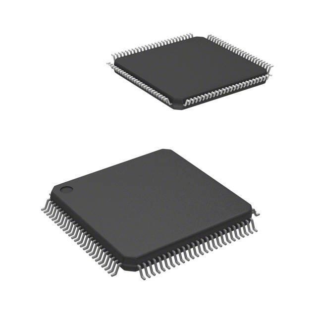


 工商网监
湘ICP备2023018690号
工商网监
湘ICP备2023018690号
