Please note that Cypress is an Infineon Technologies Company.
The document following this cover page is marked as “Cypress” document as this is the
company that originally developed the product. Please note that Infineon will continue
to offer the product to new and existing customers as part of the Infineon product
portfolio.
Continuity of document content
The fact that Infineon offers the following product as part of the Infineon product
portfolio does not lead to any changes to this document. Future revisions will occur
when appropriate, and any changes will be set out on the document history page.
Continuity of ordering part numbers
Infineon continues to support existing part numbers. Please continue to use the
ordering part numbers listed in the datasheet for ordering.
www.infineon.com
�CY9DF126 - Atlas
CY9DF126 Series
General Description
CY9DF126 series is based on Cypress’s advanced Arm architecture (32-bit with instruction pipeline for RISC-like performance).
Improvements compared to the previous generation include significantly improved performance at higher frequency, reduced power
consumption and faster start-up time.
For highest processing speed at optimized power consumption an internal PLL can be selected to supply the CPU with up to 128 MHz
operation frequency from an external resonator.
Note Arm, Cortex, Thumb and CoreSight are the trademarks of Arm Limited in the EU and other countries.
Note APIX® is a registered mark of INOVA Semiconductors GmbH.
Features
High-Performance/High Memory Content
Low Power
®
■ Arm
8KB D-Cache, 8KB I-Cache
32-Bit Armv7 architecture
■ 205 DMIPS
■ 2MB Internal Flash
■ 64KB Internal EEFlash (Data Flash)
■ 208KB Internal RAM with ECC
■
Connectivity
■
3x CAN, 2 x LIN-USART, 3 x SPI, 1 x I2C, 2 x I2S
■ Up to six Stepper Motor Control (SMC) outputs
■ HS-SPI (memory mapped access)
■ APIX 1 x PHY / 2 x AIC
■ External Bus Interface (24-bit address/16-bit data)
Characteristics
Cortex®-R4,
■
■
Safety Features/Security Features
■
■
■
■
■
■
■
■
5V capable IOs
Ta: 40 °C to +105 °C
Package: LQFP-176
Applications
■
Multiple Memory Production Units (MPU)
■ Peripheral Protection Units (PPU)
■ Timing Protection Unit (TPU)
■ CRC of Flash, Cache, and RAM
■ Watchdog
■ Flash-, Debug- and Test-Security
■
Switchable Power Domains
16KB Retention RAM
Flexible Clock Control
Debugging/Testing
Arm Coresight Debug and Trace
Debugging via JTAG Interface
Boundary Scan
■
■
Classical Automotive Instruments Cluster with pointers
Vehicle Controller for Virtual Cluster and Head Units in cards
APIX TX support 500, 250, 125 Mbps pixel data link transmission and 62.5, 41.67, 31.25, 20.83 Mbps sideband data
reception
Other Features
Up/Down Counters
Programmable Pulse Generators
■ ADC - 50 channels
■ Sound Generator
■ Free Running/Reload Timers
■ Real-Time Clock (RTC)
■ Input Capture Units, Output Compare units
■ 32 external Interrupts
■
■
Errata: For information on silicon errata, see “Errata” on page 291. Details include trigger conditions, devices affected, and proposed workaround.
Cypress Semiconductor Corporation
Document Number: 002-09314 Rev. *A
•
198 Champion Court
•
San Jose, CA 95134-1709
•
408-943-2600
Revised June 4, 2019
�CY9DF126 - Atlas
Block Diagram
Controlgroup
EBI0_MDATA00i......EBI0_MDATA15i
EBI0_RDY
EIC0_INT00.... EIC0_INT31
EIC
Memories
NMI
EIC0_NMI
RTC
RTC_WOT
SYSC
SYSC_CKOT
SYSC_CKOTX
TPU
IRQ Control
Power Control
RetRAM
16K
EEFlash
64K option
CLK_MEM_E_PD3
Watchdog
EBI0_MDATA00o...EBI0_MDATA15o
EBI0_MAD00...EBI0_MAD23
EBI0_MDQM0, EBI0_MDQM1
EBI0_MWEX
EBI0_MOEX
EBI0_MCLK
EBI0_MCASX
EBI0_MRASX
EBI0_MDWEX
EBI0_MCKE
EBI0_MNALE
EBI0_MNCLE
EBI0_MNWEX
EBI0_MNREX
EBI0_MCSX0...EBI0_MCSX3
EBI0_MCSX8
CLK_CFG_PD4
BootROM
8K
HS−SPI
(1 ch)
TCMRAM
128K
EBI
CLK_MEM_E_PD3
TCFlash
2M
ECC
CLK_HPM_PD2
SRAM
64K
Memory
Map
CLK_DBG_PD2
Clock group
Cortex R4
On−chip
Debug
I−Cache
8K
Trace
Oscillators
PLL’s
CLK_TRACE_PD2
D−Cache
8K
MPU
12 ch
CSV/CLK−out
CLK_SYS_PD3
CLK_CFG_PD1
High Performance Matrix (HPM)
CLK_HPM_PD2
GPIO0_00o˘GPIO0_52o
GPIO0_62o,GPIO0_63o
GPIO1_00o˘GPIO1_59o
GPIO2_00o˘GPIO2_25o
PPU
CLK_PERI4_PD2
CRC
I2S
(2 ch)
Remote
Handler
A−Shell 1
A−Shell 0
Peripheral Bus
Bridge 0
Peripheral Bus
Bridge 1
SPIn_CLKi
SPIn_DATA0i˘. SPIn_DATA3i
SPIn_SSi
SPIn_CLKo
SPIn_DATA[0]o˘. SPIn_DATA[3]o
SPIn_SSo
SPIn_SSO[1]˘. SPIn_SSO[3]
SG_SGA
SG_SGO
SG
(1 ch)
10−bit ADC
I2Sn_ECLK
I2Sn_SCKi
I2Sn_SDi
I2Sn_WSi
CANn_RX
CANn_TX
CAN
(3 ch)
I2Sn_SDo
I2Sn_WSo
I2Sn_SCKo
USART6_SCKi
USART6_SIN
USART6_SCKo
USART6_SOT
I/O Timer
(4 ch)
FRT 0/1/2/3
ICU 2/3
OCU 0/1
AIC0_dbg−select
ARH0−AIC0_RCK
ARH0_AIC0_RDA0
ARH0_AIC0_RDA1
ARH0_AIC0_TCKI
FRTn_FRCK
ICUn_IN0, ICUn_IN1
OTDn,OTDn_I,OTDn_G,OTDn_GI
ARH0_AIC0_UPCLK
ARH0_AIC0_UPDATA0
ARH0_AIC0_UPDATA1
PPG_ETRG0˘.. PPG_ETRG3
ARH0−AIC0_TDA0
PPGA
ARH0−AIC0_TDA1
PPGB
ARH0−AIC1_TDA0
ARH0−AIC1_TDA1
ARH0−AIC0_dbg_out_0, ARH0−AIC1_dbg_out_0
ARH0−AIC0_dbg_out_1, ARH0−AIC1_dbg_out_1
APIX
R
PHY
(50 ch)
USART
(1 ch)
I/O Timer
(4 ch)
FRT 16/17/18/19
ICU 18/19
OCU 16/17
SDINM/SDINP
SDOUTM/SDOUTP
PERI0_RBUS
GPIO0_00i˘... GPIO0_52i
GPIO0_62i,GPIO0_63i
GPIO1_00i˘...GPIO1_59i
GPIO2_00i˘... GPIO2_25i
CLK_HPM_PD2
PERI5_AHB BUS
DMA
(8 ch)
PERI1_RBUS
GPIO
(141 pins)
SPI
(3 ch)
UDC0_AIN0, UDC0_AIN1
UDC0_BIN0, UDC0_BIN1
UDC0_ZIN0, UDC0_ZIN1
UDC0_UDOT0
UDC0_UDOT1
DMA0_DEOP_ACK0, DMA0_DEOP_ACK1
DMA0_DREQ0, DMA0_DREQ1
DMA0_DSTP0, DMA0_DSTP1
DMA0_DREQ_ACK0, DMA0_DREQ_ACK1
DMA0_DSTP_ACK0, DMA0_DSTP_ACK1
DMA0_DEOP0, DMA0_DEOP1
16−bit PPG
(8 ch)
CLK_PERI0_PD2
UDC
(1 ch)
RLTn_TIN
RLTn_TOUT
PERI4_SLAVE AHB BUS
PERI3_eRBUS
RLT
(10 ch)
Peripheral Bus
Bridge 4
CLK_HPM_PD2
CLK_DMA_PD2
CLK_PERI1_PD2
CLK_HPM_PD2
Peripheral Bus
Bridge 3
CLK_PERI3_PD2
X0
X1
MODE
X0A
X1A
RSTX
DBG0_CTL
DBG0_CLK
DBG0_TRACE0.... DBG0_TRACE7
USART
(1 ch)
AVDD5
AVSS5
AVRH
ADC0_AN0..... ADC0_AN31
ADC0_EDGI
FRTn_FRCK
ICUn_IN0, ICUn_IN1
OTDn,OTDn_I,OTDn_G,OTDn_GI
USART0_SCKi
USART0_SIN
USART0_SCKo
USART0_SOT
I2C
(1 ch)
I2C0_SCLi
I2C0_SDAi
I2C0_SCLo
I2C0_SDAo
SMC
(6 ch)
SMCn_M1
SMCn_P1
SMCn_M2
SMCn_P2
16−bit PPG
(16 ch)
PPG_ETRG0˘.. PPG_ETRG3
PPGn_PPGA
PPGn_PPGB
Power Domain
Power Domain
Modules
PD1
Clockgroup (Osc, PLL, CSV), Controlgroup (EIC, NMI, RTC, SYSC, WDG, TPU, IRQ Control, Power Control)
PD2
Peripheral bus 0 (ADC, FRT, ICU, OCU, USART, I2C, SMC, PPG), Peripheral bus 1 (SG, CAN, USART, FRT,
ICU, OCU, PPG), Peripheral bus 3 (RLT, UDC, GPIO, PPU), Peripheral bus 4 (SPI, ARH, APIX, I2S), On-Chip
Debug, Trace, SRAM, CRC
PD3
Cortex R4, MPU, I-Cache, D-Cache, TCM, TCFlash, EEFlash, TPU, BootROM, HS-SPI, EBI
PD4
RetRAM
Document Number: 002-09314 Rev. *A
Page 2 of 336
�CY9DF126 - Atlas
Contents
CY9DF126 Overview and Features ................................. 4
Resource Distribution for Non-Modulated Clock ....... 14
Lock/Unlock Values for Protection Units ................... 14
ID-Values for Module Identification Registers ........... 15
Package and Pin Assignment ....................................... 16
Package .................................................................... 16
IO Circuit Types ......................................................... 21
I/O Pins and Functions .............................................. 25
Interrupt / DMA ................................................................ 66
NMI ............................................................................ 72
DMA Overview .......................................................... 73
PPU ........................................................................... 77
Master ID ................................................................... 78
I/O Map ............................................................................. 79
Electrical Characteristics ............................................. 236
Absolute Maximum Ratings ..................................... 236
Recommended Operating Conditions ..................... 240
DC Characteristics ................................................. 241
AC Characteristics ................................................... 247
Analog Digital Converter ......................................... 264
FLASH Memory Program/Erase Characteristics
for TCFLASH and EEFLASH .................................. 267
RC Oscillator Frequency ......................................... 268
ESD Structure between Power Domains ................ 270
Procedures .................................................................... 272
Boundary scan ........................................................ 272
Flash Parallel Programming .................................... 274
Memory Map ........................................................... 279
Debug and Trace ..................................................... 285
Handling Devices .......................................................... 287
Preventing Latch-up ................................................ 287
Document Number: 002-09314 Rev. *A
Handling of Unused Input Pins ................................ 287
Power Supply Pins .................................................. 287
Power on Sequence ................................................ 287
Pin State while Power-On-Reset ............................. 288
Crystal Oscillator Circuit .......................................... 289
Notes on using External Clock ................................ 289
Errata ............................................................................. 291
Ordering Information .................................................... 312
Appendix ....................................................................... 313
Workaround for Flash Erase Suspend Issue ........... 313
Workaround for TCFlash TCM Access .................... 314
Workaround for TCFlash AXI Access ...................... 316
Workaround for External Bus Hang-Up ................... 318
Workaround for EEFlash Single Bit ECC Error ....... 318
Workaround for IRQ Unit Register Read
Timing Issue ............................................................ 319
Workaround for IUNIT Interrupt
Handling Problem .................................................... 326
Rootcause for APIX VDDA Current Problem .......... 328
Workaround for APIX VDDA Current Problem ........ 329
Limitation for Undefined Port Pin State
while Core Supply (VDD) is Unavailable ................. 330
Document History Page ............................................... 333
Document History ......................................................... 334
Sales, Solutions, and Legal Information .................... 336
Worldwide Sales and Design Support ..................... 336
Products .................................................................. 336
PSoC® Solutions .................................................... 336
Cypress Developer Community ............................... 336
Technical Support ................................................... 336
Page 3 of 336
�CY9DF126 - Atlas
CY9DF126 Overview and Features
Table 1. Overview
Feature
CY9DF126 / QFP-176
Max. Core frequency
128 MHz
DMA
8 channels
TCFlash
2 MB
EEFlash
64 KB
AXI RAM (with ECC)
64 KB
TCM RAM (with ECC)
128 KB
RetRAM
16 KB
Core has 4-way-associative cache
I/D each 8KB
Boot-ROM
8 KB
IRQ Ctrl
256
RTC (with auto calibration)
1 channel
Source clock timer
4
RLT (Reload Timer) (32 bit)
10 channels
FRT
8 channels
ICU
8 channels
OCU
8 channels
PPG
24 channels
SG (Sound Generator)
1 channel
UDC (UpDown Counter)
2 channels
CAN
3 channels
USART (LIN-USART)
2 channels
SPI
3 channels
I2C
1 channel
I2S
2 channels
ARH (Automotive Remote Handler)
2 channels (1 channel physical)
Quad - SPI
1 channel
External bus
24-bit address/16-bit data
EIC (External Interrupts)
32 channels
NMI (intern / extern)
32/1
SMC
6 channels
ADC (10-bit)
50 channels (including 24 channels shared with SMC)
CRC
1 channel
Package
QFP-176
Document Number: 002-09314 Rev. *A
Page 4 of 336
�CY9DF126 - Atlas
Table 2. Feature
Feature
Technology
Description
■ 90nm CMOS with embedded flash
■ Cortex R4 CPU core
■ 32-bit Arm architecture, dual-issue superscalar eight stage pipeline
■ Armv7 and Thumb-2 instruction set compliant
■ Memory Protection Unit (MPU) with 12 regions
■ Two Tightly Coupled Memory (TCM) ports. 64-bit AXI slave port for access to TCMs
Processor Subsystem
■ 64-bit AXI master port
■ Vectored Interrupt Controller (VIC) port for faster interrupt processing
■ Single error correction, double error detection (SECDED) Error Correction Coding (ECC) for memory error detection
and correction
■ Instruction cache: 8KB 4-way set-associative
■ Data cache: 8KB 4-way set-associative
■ Up to 8 break-points and 8 watchpoints
■ Arm Coresight technology
Debug and Trace
■ Standard 5-pin JTAG interface
■ 4-bit, 8-bit, 16-bit, and 32-bit trace data width supported depending on package
■ Secure entry supported for debugger
■ External main clock of 4MHz (up to 8MHz under evaluation)
■ External sub clock (typical 32.768 kHz)
Clocks
■ Embedded RC oscillator (typical 8/12 MHz, configurable)
■ Embedded Slow RC oscillator (typical 100 kHz)
■ On-chip Phase Locked Loop (PLL) clock multiplier for main clock, Spread Spectrum Clock Generation (SSCG)
■ Stabilization timers for all source clocks
Clock Supervisor
■ Clock supervision for all source clocks and PLL outputs
■ Reset generation for out-of-bound clock frequencies on input source clocks, or PLL output clocks
■ Power on Reset (PoR)
■ External Reset
■ Software triggered hard reset
Resets
■ Clock supervision resets
■ Watchdog
■ Low Voltage Detection reset
■ Software reset
■ 32-bit counter
■ Supports selection of four clock sources (Main clock, Sub clock, RC clock or Slow RC clock)
■ Support for window watchdog functionality
Watchdog Timer
■ Reset or NMI generation support on watchdog errors
■ Support for preemptive warning interrupt before watchdog reset or NMI generation
■ Additional safety provision through three times redundancy and error correction logic for important configuration bits
■ Option to halt watchdog counter in case of core reaching break-point
Document Number: 002-09314 Rev. *A
Page 5 of 336
�CY9DF126 - Atlas
Table 2. Feature (Continued)
Feature
Description
■ 64-bit AHB Master Interface
■ 32-bit AHB Slave Interface
■ Block, burst and demand transfer modes
DMA
■ Fixed and incremental addressing for source as well as destination
■ 132 clients
■ 8 channels to handle independent data flows
■ Fixed priority, dynamic priority, and round robin arbitration
■ Interrupt Request (IRQ) and Fast Interrupt Request (FIQ) capability
■ NMI sources can generate FIQ
■ Supports 32 Non Maskable Interrupt (NMI) source for FIQ generation
■ Supports 512 Normal Interrupt sources for IRQ generation
Interrupts
■ Supports request for low power mode entry
■ Programmable 32-level priority controller for normal IRQ sources. Also, supports programmable priority level masking
■ Programmable 16-level priority controller for NMI interrupt sources
■ Software interrupt generation
■ Privileged mode support for restricted access
■ Up to 32 pins can be used as external interrupts
■ Optional 25ns (typical) noise filters on all lines
■ DMA support
External Interrupts
■ NMI support
■ Five polarity support (‘H’, ‘L’, rising edge, falling edge, and, any edge)
■ Event capture support for all 32 external interrupt pins
■ Software enabled monitoring of external events, with sampling frequency of 500Hz to 16MHz
■ Up to eight identical 24-bit timers for execution time protection, locking time protection, inter-arrival time protection
or deadline protection
Timing Protection
■ Normal and overflow mode support
■ Global linear prescaler (1 to 64) to scale down clock frequency
■ Additional, individual timer prescaler to support 4 different software programmable frequencies (1, 1/2, 1/4, and 1/16 )
■ Start, stop, and continue options per timer controllable by software
■ Memory protection unit for all bus masters
Memory Protection
■ AXI interface support
■ 8 programmable memory regions, and one background region which covers entire 4GB address space
■ Unauthorized access generates NMI
■ Protection to all peripherals and General Purpose IOs (GPIO)
Peripheral Protection
■ Individual protection setting for up to 512 peripherals, and 512 GPIO channels
■ DMA access support for faster register configuration
■ Supports CAN protocol version 2.0 part A and B
■ Bit rates up to 1 Mbps
■ 64 message objects
CAN
■ Each message object has its own identifier mask
■ Programmable FIFO mode (concatenation of message objects)
■ Maskable interrupt
■ Disabled automatic retransmission mode for time triggered CAN applications
■ Programmable loop-back mode for self-test operation
Document Number: 002-09314 Rev. *A
Page 6 of 336
�CY9DF126 - Atlas
Table 2. Feature (Continued)
Feature
Description
■ Programmable LIN or USART function
■ Full-duplex support
■ Clock synchronous (start-stop synchronization and start-stop-bit option),and Clock asynchronous (using start-,
stop-bits) transfer modes
■ Dedicated baud rate generator. Mechanism for automatic baud rate adjust available in LIN mode
USART/LIN
■ Support for data length of 7-bits (not in synchronous or LIN mode) and 8-bits
■ Support for signal modes Non-Return to Zero (NRZ) and Non-Return to Zero Inverted (NRZI)
■ Reception error detection for framing, overrun, parity, checksum, sync field timeout, and frame-ID (only in LIN mode)
errors
■ Interrupt capability for transmission, reception, and errors
■ DMA support
■ Master/slave transmitting and receiving functions
■ 7-bit addressing as master and slave
■ 10-bit addressing as master and slave
I2C
■ Acknowledge disable option upon slave address reception (master-only operation)
■ Address mirroring to give interface several slave addresses
■ Up to 400 kbps transfer rate
■ Optional noise filters for SDA and SCL
■ Interrupt capability on transmission and bus error events
■ PWM duty cycle programmable from 0% to 100%
Stepper Motor Control
■ Programmable setting to select ‘L’, ‘H’, ‘PWM’ and ‘HighZ’ output
■ High current output pins
■ 50 channels
■ Conversion time: 1us per channel
■ RC type Successive Approximation (SAR) with sample and hold circuit
■ 10-bit or 8-bit resolution
A/D Converter
■ Program selection analog input from 32 channels
■ Single conversion, continuous conversion, and scan conversion options
■ Interrupt capability
■ DMA support
■ 4 range comparator channels for comparing conversion output with thresholds
■ Programmable master/slave operations
■ Supports transmission only, reception only and simultaneous transmission/reception operations
■ Support for 1 sub frame and 2 sub frame constructions
■ Up to 32 channels supported in each sub frame
■ Support for individual configuration of channel number, channel length, word length in each sub frame
I2S
■ Word length support from 7-bits to 32-bits
■ Programmable frequency, polarity, and phase of frame synchronous signal
■ Programmable sampling point of received data (center or at the end of received data)
■ Support for frequency division from 1 to 126 in multiples of 2
■ DMA support
■ Interrupt capability
Document Number: 002-09314 Rev. *A
Page 7 of 336
�CY9DF126 - Atlas
Table 2. Feature (Continued)
Feature
Description
■ Produces sound/melody with varying frequency and amplitude
■ Square wave sound output with frequency of 100Hz – 6kHz (resolution 20Hz)
■ Programmable Pulse Width Modulated (PWM) cycle width of 255 or 511 clocks. PWM duty cycle programmable from
0% to 100%
Sound Generator
■ Two 2-bit prescaler with programmable clock division of 1, 1/2, 1/3, and 1/4
■ Automatic linear or exponential amplitude increment or decrement
■ Start, stop, resume functionality
■ DMA support
■ Automatic sound output stop when amplitude becomes 0
■ Format: 32-bit or 2 times 16-bit
■ Three count modes (timer mode, up/down count mode, and phase difference count mode) supported
■ Multiply by 2 or multiply by 4 in phase difference count mode
Up Down Counter
■ Count source can be internal clock or external trigger
■ Counting range: any value between 0 and 232-1 can be set
■ 4 interrupt options (Compare-match interrupt, Underflow interrupt, Overflow interrupt, and Count direction change
interrupt)
■ 32-bit reload counter
■ External and Internal clock/event source
■ Trigger signal programmable as rising/falling edge or both
■ Gated count function
Reload Timers
■ One-shot or reload counter mode
■ Counter state can be made visible at external pin
■ Prescaler with six different settings for the internal clock and two settings for the external clock
■ Several Reload Timers can be cascaded to form a longer Reload Timer
■ DMA support
■ Signals an interrupt on overflow, match with Compare registers, zero-detection, or match with Compare Clear
Register
■ Option to mask zero detection, compare clear match interrupt, or both to allow for interrupt generation only after
multiple events
Free Running Timers
■ Programmable timer period up to 1 s
■ Support for 11 counter clocks. Prescaler with 1, 1/2, 1/4, 1/8, 1/16, 1/32, 1/64, 1/128, 1/256, 1/512, and 1/1024 of
peripheral clock frequency
■ DMA support
■ Consists of 2 independent input channels
■ 16-bit wide capture registers per channel
Input Capture Units
■ Signals an interrupt upon external event
■ Rising edge, falling edge or rising & falling edge sensitive
■ DMA support
■ Consists of 2 independent channels
■ 16-bit wide
Output Compare Units
■ Signals an interrupt when a match with 16-bit I/O Timer occurs
■ A pair of compare registers can be used to generate an output signal
■ Interrupt capability
Document Number: 002-09314 Rev. *A
Page 8 of 336
�CY9DF126 - Atlas
Table 2. Feature (Continued)
Feature
Description
■ 16-bit down counter, cycle and duty setting registers
■ Interrupt at trigger, counter borrow and/or duty match
Programmable Pulse
Generator
■ PWM operation and one-shot operation
■ Internal prescaler allows 1, 1/4, 1/16, 1/64 of peripheral clock as counter clock and Reload timer underflow as clock
input
■ Can be triggered by software or reload timer
■ Can be clocked from main clock, sub clock or RC clock
■ Automatic calibration support even when device is in low power state
■ Interrupt capability on half-second, 1 second, 1 minute, 1 hour, and 1 day duration
Real Time Clock
■ Additional capability for interrupt generation on calibration failure detection and calibration done event
■ Auto calibration of Sub clock or RC clock with respect to Main clock
■ Separate clock selector for calibration
■ Configurable calibration duration
■ Auto/manual trigger for calibration
■ 128 KB
Internal Memories- TCMRAM ■ 64-bit interface
■ Single error correction, double error detection (SECDED) ECC support
■ 64-bit AXI interface
Internal Memories- System ■ 64 KB
RAM
■ Single error correction, double error detection (SECDED) ECC support
■ Parallel read/write capability for 2 different banks
■ 16 KB
Internal Memories- Retention ■ 4 banks
RAM
■ 32-bit AHB
■ Low leakage RAMs for low power consumption
■ 2 MB
■ Parallel Programming support
■ Mapped to TCM address space as well as Cacheable address space through AXI interface
■ Single error correction, double error detection (SECDED) ECC support
Tightly Coupled Flash
Memory
■ TCM address space supports only read access
■ Cacheable AXI address space supports write and read access
■ Detection of hang-up 1 state
■ 32 large sectors of 64KB each
■ 16 small sectors of 8KB each
■ Sector-wise access protection for write and read accesses
■ 64 KB
■ Parallel Programming support
■ Single error correction, double error detection (SECDED) ECC support
EEPROM Emulation Flash
Memory
■ Support for sector erase
■ EEPROM emulation mode support
■ Support for mirroring of memory in 3 diverse memory-mapped regions
■ 8 sectors of 8KB each
■ Sector-wise access protection for write and read accesses
Document Number: 002-09314 Rev. *A
Page 9 of 336
�CY9DF126 - Atlas
Table 2. Feature (Continued)
Feature
Description
■ Supports legacy as well as the dual-bit and quad-bit modes of SPI operation
■ Supports up to four slave devices in master mode
Quad SPI
■ Programmable transfer rate, active-level of slave-select signal, polarity, and phase of the serial clock per slave select
■ Support for memory mapped operation of external serial flash and serial SRAM devices in command sequencer mode
■ Additional direct mode support for standard SPI operation through FIFO interface
Error Collection
■ Error collection on all peripherals
■ Optional Non-Maskable Interrupt (NMI) generation capability
■ Low voltage detection for 5V, 3.3V, and 1.2V
Low Voltage Detect
■ Programmable thresholds
■ Reset generation capability on low voltage events
■ All functional pins can be used as GPIO
I/O Ports
■ Programmable analog or digital functionality selection
■ Programmable input levels (Automotive, CMOS, and TTL)
■ Programmable pull-up/pull-down and output drive
■ Endianess configuration support for all SRAM interfaces based on chip select
EBI
■ PPU Protection for EBI Configuration register range
■ Only 32-bit write access support supported by EBI Configuration registers
■ Lock/Unlock register for write protection for EBI Configuration registers
■ Support 500, 250, 125 Mbps pixel data transmission
APIX
■ Support 62.5, 41.67, 31.25, 20.83 Mbps side band data reception
■ Support loop back test mode (BIST logic)
■ Monitoring PLL lock detection over Osc clock glitches
■ PPU protection for register access
■ Debug support for RAM
ARH
■ Registers accesses based on Lock status ARHn_RHCTRL:LST bit, ARHn_TST:TM bit, on transaction buffer state,
and on tx_config from Remote Handler
■ Arbitration between S/W read and A-Shell write over the event buffer
■ Programmable 8, 16, 24 or 32 bit input data width
■ Programmable polynomial value (Polynomial degree from 2 to 32)
■ Programmable initial seed value
CRC
■ Programmable final checksum XOR value
■ Interrupt and DMA client interface
■ Configurable input/output bit reflection and byte swapping
■ Supports PPU
■ Supports block/multiple data transfers (more than 32-bit)
Packages
QFP-176 (series variant)
Note EEPROM (Electronically Erasable and Programmable Read-Only Memory)
Document Number: 002-09314 Rev. *A
Page 10 of 336
�CY9DF126 - Atlas
Table 3. Memory Map (Continued)
Table 3. Memory Map
Start Address
Module
Start Address
Module
01000000
AXI_FLASH_MEMORY_LARGE_SECTORS
00FE0000
TCM_FLASH_SMALL_SECTORS
00A00000
Reserved
00800000
TCM_FLASH_LARGE_SECTORS
FFFF2000
Reserved
FFFF0000
BOOTROM
FFFEF000
EXCFG
B0D01000
Reserved
B0D00000
SYSTEM_RAM_CONFIG
B0C00000
PERI5_AHB
00020000
Reserved
B0B00000
PERI4_SLAVE
00000000
TCM_RAM
B0A00000
PERI3_ERBUS
B0900000
Reserved
B0800000
PERI1_RBUS
B0700000
PERI0_RBUS
Start Address
Module
B0600000
MCU_CONFIG
B0500000
DEBUG_BUS
B0400000
MEMORY_CONFIG
B0200000
Reserved
B07FFC00
B07FA800
B07F8000
B07F0400
B07F0000
B07EC000
B07E8000
B075A000
B074C000
B074BC00
B0748C00
B0748800
B0748400
B0748000
B0747C00
B073BC00
B073B800
B073B400
B073B000
B073AC00
B073A800
B073A400
B073A000
B0739C00
B0739800
B0739400
B0739000
B0738C00
B0738800
B0738400
B0738000
B0732000
B0731800
BSU0
Reserved
RICFG0
Reserved
BECU0
Reserved
PPC
Reserved
PPGGLC0
Reserved
PPGGRP3
PPGGRP2
PPGGRP1
PPGGRP0
Reserved
PPG15
PPG14
PPG13
PPG12
PPG11
PPG10
PPG9
PPG8
PPG7
PPG6
PPG5
PPG4
PPG3
PPG2
PPG1
PPG0
Reserved
SMCTG0
B0180000
EBI
B0080000
Reserved
B0000000
HSSPI0
90000000
Reserved
80000000
HSSPI0_MEMORY
28000000
Reserved
20000000
EBI_MEMORY1
10000000
EBI_MEMORY0
06000000
Reserved
05FE0000
AXI_SLAVE_CORE0_TCM_FLASH_SMALL_SECTORS
05A00000
Reserved
05800000
AXI_SLAVE_CORE0_TCM_FLASH_LARGE_SECTORS
05020000
Reserved
05000000
AXI_SLAVE_CORE0_TCM_RAM
04800000
AXI_SLAVE_CORE0_DCACHE
04000000
AXI_SLAVE_CORE0_ICACHE
01A10000
Reserved
01A00000
SYSTEM_RAM
01800000
Reserved
017E0000
AXI_FLASH_MEMORY_SMALL_SECTORS
01200000
Reserved
Document Number: 002-09314 Rev. *A
Table 4. PERI0_RBUS Memory Map
Page 11 of 336
�CY9DF126 - Atlas
Table 4. PERI0_RBUS Memory Map (Continued)
Table 5. PERI1_RBUS Memory Map (Continued)
Start Address
Module
Start Address
Module
B0731400
B0731000
B0730C00
B0730800
B0730400
B0730000
B0729800
B0728000
B0720C00
B0720000
B071C000
B0718400
B0718000
B0714000
B0710C00
B0710800
B0710400
B0708C00
B0708800
B0708400
B0708000
B0700400
B0700000
SMC5
SMC4
SMC3
SMC2
SMC1
SMC0
Reserved
USART0
Reserved
I2C0
Reserved
OCU1
OCU0
Reserved
ICU3
ICU2
Reserved
FRT3
FRT2
FRT1
FRT0
Reserved
ADC0
B0838000
B0830C00
B0828400
B0828000
B0824000
B0820C00
B0820800
B0820400
B0818C00
B0818800
B0818400
B0818000
B0810400
B0808800
B0808400
B0808000
B0800400
B0800000
USART6
Reserved
OCU17
OCU16
Reserved
ICU19
ICU18
Reserved
FRT19
FRT18
FRT17
FRT16
Reserved
CAN2
CAN1
CAN0
Reserved
SG0
Table 5. PERI1_RBUS Memory Map
Table 6. PERI3_eRBUS Memory Map
Start Address
Module
B0AFFC00
BSU3
B0AF9400
Reserved
B0AF8000
RICFG3
Start Address
Module
B0AF0000
BECU3
B08FFC00
B08FB000
B08F8000
B08F0000
B0868000
B085C000
B085BC00
B0858400
B0858000
B0857C00
B0849C00
B0849800
B0849400
B0849000
B0848C00
B0848800
B0848400
B0848000
B0842000
BSU1
Reserved
RICFG1
BECU1
Reserved
PPGGLC1
Reserved
PPGGRP17
PPGGRP16
Reserved
PPG71
PPG70
PPG69
PPG68
PPG67
PPG66
PPG65
PPG64
Reserved
B0A28000
Reserved
B0A20000
UDC0
B0A18000
Reserved
B0A12400
RLT9
B0A12000
RLT8
B0A11C00
RLT7
B0A11800
RLT6
B0A11400
RLT5
B0A11000
RLT4
B0A10C00
RLT3
B0A10800
RLT2
B0A10400
RLT1
B0A10000
RLT0
B0A09000
Reserved
B0A08000
GPIO
Document Number: 002-09314 Rev. *A
Page 12 of 336
�CY9DF126 - Atlas
Table 6. PERI3_eRBUS Memory Map (Continued)
Start Address
Module
B0A00400
Reserved
B0A00000
PPU0
Table 7. PERI4_SLAVE AHB Bus Memory Map
Table 9. Memory and Config (MEMORY_CONFIG) AHB Bus
Memory Map (Continued)
Start Address
Module
B0440000
EEFLASH_ECC_MIR
B0420400
Reserved
B0418000
BSU6
B0412400
Reserved
Start Address
Module
B0BFFC00
BSU4
B0412000
EEFCFG
B0BFA400
Reserved
B0411400
Reserved
B0BF8000
RICFG4
B0411000
TCFCFG
B0B40400
Reserved
B0B40000
ARH0
B0410400
Reserved
B0B3B000
Reserved
B0410000
TRCFG
B0B38800
SPI2
B040B400
Reserved
B0B38400
SPI1
B0408000
TPU0
B0B38000
SPI0
B0401000
Reserved
B0B30800
Reserved
B0B30000
CRC0
B0400000
IRQ0
B0B29000
Reserved
B0B20400
I2S1
B0B20000
I2S0
Start Address
B0B00000
Reserved
B06FFC00
BSU7
B06F9400
Reserved
B06F8000
RICFG7
B0648000
Reserved
B063B000
RETRAMBANK3
B063A000
RETRAMBANK2
B0639000
RETRAMBANK1
B0638000
RETRAMBANK0
B0630000
Reserved
B0628000
EICU0
B0620400
Reserved
B0620000
EIC0
B0618400
Reserved
B0618000
RTC
B0610400
Reserved
Table 8. PERI5_AHB Bus Memory Map
Start Address
Module
B0CFFC00
BSU5
B0CFF800
Reserved
B0C08000
MPUXDMA0
B0C04000
Reserved
B0C00000
DMA0
B0800000
PERI1_RBUS
B0700000
PERI0_RBUS
Table 9. Memory and Config (MEMORY_CONFIG) AHB Bus
Memory Map
Table 10. MCU_CONFIG AHB Bus Memory Map
Module
Start Address
Module
B0610000
RRCFG
B04C0000
EEFLASH_NOECC_MIR
B0608400
Reserved
EEFLASH_TABLE_MIR
B0608000
WDG
B0480000
Document Number: 002-09314 Rev. *A
Page 13 of 336
�CY9DF126 - Atlas
Table 10. MCU_CONFIG AHB Bus Memory Map (Continued)
Start Address
Module
B0601000
Reserved
B0600000
SYSC
Lock/Unlock Values for Protection Units
For various protection and system relevant units, registers must
be unlocked before configuring and can be locked for protection.
For the details about functionality, see the FCR4 Hardware
Manual.
Table 14. Lock/unlock Values for FCR4 Protection Module
Instances
Table 11. HSSPI0 Memory Map
Module
Unlock value
Lock value
TPU0
ACC5A110
B10CACC5
Start Address
Module
B007FC00
BSU8
PPU0
ACC5BB01
BB0B10C1
B0078400
Reserved
MPUXDMA0
ACCABB56
112ABB56
B0078000
RICFG8
TRCFG
ACC55ECC
5ECCB10C
B0000000
HSSPI0
EXCFG
ACC5B007
B007ECF6
Table 12. EBI Memory Map
IRQ0
17ACC911
17B10C11
RRCFG
ACC5DECC
DECCB10C
SCCFG
5ECACCE5
A135331A
551FB10C
Start Address
Module
SRCFG
5ECC551F
B01FFC00
BSU10
ARH0
A86ACCE5
A86AB10C
B0180080
Reserved
ETH0
E18ACCE5
E18B10CC
B0180000
EBI
TCFCFG
CF61F1A5
-
EEFCFG
CF6DF1A5
Resource Distribution for Non-Modulated Clock
WDG
EDACCE55
-
Some of the resources are available with modulated and
non-modulated clock. Find below the distribution:
SYSC
5CACCE55
-
EBI
EB1410CE
10CE0EB1
Table 13. Resource Distribution for Non-Modulated Clock
Module
Non-Modulated
Modulation
Possible
CAN
3
-
SG
1
-
ICU/OCU/FRT
4
4
PPG
8
16
USART/LIN
1
1
I2C
1
-
SMC
-
6
Document Number: 002-09314 Rev. *A
Page 14 of 336
�CY9DF126 - Atlas
ID-Values for Module Identification Registers
For several peripheral and system related modules, the hardware contains Module Identification Registers that hold read-only values
which contain information about the module number, the version and possible patches.
Table 15. List of Module ID
Module
ID-Register
ID Value
System Controller
SYSC_SYSIDR
0x00020101
Security Checker
SCCFG_MODID
0x00020200
SRAM Interface
SRCFG_MID
0x00040200
TC-Flash Interface
TCFCFG_FMIDR
0x000E0102
EE-Flash Interface
EEFCFG_MIR
0x00090200
Interrupt Controller 0
IRQ0_MID
0x000B0100
DMA Controller 0
DMA0_ID
0x00010102
Timing Protection Unit 0
TPU0_MID
0x00050200
Memory Protection Unit for AXI
MPUXDMA0_MID
0x000D0100
Bus Error Collection Unit 0
BECU0_MIDH / BECU0_MIDL
0x0008 / 0x0100
Bus Error Collection Unit 1
BECU1_MIDH / BECU1_MIDL
0x0008 / 0x0100
Bus Error Collection Unit 3
BECU3_MIDH / BECU3_MIDL
0x0008 / 0x0100
High Speed SPI Interface 0
HSSPI0_MID
0x00060200
SPI Interface 0
SPI0_MID
0x00070200
SPI Interface 1
SPI1_MID
0x00070200
SPI Interface 2
SPI2_MID
0x00070200
Inter IC Sound 0
I2S0_MIDREG
0x000A0200
Inter IC Sound 1
I2S1_MIDREG
0x000A0200
Automotive Remote Handler 0
ARH0_MID
0x000C0200
Document Number: 002-09314 Rev. *A
Page 15 of 336
�CY9DF126 - Atlas
Package and Pin Assignment
Package
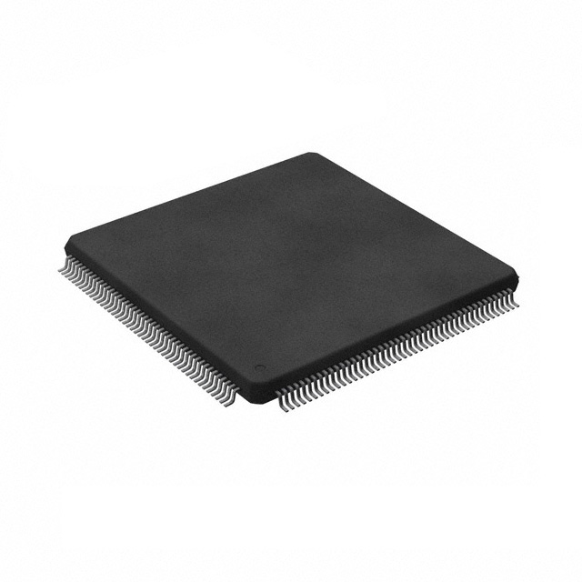
A QFP-176 package will be used for ATLAS. The Cypress code is LQP176.
132
131
130
129
128
127
126
125
124
123
122
121
120
119
118
117
116
115
114
113
112
111
110
109
108
107
106
105
104
103
102
101
100
99
98
97
96
95
94
93
92
91
90
89
VDP5
RSTX
MODE
X1A
X0A
VSS
XTAL0
XTAL1
VSSA
VDE5_OSC (5V)
VSSA
VDDA(1.2V)
VSSA
VDEA_VCO (3.3V
RREF
VDEA (3.3V)
SDOUTP
VSSA
SDOUTM
VDEA (3.3V)
SDINM
SDINP
VSSA
VDP3
VSS
P1_29
P1_28
P1_27
P1_26
P3_32
P3_31
P3_30
P3_29
P3_28
P3_27
P3_26
P3_25
VSS
VDP3
P3_24
P3_23
P3_22
VSS
VDD
Figure 1. QFP-176 Package
VDP5 / 3V−5V−IO
VDP5
APIX / analog
VDP3 / 3V−IO
QFP176
VDP5
133
134
135
136
137
138
139
140
141
142
143
144
145
146
147
148
149
150
151
152
153
154
155
156
157
158
159
160
161
162
163
164
165
166
167
168
169
170
171
172
173
174
175
176
VDP3 / 3V−IO
VSS
VDD
VSS
P0_40
P0_41
P0_42
P0_43
P0_44
P0_45
P0_46
P0_47
P0_48
P0_49
P0_50
P0_51
P0_62
P0_63
P2_32
P2_33
VDP5
VSS
P2_34
P2_35
P2_36
P2_37
P2_38
P2_39
P2_40
P2_41
P2_42
P2_43
P2_44
P2_45
P2_46
P2_47
VSS
VDP5
JTAG_TDO
JTAG_TDI
JTAG_TCK
VSS
VDD
JTAG_TMS
JTAG_NTRST
DVCC / 3V−5V−IO
VDP3 / 3V−IO
P3_21
P3_20
P3_19
P3_18
P3_17
P3_16
P3_15
P3_14
P3_13
VSS
VDP3
P3_42
P3_41
P3_40
P3_39
P3_38
P3_37
P3_36
P3_35
P3_34
P3_33
P1_25
P1_24
VDP3
VSS
P3_12
P3_11
P3_10
P3_09
P3_08
P3_07
P3_06
P3_05
P3_04
P3_03
P3_02
P3_01
VSS
VDP3
P3_00
P1_33
P1_32
P1_31
P1_30
AVSS5
AVRH5
AVDD5
DVCC
DVSS
P1_00
P1_01
P1_02
P1_03
P1_04
P1_05
P1_06
P1_07
DVSS
DVCC
P1_08
P1_09
P1_10
P1_11
P1_12
P1_13
P1_14
P1_15
DVSS
DVCC
P1_16
P1_17
P1_18
P1_19
P1_20
P1_21
P1_22
P1_23
DVSS
DVCC
VDP3
VSS
P1_34
P1_35
P1_36
P1_37
P1_38
VDD
VSS
1
2
3
4
5
6
7
8
9
10
11
12
13
14
15
16
17
18
19
20
21
22
23
24
25
26
27
28
29
30
31
32
33
34
35
36
37
38
39
40
41
42
43
44
analog
88
87
86
85
84
83
82
81
80
79
78
77
76
75
74
73
72
71
70
69
68
67
66
65
64
63
62
61
60
59
58
57
56
55
54
53
52
51
50
49
48
47
46
45
Document Number: 002-09314 Rev. *A
Page 16 of 336
�CY9DF126 - Atlas
Table 16. QFP-176 Package Pinout (Continued)
Table 16. QFP-176 Package Pinout
Pin No
Pin Name
IO_Type
1
AVSS5
supply
2
AVRH5
supply
3
AVDD5
supply
4
DVCC
supply
5
DVSS
supply
6
P1_00
SMC
7
P1_01
SMC
8
P1_02
SMC
9
P1_03
SMC
10
P1_04
SMC
11
P1_05
SMC
12
P1_06
SMC
13
P1_07
SMC
14
DVSS
supply
15
DVCC
supply
16
P1_08
SMC
17
P1_09
SMC
18
P1_10
SMC
19
P1_11
SMC
20
P1_12
SMC
21
P1_13
SMC
22
P1_14
SMC
23
P1_15
SMC
24
DVSS
supply
25
DVCC
supply
26
P1_16
SMC
27
P1_17
SMC
28
P1_18
SMC
29
P1_19
SMC
30
P1_20
SMC
31
P1_21
SMC
32
P1_22
SMC
33
P1_23
SMC
34
DVSS
supply
35
DVCC
supply
36
VDP3
supply
37
VSS
supply
38
P1_34
BIDI33
39
P1_35
BIDI33
Document Number: 002-09314 Rev. *A
Pin No
Pin Name
IO_Type
40
P1_36
BIDI33
41
P1_37
BIDI33
42
P1_38
BIDI33
43
VDD
supply
44
VSS
supply
45
P1_30
BIDI33
46
P1_31
BIDI33
47
P1_32
BIDI33
48
P1_33
BIDI33
49
P3_00
BIDI33
50
VDP3
supply
51
VSS
supply
52
P3_01
BIDI33
53
P3_02
BIDI33
54
P3_03
BIDI33
55
P3_04
BIDI33
56
P3_05
BIDI33
57
P3_06
BIDI33
58
P3_07
BIDI33
59
P3_08
BIDI33
60
P3_09
BIDI33
61
P3_10
BIDI33
62
P3_11
BIDI33
63
P3_12
BIDI33
64
VSS
supply
65
VDP3
supply
66
P1_24
BIDI33
67
P1_25
BIDI33
68
P3_33
BIDI33
69
P3_34
BIDI33
70
P3_35
BIDI33
71
P3_36
BIDI33
72
P3_37
BIDI33
73
P3_38
BIDI33
74
P3_39
BIDI33
75
P3_40
BIDI33
76
P3_41
BIDI33
77
P3_42
BIDI33
78
VDP3
supply
79
VSS
supply
Page 17 of 336
�CY9DF126 - Atlas
Table 16. QFP-176 Package Pinout (Continued)
Table 16. QFP-176 Package Pinout (Continued)
Pin No
Pin Name
IO_Type
Pin No
Pin Name
IO_Type
80
P3_13
BIDI33
120
VSSA
supply
81
P3_14
BIDI33
121
VDDA(1.2V)
supply
82
P3_15
BIDI33
122
VSSA
supply
83
P3_16
BIDI33
123
VDE5_OSC (5V)
supply
84
P3_17
BIDI33
124
VSSA
supply
85
P3_18
BIDI33
125
XTAL1
MAINOSC (20MHz)
86
P3_19
BIDI33
126
XTAL0
MAINOSC (20MHz)
87
P3_20
BIDI33
127
VSS
supply
88
P3_21
BIDI33
128
X0A
SUBOSC
89
VDD
supply
129
X1A
SUBOSC
90
VSS
supply
130
MODE
MODE
91
P3_22
BIDI33
131
RSTX
MODE
92
P3_23
BIDI33
132
VDP5
supply
93
P3_24
BIDI33
133
VSS
supply
94
VDP3
supply
134
VDD
supply
95
VSS
supply
135
VSS
supply
96
P3_25
BIDI33
136
P0_40
BIDI50
97
P3_26
BIDI33
137
P0_41
BIDI50
98
P3_27
BIDI33
138
P0_42
BIDI50
99
P3_28
BIDI33
139
P0_43
BIDI50
100
P3_29
BIDI33
140
P0_44
BIDI50
101
P3_30
BIDI33
141
P0_45
BIDI50
102
P3_31
BIDI33
142
P0_46
BIDI50
103
P3_32
BIDI33
143
P0_47
BIDI50
104
P1_26
BIDI33
144
P0_48
BIDI50
105
P1_27
BIDI33
145
P0_49
BIDI50
106
P1_28
BIDI33
146
P0_50
BIDI50
107
P1_29
BIDI33
147
P0_51
BIDI50
108
VSS
supply
148
P0_62
I2C
109
VDP3
supply
149
P0_63
I2C
110
VSSA
supply
150
P2_32
BIDI50
111
SDINP
SDIN
151
P2_33
BIDI50
112
SDINM
SDIN
152
VDP5
supply
113
VDEA (3.3V)
supply
153
VSS
supply
114
SDOUTM
SDOUT
154
P2_34
BIDI50
115
VSSA
supply
155
P2_35
BIDI50
116
SDOUTP
SDOUT
156
P2_36
BIDI50
117
VDEA (3.3V)
supply
157
P2_37
BIDI50
118
RREF
RREF
158
P2_38
BIDI50
119
VDEA_VCO (3.3V)
supply
159
P2_39
BIDI50
Document Number: 002-09314 Rev. *A
Page 18 of 336
�CY9DF126 - Atlas
Table 16. QFP-176 Package Pinout (Continued)
Pin No
Pin Name
IO_Type
160
P2_40
BIDI50
161
P2_41
BIDI50
162
P2_42
BIDI50
163
P2_43
BIDI50
164
P2_44
BIDI50
165
P2_45
BIDI50
166
P2_46
BIDI50
167
P2_47
BIDI50
168
VSS
supply
169
VDP5
supply
170
JTAG_TDO
JTAGO
171
JTAG_TDI
JTAGIUP
172
JTAG_TCK
JTAGIUP
173
VSS
supply
174
VDD
supply
175
JTAG_TMS
JTAGIUP
176
JTAG_NTRST
JTAGIDN
Document Number: 002-09314 Rev. *A
Page 19 of 336
�CY9DF126 - Atlas
Figure 2. Package Dimensions QFP-176
002-15150 **
Document Number: 002-09314 Rev. *A
Page 20 of 336
�CY9DF126 - Atlas
IO Circuit Types
Table 17. IO Circuit Type
Type
Circuit
Remarks
High-speed oscillation circuit:
X1
MAIN-OSC
(20MHz or
4MHz)
0
R
■
Programmable between oscillation mode (external
crystal or resonator connected to X0/X1pins, resp.
XTAL0/XTAL1 pins) and Fast external Clock Input (FCI)
mode (external clock connected to X0 pin, resp. XTAL0
pin.
■
Input frequency:
❐ 20 MHz type
❐ 4 MHz type
■
Low-speed oscillation circuit
■
TTL level input pin
■
Pull-down resistor value: approx. 50 k
■
TTL level input pin
■
Pull-up resistor value: approx. 50 k
■
CMOS level output
■
Output Driving strength is fixed:
Xout
1
FCI
X0
FCI or osc disable
X1A
SUBOSC
Xout
R
X0A
osc disable
R
JTAGIDN
Hysteresis
inputs
Pull−down
Resistor
JTAGIUP
Pull−up
Resistor
R
Hysteresis
inputs
Pout
JTAGO
Nout
Document Number: 002-09314 Rev. *A
IOL
IOH
+1 mA
-1 mA
Page 21 of 336
�CY9DF126 - Atlas
Table 17. IO Circuit Type (Continued)
Type
Circuit
Remarks
■
A/D converter ref+ (AVRH5) power supply input pin with
protection circuit
■
Flash devices do not have a protection circuit against
VDP5 for pins AVRH5
Hysteresis
input
■
Hysteresis input pin
Pull−up control
■
CMOS level output (programmable)
ANE
AVRH5
AVR
ANE
MODE
R
Pout
Nout
Pull−down control
R
BIDI50
Standby control
for input shutdown
Standby control
for input shutdown
Standby control
for input shutdown
Standby control
for input shutdown
Hysteresis input
Automotive input
IOL
IOH
00
+1 mA
-1 mA
01
+2 mA
-2 mA
10
+5 mA
-5 mA
11
+2 mA
-2 mA
■
Hysteresis input with input shutdown function
■
Automotive input with input shutdown function
■
TTL input with input shutdown function
■
CMOS input with input shutdown function
PIL[1:0]
Input buffer
Levels
00
Hysteresis
20% / 80%
01
Automotive
50% / 80%
TTL input
CMOS input
ODR[1:0]
10
TTL
0.8V / 2V
11
CMOS
20% / 80%
■
Programmable pull-up and pull-down resistor; 50 k
approx.
■
Analog input
Analog input
Document Number: 002-09314 Rev. *A
Page 22 of 336
�CY9DF126 - Atlas
Table 17. IO Circuit Type (Continued)
Type
Circuit
Remarks
Pull−up control
■
CMOS level output
ODR[1:0]
IOL
IOH
-
+12 mA
-12 mA
Pout
■
Nout
BIDI33
Pull−down control
■
Standby control
for input shutdown
Input buffer
Levels
00
Hysteresis
20% / 80%
10
TTL
0.8 V / 2 V
Hysteresis input
■
Programmable pull-up and pull-down resistor: 33 k
approx.
■
CMOS level output (programmable)
TTL input
Pull−up control
Pout
Nout
SMC
Standby control
for input shutdown
Standby control
for input shutdown
Standby control
for input shutdown
Document Number: 002-09314 Rev. *A
ODR[1:0]
IOL
IOH
00
+1 mA
-1 mA
01
+2 mA
-2 mA
10
+30 mA
-30 mA
11
+5 mA
-5 mA
■
Hysteresis input with input shutdown function
Pull−down control
■
Automotive input with input shutdown function
Hysteresis input
■
TTL input with input shutdown function
■
CMOS input with input shutdown function
R
Standby control
for input shutdown
TTL input with input shutdown function
PIL[1:0]
R
Standby control
for input shutdown
Hysteresis input with input shutdown function
Automotive input
PIL[1:0]
Input buffer
Levels
00
Hysteresis
20% / 80%
01
Automotive
50% / 80%
TTL input
10
TTL
0.8V / 2V
11
CMOS
20% / 80%
CMOS input
■
Programmable pull-up resistor and pull down resistor:
50 k approx.
Page 23 of 336
�CY9DF126 - Atlas
Table 17. IO Circuit Type (Continued)
Type
Circuit
Remarks
■
Pull−up control
Pout
I2C_enable
Nout
Pull−down control
I2C
R
Standby control
for input shutdown
Standby control
for input shutdown
Standby control
for input shutdown
Standby control
for input shutdown
Hysteresis input
Automotive input
TTL input
CMOS level output (programmable)
ODR[1:0]
I2C_enable
IOL
IOH
00
0
+1 mA
-1 mA
01
0
+2 mA
-2 mA
10
0
+5 mA
-5 mA
11
0
+2 mA
-2 mA
*
1
+3 mA
(Pseudo Open
Drain)[1]
■
Hysteresis input with input shutdown function
■
Automotive input with input shutdown function
■
TTL input with input shutdown function
■
CMOS input with input shutdown function
■
I2C_enable is high, when the corresponding
PCFGRxxx_POF value is set to I2C function and the
I2C interface module is enabled.
Note
1. For Pseudo Open Drain output logic value “1”, Push/Pull CMOS driver is switched to HIZ state.
PIL[1:0]
CMOS input
Input buffer
Levels
00
Hysteresis
30% / 70%
01
Automotive
50% / 80%
10
TTL
0.8V / 2V
11
CMOS
30% / 70%
■
Programmable pull-up resistor and pull-down resistor:
50 k approx.
■
Analog terminal
■
Type SDIN: Analog input pin with ESD protection
■
Type SDOUT: Analog output line with ESD protection
■
Type RREF: Analog output line with ESD protection
VDEA (3.3V)
SDIN /
SDOUT /
RREF
Document Number: 002-09314 Rev. *A
Analog Line
Page 24 of 336
�CY9DF126 - Atlas
I/O Pins and Functions
IO Pin configuration needs to be done by writing into Port Pin Multiplexing registers and Resource Input Configuration registers which
are described in Port Pin Multiplexing on page 25 and Resource Input Source Table on page 36. The access to the GPIO_PPERn
register must be enabled before starting IO Pin configuration, since GPIO_PPERn enables corresponding pin of the device.
Port Pin Multiplexing
Table 18. Port Pin Multiplexing
Register
(Offset)
PPC_PCFGR040
(0x0050)
PPC_PCFGR041
(0x0052)
PPC_PCFGR042
(0x0054)
PPC_PCFGR043
(0x0056)
PPC_PCFGR044
(0x0058)
PPC_PCFGR045
(0x005A)
Port
P0_40
P0_41
P0_42
P0_43
P0_44
P0_45
Resource functional output
POF=0
GPIO0_4
0
GPIO0_4
1
GPIO0_4
2
POF=1
SPI2_SS
SPI2_DATA1
SPI2_DATA0
GPIO0_4 SPI2_CLK
3
GPIO0_4
4
GPIO0_4
5
SPI0_SS
SPI0_DATA1
Document Number: 002-09314 Rev. *A
POF=2
POF=3
RTC_WOT
POF=4
PPG64_PP
GB
SYSC_CKOT USART6_S PPG65_PP
CK
GB
SYSC_CKOT USART6_S PPG66_PP
X
OT
GB
WDG_OBSERVE
SPI2_SSO2
SPI2_SSO3
CAN0_TX
SPI2_DATA2
SPI2_DATA3
PPG67_PP
GB
PPG68_PP
GB
PPG69_PP
GB
POF=5
OCU16_OTD0_G
POF=6
ARH0_AIC0_TDA1
OCU16_OTD1_G
OCU17_OTD0_G
OCU0_OTD1_G
PPG8_PPG
A
PPG9_PPG
A
RLT2_TOT
OCU17_OTD1_G
OCU0_OTD0_G
POF=7
PPG10_PPG
A
PPG11_PPG
A
RLT3_TOT
ARH0_AIC0_TDA0
PPG12_PPG
A
Possible Resource
Function Input
GPIO0_40,
EIC0_INT05,
EIC0_INT12,
EIC0_INT11,
SPI2_SS,
USART6_SIN,
USART0_SIN,
FRT0_FRCK, RLT5_
TIN, ADC0_AN15
GPIO0_41,
EIC0_INT15,
SPI2_DATA1,
USART6_SCK,
USART0_SCK,
FRT1_FRCK,
RLT6TIN,
ARH0_AIC0_TCKI,
ICU2_IN0,
ICU18_IN1,
ADC0_AN16
GPIO0_42,
EIC0_INT08,
EIC0_INT10,
EIC0_INT11,
SPI2_DATA0,
CAN0_RX,
CAN2_RX,
FRT2_FRCK,
ARH0_AIC0_RCK,
ICU2_IN1,
ICU19_IN0,
USART0_SIN,
ADC0_AN17
GPIO0_43,
EIC0_INT09,
SPI2_CLK,
CAN1_RX,
FRT3_FRCK,
RLT2_TIN,
ARH0_AIC0_RDA1,
ADC0_AN18
GPIO0_44,
EIC0_INT03,
SPI2_DATA2,
SPI0_SS,
FRT16_FRCK,
ARH0_AIC0_RDA0,
UDC0_AIN0,
ADC0_AN19
GPIO0_45,
EIC0_INT11,
EIC0_INT12,
FRT16_FRCK,
FRT18_FRCK, SPI2_DATA3, SPI0_DATA1,
USART0_SIN,
PPG13_PPG
USART6_SIN,
A
FRT17_FRCK,
RLT3_TIN,
FRT19_FRCK,
UDC0_BIN0,
ADC0_AN20
Page 25 of 336
�CY9DF126 - Atlas
Table 18. Port Pin Multiplexing (Continued)
Register
(Offset)
PPC_PCFGR046
(0x005C)
PPC_PCFGR047
(0x005E)
PPC_PCFGR048
(0x0060)
PPC_PCFGR049
(0x0062)
Port
P0_46
P0_47
P0_48
P0_49
Resource functional output
POF=0
GPIO0_4
6
POF=1
SPI0_DATA0
POF=2
SPI2_SSO1
POF=3
POF=4
USART0_S PPG70_PP
CK
GB
GPIO0_4
SPI0_CLK UDC0_UDOT USART0_S PPG71_PP
7
0
OT
GB
GPIO0_4
8
GPIO0_4
9
SPI1_SS
SPI1_DATA1
SPI0_SSO2
SPI0_SSO1
SPI0_DATA2
PPG0_PPG
B
CAN1_TX PPG1_PPG
B
POF=5
OCU1_OTD0_G
POF=6
ARH0_AIC1_TDA1
OCU1_OTD1_G
OCU0_OTD0
OCU0_OTD1
POF=7
PPG14_PPG
A
PPG15_PPG
A
RLT4_TOT
RLT0_TOT
Possible Resource
Function Input
GPIO0_46,
EIC0_INT16, SPI0_DATA0,
USART0_SCK,
USART6_SCK,
FRT18_FRCK,
RLT4_TIN,
UDC0_ZIN0,
ICU18_IN0,
ADC0_AN21
GPIO0_47,
FRT0_FRCK,
FRT1_FRCK,
FRT2_FRCK,
EIC0_INT17,
FRT3_FRCK,
SPI0_CLK,
FRT16_FRCK,
FRT17_FRCK,
FRT19_FRCK,
RLT0_TIN,
FRT18_FRCK,
ARH0_AIC1_TCKI,
EIC0_INT12,
ICU18_IN1,
USART6_SIN,
ADC0_AN22
GPIO0_48,
EIC0_INT04,
EIC0_INT09,
EIC0_INT08, SPI0_DATA2, SPI1_SS,
PPG64_PPG CAN1_RX, CAN0_RX,
A
ICU2_IN0, ARH0_AIC1_RCK,
UDC0_AIN1,
ADC0_AN23
PPG65_PPG
A
GPIO0_49,
EIC0_INT10, SPI1_DATA1, CAN2_RX,
ICU2_IN1, ARH0_AIC1_RDA1,
UDC0_BIN1,
ADC0_AN24
PPG2_PPG
B
OCU1_OTD0
RLT1_TOT
GPIO0_50,
EIC0_INT10,
EIC0_INT09, SPI0_DATA3, SPI1_DATA0,
PPG66_PPG CAN2_RX, CAN1_RX,
ICU3_IN0, ARH0_AA
IC1_RDA0,
UDC0_ZIN1,
ADC0_AN25
CAN2_TX PPG3_PPG
B
OCU1_OTD1
ARH0_AIC1_TDA0
GPIO0_51,
EIC0_INT08,
PPG67_PPG SPI1_CLK, CAN0_RX,
A
ICU3_IN1, RLT1_TIN,
ADC0_EDGI
PPC_PCFGR050
(0x0064)
P0_50
GPIO0_5
0
PPC_PCFGR051
(0x0066)
P0_51
GPIO0_5
SPI1_CLK UDC0_UDOT
1
1
PPC_PCFGR062
(0x007C)
P0_62
GPIO0_6 I2C0_SCL
2
GPIO0_62,
EIC0_INT24,
I2C0_SCL
PPC_PCFGR063
(0x007E)
P0_63
GPIO0_6 I2C0_SDA
3
GPIO0_63,
EIC0_INT00,
I2C0_SDA
PPC_PCFGR100
(0x0080)
P1_00
GPIO1_0 SMC0_M2
0
PPC_PCFGR101
(0x0082)
P1_01
GPIO1_0
1
SPI1_DATA0
SMC0_P2
Document Number: 002-09314 Rev. *A
SPI0_SSO3
ARH0_AIC0_DNCLK
SPI0_DATA3
GPIO1_00, CAN0_RX,
EIC0_INT08,
PPG0_PPG
EIC0_INT25,
A
ARH0_AIC0_TCKI,
ADC0_AN26
PPG64_PP
GB
PPG65_PP
GB
CAN0_TX
PPG1_PPG
A
GPIO1_01,
EIC0_INT26,
ARH0_AIC0_UPCLK,
ARH0_AIC0_RCK,
ADC0_AN26
Page 26 of 336
�CY9DF126 - Atlas
Table 18. Port Pin Multiplexing (Continued)
Register
(Offset)
PPC_PCFGR102
(0x0084)
Port
Resource functional output
POF=0
POF=1
POF=2
POF=3
P1_02
GPIO1_0
SMC0_M1
2
PPC_PCFGR103
(0x0086)
P1_03
GPIO1_0
3
PPC_PCFGR104
(0x0088)
P1_04
GPIO1_0
SMC1_M2
4
ARH0_AIC0_DNDATA1
ARH0_AIC0_TDA1
PPC_PCFGR105
(0x008A)
P1_05
GPIO1_0
5
SMC1_P2
ARH0_AIC0_DNDATA0
ARH0_AIC0_TDA0
PPC_PCFGR106
(0x008C)
P1_06
GPIO1_0
SMC1_M1
6
ARH0_AIC1_DNDATA1
PPC_PCFGR107
(0x008E)
P1_07
GPIO1_0
7
ARH0_AIC1_DNDATA0
PPC_PCFGR108
(0x0090)
PPC_PCFGR109
(0x0092)
P1_08
P1_09
GPIO1_0 SMC2_M2
8
GPIO1_0
9
SMC2_P2
POF=5
PPG66_PP
GB
SMC0_P1
SMC1_P1
POF=4
PPG67_PP
GB
CAN1_TX
PPG69_PP
GB
PPG5_PPG
A
GPIO1_05,
EIC0_INT29,
ADC0_AN27
ARH0_AIC1_TDA1
PPG70_PP
GB
PPG6_PPG
A
GPIO1_06,
EIC0_INT30,
ADC0_AN27
ARH0_AIC1_TDA0
PPG71_PP
GB
PPG7_PPG
A
GPIO1_07,
EIC0_INT31,
ADC0_AN27
ARH0_AIC0_dbg_out_0
ARH0_AIC0_dbg_out_1
PPG0_PPG
B
PPG1_PPG
B
SPI0_SS
SPI0_DATA1
SPI0_DATA0
PPC_PCFGR111
(0x0096)
P1_11
GPIO1_1
1
PPG3_PPG
B
SPI0_CLK
SMC2_P1
GPIO1_1 SMC3_M2
2
ARH0_AIC1_dbg_out_0
GPIO1_1
3
ARH0_AIC1_dbg_out_1
SMC3_P2
Document Number: 002-09314 Rev. *A
GPIO1_03,
EIC0_INT27,
ARH0_AIC0_UPDATA0,
ARH0_AIC0_RDA0,
ADC0_AN26
GPIO1_04,
EIC0_INT28,
ADC0_AN27
PPG2_PPG
B
P1_13
GPIO1_02,
EIC0_INT13,
CAN1_RX,
EIC0_INT09,
ARH0_AIC0_UPDATA1,
ARH0_AIC0_RDA1,
ADC0_AN26
PPG4_PPG
A
GPIO1_1 SMC2_M1
0
PPC_PCFGR113
(0x009A)
PPG3_PPG
A
Possible Resource
Function Input
PPG68_PP
GB
P1_10
P1_12
POF=7
PPG2_PPG
A
PPC_PCFGR110
(0x0094)
PPC_PCFGR112
(0x0098)
POF=6
PPG4_PPG
B
PPG5_PPG
B
SPI1_SS
SPI1_DATA1
PPG8_PPG
A
USART0_SCK PPG9_PPG
A
USART0_SOT PPG10_PPG
A
PPG11_PPG
A
PPG12_PPG
A
USART6_SCK PPG13_PPG
A
GPIO1_08,
USART0_SIN,
RLT3_TIN,
EIC0_INT00,
SPI0_SS,
ADC0_AN28,
EIC0_INT03,
EIC0_INT11
GPIO1_09,
USART0_SCK,
RLT4_TIN,
EIC0_INT01,
SPI0_DATA1,
ICU2_IN1,
ADC0_AN28
GPIO1_10,
EIC0_INT02,
ARH0_AIC0_dbg_select,
SPI0_DATA0,
ICU2_IN0,
ADC0_AN28
GPIO1_11,
EIC0_INT03,
SPI0_CLK,
RLT0_TIN,
ADC0_AN28
GPIO1_12,
USART6_SIN,
RLT5_TIN,
EIC0_INT04,
SPI1_SS,
ADC0_AN29,
EIC0_INT12
GPIO1_13,
USART6_SCK,
RLT6_TIN,
EIC0_INT05,
SPI1_DATA1,
ICU18_IN0,
ADC0_AN29
Page 27 of 336
�CY9DF126 - Atlas
Table 18. Port Pin Multiplexing (Continued)
Register
(Offset)
PPC_PCFGR114
(0x009C)
PPC_PCFGR115
(0x009E)
Port
Resource functional output
POF=0
POF=1
P1_14
GPIO1_1
SMC3_M1
4
P1_15
GPIO1_1
5
POF=2
SMC3_P1
PPG7_PPG
B
P1_16
GPIO1_1
SMC4_M2
6
PPC_PCFGR117
(0x00A2)
P1_17
GPIO1_1
7
PPC_PCFGR118
(0x00A4)
P1_18
GPIO1_1 SMC4_M1
8
PPC_PCFGR119
(0x00A6)
P1_19
GPIO1_1
9
SMC4_P1
SG0_SGO
PPC_PCFGR120
(0x00A8)
P1_20
GPIO1_2 SMC5_M2
0
ARH0_AIC1_DNCLK
PPC_PCFGR122
(0x00AC)
PPC_PCFGR123
(0x00AE)
PPC_PCFGR124
(0x00B0)
PPC_PCFGR125
(0x00B2)
P1_21
P1_22
GPIO1_2
1
POF=4
PPG6_PPG
B
PPC_PCFGR116
(0x00A0)
PPC_PCFGR121
(0x00AA)
POF=3
PPG8_PPG
B
SMC4_P2
SG0_SGA
SPI1_DATA0
POF=7
USART6_SOT PPG14_PPG
A
SPI1_CLK
PPG15_PPG
A
SPI1_SSO2
PPG64_PPG
A
CAN2_TX PPG9_PPG
B
SPI2_DATA1
SPI1_SSO1
PPG65_PPG
A
DMA0_DR
EQ_ACK1
SPI2_DATA0
SPI1_SSO3
PPG66_PPG
A
PPG10_PP
GB
DMA0_DSTP_ACK1 PPG11_PP
GB
DMA0_DE
OP1
SPI2_CLK
PPG12_PP
GB
GPIO1_2 SMC5_M1
2
GPIO1_2
3
P1_24
ARH0_AGPIO1_2 DBG0_TR DMA0_DREQ IC1_DNCL
PPG5_PPG
4
ACE6
_ACK0
K
B
P1_25
GPIO1_2 DBG0_TR
5
ACE7
SMC5_P1
PPG70_PPG
A
PPG6_PPG
B
GPIO1_14,
EIC0_INT06,
ARH0_AIC1_dbg_select,
SPI1_DATA0,
ICU19_IN1,
ADC0_AN29
GPIO1_15,
EIC0_INT07,
SPI1_CLK,
RLT1_TIN,
ADC0_AN29
GPIO1_16,
CAN2_RX,
EIC0_INT10,
EIC0_INT13,
SPI2_SS,
ADC0_AN30,
EIC0_INT05
GPIO1_17,
EIC0_INT14,
SPI2_DATA1,
ADC0_AN30
GPIO1_18,
EIC0_INT15,
SPI2_DATA0,
ICU18_IN0,
ADC0_AN30
GPIO1_19,
EIC0_INT16,
SPI2_CLK,
ICU19_IN1,
RLT2_TIN,
ADC0_AN30
GPIO1_20,
EIC0_INT17,
ARH0_AIC1_TCKI,
ADC0_AN31
GPIO1_22,
EIC0_INT19,
ARH0_AIC1_UPDATA1,
DMA0_DSTP1,
ARH0_AIC1_RDA1,
ADC0_AN31
GPIO1_23,
EIC0_INT20,
ARH0_AIC1_UPPPG71_PPG
DATA0,
A
DMA0_DEOP_ACK1,
ARH0_AIC1_RDA0,
ADC0_AN31
PPG15_PP
GB
I2S1_SD
Possible Resource
Function Input
GPIO1_21,
EIC0_INT18,
ARH0_AIC1_UPCLK,
PPG69_PPG
DMA0_DREQ1,
A
ARH0_AIC1_RCK,
ADC0_AN31
PPG14_PP
GB
P1_23
PPG67_PPG
A
PPG68_PPG
A
PPG13_PP
GB
DMA0_DSTP_ACK0
POF=6
SPI2_SS
SMC5_P2
Document Number: 002-09314 Rev. *A
POF=5
OCU16_OTD1
OCU17_OTD0
EBI0_MAD13 PPG69_PPG
A
GPIO1_24,
EIC0_INT19,
I2S0_ECLK,
I2S1_ECLK,
ARH0_AIC1_TCKI,
ICU18_IN1
GPIO1_25,
EIC0_INT20,
I2S1_SD,
EBI0_MAD14 PPG70_PPG
ARH0_AIC1_RCK,
A
ICU19_IN0,
ARH0_AIC1_UPCLK
Page 28 of 336
�CY9DF126 - Atlas
Table 18. Port Pin Multiplexing (Continued)
Register
(Offset)
PPC_PCFGR126
(0x00B4)
Port
P1_26
Resource functional output
POF=0
POF=1
POF=2
GPIO1_2
DBG0_TR DMA0_DEOP
6
ACE0
0
POF=3
I2S1_WS
POF=4
PPG7_PPG
B
POF=5
POF=6
OCU17_OTD1
POF=7
PPG71_PPG
A
Possible Resource
Function Input
GPIO1_26,
EIC0_INT07,
I2S1_WS,
ARH0_AIC1_RDA1,
ICU19_IN1,
ARH0_AIC1_UPDATA1
GPIO1_27,
EIC0_INT21,
DMA0_DREQ0,
I2S1_SCK,
ARH0_AIC1_RDA0,
ARH0_AIC1_UPDATA0
PPC_PCFGR127
(0x00B6)
P1_27
GPIO1_2
DBG0_TR
7
ACE1
PPC_PCFGR128
(0x00B8)
P1_28
GPIO1_2
DBG0_CT
8
L
ARH0_AIC1_TDA1
ARH0_AIC1_DNDATA1
RLT3_TOT
GPIO1_28,
EIC0_INT22,
DMA0_DSTP0
PPC_PCFGR129
(0x00BA)
P1_29
GPIO1_2
DBG0_CL
9
K
ARH0_AIC1_TDA0
ARH0_AIC1_DNDATA0
RLT4_TOT
GPIO1_29,
EIC0_INT23,
DMA0_DEOP_ACK0
PPC_PCFGR130
(0x00BC)
I2S1_SCK
P1_30
GPIO1_3
HSSPI0_S
0
SO3
PPC_PCFGR131
(0x00BE)
P1_31
GPIO1_3 HSSPI0_S
1
SO2
OCU0_OTD1 USART0_S DBG0_TRA
CK
CE3
PPC_PCFGR132
(0x00C0)
P1_32
GPIO1_3 HSSPI0_S
2
SO1
OCU1_OTD0 USART0_S DBG0_TRA
OT
CE4
PPC_PCFGR133
(0x00C2)
P1_33
GPIO1_3 HSSPI0_S
3
S
OCU1_OTD1
P1_34
GPIO1_3
4
HSSPI0_DATA3
P1_35
GPIO1_3
5
HSSPI0_DATA2
P1_36
GPIO1_3
6
HSSPI0_DATA1
PPC_PCFGR137
(0x00CA)
P1_37
GPIO1_3
7
HSSPI0_- UDC0_UDOT
DATA0
0
PPC_PCFGR138
(0x00CC)
P1_38
GPIO1_3
HSSPI0_C
8
LK
PPC_PCFGR134
(0x00C4)
PPC_PCFGR135
(0x00C6)
PPC_PCFGR136
(0x00C8)
Document Number: 002-09314 Rev. *A
OCU0_OTD0
EBI0_MAD15
GPIO1_30,
EIC0_INT11,
PPG_ETRG2,
USART0_SIN,
RLT3_TIN,
ADC0_EDGI
EBI0_MAD16
GPIO1_31,
EIC0_INT24,
USART0_SCK,
ICU3_IN1,
RLT4_TIN
EBI0_MAD17
GPIO1_32,
EIC0_INT25,
ICU3_IN0
EBI0_MAD18
GPIO1_33,
EIC0_INT01,
HSSPI0_SS
EBI0_MAD19
GPIO1_34,
EIC0_INT08,
HSSPI0_DATA3,
CAN0_RX,
UDC0_AIN0
ARH0_AIC0_dbg_out_0
EBI0_MAD20
GPIO1_35,
EIC0_INT26,
HSSPI0_DATA2,
ICU2_IN0,
UDC0_BIN0
ARH0_AIC0_dbg_out_1
EBI0_MAD21
GPIO1_36,
EIC0_INT09,
HSSPI0_DATA1,
CAN1_RX,
ICU2_IN1,
UDC0_ZIN0
RLT5_TOT
EBI0_MAD22
GPIO1_37,
EIC0_INT13,
HSSPI0_DATA0,
ARH0_AIC0_dbg_select,
ICU3_IN0
RLT6_TOT
EBI0_MAD23
GPIO1_38,
EIC0_INT10,
HSSPI0_CLK,
CAN2_RX,
ICU3_IN1
DBG0_TRA
CE2
CAN0_TX DBG0_TRA
CE5
CAN1_TX
CAN2_TX
Page 29 of 336
�CY9DF126 - Atlas
Table 18. Port Pin Multiplexing (Continued)
Register
(Offset)
PPC_PCFGR232
(0x0140)
PPC_PCFGR233
(0x0142)
PPC_PCFGR234
(0x0144)
PPC_PCFGR235
(0x0146)
PPC_PCFGR236
(0x0148)
PPC_PCFGR237
(0x014A)
Port
P2_32
P2_33
P2_34
P2_35
P2_36
P2_37
Resource functional output
POF=0
GPIO2_3
2
GPIO2_3
3
GPIO2_3
4
POF=1
SPI2_SS
SPI2_DATA1
SPI2_DATA0
GPIO2_3 SPI2_CLK
5
GPIO2_3
6
GPIO2_3
7
SPI1_SS
SPI1_DATA1
Document Number: 002-09314 Rev. *A
POF=2
UDC0_UDOT
0
I2S0_SD
POF=3
SPI1_DATA2
SPI1_DATA3
I2S0_WS
I2S1_SD
PPG8_PPG
B
PPG9_PPG
B
PPG10_PP
GB
I2S0_SCK
UDC0_UDOT
1
POF=4
PPG11_PP
GB
ARH0_AIC0_TDA1
ARH0_AIC0_TDA0
PPG12_PP
GB
PPG13_PP
GB
POF=5
OCU0_OTD0
OCU0_OTD1
OCU1_OTD0
OCU1_OTD1
OCU16_OTD0
OCU16_OTD1
POF=6
RLT9_TOT
RLT8_TOT
RLT7_TOT
ARH0_AIC0_DNCLK
POF=7
PPG0_PPG
A
PPG1_PPG
A
PPG2_PPG
A
PPG3_PPG
A
Possible Resource
Function Input
GPIO2_32,
I2S0_ECLK,
I2S1_ECLK,
SPI1_DATA2,
ARH0_AIC0_RCK,
SPI2_SS,
SPI0_SS,
ICU2_IN0,
ARH0_AIC0_UPCLK,
EIC0_INT05,
EIC0_INT03,
ADC0_EDGI
GPIO2_33,
I2S0_SD,
I2S1_SD,
SPI1_DATA3,
UDC0_AIN0,
ARH0_AIC0_RDA1,
SPI2_DATA1,
SPI0_DATA1,
ICU2_IN1,
ARH0_AIC0_UPDATA1,
EIC0_INT26,
ADC0_AN0
GPIO2_34,
I2S0_WS,
I2S1_WS,
UDC0_BIN0,
ARH0_AIC0_RDA0,
SPI2_DATA0,
SPI0_DATA0,
ICU3_IN0,
ARH0_AIC0_UPDATA0,
EIC0_INT06,
EIC0_INT07,
ADC0_AN1
GPIO2_35,
I2S0_SCK,
I2S1_SCK,
UDC0_ZIN0,
ARH0_AIC0_TCKI,
SPI2_CLK,
SPI0_CLK,
RLT2_TIN,
ICU3_IN1,
EIC0_INT29,
ADC0_AN2
ARH0_AIC0_DNDATA1 PPG4_PPG
A
GPIO2_36,
I2S1_ECLK,
I2S0_ECLK,
SPI1_SS,
SPI2_SS,
RLT9_TIN,
ICU18_IN0,
EIC0_INT04,
EIC0_INT05,
ADC0_AN3
ARH0_APPG5_PPG
IC0_DNDATA0
A
GPIO2_37,
I2S1_SD,
I2S0_SD,
UDC0_AIN1,
SPI1_DATA1,
SPI2_DATA1,
RLT8_TIN,
ICU18_IN1,
EIC0_INT30,
ADC0_AN4
Page 30 of 336
�CY9DF126 - Atlas
Table 18. Port Pin Multiplexing (Continued)
Register
(Offset)
PPC_PCFGR238
(0x014C)
PPC_PCFGR239
(0x014E)
PPC_PCFGR240
(0x0150)
PPC_PCFGR241
(0x0152)
PPC_PCFGR242
(0x0154)
PPC_PCFGR243
(0x0156)
Port
P2_38
P2_39
P2_40
P2_41
P2_42
P2_43
Resource functional output
POF=0
GPIO2_3
8
POF=1
SPI1_DATA0
GPIO2_3 SPI1_CLK
9
GPIO2_4
0
GPIO2_4
1
GPIO2_4
2
SPI0_SS
SPI0_DATA1
SPI0_DATA0
GPIO2_4 SPI0_CLK
3
Document Number: 002-09314 Rev. *A
POF=2
I2S1_WS
I2S1_SCK
CAN0_TX
I2S0_SD
I2S0_WS
I2S0_SCK
POF=3
POF=4
PPG14_PP
GB
PPG15_PP
GB
PPG64_PP
GB
PPG65_PP
GB
SG0_SGA PPG66_PP
GB
SG0_SGO PPG67_PP
GB
POF=5
POF=6
OCU17_OTD0
PPG6_PPG
A
OCU17_OTD1
OCU0_OTD1_I
OCU0_OTD0_I
PPG7_PPG
A
RLT8_TOT
RLT9_TOT
OCU0_OTD1_GI
OCU0_OTD0_GI
POF=7
PPG8_PPG
A
PPG9_PPG
A
PPG10_PPG
A
ARH0_AIC1_DNCLK
PPG11_PPG
A
Possible Resource
Function Input
GPIO2_38,
I2S1_WS,
I2S0_WS,
PPG_ETRG0,
UDC0_BIN1,
SPI1_DATA0,
SPI2_DATA0,
RLT7_TIN,
ICU19_IN0,
EIC0_INT06,
EIC0_INT07,
ADC0_AN5
GPIO2_39,
I2S1_SCK,
I2S0_SCK,
PPG_ETRG1,
UDC0_ZIN1,
SPI1_CLK,
SPI2_CLK,
RLT1_TIN,
ICU19_IN1,
EIC0_INT31,
ADC0_AN6
GPIO2_40,
I2S0_ECLK,
CAN2_RX,
ARH0_AIC1_RCK,
SPI0_SS,
SPI1_SS, ICU2_IN0,
FRT16_FRCK,
ARH0_AIC1_UPCLK,
EIC0_INT03,
EIC0_INT04,
EIC0_INT10,
ADC0_AN7
GPIO2_41,
I2S0_SD,
CAN0_RX,
CAN1_RX,
ARH0_AIC1_RDA1,
SPI0_DATA1,
SPI1_DATA1,
RLT8_TIN,
ICU2_IN1,
FRT17_FRCK,
ARH0_AIC1_UPDATA1,
EIC0_INT08,
EIC0_INT09,
ADC0_AN8
GPIO2_42,
I2S0_WS,
ARH0_AIC1_RDA0,
SPI0_DATA0,
SPI1_DATA0,
RLT9_TIN,
ICU3_IN0,
FRT18_FRCK,
ARH0_AIC1_UPDATA0,
EIC0_INT06,
ADC0_AN9
GPIO2_43,
I2S0_SCK,
EIC0_NMI,
ARH0_AIC1_TCKI,
SPI0_CLK,
SPI1_CLK,
RLT0_TIN,
ICU3_IN1,
FRT19_FRCK,
ADC0_AN10
Page 31 of 336
�CY9DF126 - Atlas
Table 18. Port Pin Multiplexing (Continued)
Register
(Offset)
PPC_PCFGR244
(0x0158)
PPC_PCFGR245
(0x015A)
PPC_PCFGR246
(0x015C)
PPC_PCFGR247
(0x015E)
PPC_PCFGR300
(0x0180)
Port
P2_44
P2_45
P2_46
P2_47
P3_00
Resource functional output
POF=0
GPIO2_4
4
GPIO2_4
5
POF=1
ARH0_AIC1_DNDATA1
ARH0_AIC1_DNDATA0
GPIO2_4
6
GPIO2_4
7
POF=2
CAN1_TX
I2S1_SD
I2S1_WS
CAN2_TX
GPIO3_0
0
I2S1_SCK
POF=3
ARH0_AIC1_TDA1
ARH0_AIC1_TDA0
POF=4
PPG68_PP
GB
PPG69_PP
GB
SG0_SGA PPG70_PP
GB
SG0_SGO PPG71_PP
GB
POF=5
OCU16_OTD1_I
POF=6
RLT7_TOT
OCU16_OTD0_I
OCU16_OTD1_GI
OCU16_OTD0_GI
POF=7
PPG12_PPG
A
PPG13_PPG
A
RLT5_TOT
RLT6_TOT
OCU16_OTD
0
PPG14_PPG
A
PPG15_PPG
A
Possible Resource
Function Input
GPIO2_44,
I2S1_ECLK,
CAN0_RX,
ICU18_IN0,
FRT0_FRCK,
EIC0_INT08,
ADC0_AN11
GPIO2_45,
I2S1_SD,
CAN1_RX,
CAN2_RX,
FRT0_FRCK,
RLT7_TIN,
ICU18_IN1,
FRT1_FRCK,
FRT2_FRCK,
FRT3_FRCK,
EIC0_INT09,
EIC0_INT10,
ADC0_AN12
GPIO2_46,
I2S1_WS,
CAN2_RX,
CAN0_RX,
ICU19_IN0,
FRT2_FRCK,
EIC0_INT07,
EIC0_INT10,
EIC0_INT08,
ADC0_AN13
GPIO2_47,
I2S1_SCK,
FRT2_FRCK,
CAN1_RX,
FRT16_FRCK,
FRT17_FRCK,
FRT18_FRCK,
ICU19_IN1,
FRT3_FRCK,
FRT19_FRCK,
FRT0_FRCK,
FRT1_FRCK,
EIC0_INT09,
ADC0_AN14
EBI0_MAD00
GPIO3_00,
EIC0_INT12,
EIC0_INT11,
USART6_SIN,
RLT5_TIN,
USART0_SIN
EBI0_MAD01
GPIO3_01,
EIC0_INT27,
PPG_ETRG3,
USART6_SCK,
ICU3_IN1,
RLT6_TIN,
ADC0_EDGI,
USART0_SCK
PPC_PCFGR301
(0x0182)
P3_01
GPIO3_0
USART6_
1
SCK
OCU16_OTD
1
PPC_PCFGR302
(0x0184)
P3_02
GPIO3_0 USART6_
2
SOT
OCU17_OTD
0
RLT3_TOT
EBI0_MAD02
GPIO3_02,
EIC0_INT11,
EIC0_INT28,
ICU3_IN0,
USART0_SIN
PPC_PCFGR303
(0x0186)
P3_03
GPIO3_0
3
OCU17_OTD PPG6_PPG PPG70_PP
1
A
GB
RLT4_TOT
EBI0_MAD03
GPIO3_03,
EIC0_INT02
EBI0_MAD04
GPIO3_04,
EIC0_INT11,
EIC0_INT12,
USART0_SIN,
ICU18_IN0,
RLT3_TIN,
UDC0_AIN1,
USART6_SIN
PPC_PCFGR304
(0x0188)
P3_04
GPIO3_0
4
Document Number: 002-09314 Rev. *A
PPG7_PPG PPG71_PP
A
GB
Page 32 of 336
�CY9DF126 - Atlas
Table 18. Port Pin Multiplexing (Continued)
Register
(Offset)
PPC_PCFGR305
(0x018A)
PPC_PCFGR306
(0x018C)
Port
P3_05
Resource functional output
POF=0
POF=1
GPIO3_0
USART0_
5
SCK
POF=2
POF=3
POF=4
PPG8_PPG PPG0_PPG
A
B
P3_06
GPIO3_0
USART0_
6
SOT
PPC_PCFGR307
(0x018E)
P3_07
GPIO3_0
7
PPC_PCFGR308
(0x0190)
P3_08
GPIO3_0 SPI0_SSO
8
3
PPC_PCFGR309
(0x0192)
P3_09
GPIO3_0
9
SPI2_SS
PPC_PCFGR310
(0x0194)
P3_10
GPIO3_1
0
SPI2_DATA1
PPC_PCFGR311
(0x0196)
P3_11
GPIO3_1
1
SPI2_DATA0
PPC_PCFGR312
(0x0198)
P3_12
GPIO3_1
SPI2_CLK OCU0_OTD0 PPG15_PP PPG7_PPG
2
_GI
GA
B
PPC_PCFGR313
(0x019A)
P3_13
GPIO3_1
3
SPI2_DATA2
P3_14
GPIO3_1
4
SPI2_DATA3
P3_15
GPIO3_1 SPI0_SSO
5
1
PPC_PCFGR314
(0x019C)
PPC_PCFGR315
(0x019E)
PPC_PCFGR316
(0x01A0)
PPC_PCFGR317
(0x01A2)
PPC_PCFGR318
(0x01A4)
P3_16
P3_17
P3_18
PPG9_PPG PPG1_PPG
A
B
POF=5
POF=6
ARH0_AIC1_dbg_out_0
ARH0_AIC1_dbg_out_1
UDC0_UDOT PPG10_PP PPG2_PPG
1
GA
B
GPIO3_1
SPI0_SSO
6
2
PPG11_PP PPG3_PPG
GA
B
OCU0_OTD1 PPG12_PP PPG4_PPG
_I
GA
B
OCU0_OTD0 PPG13_PP PPG5_PPG
_I
GA
B
OCU0_OTD1 PPG14_PP PPG6_PPG
_GI
GA
B
UDC0_UDOT PPG64_PP PPG8_PPG
0
GA
B
Document Number: 002-09314 Rev. *A
PPG69_PP PPG13_PP
GA
GB
EBI0_MAD06
GPIO3_06,
EIC0_INT12,
EIC0_INT30,
ICU19_IN0,
UDC0_ZIN1,
USART6_SIN
EBI0_MAD07
GPIO3_07,
EIC0_INT31,
ARH0_AIC1_dbg_select,
ICU19_IN1
EBI0_MAD08
GPIO3_08,
EIC0_INT00
EBI0_MAD09
GPIO3_09,
SPI2_SS,
EIC0_INT05
EBI0_MAD10
GPIO3_10,
EIC0_INT02,
SPI2_DATA1
EBI0_MAD11
GPIO3_11,
EIC0_INT14,
SPI2_DATA0
EBI0_MAD12
GPIO3_12,
EIC0_INT15,
SPI2_CLK,
RLT2_TIN
EBI0_MDQM1 EBI0_MCSX
2
EBI0_MCSX
3
GPIO3_1 SPI2_SSO UDC0_UDOT
PPG68_PP PPG12_PP
7
2
1
GA
GB
GPIO3_1
SPI2_SSO
8
1
EBI0_MAD05
EBI0_MCSX
1
PPG67_PP PPG11_PP
GA
GB
ARH0_AIC1_DNCLK
Possible Resource
Function Input
GPIO3_05,
EIC0_INT29,
USART0_SCK,
ICU18_IN1,
RLT4_TIN,
UDC0_BIN1,
USART6_SCK
EBI0_MCSX8 EBI0_MCSX
0
PPG65_PP PPG9_PPG
GA
B
PPG66_PP PPG10_PP
GA
GB
POF=7
GPIO3_13,
EIC0_INT16,
SPI2_DATA2,
ICU2_IN0
GPIO3_14,
EIC0_INT17,
SPI2_DATA3,
ICU2_IN1,
UDC0_AIN0
GPIO3_15,
EIC0_INT18,
ICU3_IN0,
ARH0_AIC1_RCK,
UDC0_BIN0,
ARH0_AIC1_UPCLK
GPIO3_16,
EIC0_INT19,
ICU3_IN1,
ARH0_AIC1_RDA1,
UDC0_ZIN0,
ARH0_AIC1_UPDATA1
EBI0_MDATA00
GPIO3_17,
EBI0_MDATA00,
EIC0_INT20,
ICU18_IN0,
ARH0_AIC1_RDA0,
ARH0_AIC1_UPDATA0
EBI0_MDATA01
GPIO3_18,
EBI0_MDATA01,
EIC0_INT21,
ICU18_IN1,
ARH0_AIC1_TCKI,
UDC0_AIN1
Page 33 of 336
�CY9DF126 - Atlas
Table 18. Port Pin Multiplexing (Continued)
Register
(Offset)
PPC_PCFGR319
(0x01A6)
Port
P3_19
Resource functional output
POF=0
GPIO3_1
9
POF=1
SPI1_DATA2
PPC_PCFGR320
(0x01A8)
P3_20
GPIO3_2
0
SPI1_DATA3
PPC_PCFGR321
(0x01AA)
P3_21
GPIO3_2
1
SPI1_SS
PPC_PCFGR322
(0x01AC)
P3_22
GPIO3_2
2
SPI1_DATA1
PPC_PCFGR323
(0x01AE)
P3_23
GPIO3_2
3
SPI1_DATA0
PPC_PCFGR324
(0x01B0)
P3_24
GPIO3_2 SPI1_CLK
4
PPC_PCFGR325
(0x01B2)
PPC_PCFGR326
(0x01B4)
P3_25
P3_26
GPIO3_2
5
GPIO3_2
6
POF=2
SPI0_SS
SPI0_DATA1
POF=3
POF=4
POF=5
POF=6
ARH0_APPG70_PP PPG14_PP ARH0_AIC1_TDA1
IC1_DNDATA1
GA
GB
ARH0_APPG71_PP PPG15_PP ARH0_AIC1_TDA0
IC1_DNDATA0
GA
GB
OCU17_OTD
0
OCU17_OTD
1
RLT0_TOT
OCU0_OTD0 PPG64_PP PPG0_PPG
GB
A
RLT1_TOT
OCU0_OTD1 PPG65_PP PPG1_PPG
GB
A
RLT2_TOT
POF=7
Possible Resource
Function Input
EBI0_MDATA02
GPIO3_19,
EBI0_MDATA02,
EIC0_INT22,
SPI1_DATA2, I
CU19_IN0,
UDC0_BIN1
EBI0_MDATA03
GPIO3_20,
EBI0_MDATA03,
EIC0_INT23,
SPI1_DATA3,
ICU19_IN1,
UDC0_ZIN1
EBI0_MDATA04
GPIO3_21,
EBI0_MDATA04,
SPI1_SS,
EIC0_INT04
EBI0_MDATA05
GPIO3_22,
EBI0_MDATA05,
EIC0_INT20,
SPI1_DATA1
EBI0_MDATA06
GPIO3_23,
EBI0_MDATA06,
EIC0_INT21,
SPI1_DATA0
EBI0_MDATA07
GPIO3_24,
EBI0_MDATA07,
EIC0_INT22,
SPI1_CLK,
RLT1_TIN
EBI0_MDATA08
GPIO3_25,
EBI0_MDATA08,
SPI0_SS,
ARH0_AIC0_RCK,
ARH0_AIC0_UPCLK,
EIC0_INT03
EBI0_MDATA09
GPIO3_26,
EBI0_MDATA09,
EIC0_INT24,
SPI0_DATA1,
ARH0_AIC0_RDA1,
ARH0_AIC0_UPDATA1
P3_27
GPIO3_2
7
OCU1_OTD0 PPG66_PP PPG2_PPG
GB
A
RLT5_TOT
EBI0_MDATA10
GPIO3_27,
EBI0_MDATA10,
EIC0_INT25,
SPI0_DATA0,
ARH0_AIC0_RDA0,
ARH0_AIC0_UPDATA0
PPC_PCFGR328
(0x01B8)
P3_28
GPIO3_2 SPI0_CLK OCU1_OTD1 PPG67_PP PPG3_PPG
8
GB
A
ARH0_AIC0_DNCLK
EBI0_MDATA11
GPIO3_28,
EBI0_MDATA11,
EIC0_INT26,
SPI0_CLK,
ARH0_AIC0_TCKI,
RLT0_TIN
PPC_PCFGR329
(0x01BA)
P3_29
GPIO3_2
9
SPI0_DATA2
ARH0_AOCU16_OTD PPG68_PP PPG4_PPG ARH0_AIC0_TDA1 IC0_DNDATA1
0
GB
A
EBI0_MDATA12
GPIO3_29,
EBI0_MDATA12,
EIC0_INT27,
SPI0_DATA2
PPC_PCFGR330
(0x01BC)
P3_30
GPIO3_3
0
SPI0_DATA3
ARH0_AOCU16_OTD PPG69_PP PPG5_PPG ARH0_AIC0_TDA0 IC0_DNDATA0
1
GB
A
EBI0_MDATA13
GPIO3_30,
EBI0_MDATA13,
EIC0_INT28,
SPI0_DATA3,
RLT5_TIN
PPC_PCFGR331
(0x01BE)
P3_31
GPIO3_3
SPI1_SSO OCU1_OTD1
1
1
_I
SG0_SGO
EBI0_MDATA14
GPIO3_31,
EBI0_MDATA14,
EIC0_INT27,
ICU19_IN0
PPC_PCFGR332
(0x01C0)
P3_32
GPIO3_3 SPI1_SSO OCU1_OTD0
2
2
_I
SG0_SGA
EBI0_MDATA15
GPIO3_32,
EBI0_MDATA15,
EIC0_INT28,
ICU19_IN1
PPC_PCFGR327
(0x01B6)
SPI0_DATA0
Document Number: 002-09314 Rev. *A
Page 34 of 336
�CY9DF126 - Atlas
Table 18. Port Pin Multiplexing (Continued)
Resource functional output
Register
(Offset)
Port
PPC_PCFGR333
(0x01C2)
P3_33
GPIO3_3
3
PPC_PCFGR334
(0x01C4)
P3_34
GPIO3_3
4
PPC_PCFGR335
(0x01C6)
P3_35
GPIO3_3
5
PPC_PCFGR336
(0x01C8)
P3_36
GPIO3_3
6
PPC_PCFGR337
(0x01CA)
P3_37
GPIO3_3
7
PPC_PCFGR338
(0x01CC)
P3_38
GPIO3_3
8
PPC_PCFGR339
(0x01CE)
P3_39
GPIO3_3
9
PPC_PCFGR340
(0x01D0)
P3_40
GPIO3_4
0
PPC_PCFGR341
(0x01D2)
P3_41
GPIO3_4 SPI1_SSO OCU17_OTD
1
3
1_GI
PPC_PCFGR342
(0x01D4)
P3_42
GPIO3_4 SPI2_SSO OCU17_OTD
2
3
0_GI
POF=0
POF=1
Document Number: 002-09314 Rev. *A
POF=4
POF=5
POF=3
OCU1_OTD1
_GI
UDC0_UD
OT0
EBI0_MAD18
EBI0_MNALE EBI0_MCAS
X
OCU1_OTD0
_GI
I2S0_SD
EBI0_MAD19
EBI0_MNCLE EBI0_MRAS
X
OCU16_OTD
1_I
I2S0_WS
EBI0_MAD20
EBI0_MNWEX EBI0_MDWE
X
OCU16_OTD
0_I
I2S0_SCK
EBI0_MAD21
EBI0_MNREX EBI0_MCKE
GPIO3_36,
I2S0_SCK,
EIC0_INT18,
UDC0_ZIN0
OCU16_OTD
1_GI
UDC0_UD
OT1
EBI0_MAD18
EBI0_MCASX EBI0_MDQM
0
GPIO3_37,
I2S1_ECLK,
EIC0_INT19
OCU16_OTD
0_GI
I2S1_SD
EBI0_MAD19
EBI0_MRASX EBI0_MDQM
1
OCU17_OTD
1_I
I2S1_WS
EBI0_MAD20
EBI0_MDWEX
OCU17_OTD
0_I
I2S1_SCK
EBI0_MAD21
EBI0_MCKE
EBI0_MAD22
POF=6
EBI0_MDQM0
POF=7
Possible Resource
Function Input
POF=2
EBI0_MWEX
GPIO3_33,
I2S0_ECLK,
EIC0_INT01
GPIO3_34,
I2S0_SD,
EIC0_INT14,
UDC0_AIN0
GPIO3_35,
I2S0_WS,
UDC0_BIN0,
EIC0_INT06
GPIO3_38,
I2S1_SD,
EIC0_INT23,
UDC0_AIN1
GPIO3_39,
I2S1_WS,
UDC0_BIN1,
EIC0_INT07
EBI0_MOEX
GPIO3_40,
I2S1_SCK,
EIC0_INT29,
UDC0_ZIN1
EBI0_MCLK
GPIO3_41,
EIC0_INT30,
ADC0_EDGI
GPIO3_42,
EBI0_RDY,
EIC0_INT31
Page 35 of 336
�CY9DF126 - Atlas
Resource Input Source Table
RICFG0_ADC
Table 19. Resource Input Source Table for ADC Configurations
Register
(Offset)
Resource
Input
ADC0EDGIL
ADC0EDGI
(0x000C)
Source for Resource Input
Register
Field
Bit 0
Bit 1
Bit 2
Bit 3
Bit 4
Bit 5
Bit 6
Bit 7
PORTPIN
OCU
-
-
-
-
-
-
reserved
reserved
-
-
reserved
reserved
OCU10
OCU11
All the signals that
are enabled by the
ADC0EDGIOCUn
Ports selected by
registers ANDed
ADC0EDGtogether.
I_PORTSEL register.
If they are not
enabled, they are
masked to '1'.
ADC0_EDGI
PORT-SEL[3:0]
0010: P1_30 is
selected
0100: P0_51 is
ADC0EDGIH
selected
0101: P2_32 is
selected
0110: P3_01 is
selected 0111: P3_41
is selected
OCU00
ADC0EDGIOCU0L
ADC0EDGIOCU0 (0x000E) ADC0_EDGI
-
ADC0EDGIOCU1 (0x0010)
ADC0_EDGI
-
ADC0EDGIOCU2 (0x0012)
ADC0_EDGI
-
ADC0EDGIOCU3 (0x0014)
ADC0_EDGI
-
ADC0EDGIOCU4L
ADC0EDGIOCU4 (0x0016)
ADC0_EDGI
-
0: OCU0_OTD0 is
disabled
1: OCU0_OTD0 is
enabled
OCU01
reserved reserved reserved reserved
-
-
-
-
reserved reserved reserved reserved
-
-
-
-
0: OCU0_OTD1 is 0: OCU1_OTD0 0: OCU1_OTD1
disabled
is disabled
is disabled
1: OCU0_OTD1 is 1: OCU1_OTD0 1: OCU1_OTD1 reserved reserved reserved reserved
enabled
is enabled
is enabled
-
-
-
-
-
-
-
-
-
-
-
-
-
-
-
-
-
-
-
-
-
-
-
-
-
-
-
-
-
-
-
-
-
-
-
-
-
-
-
-
-
-
-
-
-
-
-
-
-
-
-
-
-
-
-
-
-
-
-
-
-
-
-
-
-
-
-
-
-
-
-
-
-
-
-
-
-
-
-
-
-
-
-
-
-
-
-
-
-
-
-
-
-
-
-
-
-
-
-
-
-
-
-
-
-
-
-
-
-
-
-
-
OCU160
OCU161
OCU170
OCU171
-
-
-
-
0: OCU16_OTD0 is
disabled
1: OCU16_OTD0 is
enabled
0: OCU16_OTD1
is disabled
1: OCU16_OTD1
is enabled
0:
OCU17_OTD0
is disabled
1:
OCU17_OTD0
is enabled
-
-
-
-
-
-
-
-
-
-
-
-
-
-
-
-
0:
OCU17_OTD1
is disabled
reserved reserved reserved reserved
1:
OCU17_OTD1
is enabled
Note
2. The ADC0ZPDEN register is write-only-once protected.
Document Number: 002-09314 Rev. *A
Page 36 of 336
�CY9DF126 - Atlas
Table 19. Resource Input Source Table for ADC Configurations (Continued)
Register
(Offset)
Resource
Input
Source for Resource Input
Register
Field
ADC0EDGIOCU5 (0x0018)
ADC0_EDGI
-
ADC0EDGADC0_EDGI
IOCU6 (0x001A)
-
ADC0EDGIOCU7 (0x001C) ADC0_EDGI
-
ADC0TIMIL
ADC0TIMI
(0x001E)
ADC0_TIMI
ADC0TIMIRLT
(0x0020)
ADC0_TIMI
ADC0_ZPD
Bit 2
Bit 3
Bit 4
Bit 5
Bit 6
Bit 7
-
-
-
-
-
-
-
-
-
-
-
-
-
-
-
-
-
-
-
-
-
-
-
-
-
-
-
-
-
-
-
-
-
-
-
-
-
-
-
-
-
-
-
-
-
-
-
-
-
-
-
-
-
-
-
-
-
-
-
-
-
-
-
-
-
-
-
-
-
-
-
-
-
-
-
-
-
-
-
-
-
-
-
-
-
-
-
-
-
-
-
-
-
-
-
-
RLT
PPGL
PPGH
-
-
-
-
-
ADTRGH and
ADTRGL
signals of
PPG64 to
PPG127 ORed
together
reserved
-
-
-
-
-
-
-
-
reserved reserved reserved reserved
-
-
-
-
-
-
-
-
RLT
-
-
-
-
0000: RLT0_UFSET
0001: RLT1_UFSET
...
1001: RLT9_UFSET
1010 - 1111: clipped to
GND (reserved in
spec)
-
-
-
-
-
-
-
-
-
ADC0ZPDEN[2]
(0x003E)
Bit 1
UFSET output of RLT
ADTRGH and
that is selected by
ADTRGL signals
RICFGRADC0_TI- of PPG0 to PPG63
MIRLT bits [3:0]
ORed together
-
ADC0TIMIRL
TL
Bit 0
ADC0ZPDE
N
-
-
-
-
-
-
-
-
ZPDEN
-
-
-
-
-
-
-
-
0: ZPD disable
1: ZPD enable
Note
2. The ADC0ZPDEN register is write-only-once protected.
Document Number: 002-09314 Rev. *A
Page 37 of 336
�CY9DF126 - Atlas
RICFG0
Table 20. Resource Input Source Table (RICFG0)
Source for Resource Input
Register
(Offset)
Resource
Input
RESSEL[3:0]/
PORTSEL[3:0]
0
1
2
3
4
5
6
7
8
9
10
11
12
13
14
15
-
-
-
-
-
-
-
-
-
-
-
-
-
-
-
-
P1_00
P1_01
P1_02
P1_03
P1_00 /
P1_01
P1_01 /
P1_00
P1_02 /
P1_03
P1_03 /
P1_02
reserved
reserved
reserved
reserved
reserved
reserved
reserved
reserved
-
-
-
-
-
-
-
-
-
-
-
-
-
-
-
-
P1_05 /
P1_04
P1_06 /
P1_07
P1_07 /
P1_06
RESSEL
ADC0AN26
(0x0000)
ADC0_AN26
PORTSEL
RESSEL
ADC0AN27
(0x0002)
ADC0_AN27
P1_04
P1_05
P1_06
P1_07
P1_04 /
P1_05
reserved
reserved
reserved
reserved
reserved
reserved
reserved
reserved
-
-
-
-
-
-
-
-
-
-
-
-
-
-
-
-
P1_08
P1_09
P1_10
P1_11
P1_08 / P1_09
P1_09 /
P1_08
P1_10 /
P1_11
P1_11 / P1_10
reserved
reserved
reserved
reserved
reserved
reserved
reserved
reserved
-
-
-
-
-
-
-
-
-
-
-
-
-
-
-
-
P1_13 (21)/
P1_12 (20)
P1_14 (22)/
P1_15 (23)
P1_15 (23)/
P1_14 (22)
PORTSEL
RESSEL
ADC0AN28
(0x0004)
ADC0_AN28
PORTSEL
RESSEL
ADC0AN29
(0x0006)
ADC0_AN29
P1_12
P1_13
P1_14
P1_15
P1_12 (20)/
P1_13 (21)
reserved
reserved
reserved
reserved
reserved
reserved
reserved
reserved
-
-
-
-
-
-
-
-
-
-
-
-
-
-
-
-
P1_16
P1_17
P1_18
P1_19
P1_16 /
P1_17
P1_17 /
P1_16
P1_18 /
P1_19
P1_19 /
P1_18
reserved
reserved
reserved
reserved
reserved
reserved
reserved
reserved
-
-
-
-
-
-
-
-
-
-
-
-
-
-
-
-
P1_21 /
P1_20
P1_22 /
P1_23
P1_23 /
P1_22
PORTSEL
RESSEL
ADC0AN30
(0x0008)
ADC0_AN30
PORTSEL
RESSEL
ADC0AN31
(0x000A)
ADC0_AN31
P1_20
P1_21
P1_22
P1_23
P1_20 /
P1_21
reserved
reserved
reserved
reserved
reserved
reserved
reserved
reserved
Port Sel
RLT2_TOT
RLT3_TOT
RLT0_TOT
PPG10_PPGB
reserved
reserved
reserved
-
-
-
-
-
-
-
-
reserved
reserved
reserved
P0_40
P0_47
P2_44
P2_45
P2_47
reserved
reserved
reserved
reserved
reserved
reserved
reserved
reserved
Port Sel
RLT2_TOT
RLT3_TOT
RLT1_TOT
PPG11_PPGB
reserved
reserved
reserved
-
-
-
-
-
-
-
-
reserved
reserved
P0_41
P0_47
P2_45
P2_47
reserved
reserved
reserved
reserved
reserved
reserved
reserved
reserved
reserved
reserved
PORTSEL
FRT0TEXT
(0x0400)
FRT1TEXT
(0x0420)
RESSEL
FRT0_TEXT
PORTSEL
RESSEL
FRT1_TEXT
PORTSEL
Document Number: 002-09314 Rev. *A
Page 38 of 336
�CY9DF126 - Atlas
Table 20. Resource Input Source Table (RICFG0) (Continued)
Source for Resource Input
Register
(Offset)
FRT2TEXT
(0x0440)
FRT3TEXT
(0x0460)
Resource
Input
RESSEL[3:0]/
PORTSEL[3:0]
RESSEL
FRT2_TEXT
PORTSEL
RESSEL
FRT3_TEXT
PORTSEL
0
1
2
3
4
5
6
7
8
9
10
11
12
13
14
15
Port Sel
RLT2_TOT
RLT3_TOT
RLT4_TOT
PPG12_PPGB
reserved
reserved
reserved
-
-
-
-
-
-
-
-
reserved
reserved
reserved
P0_42
P0_47
P2_45
P2_46
P2_47
reserved
reserved
reserved
reserved
reserved
reserved
reserved
reserved
Port Sel
RLT2_TOT
RLT3_TOT
RLT5_TOT
PPG13_PPGB
reserved
reserved
reserved
-
-
-
-
-
-
-
-
reserved
reserved
P0_43
P0_47
P2_45
P2_47
reserved
reserved
reserved
reserved
reserved
reserved
reserved
reserved
reserved
reserved
-
-
-
-
-
-
-
-
RESSEL
ICU2IN0
(0x0840)
ICU2_IN0
PORTSEL
-
-
-
-
-
-
-
-
reserved
reserved
reserved
reserved
reserved
P0_48
P1_35
reserved
P0_41
P1_10
P2_32
P2_40
P3_13
reserved
reserved
reserved
-
-
-
-
-
-
-
-
RESSEL
ICU2IN1
(0x0842)
ICU2_IN1
PORTSEL
ICU2FRTSEL
(0x0844)
ICU2_FRTSEL
-
-
-
-
-
-
-
-
reserved
reserved
reserved
reserved
reserved
P0_49
P1_36
reserved
P0_42
P1_09
P2_33
P2_41
P3_14
reserved
reserved
reserved
FRT2
FRT0
reserved
reserved
reserved
reserved
reserved
reserved
-
-
-
-
-
-
-
-
-
-
-
-
-
-
-
-
-
-
-
-
-
-
-
-
-
-
-
-
-
-
-
-
reserved
reserved
reserved
reserved
P0_50
P1_37
reserved
P1_32
P2_34
P2_42
P3_02
P3_15
reserved
reserved
reserved
reserved
-
-
-
-
-
-
-
-
-
-
-
-
-
-
-
-
reserved
reserved
reserved
reserved
P0_51
P1_38
reserved
P1_31
P2_35
P2_43
P3_01
P3_16
reserved
reserved
reserved
reserved
FRT3
FRT1
ICU2_TOUT0
[15:0]
reserved
reserved
reserved
reserved
reserved
-
-
-
-
-
-
-
-
-
-
-
-
-
-
-
-
OCU1_OTD0
OCU1_OTD1
reserved
reserved
RESSEL
PORTSEL
RESSEL
ICU3IN0
(0x0860)
ICU3_IN0
PORTSEL
RESSEL
ICU3IN1
(0x0862)
ICU3_IN1
PORTSEL
ICU3FRTSEL
(0x0864)
ICU3_FRTSEL
RESSEL
PORTSEL
OCU0OTD
0GATE
(0x0C00)
OCU0_OTD0
Gate
OCU0OTD
0GM
(0x0C02)
OCU0_OTD0
GateMode
RESSEL
RLT4_TOT RLT0_TOT
PORTSEL
RESSEL
PORTSEL
Document Number: 002-09314 Rev. *A
PPG5_PPGA PPG6_PPGA
-
-
-
-
-
-
-
-
-
-
-
-
-
-
-
-
Async
Sync
reserved
reserved
reserved
reserved
reserved
reserved
-
-
-
-
-
-
-
-
-
-
-
-
-
-
-
-
Page 39 of 336
�CY9DF126 - Atlas
Table 20. Resource Input Source Table (RICFG0) (Continued)
Source for Resource Input
Register
(Offset)
Resource
Input
OCU0OTD
1GATE
(0x0C04)
OCU0_OTD1
Gate
OCU0OTD
1GM
(0x0C06)
OCU0_OTD1
GateMode
OCU1CMP
0EXT
(0x0C20)
RESSEL[3:0]/
PORTSEL[3:0]
RESSEL
RESSEL
PORTSEL
RESSEL
OCU1_FRTSEL
OCU1_OTD0
Gate
OCU1OTD
0GM
(0x0C26)
OCU1_OTD0
GateMode
OCU1OTD
1GATE
(0x0C28)
OCU1_OTD1
Gate
OCU1OTD
1GM
(0x0C2A)
OCU1_OTD1
GateMode
USART0SIN
(0x1402)
PPG0PPG
AGATE
(0x1C00)
10
11
12
13
14
15
OCU1_OTD0
OCU1_OTD1
reserved
reserved
PPG5_PPGA PPG7_PPGA
-
-
-
-
-
-
-
-
-
-
-
-
-
-
-
-
Async
Sync
reserved
reserved
reserved
reserved
reserved
reserved
-
-
-
-
-
-
-
-
-
-
reserved
reserved
reserved
reserved
reserved
reserved
-
-
-
-
-
-
-
-
-
-
-
-
-
-
-
-
FRT1
FRT0
reserved
reserved
reserved
reserved
reserved
reserved
-
-
-
-
-
-
-
-
-
-
-
-
RLT4_TOT RLT2_TOT
PPG5_PPGA PPG8_PPGA
-
-
-
-
OCU0_OTD0
OCU0_OTD1
reserved
reserved
-
-
-
-
-
-
-
-
-
-
-
-
-
-
-
-
Async
Sync
reserved
reserved
reserved
reserved
reserved
reserved
-
-
-
-
-
-
-
-
-
-
-
-
-
-
-
-
OCU0_OTD0
OCU0_OTD1
reserved
reserved
RLT4_TOT RLT3_TOT
PORTSEL
PPG5_PPGA PPG9_PPGA
-
-
-
-
-
-
-
-
-
-
-
-
-
-
-
-
Async
Sync
reserved
reserved
reserved
reserved
reserved
reserved
-
-
-
-
-
-
-
-
-
-
-
-
-
-
-
-
-
-
-
-
-
-
-
-
-
-
-
-
-
-
-
-
reserved
reserved
P0_41
P0_46
P1_31
reserved
P1_09
P3_01
P3_05
reserved
reserved
reserved
reserved
reserved
reserved
reserved
-
-
-
-
-
-
-
-
-
-
-
-
-
-
-
-
reserved
reserved
reserved
P0_40
P0_45
P1_30
reserved
P0_42
RESSEL
RESSEL
PPG0_PPGA
Gate
9
-
RESSEL
PORTSEL
8
-
PORTSEL
USART0_SIN
7
-
RESSEL
PORTSEL
6
-
PORTSEL
USART0SCKI USART0_SCKI
(0x1400)
5
-
PORTSEL
RESSEL
4
OCU0_CMP0OUT
RESSEL
RESSEL
3
-
PORTSEL
OCU1OTD
0GATE
(0x0C24)
2
OCU1_MTRG
PORTSEL
OCU1FRTSEL
(0x0C22)
1
RLT4_TOT RLT1_TOT
PORTSEL
OCU1_CMP0EXT
0
RESSEL
PORTSEL
Document Number: 002-09314 Rev. *A
P1_08
P3_00
P3_02
P3_04
reserved
reserved
reserved
reserved
1
RLT1_TOT
RLT2_TOT
RLT3_TOT
RLT4_TOT
RLT5_TOT
RLT6_TOT
RLT7_TOT
-
-
-
-
-
-
-
-
-
-
-
-
-
-
-
-
Page 40 of 336
�CY9DF126 - Atlas
Table 20. Resource Input Source Table (RICFG0) (Continued)
Source for Resource Input
Register
(Offset)
Resource
Input
PPG0PPG
AGM
(0x1C02)
PPG0_PPGA
GateMode
PPG0PPGBGATE
(0x1C04)
PPG0_PPGB
Gate
RESSEL[3:0]/
PORTSEL[3:0]
RESSEL
PORTSEL
RESSEL
PORTSEL
PPG0PPGBGM
(0x1C06)
PPG0_PPGB
GateMode
PPG1PPG
AGATE
(0x1C20)
PPG1_PPGA
Gate
PPG1PPG
AGM
(0x1C22)
PPG1_PPGA
GateMode
PPG1PPGBGATE
(0x1C24)
PPG1_PPGB
Gate
RESSEL
PORTSEL
RESSEL
PORTSEL
RESSEL
PORTSEL
RESSEL
PORTSEL
PPG1PPGBGM
(0x1C26)
PPG1_PPGB
GateMode
PPG2PPG
AGATE
(0x1C40)
PPG2_PPGA
Gate
PPG2PPG
AGM
(0x1C42)
PPG2_PPGA
GateMode
PPG2PPGBGATE
(0x1C44)
PPG2_PPGB
Gate
RESSEL
PORTSEL
RESSEL
PORTSEL
RESSEL
PORTSEL
RESSEL
PORTSEL
PPG2PPGBGM
(0x1C46)
PPG2_PPGB
GateMode
PPG3PPG
AGATE
(0x1C60)
PPG3_PPGA
Gate
RESSEL
PORTSEL
RESSEL
PORTSEL
Document Number: 002-09314 Rev. *A
0
1
2
3
4
5
6
7
8
9
10
11
12
13
14
15
Async
Sync
reserved
reserved
reserved
reserved
reserved
reserved
-
-
-
-
-
-
-
-
-
-
-
-
-
-
-
-
1
RLT1_TOT
RLT2_TOT
RLT3_TOT
RLT4_TOT
RLT5_TOT
RLT6_TOT
RLT7_TOT
-
-
-
-
-
-
-
-
-
-
-
-
-
-
-
-
Async
Sync
reserved
reserved
reserved
reserved
reserved
reserved
-
-
-
-
-
-
-
-
-
-
-
-
-
-
-
-
1
RLT1_TOT
RLT2_TOT
RLT3_TOT
RLT4_TOT
RLT5_TOT
RLT6_TOT
RLT7_TOT
-
-
-
-
-
-
-
-
-
-
-
-
-
-
-
-
Async
Sync
reserved
reserved
reserved
reserved
reserved
reserved
-
-
-
-
-
-
-
-
-
-
-
-
-
-
-
-
1
RLT1_TOT
RLT2_TOT
RLT3_TOT
RLT4_TOT
RLT5_TOT
RLT6_TOT
RLT7_TOT
-
-
-
-
-
-
-
-
-
-
-
-
-
-
-
-
Async
Sync
reserved
reserved
reserved
reserved
reserved
reserved
-
-
-
-
-
-
-
-
-
-
-
-
-
-
-
-
1
RLT1_TOT
RLT2_TOT
RLT3_TOT
RLT4_TOT
RLT5_TOT
RLT6_TOT
RLT7_TOT
-
-
-
-
-
-
-
-
-
-
-
-
-
-
-
-
Async
Sync
reserved
reserved
reserved
reserved
reserved
reserved
-
-
-
-
-
-
-
-
-
-
-
-
-
-
-
-
1
RLT1_TOT
RLT2_TOT
RLT3_TOT
RLT4_TOT
RLT5_TOT
RLT6_TOT
RLT7_TOT
-
-
-
-
-
-
-
-
-
-
-
-
-
-
-
-
Async
Sync
reserved
reserved
reserved
reserved
reserved
reserved
-
-
-
-
-
-
-
-
-
-
-
-
-
-
-
-
1
RLT1_TOT
RLT2_TOT
RLT3_TOT
RLT4_TOT
RLT5_TOT
RLT6_TOT
RLT7_TOT
-
-
-
-
-
-
-
-
-
-
-
-
-
-
-
-
Page 41 of 336
�CY9DF126 - Atlas
Table 20. Resource Input Source Table (RICFG0) (Continued)
Source for Resource Input
Register
(Offset)
Resource
Input
PPG3PPG
AGM
(0x1C62)
PPG3_PPGA
GateMode
PPG3PPGBGATE
(0x1C64)
PPG3_PPGB
Gate
RESSEL[3:0]/
PORTSEL[3:0]
RESSEL
PORTSEL
RESSEL
PORTSEL
PPG3PPGBGM
(0x1C66)
PPG3_PPGB
GateMode
PPG4PPG
AGATE
(0x1C80)
PPG4_PPGA
Gate
PPG4PPG
AGM
(0x1C82)
PPG4_PPGA
GateMode
PPG4PPGBGATE
(0x1C84)
PPG4_PPGB
Gate
RESSEL
PORTSEL
RESSEL
PORTSEL
RESSEL
PORTSEL
RESSEL
PORTSEL
PPG4PPGBGM
(0x1C86)
PPG4_PPGB
GateMode
PPG5PPG
AGATE
(0x1CA0)
PPG5_PPGA
Gate
PPG5PPG
AGM (0x1CA2)
PPG5_PPGA
GateMode
PPG5PPGBGATE
(0x1CA4)
PPG5_PPGB
Gate
RESSEL
PORTSEL
RESSEL
PORTSEL
RESSEL
PORTSEL
RESSEL
PORTSEL
PPG5PPGBGM (0x1CA6)
PPG5_PPGB
GateMode
PPG6PPG
AGATE
(0x1CC0)
PPG6_PPGA
Gate
RESSEL
PORTSEL
RESSEL
PORTSEL
Document Number: 002-09314 Rev. *A
0
1
2
3
4
5
6
7
8
9
10
11
12
13
14
15
Async
Sync
reserved
reserved
reserved
reserved
reserved
reserved
-
-
-
-
-
-
-
-
-
-
-
-
-
-
-
-
1
RLT1_TOT
RLT2_TOT
RLT3_TOT
RLT4_TOT
RLT5_TOT
RLT6_TOT
RLT7_TOT
-
-
-
-
-
-
-
-
-
-
-
-
-
-
-
-
Async
Sync
reserved
reserved
reserved
reserved
reserved
reserved
-
-
-
-
-
-
-
-
-
-
-
-
-
-
-
-
1
RLT1_TOT
RLT2_TOT
RLT3_TOT
RLT4_TOT
RLT5_TOT
RLT6_TOT
RLT7_TOT
-
-
-
-
-
-
-
-
-
-
-
-
-
-
-
-
Async
Sync
reserved
reserved
reserved
reserved
reserved
reserved
-
-
-
-
-
-
-
-
-
-
-
-
-
-
-
-
1
RLT1_TOT
RLT2_TOT
RLT3_TOT
RLT4_TOT
RLT5_TOT
RLT6_TOT
RLT7_TOT
-
-
-
-
-
-
-
-
-
-
-
-
-
-
-
-
Async
Sync
reserved
reserved
reserved
reserved
reserved
reserved
-
-
-
-
-
-
-
-
-
-
-
-
-
-
-
-
1
RLT1_TOT
RLT2_TOT
RLT3_TOT
RLT4_TOT
RLT5_TOT
RLT6_TOT
RLT7_TOT
-
-
-
-
-
-
-
-
-
-
-
-
-
-
-
-
Async
Sync
reserved
reserved
reserved
reserved
reserved
reserved
-
-
-
-
-
-
-
-
-
-
-
-
-
-
-
-
1
RLT1_TOT
RLT2_TOT
RLT3_TOT
RLT4_TOT
RLT5_TOT
RLT6_TOT
RLT7_TOT
-
-
-
-
-
-
-
-
-
-
-
-
-
-
-
-
Async
Sync
reserved
reserved
reserved
reserved
reserved
reserved
-
-
-
-
-
-
-
-
-
-
-
-
-
-
-
-
1
RLT1_TOT
RLT2_TOT
RLT3_TOT
RLT4_TOT
RLT5_TOT
RLT6_TOT
RLT7_TOT
-
-
-
-
-
-
-
-
-
-
-
-
-
-
-
-
Page 42 of 336
�CY9DF126 - Atlas
Table 20. Resource Input Source Table (RICFG0) (Continued)
Source for Resource Input
Register
(Offset)
Resource
Input
PPG6PPG
AGM
(0x1CC2)
PPG6_PPGA
GateMode
PPG6PPGBGATE
(0x1CC4)
PPG6_PPGB
Gate
RESSEL[3:0]/
PORTSEL[3:0]
RESSEL
PORTSEL
RESSEL
PORTSEL
PPG6PPGBGM
(0x1CC6)
PPG6_PPGB
GateMode
PPG7PPG
AGATE
(0x1CE0)
PPG7_PPGA
Gate
PPG7PPG
AGM
(0x1CE2)
PPG7_PPGA
GateMode
PPG7PPGBGATE
(0x1CE4)
PPG7_PPGB
Gate
RESSEL
PORTSEL
RESSEL
PORTSEL
RESSEL
PORTSEL
RESSEL
PORTSEL
PPG7PPGBGM
(0x1CE6)
PPG7_PPGB
GateMode
PPG8PPG
AGATE
(0x1D00)
PPG8_PPGA
Gate
PPG8PPG
AGM
(0x1D02)
PPG8_PPGA
GateMode
PPG8PPGBGATE
(0x1D04)
PPG8_PPGB
Gate
RESSEL
PORTSEL
RESSEL
PORTSEL
RESSEL
PORTSEL
RESSEL
PORTSEL
PPG8PPGBGM
(0x1D06)
PPG8_PPGB
GateMode
PPG9PPG
AGATE
(0x1D20)
PPG9_PPGA
Gate
RESSEL
PORTSEL
RESSEL
PORTSEL
Document Number: 002-09314 Rev. *A
0
1
2
3
4
5
6
7
8
9
10
11
12
13
14
15
Async
Sync
reserved
reserved
reserved
reserved
reserved
reserved
-
-
-
-
-
-
-
-
-
-
-
-
-
-
-
-
1
RLT1_TOT
RLT2_TOT
RLT3_TOT
RLT4_TOT
RLT5_TOT
RLT6_TOT
RLT7_TOT
-
-
-
-
-
-
-
-
-
-
-
-
-
-
-
-
Async
Sync
reserved
reserved
reserved
reserved
reserved
reserved
-
-
-
-
-
-
-
-
-
-
-
-
-
-
-
-
1
RLT1_TOT
RLT2_TOT
RLT3_TOT
RLT4_TOT
RLT5_TOT
RLT6_TOT
RLT7_TOT
-
-
-
-
-
-
-
-
-
-
-
-
-
-
-
-
Async
Sync
reserved
reserved
reserved
reserved
reserved
reserved
-
-
-
-
-
-
-
-
-
-
-
-
-
-
-
-
1
RLT1_TOT
RLT2_TOT
RLT3_TOT
RLT4_TOT
RLT5_TOT
RLT6_TOT
RLT7_TOT
-
-
-
-
-
-
-
-
-
-
-
-
-
-
-
-
Async
Sync
reserved
reserved
reserved
reserved
reserved
reserved
-
-
-
-
-
-
-
-
-
-
-
-
-
-
-
-
1
RLT1_TOT
RLT2_TOT
RLT3_TOT
RLT4_TOT
RLT5_TOT
RLT6_TOT
RLT7_TOT
-
-
-
-
-
-
-
-
-
-
-
-
-
-
-
-
Async
Sync
reserved
reserved
reserved
reserved
reserved
reserved
-
-
-
-
-
-
-
-
-
-
-
-
-
-
-
-
1
RLT1_TOT
RLT2_TOT
RLT3_TOT
RLT4_TOT
RLT5_TOT
RLT6_TOT
RLT7_TOT
-
-
-
-
-
-
-
-
-
-
-
-
-
-
-
-
Async
Sync
reserved
reserved
reserved
reserved
reserved
reserved
-
-
-
-
-
-
-
-
-
-
-
-
-
-
-
-
1
RLT1_TOT
RLT2_TOT
RLT3_TOT
RLT4_TOT
RLT5_TOT
RLT6_TOT
RLT7_TOT
-
-
-
-
-
-
-
-
-
-
-
-
-
-
-
-
Page 43 of 336
�CY9DF126 - Atlas
Table 20. Resource Input Source Table (RICFG0) (Continued)
Source for Resource Input
Register
(Offset)
Resource
Input
PPG9PPG
AGM
(0x1D22)
PPG9_PPGA
GateMode
PPG9PPGBGATE
(0x1D24)
PPG9_PPGB
Gate
RESSEL[3:0]/
PORTSEL[3:0]
RESSEL
PORTSEL
RESSEL
PORTSEL
PPG9PPGBGM
(0x1D26)
PPG9_PPGB
GateMode
PPG10PP
GAGATE
(0x1D40)
PPG10_PPGA
Gate
PPG10PP
GAGM
(0x1D42)
PPG10_PPGA
GateMode
PPG10PP
GBGATE
(0x1D44)
PPG10_PPGB
Gate
RESSEL
PORTSEL
RESSEL
PORTSEL
RESSEL
PORTSEL
RESSEL
PORTSEL
PPG10PP
GBGM
(0x1D46)
PPG10_PPGB
GateMode
PPG11PP
GAGATE
(0x1D60)
PPG11_PPGA
Gate
PPG11PP
GAGM
(0x1D62)
PPG11_PPGA
GateMode
PPG11PP
GBGATE
(0x1D64)
PPG11_PPGB
Gate
RESSEL
PORTSEL
RESSEL
PORTSEL
RESSEL
PORTSEL
RESSEL
PORTSEL
PPG11PP
GBGM
(0x1D66)
PPG11_PPGB
GateMode
PPG12PP
GAGATE
(0x1D80)
PPG12_PPGA
Gate
RESSEL
PORTSEL
RESSEL
PORTSEL
Document Number: 002-09314 Rev. *A
0
1
2
3
4
5
6
7
8
9
10
11
12
13
14
15
Async
Sync
reserved
reserved
reserved
reserved
reserved
reserved
-
-
-
-
-
-
-
-
-
-
-
-
-
-
-
-
1
RLT1_TOT
RLT2_TOT
RLT3_TOT
RLT4_TOT
RLT5_TOT
RLT6_TOT
RLT7_TOT
-
-
-
-
-
-
-
-
-
-
-
-
-
-
-
-
Async
Sync
reserved
reserved
reserved
reserved
reserved
reserved
-
-
-
-
-
-
-
-
-
-
-
-
-
-
-
-
1
RLT1_TOT
RLT2_TOT
RLT3_TOT
RLT4_TOT
RLT5_TOT
RLT6_TOT
RLT7_TOT
-
-
-
-
-
-
-
-
-
-
-
-
-
-
-
-
Async
Sync
reserved
reserved
reserved
reserved
reserved
reserved
-
-
-
-
-
-
-
-
-
-
-
-
-
-
-
-
1
RLT1_TOT
RLT2_TOT
RLT3_TOT
RLT4_TOT
RLT5_TOT
RLT6_TOT
RLT7_TOT
-
-
-
-
-
-
-
-
-
-
-
-
-
-
-
-
Async
Sync
reserved
reserved
reserved
reserved
reserved
reserved
-
-
-
-
-
-
-
-
-
-
-
-
-
-
-
-
1
RLT1_TOT
RLT2_TOT
RLT3_TOT
RLT4_TOT
RLT5_TOT
RLT6_TOT
RLT7_TOT
-
-
-
-
-
-
-
-
-
-
-
-
-
-
-
-
Async
Sync
reserved
reserved
reserved
reserved
reserved
reserved
-
-
-
-
-
-
-
-
-
-
-
-
-
-
-
-
1
RLT1_TOT
RLT2_TOT
RLT3_TOT
RLT4_TOT
RLT5_TOT
RLT6_TOT
RLT7_TOT
-
-
-
-
-
-
-
-
-
-
-
-
-
-
-
-
Async
Sync
reserved
reserved
reserved
reserved
reserved
reserved
-
-
-
-
-
-
-
-
-
-
-
-
-
-
-
-
1
RLT1_TOT
RLT2_TOT
RLT3_TOT
RLT4_TOT
RLT5_TOT
RLT6_TOT
RLT7_TOT
-
-
-
-
-
-
-
-
-
-
-
-
-
-
-
-
Page 44 of 336
�CY9DF126 - Atlas
Table 20. Resource Input Source Table (RICFG0) (Continued)
Source for Resource Input
Register
(Offset)
Resource
Input
PPG12PP
GAGM
(0x1D82)
PPG12_PPGA
GateMode
PPG12PP
GBGATE
(0x1D84)
PPG12_PPGB
Gate
RESSEL[3:0]/
PORTSEL[3:0]
RESSEL
PORTSEL
RESSEL
PORTSEL
PPG12PP
GBGM
(0x1D86)
PPG12_PPGB
GateMode
PPG13PP
GAGATE
(0x1DA0)
PPG13_PPGA
Gate
PPG13PP
GAGM
(0x1DA2)
PPG13_PPGA
GateMode
PPG13PP
GBGATE
(0x1DA4)
PPG13_PPGB
Gate
RESSEL
PORTSEL
RESSEL
PORTSEL
RESSEL
PORTSEL
RESSEL
PORTSEL
PPG13PP
GBGM
(0x1DA6)
PPG13_PPGB
GateMode
PPG14PP
GAGATE
(0x1DC0)
PPG14_PPGA
Gate
PPG14PP
GAGM
(0x1DC2)
PPG14_PPGA
GateMode
PPG14PP
GBGATE
(0x1DC4)
PPG14_PPGB
Gate
RESSEL
PORTSEL
RESSEL
PORTSEL
RESSEL
PORTSEL
RESSEL
PORTSEL
PPG14PP
GBGM
(0x1DC6)
PPG14_PPGB
GateMode
PPG15PP
GAGATE
(0x1DE0)
PPG15_PPGA
Gate
RESSEL
PORTSEL
RESSEL
PORTSEL
Document Number: 002-09314 Rev. *A
0
1
2
3
4
5
6
7
8
9
10
11
12
13
14
15
Async
Sync
reserved
reserved
reserved
reserved
reserved
reserved
-
-
-
-
-
-
-
-
-
-
-
-
-
-
-
-
1
RLT1_TOT
RLT2_TOT
RLT3_TOT
RLT4_TOT
RLT5_TOT
RLT6_TOT
RLT7_TOT
-
-
-
-
-
-
-
-
-
-
-
-
-
-
-
-
Async
Sync
reserved
reserved
reserved
reserved
reserved
reserved
-
-
-
-
-
-
-
-
-
-
-
-
-
-
-
-
1
RLT1_TOT
RLT2_TOT
RLT3_TOT
RLT4_TOT
RLT5_TOT
RLT6_TOT
RLT7_TOT
-
-
-
-
-
-
-
-
-
-
-
-
-
-
-
-
Async
Sync
reserved
reserved
reserved
reserved
reserved
reserved
-
-
-
-
-
-
-
-
-
-
-
-
-
-
-
-
1
RLT1_TOT
RLT2_TOT
RLT3_TOT
RLT4_TOT
RLT5_TOT
RLT6_TOT
RLT7_TOT
-
-
-
-
-
-
-
-
-
-
-
-
-
-
-
-
Async
Sync
reserved
reserved
reserved
reserved
reserved
reserved
-
-
-
-
-
-
-
-
-
-
-
-
-
-
-
-
1
RLT1_TOT
RLT2_TOT
RLT3_TOT
RLT4_TOT
RLT5_TOT
RLT6_TOT
RLT7_TOT
-
-
-
-
-
-
-
-
-
-
-
-
-
-
-
-
Async
Sync
reserved
reserved
reserved
reserved
reserved
reserved
-
-
-
-
-
-
-
-
-
-
-
-
-
-
-
-
1
RLT1_TOT
RLT2_TOT
RLT3_TOT
RLT4_TOT
RLT5_TOT
RLT6_TOT
RLT7_TOT
-
-
-
-
-
-
-
-
-
-
-
-
-
-
-
-
Async
Sync
reserved
reserved
reserved
reserved
reserved
reserved
-
-
-
-
-
-
-
-
-
-
-
-
-
-
-
-
1
RLT1_TOT
RLT2_TOT
RLT3_TOT
RLT4_TOT
RLT5_TOT
RLT6_TOT
RLT7_TOT
-
-
-
-
-
-
-
-
-
-
-
-
-
-
-
-
Page 45 of 336
�CY9DF126 - Atlas
Table 20. Resource Input Source Table (RICFG0) (Continued)
Source for Resource Input
Register
(Offset)
Resource
Input
PPG15PP
GAGM
(0x1DE2)
PPG15_PPGA
GateMode
PPG15PP
GBGATE
(0x1DE4)
PPG15_PPGB
Gate
PPG15PP
GBGM
(0x1DE6)
PPGGRP0ETR
G0
(0x2400)
PPGGRP0ETR
G1
(0x2402)
RESSEL
PORTSEL
PPG15_PPGB
GateMode
RESSEL
PORTSEL
PPGGRP0_ETRG0
RESSEL
PPGGRP0_ETRG1
PPGGRP0_ETRG3
PPGGRP0RLTTRG1
(0x2408)
PPGGRP0_RLTTRG1
PPGGRP1ETR
G0
(0x2420)
PPGGRP1_ETRG0
3
4
5
6
7
8
9
10
11
12
13
14
15
Async
Sync
reserved
reserved
reserved
reserved
reserved
reserved
-
-
-
-
-
-
-
-
-
-
-
-
-
-
-
-
1
RLT1_TOT
RLT2_TOT
RLT3_TOT
RLT4_TOT
RLT5_TOT
RLT6_TOT
RLT7_TOT
-
-
-
-
-
-
-
-
-
-
-
-
-
-
-
-
Async
Sync
reserved
reserved
reserved
reserved
reserved
reserved
-
-
-
-
-
-
-
-
-
-
-
-
-
-
-
OCU1_OTD1
reserved
reserved
reserved
RESSEL
Port Sel
RESSEL
RESSEL
RESSEL
-
-
-
-
-
-
-
-
-
-
-
-
OCU1_OTD1
reserved
reserved
reserved
OCU0_OTD
OCU0_OTD1 OCU1_OTD0
0
-
-
-
-
-
-
-
-
-
-
-
-
-
reserved
reserved
reserved
OCU16_OT OCU16_OTD OCU17_OTD
OCU17_OTD1
D0
1
0
-
-
-
-
-
-
-
-
P1_30
-
-
-
-
-
-
-
reserved
reserved
reserved
OCU16_OT OCU16_OTD OCU17_OTD
OCU17_OTD1
D0
1
0
-
-
-
-
-
-
-
-
-
-
-
-
-
-
-
-
RLT1_TOT RLT2_TOT
RLT3_TOT
RLT4_TOT
RLT5_TOT
RLT6_TOT
RLT7_TOT
RLT8_TOT
-
-
-
-
-
-
-
-
-
-
-
-
-
-
-
-
OCU1_OTD1
reserved
reserved
reserved
Port Sel
PORTSEL
Port Sel
-
PORTSEL
RESSEL
-
-
-
RESSEL
-
-
Port Sel
PORTSEL
RESSEL
OCU0_OTD
OCU0_OTD1 OCU1_OTD0
0
-
Port Sel
PORTSEL
PPGGRP1_ETRG2
2
-
PORTSEL
PPGGRP1_ETRG1
1
Port Sel
PORTSEL
PPGGRP0ETR
G3
(0x2406)
0
-
PORTSEL
PPGGRP0_ETRG2
PPGGRP1ETR
G2
(0x2424)
RESSEL
PORTSEL
PPGGRP0ETR
G2
(0x2404)
PPGGRP1ETR
G1
(0x2422)
RESSEL[3:0]/
PORTSEL[3:0]
Port Sel
PORTSEL
Document Number: 002-09314 Rev. *A
OCU0_OTD
OCU0_OTD1 OCU1_OTD0
0
-
-
-
-
-
-
-
-
-
-
-
-
-
-
OCU1_OTD1
reserved
reserved
reserved
OCU0_OTD
OCU0_OTD1 OCU1_OTD0
0
-
-
-
-
-
-
-
-
-
-
-
-
-
-
reserved
reserved
reserved
OCU16_OT OCU16_OTD OCU17_OTD
OCU17_OTD1
D0
1
0
-
-
-
-
-
-
-
-
P1_30
-
-
-
-
-
-
-
Page 46 of 336
�CY9DF126 - Atlas
Table 20. Resource Input Source Table (RICFG0) (Continued)
Source for Resource Input
Register
(Offset)
Resource
Input
PPGGRP1ETR
G3
(0x2426)
PPGGRP1_ETRG3
PPGGRP1RLTTRG1
(0x2428)
PPGGRP1_RLTTRG1
PPGGRP2ETR
G0
(0x2440)
PPGGRP2_ETRG0
PPGGRP2ETR
G1
(0x2442)
PPGGRP2ETR
G2
(0x2444)
RESSEL
PPGGRP2_ETRG1
PPGGRP3_ETRG0
PPGGRP3ETR
G1
(0x2462)
PPGGRP3_ETRG1
RESSEL
6
7
8
9
10
11
12
13
14
15
reserved
reserved
reserved
OCU16_OT OCU16_OTD OCU17_OTD
OCU17_OTD1
D0
1
0
-
-
-
-
-
-
-
-
-
-
-
-
-
-
-
-
RLT3_TOT
RLT4_TOT
RLT5_TOT
RLT6_TOT
RLT7_TOT
RLT8_TOT
-
-
-
-
-
-
-
-
-
-
-
-
-
-
-
-
OCU1_OTD1
reserved
reserved
reserved
P-
OCU0_OTD
OCU0_OTD1 OCU1_OTD0
0
-
-
-
-
-
-
-
-
-
-
-
-
-
-
OCU1_OTD1
reserved
reserved
reserved
OCU0_OTD
OCU0_OTD1 OCU1_OTD0
0
-
-
-
-
-
-
-
-
-
-
-
-
-
-
reserved
reserved
reserved
OCU16_OT OCU16_OTD OCU17_OTD
OCU17_OTD1
D0
1
0
RESSEL
Port Sel
-
-
-
-
-
-
-
-
PORTSEL
P1_30
-
-
-
-
-
-
-
reserved
reserved
reserved
RESSEL
Port Sel
RESSEL
PORTSEL
RESSEL
RESSEL
-
-
-
-
-
-
-
-
P-
-
-
-
-
-
-
-
RLT3_TOT
RLT4_TOT
RLT5_TOT
RLT6_TOT
RLT7_TOT
RLT8_TOT
-
-
-
-
-
-
-
-
-
-
-
-
-
-
-
-
OCU1_OTD1
reserved
reserved
reserved
Port Sel
-
-
-
-
-
-
-
-
-
-
-
-
-
-
-
OCU1_OTD1
reserved
reserved
reserved
Port Sel
Port Sel
-
PORTSEL
RESSEL
P1_30
Port Sel
PORTSEL
Document Number: 002-09314 Rev. *A
OCU0_OTD
OCU0_OTD1 OCU1_OTD0
0
-
-
RESSEL
OCU16_OT OCU16_OTD OCU17_OTD
OCU17_OTD1
D0
1
0
RLT1_TOT RLT2_TOT
PORTSEL
PPGGRP3_ETRG3
5
Port Sel
PORTSEL
PPGGRP3_ETRG2
4
-
PORTSEL
PPGGRP3ETR
G0
(0x2460)
3
-
PPGGRP2_ETRG2
PPGGRP2_RLTTRG1
2
Port Sel
PORTSEL
PPGGRP2RLTTRG1
(0x2448)
1
RLT1_TOT RLT2_TOT
PORTSEL
RESSEL
0
Port Sel
PORTSEL
PPGGRP2_ETRG3
PPGGRP3ETR
G3
(0x2466)
RESSEL
PORTSEL
PPGGRP2ETR
G3
(0x2446)
PPGGRP3ETR
G2
(0x2464)
RESSEL[3:0]/
PORTSEL[3:0]
OCU0_OTD
OCU0_OTD1 OCU1_OTD0
0
-
-
-
-
-
-
-
-
-
-
-
-
-
-
reserved
reserved
reserved
OCU16_OT OCU16_OTD OCU17_OTD
OCU17_OTD1
D0
1
0
-
-
-
-
-
-
-
-
-
-
-
-
-
-
reserved
reserved
reserved
OCU16_OT OCU16_OTD OCU17_OTD
OCU17_OTD1
D0
1
0
-
-
-
-
-
-
-
-
-
-
-
-
-
-
-
-
Page 47 of 336
�CY9DF126 - Atlas
Table 20. Resource Input Source Table (RICFG0) (Continued)
Source for Resource Input
Register
(Offset)
PPGGRP3RLTTRG1
(0x2468)
Resource
Input
RESSEL[3:0]/
PORTSEL[3:0]
PPGGRP3_RLTTRG1
RESSEL
0
1
2
3
4
5
6
7
8
9
10
11
12
13
14
15
RLT3_TOT
RLT4_TOT
RLT5_TOT
RLT6_TOT
RLT7_TOT
RLT8_TOT
RLT1_TOT RLT2_TOT
PORTSEL
-
-
-
-
-
-
-
-
-
-
-
-
-
-
-
-
Table 21. Resource Input Source Table (RICFG1)
Source for Resource Input
Register
(Offset)
RESSEL[3:0]/
Resource Input
PORTSEL[3:0]
PPGPPGGRP16ETRG0
GRP16_ETRG0
(0x0000)
PPGPPGGRP16ETRG1
GRP16_ETRG1
(0x0002)
PPGPPGGRP16ETRG2
GRP16_ETRG2
(0x0004)
PPGPPGGRP16ETRG3
GRP16_ETRG3
(0x0006)
PPGGRP16RLTTRG1
(0x0008)
PPGGRP16_RLTTRG1
PPGPPGGRP17ETRG0
GRP17_ETRG0
(0x0020)
PPGPPGGRP17ETRG1
GRP17_ETRG1
(0x0022)
PPGPPGGRP17ETRG2
GRP17_ETRG2
(0x0024)
PPGPPGGRP17ETRG3
GRP17_ETRG3
(0x0026)
RESSEL
PORTSEL
RESSEL
PORTSEL
RESSEL
PORTSEL
RESSEL
PORTSEL
RESSEL
PORTSEL
RESSEL
PORTSEL
RESSEL
0
1
2
3
4
5
6
7
8
9
10
11
12
13
14
15
Port Sel
OCU0_OTD0
OCU0_OTD1
OCU1_OTD0
OCU1_OTD1
reserved
reserved
reserved
-
-
-
-
-
-
-
-
-
-
-
-
-
-
-
-
Port Sel
OCU0_OTD0
OCU0_OTD1
OCU1_OTD0
OCU1_OTD1
reserved
reserved
reserved
-
-
-
-
-
-
-
-
-
-
-
-
-
-
-
-
reserved
reserved
reserved
Port Sel
OCU16_OTD0 OCU16_OTD1 OCU17_OTD0 OCU17_OTD1
-
-
-
-
-
-
-
-
-
-
-
-
-
-
-
-
reserved
reserved
reserved
-
-
-
-
-
-
Port Sel
-
OCU16_OTD0 OCU16_OTD1 OCU17_OTD0 OCU17_OTD1
-
-
-
-
-
-
-
-
-
RLT1_TOT
RLT2_TOT
RLT3_TOT
RLT4_TOT
RLT5_TOT
-
-
-
-
-
-
-
-
-
-
-
-
-
-
-
-
Port Sel
OCU0_OTD0
OCU0_OTD1
OCU1_OTD0
OCU1_OTD1
reserved
reserved
reserved
-
-
-
-
-
-
-
-
-
-
-
-
-
-
-
-
Port Sel
OCU0_OTD0
OCU0_OTD1
OCU1_OTD0
OCU1_OTD1
reserved
reserved
reserved
RLT6_TOT RLT7_TOT RLT8_TOT
-
-
-
-
-
-
-
-
PORTSEL
-
-
-
-
-
-
-
-
RESSEL
Port Sel
reserved
reserved
reserved
-
-
-
PORTSEL
RESSEL
PORTSEL
Document Number: 002-09314 Rev. *A
Port Sel
OCU16_OTD0 OCU16_OTD1 OCU17_OTD0 OCU17_OTD1
-
-
-
-
-
-
-
-
OCU16_OTD0 OCU16_OTD1 OCU17_OTD0 OCU17_OTD1
-
-
-
reserved
reserved
reserved
-
-
-
-
-
-
-
-
-
-
-
-
-
-
-
-
Page 48 of 336
�CY9DF126 - Atlas
Table 21. Resource Input Source Table (RICFG1) (Continued)
Source for Resource Input
Register
(Offset)
PPGGRP17RLTTRG1
(0x0028)
Resource Input
PPGGRP17_RLTTRG1
RESSEL[3:0]/
PORTSEL[3:0]
RESSEL
PORTSEL
RESSEL
CAN0RX
(0x0400)
CAN0_RX
PORTSEL
RESSEL
CAN1RX
(0x0420)
CAN1_RX
PORTSEL
RESSEL
CAN2RX
(0x0440)
CAN2_RX
PORTSEL
RESSEL
FRT16TEXT
(0x0C00)
FRT16_TEXT
PORTSEL
RESSEL
FRT17TEXT
(0x0C20)
FRT17_TEXT
PORTSEL
RESSEL
FRT18TEXT
(0x0C40)
FRT18_TEXT
PORTSEL
RESSEL
FRT19TEXT
(0x0C60)
FRT19_TEXT
PORTSEL
RESSEL
ICU18IN0
(0x1040)
ICU18_IN0
PORTSEL
Document Number: 002-09314 Rev. *A
0
1
2
3
4
5
6
7
8
9
10
11
12
13
14
15
RLT1_TOT
RLT2_TOT
RLT3_TOT
RLT4_TOT
RLT5_TOT
-
-
-
-
-
-
-
-
-
-
-
-
-
-
-
-
CAN0_RX
CAN0_RX
&CAN0_TX
reserved
reserved
reserved
reserved
reserved
reserved
-
-
-
-
-
-
-
-
reserved
reserved
reserved
P0_42
P0_48
P0_51
P1_34
P1_00
P2_41
P2_44
P2_46
reserved
reserved
reserved
reserved
reserved
CAN1_RX
CAN1_RX
&CAN1_TX
reserved
reserved
reserved
reserved
reserved
reserved
-
-
-
-
-
-
-
-
reserved
reserved
reserved
P0_43
P0_48
P0_50
P1_36
P1_02
P2_41
P2_45
P2_47
reserved
reserved
reserved
reserved
reserved
CAN2_RX
CAN2_RX
&CAN2_TX
reserved
reserved
reserved
reserved
reserved
reserved
-
-
-
-
-
-
-
-
reserved
reserved
reserved
P0_42
P0_49
P0_50
P1_38
P1_16
P2_40
P2_45
P2_46
reserved
reserved
reserved
reserved
reserved
Port Sel
RLT2_TOT
RLT3_TOT
RLT6_TOT
PPG64_PPGB
reserved
reserved
reserved
-
-
-
-
-
-
-
-
reserved
reserved
P0_44
P0_45
P0_47
P2_40
P2_47
reserved
reserved
reserved
reserved
reserved
reserved
reserved
reserved
reserved
Port Sel
RLT2_TOT
RLT3_TOT
RLT7_TOT
PPG65_PPGB
reserved
reserved
reserved
-
-
-
-
-
-
-
-
reserved
reserved
P0_45
P0_47
P2_41
P2_47
reserved
reserved
reserved
reserved
reserved
reserved
reserved
reserved
reserved
reserved
Port Sel
RLT2_TOT
RLT3_TOT
RLT8_TOT
PPG66_PPGB
reserved
reserved
reserved
-
-
-
-
-
-
-
-
reserved
reserved
P0_45
P0_46
P0_47
P2_42
P2_47
reserved
reserved
reserved
reserved
reserved
reserved
reserved
reserved
reserved
Port Sel
RLT2_TOT
RLT3_TOT
RLT9_TOT
PPG67_PPGB
reserved
reserved
reserved
-
-
-
-
-
-
-
-
reserved
reserved
P0_45
P0_47
P2_43
P2_47
reserved
reserved
reserved
reserved
reserved
reserved
reserved
reserved
reserved
reserved
-
-
-
-
-
-
-
-
-
-
-
-
-
-
-
-
reserved
reserved
reserved
reserved
reserved
reserved
reserved
P0_46
P1_13
P1_18
P2_36
P2_44
P3_04
P3_17
reserved
reserved
RLT6_TOT RLT7_TOT RLT8_TOT
Page 49 of 336
�CY9DF126 - Atlas
Table 21. Resource Input Source Table (RICFG1) (Continued)
Source for Resource Input
Register
(Offset)
Resource Input
RESSEL[3:0]/
PORTSEL[3:0]
RESSEL
ICU18IN1
(0x1042)
ICU18_IN1
PORTSEL
ICU18FRTICU18_FRTSEL
SEL (0x1044)
RESSEL
PORTSEL
RESSEL
ICU19IN0
(0x1060)
ICU19_IN0
PORTSEL
RESSEL
ICU19IN1
(0x1062)
ICU19_IN1
PORTSEL
ICU19FRTICU19_FRTSEL
SEL (0x1064)
RESSEL
PORTSEL
OCU16OTD0
GATE
(0x1400)
OCU16_OTD0
Gate
RESSEL
PORTSEL
OCU16OTD0
GM (0x1402)
OCU16_OTD0
GateMode
RESSEL
PORTSEL
OCU16OTD1
GATE
(0x1404)
OCU16_OTD1
Gate
RESSEL
PORTSEL
OCU16OTD1
GM (0x1406)
OCU16_OTD1
GateMode
RESSEL
PORTSEL
OCU17CMP0
EXT (0x1420)
OCU17_CMP0EXT
RESSEL
PORTSEL
OCU17FRTSEL (0x1422)
OCU17_FRTSEL
RESSEL
PORTSEL
Document Number: 002-09314 Rev. *A
0
1
2
3
4
5
6
7
8
9
10
11
12
13
14
15
-
-
-
-
-
-
-
-
-
-
-
-
-
-
-
-
reserved
reserved
reserved
reserved
P1_24
reserved
reserved
P0_41
P0_47
P2_37
P2_45
P3_05
P3_18
reserved
reserved
reserved
FRT18
FRT16
reserved
reserved
reserved
reserved
reserved
reserved
-
-
-
-
-
-
-
-
-
-
-
-
-
-
-
-
-
-
-
-
-
-
-
-
-
-
-
-
-
-
-
-
reserved
reserved
reserved
reserved
P1_25
reserved
reserved
P0_42
P2_38
P2_46
P3_06
P3_19
P3_31
reserved
reserved
reserved
-
-
-
-
-
-
-
-
-
-
-
-
-
-
-
-
reserved
reserved
reserved
reserved
P1_26
reserved
reserved
P1_14
P1_19
P2_39
P2_47
P3_07
P3_20
P3_32
reserved
reserved
FRT19
FRT17
ICU18_TOUT0
[15:0]
reserved
reserved
reserved
reserved
reserved
-
-
-
-
-
-
-
-
-
-
-
-
-
-
-
-
RLT4_TOT
RLT5_TOT
OCU17_OT
D1
reserved
reserved
-
-
-
-
-
-
-
-
-
-
-
-
-
-
-
-
Async
Sync
reserved
reserved
reserved
reserved
reserved
reserved
-
-
-
-
-
-
-
-
-
-
-
-
-
-
-
-
RLT4_TOT
RLT6_TOT
OCU17_OT
D1
reserved
reserved
-
-
-
-
-
-
-
-
-
-
-
-
-
-
-
-
Async
Sync
reserved
reserved
reserved
reserved
reserved
reserved
-
-
-
-
-
-
-
-
-
-
-
-
-
-
-
-
OCU17_M
TRG
OCU16_CMP0OUT
reserved
reserved
reserved
reserved
reserved
reserved
-
-
-
-
-
-
-
-
-
-
-
-
-
-
-
-
FRT17
FRT16
reserved
reserved
reserved
reserved
reserved
reserved
-
-
-
-
-
-
-
-
-
-
-
-
-
-
-
-
PPG64_PPGB PPG65_PPGB OCU17_OTD0
PPG64_PPGB PPG66_PPGB OCU17_OTD0
Page 50 of 336
�CY9DF126 - Atlas
Table 21. Resource Input Source Table (RICFG1) (Continued)
Source for Resource Input
Register
(Offset)
OCU17OTD0
GATE
(0x1424)
Resource Input
OCU17_OTD0
Gate
RESSEL[3:0]/
PORTSEL[3:0]
RESSEL
PORTSEL
OCU17OTD0
GM (0x1426)
OCU17_OTD0
GateMode
RESSEL
PORTSEL
OCU17OTD1
GATE
(0x1428)
OCU17_OTD1
Gate
RESSEL
PORTSEL
OCU17OTD1
GM (0x142A)
OCU17_OTD1
GateMode
RESSEL
PORTSEL
RESSEL
USART6SCKI
(0x1C00)
USART6_SCKI
PORTSEL
RESSEL
USART6SIN
(0x1C02)
USART6_SIN
PORTSEL
PPG64PPGA
GATE
(0x2400)
PPG64_PPGA
Gate
PPG64PPGA
GM (0x2402)
PPG64_PPGA
GateMode
RESSEL
PORTSEL
RESSEL
PORTSEL
PPG64PPGBGATE
(0x2404)
PPG64_PPGB
Gate
PPG64PPGBGM (0x2406)
PPG64_PPGB
GateMode
RESSEL
PORTSEL
RESSEL
PORTSEL
PPG65PPGA
GATE
(0x2420)
PPG65_PPGA
Gate
RESSEL
PORTSEL
Document Number: 002-09314 Rev. *A
0
1
2
3
4
5
6
7
8
9
10
11
12
13
14
15
RLT4_TOT
RLT7_TOT
OCU16_OT
D1
reserved
reserved
-
-
-
-
-
-
-
-
-
-
-
-
-
-
-
-
Async
Sync
reserved
reserved
reserved
reserved
reserved
reserved
-
-
-
-
-
-
-
-
-
-
-
-
-
-
-
-
RLT4_TOT
RLT8_TOT
OCU16_OT
D1
reserved
reserved
-
-
-
-
-
-
-
-
-
-
-
-
-
-
-
-
Async
Sync
reserved
reserved
reserved
reserved
reserved
reserved
-
-
-
-
-
-
-
-
-
-
-
-
-
-
-
-
-
-
-
-
-
-
-
-
PPG64_PPGB PPG67_PPGB OCU16_OTD0
PPG64_PPGB PPG68_PPGB OCU16_OTD0
-
-
-
-
-
-
-
-
reserved
reserved
P0_41
P0_46
reserved
P1_13
P3_01
P3_05
reserved
reserved
reserved
reserved
reserved
reserved
reserved
reserved
-
-
-
-
-
-
-
-
-
-
-
-
-
-
-
-
reserved
reserved
reserved
P0_40
P0_45
reserved
P0_47
P1_12
P3_00
P3_04
P3_06
reserved
reserved
reserved
reserved
reserved
1
RLT1_TOT
RLT2_TOT
RLT3_TOT
RLT4_TOT
-
-
-
-
-
-
-
-
-
-
-
-
-
-
-
-
Async
Sync
reserved
reserved
reserved
reserved
reserved
reserved
-
-
-
-
-
-
-
-
-
-
-
RLT5_TOT RLT6_TOT RLT7_TOT
-
-
-
-
-
1
RLT1_TOT
RLT2_TOT
RLT3_TOT
RLT4_TOT
-
-
-
-
-
-
-
-
-
-
-
-
-
-
-
-
Async
Sync
reserved
reserved
reserved
reserved
reserved
reserved
-
-
-
-
-
-
-
-
-
-
-
-
-
-
-
-
1
RLT1_TOT
RLT2_TOT
RLT3_TOT
RLT4_TOT
-
-
-
-
-
-
-
-
-
-
-
-
-
-
-
-
RLT5_TOT RLT6_TOT RLT7_TOT
RLT5_TOT RLT6_TOT RLT7_TOT
Page 51 of 336
�CY9DF126 - Atlas
Table 21. Resource Input Source Table (RICFG1) (Continued)
Source for Resource Input
Register
(Offset)
PPG65PPGA
GM (0x2422)
Resource Input
PPG65_PPGA
GateMode
RESSEL[3:0]/
PORTSEL[3:0]
RESSEL
PORTSEL
PPG65PPGBGATE
(0x2424)
PPG65PPGBGM (0x2426)
PPG65_PPGB
Gate
RESSEL
PORTSEL
PPG65_PPGB
GateMode
RESSEL
PORTSEL
PPG66PPGA
GATE
(0x2440)
PPG66_PPGA
Gate
PPG66PPGA
GM (0x2442)
PPG66_PPGA
GateMode
RESSEL
PORTSEL
RESSEL
PORTSEL
PPG66PPGBGATE
(0x2444)
PPG66PPGBGM (0x2446)
PPG66_PPGB
Gate
RESSEL
PORTSEL
PPG66_PPGB
GateMode
RESSEL
PORTSEL
PPG67PPGA
GATE
(0x2460)
PPG67_PPGA
Gate
PPG67PPGA
GM (0x2462)
PPG67_PPGA
GateMode
RESSEL
PORTSEL
RESSEL
PORTSEL
PPG67PPGBGATE
(0x2464)
PPG67PPGBGM (0x2466)
PPG67_PPGB
Gate
RESSEL
PORTSEL
PPG67_PPGB
GateMode
RESSEL
PORTSEL
PPG68PPGA
GATE
(0x2480)
PPG68_PPGA
Gate
RESSEL
PORTSEL
Document Number: 002-09314 Rev. *A
0
1
2
3
4
5
6
7
8
9
10
11
12
13
14
15
Async
Sync
reserved
reserved
reserved
reserved
reserved
reserved
-
-
-
-
-
-
-
-
-
-
-
-
-
-
-
-
1
RLT1_TOT
RLT2_TOT
RLT3_TOT
RLT4_TOT
-
-
-
-
-
RLT5_TOT RLT6_TOT RLT7_TOT
-
-
-
-
-
-
-
-
-
-
-
Async
Sync
reserved
reserved
reserved
reserved
reserved
reserved
-
-
-
-
-
-
-
-
-
-
-
-
-
-
-
-
1
RLT1_TOT
RLT2_TOT
RLT3_TOT
RLT4_TOT
-
-
-
-
-
-
-
-
-
-
-
-
-
-
-
-
Async
Sync
reserved
reserved
reserved
reserved
reserved
reserved
-
-
-
-
-
-
-
-
-
-
-
-
-
-
-
-
1
RLT1_TOT
RLT2_TOT
RLT3_TOT
RLT4_TOT
-
-
-
-
-
RLT5_TOT RLT6_TOT RLT7_TOT
RLT5_TOT RLT6_TOT RLT7_TOT
-
-
-
-
-
-
-
-
-
-
-
Async
Sync
reserved
reserved
reserved
reserved
reserved
reserved
-
-
-
-
-
-
-
-
-
-
-
-
-
-
-
-
1
RLT1_TOT
RLT2_TOT
RLT3_TOT
RLT4_TOT
-
-
-
-
-
-
-
-
-
-
-
-
-
-
-
-
Async
Sync
reserved
reserved
reserved
reserved
reserved
reserved
-
-
-
-
-
-
-
-
-
-
-
-
-
-
-
-
1
RLT1_TOT
RLT2_TOT
RLT3_TOT
RLT4_TOT
-
-
-
-
-
RLT5_TOT RLT6_TOT RLT7_TOT
RLT5_TOT RLT6_TOT RLT7_TOT
-
-
-
-
-
-
-
-
-
-
-
Async
Sync
reserved
reserved
reserved
reserved
reserved
reserved
-
-
-
-
-
-
-
-
-
-
-
-
-
-
-
-
1
RLT1_TOT
RLT2_TOT
RLT3_TOT
RLT4_TOT
-
-
-
-
-
-
-
-
-
-
-
-
-
-
-
-
RLT5_TOT RLT6_TOT RLT7_TOT
Page 52 of 336
�CY9DF126 - Atlas
Table 21. Resource Input Source Table (RICFG1) (Continued)
Source for Resource Input
Register
(Offset)
PPG68PPGA
GM (0x2482)
Resource Input
PPG68_PPGA
GateMode
RESSEL[3:0]/
PORTSEL[3:0]
RESSEL
PORTSEL
PPG68PPGBGATE
(0x2484)
PPG68PPGBGM (0x2486)
PPG68_PPGB
Gate
RESSEL
PORTSEL
PPG68_PPGB
GateMode
RESSEL
PORTSEL
PPG69PPGA
GATE
(0x24A0)
PPG69_PPGA
Gate
PPG69PPGA
GM (0x24A2)
PPG69_PPGA
GateMode
RESSEL
PORTSEL
RESSEL
PORTSEL
PPG69PPGBGATE
(0x24A4)
PPG69PPGBGM (0x24A6)
PPG69_PPGB
Gate
RESSEL
PORTSEL
PPG69_PPGB
GateMode
RESSEL
PORTSEL
PPG70PPGA
GATE
(0x24C0)
PPG70_PPGA
Gate
PPG70PPGA
GM (0x24C2)
PPG70_PPGA
GateMode
RESSEL
PORTSEL
RESSEL
PORTSEL
PPG70PPGBGATE
(0x24C4)
PPG70PPGBGM (0x24C6)
PPG70_PPGB
Gate
RESSEL
PORTSEL
PPG70_PPGB
GateMode
RESSEL
PORTSEL
PPG71PPGA
GATE
(0x24E0)
PPG71_PPGA
Gate
RESSEL
PORTSEL
Document Number: 002-09314 Rev. *A
0
1
2
3
4
5
6
7
8
9
10
11
12
13
14
15
Async
Sync
reserved
reserved
reserved
reserved
reserved
reserved
-
-
-
-
-
-
-
-
-
-
-
-
-
-
-
-
1
RLT1_TOT
RLT2_TOT
RLT3_TOT
RLT4_TOT
-
-
-
-
-
RLT5_TOT RLT6_TOT RLT7_TOT
-
-
-
-
-
-
-
-
-
-
-
Async
Sync
reserved
reserved
reserved
reserved
reserved
reserved
-
-
-
-
-
-
-
-
-
-
-
-
-
-
-
-
1
RLT1_TOT
RLT2_TOT
RLT3_TOT
RLT4_TOT
-
-
-
-
-
-
-
-
-
-
-
-
-
-
-
-
Async
Sync
reserved
reserved
reserved
reserved
reserved
reserved
-
-
-
-
-
-
-
-
-
-
-
-
-
-
-
-
1
RLT1_TOT
RLT2_TOT
RLT3_TOT
RLT4_TOT
-
-
-
-
-
RLT5_TOT RLT6_TOT RLT7_TOT
RLT5_TOT RLT6_TOT RLT7_TOT
-
-
-
-
-
-
-
-
-
-
-
Async
Sync
reserved
reserved
reserved
reserved
reserved
reserved
-
-
-
-
-
-
-
-
-
-
-
-
-
-
-
-
1
RLT1_TOT
RLT2_TOT
RLT3_TOT
RLT4_TOT
-
-
-
-
-
-
-
-
-
-
-
-
-
-
-
-
Async
Sync
reserved
reserved
reserved
reserved
reserved
reserved
-
-
-
-
-
-
-
-
-
-
-
-
-
-
-
-
1
RLT1_TOT
RLT2_TOT
RLT3_TOT
RLT4_TOT
-
-
-
-
-
RLT5_TOT RLT6_TOT RLT7_TOT
RLT5_TOT RLT6_TOT RLT7_TOT
-
-
-
-
-
-
-
-
-
-
-
Async
Sync
reserved
reserved
reserved
reserved
reserved
reserved
-
-
-
-
-
-
-
-
-
-
-
-
-
-
-
-
1
RLT1_TOT
RLT2_TOT
RLT3_TOT
RLT4_TOT
-
-
-
-
-
-
-
-
-
-
-
-
-
-
-
-
RLT5_TOT RLT6_TOT RLT7_TOT
Page 53 of 336
�CY9DF126 - Atlas
Table 21. Resource Input Source Table (RICFG1) (Continued)
Source for Resource Input
Register
(Offset)
PPG71PPGA
GM (0x24E2)
Resource Input
PPG71_PPGA
GateMode
RESSEL[3:0]/
PORTSEL[3:0]
RESSEL
PORTSEL
PPG71PPGBGATE
(0x24E4)
PPG71PPGBGM (0x24E6)
PPG71_PPGB
Gate
RESSEL
PORTSEL
PPG71_PPGB
GateMode
RESSEL
PORTSEL
0
1
2
3
4
5
6
7
8
9
10
11
12
13
14
15
Async
Sync
reserved
reserved
reserved
reserved
reserved
reserved
-
-
-
-
-
-
-
-
-
-
-
-
-
-
-
-
1
RLT1_TOT
RLT2_TOT
RLT3_TOT
RLT4_TOT
-
-
-
-
-
RLT5_TOT RLT6_TOT RLT7_TOT
-
-
-
-
-
-
-
-
-
-
-
Async
Sync
reserved
reserved
reserved
reserved
reserved
reserved
-
-
-
-
-
-
-
-
-
-
-
-
-
-
-
-
Table 22. Resource Input Source Table (RICFG3)
Source for Resource Input
Register
(offset)
Resource
Input
RESSEL[3:0]/
PORTSEL[3:0]
RESSEL
RLT0TIN
(0x0800)
RESSEL
RESSEL
RESSEL
4
5
6
7
8
9
10
11
12
13
14
15
Port Sel
RLT9_TOT
RLT9_UFSET
RLT1_TOT
PPG0_PPGA
MCLKDIV4
RCCLKDIV4
reserved
-
-
-
-
-
-
-
-
reserved
P0_47
reserved
P1_11
P2_43
P3_28
reserved
reserved
reserved
reserved
reserved
reserved
reserved
reserved
reserved
reserved
RLT0_TOT
RLT0_UFSET
RLT2_TOT
PPG1_PPGA
MCLKDIV4
RCCLKDIV4
reserved
Port Sel
-
-
-
-
-
-
-
-
reserved
P0_51
reserved
P1_15
P2_39
P3_24
reserved
reserved
reserved
reserved
reserved
reserved
reserved
reserved
reserved
reserved
Port Sel
RLT1_TOT
RLT1_UFSET
RLT3_TOT
PPG2_PPGA
MCLKDIV4
RCCLKDIV4
reserved
-
-
-
-
-
-
-
-
reserved
P0_43
reserved
P1_19
P2_35
P3_12
reserved
reserved
reserved
reserved
reserved
reserved
reserved
reserved
reserved
reserved
RLT2_TOT
RLT2_UFSET
RLT4_TOT
PPG3_PPGA
MCLKDIV4
RCCLKDIV4
reserved
Port Sel
-
-
-
-
-
-
-
-
reserved
P0_45
P1_30
reserved
P1_08
P3_04
reserved
reserved
reserved
reserved
reserved
reserved
reserved
reserved
reserved
reserved
Port Sel
RLT3_TOT
RLT3_UFSET
RLT5_TOT
PPG4_PPGA
USART0_SOT
USART6_SOT
reserved
-
-
-
-
-
-
-
-
reserved
P0_46
P1_31
reserved
P1_09
P3_05
reserved
reserved
reserved
reserved
reserved
reserved
reserved
reserved
reserved
reserved
RLT3_TIN
PORTSEL
RESSEL
RLT4TIN
(0x0880)
3
RLT2_TIN
PORTSEL
RLT3TIN
(0x0860)
2
RLT1_TIN
PORTSEL
RLT2TIN
(0x0840)
1
RLT0_TIN
PORTSEL
RLT1TIN
(0x0820)
0
RLT4_TIN
PORTSEL
Document Number: 002-09314 Rev. *A
Page 54 of 336
�CY9DF126 - Atlas
Table 22. Resource Input Source Table (RICFG3) (Continued)
Source for Resource Input
Register
(offset)
Resource
Input
RESSEL[3:0]/
PORTSEL[3:0]
RESSEL
RLT5TIN
(0x08A0)
RESSEL
RESSEL
RESSEL
RESSEL
RESSEL
UDC0_AIN0
PORTSEL
RESSEL
UDC0AIN1
(0x1004)
UDC0_AIN1
PORTSEL
RESSEL
UDC0BIN0
(0x1008)
UDC0_BIN0
PORTSEL
RESSEL
UDC0BIN1
(0x100C)
5
6
7
8
9
10
11
12
13
14
15
Port Sel
RLT4_TOT
RLT4_UFSET
RLT6_TOT
PPG5_PPGA
USART0_SOT
USART6_SOT
reserved
-
-
-
-
-
-
-
-
reserved
P0_40
reserved
reserved
P1_12
P3_00
P3_30
reserved
reserved
reserved
reserved
reserved
reserved
reserved
reserved
reserved
RLT5_TOT
RLT5_UFSET
Port Sel
UDC0_BIN1
PORTSEL
RLT7_TOT
UDC0_UDOT UDC0_UDOT
PPG6_PPGA
0
1
reserved
-
-
-
-
-
-
-
-
reserved
P0_41
reserved
P1_13
P3_01
reserved
reserved
reserved
reserved
reserved
reserved
reserved
reserved
reserved
reserved
reserved
Port Sel
RLT6_TOT
RLT6_UFSET
RLT8_TOT
PPG7_PPGA
-
-
-
-
-
-
-
-
reserved
reserved
reserved
P2_38
P2_45
reserved
reserved
reserved
reserved
reserved
reserved
reserved
reserved
reserved
reserved
reserved
RLT7_TOT
RLT7_UFSET
Port Sel
RLT9_TOT
UDC0_UDOT UDC0_UDOT
0
1
UDC0_UDOT UDC0_UDOT
PPG8_PPGA
0
1
reserved
reserved
-
-
-
-
-
-
-
-
reserved
reserved
reserved
P2_37
P2_41
reserved
reserved
reserved
reserved
reserved
reserved
reserved
reserved
reserved
reserved
reserved
Port Sel
RLT8_TOT
RLT8_UFSET
RLT0_TOT
PPG9_PPGA
-
-
-
-
-
-
-
-
reserved
reserved
reserved
P2_36
P2_42
reserved
reserved
reserved
RLT9_TIN
PORTSEL
UDC0AIN0
(0x1000)
4
RLT8_TIN
PORTSEL
RLT9TIN
(0x0920)
3
RLT7_TIN
PORTSEL
RLT8TIN
(0x0900)
2
RLT6_TIN
PORTSEL
RLT7TIN
(0x08E0)
1
RLT5_TIN
PORTSEL
RLT6TIN
(0x08C0)
0
UDC0_UDOT UDC0_UDOT
0
1
reserved
reserved
reserved
reserved
reserved
reserved
reserved
reserved
reserved
Port Sel
RLT0_TOT
RLT3_TOT
RLT7_TOT
reserved
reserved
reserved
reserved
-
-
-
-
-
-
-
-
reserved
reserved
P1_34
reserved
P0_44
P2_33
P3_14
P3_34
reserved
reserved
reserved
reserved
reserved
reserved
reserved
reserved
Port Sel
RLT1_TOT
RLT4_TOT
RLT7_TOT
reserved
reserved
reserved
reserved
-
-
-
-
-
-
-
-
reserved
reserved
reserved
reserved
P0_48
P2_37
P3_04
P3_18
P3_38
reserved
reserved
reserved
reserved
reserved
reserved
reserved
Port Sel
RLT1_TOT
RLT4_TOT
RLT8_TOT
reserved
reserved
reserved
reserved
-
-
-
-
-
-
-
-
reserved
reserved
P1_35
reserved
P0_45
P2_34
P3_15
P3_35
reserved
reserved
reserved
reserved
reserved
reserved
reserved
reserved
Port Sel
RLT2_TOT
RLT5_TOT
RLT8_TOT
reserved
reserved
reserved
reserved
-
-
-
-
-
-
-
-
reserved
reserved
reserved
reserved
P0_49
P2_38
P3_05
P3_19
P3_39
reserved
reserved
reserved
reserved
reserved
reserved
reserved
Document Number: 002-09314 Rev. *A
Page 55 of 336
�CY9DF126 - Atlas
Table 22. Resource Input Source Table (RICFG3) (Continued)
Source for Resource Input
Register
(offset)
Resource
Input
RESSEL[3:0]/
PORTSEL[3:0]
RESSEL
UDC0ZIN0
(0x1010)
UDC0_ZIN0
PORTSEL
RESSEL
UDC0ZIN1
(0x1014)
UDC0_ZIN1
PORTSEL
0
1
2
3
4
5
6
7
8
9
10
11
12
13
14
15
Port Sel
RLT2_TOT
RLT5_TOT
RLT9_TOT
PPG0_PPGA PPG1_PPGA PPG2_PPGA PPG3_PPGA
-
-
-
-
-
-
-
-
reserved
reserved
P1_36
reserved
P0_46
P2_35
P3_16
P3_36
reserved
reserved
reserved
reserved
reserved
reserved
reserved
reserved
Port Sel
RLT3_TOT
RLT6_TOT
RLT9_TOT
PPG0_PPGA PPG1_PPGA PPG2_PPGA PPG3_PPGA
-
-
-
-
-
-
-
-
reserved
reserved
reserved
reserved
P0_50
P2_39
P3_06
P3_20
P3_40
reserved
reserved
reserved
reserved
reserved
reserved
reserved
Table 23. Resource Input Source Table (RICFG4)
Source for Resource Input
Register
(offset)
Resource
Input
RESSEL[3:0]/
PORTSEL[3:0]
RESSEL
I2S0ECLK
(0x1000)
0
1
2
3
4
5
6
7
8
9
10
11
12
13
14
15
Port Sel
SPECIAL0_CLK_PERI1
reserved
reserved
reserved
reserved
reserved
reserved
-
-
-
-
-
-
-
-
reserved
reserved
reserved
P1_24
P2_32
P2_36
P2_40
P3_33
reserved
reserved
reserved
reserved
reserved
reserved
reserved
reserved
-
-
-
-
-
-
-
-
-
-
-
-
-
-
-
-
reserved
reserved
reserved
P2_35
P2_39
P2_43
P3_36
reserved
reserved
reserved
reserved
reserved
reserved
reserved
reserved
reserved
-
-
-
-
-
-
-
-
-
-
-
-
-
-
-
-
reserved
reserved
reserved
P2_33
P2_37
P2_41
P3_34
reserved
reserved
reserved
reserved
reserved
reserved
reserved
reserved
reserved
-
-
-
-
-
-
-
-
-
-
-
-
-
-
-
-
reserved
reserved
reserved
P2_34
P2_38
P2_42
P3_35
reserved
reserved
reserved
reserved
reserved
reserved
reserved
reserved
reserved
Port Sel
SPECIAL0_CLK_PERI1
reserved
reserved
reserved
reserved
reserved
reserved
-
-
-
-
-
-
-
-
I2S0_ECLK
PORTSEL
RESSEL
I2S0SCKI
(0x1004)
I2S0_SCKI
PORTSEL
RESSEL
I2S0SDI
(0x1008)
I2S0_SDI
PORTSEL
RESSEL
I2S0WSI
(0x100C)
I2S0_WSI
PORTSEL
RESSEL
I2S1ECLK
(0x1020)
I2S1_ECLK
PORTSEL
reserved
reserved
reserved
P1_24
P2_32
P2_36
P2_44
P3_37
reserved
reserved
reserved
reserved
reserved
reserved
reserved
reserved
Document Number: 002-09314 Rev. *A
Page 56 of 336
�CY9DF126 - Atlas
Table 23. Resource Input Source Table (RICFG4) (Continued)
Source for Resource Input
Register
(offset)
Resource
Input
RESSEL[3:0]/
PORTSEL[3:0]
RESSEL
I2S1SCKI
(0x1024)
I2S1_SCKI
PORTSEL
I2S1_SDI
PORTSEL
I2S1_WSI
PORTSEL
SPI0_CLKI
PORTSEL
SPI0DATA0I
(0x1C04)
SPI0DATA1I
(0x1C08)
SPI0DATA2I
(0x1C0C)
SPI0DATA3I
(0x1C10)
SPI0MSTA
RT
(0x1C14)
PORTSEL
PORTSEL
PORTSEL
PORTSEL
SPI0_MSTART
RESSEL
7
8
9
10
11
12
13
14
15
-
-
-
-
-
-
-
-
-
-
-
-
-
P2_35
P2_39
P2_47
P3_40
reserved
reserved
reserved
reserved
reserved
reserved
reserved
reserved
reserved
-
-
-
-
-
-
-
-
-
-
-
-
-
-
-
-
reserved
reserved
P1_25
P2_33
P2_37
P2_45
P3_38
reserved
reserved
reserved
reserved
reserved
reserved
reserved
reserved
reserved
-
-
-
-
-
-
-
-
-
-
-
-
-
-
-
-
reserved
reserved
P1_26
P2_34
P2_38
P2_46
P3_39
reserved
reserved
reserved
reserved
reserved
reserved
reserved
reserved
reserved
-
-
-
-
-
-
-
-
-
-
-
-
-
-
-
-
reserved
reserved
P0_47
P1_11
P2_35
P2_43
P3_28
reserved
reserved
reserved
reserved
reserved
reserved
reserved
reserved
reserved
-
-
-
-
-
-
-
-
-
-
-
-
-
-
-
-
reserved
reserved
P0_46
P1_10
P2_34
P2_42
P3_27
reserved
reserved
reserved
reserved
reserved
reserved
reserved
reserved
reserved
-
-
-
-
-
-
-
-
-
-
-
-
-
-
-
-
reserved
reserved
P0_45
P1_09
P2_33
P2_41
P3_26
reserved
reserved
reserved
reserved
reserved
reserved
reserved
reserved
reserved
-
-
-
-
-
-
-
-
-
-
-
-
-
-
-
-
reserved
P0_48
P3_29
reserved
reserved
reserved
reserved
reserved
reserved
reserved
reserved
reserved
reserved
reserved
reserved
reserved
-
-
-
-
-
-
-
-
RESSEL
SPI0_DATA3I
6
-
RESSEL
SPI0_DATA2I
5
P1_27
RESSEL
SPI0_DATA1I
4
-
RESSEL
SPI0_DATA0I
3
reserved
RESSEL
SPI0CLKI
(0x1C00)
2
-
RESSEL
I2S1WSI
(0x102C)
1
reserved
RESSEL
I2S1SDI
(0x1028)
0
-
-
-
-
-
-
-
-
reserved
P0_50
P3_30
reserved
reserved
reserved
reserved
reserved
reserved
reserved
reserved
reserved
reserved
reserved
reserved
reserved
RLT0_TOT
RLT3_TOT
RLT6_TOT
RLT9_TOT
PPG64_PPGB
OCU16_OTD
0
reserved
reserved
-
-
-
-
-
-
-
-
-
-
-
-
-
-
-
-
PORTSEL
Document Number: 002-09314 Rev. *A
Page 57 of 336
�CY9DF126 - Atlas
Table 23. Resource Input Source Table (RICFG4) (Continued)
Source for Resource Input
Register
(offset)
Resource
Input
RESSEL[3:0]/
PORTSEL[3:0]
RESSEL
SPI0SSI
(0x1C18)
SPI0_SSI
PORTSEL
SPI1_CLKI
PORTSEL
SPI1DATA0I
(0x1C24)
SPI1DATA1I
(0x1C28)
SPI1DATA2I
(0x1C2C)
SPI1DATA3I
(0x1C30)
SPI1MSTA
RT
(0x1C34)
PORTSEL
PORTSEL
PORTSEL
PORTSEL
SPI1_MSTART
RESSEL
PORTSEL
SPI2_CLKI
PORTSEL
8
9
10
11
12
13
14
15
-
-
-
-
-
-
-
-
-
-
-
-
-
P2_32
P2_40
P3_25
reserved
reserved
reserved
reserved
reserved
reserved
reserved
reserved
reserved
-
-
-
-
-
-
-
-
-
-
-
-
-
-
-
-
reserved
reserved
P0_51
P1_15
P2_39
P2_43
P3_24
reserved
reserved
reserved
reserved
reserved
reserved
reserved
reserved
reserved
-
-
-
-
-
-
-
-
-
-
-
-
-
-
-
-
reserved
reserved
P0_50
P1_14
P2_38
P2_42
P3_23
reserved
reserved
reserved
reserved
reserved
reserved
reserved
reserved
reserved
-
-
-
-
-
-
-
-
-
-
-
-
-
-
-
-
reserved
reserved
P0_49
P1_13
P2_37
P2_41
P3_22
reserved
reserved
reserved
reserved
reserved
reserved
reserved
reserved
reserved
-
-
-
-
-
-
-
-
-
-
-
-
-
-
-
-
reserved
reserved
P2_32
P3_19
reserved
reserved
reserved
reserved
reserved
reserved
reserved
reserved
reserved
reserved
reserved
reserved
-
-
-
-
-
-
-
-
-
-
-
-
-
-
-
-
reserved
reserved
P2_33
P3_20
reserved
reserved
reserved
reserved
reserved
reserved
reserved
reserved
reserved
reserved
reserved
reserved
RLT0_TOT
RLT3_TOT
RLT6_TOT
RLT9_TOT
PPG64_PPGB
OCU16_OTD
0
reserved
reserved
-
-
-
-
-
-
-
-
-
-
-
-
-
-
-
-
-
-
-
-
-
-
-
-
-
-
-
-
-
-
-
-
reserved
reserved
P0_48
P1_12
P2_36
P2_40
P3_21
reserved
reserved
reserved
reserved
reserved
reserved
reserved
reserved
reserved
-
-
-
-
-
-
-
-
-
-
-
-
-
-
-
-
reserved
reserved
P0_43
P1_19
P2_35
P2_39
P3_12
reserved
reserved
reserved
reserved
reserved
reserved
reserved
reserved
reserved
RESSEL
SPI2CLKI
(0x1C40)
7
P1_08
RESSEL
SPI1_SSI
6
-
PORTSEL
SPI1SSI
(0x1C38)
5
P0_44
RESSEL
SPI1_DATA3I
4
-
RESSEL
SPI1_DATA2I
3
reserved
RESSEL
SPI1_DATA1I
2
-
RESSEL
SPI1_DATA0I
1
reserved
RESSEL
SPI1CLKI
(0x1C20)
0
Document Number: 002-09314 Rev. *A
Page 58 of 336
�CY9DF126 - Atlas
Table 23. Resource Input Source Table (RICFG4) (Continued)
Source for Resource Input
Register
(offset)
SPI2DATA0I
(0x1C44)
SPI2DATA1I
(0x1C48)
SPI2DATA2I
(0x1C4C)
SPI2DATA3I
(0x1C50)
SPI2MSTA
RT
(0x1C54)
Resource
Input
RESSEL[3:0]/
PORTSEL[3:0]
RESSEL
SPI2_DATA0I
PORTSEL
PORTSEL
PORTSEL
PORTSEL
SPI2_MSTART
RESSEL
PORTSEL
ARH0AIC0RCK
(0x2000)
ARH0AIC0RDA0
(0x2004)
ARH0AIC0RDA1
(0x2008)
PORTSEL
PORTSEL
PORTSEL
8
9
10
11
12
13
14
15
-
-
-
-
-
-
-
-
-
-
-
-
-
P2_34
P2_38
P3_11
reserved
reserved
reserved
reserved
reserved
reserved
reserved
reserved
reserved
-
-
-
-
-
-
-
-
-
-
-
-
-
-
-
-
reserved
reserved
P0_41
P1_17
P2_33
P2_37
P3_10
reserved
reserved
reserved
reserved
reserved
reserved
reserved
reserved
reserved
-
-
-
-
-
-
-
-
-
-
-
-
-
-
-
-
reserved
P0_44
P3_13
reserved
reserved
reserved
reserved
reserved
reserved
reserved
reserved
reserved
reserved
reserved
reserved
reserved
-
-
-
-
-
-
-
-
-
-
-
-
-
-
-
-
reserved
P0_45
P3_14
reserved
reserved
reserved
reserved
reserved
reserved
reserved
reserved
reserved
reserved
reserved
reserved
reserved
RLT0_TOT
RLT3_TOT
RLT6_TOT
RLT9_TOT
PPG64_PPGB
OCU16_OTD
0
reserved
reserved
-
-
-
-
-
-
-
-
-
-
-
-
-
-
-
-
-
-
-
-
-
-
-
-
-
-
-
-
-
-
-
-
reserved
reserved
P0_40
P1_16
P2_32
P2_36
P3_09
reserved
reserved
reserved
reserved
reserved
reserved
reserved
reserved
reserved
-
-
-
-
-
-
-
-
-
-
-
-
-
-
-
-
reserved
reserved
P0_42
P1_01
P2_32
P3_25
reserved
reserved
reserved
reserved
reserved
reserved
reserved
reserved
reserved
reserved
-
-
-
-
-
-
-
-
-
-
-
-
-
-
-
-
reserved
reserved
P0_44
P1_03
P2_34
P3_27
reserved
reserved
reserved
reserved
reserved
reserved
reserved
reserved
reserved
reserved
-
-
-
-
-
-
-
-
-
-
-
-
-
-
-
-
reserved
reserved
P0_43
P1_02
P2_33
P3_26
reserved
reserved
reserved
reserved
reserved
reserved
reserved
reserved
reserved
reserved
RESSEL
ARH0_AIC0RDA1
7
P1_18
RESSEL
ARH0_AIC0RDA0
6
-
RESSEL
ARH0_AIC0RCK
5
P0_42
RESSEL
SPI2SSI
4
-
PORTSEL
SPI2SSI
(0x1C58)
3
reserved
RESSEL
SPI2_DATA3I
2
-
RESSEL
SPI2_DATA2I
1
reserved
RESSEL
SPI2_DATA1I
0
Document Number: 002-09314 Rev. *A
Page 59 of 336
�CY9DF126 - Atlas
Table 23. Resource Input Source Table (RICFG4) (Continued)
Source for Resource Input
Register
(offset)
ARH0AIC0TCKI
(0x200C)
ARH0AIC0UPCLK
(0x2010)
ARH0AIC0UPDATA0
(0x2014)
ARH0AIC0UPDATA1
(0x2018)
Resource
Input
RESSEL
ARH0_AIC0TCKI
PORTSEL
ARH0_AIC0UPCLK
PORTSEL
ARH0_AIC0UPDATA0
ARH0_AIC0UPDATA1
ARH0AIC1RDA0
(0x2024)
ARH0AIC1RDA1
(0x2028)
ARH0AIC1TCKI
(0x202C)
PORTSEL
PORTSEL
PORTSEL
PORTSEL
7
8
9
10
11
12
13
14
15
-
-
-
-
-
-
-
-
-
-
-
-
-
P2_35
P3_28
reserved
reserved
reserved
reserved
reserved
reserved
reserved
reserved
reserved
reserved
-
-
-
-
-
-
-
-
-
-
-
-
-
-
-
-
P1_01
P2_32
P3_25
reserved
reserved
reserved
reserved
reserved
reserved
reserved
reserved
reserved
reserved
reserved
reserved
reserved
-
-
-
-
-
-
-
-
-
-
-
-
-
-
-
-
P1_03
P2_34
P3_27
reserved
reserved
reserved
reserved
reserved
reserved
reserved
reserved
reserved
reserved
reserved
reserved
reserved
-
-
-
-
-
-
-
-
-
-
-
-
-
-
-
-
P1_02
P2_33
P3_26
reserved
reserved
reserved
reserved
reserved
reserved
reserved
reserved
reserved
reserved
reserved
reserved
reserved
-
-
-
-
-
-
-
-
-
-
-
-
-
-
-
-
P1_37
P1_10
reserved
reserved
reserved
reserved
reserved
reserved
reserved
reserved
reserved
reserved
reserved
reserved
reserved
reserved
-
-
-
-
-
-
-
-
-
-
-
-
-
-
-
-
P1_25
reserved
P0_48
P1_21
P2_40
P3_15
reserved
reserved
reserved
reserved
reserved
reserved
reserved
reserved
reserved
reserved
-
-
-
-
-
-
-
-
-
-
-
-
-
-
-
-
P1_27
reserved
P0_50
P1_23
P2_42
P3_17
reserved
reserved
reserved
reserved
reserved
reserved
reserved
reserved
reserved
reserved
-
-
-
-
-
-
-
-
-
-
-
-
-
-
-
-
P1_26
reserved
P0_49
P1_22
P2_41
P3_16
reserved
reserved
reserved
reserved
reserved
reserved
reserved
reserved
reserved
reserved
-
-
-
-
-
-
-
-
RESSEL
ARH0_AIC1TCKI
6
P1_00
RESSEL
ARH0_AIC1RDA1
5
-
RESSEL
ARH0_AIC1RDA0
4
P0_41
RESSEL
ARH0_AIC1RCK
3
-
RESSEL
PORTSEL
2
reserved
RESSEL
PORTSEL
1
-
RESSEL
PORTSEL
0
reserved
RESSEL
ARH0AARH0_AIC0DBGSEIC0DBGSELECT
LECT
(0x201C)
ARH0AIC1RCK
(0x2020)
RESSEL[3:0]/
PORTSEL[3:0]
-
-
-
-
-
-
-
-
P1_24
reserved
P0_47
P1_20
P2_43
P3_18
reserved
reserved
reserved
reserved
reserved
reserved
reserved
reserved
reserved
reserved
Document Number: 002-09314 Rev. *A
Page 60 of 336
�CY9DF126 - Atlas
Table 23. Resource Input Source Table (RICFG4) (Continued)
Source for Resource Input
Register
(offset)
ARH0AIC1UPCLK
(0x2030)
ARH0AIC1UPDATA0
(0x2034)
ARH0AIC1UPDATA1
(0x2038)
Resource
Input
RESSEL[3:0]/
PORTSEL[3:0]
RESSEL
ARH0_AIC1UPCLK
PORTSEL
ARH0_AIC1UPDATA0
ARH0_AIC1UPDATA1
ARH0AARH0_AIC1DBGSEIC1DBGSELECT
LECT
(0x203C)
3
4
5
6
7
8
9
10
11
12
13
14
15
-
-
-
-
-
-
-
-
-
-
-
-
-
-
-
P1_25
P2_40
P3_15
reserved
reserved
reserved
reserved
reserved
reserved
reserved
reserved
reserved
reserved
reserved
reserved
-
-
-
-
-
-
-
-
-
-
-
-
-
-
-
-
P1_23
P1_27
P2_42
P3_17
reserved
reserved
reserved
reserved
reserved
reserved
reserved
reserved
reserved
reserved
reserved
reserved
-
-
-
-
-
-
-
-
-
-
-
-
-
-
-
-
P1_22
P1_26
P2_41
P3_16
reserved
reserved
reserved
reserved
reserved
reserved
reserved
reserved
reserved
reserved
reserved
reserved
-
-
-
-
-
-
-
-
RESSEL
PORTSEL
2
-
RESSEL
PORTSEL
1
P1_21
RESSEL
PORTSEL
0
-
-
-
-
-
-
-
-
reserved
P1_14
P3_07
reserved
reserved
reserved
reserved
reserved
reserved
reserved
reserved
reserved
reserved
reserved
reserved
reserved
Table 24. Resource Input Source Table (RICFG7)
Source for Resource Input
Register
(offset)
Resource
Input
RESSEL[3:0]/
PORTSEL[3:0]
RESSEL
GFX0DCLKI
(0x0000) GFX0_DCLKI
PORTSEL
EIC0_INT00
PORTSEL
EIC0_INT01
PORTSEL
2
3
4
5
6
7
9
10
11
12
13
14
15
-
-
-
-
-
-
-
-
-
-
-
-
-
-
-
-
P0_38
P1_30
P1_39
reserved
reserved
reserved
reserved
reserved
reserved
reserved
reserved
reserved
reserved
reserved
reserved
-
-
-
-
-
-
-
-
-
-
-
-
-
-
-
-
reserved
reserved
P0_63
P1_08
P3_08
reserved
reserved
reserved
reserved
reserved
reserved
reserved
reserved
reserved
reserved
reserved
-
-
-
-
-
-
-
-
-
-
-
-
-
-
-
-
RESSEL
EIC0INT01
(0x1004)
1
8
reserved
RESSEL
EIC0INT00
(0x1000)
0
reserved
P1_33
reserved
P1_09
P3_33
reserved
reserved
reserved
reserved
reserved
reserved
reserved
reserved
reserved
reserved
reserved
Note
3. If this bit is set to “1”, the port is used for External NMI. The input receiver is enabled irrespective of Port register settings and the output driver is disabled irrespective
of assigned resources.
Document Number: 002-09314 Rev. *A
Page 61 of 336
�CY9DF126 - Atlas
Table 24. Resource Input Source Table (RICFG7) (Continued)
Source for Resource Input
Register
(offset)
Resource
Input
RESSEL[3:0]/
PORTSEL[3:0]
RESSEL
EIC0INT02
(0x1008)
EIC0_INT02
PORTSEL
EIC0_INT03
PORTSEL
EIC0_INT04
PORTSEL
EIC0_INT05
PORTSEL
EIC0_INT06
PORTSEL
EIC0_INT07
PORTSEL
EIC0_INT08
PORTSEL
EIC0_INT09
PORTSEL
EIC0_INT10
PORTSEL
8
9
10
11
12
13
14
15
-
-
-
-
-
-
-
-
-
-
-
-
-
P3_03
P3_10
reserved
reserved
reserved
reserved
reserved
reserved
reserved
reserved
reserved
reserved
-
-
-
-
-
-
-
-
-
-
-
-
-
-
-
-
reserved
reserved
P0_44
P1_11
P1_08
P2_32
P2_40
P3_25
reserved
reserved
reserved
reserved
reserved
reserved
reserved
reserved
-
-
-
-
-
-
-
-
-
-
-
-
-
-
-
-
reserved
reserved
P0_48
P1_12
P2_36
P2_40
P3_21
reserved
reserved
reserved
reserved
reserved
reserved
reserved
reserved
reserved
-
-
-
-
-
-
-
-
-
-
-
-
-
-
-
-
reserved
reserved
P0_40
P1_13
P1_16
P2_32
P2_36
P3_09
reserved
reserved
reserved
reserved
reserved
reserved
reserved
reserved
-
-
-
-
-
-
-
-
-
-
-
-
-
-
-
-
reserved
reserved
reserved
P1_14
P2_34
P2_38
P2_42
P3_35
reserved
reserved
reserved
reserved
reserved
reserved
reserved
reserved
-
-
-
-
-
-
-
-
-
-
-
-
-
-
-
-
reserved
reserved
P1_26
P1_15
P2_34
P2_38
P2_46
P3_39
reserved
reserved
reserved
reserved
reserved
reserved
reserved
reserved
-
-
-
-
-
-
-
-
-
-
-
-
-
-
-
-
reserved
reserved
reserved
P0_42
P0_48
P0_51
P1_34
P1_00
P2_41
P2_44
P2_46
reserved
reserved
reserved
reserved
reserved
-
-
-
-
-
-
-
-
-
-
-
-
-
-
-
-
reserved
reserved
reserved
P0_43
P0_48
P0_50
P1_36
P1_02
P2_41
P2_45
P2_47
reserved
reserved
reserved
reserved
reserved
-
-
-
-
-
-
-
-
RESSEL
EIC0INT10
(0x1028)
7
P1_10
RESSEL
EIC0INT09
(0x1024)
6
-
RESSEL
EIC0INT08
(0x1020)
5
reserved
RESSEL
EIC0INT07
(0x101C)
4
-
RESSEL
EIC0INT06
(0x1018)
3
reserved
RESSEL
EIC0INT05
(0x1014)
2
-
RESSEL
EIC0INT04
(0x1010)
1
reserved
RESSEL
EIC0INT03
(0x100C)
0
-
-
-
-
-
-
-
-
reserved
reserved
reserved
P0_42
P0_49
P0_50
P1_38
P1_16
P2_40
P2_45
P2_46
reserved
reserved
reserved
reserved
reserved
Note
3. If this bit is set to “1”, the port is used for External NMI. The input receiver is enabled irrespective of Port register settings and the output driver is disabled irrespective
of assigned resources.
Document Number: 002-09314 Rev. *A
Page 62 of 336
�CY9DF126 - Atlas
Table 24. Resource Input Source Table (RICFG7) (Continued)
Source for Resource Input
Register
(offset)
Resource
Input
RESSEL[3:0]/
PORTSEL[3:0]
RESSEL
EIC0INT11
(0x102C)
EIC0_INT11
PORTSEL
EIC0_INT12
PORTSEL
EIC0_INT13
PORTSEL
EIC0_INT14
PORTSEL
EIC0_INT15
PORTSEL
EIC0_INT16
PORTSEL
EIC0_INT17
PORTSEL
EIC0_INT18
PORTSEL
EIC0_INT19
PORTSEL
8
9
10
11
12
13
14
15
-
-
-
-
-
-
-
-
-
-
-
-
-
P0_45
P1_30
reserved
P0_42
P1_08
P3_00
P3_02
P3_04
reserved
reserved
reserved
reserved
-
-
-
-
-
-
-
-
-
-
-
-
-
-
-
-
reserved
reserved
reserved
P0_40
P0_45
reserved
P0_47
P1_12
P3_00
P3_04
P3_06
reserved
reserved
reserved
reserved
reserved
-
-
-
-
-
-
-
-
-
-
-
-
-
-
-
-
reserved
P1_37
P1_02
P1_16
reserved
reserved
reserved
reserved
reserved
reserved
reserved
reserved
reserved
reserved
reserved
reserved
-
-
-
-
-
-
-
-
-
-
-
-
-
-
-
-
reserved
reserved
reserved
P1_17
reserved
P3_11
P3_34
reserved
reserved
reserved
reserved
reserved
reserved
reserved
reserved
reserved
-
-
-
-
-
-
-
-
-
-
-
-
-
-
-
-
reserved
P0_41
reserved
P1_18
reserved
P3_12
reserved
reserved
reserved
reserved
reserved
reserved
reserved
reserved
reserved
reserved
-
-
-
-
-
-
-
-
-
-
-
-
-
-
-
-
reserved
P0_46
reserved
P1_19
reserved
P3_13
reserved
reserved
reserved
reserved
reserved
reserved
reserved
reserved
reserved
reserved
-
-
-
-
-
-
-
-
-
-
-
-
-
-
-
-
reserved
P0_47
reserved
P1_20
reserved
P3_14
reserved
reserved
reserved
reserved
reserved
reserved
reserved
reserved
reserved
reserved
-
-
-
-
-
-
-
-
-
-
-
-
-
-
-
-
reserved
reserved
reserved
P1_21
reserved
P3_15
P3_36
reserved
reserved
reserved
reserved
reserved
reserved
reserved
reserved
reserved
-
-
-
-
-
-
-
-
RESSEL
EIC0INT19
(0x104C)
7
P0_40
RESSEL
EIC0INT18
(0x1048)
6
-
RESSEL
EIC0INT17
(0x1044)
5
reserved
RESSEL
EIC0INT16
(0x1040)
4
-
RESSEL
EIC0INT15
(0x103C)
3
reserved
RESSEL
EIC0INT14
(0x1038)
2
-
RESSEL
EIC0INT13
(0x1034)
1
reserved
RESSEL
EIC0INT12
(0x1030)
0
-
-
-
-
-
-
-
-
reserved
P1_24
reserved
P1_22
reserved
P3_16
P3_37
reserved
reserved
reserved
reserved
reserved
reserved
reserved
reserved
reserved
Note
3. If this bit is set to “1”, the port is used for External NMI. The input receiver is enabled irrespective of Port register settings and the output driver is disabled irrespective
of assigned resources.
Document Number: 002-09314 Rev. *A
Page 63 of 336
�CY9DF126 - Atlas
Table 24. Resource Input Source Table (RICFG7) (Continued)
Source for Resource Input
Register
(offset)
Resource
Input
RESSEL[3:0]/
PORTSEL[3:0]
RESSEL
EIC0INT20
(0x1050)
EIC0_INT20
PORTSEL
EIC0_INT21
PORTSEL
EIC0_INT22
PORTSEL
EIC0_INT23
PORTSEL
EIC0_INT24
PORTSEL
EIC0_INT25
PORTSEL
EIC0_INT26
PORTSEL
EIC0_INT27
PORTSEL
EIC0_INT28
PORTSEL
8
9
10
11
12
13
14
15
-
-
-
-
-
-
-
-
-
-
-
-
-
reserved
P3_17
P3_22
reserved
reserved
reserved
reserved
reserved
reserved
reserved
reserved
reserved
-
-
-
-
-
-
-
-
-
-
-
-
-
-
-
-
reserved
P1_27
reserved
reserved
reserved
P3_18
P3_23
reserved
reserved
reserved
reserved
reserved
reserved
reserved
reserved
reserved
-
-
-
-
-
-
-
-
-
-
-
-
-
-
-
-
reserved
P1_28
reserved
reserved
reserved
P3_19
P3_24
reserved
reserved
reserved
reserved
reserved
reserved
reserved
reserved
reserved
-
-
-
-
-
-
-
-
-
-
-
-
-
-
-
-
reserved
P1_29
reserved
reserved
reserved
P3_20
P3_38
reserved
reserved
reserved
reserved
reserved
reserved
reserved
reserved
reserved
-
-
-
-
-
-
-
-
-
-
-
-
-
-
-
-
reserved
P1_31
P0_62
reserved
reserved
P3_26
reserved
reserved
reserved
reserved
reserved
reserved
reserved
reserved
reserved
reserved
-
-
-
-
-
-
-
-
-
-
-
-
-
-
-
-
reserved
P1_32
P1_00
reserved
reserved
P3_27
reserved
reserved
reserved
reserved
reserved
reserved
reserved
reserved
reserved
reserved
-
-
-
-
-
-
-
-
-
-
-
-
-
-
-
-
reserved
P1_35
P1_01
reserved
reserved
P2_33
P3_28
reserved
reserved
reserved
reserved
reserved
reserved
reserved
reserved
reserved
-
-
-
-
-
-
-
-
-
-
-
-
-
-
-
-
reserved
reserved
P1_03
reserved
reserved
P3_01
P3_29
P3_31
reserved
reserved
reserved
reserved
reserved
reserved
reserved
reserved
-
-
-
-
-
-
-
-
RESSEL
EIC0INT28
(0x1070)
7
P1_23
RESSEL
EIC0INT27
(0x106C)
6
-
RESSEL
EIC0INT26
(0x1068)
5
reserved
RESSEL
EIC0INT25
(0x1064)
4
-
RESSEL
EIC0INT24
(0x1060)
3
P1_25
RESSEL
EIC0INT23
(0x105C)
2
-
RESSEL
EIC0INT22
(0x1058)
1
reserved
RESSEL
EIC0INT21
(0x1054)
0
-
-
-
-
-
-
-
-
reserved
reserved
P1_04
reserved
reserved
P3_02
P3_30
P3_32
reserved
reserved
reserved
reserved
reserved
reserved
reserved
reserved
Note
3. If this bit is set to “1”, the port is used for External NMI. The input receiver is enabled irrespective of Port register settings and the output driver is disabled irrespective
of assigned resources.
Document Number: 002-09314 Rev. *A
Page 64 of 336
�CY9DF126 - Atlas
Table 24. Resource Input Source Table (RICFG7) (Continued)
Source for Resource Input
Register
(offset)
Resource
Input
RESSEL[3:0]/
PORTSEL[3:0]
RESSEL
EIC0INT29
(0x1074)
EIC0_INT29
PORTSEL
EIC0_INT30
PORTSEL
EIC0_INT31
PORTSEL
EIC0_NMI
PORTSEL
3
4
5
6
7
8
9
10
11
12
13
14
15
-
-
-
-
-
-
-
-
-
-
-
-
-
-
-
reserved
P1_05
reserved
P2_35
P3_05
P3_40
reserved
reserved
reserved
reserved
reserved
reserved
reserved
reserved
reserved
-
-
-
-
-
-
-
-
-
-
-
-
-
-
-
-
reserved
reserved
P1_06
reserved
P2_37
P3_06
P3_41
reserved
reserved
reserved
reserved
reserved
reserved
reserved
reserved
reserved
-
-
-
-
-
-
-
-
-
-
-
-
-
-
-
-
reserved
reserved
P1_07
reserved
P2_39
P3_07
P3_42
reserved
reserved
reserved
reserved
reserved
reserved
reserved
reserved
reserved
-
-
-
-
-
-
-
-
RESSEL
EIC0NMI
(0x1080)
2
-
RESSEL
EIC0INT31
(0x107C)
1
reserved
RESSEL
EIC0INT30
(0x1078)
0
-
-
-
-
-
-
-
-
reserved
reserved
reserved
reserved
reserved
reserved
reserved
reserved
P2_23 [3]
reserved
reserved
reserved
reserved
reserved
reserved
reserved
Note
3. If this bit is set to “1”, the port is used for External NMI. The input receiver is enabled irrespective of Port register settings and the output driver is disabled irrespective
of assigned resources.
Table 25. Resource Input Source Table (RICFG8)
Source for Resource Input
Register
(Offset)
HSSPI0MSTART
(0x0000)
Resource Input
HSSPI0_MSTART
RESSEL[3:0]/
PORTSEL[3:0]
RESSEL
PORTSEL
Document Number: 002-09314 Rev. *A
0
1
2
3
4
5
6
7
8
9
10
11
12
13
14
15
reserved
reserved
RLT0_TOT RLT3_TOT RLT6_TOT
RLT9_TOT PPG64_PPGB OCU16_OTD0
-
-
-
-
-
-
-
-
-
-
-
-
-
-
-
-
Page 65 of 336
�CY9DF126 - Atlas
Interrupt / DMA
This section provides the allocation of interrupt and interrupt vector/interrupt register.
Table 26. Interrupt Table
Interrupt Line
No
Interrupt Name
Interrupt Description
0
SYSCIRQ
Status Interrupt from System Controller (SYSC_SYSSTSR:RUNDN is set when current RUN Profile was successfully
applied)
1
WDGIRQ
Watchdog pre-warning Interrupt
(WDG_INT:IRQ_FLAG is set when watchdog error condition is detected (missing or wrong WDG clearing procedure))
13
ARH0IRQ0
APIX Remote Handler IRQ0
(Event IRQ ARH0_EVIRQC:EVIRQ, Event Buffer fifo Level ARH0_EVIRQC:LVIRQ, Event Buffer fifo overflow
ARH0_EVIRQC:OFLIRQ, AShell fatal error ARH0_CHCTRL0~1:FATIRQ, watchdog timer (TX)
ARH0_CHWDGCTL0~1:WDTXIRQ0~3 and (RX) ARH0_CHWDGCTL0~1:WDRXIRQ0~3)
14
ARH0IRQ1
APIX Remote Handler IRQ1
(Transaction Buffer Interrupt ARH0_TBCTRL00~15:TBIRQ)
30
ADC0IRQ
ADC0 Conversion End Interrupt
(ADC0_CS1:INT signals end of conversion for current channel (this flag is mirrored in ADC0_CS3:INT))
31
ADC0IRQ2
ADC0 Scan End Interrupt
(ADC0_CS3:INT2 is set when the current scan over selected channels has finished)
32
ADC0IRQR
ADC0 Range Comparator Interrupt
(ADC0_RCOINT10~32:RCOINT[15:0] are set when corresponding ADC result is outside selected range (check
ADC0_RCOOF10~32:RCOOF[15:0] and the selected mode ADC0_RCOIRS10~32:RCOIRS[15:0] for interrupt
cause)
33
ADC0IRQP
ADC0 Pulse Detection Interrupt
(ADC0_PCZF10~32:CTPZF[15:0] are set when corresponding pulse counter becomes zero)
34
RRCFGIRQERR
Retention RAM Single Bit Error
(RRCFG_CSR:CEIF is set when a correctable error occurred during any read access to Retention RAM)
35
SRCFGIRQERR
System RAM Single Bit Error
(SRCFG_ERRFLG:SECFLG is set when a correctable error occurred during any read access to SRAM)
TCCFGIRQ
Instruction Flash Write Completion Interrupt (TCFCFG_FSTATn:RDYINT is set on the rising edge of TCFCFG_FSTATn:RDY flag
Instruction Flash Hang Interrupt
(TCFCFG_FSTATn:HANGINT is set when a hang condition occurs in Instruction Flash)
Instruction Flash Single Bit Error
(TCFCFG_FSECIR:SECINT is set when a correctable error occurred during any read access to Instruction Flash)
37
EECFGIRQERR
Data Flash Error Interrupt
(EEFCFG_SR:ERRINT is set if the write command sequencer is disabled in ongoing operation or if any write error
occurs during ongoing transfer)
Data Flash Hang Interrupt
(EEFCFG_SR:HANGINT is set when a hang condition occurs in Data Flash)
38
IRQ0IRQERR
36
IUNIT Vector RAM Single Bit Error
(IRQ0_EEI:EEIS is set when a correctable error occurred during any read access to Interrupt Controller RAM)
41
EECFGIRQ
Data Flash Write Completion Interrupt
(EEFCFG_SR:RDYINT is set on the rising edge of EEFCFG_SR:RDY flag)
Data Flash Single Bit Error
(EEFCFG_SECIR:SECINT is set when a correctable error occurred during any read access to Data Flash)
42
EICU0IRQ
External Interrupt Capture Unit 0 Interrupt (EICU0_CNFGR:DATAVALID is set when 256 samples have been taken
at the selected external interrupt input pin)
43
HSSPI0IRQRX
HSSPI0 Receive Interrupt
(check HSSPI0_RXF:[6:0] for detailed RX interrupt cause)
44
HSSPI0IRQTX
HSSPI0 Transmit Interrupt
(check HSSPI0_TXF:[6:0] for detailed TX interrupt cause)
49
SPI0IRQRX
SPI0 Receive Interrupt (check SPI0_RXF:[6:0] for detailed RX interrupt cause)
50
SPI0IRQTX
SPI0 Transmit Interrupt (check SPI0_TXF:[6:0] for detailed TX interrupt cause)
52
SPI1IRQRX
SPI1 Receive Interrupt (check SPI1_RXF:[6:0] for detailed RX interrupt cause)
53
SPI1IRQTX
SPI1 Transmit Interrupt (check SPI1_TXF:[6:0] for detailed TX interrupt cause)
Document Number: 002-09314 Rev. *A
Page 66 of 336
�CY9DF126 - Atlas
Table 26. Interrupt Table (Continued)
Interrupt Line
No
Interrupt Name
55
SPI2IRQRX
56
SPI2IRQTX
Interrupt Description
SPI2 Receive Interrupt (check SPI2_RXF:[6:0] for detailed RX interrupt cause)
SSPI2 Transmit Interrupt (check SPI2_TXF:[6:0] for detailed TX interrupt cause)
61
CAN0IRQ
CAN0 Interrupt (this interrupt is called depending on CTRLR0:EIE, CTRLR0:SIE and the corresponding
transmit/receive interrupt enable flags in the message objects TXE/RXE)
62
CAN1IRQ
CAN1 Interrupt (this interrupt is called depending on CTRLR1:EIE, CTRLR1:SIE and the corresponding
transmit/receive interrupt enable flags in the message objects TXE/RXE)
63
CAN2IRQ
CAN2 Interrupt (this interrupt is called depending on CTRLR2:EIE, CTRLR2:SIE and the corresponding
transmit/receive interrupt enable flags in the message objects TXE/RXE)
69
EIC0IRQ0
External Interrupt 0 (EIC0_EIRR:ER0 is set when an interrupt condition is detected at the corresponding input pin)
70
EIC0IRQ1
External Interrupt 1 (EIC0_EIRR:ER1 is set when an interrupt condition is detected at the corresponding input pin)
71
EIC0IRQ2
External Interrupt 2 (EIC0_EIRR:ER2 is set when an interrupt condition is detected at the corresponding input pin)
72
EIC0IRQ3
External Interrupt 3 (EIC0_EIRR:ER3 is set when an interrupt condition is detected at the corresponding input pin)
73
EIC0IRQ4
External Interrupt 4 (EIC0_EIRR:ER4 is set when an interrupt condition is detected at the corresponding input pin)
74
EIC0IRQ5
External Interrupt 5 (EIC0_EIRR:ER5 is set when an interrupt condition is detected at the corresponding input pin)
75
EIC0IRQ6
External Interrupt 6 (EIC0_EIRR:ER6 is set when an interrupt condition is detected at the corresponding input pin)
76
EIC0IRQ7
External Interrupt 7 (EIC0_EIRR:ER7 is set when an interrupt condition is detected at the corresponding input pin)
77
EIC0IRQ8
External Interrupt 8 (EIC0_EIRR:ER8 is set when an interrupt condition is detected at the corresponding input pin)
78
EIC0IRQ9
External Interrupt 9 (EIC0_EIRR:ER9 is set when an interrupt condition is detected at the corresponding input pin)
79
EIC0IRQ10
External Interrupt 10 (EIC0_EIRR:ER10 is set when an interrupt condition is detected at the corresponding input pin)
80
EIC0IRQ11
External Interrupt 11 (EIC0_EIRR:ER11 is set when an interrupt condition is detected at the corresponding input pin)
81
EIC0IRQ12
External Interrupt 12 (EIC0_EIRR:ER12 is set when an interrupt condition is detected at the corresponding input pin)
82
EIC0IRQ13
External Interrupt 13 (EIC0_EIRR:ER13 is set when an interrupt condition is detected at the corresponding input pin)
83
EIC0IRQ14
External Interrupt 14 (EIC0_EIRR:ER14 is set when an interrupt condition is detected at the corresponding input pin)
84
EIC0IRQ15
External Interrupt 15 (EIC0_EIRR:ER15 is set when an interrupt condition is detected at the corresponding input pin)
85
EIC0IRQ16
External Interrupt 16 (EIC0_EIRR:ER16 is set when an interrupt condition is detected at the corresponding input pin)
86
EIC0IRQ17
External Interrupt 17 (EIC0_EIRR:ER17 is set when an interrupt condition is detected at the corresponding input pin)
87
EIC0IRQ18
External Interrupt 18 (EIC0_EIRR:ER18 is set when an interrupt condition is detected at the corresponding input pin)
88
EIC0IRQ19
External Interrupt 19 (EIC0_EIRR:ER19 is set when an interrupt condition is detected at the corresponding input pin)
89
EIC0IRQ20
External Interrupt 20 (EIC0_EIRR:ER20 is set when an interrupt condition is detected at the corresponding input pin)
90
EIC0IRQ21
External Interrupt 21 (EIC0_EIRR:ER21 is set when an interrupt condition is detected at the corresponding input pin)
91
EIC0IRQ22
External Interrupt 22 (EIC0_EIRR:ER22 is set when an interrupt condition is detected at the corresponding input pin)
92
EIC0IRQ23
External Interrupt 23 (EIC0_EIRR:ER23 is set when an interrupt condition is detected at the corresponding input pin)
93
EIC0IRQ24
External Interrupt 24 (EIC0_EIRR:ER24 is set when an interrupt condition is detected at the corresponding input pin)
94
EIC0IRQ25
External Interrupt 25 (EIC0_EIRR:ER25 is set when an interrupt condition is detected at the corresponding input pin)
95
EIC0IRQ26
External Interrupt 26 (EIC0_EIRR:ER26 is set when an interrupt condition is detected at the corresponding input pin)
96
EIC0IRQ27
External Interrupt 27 (EIC0_EIRR:ER27 is set when an interrupt condition is detected at the corresponding input pin)
97
EIC0IRQ28
98
EIC0IRQ29
External Interrupt 29 (EIC0_EIRR:ER29 is set when an interrupt condition is detected at the corresponding input pin)
99
EIC0IRQ30
External Interrupt 30 (EIC0_EIRR:ER30 is set when an interrupt condition is detected at the corresponding input pin)
100
EIC0IRQ31
External Interrupt 31 (EIC0_EIRR:ER31 is set when an interrupt condition is detected at the corresponding input pin)
External Interrupt 28
(EIC0_EIRR:ER28 is set when an interrupt condition is detected at the corresponding input pin)
Document Number: 002-09314 Rev. *A
Page 67 of 336
�CY9DF126 - Atlas
Table 26. Interrupt Table (Continued)
Interrupt Line
No
Interrupt Name
101
RTCIRQ
Real Time Clock Interrupt (check RTC_WINS:[6:0] for detailed Real Time Clock interrupt cause)
102
SG0IRQ
Sound Generator 0 Interrupt (SG0_CR1:ZAINT (zero amplitude interrupt), SG0_CR1:TCINT (tone pulse count
interrupt), SG0_CR1:AMINT (amplitude match interrupt))
104
FRT0IRQ
Free Running Timer 0 Interrupt (FRT0_TCCS:IVF (compare clear match/counter overflow), FRT0_ETCCS:IRQZF
(counter zero detection))
105
FRT1IRQ
Free Running Timer 1 Interrupt (FRT1_TCCS:IVF (compare clear match/counter overflow), FRT1_ETCCS:IRQZF
(counter zero detection))
106
FRT2IRQ
Free Running Timer 2 Interrupt (FRT2_TCCS:IVF (compare clear match/counter overflow), FRT2_ETCCS:IRQZF
(counter zero detection))
107
FRT3IRQ
Free Running Timer 3 Interrupt (FRT3_TCCS:IVF (compare clear match/counter overflow), FRT3_ETCCS:IRQZF
(counter zero detection)
112
FRT16IRQ
Free Running Timer 16 Interrupt (FRT16_TCCS:IVF (compare clear match/counter overflow), FRT16_ETCCS:IRQZF
(counter zero detection))
113
FRT17IRQ
Free Running Timer 17 Interrupt (FRT17_TCCS:IVF (compare clear match/counter overflow), FRT17_ETCCS:IRQZF
(counter zero detection))
114
FRT18IRQ
Free Running Timer 18 Interrupt (FRT0_TCCS:IVF (compare clear match/counter overflow), FRT18_ETCCS:IRQZF
(counter zero detection))
115
FRT19IRQ
Free Running Timer 19 Interrupt (FRT19_TCCS:IVF (compare clear match/counter overflow), FRT19_ETCCS:IRQZF
(counter zero detection))
124
ICU2IRQ0
Input Capture Unit 2 channel 0 Interrupt (ICU2_ICEICS01:IDSE0)
125
ICU2IRQ1
Input Capture Unit 2 channel 1 Interrupt (ICU2_ICEICS01:IDSE1)
126
ICU3IRQ0
Input Capture Unit 3 channel 0 Interrupt (ICU3_ICEICS01:IDSE0)
127
ICU3IRQ1
Input Capture Unit 3 channel 1 Interrupt (ICU3_ICEICS01:IDSE1)
132
ICU18IRQ0
Input Capture Unit 18 channel 0 Interrupt (ICU18_ICEICS01:IDSE0)
133
ICU18IRQ1
Input Capture Unit 18 channel 1 Interrupt (ICU18_ICEICS01:IDSE1)
134
ICU19IRQ0
Input Capture Unit 19 channel 0 Interrupt (ICU19_ICEICS01:IDSE0)
135
ICU19IRQ1
Input Capture Unit 19 channel 1 Interrupt (ICU19_ICEICS01:IDSE1)
136
OCU0IRQ0
Output Compare Unit 1 channel 0 Interrupt (OCU0_OSR01:ICP0)
137
OCU0IRQ1
Output Compare Unit 0 channel 1 Interrupt (OCU0_OSR01:ICP1)
138
OCU1IRQ0
Output Compare Unit 1 channel 0 Interrupt (OCU1_OSR01:ICP0)
Interrupt Description
139
OCU1IRQ1
Output Compare Unit 1 channel 1 Interrupt (OCU1_OSR01:ICP1)
144
OCU16IRQ0
Output Compare Unit 16 channel 0 Interrupt (OCU16_OSR01:ICP0)
145
OCU16IRQ1
Output Compare Unit 16 channel 1 Interrupt (OCU16_OSR01:ICP1)
146
OCU17IRQ0
Output Compare Unit 17 channel 0 Interrupt (OCU17_OSR01:ICP0)
147
OCU17IRQ1
Output Compare Unit 17 channel 1 Interrupt (OCU17_OSR01:ICP1)
152
USART0IRQRX
LIN USART 0 Receive Interrupt (UART0_SSR:RDF (receive data full), USART0_ESR:RXHRI (automatic reception
of LIN header completed))
153
USART0IRQTX
LIN USART 0 Transmit Interrupt (UART0_SSR:TDRE (transmission data empty), USART0_ECCR:RBI = 1 and
USART0_ECCR:TBI = 1 and USART0_ECCR:BIE = 1 (bus idle interrupt), USART0_ESR:LBSOF (transmitted last
bit in synchronous/asynchronous mode), USART0_ESR:TXHRI (automatic transmission of LIN header completed))
154
USART0IRQERR
158
USART6IRQRX
LIN USART 0 Error Interrupt (USART0_SSR:PE (parity error), USART0_SSR:ORE (overrun error),
USART0_SSR:FRE (framing error), USART0_CSCR:CRCERR (error found in checksum validation),
USART0_ESR:SYNFE (sync field detection timeout), USART0_ESR:BUSERR (bus error occurred),
USART0_ESR:PEFRD (parity error in received frame ID))
LIN USART 6 Receive Interrupt (UART6_SSR:RDF (receive data full), USART6_ESR:RXHRI (automatic reception
of LIN header completed))
Document Number: 002-09314 Rev. *A
Page 68 of 336
�CY9DF126 - Atlas
Table 26. Interrupt Table (Continued)
Interrupt Line
No
Interrupt Name
Interrupt Description
159
USART6IRQTX
LIN USART 6 Transmit Interrupt (UART0_SSR:TDRE (transmission data empty), USART6_ECCR:RBI = 1 and
USART6_ECCR:TBI = 1 and USART6_ECCR:BIE = 1 (bus idle interrupt), USART0_ESR:LBSOF (transmitted last
bit in synchronous/asynchronous mode), USART0_ESR:TXHRI (automatic transmission of LIN header completed))
160
USART6IRQERR
164
DMA0IRQD0
DMA0 Completion Interrupt for channels 0 + 8*n (DMACDIRQ1:DIRQ[24, 16, 8, 0] and DMACDIRQ2:DIRQ[56, 48,
40, 32])
165
DMA0IRQD1
DMA0 Completion Interrupt for channels 1 + 8*n (DMACDIRQ1:DIRQ[25, 17, 9, 1] and DMACDIRQ2:DIRQ[57, 49,
41, 33])
166
DMA0IRQD2
DMA0 Completion Interrupt for channels 2 + 8*n (DMACDIRQ1:DIRQ[26, 18, 10, 2] and DMACDIRQ2:DIRQ[58,50,
42, 34])
167
DMA0IRQD3
DMA0 Completion Interrupt for channels 3 + 8*n (DMACDIRQ1:DIRQ[27, 19, 11, 3] and DMACDIRQ2:DIRQ[59, 51,
43, 35])
168
DMA0IRQD4
DMA0 Completion Interrupt for channels 4 + 8*n (DMACDIRQ1:DIRQ[28, 20, 12, 4] and DMACDIRQ2:DIRQ[60, 52,
44, 36])
169
DMA0IRQD5
DMA0 Completion Interrupt for channels 5 + 8*n (DMACDIRQ1:DIRQ[29, 21, 13, 5] and DMACDIRQ2:DIRQ[61, 53,
45, 37])
170
DMA0IRQD6
DMA0 Completion Interrupt for channels 6 + 8*n (DMACDIRQ1:DIRQ[30, 22, 14, 6] and DMACDIRQ2:DIRQ[62, 54,
46, 38])
171
DMA0IRQD7
DMA0 Completion Interrupt for channels 7 + 8*n (DMACDIRQ1:DIRQ[31, 23, 15, 7] and DMACDIRQ2:DIRQ[63, 55,
47, 39])
172
DMA0IRQERR
173
MSCTIRQ
Main Source Clock Timer Interrupt (SYSC_MAINSCTSTATR:INTF is set when counter matches or is greater than the
corresponding compare register)
174
SSCTIRQ
Sub Source Clock Timer Interrupt (SYSC_SUBSCTSTATR:INTF is set when counter matches or is greater than the
corresponding compare register)
175
RCSCTIRQ
RC Source Clock Timer Interrupt (SYSC_RCSCTSTATR:INTF is set when counter matches or is greater than the
corresponding compare register)
176
SRCSCTIRQ
Slow RC Source Clock Timer Interrupt (SYSC_SRCSCTSTATR:INTF is set when counter matches or is greater than
the corresponding compare register)
177
CORE0IRQ
178
RLT0IRQ
Reload Timer 0 Interrupt (RLT0_TMCSR:UF is set when reload timer counter underflows)
179
RLT1IRQ
Reload Timer 1 Interrupt (RLT1_TMCSR:UF is set when reload timer counter underflows)
180
RLT2IRQ
Reload Timer 2 Interrupt (RLT2_TMCSR:UF is set when reload timer counter underflows)
181
RLT3IRQ
Reload Timer 3 Interrupt (RLT3_TMCSR:UF is set when reload timer counter underflows)
182
RLT4IRQ
Reload Timer 4 Interrupt (RLT4_TMCSR:UF is set when reload timer counter underflows)
183
RLT5IRQ
Reload Timer 5 Interrupt (RLT5_TMCSR:UF is set when reload timer counter underflows)
184
RLT6IRQ
Reload Timer 6 Interrupt (RLT6_TMCSR:UF is set when reload timer counter underflows)
185
RLT7IRQ
Reload Timer 7 Interrupt (RLT7_TMCSR:UF is set when reload timer counter underflows)
186
RLT8IRQ
Reload Timer 8 Interrupt (RLT8_TMCSR:UF is set when reload timer counter underflows)
187
RLT9IRQ
Reload Timer 9 Interrupt (RLT9_TMCSR:UF is set when reload timer counter underflows)
194
UDC0IRQ0
Up/Down Counter 0 channel 0 Interrupt (UDN0_CS0:OVFF (overflow), UDFF (underflow), CMPF (compare match))
195
UDC0IRQ1
Up/Down Counter 0 channel 1 Interrupt (UDN0_CS1:OVFF (overflow), UDFF (underflow), CMPF (compare match))
198
I2S0IRQ
I2S0 Interrupt (check I2S0_STATUS:[31:24], [19], [17:16] for detailed interrupt cause)
199
I2S1IRQ
I2S1 Interrupt (check I2S1_STATUS:[31:24], [19], [17:16] for detailed interrupt cause)
LIN USART 6 Error Interrupt (USART0_SSR:PE (parity error), USART6_SSR:ORE (overrun error),
USART6_SSR:FRE (framing error), USART6_CSCR:CRCERR (error found in checksum validation),
USART0_ESR:SYNFE (sync field detection timeout), USART0_ESR:BUSERR (bus error occurred),
USART0_ESR:PEFRD (parity error in received frame ID))
DMA0 Error Interrupt (DMACEDIRQ1:EDIRQ[31:0] and DMACEDIRQ2:EDIRQ[63:32])
CORTEX R4 Performance Monitor Interrupt
Document Number: 002-09314 Rev. *A
Page 69 of 336
�CY9DF126 - Atlas
Table 26. Interrupt Table (Continued)
Interrupt Line
No
Interrupt Name
202
I2C0IRQ
203
I2C0IRQERR
206
CRC0IRQ
CRC0 Interrupt (CRC0_CFG:CIRQ set after checksum is calculated and available in register)
PPG0IRQ
Programmable Pulse Generator 0 Interrupt (PPG0_PCN:IRQF set depending on PPG0_PCN:IRS[2:0],
PPG0_EPCN1:TRIG set when PWM output generation is started, PPG0_EPCN2:[7:0]. See detailed description in
FCR4 32-Bit Microcontroller FCR4 Cluster Series Hardware Manual (002-09388)).
208
Interrupt Description
I2C0 Interrupt (I2C0_IBCSR_INT (masked by I2C0_IBCSR_INTE) set after end of 1 byte data transfer or reception
including acknowledge bit (bus master, addressed as slave, GCA received, Arbitration lost),
I2C0_IBCSR_BER (masked by I2C0_IBCSR_BEIE) indicates bus error (Start- or Stop-Condition detected at wrong
places))
I2C0 Error Interrupt (I2C0_IBCSR_BER (masked by I2C0_IEIER_BEREIE) indicates bus error (Start- or
Stop-Condition detected at wrong places), I2C0_IBCSR_AL (masked by I2C0_IEIER_ALEIE) indicates arbitration
lost)
Programmable Pulse Generator 0 Interrupt
209
PPG1IRQ
Programmable Pulse Generator 1 Interrupt (PPG1_PCN:IRQF set depending on PPG1_PCN:IRS[2:0],
PPG1_EPCN1:TRIG set when PWM output generation is started, PPG1_EPCN2:[7:0]. See detailed description in
FCR4 32-Bit Microcontroller FCR4 Cluster Series Hardware Manual (002-09388)).
210
PPG2IRQ
Programmable Pulse Generator 2 Interrupt (PPG2_PCN:IRQF set depending on PPG2_PCN:IRS[2:0],
PP2_EPCN1:TRIG set when PWM output generation is started, PPG2_EPCN2:[7:0]. See detailed description in
FCR4 32-Bit Microcontroller FCR4 Cluster Series Hardware Manual (002-09388)).
211
PPG3IRQ
Programmable Pulse Generator 3 Interrupt (PPG3_PCN:IRQF set depending on PPG3_PCN:IRS[2:0],
PPG0_EPCN1:TRIG set when PWM output generation is started, PPG3_EPCN2:[7:0]. See detailed description in
FCR4 32-Bit Microcontroller FCR4 Cluster Series Hardware Manual (002-09388)).
212
PPG4IRQ
Programmable Pulse Generator 4 Interrupt (PPG4_PCN:IRQF set depending on PPG4_PCN:IRS[2:0],
PPG4_EPCN1:TRIG set when PWM output generation is started, PPG4_EPCN2:[7:0]. See detailed description in
FCR4 32-Bit Microcontroller FCR4 Cluster Series Hardware Manual (002-09388)).
213
PPG5IRQ
Programmable Pulse Generator 5 Interrupt (PPG5_PCN:IRQF set depending on PPG5_PCN:IRS[2:0],
PPG5_EPCN1:TRIG set when PWM output generation is started, PPG5_EPCN2:[7:0]. See detailed description in
FCR4 32-Bit Microcontroller FCR4 Cluster Series Hardware Manual (002-09388)).
214
PPG6IRQ
Programmable Pulse Generator 6 Interrupt (PPG6_PCN:IRQF set depending on PPG6_PCN:IRS[2:0],
PPG6_EPCN1:TRIG set when PWM output generation is started, PPG6_EPCN2:[7:0]. See detailed description in
FCR4 32-Bit Microcontroller FCR4 Cluster Series Hardware Manual (002-09388)).
215
PPG7IRQ
Programmable Pulse Generator 7 Interrupt (PPG7_PCN:IRQF set depending on PPG7_PCN:IRS[2:0],
PPG7_EPCN1:TRIG set when PWM output generation is started, PPG7_EPCN2:[7:0]. See detailed description in
FCR4 32-Bit Microcontroller FCR4 Cluster Series Hardware Manual (002-09388)).
216
PPG8IRQ
Programmable Pulse Generator 8 Interrupt (PPG8_PCN:IRQF set depending on PPG8_PCN:IRS[2:0],
PPG8_EPCN1:TRIG set when PWM output generation is started, PPG8_EPCN2:[7:0]. See detailed description in
FCR4 32-Bit Microcontroller FCR4 Cluster Series Hardware Manual (002-09388)).
217
PPG9IRQ
Programmable Pulse Generator 9 Interrupt (PPG9_PCN:IRQF set depending on PPG9_PCN:IRS[2:0],
PPG9_EPCN1:TRIG set when PWM output generation is started, PPG9_EPCN2:[7:0]. See detailed description in
FCR4 32-Bit Microcontroller FCR4 Cluster Series Hardware Manual (002-09388)).
218
PPG10IRQ
Programmable Pulse Generator 10 Interrupt (PPG10_PCN:IRQF set depending on PPG10_PCN:IRS[2:0],
PPG10_EPCN1:TRIG set when PWM output generation is started, PPG10_EPCN2:[7:0]. See detailed description in
FCR4 32-Bit Microcontroller FCR4 Cluster Series Hardware Manual (002-09388)).
219
PPG11IRQ
Programmable Pulse Generator 11 Interrupt (PPG11_PCN:IRQF set depending on PPG11_PCN:IRS[2:0],
PPG11_EPCN1:TRIG set when PWM output generation is started, PPG11_EPCN2:[7:0]. See detailed description in
FCR4 32-Bit Microcontroller FCR4 Cluster Series Hardware Manual (002-09388)).
220
PPG12IRQ
Programmable Pulse Generator 12 Interrupt (PPG12_PCN:IRQF set depending on PPG12_PCN:IRS[2:0],
PPG12_EPCN1:TRIG set when PWM output generation is started, PPG12_EPCN2:[7:0]. See detailed description in
FCR4 32-Bit Microcontroller FCR4 Cluster Series Hardware Manual (002-09388)).
221
PPG13IRQ
Programmable Pulse Generator 13 Interrupt (PPG13_PCN:IRQF set depending on PPG13_PCN:IRS[2:0],
PPG13_EPCN1:TRIG set when PWM output generation is started, PPG13_EPCN2:[7:0]. See detailed description in
FCR4 32-Bit Microcontroller FCR4 Cluster Series Hardware Manual (002-09388)).
222
PPG14IRQ
Programmable Pulse Generator 14 Interrupt (PPG14_PCN:IRQF set depending on PPG14_PCN:IRS[2:0],
PPG14_EPCN1:TRIG set when PWM output generation is started, PPG14_EPCN2:[7:0]. See detailed description in
FCR4 32-Bit Microcontroller FCR4 Cluster Series Hardware Manual (002-09388)).
Document Number: 002-09314 Rev. *A
Page 70 of 336
�CY9DF126 - Atlas
Table 26. Interrupt Table (Continued)
Interrupt Line
No
Interrupt Name
Interrupt Description
223
PPG15IRQ
Programmable Pulse Generator 15 Interrupt (PPG15_PCN:IRQF set depending on PPG15_PCN:IRS[2:0],
PPG15_EPCN1:TRIG set when PWM output generation is started, PPG15_EPCN2:[7:0] see detailed description in
document)
232
PPG64IRQ
Programmable Pulse Generator 64 Interrupt (PPG64_PCN:IRQF set depending on PPG64_PCN:IRS[2:0],
PPG64_EPCN1:TRIG set when PWM output generation is started, PPG64_EPCN2:[7:0]. See detailed description in
FCR4 32-Bit Microcontroller FCR4 Cluster Series Hardware Manual (002-09388)).
233
PPG65IRQ
Programmable Pulse Generator 65 Interrupt (PPG65_PCN:IRQF set depending on PPG65_PCN:IRS[2:0],
PPG65_EPCN1:TRIG set when PWM output generation is started, PPG65_EPCN2:[7:0]. See detailed description in
FCR4 32-Bit Microcontroller FCR4 Cluster Series Hardware Manual (002-09388)).
234
PPG66IRQ
Programmable Pulse Generator 66 Interrupt (PPG66_PCN:IRQF set depending on PPG66_PCN:IRS[2:0],
PPG66_EPCN1:TRIG set when PWM output generation is started, PPG66_EPCN2:[7:0]. See detailed description in
FCR4 32-Bit Microcontroller FCR4 Cluster Series Hardware Manual (002-09388)). )
235
PPG67IRQ
Programmable Pulse Generator 67 Interrupt (PPG67_PCN:IRQF set depending on PPG67_PCN:IRS[2:0],
PPG67_EPCN1:TRIG set when PWM output generation is started, PPG67_EPCN2:[7:0] see detailed description in
document)
236
PPG68IRQ
Programmable Pulse Generator 68 Interrupt (PPG68_PCN:IRQF set depending on PPG68_PCN:IRS[2:0],
PPG68_EPCN1:TRIG set when PWM output generation is started, PPG68_EPCN2:[7:0]. See detailed description in
FCR4 32-Bit Microcontroller FCR4 Cluster Series Hardware Manual (002-09388)).
237
PPG69IRQ
Programmable Pulse Generator 69 Interrupt (PPG69_PCN:IRQF set depending on PPG69_PCN:IRS[2:0],
PPG69_EPCN1:TRIG set when PWM output generation is started, PPG69_EPCN2:[7:0]. See detailed description in
FCR4 32-Bit Microcontroller FCR4 Cluster Series Hardware Manual (002-09388)).
238
PPG70IRQ
Programmable Pulse Generator 70 Interrupt (PPG70_PCN:IRQF set depending on PPG70_PCN:IRS[2:0],
PPG70_EPCN1:TRIG set when PWM output generation is started, PPG70_EPCN2:[7:0]. See detailed description in
FCR4 32-Bit Microcontroller FCR4 Cluster Series Hardware Manual (002-09388)).
239
PPG71IRQ
Programmable Pulse Generator 71 Interrupt (PPG71_PCN:IRQF set depending on PPG71_PCN:IRS[2:0],
PPG71_EPCN1:TRIG set when PWM output generation is started, PPG71_EPCN2:[7:0]. See detailed description in
FCR4 32-Bit Microcontroller FCR4 Cluster Series Hardware Manual (002-09388)).
Document Number: 002-09314 Rev. *A
Page 71 of 336
�CY9DF126 - Atlas
NMI
Table 27. List of NMI
NMI Number
Source
0
EIC0NMI
1
SYSCNMILVD
Low Voltage Detect NMI (check SYSC_SYSERRR:LVD12IF, SYSC_SYSERRR:LVD33IF, SYSC_SYSERRR:LVD50IF for detailed NMI cause)
2
SYSCNMIERR
System Controller Error NMI (check SYSC_SYSERRR:RUNERRIF,
SYSC_SYSERRR:RUNWKERRIF,
SYSC_SYSERRR:PSSERRIF,
SYSC_SYSERRR:TRGERRIF,
SYSC_SYSERRR:RUNTRGEIF,
SYSC_SYSERRR:MOMISSIF,
SYSC_SYSERRR:SOMISSIF,
SYSC_SYSERRR:MPMISSIF,
SYSC_SYSERRR:SPMISSIF,
SYSC_SYSERRR:GPMISSIF,
SYSC_SYSERRR:PSSENEIF for detailed NMI cause)
3
WDGNMI
Watchdog NMI (WDG_INT:NMI_FLAG is set on Watchdog error condition if
WDG_INT:NMI_EN is '1')
4
TPU0NMI
Timing Protection Unit NMI (check TPU0TIR:IR[7:0] bits for detailed NMI cause)
Note The Timing Protection Unit NMI is maskable within the TPU but non-maskable on
system level.
5
MPUXDMA0NMI
9
IRQ0NMIERR
IRQ Double Error NMI (IRQ0_EEI:EENS bit is set when a double bit error is detected in
the IRQ0 Interrupt Vector RAM)
11
BECU0NMI
BECU0 Access Violation NMI (BECU0_CTRL:NMI bit is set when a bus error is detected
on the Peripheral Group 0 bus)
12
BECU1NMI
BECU1 Access Violation NMI (BECU1_CTRL:NMI bit is set when a bus error is detected
on the Peripheral Group 1 bus)
13
BECU3NMI
BECU3 Access Violation NMI (BECU3_CTRL:NMI bit is set when a bus error is detected
on the Peripheral Group 3 bus)
Document Number: 002-09314 Rev. *A
Description
External Pin NMI (EIC0_NMIR:NMIINT)
MPU DMA0 Access Violation NMI (MPUXDMA0_CTRL0:NMI is set when a memory
protection violation by DMA0 is detected)
Page 72 of 336
�CY9DF126 - Atlas
DMA Overview
Table 28. Modules with DMA
DMA Client
(Interface)
DMA Client
(Interface) Name
0
EXTDMA0
External DMA Request 0 (external pin DMA0_DREQ0)
1
EXTDMA1
External DMA Request 1 (external pin DMA0_DREQ0)
8
EIC0DMA0
External Interrupt 0 DMA Request (EIC0_DRFR:DRF0)
DMA Client (Interface) Description
9
EIC0DMA1
External Interrupt 1 DMA Request (EIC0_DRFR:DRF1)
10
EIC0DMA2
External Interrupt 2 DMA Request (EIC0_DRFR:DRF2)
11
EIC0DMA3
External Interrupt 3 DMA Request (EIC0_DRFR:DRF3)
12
EIC0DMA4
External Interrupt 4 DMA Request (EIC0_DRFR:DRF4)
13
EIC0DMA5
External Interrupt 5 DMA Request (EIC0_DRFR:DRF5)
14
EIC0DMA6
External Interrupt 6 DMA Request (EIC0_DRFR:DRF6)
15
EIC0DMA7
External Interrupt 7 DMA Request (EIC0_DRFR:DRF7)
16
EIC0DMA8
External Interrupt 8 DMA Request (EIC0_DRFR:DRF8)
17
EIC0DMA9
External Interrupt 9 DMA Request (EIC0_DRFR:DRF9)
18
EIC0DMA10
External Interrupt 10 DMA Request (EIC0_DRFR:DRF10)
19
EIC0DMA11
External Interrupt 11 DMA Request (EIC0_DRFR:DRF11)
20
EIC0DMA12
External Interrupt 12 DMA Request (EIC0_DRFR:DRF12)
21
EIC0DMA13
External Interrupt 13 DMA Request (EIC0_DRFR:DRF13)
22
EIC0DMA14
External Interrupt 14 DMA Request (EIC0_DRFR:DRF14)
23
EIC0DMA15
External Interrupt 15 DMA Request (EIC0_DRFR:DRF15)
24
EIC0DMA16
External Interrupt 16 DMA Request(EIC0_DRFR:DRF16)
25
EIC0DMA17
External Interrupt 17 DMA Request (EIC0_DRFR:DRF17)
26
EIC0DMA18
External Interrupt 18 DMA Request (EIC0_DRFR:DRF18)
27
EIC0DMA19
External Interrupt 19 DMA Request (EIC0_DRFR:DRF19)
28
EIC0DMA20
External Interrupt 20 DMA Request (EIC0_DRFR:DRF20)
29
EIC0DMA21
External Interrupt 21 DMA Request (EIC0_DRFR:DRF21)
30
EIC0DMA22
External Interrupt 22 DMA Request (EIC0_DRFR:DRF22)
31
EIC0DMA23
External Interrupt 23 DMA Request (EIC0_DRFR:DRF23)
32
EIC0DMA24
External Interrupt 24 DMA Request (EIC0_DRFR:DRF24)
33
EIC0DMA25
External Interrupt 25 DMA Request (EIC0_DRFR:DRF25)
34
EIC0DMA26
External Interrupt 26 DMA Request (EIC0_DRFR:DRF26)
35
EIC0DMA27
External Interrupt 27 DMA Request (EIC0_DRFR:DRF27)
36
EIC0DMA28
External Interrupt 28 DMA Request (EIC0_DRFR:DRF28)
37
EIC0DMA29
External Interrupt 29 DMA Request (EIC0_DRFR:DRF29)
38
EIC0DMA30
External Interrupt 30 DMA Request (EIC0_DRFR:DRF30)
39
EIC0DMA31
External Interrupt 31 DMA Request (EIC0_DRFR:DRF31)
40
SG0DMA
44
HSSPI0DMARX
Sound Generator 0 DMA Request
(SG0_CR1:AMINT* (amplitude match flag)
SG0_CR1:TCINT* (tone pulse count match flag) SG0_CR1:ZAINT* (zero amplitude flag))
HSSPI0 Receive DMA Request
(HSSPI0_RXF:RFMTS*
(RX FIFO fill level more than threshold))
Document Number: 002-09314 Rev. *A
Page 73 of 336
�CY9DF126 - Atlas
Table 28. Modules with DMA (Continued)
DMA Client
(Interface)
DMA Client
(Interface) Name
45
HSSPI0DMAT
48
FRT0DMA
Free Running Timer 0 DMA Request
(FRT0_TCCS:IVF* (compare clear flag);
FRT0_ETCCS:IRQZF* (zero detect flag))
49
FRT1DMA
Free Running Timer 1 DMA Request
(FRT1_TCCS:IVF* (compare clear flag);
FRT1_ETCCS:IRQZF* (zero detect flag))
50
FRT2DMA
Free Running Timer 2 DMA Request
(FRT2_TCCS:IVF* (compare clear flag);
FRT2_ETCCS:IRQZF* (zero detect flag))
51
FRT3DMA
Free Running Timer 3 DMA Request
(FRT3_TCCS:IVF* (compare clear flag);
FRT3_ETCCS:IRQZF* (zero detect flag))
64
FRT16DMA
Free Running Timer 16 DMA Request
(FRT16_TCCS:IVF* (compare clear flag);
FRT16_ETCCS:IRQZF* (zero detect flag))
65
FRT17DMA
Free Running Timer 17 DMA Request
(FRT17_TCCS:IVF* (compare clear flag);
FRT17_ETCCS:IRQZF* (zero detect flag))
66
FRT18DMA
Free Running Timer 18 DMA Request
(FRT18_TCCS:IVF* (compare clear flag);
FRT18_ETCCS:IRQZF* (zero detect flag))
67
FRT19DMA
Free Running Timer 19 DMA Request
(FRT19_TCCS:IVF* (compare clear flag);
FRT19_ETCCS:IRQZF* (zero detect flag))
84
ICU2DMA0
Input Capture Unit 2 channel 0 DMA Request (ICU2_ICEICS01:ICP0*)
85
ICU2DMA1
Input Capture Unit 2 channel 1 DMA Request (ICU2_ICEICS01:ICP1*)
86
ICU3DMA0
Input Capture Unit 3 channel 0 DMA Request (ICU2_ICEICS01:ICP0*)
DMA Client (Interface) Description
HSSPI0 Transmit DMA Request
(HSSPI0_TXF:TFLETS*
(TX FIFO fill level less or equal to threshold))
87
ICU3DMA1
Input Capture Unit 3 channel 1 DMA Request (ICU2_ICEICS01:ICP1*)
116
ICU18DMA0
Input Capture Unit 18 channel 0 DMA Request (ICU18_ICEICS01:ICP0*)
117
ICU18DMA1
Input Capture Unit 18 channel 1 DMA Request (ICU18_ICEICS01:ICP1*)
118
ICU19DMA0
Input Capture Unit 19 channel 0 DMA Request (ICU19_ICEICS01:ICP0*)
119
ICU19DMA1
Input Capture Unit 19 channel 1 DMA Request (ICU19_ICEICS01:ICP1*)
144
OCU0DMA0
Output Compare Unit 0 channel 0 DMA Request (OCU0_OSR01:ICP0*)
145
OCU0DMA1
Output Compare Unit 0 channel 1 DMA Request (OCU0_OSR01:ICP1*)
146
OCU1DMA0
Output Compare Unit 1 channel 0 DMA Request (OCU1_OSR01:ICP0*)
147
OCU1DMA1
Output Compare Unit 1 channel 1 DMA Request (OCU1_OSR01:ICP1*)
176
OCU16DMA0
Output Compare Unit 16 channel 0 DMA Request (OCU16_OSR01:ICP0*)
177
OCU16DMA1
Output Compare Unit 16 channel 1 DMA Request (OCU16_OSR01:ICP1*)
178
OCU17DMA0
Output Compare Unit 17 channel 0 DMA Request (OCU17_OSR01:ICP0*)
179
OCU17DMA1
208
USART0DMARX
LIN USART 0 Receive DMA Request (USART0_SSR:RDRF* (RX data full flag))
Output Compare Unit 17 channel 1 DMA Request (OCU17_OSR01:ICP1*)
209
USART0DMATX
LIN USART 0 Transmit DMA Request (USART0_SSR:TDRE* (TX data empty flag))
220
USART6DMARX
LIN USART 6 Receive DMA Request (USART6_SSR:RDRF* (RX data full flag))
221
USART6DMATX
232
I2C0DMARX
I2C0 Receive DMA Request (I2C0_IBCSR:INT*)
233
I2C0DMATX
I2C0 Transmit DMA Request (I2C0_IBCSR:INT*)
244
PPG0DMA
LIN USART 6 Transmit DMA Request (USART6_SSR:TDRE* (TX data empty flag))
Programmable Pulse Generator 0 DMA Request (PPG0_PCN:IRQF*)
Document Number: 002-09314 Rev. *A
Page 74 of 336
�CY9DF126 - Atlas
Table 28. Modules with DMA (Continued)
DMA Client
(Interface)
DMA Client
(Interface) Name
245
PPG1DMA
Programmable Pulse Generator 1 DMA Request (PPG1_PCN:IRQF*)
246
PPG2DMA
Programmable Pulse Generator 2 DMA Request (PPG2_PCN:IRQF*)
247
PPG3DMA
Programmable Pulse Generator 3 DMA Request (PPG3_PCN:IRQF*)
248
PPG4DMA
Programmable Pulse Generator 4 DMA Request (PPG4_PCN:IRQF*)
249
PPG5DMA
Programmable Pulse Generator 5 DMA Request (PPG5_PCN:IRQF*)
250
PPG6DMA
Programmable Pulse Generator 6 DMA Request (PPG6_PCN:IRQF*)
251
PPG7DMA
Programmable Pulse Generator 7 DMA Request (PPG7_PCN:IRQF*)
252
PPG8DMA
Programmable Pulse Generator 8 DMA Request (PPG8_PCN:IRQF*)
DMA Client (Interface) Description
253
PPG9DMA
Programmable Pulse Generator 9 DMA Request (PPG9_PCN:IRQF*)
254
PPG10DMA
Programmable Pulse Generator 10 DMA Request (PPG10_PCN:IRQF*)
255
PPG11DMA
Programmable Pulse Generator 11 DMA Request (PPG11_PCN:IRQF*)
256
PPG12DMA
Programmable Pulse Generator 12 DMA Request (PPG12_PCN:IRQF*)
257
PPG13DMA
Programmable Pulse Generator 13 DMA Request (PPG13_PCN:IRQF*)
258
PPG14DMA
Programmable Pulse Generator 14 DMA Request (PPG14_PCN:IRQF*)
259
PPG15DMA
Programmable Pulse Generator 15 DMA Request (PPG15_PCN:IRQF*)
308
PPG64DMA
Programmable Pulse Generator 64 DMA Request (PPG64_PCN:IRQF*)
309
PPG65DMA
Programmable Pulse Generator 65 DMA Request (PPG65_PCN:IRQF*)
310
PPG66DMA
Programmable Pulse Generator 66 DMA Request (PPG66_PCN:IRQF*)
311
PPG67DMA
Programmable Pulse Generator 67 DMA Request (PPG67_PCN:IRQF*)
312
PPG68DMA
Programmable Pulse Generator68 DMA Request (PPG68_PCN:IRQF*)
313
PPG69DMA
Programmable Pulse Generator 69 DMA Request (PPG69_PCN:IRQF*)
314
PPG70DMA
Programmable Pulse Generator 70 DMA Request (PPG70_PCN:IRQF*)
315
PPG71DMA
Programmable Pulse Generator 71 DMA Request (PPG71_PCN:IRQF*)
372
ADC0DMA
ADC0 Conversion End DMA Request (ADC0_CS1:INT* (end of conversion flag))
373
ADC0DMA2
376
RLT0DMA
Reload Timer 0 DMA Request (RTL0_TMCSR:UF* (underflow flag))
377
RLT1DMA
Reload Timer 1 DMA Request (RTL1_TMCSR:UF* (underflow flag))
378
RLT2DMA
Reload Timer 2 DMA Request (RTL2_TMCSR:UF* (underflow flag))
379
RLT3DMA
Reload Timer 3 DMA Request (RTL3_TMCSR:UF* (underflow flag))
380
RLT4DMA
Reload Timer 4 DMA Request (RTL4_TMCSR:UF* (underflow flag))
381
RLT5DMA
Reload Timer 5 DMA Request (RTL5_TMCSR:UF* (underflow flag))
382
RLT6DMA
Reload Timer 6 DMA Request (RTL6_TMCSR:UF* (underflow flag))
383
RLT7DMA
Reload Timer 7 DMA Request (RTL7_TMCSR:UF* (underflow flag))
384
RLT8DMA
Reload Timer 8 DMA Request (RTL8_TMCSR:UF* (underflow flag))
385
RLT9DMA
Reload Timer 9 DMA Request (RTL9_TMCSR:UF* (underflow flag))
408
I2S0DMARX
I2S0 Receive DMA Request (I2S0_STATUS:RXFI* (receive FIFO full))
409
I2S0DMATX
I2S0 Transmit DMA Request (I2S0_STATUS:TXFI* (transmit FIFO empty))
410
I2S1DMARX
I2S0 Receive DMA Request (I2S1_STATUS:RXFI* (receive FIFO full))
411
I2S1DMATX
I2S0 Transmit DMA Request (I2S1_STATUS:TXFI* (transmit FIFO empty))
ADC0 Scan End DMA Request (ADC0_CS3:INT2* (end of scan flag))
Document Number: 002-09314 Rev. *A
Page 75 of 336
�CY9DF126 - Atlas
Table 28. Modules with DMA (Continued)
DMA Client
(Interface)
DMA Client
(Interface) Name
DMA Client (Interface) Description
424
CRC0DMA
426
SPI0DMARX
SPI0 Receive DMA Request (SPI0_RXF:RFMTS* (RX FIFO fill level more than threshold))
CRC0 DMA Request (CRC0_CFG:CIRQ* (CRC calculated flag))
427
SPI0DMATX
SPI0 Transmit DMA Request (SPI0_TXF:TFLETS* (TX FIFO fill level less or equal to threshold))
428
SPI1DMARX
SPI1 Receive DMA Request (SPI1_RXF:RFMTS* (RX FIFO fill level more than threshold))
429
SPI1DMATX
SPI1 Transmit DMA Request (SPI1_TXF:TFLETS* (TX FIFO fill level less or equal to threshold))
430
SPI2DMARX
SPI2 Receive DMA Request (SPI2_RXF:RFMTS* (RX FIFO fill level more than threshold))
431
SPI2DMATX
SPI2 Transmit DMA Request (SPI2_TXF:TFLETS* (TX FIFO fill level less or equal to threshold))
450
EEFLASHDMA
451
ARH0DMA0
Remote Handler DMA Request 0 (ARH0_TBCTRL0:TBIRQ*)
452
ARH0DMA1
Remote Handler DMA Request 1 (ARH0_TBCTRL1:TBIRQ*)
453
ARH0DMA2
Remote Handler DMA Request 2 (ARH0_TBCTRL2:TBIRQ*)
454
ARH0DMA3
Remote Handler DMA Request 3 (ARH0_TBCTRL3:TBIRQ*)
455
ARH0DMA4
Remote Handler DMA Request 4 (ARH0_TBCTRL4:TBIRQ*)
456
ARH0DMA5
Remote Handler DMA Request 5 (ARH0_TBCTRL5:TBIRQ*)
457
ARH0DMA6
Remote Handler DMA Request 6 (ARH0_TBCTRL6:TBIRQ*)
458
ARH0DMA7
Remote Handler DMA Request 7 (ARH0_TBCTRL7:TBIRQ*)
459
ARH0DMA8
Remote Handler DMA Request 8 (ARH0_TBCTRL8:TBIRQ*)
460
ARH0DMA9
Remote Handler DMA Request 9 (ARH0_TBCTRL9:TBIRQ*)
461
ARH0DMA10
Remote Handler DMA Request 10 (ARH0_TBCTRL10:TBIRQ*)
462
ARH0DMA11
Remote Handler DMA Request 11 (ARH0_TBCTRL11:TBIRQ*)
463
ARH0DMA12
Remote Handler DMA Request 12 (ARH0_TBCTRL12:TBIRQ*)
464
ARH0DMA13
Remote Handler DMA Request 13 (ARH0_TBCTRL13:TBIRQ*)
465
ARH0DMA14
Remote Handler DMA Request 14 (ARH0_TBCTRL14:TBIRQ*)
466
ARH0DMA15
Remote Handler DMA Request 15 (ARH0_TBCTRL15:TBIRQ*)
467
PPUDMA
EE Flash DMA Request (EEFCFG_WSR:ST[1:0])
PPU DMA Request (DMA is triggered by successful PPU UNLOCK (PPU0_UNLOCK) indicated by PPU0_ST:LST = 0)
Document Number: 002-09314 Rev. *A
Page 76 of 336
�CY9DF126 - Atlas
PPU
Table 29. List of PPU Channels
SMC0
ADC0
SPI0
FRT0 RLT0 USART0
PPGGRP0 PPCUSER OCU0
-
PPG64 PPG0
SMC1
SPI1
FRT1 RLT1
OCU1
PPCPRIV
PPGGRP1
-
PPG65 PPG1
SMC2
SPI2
FRT2 RLT2
ICU2
DBG0
PPGGRP2
0
-
PPG66 PPG2
1
-
-
-
SMC4
SMC3
-
ARH0
-
-
-
FRT3 RLT3
RLT4
-
ICU3
-
-
-
-
-
WDG
-
-
PPGGRP3
MSCT
-
PPG67 PPG3
-
-
PPG68 PPG4
-
2
-
-
3
-
SMC5
RLT5
SSCT
-
-
PPG69 PPG5
-
-
SMCTG0
-
-
RLT7
RLT6 USART6
-
-
-
SRCSCT
RCSCT
-
-
-
PPG70 PPG6
-
PPG71 PPG7
I2C0
RLT8
PPG8
-
-
-
-
-
-
-
-
RLT9
-
-
-
-
-
PPG9
PPG10
-
-
-
-
PPG11
-
-
-
-
-
-
-
-
-
-
-
-
-
-
PPG12
PPG13
-
-
-
-
PPG14
-
-
-
-
SG0
-
HSSPI0 I2S0
-
CAN0
-
-
FRT16
-
-
OCU16
-
-
PPGGRP16
-
PPG15
-
-
-
-
I2S1
CAN1
FRT17
OCU17
PPGGRP17
-
-
PPU0_PA15
PPU0_PR15
-
-
-
-
-
-
-
CAN2
-
ICU18 FRT18
ICU19 FRT19
-
-
-
-
-
PPU0_PA14
PPU0_PR14
-
-
4
-
-
-
5
-
-
-
-
-
-
-
-
-
-
-
-
-
-
-
-
6
-
-
7
-
-
-
8
-
-
-
-
-
-
UDC0
-
-
-
-
-
-
CRC0
-
-
-
9
-
-
10
-
-
EICU0
-
11
-
-
-
-
-
-
-
-
-
-
-
-
-
RTC
-
-
-
14 13 12
-
-
21 20 19 18 17 16 15
-
-
EEFCFG
-
PPGGLC0
EBI
-
27 26 25 24 23 22
-
PPU0_PA13
PPU0_PR13
-
PPU0_PA12
PPU0_PR12
-
PPU0_PA11
PPU0_PR11
-
PPU0_PA10
PPU0_PR10
-
PPU0_PA9
PPU0_PR9
30 29 28
-
PPU0_PA8
PPU0_PR8
-
PPU0_PA7
PPU0_PR7
-
PPU0_PA6
PPU0_PR6
-
PPU0_PA5
PPU0_PR5
PPGGLC1
PPU0_PA4
PPU0_PR4
-
PPU0_PA3
PPU0_PR3
-
PPU0_PA2
PPU0_PR2
-
PPU0_PA1
PPU0_PR1
-
31
PPU0_PA0
PPU0_PR0
Notes
4. In general, a PPU channel controls the access in user mode to the corresponding peripheral.
5. However, there are a few exceptions:
• PPCPRIV controls the access to PPC in privileged mode.
• PPCUSER controls the access to PPC in user mode.
• MSCT, SSCT, RCSCT and SRCSCT control the access to the source clock timers within the System Controller, i.e. the registers SYSC_MSCT*, SYSC_SSCT*,
SYSC_RCSCT* and SYSC_SRCSCT, after the corresponding source clock stabilization time has elapsed.
• WDG controls the write access in user mode to the Watchdog trigger registers, so WDG has no read attribute.
• Read attribute for DBG0 is always enabled. Even privilege mode access for DBG0 needs PPU to be enabled.
Document Number: 002-09314 Rev. *A
Page 77 of 336
�CY9DF126 - Atlas
Master ID
Table 30. List of Master IDs used on CY9DF126 Device
Master Name
Master ID
(USER Signal Values)
CPU_S0
0x04
DMA_SI
0x08
DAP_AHB
0x01
Document Number: 002-09314 Rev. *A
Page 78 of 336
�CY9DF126 - Atlas
I/O Map
Table 34. Memory Layout of HSSPI0 Registers
Offset
+3
+2
+1
+0
0xB0000000
HSSPI0_MCTRL
00000000 00000000 00000000 00000000
0xB0000004
HSSPI0_PCC0
00000000 00000001 00000000 00000000
0xB0000008
HSSPI0_PCC1
00000000 00000001 00000000 00000000
0xB000000C
HSSPI0_PCC2
00000000 00000001 00000000 00000000
0xB0000010
HSSPI0_PCC3
00000000 00000001 00000000 00000000
0xB0000014
HSSPI0_TXF
00000000 00000000 00000000 00000000
0xB0000018
HSSPI0_TXE
00000000 00000000 00000000 00000000
0xB000001C
HSSPI0_TXC
00000000 00000000 00000000 00000000
0xB0000020
HSSPI0_RXF
00000000 00000000 00000000 00000000
0xB0000024
HSSPI0_RXE
00000000 00000000 00000000 00000000
0xB0000028
HSSPI0_RXC
00000000 00000000 00000000 00000000
0xB000002C
HSSPI0_FAULTF
00000000 00000000 00000000 00000000
0xB0000030
HSSPI0_FAULTC
00000000 00000000 00000000 00000000
read0
00000000 00000000
0xB0000034
0xB0000038
HSSPI0_DMTRP
00000000
0xB000003C
0xB0000040
0xB0000044
HSSPI0_DMPSEL
00000000
HSSPI0_DMBCS
00000000 00000000
HSSPI0_DMDMAEN
00000000
HSSPI0_DMCFG
00000001
HSSPI0_DMSTOP
00000000
HSSPI0_DMSTART
00000000
HSSPI0_DMBCC
00000000 00000000
HSSPI0_DMSTATUS
00000000 00000000 00000000 00000000
read0
00000000 00000000
HSSPI0_RXBITCNT
00000000
0xB0000048
HSSPI0_RXSHIFT
00000000 00000000 00000000 00000000
0xB000004C
HSSPI0_FIFOCFG
00000000 00000000 00000000 01110111
0xB0000050
HSSPI0_TXFIFO0
00000000 00000000 00000000 00000000
0xB0000054
HSSPI0_TXFIFO1
00000000 00000000 00000000 00000000
0xB0000058
HSSPI0_TXFIFO2
00000000 00000000 00000000 00000000
Document Number: 002-09314 Rev. *A
HSSPI0_TXBITCNT
00000000
Page 79 of 336
�CY9DF126 - Atlas
Table 34. Memory Layout of HSSPI0 Registers (Continued)
Offset
+3
+2
+1
0xB000005C
HSSPI0_TXFIFO3
00000000 00000000 00000000 00000000
0xB0000060
HSSPI0_TXFIFO4
00000000 00000000 00000000 00000000
0xB0000064
HSSPI0_TXFIFO5
00000000 00000000 00000000 00000000
0xB0000068
HSSPI0_TXFIFO6
00000000 00000000 00000000 00000000
0xB000006C
HSSPI0_TXFIFO7
00000000 00000000 00000000 00000000
0xB0000070
HSSPI0_TXFIFO8
00000000 00000000 00000000 00000000
0xB0000074
HSSPI0_TXFIFO9
00000000 00000000 00000000 00000000
0xB0000078
HSSPI0_TXFIFO10
00000000 00000000 00000000 00000000
0xB000007C
HSSPI0_TXFIFO11
00000000 00000000 00000000 00000000
0xB0000080
HSSPI0_TXFIFO12
00000000 00000000 00000000 00000000
0xB0000084
HSSPI0_TXFIFO13
00000000 00000000 00000000 00000000
0xB0000088
HSSPI0_TXFIFO14
00000000 00000000 00000000 00000000
0xB000008C
HSSPI0_TXFIFO15
00000000 00000000 00000000 00000000
0xB0000090
HSSPI0_RXFIFO0
00000000 00000000 00000000 00000000
0xB0000094
HSSPI0_RXFIFO1
00000000 00000000 00000000 00000000
0xB0000098
HSSPI0_RXFIFO2
00000000 00000000 00000000 00000000
0xB000009C
HSSPI0_RXFIFO3
00000000 00000000 00000000 00000000
0xB00000A0
HSSPI0_RXFIFO4
00000000 00000000 00000000 00000000
0xB00000A4
HSSPI0_RXFIFO5
00000000 00000000 00000000 00000000
0xB00000A8
HSSPI0_RXFIFO6
00000000 00000000 00000000 00000000
0xB00000AC
HSSPI0_RXFIFO7
00000000 00000000 00000000 00000000
0xB00000B0
HSSPI0_RXFIFO8
00000000 00000000 00000000 00000000
0xB00000B4
HSSPI0_RXFIFO9
00000000 00000000 00000000 00000000
0xB00000B8
HSSPI0_RXFIFO10
00000000 00000000 00000000 00000000
0xB00000BC
HSSPI0_RXFIFO11
00000000 00000000 00000000 00000000
Document Number: 002-09314 Rev. *A
+0
Page 80 of 336
�CY9DF126 - Atlas
Table 34. Memory Layout of HSSPI0 Registers (Continued)
Offset
+3
+2
+1
+0
0xB00000C0
HSSPI0_RXFIFO12
00000000 00000000 00000000 00000000
0xB00000C4
HSSPI0_RXFIFO13
00000000 00000000 00000000 00000000
0xB00000C8
HSSPI0_RXFIFO14
00000000 00000000 00000000 00000000
0xB00000CC
HSSPI0_RXFIFO15
00000000 00000000 00000000 00000000
0xB00000D0
HSSPI0_CSCFG
00000000 00000000 00000000 00000000
0xB00000D4
HSSPI0_CSITIME
00000000 00000000 11111111 11111111
0xB00000D8
HSSPI0_CSAEXT
00000000 00000000 00000000 00000000
0xB00000DC
HSSPI0_RDCSDC1
00000000 00000000
HSSPI0_RDCSDC0
00000000 00000000
0xB00000E0
HSSPI0_RDCSDC3
00000000 00000000
HSSPI0_RDCSDC2
00000000 00000000
0xB00000E4
HSSPI0_RDCSDC5
00000000 00000000
HSSPI0_RDCSDC4
00000000 00000000
0xB00000E8
HSSPI0_RDCSDC7
00000000 00000000
HSSPI0_RDCSDC6
00000000 00000000
0xB00000EC
HSSPI0_WRCSDC1
00000000 00000000
HSSPI0_WRCSDC0
00000000 00000000
0xB00000F0
HSSPI0_WRCSDC3
00000000 00000000
HSSPI0_WRCSDC2
00000000 00000000
0xB00000F4
HSSPI0_WRCSDC5
00000000 00000000
HSSPI0_WRCSDC4
00000000 00000000
0xB00000F8
HSSPI0_WRCSDC7
00000000 00000000
HSSPI0_WRCSDC6
00000000 00000000
0xB00000FC
HSSPI0_MID
00000000 00000000 00000000 00000001
0xB0000100B0077FFC
reserved
00000000 00000000 00000000 0000000X
0xB0078000
read0
00000000 00000000
RICFG8_HSSPI0MSTART
00000000 00000000
0xB0078004B007FC00
reserved
00000000 00000000 00000000 0000000X
0xB007FC04
BSU8_BTST
00000000 00000000 00000000 00000000
0xB007FC08B007FC0C
reserved
XXXXXXXX XXXXXXXX XXXXXXXX XXXXXXXX
0xB007FC10
BSU8_PEN0
00000000 00000000 00000000 00000000
0xB007FC14B007FFFC
reserved
XXXXXXXX XXXXXXXX XXXXXXXX XXXXXXXX
Document Number: 002-09314 Rev. *A
Page 81 of 336
�CY9DF126 - Atlas
Table 35. Memory Layout of EBI Registers
Offset
+3
+2
+1
0xB0180000
EBI_UNLOCK
00000000 00000000 00000000 00000000
0xB0180004
EBI_LSTSR
00000000 00000000 00000000 00000000
0xB0180008
EBI_SFMR0
00000000 00000000 00000000 00000000
0xB018000C
EBI_SFMR1
00000000 00000000 00000000 00000000
0xB0180010
EBI_SFMR2
00000000 00000000 00000000 00000000
0xB0180014
EBI_SFMR3
00000000 00000000 00000000 00000000
0xB0180018
EBI_SFMR4
00000000 00000000 00000000 00000000
0xB018001C
EBI_SFMR5
00000000 00000000 00000000 00000000
0xB0180020
EBI_SFMR6
00000000 00000000 00000000 00000000
0xB0180024
EBI_SFMR7
00000000 00000000 00000000 00000000
0xB0180028
EBI_SFACCR0
00000101 01011111 11110000 00001111
0xB018002C
EBI_SFACCR1
00000101 01011111 11110000 00001111
0xB0180030
EBI_SFACCR2
00000101 01011111 11110000 00001111
0xB0180034
EBI_SFACCR3
00000101 01011111 11110000 00001111
0xB0180038
EBI_SFACCR4
00000101 01011111 11110000 00001111
0xB018003C
EBI_SFACCR5
00000101 01011111 11110000 00001111
0xB0180040
EBI_SFACCR6
00000101 01011111 11110000 00001111
0xB0180044
EBI_SFACCR7
00000101 01011111 11110000 00001111
0xB0180048
EBI_SFADDCR0
00000000 00001111 00000000 00000000
0xB018004C
EBI_SFADDCR1
00000000 00001111 00000000 00010000
0xB0180050
EBI_SFADDCR2
00000000 00001111 00000000 00100000
0xB0180054
EBI_SFADDCR3
00000000 00001111 00000000 00110000
0xB0180058
EBI_SFADDCR4
00000000 00001111 00000000 01000000
0xB018005C
EBI_SFADDCR5
00000000 00001111 00000000 01010000
Document Number: 002-09314 Rev. *A
+0
Page 82 of 336
�CY9DF126 - Atlas
Table 35. Memory Layout of EBI Registers (Continued)
Offset
+3
+2
+1
0xB0180060
EBI_SFADDCR6
00000000 00001111 00000000 01100000
0xB0180064
EBI_SFADDCR7
00000000 00001111 00000000 01110000
0xB0180068
EBI_SDMODCR
00000000 00000000 00010011 00000000
0xB018006C
EBI_SDRCR
00000000 00000000 00000000 00101000
0xB0180070
EBI_SDPCR
00000000 00000000 00000000 00000000
0xB0180074
EBI_SDTCR
00000000 01000010 00010001 01000001
0xB0180078
EBI_SDCOMDR
00000000 00000000 00000000 00000000
0xB018007C
EBI_ERRR
00000000 00000000 00000000 00000000
0xB0180080 - 0xB01FFC00
reserved
XXXXXXXX XXXXXXXX XXXXXXXX XXXXXXXX
0xB01FFC04
BSU10_BTST
00000000 00000000 00000000 00000000
0xB01FFC08 0xB01FFC0C
reserved
XXXXXXXX XXXXXXXX XXXXXXXX XXXXXXXX
0xB01FFC10
BSU10_PEN0
00000000 00000000 00000000 00000000
0xB01FFC14 0xB01FFFFC
reserved
XXXXXXXX XXXXXXXX XXXXXXXX XXXXXXXX
Document Number: 002-09314 Rev. *A
+0
Page 83 of 336
�CY9DF126 - Atlas
Table 36. Memory Layout of MEMORY_CONFIG Registers
Offset
+7
+6
+5
+4
+3
+2
+1
+0
0xB0400000
IRQ0_NMIST
00000000 00000000 00001111 00100000
IRQ0_NMIVAS
00000000 00000000 00000000 00000000
0xB0400008
IRQ0_IRQST
00000000 00011111 00000010 00000000
IRQ0_IRQVAS
00000000 00000000 00000000 00000000
0xB0400010
IRQ0_NMIVA1
XXXXXXXX XXXXXXXX XXXXXXXX XXXXXX00
IRQ0_NMIVA0
XXXXXXXX XXXXXXXX XXXXXXXX XXXXXX00
0xB0400018
IRQ0_NMIVA3
XXXXXXXX XXXXXXXX XXXXXXXX XXXXXX00
IRQ0_NMIVA2
XXXXXXXX XXXXXXXX XXXXXXXX XXXXXX00
0xB0400020
IRQ0_NMIVA5
XXXXXXXX XXXXXXXX XXXXXXXX XXXXXX00
IRQ0_NMIVA4
XXXXXXXX XXXXXXXX XXXXXXXX XXXXXX00
0xB0400028
reserved
XXXXXXXX XXXXXXXX XXXXXXXX XXXXXXXX
reserved
XXXXXXXX XXXXXXXX XXXXXXXX XXXXXXXX
0xB0400030
IRQ0_NMIVA9
XXXXXXXX XXXXXXXX XXXXXXXX XXXXXX00
reserved
XXXXXXXX XXXXXXXX XXXXXXXX XXXXXXXX
0xB0400038
IRQ0_NMIVA11
XXXXXXXX XXXXXXXX XXXXXXXX XXXXXX00
reserved
XXXXXXXX XXXXXXXX XXXXXXXX XXXXXXXX
0xB0400040
IRQ0_NMIVA13
XXXXXXXX XXXXXXXX XXXXXXXX XXXXXX00
IRQ0_NMIVA12
XXXXXXXX XXXXXXXX XXXXXXXX XXXXXX00
0xB0400048 0xB0400088
reserved
XXXXXXXX XXXXXXXX XXXXXXXX XXXXXXXX
reserved
XXXXXXXX XXXXXXXX XXXXXXXX XXXXXXXX
0xB0400090
IRQ0_IRQVA1
XXXXXXXX XXXXXXXX XXXXXXXX XXXXXX00
IRQ0_IRQVA0
XXXXXXXX XXXXXXXX XXXXXXXX XXXXXX00
0xB0400098
reserved
XXXXXXXX XXXXXXXX XXXXXXXX XXXXXXXX
reserved
XXXXXXXX XXXXXXXX XXXXXXXX XXXXXXXX
0xB04000A0
reserved
XXXXXXXX XXXXXXXX XXXXXXXX XXXXXXXX
reserved
XXXXXXXX XXXXXXXX XXXXXXXX XXXXXXXX
0xB04000A8
reserved
XXXXXXXX XXXXXXXX XXXXXXXX XXXXXXXX
reserved
XXXXXXXX XXXXXXXX XXXXXXXX XXXXXXXX
0xB04000B0
reserved
XXXXXXXX XXXXXXXX XXXXXXXX XXXXXXXX
reserved
XXXXXXXX XXXXXXXX XXXXXXXX XXXXXXXX
0xB04000B8
reserved
XXXXXXXX XXXXXXXX XXXXXXXX XXXXXXXX
reserved
XXXXXXXX XXXXXXXX XXXXXXXX XXXXXXXX
0xB04000C0
IRQ0_IRQVA13
XXXXXXXX XXXXXXXX XXXXXXXX XXXXXX00
reserved
XXXXXXXX XXXXXXXX XXXXXXXX XXXXXXXX
0xB04000C8
reserved
XXXXXXXX XXXXXXXX XXXXXXXX XXXXXXXX
IRQ0_IRQVA14
XXXXXXXX XXXXXXXX XXXXXXXX XXXXXX00
0xB04000D0
reserved
XXXXXXXX XXXXXXXX XXXXXXXX XXXXXXXX
reserved
XXXXXXXX XXXXXXXX XXXXXXXX XXXXXXXX
0xB04000D8
reserved
XXXXXXXX XXXXXXXX XXXXXXXX XXXXXXXX
reserved
XXXXXXXX XXXXXXXX XXXXXXXX XXXXXXXX
0xB04000E0
reserved
XXXXXXXX XXXXXXXX XXXXXXXX XXXXXXXX
reserved
XXXXXXXX XXXXXXXX XXXXXXXX XXXXXXXX
0xB04000E8
reserved
XXXXXXXX XXXXXXXX XXXXXXXX XXXXXXXX
reserved
XXXXXXXX XXXXXXXX XXXXXXXX XXXXXXXX
0xB04000F0
reserved
XXXXXXXX XXXXXXXX XXXXXXXX XXXXXXXX
reserved
XXXXXXXX XXXXXXXX XXXXXXXX XXXXXXXX
0xB04000F8
reserved
XXXXXXXX XXXXXXXX XXXXXXXX XXXXXXXX
reserved
XXXXXXXX XXXXXXXX XXXXXXXX XXXXXXXX
0xB0400100
reserved
XXXXXXXX XXXXXXXX XXXXXXXX XXXXXXXX
reserved
XXXXXXXX XXXXXXXX XXXXXXXX XXXXXXXX
0xB0400108
IRQ0_IRQVA31
XXXXXXXX XXXXXXXX XXXXXXXX XXXXXX00
IRQ0_IRQVA30
XXXXXXXX XXXXXXXX XXXXXXXX XXXXXX00
0xB0400110
IRQ0_IRQVA33
XXXXXXXX XXXXXXXX XXXXXXXX XXXXXX00
IRQ0_IRQVA32
XXXXXXXX XXXXXXXX XXXXXXXX XXXXXX00
0xB0400118
IRQ0_IRQVA35
XXXXXXXX XXXXXXXX XXXXXXXX XXXXXX00
IRQ0_IRQVA34
XXXXXXXX XXXXXXXX XXXXXXXX XXXXXX00
Document Number: 002-09314 Rev. *A
Page 84 of 336
�CY9DF126 - Atlas
Table 36. Memory Layout of MEMORY_CONFIG Registers (Continued)
Offset
+7
+6
+5
+4
+3
+2
+1
+0
0xB0400120
IRQ0_IRQVA37
XXXXXXXX XXXXXXXX XXXXXXXX XXXXXX00
IRQ0_IRQVA36
XXXXXXXX XXXXXXXX XXXXXXXX XXXXXX00
0xB0400128
reserved
XXXXXXXX XXXXXXXX XXXXXXXX XXXXXXXX
IRQ0_IRQVA38
XXXXXXXX XXXXXXXX XXXXXXXX XXXXXX00
0xB0400130
IRQ0_IRQVA41
XXXXXXXX XXXXXXXX XXXXXXXX XXXXXX00
reserved
XXXXXXXX XXXXXXXX XXXXXXXX XXXXXXXX
0xB0400138
IRQ0_IRQVA43
XXXXXXXX XXXXXXXX XXXXXXXX XXXXXX00
IRQ0_IRQVA42
XXXXXXXX XXXXXXXX XXXXXXXX XXXXXX00
0xB0400140
IRQ0_IRQVA45
XXXXXXXX XXXXXXXX XXXXXXXX XXXXXX00
IRQ0_IRQVA44
XXXXXXXX XXXXXXXX XXXXXXXX XXXXXX00
0xB0400148
reserved
XXXXXXXX XXXXXXXX XXXXXXXX XXXXXXXX
reserved
XXXXXXXX XXXXXXXX XXXXXXXX XXXXXXXX
0xB0400150
IRQ0_IRQVA49
XXXXXXXX XXXXXXXX XXXXXXXX XXXXXX00
reserved
XXXXXXXX XXXXXXXX XXXXXXXX XXXXXXXX
0xB0400158
IRQ0_IRQVA51
XXXXXXXX XXXXXXXX XXXXXXXX XXXXXX00
IRQ0_IRQVA50
XXXXXXXX XXXXXXXX XXXXXXXX XXXXXX00
0xB0400160
IRQ0_IRQVA53
XXXXXXXX XXXXXXXX XXXXXXXX XXXXXX00
IRQ0_IRQVA52
XXXXXXXX XXXXXXXX XXXXXXXX XXXXXX00
0xB0400168
IRQ0_IRQVA55
XXXXXXXX XXXXXXXX XXXXXXXX XXXXXX00
IRQ0_IRQVA54
XXXXXXXX XXXXXXXX XXXXXXXX XXXXXX00
0xB0400170
IRQ0_IRQVA57
XXXXXXXX XXXXXXXX XXXXXXXX XXXXXX00
IRQ0_IRQVA56
XXXXXXXX XXXXXXXX XXXXXXXX XXXXXX00
0xB0400178
reserved
XXXXXXXX XXXXXXXX XXXXXXXX XXXXXXXX
reserved
XXXXXXXX XXXXXXXX XXXXXXXX XXXXXXXX
0xB0400180
IRQ0_IRQVA61
XXXXXXXX XXXXXXXX XXXXXXXX XXXXXX00
reserved
XXXXXXXX XXXXXXXX XXXXXXXX XXXXXXXX
0xB0400188
IRQ0_IRQVA63
XXXXXXXX XXXXXXXX XXXXXXXX XXXXXX00
IRQ0_IRQVA62
XXXXXXXX XXXXXXXX XXXXXXXX XXXXXX00
0xB0400190
reserved
XXXXXXXX XXXXXXXX XXXXXXXX XXXXXXXX
reserved
XXXXXXXX XXXXXXXX XXXXXXXX XXXXXXXX
0xB0400198
reserved
XXXXXXXX XXXXXXXX XXXXXXXX XXXXXXXX
reserved
XXXXXXXX XXXXXXXX XXXXXXXX XXXXXXXX
0xB04001A0
IRQ0_IRQVA69
XXXXXXXX XXXXXXXX XXXXXXXX XXXXXX00
reserved
XXXXXXXX XXXXXXXX XXXXXXXX XXXXXXXX
0xB04001A8
IRQ0_IRQVA71
XXXXXXXX XXXXXXXX XXXXXXXX XXXXXX00
IRQ0_IRQVA70
XXXXXXXX XXXXXXXX XXXXXXXX XXXXXX00
0xB04001B0
IRQ0_IRQVA73
XXXXXXXX XXXXXXXX XXXXXXXX XXXXXX00
IRQ0_IRQVA72
XXXXXXXX XXXXXXXX XXXXXXXX XXXXXX00
0xB04001B8
IRQ0_IRQVA75
XXXXXXXX XXXXXXXX XXXXXXXX XXXXXX00
IRQ0_IRQVA74
XXXXXXXX XXXXXXXX XXXXXXXX XXXXXX00
0xB04001C0
IRQ0_IRQVA77
XXXXXXXX XXXXXXXX XXXXXXXX XXXXXX00
IRQ0_IRQVA76
XXXXXXXX XXXXXXXX XXXXXXXX XXXXXX00
0xB04001C8
IRQ0_IRQVA79
XXXXXXXX XXXXXXXX XXXXXXXX XXXXXX00
IRQ0_IRQVA78
XXXXXXXX XXXXXXXX XXXXXXXX XXXXXX00
0xB04001D0
IRQ0_IRQVA81
XXXXXXXX XXXXXXXX XXXXXXXX XXXXXX00
IRQ0_IRQVA80
XXXXXXXX XXXXXXXX XXXXXXXX XXXXXX00
0xB04001D8
IRQ0_IRQVA83
XXXXXXXX XXXXXXXX XXXXXXXX XXXXXX00
IRQ0_IRQVA82
XXXXXXXX XXXXXXXX XXXXXXXX XXXXXX00
0xB04001E0
IRQ0_IRQVA85
XXXXXXXX XXXXXXXX XXXXXXXX XXXXXX00
IRQ0_IRQVA84
XXXXXXXX XXXXXXXX XXXXXXXX XXXXXX00
0xB04001E8
IRQ0_IRQVA87
XXXXXXXX XXXXXXXX XXXXXXXX XXXXXX00
IRQ0_IRQVA86
XXXXXXXX XXXXXXXX XXXXXXXX XXXXXX00
0xB04001F0
IRQ0_IRQVA89
XXXXXXXX XXXXXXXX XXXXXXXX XXXXXX00
IRQ0_IRQVA88
XXXXXXXX XXXXXXXX XXXXXXXX XXXXXX00
0xB04001F8
IRQ0_IRQVA91
XXXXXXXX XXXXXXXX XXXXXXXX XXXXXX00
IRQ0_IRQVA90
XXXXXXXX XXXXXXXX XXXXXXXX XXXXXX00
Document Number: 002-09314 Rev. *A
Page 85 of 336
�CY9DF126 - Atlas
Table 36. Memory Layout of MEMORY_CONFIG Registers (Continued)
Offset
+7
+6
+5
+4
+3
+2
+1
+0
0xB0400200
IRQ0_IRQVA93
XXXXXXXX XXXXXXXX XXXXXXXX XXXXXX00
IRQ0_IRQVA92
XXXXXXXX XXXXXXXX XXXXXXXX XXXXXX00
0xB0400208
IRQ0_IRQVA95
XXXXXXXX XXXXXXXX XXXXXXXX XXXXXX00
IRQ0_IRQVA94
XXXXXXXX XXXXXXXX XXXXXXXX XXXXXX00
0xB0400210
IRQ0_IRQVA97
XXXXXXXX XXXXXXXX XXXXXXXX XXXXXX00
IRQ0_IRQVA96
XXXXXXXX XXXXXXXX XXXXXXXX XXXXXX00
0xB0400218
IRQ0_IRQVA99
XXXXXXXX XXXXXXXX XXXXXXXX XXXXXX00
IRQ0_IRQVA98
XXXXXXXX XXXXXXXX XXXXXXXX XXXXXX00
0xB0400220
IRQ0_IRQVA101
XXXXXXXX XXXXXXXX XXXXXXXX XXXXXX00
IRQ0_IRQVA100
XXXXXXXX XXXXXXXX XXXXXXXX XXXXXX00
0xB0400228
reserved
XXXXXXXX XXXXXXXX XXXXXXXX XXXX0000
IRQ0_IRQVA102
XXXXXXXX XXXXXXXX XXXXXXXX XXXXXX00
0xB0400230
IRQ0_IRQVA105
XXXXXXXX XXXXXXXX XXXXXXXX XXXXXX00
IRQ0_IRQVA104
XXXXXXXX XXXXXXXX XXXXXXXX XXXXXX00
0xB0400238
IRQ0_IRQVA107
XXXXXXXX XXXXXXXX XXXXXXXX XXXXXX00
IRQ0_IRQVA106
XXXXXXXX XXXXXXXX XXXXXXXX XXXXXX00
0xB0400240
reserved
XXXXXXXX XXXXXXXX XXXXXXXX XXXXXXXX
reserved
XXXXXXXX XXXXXXXX XXXXXXXX XXXXXXXX
0xB0400248
reserved
XXXXXXXX XXXXXXXX XXXXXXXX XXXXXXXX
reserved
XXXXXXXX XXXXXXXX XXXXXXXX XXXXXXXX
0xB0400250
IRQ0_IRQVA113
XXXXXXXX XXXXXXXX XXXXXXXX XXXXXX00
IRQ0_IRQVA112
XXXXXXXX XXXXXXXX XXXXXXXX XXXXXX00
0xB0400258
IRQ0_IRQVA115
XXXXXXXX XXXXXXXX XXXXXXXX XXXXXX00
IRQ0_IRQVA114
XXXXXXXX XXXXXXXX XXXXXXXX XXXXXX00
0xB0400260
reserved
XXXXXXXX XXXXXXXX XXXXXXXX XXXXXXXX
reserved
XXXXXXXX XXXXXXXX XXXXXXXX XXXXXXXX
0xB0400268
reserved
XXXXXXXX XXXXXXXX XXXXXXXX XXXXXXXX
reserved
XXXXXXXX XXXXXXXX XXXXXXXX XXXXXXXX
0xB0400270
reserved
XXXXXXXX XXXXXXXX XXXXXXXX XXXXXXXX
reserved
XXXXXXXX XXXXXXXX XXXXXXXX XXXXXXXX
0xB0400278
reserved
XXXXXXXX XXXXXXXX XXXXXXXX XXXXXXXX
reserved
XXXXXXXX XXXXXXXX XXXXXXXX XXXXXXXX
0xB0400280
IRQ0_IRQVA125
XXXXXXXX XXXXXXXX XXXXXXXX XXXXXX00
IRQ0_IRQVA124
XXXXXXXX XXXXXXXX XXXXXXXX XXXXXX00
0xB0400288
IRQ0_IRQVA127
XXXXXXXX XXXXXXXX XXXXXXXX XXXXXX00
IRQ0_IRQVA126
XXXXXXXX XXXXXXXX XXXXXXXX XXXXXX00
0xB0400290
reserved
XXXXXXXX XXXXXXXX XXXXXXXX XXXXXXXX
reserved
XXXXXXXX XXXXXXXX XXXXXXXX XXXXXXXX
0xB0400298
reserved
XXXXXXXX XXXXXXXX XXXXXXXX XXXXXXXX
reserved
XXXXXXXX XXXXXXXX XXXXXXXX XXXXXXXX
0xB04002A0
IRQ0_IRQVA133
XXXXXXXX XXXXXXXX XXXXXXXX XXXXXX00
IRQ0_IRQVA132
XXXXXXXX XXXXXXXX XXXXXXXX XXXXXX00
0xB04002A8
IRQ0_IRQVA135
XXXXXXXX XXXXXXXX XXXXXXXX XXXXXX00
IRQ0_IRQVA134
XXXXXXXX XXXXXXXX XXXXXXXX XXXXXX00
0xB04002B0
IRQ0_IRQVA137
XXXXXXXX XXXXXXXX XXXXXXXX XXXXXX00
IRQ0_IRQVA136
XXXXXXXX XXXXXXXX XXXXXXXX XXXXXX00
0xB04002B8
IRQ0_IRQVA139
XXXXXXXX XXXXXXXX XXXXXXXX XXXXXX00
IRQ0_IRQVA138
XXXXXXXX XXXXXXXX XXXXXXXX XXXXXX00
0xB04002C0
reserved
XXXXXXXX XXXXXXXX XXXXXXXX XXXXXXXX
reserved
XXXXXXXX XXXXXXXX XXXXXXXX XXXXXXXX
0xB04002C8
reserved
XXXXXXXX XXXXXXXX XXXXXXXX XXXXXXXX
reserved
XXXXXXXX XXXXXXXX XXXXXXXX XXXXXXXX
0xB04002D0
IRQ0_IRQVA145
XXXXXXXX XXXXXXXX XXXXXXXX XXXXXX00
IRQ0_IRQVA144
XXXXXXXX XXXXXXXX XXXXXXXX XXXXXX00
0xB04002D8
IRQ0_IRQVA147
XXXXXXXX XXXXXXXX XXXXXXXX XXXXXX00
IRQ0_IRQVA146
XXXXXXXX XXXXXXXX XXXXXXXX XXXXXX00
0xB04002E0
reserved
XXXXXXXX XXXXXXXX XXXXXXXX XXXXXXXX
reserved
XXXXXXXX XXXXXXXX XXXXXXXX XXXXXXXX
Document Number: 002-09314 Rev. *A
Page 86 of 336
�CY9DF126 - Atlas
Table 36. Memory Layout of MEMORY_CONFIG Registers (Continued)
Offset
+7
+6
+5
+4
+3
+2
+1
+0
0xB04002E8
reserved
XXXXXXXX XXXXXXXX XXXXXXXX XXXXXXXX
reserved
XXXXXXXX XXXXXXXX XXXXXXXX XXXXXXXX
0xB04002F0
IRQ0_IRQVA153
XXXXXXXX XXXXXXXX XXXXXXXX XXXXXX00
IRQ0_IRQVA152
XXXXXXXX XXXXXXXX XXXXXXXX XXXXXX00
0xB04002F8
reserved
XXXXXXXX XXXXXXXX XXXXXXXX XXXXXXXX
IRQ0_IRQVA154
XXXXXXXX XXXXXXXX XXXXXXXX XXXXXX00
0xB0400300
reserved
XXXXXXXX XXXXXXXX XXXXXXXX XXXXXXXX
reserved
XXXXXXXX XXXXXXXX XXXXXXXX XXXXXXXX
0xB0400308
IRQ0_IRQVA159
XXXXXXXX XXXXXXXX XXXXXXXX XXXXXX00
IRQ0_IRQVA158
XXXXXXXX XXXXXXXX XXXXXXXX XXXXXX00
0xB0400310
reserved
XXXXXXXX XXXXXXXX XXXXXXXX XXXXXXXX
IRQ0_IRQVA160
XXXXXXXX XXXXXXXX XXXXXXXX XXXXXX00
0xB0400318
reserved
XXXXXXXX XXXXXXXX XXXXXXXX XXXXXXXX
reserved
XXXXXXXX XXXXXXXX XXXXXXXX XXXXXXXX
0xB0400320
IRQ0_IRQVA165
XXXXXXXX XXXXXXXX XXXXXXXX XXXXXX00
IRQ0_IRQVA164
XXXXXXXX XXXXXXXX XXXXXXXX XXXXXX00
0xB0400328
IRQ0_IRQVA167
XXXXXXXX XXXXXXXX XXXXXXXX XXXXXX00
IRQ0_IRQVA166
XXXXXXXX XXXXXXXX XXXXXXXX XXXXXX00
0xB0400330
IRQ0_IRQVA169
XXXXXXXX XXXXXXXX XXXXXXXX XXXXXX00
IRQ0_IRQVA168
XXXXXXXX XXXXXXXX XXXXXXXX XXXXXX00
0xB0400338
IRQ0_IRQVA171
XXXXXXXX XXXXXXXX XXXXXXXX XXXXXX00
IRQ0_IRQVA170
XXXXXXXX XXXXXXXX XXXXXXXX XXXXXX00
0xB0400340
IRQ0_IRQVA173
XXXXXXXX XXXXXXXX XXXXXXXX XXXXXX00
IRQ0_IRQVA172
XXXXXXXX XXXXXXXX XXXXXXXX XXXXXX00
0xB0400348
IRQ0_IRQVA175
XXXXXXXX XXXXXXXX XXXXXXXX XXXXXX00
IRQ0_IRQVA174
XXXXXXXX XXXXXXXX XXXXXXXX XXXXXX00
0xB0400350
IRQ0_IRQVA177
XXXXXXXX XXXXXXXX XXXXXXXX XXXXXX00
IRQ0_IRQVA176
XXXXXXXX XXXXXXXX XXXXXXXX XXXXXX00
0xB0400358
IRQ0_IRQVA179
XXXXXXXX XXXXXXXX XXXXXXXX XXXXXX00
IRQ0_IRQVA178
XXXXXXXX XXXXXXXX XXXXXXXX XXXXXX00
0xB0400360
IRQ0_IRQVA181
XXXXXXXX XXXXXXXX XXXXXXXX XXXXXX00
IRQ0_IRQVA180
XXXXXXXX XXXXXXXX XXXXXXXX XXXXXX00
0xB0400368
IRQ0_IRQVA183
XXXXXXXX XXXXXXXX XXXXXXXX XXXXXX00
IRQ0_IRQVA182
XXXXXXXX XXXXXXXX XXXXXXXX XXXXXX00
0xB0400370
IRQ0_IRQVA185
XXXXXXXX XXXXXXXX XXXXXXXX XXXXXX00
IRQ0_IRQVA184
XXXXXXXX XXXXXXXX XXXXXXXX XXXXXX00
0xB0400378
IRQ0_IRQVA187
XXXXXXXX XXXXXXXX XXXXXXXX XXXXXX00
IRQ0_IRQVA186
XXXXXXXX XXXXXXXX XXXXXXXX XXXXXX00
0xB0400380
reserved
XXXXXXXX XXXXXXXX XXXXXXXX XXXXXXXX
reserved
XXXXXXXX XXXXXXXX XXXXXXXX XXXXXXXX
0xB0400388
reserved
XXXXXXXX XXXXXXXX XXXXXXXX XXXXXXXX
reserved
XXXXXXXX XXXXXXXX XXXXXXXX XXXXXXXX
0xB0400390
reserved
XXXXXXXX XXXXXXXX XXXXXXXX XXXXXXXX
reserved
XXXXXXXX XXXXXXXX XXXXXXXX XXXXXXXX
0xB0400398
IRQ0_IRQVA195
XXXXXXXX XXXXXXXX XXXXXXXX XXXXXX00
IRQ0_IRQVA194
XXXXXXXX XXXXXXXX XXXXXXXX XXXXXX00
0xB04003A0
reserved
XXXXXXXX XXXXXXXX XXXXXXXX XXXXXXXX
reserved
XXXXXXXX XXXXXXXX XXXXXXXX XXXXXXXX
0xB04003A8
IRQ0_IRQVA199
XXXXXXXX XXXXXXXX XXXXXXXX XXXXXX00
IRQ0_IRQVA198
XXXXXXXX XXXXXXXX XXXXXXXX XXXXXX00
0xB04003B0
reserved
XXXXXXXX XXXXXXXX XXXXXXXX XXXXXXXX
reserved
XXXXXXXX XXXXXXXX XXXXXXXX XXXXXXXX
0xB04003B8
IRQ0_IRQVA203
XXXXXXXX XXXXXXXX XXXXXXXX XXXXXX00
IRQ0_IRQVA202
XXXXXXXX XXXXXXXX XXXXXXXX XXXXXX00
0xB04003C0
reserved
XXXXXXXX XXXXXXXX XXXXXXXX XXXXXXXX
reserved
XXXXXXXX XXXXXXXX XXXXXXXX XXXXXXXX
0xB04003C8
reserved
XXXXXXXX XXXXXXXX XXXXXXXX XXXXXXXX
IRQ0_IRQVA206
XXXXXXXX XXXXXXXX XXXXXXXX XXXXXX00
0xB04003D0
IRQ0_IRQVA209
XXXXXXXX XXXXXXXX XXXXXXXX XXXXXX00
IRQ0_IRQVA208
XXXXXXXX XXXXXXXX XXXXXXXX XXXXXX00
Document Number: 002-09314 Rev. *A
Page 87 of 336
�CY9DF126 - Atlas
Table 36. Memory Layout of MEMORY_CONFIG Registers (Continued)
Offset
+7
+6
+5
+4
+3
+2
+1
+0
0xB04003D8
IRQ0_IRQVA211
XXXXXXXX XXXXXXXX XXXXXXXX XXXXXX00
IRQ0_IRQVA210
XXXXXXXX XXXXXXXX XXXXXXXX XXXXXX00
0xB04003E0
IRQ0_IRQVA213
XXXXXXXX XXXXXXXX XXXXXXXX XXXXXX00
IRQ0_IRQVA212
XXXXXXXX XXXXXXXX XXXXXXXX XXXXXX00
0xB04003E8
IRQ0_IRQVA215
XXXXXXXX XXXXXXXX XXXXXXXX XXXXXX00
IRQ0_IRQVA214
XXXXXXXX XXXXXXXX XXXXXXXX XXXXXX00
0xB04003F0
IRQ0_IRQVA217
XXXXXXXX XXXXXXXX XXXXXXXX XXXXXX00
IRQ0_IRQVA216
XXXXXXXX XXXXXXXX XXXXXXXX XXXXXX00
0xB04003F8
IRQ0_IRQVA219
XXXXXXXX XXXXXXXX XXXXXXXX XXXXXX00
IRQ0_IRQVA218
XXXXXXXX XXXXXXXX XXXXXXXX XXXXXX00
0xB0400400
IRQ0_IRQVA221
XXXXXXXX XXXXXXXX XXXXXXXX XXXXXX00
IRQ0_IRQVA220
XXXXXXXX XXXXXXXX XXXXXXXX XXXXXX00
0xB0400408
IRQ0_IRQVA223
XXXXXXXX XXXXXXXX XXXXXXXX XXXXXX00
IRQ0_IRQVA222
XXXXXXXX XXXXXXXX XXXXXXXX XXXXXX00
0xB0400410
reserved
XXXXXXXX XXXXXXXX XXXXXXXX XXXXXXXX
reserved
XXXXXXXX XXXXXXXX XXXXXXXX XXXXXXXX
0xB0400418
reserved
XXXXXXXX XXXXXXXX XXXXXXXX XXXXXXXX
reserved
XXXXXXXX XXXXXXXX XXXXXXXX XXXXXXXX
0xB0400420
reserved
XXXXXXXX XXXXXXXX XXXXXXXX XXXXXXXX
reserved
XXXXXXXX XXXXXXXX XXXXXXXX XXXXXXXX
0xB0400428
reserved
XXXXXXXX XXXXXXXX XXXXXXXX XXXXXXXX
reserved
XXXXXXXX XXXXXXXX XXXXXXXX XXXXXXXX
0xB0400430
IRQ0_IRQVA233
XXXXXXXX XXXXXXXX XXXXXXXX XXXXXX00
IRQ0_IRQVA232
XXXXXXXX XXXXXXXX XXXXXXXX XXXXXX00
0xB0400438
IRQ0_IRQVA235
XXXXXXXX XXXXXXXX XXXXXXXX XXXXXX00
IRQ0_IRQVA234
XXXXXXXX XXXXXXXX XXXXXXXX XXXXXX00
0xB0400440
IRQ0_IRQVA237
XXXXXXXX XXXXXXXX XXXXXXXX XXXXXX00
IRQ0_IRQVA236
XXXXXXXX XXXXXXXX XXXXXXXX XXXXXX00
0xB0400448
IRQ0_IRQVA239
XXXXXXXX XXXXXXXX XXXXXXXX XXXXXX00
IRQ0_IRQVA238
XXXXXXXX XXXXXXXX XXXXXXXX XXXXXX00
0xB0400450 0xB0400888
reserved
XXXXXXXX XXXXXXXX XXXXXXXX XXXXXXXX
reserved
XXXXXXXX XXXXXXXX XXXXXXXX XXXXXXXX
0xB0400890
IRQ0_NMIPL1
00000000 00000000 00001111 00001111
IRQ0_NMIPL0
00001111 00001111 00001111 00000000
0xB0400898
IRQ0_NMIPL3
00000000 00000000 00001111 00001111
IRQ0_NMIPL2
00001111 00000000 00001111 00000000
0xB04008A0
reserved
XXXXXXXX XXXXXXXX XXXXXXXX XXXXXXXX
reserved
XXXXXXXX XXXXXXXX XXXXXXXX XXXXXXXX
0xB04008A8
reserved
XXXXXXXX XXXXXXXX XXXXXXXX XXXXXXXX
reserved
XXXXXXXX XXXXXXXX XXXXXXXX XXXXXXXX
0xB04008B0
reserved
XXXXXXXX XXXXXXXX XXXXXXXX XXXXXXXX
IRQ0_IRQPL0
00000000 00000000 00011111 00011111
0xB04008B8
IRQ0_IRQPL3
00000000 00011111 00011111 00000000
reserved
XXXXXXXX XXXXXXXX XXXXXXXX XXXXXXXX
0xB04008C0
reserved
XXXXXXXX XXXXXXXX XXXXXXXX XXXXXXXX
reserved
XXXXXXXX XXXXXXXX XXXXXXXX XXXXXXXX
0xB04008C8
IRQ0_IRQPL7
00011111 00011111 00000000 00000000
reserved
XXXXXXXX XXXXXXXX XXXXXXXX XXXXXXXX
0xB04008D0
IRQ0_IRQPL9
00000000 00011111 00011111 00011111
IRQ0_IRQPL8
00011111 00011111 00011111 00011111
0xB04008D8
IRQ0_IRQPL11
00000000 00000000 00011111 00011111
IRQ0_IRQPL10
00011111 00011111 00011111 00000000
0xB04008E0
IRQ0_IRQPL13
00011111 00011111 00011111 00011111
IRQ0_IRQPL12
00011111 00011111 00011111 00000000
0xB04008E8
IRQ0_IRQPL15
00011111 00011111 00011111 00000000
IRQ0_IRQPL14
00000000 00000000 00011111 00011111
Document Number: 002-09314 Rev. *A
Page 88 of 336
�CY9DF126 - Atlas
Table 36. Memory Layout of MEMORY_CONFIG Registers (Continued)
Offset
+7
+6
+5
+4
+3
+2
+1
+0
0xB04008F0
IRQ0_IRQPL17
00011111 00011111 00011111 00000000
reserved
XXXXXXXX XXXXXXXX XXXXXXXX XXXXXXXX
0xB04008F8
IRQ0_IRQPL19
00011111 00011111 00011111 00011111
IRQ0_IRQPL18
00011111 00011111 00011111 00011111
0xB0400900
IRQ0_IRQPL21
00011111 00011111 00011111 00011111
IRQ0_IRQPL20
00011111 00011111 00011111 00011111
0xB0400908
IRQ0_IRQPL23
00011111 00011111 00011111 00011111
IRQ0_IRQPL22
00011111 00011111 00011111 00011111
0xB0400910
IRQ0_IRQPL25
00000000 00011111 00011111 00011111
IRQ0_IRQPL24
00011111 00011111 00011111 00011111
0xB0400918
reserved
XXXXXXXX XXXXXXXX XXXXXXXX XXXXXXXX
IRQ0_IRQPL26
00011111 00011111 00011111 00011111
0xB0400920
reserved
XXXXXXXX XXXXXXXX XXXXXXXX XXXXXXXX
IRQ0_IRQPL28
00011111 00011111 00011111 00011111
0xB0400928
IRQ0_IRQPL31
00011111 00011111 00000000 00000000
reserved
XXXXXXXX XXXXXXXX XXXXXXXX XXXXXXXX
0xB0400930
IRQ0_IRQPL33
00011111 00011111 00011111 00011111
reserved
XXXXXXXX XXXXXXXX XXXXXXXX XXXXXXXX
0xB0400938
reserved
XXXXXXXX XXXXXXXX XXXXXXXX XXXXXXXX
IRQ0_IRQPL34
00011111 00011111 00011111 00011111
0xB0400940
reserved
XXXXXXXX XXXXXXXX XXXXXXXX XXXXXXXX
IRQ0_IRQPL36
00011111 00011111 00011111 00011111
0xB0400948
IRQ0_IRQPL39
00011111 00011111 00000000 00000000
IRQ0_IRQPL38
00000000 00011111 00011111 00011111
0xB0400950
IRQ0_IRQPL41
00011111 00011111 00011111 00011111
IRQ0_IRQPL40
00000000 00000000 00000000 00011111
0xB0400958
IRQ0_IRQPL43
00011111 00011111 00011111 00011111
IRQ0_IRQPL42
00011111 00011111 00011111 00011111
0xB0400960
IRQ0_IRQPL45
00011111 00011111 00011111 00011111
IRQ0_IRQPL44
00011111 00011111 00011111 00011111
0xB0400968
reserved
XXXXXXXX XXXXXXXX XXXXXXXX XXXXXXXX
IRQ0_IRQPL46
00011111 00011111 00011111 00011111
0xB0400970
IRQ0_IRQPL49
00011111 00011111 00000000 00000000
IRQ0_IRQPL48
00011111 00011111 00000000 00000000
0xB0400978
IRQ0_IRQPL51
00000000 00011111 00000000 00000000
IRQ0_IRQPL50
00011111 00011111 00000000 00000000
0xB0400980
IRQ0_IRQPL53
00011111 00011111 00011111 00011111
IRQ0_IRQPL52
00011111 00011111 00011111 00011111
0xB0400988
IRQ0_IRQPL55
00011111 00011111 00011111 00011111
IRQ0_IRQPL54
00011111 00011111 00011111 00011111
0xB0400990
reserved
XXXXXXXX XXXXXXXX XXXXXXXX XXXXXXXX
reserved
XXXXXXXX XXXXXXXX XXXXXXXX XXXXXXXX
0xB0400998
IRQ0_IRQPL59
00011111 00011111 00011111 00011111
IRQ0_IRQPL58
00011111 00011111 00011111 00011111
0xB04009A0 0xB0400AA8
reserved
XXXXXXXX XXXXXXXX XXXXXXXX XXXXXXXX
reserved
XXXXXXXX XXXXXXXX XXXXXXXX XXXXXXXX
0xB0400AB0
IRQ0_NMIR
00000000 00000000 00000000 00000000
IRQ0_NMIS
00000000 00000000 00000000 00000000
0xB0400AB8
read0
00000000 00000000 00000000 00000000
IRQ0_NMISIS
00000000 00000000 00000000 00000000
0xB0400AC0
IRQ0_IRQS1
00000000 00000000 00000000 00000000
IRQ0_IRQS0
00000000 00000000 00000000 00000000
0xB0400AC8
IRQ0_IRQS3
00000000 00000000 00000000 00000000
IRQ0_IRQS2
00000000 00000000 00000000 00000000
0xB0400AD0
IRQ0_IRQS5
00000000 00000000 00000000 00000000
IRQ0_IRQS4
00000000 00000000 00000000 00000000
Document Number: 002-09314 Rev. *A
Page 89 of 336
�CY9DF126 - Atlas
Table 36. Memory Layout of MEMORY_CONFIG Registers (Continued)
Offset
+7
+6
+5
+4
+3
+2
+1
+0
0xB0400AD8
IRQ0_IRQS7
00000000 00000000 00000000 00000000
IRQ0_IRQS6
00000000 00000000 00000000 00000000
0xB0400AE0
reserved
XXXXXXXX XXXXXXXX XXXXXXXX XXXXXXXX
reserved
XXXXXXXX XXXXXXXX XXXXXXXX XXXXXXXX
0xB0400AE8
reserved
XXXXXXXX XXXXXXXX XXXXXXXX XXXXXXXX
reserved
XXXXXXXX XXXXXXXX XXXXXXXX XXXXXXXX
0xB0400AF0
reserved
XXXXXXXX XXXXXXXX XXXXXXXX XXXXXXXX
reserved
XXXXXXXX XXXXXXXX XXXXXXXX XXXXXXXX
0xB0400AF8
reserved
XXXXXXXX XXXXXXXX XXXXXXXX XXXXXXXX
reserved
XXXXXXXX XXXXXXXX XXXXXXXX XXXXXXXX
0xB0400B00
IRQ0_IRQR1
00000000 00000000 00000000 00000000
IRQ0_IRQR0
00000000 00000000 00000000 00000000
0xB0400B08
IRQ0_IRQR3
00000000 00000000 00000000 00000000
IRQ0_IRQR2
00000000 00000000 00000000 00000000
0xB0400B10
IRQ0_IRQR5
00000000 00000000 00000000 00000000
IRQ0_IRQR4
00000000 00000000 00000000 00000000
0xB0400B18
IRQ0_IRQR7
00000000 00000000 00000000 00000000
IRQ0_IRQR6
00000000 00000000 00000000 00000000
0xB0400B20
reserved
XXXXXXXX XXXXXXXX XXXXXXXX XXXXXXXX
reserved
XXXXXXXX XXXXXXXX XXXXXXXX XXXXXXXX
0xB0400B28
reserved
XXXXXXXX XXXXXXXX XXXXXXXX XXXXXXXX
reserved
XXXXXXXX XXXXXXXX XXXXXXXX XXXXXXXX
0xB0400B30
reserved
XXXXXXXX XXXXXXXX XXXXXXXX XXXXXXXX
reserved
XXXXXXXX XXXXXXXX XXXXXXXX XXXXXXXX
0xB0400B38
reserved
XXXXXXXX XXXXXXXX XXXXXXXX XXXXXXXX
reserved
XXXXXXXX XXXXXXXX XXXXXXXX XXXXXXXX
0xB0400B40
IRQ0_IRQSIS1
00000000 00000000 00000000 00000000
IRQ0_IRQSIS0
00000000 00000000 00000000 00000000
0xB0400B48
IRQ0_IRQSIS3
00000000 00000000 00000000 00000000
IRQ0_IRQSIS2
00000000 00000000 00000000 00000000
0xB0400B50
IRQ0_IRQSIS5
00000000 00000000 00000000 00000000
IRQ0_IRQSIS4
00000000 00000000 00000000 00000000
0xB0400B58
IRQ0_IRQSIS7
00000000 00000000 00000000 00000000
IRQ0_IRQSIS6
00000000 00000000 00000000 00000000
0xB0400B60
reserved
XXXXXXXX XXXXXXXX XXXXXXXX XXXXXXXX
reserved
XXXXXXXX XXXXXXXX XXXXXXXX XXXXXXXX
0xB0400B68
reserved
XXXXXXXX XXXXXXXX XXXXXXXX XXXXXXXX
reserved
XXXXXXXX XXXXXXXX XXXXXXXX XXXXXXXX
0xB0400B70
reserved
XXXXXXXX XXXXXXXX XXXXXXXX XXXXXXXX
reserved
XXXXXXXX XXXXXXXX XXXXXXXX XXXXXXXX
0xB0400B78
reserved
XXXXXXXX XXXXXXXX XXXXXXXX XXXXXXXX
reserved
XXXXXXXX XXXXXXXX XXXXXXXX XXXXXXXX
0xB0400B80
IRQ0_IRQCES1
00000000 00000000 00000000 00000000
IRQ0_IRQCES0
00000000 00000000 00000000 00000000
0xB0400B88
IRQ0_IRQCES3
00000000 00000000 00000000 00000000
IRQ0_IRQCES2
00000000 00000000 00000000 00000000
0xB0400B90
IRQ0_IRQCES5
00000000 00000000 00000000 00000000
IRQ0_IRQCES4
00000000 00000000 00000000 00000000
0xB0400B98
IRQ0_IRQCES7
00000000 00000000 00000000 00000000
IRQ0_IRQCES6
00000000 00000000 00000000 00000000
0xB0400BA0
reserved
XXXXXXXX XXXXXXXX XXXXXXXX XXXXXXXX
reserved
XXXXXXXX XXXXXXXX XXXXXXXX XXXXXXXX
0xB0400BA8
reserved
XXXXXXXX XXXXXXXX XXXXXXXX XXXXXXXX
reserved
XXXXXXXX XXXXXXXX XXXXXXXX XXXXXXXX
0xB0400BB0
reserved
XXXXXXXX XXXXXXXX XXXXXXXX XXXXXXXX
reserved
XXXXXXXX XXXXXXXX XXXXXXXX XXXXXXXX
Document Number: 002-09314 Rev. *A
Page 90 of 336
�CY9DF126 - Atlas
Table 36. Memory Layout of MEMORY_CONFIG Registers (Continued)
Offset
+7
+6
+5
+4
+3
+2
+1
+0
0xB0400BB8
reserved
XXXXXXXX XXXXXXXX XXXXXXXX XXXXXXXX
reserved
XXXXXXXX XXXXXXXX XXXXXXXX XXXXXXXX
0xB0400BC0
IRQ0_IRQCEC1
00000000 00000000 00000000 00000000
IRQ0_IRQCEC0
00000000 00000000 00000000 00000000
0xB0400BC8
IRQ0_IRQCEC3
00000000 00000000 00000000 00000000
IRQ0_IRQCEC2
00000000 00000000 00000000 00000000
0xB0400BD0
IRQ0_IRQCEC5
00000000 00000000 00000000 00000000
IRQ0_IRQCEC4
00000000 00000000 00000000 00000000
0xB0400BD8
IRQ0_IRQCEC7
00000000 00000000 00000000 00000000
IRQ0_IRQCEC6
00000000 00000000 00000000 00000000
0xB0400BE0
reserved
XXXXXXXX XXXXXXXX XXXXXXXX XXXXXXXX
reserved
XXXXXXXX XXXXXXXX XXXXXXXX XXXXXXXX
0xB0400BE8
reserved
XXXXXXXX XXXXXXXX XXXXXXXX XXXXXXXX
reserved
XXXXXXXX XXXXXXXX XXXXXXXX XXXXXXXX
0xB0400BF0
reserved
XXXXXXXX XXXXXXXX XXXXXXXX XXXXXXXX
reserved
XXXXXXXX XXXXXXXX XXXXXXXX XXXXXXXX
0xB0400BF8
reserved
XXXXXXXX XXXXXXXX XXXXXXXX XXXXXXXX
reserved
XXXXXXXX XXXXXXXX XXXXXXXX XXXXXXXX
0xB0400C00
IRQ0_IRQCE1
00000000 00000000 00000000 00000000
IRQ0_IRQCE0
00000000 00000000 00000000 00000000
0xB0400C08
IRQ0_IRQCE3
00000000 00000000 00000000 00000000
IRQ0_IRQCE2
00000000 00000000 00000000 00000000
0xB0400C10
IRQ0_IRQCE5
00000000 00000000 00000000 00000000
IRQ0_IRQCE4
00000000 00000000 00000000 00000000
0xB0400C18
IRQ0_IRQCE7
00000000 00000000 00000000 00000000
IRQ0_IRQCE6
00000000 00000000 00000000 00000000
0xB0400C20
reserved
XXXXXXXX XXXXXXXX XXXXXXXX XXXXXXXX
reserved
XXXXXXXX XXXXXXXX XXXXXXXX XXXXXXXX
0xB0400C28
reserved
XXXXXXXX XXXXXXXX XXXXXXXX XXXXXXXX
reserved
XXXXXXXX XXXXXXXX XXXXXXXX XXXXXXXX
0xB0400C30
reserved
XXXXXXXX XXXXXXXX XXXXXXXX XXXXXXXX
reserved
XXXXXXXX XXXXXXXX XXXXXXXX XXXXXXXX
0xB0400C38
reserved
XXXXXXXX XXXXXXXX XXXXXXXX XXXXXXXX
reserved
XXXXXXXX XXXXXXXX XXXXXXXX XXXXXXXX
0xB0400C40
IRQ0_NMIHS
00000000 00000000 00000000 00000000
IRQ0_NMIHC
00000000 00000000 00000000 00000000
0xB0400C48
read0
00000000 00000000 00000000 00000000
IRQ0_IRQHC
00000000 00000000 00000000 00000000
0xB0400C50
IRQ0_IRQHS1
00000000 00000000 00000000 00000000
IRQ0_IRQHS0
00000000 00000000 00000000 00000000
0xB0400C58
IRQ0_IRQHS3
00000000 00000000 00000000 00000000
IRQ0_IRQHS2
00000000 00000000 00000000 00000000
0xB0400C60
IRQ0_IRQHS5
00000000 00000000 00000000 00000000
IRQ0_IRQHS4
00000000 00000000 00000000 00000000
0xB0400C68
IRQ0_IRQHS7
00000000 00000000 00000000 00000000
IRQ0_IRQHS6
00000000 00000000 00000000 00000000
0xB0400C70
reserved
XXXXXXXX XXXXXXXX XXXXXXXX XXXXXXXX
reserved
XXXXXXXX XXXXXXXX XXXXXXXX XXXXXXXX
0xB0400C78
reserved
XXXXXXXX XXXXXXXX XXXXXXXX XXXXXXXX
reserved
XXXXXXXX XXXXXXXX XXXXXXXX XXXXXXXX
0xB0400C80
reserved
XXXXXXXX XXXXXXXX XXXXXXXX XXXXXXXX
reserved
XXXXXXXX XXXXXXXX XXXXXXXX XXXXXXXX
0xB0400C88
reserved
XXXXXXXX XXXXXXXX XXXXXXXX XXXXXXXX
reserved
XXXXXXXX XXXXXXXX XXXXXXXX XXXXXXXX
0xB0400C90
read0
00000000 00000000 00000000 00000000
IRQ0_IRQPLM
00000000 00000000 00000000 00100000
Document Number: 002-09314 Rev. *A
Page 91 of 336
�CY9DF126 - Atlas
Table 36. Memory Layout of MEMORY_CONFIG Registers (Continued)
Offset
+7
+6
+5
+4
+3
+2
+1
+0
0xB0400C98
read0
00000000 00000000 00000000 00000000
IRQ0_CSR
00000000 00000001 00000000 00000000
0xB0400CA0
read0
00000000 00000000 00000000 00000000
IRQ0_NESTL
00000000 00000000 00000000 00000000
0xB0400CA8
IRQ0_NMIPS
00000000 00000000 00000000 00000000
IRQ0_NMIRS
00000000 00000000 00000000 00000000
0xB0400CB0
IRQ0_IRQRS1
00000000 00000000 00000000 00000000
IRQ0_IRQRS0
00000000 00000000 00000000 00000000
0xB0400CB8
IRQ0_IRQRS3
00000000 00000000 00000000 00000000
IRQ0_IRQRS2
00000000 00000000 00000000 00000000
0xB0400CC0
IRQ0_IRQRS5
00000000 00000000 00000000 00000000
IRQ0_IRQRS4
00000000 00000000 00000000 00000000
0xB0400CC8
IRQ0_IRQRS7
00000000 00000000 00000000 00000000
IRQ0_IRQRS6
00000000 00000000 00000000 00000000
0xB0400CD0
reserved
XXXXXXXX XXXXXXXX XXXXXXXX XXXXXXXX
reserved
XXXXXXXX XXXXXXXX XXXXXXXX XXXXXXXX
0xB0400CD8
reserved
XXXXXXXX XXXXXXXX XXXXXXXX XXXXXXXX
reserved
XXXXXXXX XXXXXXXX XXXXXXXX XXXXXXXX
0xB0400CE0
reserved
XXXXXXXX XXXXXXXX XXXXXXXX XXXXXXXX
reserved
XXXXXXXX XXXXXXXX XXXXXXXX XXXXXXXX
0xB0400CE8
reserved
XXXXXXXX XXXXXXXX XXXXXXXX XXXXXXXX
reserved
XXXXXXXX XXXXXXXX XXXXXXXX XXXXXXXX
0xB0400CF0
IRQ0_IRQPS1
00000000 00000000 00000000 00000000
IRQ0_IRQPS0
00000000 00000000 00000000 00000000
0xB0400CF8
IRQ0_IRQPS3
00000000 00000000 00000000 00000000
IRQ0_IRQPS2
00000000 00000000 00000000 00000000
0xB0400D00
IRQ0_IRQPS5
00000000 00000000 00000000 00000000
IRQ0_IRQPS4
00000000 00000000 00000000 00000000
0xB0400D08
IRQ0_IRQPS7
00000000 00000000 00000000 00000000
IRQ0_IRQPS6
00000000 00000000 00000000 00000000
0xB0400D10
reserved
XXXXXXXX XXXXXXXX XXXXXXXX XXXXXXXX
reserved
XXXXXXXX XXXXXXXX XXXXXXXX XXXXXXXX
0xB0400D18
reserved
XXXXXXXX XXXXXXXX XXXXXXXX XXXXXXXX
reserved
XXXXXXXX XXXXXXXX XXXXXXXX XXXXXXXX
0xB0400D20
reserved
XXXXXXXX XXXXXXXX XXXXXXXX XXXXXXXX
reserved
XXXXXXXX XXXXXXXX XXXXXXXX XXXXXXXX
0xB0400D28
reserved
XXXXXXXX XXXXXXXX XXXXXXXX XXXXXXXX
reserved
XXXXXXXX XXXXXXXX XXXXXXXX XXXXXXXX
0xB0400D30
read0
00000000 00000000 00000000 00000000
IRQ0_UNLOCK
00000000 00000000 00000000 00000000
0xB0400D38
read0
00000000 00000000 00000000 00000000
IRQ0_MID
00000000 00000000 00000000 00000000
0xB0400D40
IRQ0_EAN
00000000 00000000 00000000 00000000
IRQ0_EEI
00000000 00000000 00000000 00000000
0xB0400D48
IRQ0_EEB0
00000000 00000000 00000000 00000000
IRQ0_ET
00000000 00000000 00000000 00000000
0xB0400D50
IRQ0_EEB2
00000000 00000000 00000000 00000000
IRQ0_EEB1
00000000 00000000 00000000 00000000
0xB0400D58B0407FF8
reserved
XXXXXXXX XXXXXXXX XXXXXXXX XXXXXXXX XXXXXXXX XXXXXXXX XXXXXXXX XXXXXXXX
0xB0408000
TPU0_LST
00000000 00000000 00000000 00000001
TPU0_UNLOCK
00000000 00000000 00000000 00000000
0xB0408008
TPU0_TIR
00000000 00000000 00000000 00000000
TPU0_CFG
00000000 00000000 00000000 00000000
0xB0408010
TPU0_TIE
00000000 00000000 00000000 00000000
TPU0_TST
00000000 00000000 00000000 00000000
Document Number: 002-09314 Rev. *A
Page 92 of 336
�CY9DF126 - Atlas
Table 36. Memory Layout of MEMORY_CONFIG Registers (Continued)
Offset
0xB0408018
0xB0408020B0408028
+7
+6
+5
read0
00000000 00000000 00000000 00000000
+4
+3
+2
+1
+0
TPU0_MID
00000000 00000000 00000000 00000000
reserved
XXXXXXXX XXXXXXXX XXXXXXXX XXXXXXXX XXXXXXXX XXXXXXXX XXXXXXXX XXXXXXXX
0xB0408030
TPU0_TCN01
00000000 00000000 00000000 00000000
TPU0_TCN00
00000000 00000000 00000000 00000000
0xB0408038
TPU0_TCN03
00000000 00000000 00000000 00000000
TPU0_TCN02
00000000 00000000 00000000 00000000
0xB0408040
TPU0_TCN05
00000000 00000000 00000000 00000000
TPU0_TCN04
00000000 00000000 00000000 00000000
0xB0408048
TPU0_TCN07
00000000 00000000 00000000 00000000
TPU0_TCN06
00000000 00000000 00000000 00000000
0xB0408050
TPU0_TCN11
00000000 00000000 00000000 00000000
TPU0_TCN10
00000000 00000000 00000000 00000000
0xB0408058
TPU0_TCN13
00000000 00000000 00000000 00000000
TPU0_TCN12
00000000 00000000 00000000 00000000
0xB0408060
TPU0_TCN15
00000000 00000000 00000000 00000000
TPU0_TCN14
00000000 00000000 00000000 00000000
0xB0408068
TPU0_TCN17
00000000 00000000 00000000 00000000
TPU0_TCN16
00000000 00000000 00000000 00000000
0xB0408070
TPU0_TCC1
00000000 00000000 00000000 00000000
TPU0_TCC0
00000000 00000000 00000000 00000000
0xB0408078
TPU0_TCC3
00000000 00000000 00000000 00000000
TPU0_TCC2
00000000 00000000 00000000 00000000
0xB0408080
TPU0_TCC5
00000000 00000000 00000000 00000000
TPU0_TCC4
00000000 00000000 00000000 00000000
0xB0408088
TPU0_TCC7
00000000 00000000 00000000 00000000
TPU0_TCC6
00000000 00000000 00000000 00000000
0xB0408090B040FFF8
reserved
XXXXXXXX XXXXXXXX XXXXXXXX XXXXXXXX XXXXXXXX XXXXXXXX XXXXXXXX XXXXXXXX
0xB0410000
TRCFG_TCMCFG1
00000000 00000000 00000000 00000000
TRCFG_TCMCFG0
00000011 00000000 00000001 00000000
0xB0410008
read0
00000000 00000000 00000000 00000000
TRCFG_TCMUNLOCK
00000000 00000000 00000000 00000000
0xB0410010B0410FF8
reserved
XXXXXXXX XXXXXXXX XXXXXXXX XXXXXXXX XXXXXXXX XXXXXXXX XXXXXXXX XXXXXXXX
0xB0411000
reserved
00000000 00000000 00000000 00000000
TCFCFG_FCPROTKEY
00000000 00000000 00000000 00000000
0xB0411008
reserved
00000000 00000000 00000000 00000000
TCFCFG_FCFGR
00000000 00000000 00000000 00000001
0xB0411010
reserved
00000000 00000000 00000000 00000000
TCFCFG_FECCCTRL
00000000 00000000 00000000 00000000
0xB0411018
TCFCFG_FECCEIR
00000000 00000000 00000000 00000000
TCFCFG_FDATEIR
00000000 00000000 00000000 00000000
0xB0411020
TCFCFG_FICTRL1
00000000 00000000 00000000 00000000
TCFCFG_FICTRL0
00000000 00000000 00000000 00000000
0xB0411028
TCFCFG_FICTRL3
00000000 00000000 00000000 00000000
TCFCFG_FICTRL2
00000000 00000000 00000000 00000000
reserved
00000000 00000000 00000000 00000000 00000000 00000000 00000000 00000000
0xB0411030
0xB0411038
TCFCFG_FSTAT1
00000000 00000000 00000000 00000000
TCFCFG_FSTAT0
00000000 00000000 00000000 00000000
0xB0411040
TCFCFG_FSTAT3
00000000 00000000 00000000 00000000
TCFCFG_FSTAT2
00000000 00000000 00000000 00000000
0xB0411048
Document Number: 002-09314 Rev. *A
reserved
00000000 00000000 00000000 00000000 00000000 00000000 00000000 00000000
Page 93 of 336
�CY9DF126 - Atlas
Table 36. Memory Layout of MEMORY_CONFIG Registers (Continued)
Offset
+7
+6
+5
+4
+3
+2
+1
+0
0xB0411050
TCFCFG_FECCEAR
00000000 00000000 00000000 00000000
TCFCFG_FSECIR
00000000 00000000 00000000 00000000
0xB0411058
reserved
00000000 00000000 00000000 00000000
TCFCFG_FMIDR
00000000 00000000 00000000 00000000
0xB0411060
TCFCFG_FCAMHR0
00000000 00000000 000XXXXX XXXXXXXX
TCFCFG_FCAMLR0
XXXXXXXX XXXXXXXX XXXXXXXX XXXXXXXX
0xB0411068
TCFCFG_FCAMHR1
00000000 00000000 000XXXXX XXXXXXXX
TCFCFG_FCAMLR1
XXXXXXXX XXXXXXXX XXXXXXXX XXXXXXXX
0xB0411070
TCFCFG_FCAMHR2
00000000 00000000 000XXXXX XXXXXXXX
TCFCFG_FCAMLR2
XXXXXXXX XXXXXXXX XXXXXXXX XXXXXXXX
0xB0411078
TCFCFG_FCAMHR3
00000000 00000000 000XXXXX XXXXXXXX
TCFCFG_FCAMLR3
XXXXXXXX XXXXXXXX XXXXXXXX XXXXXXXX
0xB0411080B0411FF8
reserved
XXXXXXXX XXXXXXXX XXXXXXXX XXXXXXXX XXXXXXXX XXXXXXXX XXXXXXXX XXXXXXXX
0xB0412000
reserved
00000000 00000000 00000000 00000000
EEFCFG_CPR
00000000 00000000 00000000 00000000
0xB0412008
EEFCFG_ECR
00000000 00000000 00000000 00000000
EEFCFG_CR
00000000 00000000 00000000 00000011
0xB0412010
EEFCFG_WSR
00000000 00000000 00000000 00000000
EEFCFG_WCR
00000000 00000000 00000000 00000000
0xB0412018
EEFCFG_EEIR
00000000 00000000 00000000 00000000
EEFCFG_DBEIR
00000000 00000000 00000000 00000000
0xB0412020
EEFCFG_ICR
00000000 00000000 00000000 00000000
EEFCFG_WMER
00000000 00000000 00000000 00000000
0xB0412028
EEFCFG_SECIR
00000000 00000000 00000000 00000000
EEFCFG_SR
00000000 00000000 00000000 00000000
0xB0412030
EEFCFG_MIR
00000000 00000000 00000000 00000000
EEFCFG_EEAR
00000000 00000000 00000000 00000000
0xB0412038
read0
00000000 00000000 00000000 00000000
EEFCFG_EMENR
00000000 00000000 00000000 00000000
0xB0412040
reserved
XXXXXXXX XXXXXXXX XXXXXXXX XXXXXXXX
reserved
XXXXXXXX XXXXXXXX XXXXXXXX XXXXXXXX
0xB0412048
EEFCFG_FCAMHR
00000000 00000000 000XXXXX XXXXXXXX
EEFCFG_FCAMLR
XXXXXXXX XXXXXXXX XXXXXXXX XXXXXXXX
0xB0412058B0417FF8
0xB0418000
0xB0418008B0418010
reserved
XXXXXXXX XXXXXXXX XXXXXXXX XXXXXXXX XXXXXXXX XXXXXXXX XXXXXXXX XXXXXXXX
BSU6_BTST
00000000 00000000 00000000 00000000
reserved
XXXXXXXX XXXXXXXX XXXXXXXX XXXXXXXX
reserved
XXXXXXXX XXXXXXXX XXXXXXXX XXXXXXXX XXXXXXXX XXXXXXXX XXXXXXXX XXXXXXXX
0xB0418018
reserved
XXXXXXXX XXXXXXXX XXXXXXXX XXXXXXXX
BSU6_PEN2
00000000 00000000 00000001 00000000
0xB0418020
reserved
XXXXXXXX XXXXXXXX XXXXXXXX XXXXXXXX
BSU6_PEN4
00000000 00000000 00000000 00000001
0xB0418028B0418038
0xB0418040
0xB0418048B0418058
0xB0418060
0xB0418068B04FFFF8
reserved
XXXXXXXX XXXXXXXX XXXXXXXX XXXXXXXX XXXXXXXX XXXXXXXX XXXXXXXX XXXXXXXX
reserved
XXXXXXXX XXXXXXXX XXXXXXXX XXXXXXXX
BSU6_PEN12
00000000 00000000 00000000 00000001
reserved
XXXXXXXX XXXXXXXX XXXXXXXX XXXXXXXX XXXXXXXX XXXXXXXX XXXXXXXX XXXXXXXX
reserved
XXXXXXXX XXXXXXXX XXXXXXXX XXXXXXXX
BSU6_PEN20
00000000 00000000 00000000 00000001
reserved
XXXXXXXX XXXXXXXX XXXXXXXX XXXXXXXX XXXXXXXX XXXXXXXX XXXXXXXX XXXXXXXX
Document Number: 002-09314 Rev. *A
Page 94 of 336
�CY9DF126 - Atlas
Table 37. Memory Layout for DEBUG_BUS Registers
Offset
+3
+2
+1
0xB0500000B050DFFC
reserved
XXXXXXXX XXXXXXXX XXXXXXXX XXXXXXXX
0xB050E000
MCFG_DTAR
000XXX0X 000000XX 00000000 00000000
0xB050E004
MCFG_TSR
00000000 00000000 00000000 00111011
0xB050E008B050F11C
reserved
XXXXXXXX XXXXXXXX XXXXXXXX XXXXXXXX
0xB050F120
SCCFG_TCFPUSRKEY0
00000000 00000000 00000000 00000000
0xB050F124
SCCFG_TCFPUSRKEY1
00000000 00000000 00000000 00000000
0xB050F128
SCCFG_TCFPUSRKEY2
00000000 00000000 00000000 00000000
0xB050F12C
SCCFG_TCFPUSRKEY3
00000000 00000000 00000000 00000000
0xB050F130
SCCFG_EEFPUSRKEY0
00000000 00000000 00000000 00000000
0xB050F134
SCCFG_EEFPUSRKEY1
00000000 00000000 00000000 00000000
0xB050F138
SCCFG_EEFPUSRKEY2
00000000 00000000 00000000 00000000
0xB050F13C
SCCFG_EEFPUSRKEY3
00000000 00000000 00000000 00000000
0xB050F140B050F16C
reserved
XXXXXXXX XXXXXXXX XXXXXXXX XXXXXXXX
0xB050F170
SCCFG_CTRL
00000000 00000000 00000000 00000000
0xB050F174
reserved
XXXXXXXX XXXXXXXX XXXXXXXX XXXXXXXX
0xB050F178
SCCFG_STAT0
00000000 00000000 00000000 00000000
0xB050F17C
SCCFG_STAT1
00000001 0000000X 00000000 00111111
0xB050F180
SCCFG_STAT2
00000000 00000000 00000000 00000101
0xB050F184B050F18C
reserved
XXXXXXXX XXXXXXXX XXXXXXXX XXXXXXXX
0xB050F190
SCCFG_SECKEY0
00000000 00000000 00000000 00000000
0xB050F194
SCCFG_SECKEY1
00000000 00000000 00000000 00000000
0xB050F198
SCCFG_SECKEY2
00000000 00000000 00000000 00000000
0xB050F19C
SCCFG_SECKEY3
00000000 00000000 00000000 00000000
0xB050F1A0
SCCFG_MODID
00000000 00000000 00000000 00000000
Document Number: 002-09314 Rev. *A
+0
Page 95 of 336
�CY9DF126 - Atlas
Table 37. Memory Layout for DEBUG_BUS Registers (Continued)
Offset
+3
+2
+1
+0
0xB050F1A4
SCCFG_UNLCK
00000000 00000000 00000000 00000000
0xB050F1A8
SCCFG_GPREG0
00000000 00000000 00000000 00000000
0xB050F1AC
SCCFG_GPREG1
00000000 00000000 00000000 00000000
0xB050F1B0B05FFFFC
reserved
XXXXXXXX XXXXXXXX XXXXXXXX XXXXXXXX
Table 38. Memory Layout of MCU_CONFIG Registers
Offset
+3
+2
+1
+0
0xB0600000
SYSC_PROTKEYR
00000000 00000000 00000000 00000000
0xB0600004B060007C
reserved
XXXXXXXX XXXXXXXX XXXXXXXX XXXXXXXX
0xB0600080
SYSC_RUNPDCFGR
00000000 00001111
SYSC_RUNCKSRER
00000000 00001110
0xB0600084
SYSC_RUNCKSELR
00100011 00000000 00000000 00000000
0xB0600088
SYSC_RUNCKER
01110001 00111111 00001101 11110001
0xB060008C
SYSC_RUNCKDIVR0
00000000 00000000 00000000 00000000
0xB0600090
SYSC_RUNCKDIVR1
00000000 00000000 00000000 00000000
0xB0600094
SYSC_RUNCKDIVR2
00000000 00000000 00000000 00000000
0xB0600098
SYSC_RUNPLLCNTR
00000000 00001101 00000001 00000000
0xB060009C
SYSC_RUNSSCGCNTR0
00000001 00001101 00000001 00000000
0xB06000A0
SYSC_RUNSSCGCNTR1
00000000 00000000 00000000 00101001
0xB06000A4
SYSC_RUNGFXCNTR0
00000001 00001101 00000000 00000000
0xB06000A8
SYSC_RUNGFXCNTR1
00000000 00000000 00000000 00101001
0xB06000AC
SYSC_RUNLVDCFGR
00000000 00001011 00001110 00001111
0xB06000B0
0xB06000B4B06000FC
0xB0600100
SYSC_RUNCSVCFGR
00000000 00000000
SYSC_TRGRUNCNTR
00000000 00000000
reserved
XXXXXXXX XXXXXXXX XXXXXXXX XXXXXXXX
SYSC_PSSPDCFGR
00000000 00001111
SYSC_PSSCKSRER
00000000 00001110
0xB0600104
SYSC_PSSCKSELR
00100011 00000000 00000000 00000000
0xB0600108
SYSC_PSSCKER
01110001 00111110 00001101 11110001
Document Number: 002-09314 Rev. *A
Page 96 of 336
�CY9DF126 - Atlas
Table 38. Memory Layout of MCU_CONFIG Registers (Continued)
Offset
+3
+2
+1
0xB060010C
SYSC_PSSCKDIVR0
00000000 00000000 00000000 00000000
0xB0600110
SYSC_PSSCKDIVR1
00000000 00000000 00000000 00000000
0xB0600114
SYSC_PSSCKDIVR2
00000000 00000000 00000000 00000000
0xB0600118
SYSC_PSSPLLCNTR
00000000 00001101 00000001 00000000
0xB060011C
SYSC_PSSSSCGCNTR0
00000001 00001101 00000001 00000000
0xB0600120
SYSC_PSSSSCGCNTR1
00000000 00000000 00000000 00101001
0xB0600124
SYSC_PSSGFXCNTR0
00000001 00001101 00000000 00000000
0xB0600128
SYSC_PSSGFXCNTR1
00000000 00000000 00000000 00101001
0xB060012C
SYSC_PSSLVDCFGR
00000000 00001011 00001110 00001111
0xB0600130
0xB0600134B060017C
0xB0600180
SYSC_PSSCSVCFGR
00000000 00000000
SYSC_PSSENR
00000000 00000000
reserved
XXXXXXXX XXXXXXXX XXXXXXXX XXXXXXXX
SYSC_APPPDCFGR
00000000 00001111
SYSC_APPCKSRER
00000000 00001110
0xB0600184
SYSC_APPCKSELR
00100011 00000000 00000000 00000000
0xB0600188
SYSC_APPCKER
01110001 00111111 00001101 11110001
0xB060018C
SYSC_APPCKDIVR0
00000000 00000000 00000000 00000000
0xB0600190
SYSC_APPCKDIVR1
00000000 00000000 00000000 00000000
0xB0600194
SYSC_APPCKDIVR2
00000000 00000000 00000000 00000000
0xB0600198
SYSC_APPPLLCNTR
00000000 00001101 00000001 00000000
0xB060019C
SYSC_APPSSCGCNTR0
00000001 00001101 00000001 00000000
0xB06001A0
SYSC_APPSSCGCNTR1
00000000 00000000 00000000 00101001
0xB06001A4
SYSC_APPGFXCNTR0
00000001 00001101 00000000 00000000
0xB06001A8
SYSC_APPGFXCNTR1
00000000 00000000 00000000 00101001
0xB06001AC
SYSC_APPLVDCFGR
00000000 00001011 00001110 00001111
0xB06001B0
0xB06001B4B06001FC
0xB0600200
Document Number: 002-09314 Rev. *A
+0
reserved
XXXXXXXX XXXXXXXX
SYSC_APPCSVCFGR
00000000 00000000
reserved
XXXXXXXX XXXXXXXX XXXXXXXX XXXXXXXX
SYSC_CKSRESTSR
00000000 00001110
SYSC_PDSTSR
00000000 00001111
Page 97 of 336
�CY9DF126 - Atlas
Table 38. Memory Layout of MCU_CONFIG Registers (Continued)
Offset
+3
+2
+1
0xB0600204
SYSC_CKSELSTSR
00100011 00000000 00000000 00000000
0xB0600208
SYSC_CKESTSR
01110001 00111111 00001101 11110001
0xB060020C
SYSC_CKDIVSTSR0
00000000 00000000 00000000 00000000
0xB0600210
SYSC_CKDIVSTSR1
00000000 00000000 00000000 00000000
0xB0600214
SYSC_CKDIVSTSR2
00000000 00000000 00000000 00000000
0xB0600218
SYSC_PLLSTSR
00000000 00001101 00000001 00000000
0xB060021C
SYSC_SSCGSTSR0
00000001 00001101 00000001 00000000
0xB0600220
SYSC_SSCGSTSR1
00000000 00000000 00000000 00101001
0xB0600224
SYSC_GFXSTSR0
00000001 00001101 00000000 00000000
0xB0600228
SYSC_GFXSTSR1
00000000 00000000 00000000 00101001
0xB060022C
SYSC_LVDCFGSTSR
00000000 00101011 00101110 00101111
0xB0600230
+0
SYSC_CSVCFGSTSR
00000000 00000000
reserved
XXXXXXXX XXXXXXXX
0xB0600234B060027C
reserved
XXXXXXXX XXXXXXXX XXXXXXXX XXXXXXXX
0xB0600280
SYSC_SYSIDR
XXXXXXXX XXXXXXXX XXXXXXXX XXXXXXXX
0xB0600284
SYSC_SYSSTSR
00000000 00000000 00000100 00000000
0xB0600288
SYSC_SYSINTER
00000000 00000000 00000000 00000000
0xB060028C
SYSC_SYSICLR
00000000 00000000 00000000 00000000
0xB0600290
SYSC_SYSERRR
00000000 00000000 00000000 00000000
0xB0600294
SYSC_SYSERRICLR
00000000 00000000 00000000 00000000
0xB0600298B06002FC
reserved
XXXXXXXX XXXXXXXX XXXXXXXX XXXXXXXX
0xB0600300
SYSC_CSVMOCFGR
00000000 00000000 00000000 00000000
0xB0600304
SYSC_CSVSOCFGR
00000000 00000000 00000000 00000000
0xB0600308
SYSC_CSVMPCFGR
00000000 00000000 00000000 00000000
0xB060030C
SYSC_CSVSPCFGR
00000000 00000000 00000000 00000000
0xB0600310
SYSC_CSVGPCFGR
00000000 00000000 00000000 00000000
0xB0600314
SYSC_CSVTESTR
00000000 00000000 00000000 00000000
Document Number: 002-09314 Rev. *A
Page 98 of 336
�CY9DF126 - Atlas
Table 38. Memory Layout of MCU_CONFIG Registers (Continued)
Offset
+3
+2
+1
0xB0600318B060037C
reserved
XXXXXXXX XXXXXXXX XXXXXXXX XXXXXXXX
0xB0600380
SYSC_RSTCNTR
00000000 00000000 00000000 00000000
0xB0600384
SYSC_RSTCAUSEUR
00011110 00000000 00000000 00000001
0xB0600388
SYSC_RSTCAUSEBT
X0011110 00000000 00000000 00000001
0xB060038CB06003FC
reserved
XXXXXXXX XXXXXXXX XXXXXXXX XXXXXXXX
0xB0600400
SYSC_SRCSCTTRG
00000000 00000000 00000000 00000000
0xB0600404
SYSC_SRCSCTCNTR
00000000 00000000 00000000 00000000
0xB0600408
SYSC_SRCSCTCPR
00000000 00000110 00000000 00000001
0xB060040C
SYSC_SRCSCTSTATR
00000000 00000000 00000000 00000000
0xB0600410
SYSC_SRCSCTINTER
00000000 00000000 00000000 00000000
0xB0600414
SYSC_SRCSCTICLR
00000000 00000000 00000000 00000000
0xB0600418B060047C
reserved
XXXXXXXX XXXXXXXX XXXXXXXX XXXXXXXX
0xB0600480
SYSC_RCSCTTRG
00000000 00000000 00000000 00000000
0xB0600484
SYSC_RCSCTCNTR
00000000 00000000 00000000 00000000
0xB0600488
SYSC_RCSCTCPR
00000000 00000110 00000000 00011110
0xB060048C
SYSC_RCSCTSTATR
00000000 00000000 00000000 00000000
0xB0600490
SYSC_RCSCTINTER
00000000 00000000 00000000 00000000
0xB0600494
SYSC_RCSCTICLR
00000000 00000000 00000000 00000000
0xB0600498B06004FC
reserved
XXXXXXXX XXXXXXXX XXXXXXXX XXXXXXXX
0xB0600500
SYSC_MAINSCTTRG
00000000 00000000 00000000 00000000
0xB0600504
SYSC_MAINSCTCNTR
00000000 00000000 00000000 00000000
0xB0600508
SYSC_MAINSCTCPR
00000000 00000110 00010000 00000000
0xB060050C
SYSC_MAINSCTSTATR
00000000 00000000 00000000 00000000
0xB0600510
SYSC_MAINSCTINTER
00000000 00000000 00000000 00000000
0xB0600514
SYSC_MAINSCTICLR
00000000 00000000 00000000 00000000
0xB0600518B060057C
reserved
XXXXXXXX XXXXXXXX XXXXXXXX XXXXXXXX
Document Number: 002-09314 Rev. *A
+0
Page 99 of 336
�CY9DF126 - Atlas
Table 38. Memory Layout of MCU_CONFIG Registers (Continued)
Offset
+3
+2
+1
0xB0600580
SYSC_SUBSCTTRG
00000000 00000000 00000000 00000000
0xB0600584
SYSC_SUBSCTCNTR
00000000 00000000 00000000 00000000
0xB0600588
SYSC_SUBSCTCPR
00000000 00000110 00000100 00000000
0xB060058C
SYSC_SUBSCTSTATR
00000000 00000000 00000000 00000000
0xB0600590
SYSC_SUBSCTINTER
00000000 00000000 00000000 00000000
0xB0600594
SYSC_SUBSCTICLR
00000000 00000000 00000000 00000000
0xB0600598B06005FC
reserved
XXXXXXXX XXXXXXXX XXXXXXXX XXXXXXXX
0xB0600600
SYSC_CKOTCFGR
00000000 00000000 00000000 00000111
0xB0600604B060067C
reserved
XXXXXXXX XXXXXXXX XXXXXXXX XXXXXXXX
0xB0600680
SYSC_SPCCFGR
00000000 000000X0 00000000 00000000
0xB0600684
SYSC_RCCFGR
00000000 00000000 00000001 11111111
0xB0600688
SYSC_TESTR0
00000000 00000000 00000000 00000000
0xB060068C
SYSC_TESTR1
00000000 00000000 00000000 00000000
0xB0600690
SYSC_TESTR2
00000000 00000000 00000000 00000000
0xB0600694B06006FC
reserved
XXXXXXXX XXXXXXXX XXXXXXXX XXXXXXXX
0xB0600700
SYSC_JTAGDETECT
00000000 00000000 00000000 00000000
0xB0600704
SYSC_JTAGCNFG
00000000 00000000 00000000 00000001
0xB0600708
SYSC_JTAGWAKEUP
00000000 00000000 00000000 00000001
0xB060070CB0607FFC
reserved
XXXXXXXX XXXXXXXX XXXXXXXX XXXXXXXX
0xB0608000
WDG_PROT
00000000 00000000 00000000 00000000
0xB0608004
reserved
00000000 00000000 00000000 00000000
0xB0608008
WDG_CNT
00000000 00000000 00000000 00000000
0xB060800C
WDG_RSTCAUSE
00000000 00000000 00000000 000XXXXX
0xB0608010
WDG_TRG0
00000000 00000000 00000000 00000000
0xB0608014
reserved
00000000 00000000 00000000 00000000
0xB0608018
WDG_TRG1
00000000 00000000 00000000 00000000
Document Number: 002-09314 Rev. *A
+0
Page 100 of 336
�CY9DF126 - Atlas
Table 38. Memory Layout of MCU_CONFIG Registers (Continued)
Offset
+3
+2
+1
0xB060801C
reserved
00000000 00000000 00000000 00000000
0xB0608020
WDG_INT
00000000 00000000 00000000 00000000
0xB0608024
WDG_INTCLR
00000000 00000000 00000000 00000000
0xB0608028
reserved
00000000 00000000 00000000 00000000
0xB060802C
WDG_TRG0CFG
00000000 00000000 00000000 00000000
0xB0608030
WDG_TRG1CFG
00000000 00000000 00000000 00000000
0xB0608034
WDG_RUNLL
00000000 00000000 00000000 00000000
0xB0608038
WDG_RUNUL
00000001 00000000 00000000 00000000
0xB060803C
WDG_PSSLL
00000000 00000000 00000000 00000000
0xB0608040
WDG_PSSUL
10000000 00000000 00000000 00000000
0xB0608044
WDG_RSTDLY
00000000 00000000 00000000 00000000
0xB0608048
WDG_CFG
00000000 00000000 00000000 00000011
0xB060804CB060FFFC
reserved
XXXXXXXX XXXXXXXX XXXXXXXX XXXXXXXX
0xB0610000
RRCFG_UNLOCKR
00000000 00000000 00000000 00000000
0xB0610004
RRCFG_CSR
00001111 00000000 00000010 00000000
0xB0610008
RRCFG_EAN
00000000 00000000 00000000 00000000
0xB061000C
RRCFG_ERRMSKR0
00000000 00000000 00000000 00000000
0xB0610010
RRCFG_ERRMSKR1
00000000 00000000 00000000 00000000
0xB0610014
RRCFG_ECCEN
00000000 00000000 00000000 00000001
0xB0610018B0617FFC
reserved
XXXXXXXX XXXXXXXX XXXXXXXX XXXXXXXX
0xB0618000
RTC_WTCR
00000000 00000000 00000000 00000000
0xB0618004
RTC_WTSR
00000000 00000000 00000000 00000000
0xB0618008
RTC_WINS
00000000 00000000 00000000 00000000
0xB061800C
RTC_WINE
00000000 00000000 00000000 00000000
0xB0618010
RTC_WINC
00000000 00000000 00000000 00000000
0xB0618014
RTC_WTBR
00000000 00000000 00000000 00000000
Document Number: 002-09314 Rev. *A
+0
Page 101 of 336
�CY9DF126 - Atlas
Table 38. Memory Layout of MCU_CONFIG Registers (Continued)
Offset
+3
+2
+1
0xB0618018
RTC_WRT
00000000 00000000 00000000 00000000
0xB061801C
RTC_CNTCAL
00000000 00000000 00000000 00000000
0xB0618020
RTC_CNTPCAL
00000000 00000000 00000000 00000000
0xB0618024
RTC_DURMW
00000000 00000000 00000000 00000000
0xB0618028
RTC_CALTRG
00000000 00000000 00000000 00000000
0xB061802C
RTC_DEBUG
00000000 00000000 00000000 00000000
0xB0618030B061FFFC
reserved
XXXXXXXX XXXXXXXX XXXXXXXX XXXXXXXX
0xB0620000
EIC0_ENIR
00000000 00000000 00000000 00000000
0xB0620004
EIC0_ENISR
00000000 00000000 00000000 00000000
0xB0620008
EIC0_ENICR
00000000 00000000 00000000 00000000
0xB062000C
EIC0_EIRR
XXXXXXXX XXXXXXXX XXXXXXXX XXXXXXXX
0xB0620010
EIC0_EIRCR
00000000 00000000 00000000 00000000
0xB0620014
EIC0_NFER
00000000 00000000 00000000 00000000
0xB0620018
EIC0_NFESR
00000000 00000000 00000000 00000000
0xB062001C
EIC0_NFECR
00000000 00000000 00000000 00000000
0xB0620020
EIC0_ELVR0
00000000 00000000 00000000 00000000
0xB0620024
EIC0_ELVR1
00000000 00000000 00000000 00000000
0xB0620028
EIC0_ELVR2
00000000 00000000 00000000 00000000
0xB062002C
EIC0_ELVR3
00000000 00000000 00000000 00000000
0xB0620030
EIC0_NMIR
00000000 00000000 00000000 00000000
0xB0620034
EIC0_DRER
00000000 00000000 00000000 00000000
0xB0620038
EIC0_DRESR
00000000 00000000 00000000 00000000
0xB062003C
EIC0_DRECR
00000000 00000000 00000000 00000000
0xB0620040
EIC0_DRFR
00000000 00000000 00000000 00000000
0xB0620044B0627FFC
reserved
00000000 00000000 00000000 0000000X
0xB0628000
EICU0_CNFGR
00000000 00000000 00000000 00000000
Document Number: 002-09314 Rev. *A
+0
Page 102 of 336
�CY9DF126 - Atlas
Table 38. Memory Layout of MCU_CONFIG Registers (Continued)
Offset
+3
+2
+1
+0
0xB0628004
EICU0_IRENR
00000000 00000000 00000000 00000000
0xB0628008
EICU0_SPLR0
00000000 00000000 00000000 00000000
0xB062800C
EICU0_SPLR1
00000000 00000000 00000000 00000000
0xB0628010
EICU0_SPLR2
00000000 00000000 00000000 00000000
0xB0628014
EICU0_SPLR3
00000000 00000000 00000000 00000000
0xB0628018
EICU0_SPLR4
00000000 00000000 00000000 00000000
0xB062801C
EICU0_SPLR5
00000000 00000000 00000000 00000000
0xB0628020
EICU0_SPLR6
00000000 00000000 00000000 00000000
0xB0628024
EICU0_SPLR7
00000000 00000000 00000000 00000000
0xB0628028B06F8FFC
reserved
XXXXXXXX XXXXXXXX XXXXXXXX XXXXXXXX
0xB06F9000
read0
00000000 00000000
RICFG7_EIC0INT00
00000000 00000000
0xB06F9004
read0
00000000 00000000
RICFG7_EIC0INT01
00000000 00000000
0xB06F9008
read0
00000000 00000000
RICFG7_EIC0INT02
00000000 00000000
0xB06F900C
read0
00000000 00000000
RICFG7_EIC0INT03
00000000 00000000
0xB06F9010
read0
00000000 00000000
RICFG7_EIC0INT04
00000000 00000000
0xB06F9014
read0
00000000 00000000
RICFG7_EIC0INT05
00000000 00000000
0xB06F9018
read0
00000000 00000000
RICFG7_EIC0INT06
00000000 00000000
0xB06F901C
read0
00000000 00000000
RICFG7_EIC0INT07
00000000 00000000
0xB06F9020
read0
00000000 00000000
RICFG7_EIC0INT08
00000000 00000000
0xB06F9024
read0
00000000 00000000
RICFG7_EIC0INT09
00000000 00000000
0xB06F9028
read0
00000000 00000000
RICFG7_EIC0INT10
00000000 00000000
0xB06F902C
read0
00000000 00000000
RICFG7_EIC0INT11
00000000 00000000
0xB06F9030
read0
00000000 00000000
RICFG7_EIC0INT12
00000000 00000000
0xB06F9034
read0
00000000 00000000
RICFG7_EIC0INT13
00000000 00000000
0xB06F9038
read0
00000000 00000000
RICFG7_EIC0INT14
00000000 00000000
Document Number: 002-09314 Rev. *A
Page 103 of 336
�CY9DF126 - Atlas
Table 38. Memory Layout of MCU_CONFIG Registers (Continued)
Offset
+3
+2
+1
+0
0xB06F903C
read0
00000000 00000000
RICFG7_EIC0INT15
00000000 00000000
0xB06F9040
read0
00000000 00000000
RICFG7_EIC0INT16
00000000 00000000
0xB06F9044
read0
00000000 00000000
RICFG7_EIC0INT17
00000000 00000000
0xB06F9048
read0
00000000 00000000
RICFG7_EIC0INT18
00000000 00000000
0xB06F904C
read0
00000000 00000000
RICFG7_EIC0INT19
00000000 00000000
0xB06F9050
read0
00000000 00000000
RICFG7_EIC0INT20
00000000 00000000
0xB06F9054
read0
00000000 00000000
RICFG7_EIC0INT21
00000000 00000000
0xB06F9058
read0
00000000 00000000
RICFG7_EIC0INT22
00000000 00000000
0xB06F905C
read0
00000000 00000000
RICFG7_EIC0INT23
00000000 00000000
0xB06F9060
read0
00000000 00000000
RICFG7_EIC0INT24
00000000 00000000
0xB06F9064
read0
00000000 00000000
RICFG7_EIC0INT25
00000000 00000000
0xB06F9068
read0
00000000 00000000
RICFG7_EIC0INT26
00000000 00000000
0xB06F906C
read0
00000000 00000000
RICFG7_EIC0INT27
00000000 00000000
0xB06F9070
read0
00000000 00000000
RICFG7_EIC0INT28
00000000 00000000
0xB06F9074
read0
00000000 00000000
RICFG7_EIC0INT29
00000000 00000000
0xB06F9078
read0
00000000 00000000
RICFG7_EIC0INT30
00000000 00000000
0xB06F907C
read0
00000000 00000000
RICFG7_EIC0INT31
00000000 00000000
0xB06F9080
read0
00000000 00000000
RICFG7_EIC0NMI
00000000 00000000
0xB06F9084B06FFC00
reserved
XXXXXXXX XXXXXXXX XXXXXXXX XXXXXXXX
0xB06FFC04
BSU7_BTST
00000000 00000000 00000000 00000000
0xB06FFC08B06FFC18
reserved
XXXXXXXX XXXXXXXX XXXXXXXX XXXXXXXX
0xB06FFC1C
BSU7_PEN3
00000000 00000000 00000000 00000000
0xB06FFC20
reserved
XXXXXXXX XXXXXXXX XXXXXXXX XXXXXXXX
0xB06FFC24
BSU7_PEN5
00000000 00000000 00000000 00000000
0xB06FFC28
reserved
XXXXXXXX XXXXXXXX XXXXXXXX XXXXXXXX
Document Number: 002-09314 Rev. *A
Page 104 of 336
�CY9DF126 - Atlas
Table 38. Memory Layout of MCU_CONFIG Registers (Continued)
Offset
+3
+2
+1
0xB06FFC2C
BSU7_PEN7
00000000 00000000 00000000 00000000
0xB06FFC30
BSU7_PEN8
00000000 00000000 00000000 00000000
0xB06FFC34B06FFFFC
reserved
XXXXXXXX XXXXXXXX XXXXXXXX XXXXXXXX
+0
Table 39. Memory Layout for the PERI0_RBUS Registers
Offset
+1
+0
0xB0700000
ADC0_ER32
00000000 00000000
0xB0700002
ADC0_ER10
00000000 00000000
0xB0700004
ADC0_CS1
00000000
ADC0_CS0
00000000
0xB0700006
ADC0_CS3
00000000
ADC0_CS2
00000000
0xB0700008
ADC0_CSS1
00000000
reserved
XXXXXXXX
0xB070000A
ADC0_CSC1
00000000
reserved
XXXXXXXX
0xB070000C
ADC0_CSS3
00000000
reserved
XXXXXXXX
0xB070000E
ADC0_CSC3
00000000
reserved
XXXXXXXX
ADC0_CR
000000XX XXXXXXXX
0xB0700010
0xB0700012
reserved
XXXXXXXX
reserved
XXXXXXXX
0xB0700014
reserved
XXXXXXXX
reserved
XXXXXXXX
0xB0700016
reserved
XXXXXXXX
reserved
XXXXXXXX
0xB0700018
ADC0_CD0
000000XX XXXXXXXX
0xB070001A
ADC0_CD1
000000XX XXXXXXXX
0xB070001C
ADC0_CD2
000000XX XXXXXXXX
0xB070001E
ADC0_CD3
000000XX XXXXXXXX
0xB0700020
ADC0_CD4
000000XX XXXXXXXX
0xB0700022
ADC0_CD5
000000XX XXXXXXXX
0xB0700024
ADC0_CD6
000000XX XXXXXXXX
0xB0700026
ADC0_CD7
000000XX XXXXXXXX
Document Number: 002-09314 Rev. *A
Page 105 of 336
�CY9DF126 - Atlas
Table 39. Memory Layout for the PERI0_RBUS Registers (Continued)
Offset
+1
+0
0xB0700028
ADC0_CD8
000000XX XXXXXXXX
0xB070002A
ADC0_CD9
000000XX XXXXXXXX
0xB070002C
ADC0_CD10
000000XX XXXXXXXX
0xB070002E
ADC0_CD11
000000XX XXXXXXXX
0xB0700030
ADC0_CD12
000000XX XXXXXXXX
0xB0700032
ADC0_CD13
000000XX XXXXXXXX
0xB0700034
ADC0_CD14
000000XX XXXXXXXX
0xB0700036
ADC0_CD15
000000XX XXXXXXXX
0xB0700038
ADC0_CD16
000000XX XXXXXXXX
0xB070003A
ADC0_CD17
000000XX XXXXXXXX
0xB070003C
ADC0_CD18
000000XX XXXXXXXX
0xB070003E
ADC0_CD19
000000XX XXXXXXXX
0xB0700040
ADC0_CD20
000000XX XXXXXXXX
0xB0700042
ADC0_CD21
000000XX XXXXXXXX
0xB0700044
ADC0_CD22
000000XX XXXXXXXX
0xB0700046
ADC0_CD23
000000XX XXXXXXXX
0xB0700048
ADC0_CD24
000000XX XXXXXXXX
0xB070004A
ADC0_CD25
000000XX XXXXXXXX
0xB070004C
ADC0_CD26
000000XX XXXXXXXX
0xB070004E
ADC0_CD27
000000XX XXXXXXXX
0xB0700050
ADC0_CD28
000000XX XXXXXXXX
0xB0700052
ADC0_CD29
000000XX XXXXXXXX
0xB0700054
ADC0_CD30
000000XX XXXXXXXX
0xB0700056
ADC0_CD31
000000XX XXXXXXXX
0xB0700058
reserved
XXXXXXXX
reserved
XXXXXXXX
0xB070005A
reserved
XXXXXXXX
reserved
XXXXXXXX
Document Number: 002-09314 Rev. *A
Page 106 of 336
�CY9DF126 - Atlas
Table 39. Memory Layout for the PERI0_RBUS Registers (Continued)
Offset
+1
+0
0xB070005C
reserved
XXXXXXXX
reserved
XXXXXXXX
ADC0_CT
00010000 00101100
0xB070005E
0xB0700060
ADC0_ECH
00000000
ADC0_SCH
00000000
0xB0700062
reserved
XXXXXXXX
ADC0_MAR
00000000
0xB0700064
reserved
XXXXXXXX
ADC0_MACR
00000000
0xB0700066
reserved
XXXXXXXX
ADC0_MASR
00000000
0xB0700068
ADC0_RCOH0
11111111
ADC0_RCOL0
00000000
0xB070006A
ADC0_RCOH1
11111111
ADC0_RCOL1
00000000
0xB070006C
ADC0_RCOH2
11111111
ADC0_RCOL2
00000000
0xB070006E
ADC0_RCOH3
11111111
ADC0_RCOL3
00000000
0xB0700070
ADC0_CC1
00000000
ADC0_CC0
00000000
0xB0700072
ADC0_CC3
00000000
ADC0_CC2
00000000
0xB0700074
ADC0_CC5
00000000
ADC0_CC4
00000000
0xB0700076
ADC0_CC7
00000000
ADC0_CC6
00000000
0xB0700078
ADC0_CC9
00000000
ADC0_CC8
00000000
0xB070007A
ADC0_CC11
00000000
ADC0_CC10
00000000
0xB070007C
ADC0_CC13
00000000
ADC0_CC12
00000000
0xB070007E
ADC0_CC15
00000000
ADC0_CC14
00000000
0xB0700080
ADC0_RCOIRS32
00000000 00000000
0xB0700082
ADC0_RCOIRS10
00000000 00000000
0xB0700084
ADC0_RCOOF32
00000000 00000000
0xB0700086
ADC0_RCOOF10
00000000 00000000
0xB0700088
ADC0_RCOINT32
00000000 00000000
0xB070008A
ADC0_RCOINT10
00000000 00000000
0xB070008C
ADC0_RCOINTC32
00000000 00000000
Document Number: 002-09314 Rev. *A
Page 107 of 336
�CY9DF126 - Atlas
Table 39. Memory Layout for the PERI0_RBUS Registers (Continued)
Offset
+1
+0
ADC0_RCOINTC10
00000000 00000000
0xB070008E
0xB0700090
ADC0_PCTNRL0
00000000
ADC0_PCTPRL0
00000000
0xB0700092
ADC0_PCTNCT0
00000000
ADC0_PCTPCT0
00000000
0xB0700094
ADC0_PCTNRL1
00000000
ADC0_PCTPRL1
00000000
0xB0700096
ADC0_PCTNCT1
00000000
ADC0_PCTPCT1
00000000
0xB0700098
ADC0_PCTNRL2
00000000
ADC0_PCTPRL2
00000000
0xB070009A
ADC0_PCTNCT2
00000000
ADC0_PCTPCT2
00000000
0xB070009C
ADC0_PCTNRL3
00000000
ADC0_PCTPRL3
00000000
0xB070009E
ADC0_PCTNCT3
00000000
ADC0_PCTPCT3
00000000
0xB07000A0
ADC0_PCTNRL4
00000000
ADC0_PCTPRL4
00000000
0xB07000A2
ADC0_PCTNCT4
00000000
ADC0_PCTPCT4
00000000
0xB07000A4
ADC0_PCTNRL5
00000000
ADC0_PCTPRL5
00000000
0xB07000A6
ADC0_PCTNCT5
00000000
ADC0_PCTPCT5
00000000
0xB07000A8
ADC0_PCTNRL6
00000000
ADC0_PCTPRL6
00000000
0xB07000AA
ADC0_PCTNCT6
00000000
ADC0_PCTPCT6
00000000
0xB07000AC
ADC0_PCTNRL7
00000000
ADC0_PCTPRL7
00000000
0xB07000AE
ADC0_PCTNCT7
00000000
ADC0_PCTPCT7
00000000
0xB07000B0
ADC0_PCTNRL8
00000000
ADC0_PCTPRL8
00000000
0xB07000B2
ADC0_PCTNCT8
00000000
ADC0_PCTPCT8
00000000
0xB07000B4
ADC0_PCTNRL9
00000000
ADC0_PCTPRL9
00000000
0xB07000B6
ADC0_PCTNCT9
00000000
ADC0_PCTPCT9
00000000
0xB07000B8
ADC0_PCTNRL10
00000000
ADC0_PCTPRL10
00000000
0xB07000BA
ADC0_PCTNCT10
00000000
ADC0_PCTPCT10
00000000
0xB07000BC
ADC0_PCTNRL11
00000000
ADC0_PCTPRL11
00000000
0xB07000BE
ADC0_PCTNCT11
00000000
ADC0_PCTPCT11
00000000
Document Number: 002-09314 Rev. *A
Page 108 of 336
�CY9DF126 - Atlas
Table 39. Memory Layout for the PERI0_RBUS Registers (Continued)
Offset
+1
+0
0xB07000C0
ADC0_PCTNRL12
00000000
ADC0_PCTPRL12
00000000
0xB07000C2
ADC0_PCTNCT12
00000000
ADC0_PCTPCT12
00000000
0xB07000C4
ADC0_PCTNRL13
00000000
ADC0_PCTPRL13
00000000
0xB07000C6
ADC0_PCTNCT13
00000000
ADC0_PCTPCT13
00000000
0xB07000C8
ADC0_PCTNRL14
00000000
ADC0_PCTPRL14
00000000
0xB07000CA
ADC0_PCTNCT14
00000000
ADC0_PCTPCT14
00000000
0xB07000CC
ADC0_PCTNRL15
00000000
ADC0_PCTPRL15
00000000
0xB07000CE
ADC0_PCTNCT15
00000000
ADC0_PCTPCT15
00000000
0xB07000D0
ADC0_PCTNRL16
00000000
ADC0_PCTPRL16
00000000
0xB07000D2
ADC0_PCTNCT16
00000000
ADC0_PCTPCT16
00000000
0xB07000D4
ADC0_PCTNRL17
00000000
ADC0_PCTPRL17
00000000
0xB07000D6
ADC0_PCTNCT17
00000000
ADC0_PCTPCT17
00000000
0xB07000D8
ADC0_PCTNRL18
00000000
ADC0_PCTPRL18
00000000
0xB07000DA
ADC0_PCTNCT18
00000000
ADC0_PCTPCT18
00000000
0xB07000DC
ADC0_PCTNRL19
00000000
ADC0_PCTPRL19
00000000
0xB07000DE
ADC0_PCTNCT19
00000000
ADC0_PCTPCT19
00000000
0xB07000E0
ADC0_PCTNRL20
00000000
ADC0_PCTPRL20
00000000
0xB07000E2
ADC0_PCTNCT20
00000000
ADC0_PCTPCT20
00000000
0xB07000E4
ADC0_PCTNRL21
00000000
ADC0_PCTPRL21
00000000
0xB07000E6
ADC0_PCTNCT21
00000000
ADC0_PCTPCT21
00000000
0xB07000E8
ADC0_PCTNRL22
00000000
ADC0_PCTPRL22
00000000
0xB07000EA
ADC0_PCTNCT22
00000000
ADC0_PCTPCT22
00000000
0xB07000EC
ADC0_PCTNRL23
00000000
ADC0_PCTPRL23
00000000
0xB07000EE
ADC0_PCTNCT23
00000000
ADC0_PCTPCT23
00000000
0xB07000F0
ADC0_PCTNRL24
00000000
ADC0_PCTPRL24
00000000
Document Number: 002-09314 Rev. *A
Page 109 of 336
�CY9DF126 - Atlas
Table 39. Memory Layout for the PERI0_RBUS Registers (Continued)
Offset
+1
+0
0xB07000F2
ADC0_PCTNCT24
00000000
ADC0_PCTPCT24
00000000
0xB07000F4
ADC0_PCTNRL25
00000000
ADC0_PCTPRL25
00000000
0xB07000F6
ADC0_PCTNCT25
00000000
ADC0_PCTPCT25
00000000
0xB07000F8
ADC0_PCTNRL26
00000000
ADC0_PCTPRL26
00000000
0xB07000FA
ADC0_PCTNCT26
00000000
ADC0_PCTPCT26
00000000
0xB07000FC
ADC0_PCTNRL27
00000000
ADC0_PCTPRL27
00000000
0xB07000FE
ADC0_PCTNCT27
00000000
ADC0_PCTPCT27
00000000
0xB0700100
ADC0_PCTNRL28
00000000
ADC0_PCTPRL28
00000000
0xB0700102
ADC0_PCTNCT28
00000000
ADC0_PCTPCT28
00000000
0xB0700104
ADC0_PCTNRL29
00000000
ADC0_PCTPRL29
00000000
0xB0700106
ADC0_PCTNCT29
00000000
ADC0_PCTPCT29
00000000
0xB0700108
ADC0_PCTNRL30
00000000
ADC0_PCTPRL30
00000000
0xB070010A
ADC0_PCTNCT30
00000000
ADC0_PCTPCT30
00000000
0xB070010C
ADC0_PCTNRL31
00000000
ADC0_PCTPRL31
00000000
0xB070010E
ADC0_PCTNCT31
00000000
ADC0_PCTPCT31
00000000
0xB0700110
ADC0_PCZF10
00000000 00000000
0xB0700112
ADC0_PCZF32
00000000 00000000
0xB0700114
ADC0_PCZFC10
00000000 00000000
0xB0700116
ADC0_PCZFC32
00000000 00000000
0xB0700118
ADC0_PCIE10
00000000 00000000
0xB070011A
ADC0_PCIE32
00000000 00000000
0xB070011C
ADC0_PCIES10
00000000 00000000
0xB070011E
ADC0_PCIES32
00000000 00000000
0xB0700120
ADC0_PCIEC10
00000000 00000000
0xB0700122
ADC0_PCIEC32
00000000 00000000
Document Number: 002-09314 Rev. *A
Page 110 of 336
�CY9DF126 - Atlas
Table 39. Memory Layout for the PERI0_RBUS Registers (Continued)
Offset
+1
+0
0xB0700124B0707FFE
reserved
XXXXXXXX XXXXXXXX
0xB0708000
FRT0_TCDT
00000000 00000000
0xB0708002
FRT0_CPCLRB
11111111 11111111
0xB0708004
FRT0_CPCLR
11111111 11111111
0xB0708006
FRT0_TCCS
00000000 00000000
0xB0708008
FRT0_TSTPTCLK
01000000 00000000
0xB070800A
FRT0_ETCCS
00000000 00000000
0xB070800C
FRT0_CIMSZIMS
00000000 00000000
0xB070800E
FRT0_DMACFG
00000000
reserved
XXXXXXXX
0xB0708010B07083FE
reserved
XXXXXXXX XXXXXXXX
0xB0708400
FRT1_TCDT
00000000 00000000
0xB0708402
FRT1_CPCLRB
11111111 11111111
0xB0708404
FRT1_CPCLR
11111111 11111111
0xB0708406
FRT1_TCCS
00000000 00000000
0xB0708408
FRT1_TSTPTCLK
01000000 00000000
0xB070840A
FRT1_ETCCS
00000000 00000000
0xB070840C
FRT1_CIMSZIMS
00000000 00000000
0xB070840E
FRT1_DMACFG
00000000
reserved
XXXXXXXX
0xB0708410B07087FE
reserved
XXXXXXXX XXXXXXXX
0xB0708800
FRT2_TCDT
00000000 00000000
0xB0708802
FRT2_CPCLRB
11111111 11111111
0xB0708804
FRT2_CPCLR
11111111 11111111
0xB0708806
FRT2_TCCS
00000000 00000000
0xB0708808
FRT2_TSTPTCLK
01000000 00000000
0xB070880A
FRT2_ETCCS
00000000 00000000
0xB070880C
FRT2_CIMSZIMS
00000000 00000000
Document Number: 002-09314 Rev. *A
Page 111 of 336
�CY9DF126 - Atlas
Table 39. Memory Layout for the PERI0_RBUS Registers (Continued)
Offset
+1
+0
0xB070880E
reserved
XXXXXXXX
FRT2_DMACFG
00000000
0xB0708810B0708BFE
reserved
XXXXXXXX XXXXXXXX
0xB0708C00
FRT3_TCDT
00000000 00000000
0xB0708C02
FRT3_CPCLRB
11111111 11111111
0xB0708C04
FRT3_CPCLR
11111111 11111111
0xB0708C06
FRT3_TCCS
00000000 00000000
0xB0708C08
FRT3_TSTPTCLK
01000000 00000000
0xB0708C0A
FRT3_ETCCS
00000000 00000000
0xB0708C0C
FRT3_CIMSZIMS
00000000 00000000
0xB0708C0E
FRT3_DMACFG
00000000
reserved
XXXXXXXX
0xB0708C10B07107FE
reserved
XXXXXXXX XXXXXXXX
0xB0710800
ICU2_IPC0
00000000 00000000
0xB0710802
ICU2_IPC1
00000000 00000000
0xB0710804
ICU2_ICC01
00000000 00000000
0xB0710806
ICU2_ICEICS01
00000000 00000000
0xB0710808
ICU2_DMACFG01
00000000
ICU2_DEBUG01
00000000
0xB071080AB0710BFE
reserved
XXXXXXXX XXXXXXXX
0xB0710C00
ICU3_IPC0
00000000 00000000
0xB0710C02
ICU3_IPC1
00000000 00000000
0xB0710C04
ICU3_ICC01
00000000 00000000
0xB0710C06
ICU3_ICEICS01
00000000 00000000
0xB0710C08
ICU3_DMACFG01
00000000
ICU3_DEBUG01
00000000
0xB0710C0AB0717FFE
reserved
XXXXXXXX XXXXXXXX
0xB0718000
OCU0_OCCP0
00000000 00000000
0xB0718002
OCU0_OCCP1
00000000 00000000
0xB0718004
OCU0_OCCPB0
00000000 00000000
Document Number: 002-09314 Rev. *A
Page 112 of 336
�CY9DF126 - Atlas
Table 39. Memory Layout for the PERI0_RBUS Registers (Continued)
Offset
+1
+0
0xB0718006
OCU0_OCCPB1
00000000 00000000
0xB0718008
OCU0_OCCPBD0
00000000 00000000
0xB071800A
OCU0_OCCPBD1
00000000 00000000
0xB071800C
OCU0_OCS01
00000000 00000000
0xB071800E
OCU0_OCSC01
00000000 00000000
0xB0718010
OCU0_OCSS01
00000000 00000000
0xB0718012
reserved
XXXXXXXX
OCU0_OSR01
00000000
0xB0718014
reserved
XXXXXXXX
OCU0_OSCR01
00000000
OCU0_EOCS01
00000000 00000000
0xB0718016
0xB0718018
OCU0_EOCSSH01
00000000
reserved
XXXXXXXX
0xB071801A
OCU0_EOCSCH01
00000000
reserved
XXXXXXXX
0xB071801C
OCU0_DEBUG01
00000000
OCU0_DMACFG01
00000000
0xB071801E
OCU0_OCMCR01
00000000
reserved
XXXXXXXX
0xB0718020B07183FE
reserved
XXXXXXXX XXXXXXXX
0xB0718400
OCU1_OCCP0
00000000 00000000
0xB0718402
OCU1_OCCP1
00000000 00000000
0xB0718404
OCU1_OCCPB0
00000000 00000000
0xB0718406
OCU1_OCCPB1
00000000 00000000
0xB0718408
OCU1_OCCPBD0
00000000 00000000
0xB071840A
OCU1_OCCPBD1
00000000 00000000
0xB071840C
OCU1_OCS01
00000000 00000000
0xB071840E
OCU1_OCSC01
00000000 00000000
0xB0718410
OCU1_OCSS01
00000000 00000000
0xB0718412
reserved
XXXXXXXX
OCU1_OSR01
00000000
0xB0718414
reserved
XXXXXXXX
OCU1_OSCR01
00000000
0xB0718416
Document Number: 002-09314 Rev. *A
OCU1_EOCS01
00000000 00000000
Page 113 of 336
�CY9DF126 - Atlas
Table 39. Memory Layout for the PERI0_RBUS Registers (Continued)
Offset
+1
+0
0xB0718418
OCU1_EOCSSH01
00000000
reserved
XXXXXXXX
0xB071841A
OCU1_EOCSCH01
00000000
reserved
XXXXXXXX
0xB071841C
OCU1_DEBUG01
00000000
OCU1_DMACFG01
00000000
0xB071841E
OCU1_OCMCR01
00000000
reserved
XXXXXXXX
0xB0718420B071FFFE
reserved
XXXXXXXX XXXXXXXX
0xB0720000
I2C0_IBCSR
00000000 00000000
0xB0720002
I2C0_ITBA
00000000 00000000
0xB0720004
I2C0_ITMK
00XXXX11 11111111
0xB0720006
I2C0_ISBMA
01111111 00000000
0xB0720008
reserved
XXXXXXXX
I2C0_IODAR
00000000
0xB072000A
reserved
XXXXXXXX
I2C0_ICCR
00111111
0xB072000C
I2C0_ICDIDAR
00000000 00000000
0xB072000E
I2C0_IEICR
00000000 00000000
0xB0720010
I2C0_DDMACFG
00000000 00000000
0xB0720012
I2C0_IEIER
00000000
reserved
XXXXXXXX
0xB0720014B0727FFE
reserved
XXXXXXXX XXXXXXXX
0xB0728000
USART0_SCR
00000000
USART0_SMR
00000000
0xB0728002
USART0_SCSR
00000000
USART0_SMSR
00000000
0xB0728004
USART0_SCCR
00000000
reserved
XXXXXXXX
0xB0728006
USART0_SSR
00001000
USART0_TDR
00000000
0xB0728008
USART0_SSSR
00000000
USART0_RDR
00000000
0xB072800A
USART0_SSCR
00000000
reserved
XXXXXXXX
0xB072800C
USART0_ESCR
00000100
USART0_ECCR
000000XX
0xB072800E
USART0_ESCSR
00000000
USART0_ECCSR
00000000
0xB0728010
USART0_ESCCR
00000000
USART0_ECCCR
00000000
Document Number: 002-09314 Rev. *A
Page 114 of 336
�CY9DF126 - Atlas
Table 39. Memory Layout for the PERI0_RBUS Registers (Continued)
Offset
+1
+0
0xB0728012
USART0_EIER
00000000
USART0_ESIR
000010X0
0xB0728014
USART0_EIESR
00000000
USART0_ESISR
00000000
0xB0728016
USART0_EIECR
00000000
USART0_ESICR
00000000
0xB0728018
USART0_EFERH
00000000
USART0_EFERL
00000000
0xB072801A
USART0_TFCR
00000000
USART0_RFCR
00000000
0xB072801C
USART0_TFCSR
00000000
USART0_RFCSR
00000000
0xB072801E
USART0_TFCCR
00000000
USART0_RFCCR
00000000
0xB0728020
USART0_TFSR
00000000
USART0_RFSR
00000000
0xB0728022
USART0_ESR
00000000
USART0_CSCR
00000000
0xB0728024
reserved
XXXXXXXX
USART0_CSCSR
00000000
0xB0728026
USART0_ESCLR
00000000
USART0_CSCCR
00000000
0xB0728028
USART0_BGRLM
00000000
USART0_BGRLL
00000000
0xB072802A
reserved
XXXXXXXX
USART0_BGRLH
00000000
0xB072802C
USART0_BGRM
00000000
USART0_BGRL
00000000
0xB072802E
reserved
XXXXXXXX
USART0_BGRH
00000000
0xB0728030
USART0_SRXDR
00000000
USART0_STXDR
00000000
0xB0728032
USART0_SRXDSR
00000000
USART0_STXDSR
00000000
0xB0728034
USART0_SRXDCR
00000000
USART0_STXDCR
00000000
0xB0728036
read0
00000000
read0
00000000
0xB0728038
reserved
XXXXXXXX
read0
00000000
0xB072803A
reserved
XXXXXXXX
USART0_FIDR
00000000
0xB072803C
reserved
XXXXXXXX
USART0_DEBUG
00000000
0xB072803EB072FFFE
reserved
XXXXXXXX XXXXXXXX
0xB0730000
reserved
XXXXXXXX
SMC0_PWC
00000000
0xB0730002
reserved
XXXXXXXX
SMC0_PWCS
00000000
Document Number: 002-09314 Rev. *A
Page 115 of 336
�CY9DF126 - Atlas
Table 39. Memory Layout for the PERI0_RBUS Registers (Continued)
Offset
+1
+0
0xB0730004
reserved
XXXXXXXX
SMC0_PWCC
00000000
0xB0730006
SMC0_PWC1
000000XX XXXXXXXX
0xB0730008
SMC0_PWC2
000000XX XXXXXXXX
0xB073000A
SMC0_PWS
00000000 00000000
0xB073000C
SMC0_PWSS
00000000 XXXXXXXX
0xB073000E
reserved
XXXXXXXX
SMC0_PTRGDL
00000000
0xB0730010
reserved
XXXXXXXX
SMC0_DEBUG
00000000
0xB0730012B07303FE
reserved
XXXXXXXX XXXXXXXX
0xB0730400
reserved
XXXXXXXX
SMC1_PWC
00000000
0xB0730402
reserved
XXXXXXXX
SMC1_PWCS
00000000
0xB0730404
reserved
XXXXXXXX
SMC1_PWCC
00000000
0xB0730406
SMC1_PWC1
000000XX XXXXXXXX
0xB0730408
SMC1_PWC2
000000XX XXXXXXXX
0xB073040A
SMC1_PWS
00000000 00000000
0xB073040C
SMC1_PWSS
00000000 XXXXXXXX
0xB073040E
reserved
XXXXXXXX
SMC1_PTRGDL
00000000
0xB0730410
reserved
XXXXXXXX
SMC1_DEBUG
00000000
0xB0730412B07307FE
reserved
XXXXXXXX XXXXXXXX
0xB0730800
reserved
XXXXXXXX
SMC2_PWC
00000000
0xB0730802
reserved
XXXXXXXX
SMC2_PWCS
00000000
0xB0730804
reserved
XXXXXXXX
SMC2_PWCC
00000000
0xB0730806
SMC2_PWC1
000000XX XXXXXXXX
0xB0730808
SMC2_PWC2
000000XX XXXXXXXX
0xB073080A
SMC2_PWS
00000000 00000000
0xB073080C
SMC2_PWSS
00000000 XXXXXXXX
0xB073080E
Document Number: 002-09314 Rev. *A
reserved
XXXXXXXX
SMC2_PTRGDL
00000000
Page 116 of 336
�CY9DF126 - Atlas
Table 39. Memory Layout for the PERI0_RBUS Registers (Continued)
Offset
+1
+0
0xB0730810
reserved
XXXXXXXX
SMC2_DEBUG
00000000
0xB0730812B0730BFE
reserved
XXXXXXXX XXXXXXXX
0xB0730C00
reserved
XXXXXXXX
SMC3_PWC
00000000
0xB0730C02
reserved
XXXXXXXX
SMC3_PWCS
00000000
0xB0730C04
reserved
XXXXXXXX
SMC3_PWCC
00000000
0xB0730C06
SMC3_PWC1
000000XX XXXXXXXX
0xB0730C08
SMC3_PWC2
000000XX XXXXXXXX
0xB0730C0A
SMC3_PWS
00000000 00000000
0xB0730C0C
SMC3_PWSS
00000000 XXXXXXXX
0xB0730C0E
reserved
XXXXXXXX
SMC3_PTRGDL
00000000
0xB0730C10
reserved
XXXXXXXX
SMC3_DEBUG
00000000
0xB0730C12B0730FFE
reserved
XXXXXXXX XXXXXXXX
0xB0731000
reserved
XXXXXXXX
SMC4_PWC
00000000
0xB0731002
reserved
XXXXXXXX
SMC4_PWCS
00000000
0xB0731004
reserved
XXXXXXXX
SMC4_PWCC
00000000
0xB0731006
SMC4_PWC1
000000XX XXXXXXXX
0xB0731008
SMC4_PWC2
000000XX XXXXXXXX
0xB073100A
SMC4_PWS
00000000 00000000
0xB073100C
SMC4_PWSS
00000000 XXXXXXXX
0xB073100E
reserved
XXXXXXXX
SMC4_PTRGDL
00000000
0xB0731010
reserved
XXXXXXXX
SMC4_DEBUG
00000000
0xB0731012B07313FE
reserved
XXXXXXXX XXXXXXXX
0xB0731400
reserved
XXXXXXXX
SMC5_PWC
00000000
0xB0731402
reserved
XXXXXXXX
SMC5_PWCS
00000000
0xB0731404
reserved
XXXXXXXX
SMC5_PWCC
00000000
Document Number: 002-09314 Rev. *A
Page 117 of 336
�CY9DF126 - Atlas
Table 39. Memory Layout for the PERI0_RBUS Registers (Continued)
Offset
+1
+0
0xB0731406
SMC5_PWC1
000000XX XXXXXXXX
0xB0731408
SMC5_PWC2
000000XX XXXXXXXX
0xB073140A
SMC5_PWS
00000000 00000000
0xB073140C
SMC5_PWSS
00000000 XXXXXXXX
0xB073140E
reserved
XXXXXXXX
SMC5_PTRGDL
00000000
0xB0731410
reserved
XXXXXXXX
SMC5_DEBUG
00000000
0xB0731412B07317FE
reserved
XXXXXXXX XXXXXXXX
0xB0731800
SMCTG0_PTRGS
00000000 00000000
0xB0731802
SMCTG0_PTRG
00000000
reserved
XXXXXXXX
0xB0731804B0737FFE
reserved
XXXXXXXX XXXXXXXX
0xB0738000
PPG0_PCN
00000000 00000000
0xB0738002
PPG0_SWTRIG
00000000
PPG0_IRQCLR
00000000
0xB0738004
PPG0_CNTEN
00000000
PPG0_OE
00000000
0xB0738006
PPG0_RMPCFG
00000000
PPG0_OPTMSK
00000000
0xB0738008
PPG0_TRIGCLR
00000000
PPG0_STRD
00000000
0xB073800A
PPG0_EPCN1
00000000 00000000
0xB073800C
PPG0_EPCN2
00000000 00000000
0xB073800E
PPG0_GCN3
00000000
PPG0_GCN1
00000000
0xB0738010
PPG0_GCN5
00000000
PPG0_GCN4
00000110
0xB0738012
PPG0_PCSR
XXXXXXXX XXXXXXXX
0xB0738014
PPG0_PDUT
XXXXXXXX XXXXXXXX
0xB0738016
PPG0_PTMR
11111111 11111111
0xB0738018
PPG0_PSDR
00000000 00000000
0xB073801A
PPG0_PTPC
00000000 00000000
0xB073801C
PPG0_PEDR
00000000 00000000
0xB073801E
Document Number: 002-09314 Rev. *A
PPG0_DEBUG
00000000
PPG0_DMACFG
00000000
Page 118 of 336
�CY9DF126 - Atlas
Table 39. Memory Layout for the PERI0_RBUS Registers (Continued)
Offset
+1
+0
0xB0738020B07383FE
reserved
XXXXXXXX XXXXXXXX
0xB0738400
PPG1_PCN
00000000 00000000
0xB0738402
PPG1_SWTRIG
00000000
PPG1_IRQCLR
00000000
0xB0738404
PPG1_CNTEN
00000000
PPG1_OE
00000000
0xB0738406
PPG1_RMPCFG
00000000
PPG1_OPTMSK
00000000
0xB0738408
PPG1_TRIGCLR
00000000
PPG1_STRD
00000000
0xB073840A
PPG1_EPCN1
00000000 00000000
0xB073840C
PPG1_EPCN2
00000000 00000000
0xB073840E
PPG1_GCN3
00000000
PPG1_GCN1
00000000
0xB0738410
PPG1_GCN5
00000000
PPG1_GCN4
00000110
0xB0738412
PPG1_PCSR
XXXXXXXX XXXXXXXX
0xB0738414
PPG1_PDUT
XXXXXXXX XXXXXXXX
0xB0738416
PPG1_PTMR
11111111 11111111
0xB0738418
PPG1_PSDR
00000000 00000000
0xB073841A
PPG1_PTPC
00000000 00000000
0xB073841C
PPG1_PEDR
00000000 00000000
0xB073841E
PPG1_DMACFG
00000000
PPG1_DEBUG
00000000
0xB0738420B07387FE
reserved
XXXXXXXX XXXXXXXX
0xB0738800
PPG2_PCN
00000000 00000000
0xB0738802
PPG2_SWTRIG
00000000
PPG2_IRQCLR
00000000
0xB0738804
PPG2_CNTEN
00000000
PPG2_OE
00000000
0xB0738806
PPG2_RMPCFG
00000000
PPG2_OPTMSK
00000000
0xB0738808
PPG2_TRIGCLR
00000000
PPG2_STRD
00000000
0xB073880A
PPG2_EPCN1
00000000 00000000
0xB073880C
PPG2_EPCN2
00000000 00000000
0xB073880E
Document Number: 002-09314 Rev. *A
PPG2_GCN3
00000000
PPG2_GCN1
00000000
Page 119 of 336
�CY9DF126 - Atlas
Table 39. Memory Layout for the PERI0_RBUS Registers (Continued)
Offset
+1
+0
0xB0738810
PPG2_GCN5
00000000
PPG2_GCN4
00000110
0xB0738812
PPG2_PCSR
XXXXXXXX XXXXXXXX
0xB0738814
PPG2_PDUT
XXXXXXXX XXXXXXXX
0xB0738816
PPG2_PTMR
11111111 11111111
0xB0738818
PPG2_PSDR
00000000 00000000
0xB073881A
PPG2_PTPC
00000000 00000000
0xB073881C
PPG2_PEDR
00000000 00000000
0xB073881E
PPG2_DMACFG
00000000
PPG2_DEBUG
00000000
0xB0738820B0738BFE
reserved
XXXXXXXX XXXXXXXX
0xB0738C00
PPG3_PCN
00000000 00000000
0xB0738C02
PPG3_SWTRIG
00000000
PPG3_IRQCLR
00000000
0xB0738C04
PPG3_CNTEN
00000000
PPG3_OE
00000000
0xB0738C06
PPG3_RMPCFG
00000000
PPG3_OPTMSK
00000000
0xB0738C08
PPG3_TRIGCLR
00000000
PPG3_STRD
00000000
0xB0738C0A
PPG3_EPCN1
00000000 00000000
0xB0738C0C
PPG3_EPCN2
00000000 00000000
0xB0738C0E
PPG3_GCN3
00000000
PPG3_GCN1
00000000
0xB0738C10
PPG3_GCN5
00000000
PPG3_GCN4
00000110
0xB0738C12
PPG3_PCSR
XXXXXXXX XXXXXXXX
0xB0738C14
PPG3_PDUT
XXXXXXXX XXXXXXXX
0xB0738C16
PPG3_PTMR
11111111 11111111
0xB0738C18
PPG3_PSDR
00000000 00000000
0xB0738C1A
PPG3_PTPC
00000000 00000000
0xB0738C1C
PPG3_PEDR
00000000 00000000
0xB0738C1E
0xB0738C20B0738FFE
Document Number: 002-09314 Rev. *A
PPG3_DMACFG
00000000
PPG3_DEBUG
00000000
reserved
XXXXXXXX XXXXXXXX
Page 120 of 336
�CY9DF126 - Atlas
Table 39. Memory Layout for the PERI0_RBUS Registers (Continued)
Offset
+1
+0
PPG4_PCN
00000000 00000000
0xB0739000
0xB0739002
PPG4_SWTRIG
00000000
PPG4_IRQCLR
00000000
0xB0739004
PPG4_CNTEN
00000000
PPG4_OE
00000000
0xB0739006
PPG4_RMPCFG
00000000
PPG4_OPTMSK
00000000
0xB0739008
PPG4_TRIGCLR
00000000
PPG4_STRD
00000000
0xB073900A
PPG4_EPCN1
00000000 00000000
0xB073900C
PPG4_EPCN2
00000000 00000000
0xB073900E
PPG4_GCN3
00000000
PPG4_GCN1
00000000
0xB0739010
PPG4_GCN5
00000000
PPG4_GCN4
00000110
0xB0739012
PPG4_PCSR
XXXXXXXX XXXXXXXX
0xB0739014
PPG4_PDUT
XXXXXXXX XXXXXXXX
0xB0739016
PPG4_PTMR
11111111 11111111
0xB0739018
PPG4_PSDR
00000000 00000000
0xB073901A
PPG4_PTPC
00000000 00000000
0xB073901C
PPG4_PEDR
00000000 00000000
0xB073901E
PPG4_DMACFG
00000000
PPG4_DEBUG
00000000
0xB0739020B07393FE
reserved
XXXXXXXX XXXXXXXX
0xB0739400
PPG5_PCN
00000000 00000000
0xB0739402
PPG5_SWTRIG
00000000
PPG5_IRQCLR
00000000
0xB0739404
PPG5_CNTEN
00000000
PPG5_OE
00000000
0xB0739406
PPG5_RMPCFG
00000000
PPG5_OPTMSK
00000000
0xB0739408
PPG5_TRIGCLR
00000000
PPG5_STRD
00000000
0xB073940A
PPG5_EPCN1
00000000 00000000
0xB073940C
PPG5_EPCN2
00000000 00000000
0xB073940E
Document Number: 002-09314 Rev. *A
PPG5_GCN3
00000000
PPG5_GCN1
00000000
Page 121 of 336
�CY9DF126 - Atlas
Table 39. Memory Layout for the PERI0_RBUS Registers (Continued)
Offset
+1
+0
0xB0739410
PPG5_GCN5
00000000
PPG5_GCN4
00000110
0xB0739412
PPG5_PCSR
XXXXXXXX XXXXXXXX
0xB0739414
PPG5_PDUT
XXXXXXXX XXXXXXXX
0xB0739416
PPG5_PTMR
11111111 11111111
0xB0739418
PPG5_PSDR
00000000 00000000
0xB073941A
PPG5_PTPC
00000000 00000000
0xB073941C
PPG5_PEDR
00000000 00000000
0xB073941E
PPG5_DMACFG
00000000
PPG5_DEBUG
00000000
0xB0739420B07397FE
reserved
XXXXXXXX XXXXXXXX
0xB0739800
PPG6_PCN
00000000 00000000
0xB0739802
PPG6_SWTRIG
00000000
PPG6_IRQCLR
00000000
0xB0739804
PPG6_CNTEN
00000000
PPG6_OE
00000000
0xB0739806
PPG6_RMPCFG
00000000
PPG6_OPTMSK
00000000
0xB0739808
PPG6_TRIGCLR
00000000
PPG6_STRD
00000000
0xB073980A
PPG6_EPCN1
00000000 00000000
0xB073980C
PPG6_EPCN2
00000000 00000000
0xB073980E
PPG6_GCN3
00000000
PPG6_GCN1
00000000
0xB0739810
PPG6_GCN5
00000000
PPG6_GCN4
00000110
0xB0739812
PPG6_PCSR
XXXXXXXX XXXXXXXX
0xB0739814
PPG6_PDUT
XXXXXXXX XXXXXXXX
0xB0739816
PPG6_PTMR
11111111 11111111
0xB0739818
PPG6_PSDR
00000000 00000000
0xB073981A
PPG6_PTPC
00000000 00000000
0xB073981C
PPG6_PEDR
00000000 00000000
0xB073981E
0xB0739820B0739BFE
Document Number: 002-09314 Rev. *A
PPG6_DMACFG
00000000
PPG6_DEBUG
00000000
reserved
XXXXXXXX XXXXXXXX
Page 122 of 336
�CY9DF126 - Atlas
Table 39. Memory Layout for the PERI0_RBUS Registers (Continued)
Offset
+1
+0
PPG7_PCN
00000000 00000000
0xB0739C00
0xB0739C02
PPG7_SWTRIG
00000000
PPG7_IRQCLR
00000000
0xB0739C04
PPG7_CNTEN
00000000
PPG7_OE
00000000
0xB0739C06
PPG7_RMPCFG
00000000
PPG7_OPTMSK
00000000
0xB0739C08
PPG7_TRIGCLR
00000000
PPG7_STRD
00000000
0xB0739C0A
PPG7_EPCN1
00000000 00000000
0xB0739C0C
PPG7_EPCN2
00000000 00000000
0xB0739C0E
PPG7_GCN3
00000000
PPG7_GCN1
00000000
0xB0739C10
PPG7_GCN5
00000000
PPG7_GCN4
00000110
0xB0739C12
PPG7_PCSR
XXXXXXXX XXXXXXXX
0xB0739C14
PPG7_PDUT
XXXXXXXX XXXXXXXX
0xB0739C16
PPG7_PTMR
11111111 11111111
0xB0739C18
PPG7_PSDR
00000000 00000000
0xB0739C1A
PPG7_PTPC
00000000 00000000
0xB0739C1C
PPG7_PEDR
00000000 00000000
0xB0739C1E
PPG7_DMACFG
00000000
PPG7_DEBUG
00000000
0xB0739C20B0739FFE
reserved
XXXXXXXX XXXXXXXX
0xB073A000
PPG8_PCN
00000000 00000000
0xB073A002
PPG8_SWTRIG
00000000
PPG8_IRQCLR
00000000
0xB073A004
PPG8_CNTEN
00000000
PPG8_OE
00000000
0xB073A006
PPG8_RMPCFG
00000000
PPG8_OPTMSK
00000000
0xB073A008
PPG8_TRIGCLR
00000000
PPG8_STRD
00000000
0xB073A00A
PPG8_EPCN1
00000000 00000000
0xB073A00C
PPG8_EPCN2
00000000 00000000
0xB073A00E
Document Number: 002-09314 Rev. *A
PPG8_GCN3
00000000
PPG8_GCN1
00000000
Page 123 of 336
�CY9DF126 - Atlas
Table 39. Memory Layout for the PERI0_RBUS Registers (Continued)
Offset
+1
+0
0xB073A010
PPG8_GCN5
00000000
PPG8_GCN4
00000110
0xB073A012
PPG8_PCSR
XXXXXXXX XXXXXXXX
0xB073A014
PPG8_PDUT
XXXXXXXX XXXXXXXX
0xB073A016
PPG8_PTMR
11111111 11111111
0xB073A018
PPG8_PSDR
00000000 00000000
0xB073A01A
PPG8_PTPC
00000000 00000000
0xB073A01C
PPG8_PEDR
00000000 00000000
0xB073A01E
PPG8_DMACFG
00000000
PPG8_DEBUG
00000000
0xB073A020B073A3FE
reserved
XXXXXXXX XXXXXXXX
0xB073A400
PPG9_PCN
00000000 00000000
0xB073A402
PPG9_SWTRIG
00000000
PPG9_IRQCLR
00000000
0xB073A404
PPG9_CNTEN
00000000
PPG9_OE
00000000
0xB073A406
PPG9_RMPCFG
00000000
PPG9_OPTMSK
00000000
0xB073A408
PPG9_TRIGCLR
00000000
PPG9_STRD
00000000
0xB073A40A
PPG9_EPCN1
00000000 00000000
0xB073A40C
PPG9_EPCN2
00000000 00000000
0xB073A40E
PPG9_GCN3
00000000
PPG9_GCN1
00000000
0xB073A410
PPG9_GCN5
00000000
PPG9_GCN4
00000110
0xB073A412
PPG9_PCSR
XXXXXXXX XXXXXXXX
0xB073A414
PPG9_PDUT
XXXXXXXX XXXXXXXX
0xB073A416
PPG9_PTMR
11111111 11111111
0xB073A418
PPG9_PSDR
00000000 00000000
0xB073A41A
PPG9_PTPC
00000000 00000000
0xB073A41C
PPG9_PEDR
00000000 00000000
0xB073A41E
0xB073A420B073A7FE
Document Number: 002-09314 Rev. *A
PPG9_DMACFG
00000000
PPG9_DEBUG
00000000
reserved
XXXXXXXX XXXXXXXX
Page 124 of 336
�CY9DF126 - Atlas
Table 39. Memory Layout for the PERI0_RBUS Registers (Continued)
Offset
+1
+0
PPG10_PCN
00000000 00000000
0xB073A800
0xB073A802
PPG10_SWTRIG
00000000
PPG10_IRQCLR
00000000
0xB073A804
PPG10_CNTEN
00000000
PPG10_OE
00000000
0xB073A806
PPG10_RMPCFG
00000000
PPG10_OPTMSK
00000000
0xB073A808
PPG10_TRIGCLR
00000000
PPG10_STRD
00000000
0xB073A80A
PPG10_EPCN1
00000000 00000000
0xB073A80C
PPG10_EPCN2
00000000 00000000
0xB073A80E
PPG10_GCN3
00000000
PPG10_GCN1
00000000
0xB073A810
PPG10_GCN5
00000000
PPG10_GCN4
00000110
0xB073A812
PPG10_PCSR
XXXXXXXX XXXXXXXX
0xB073A814
PPG10_PDUT
XXXXXXXX XXXXXXXX
0xB073A816
PPG10_PTMR
11111111 11111111
0xB073A818
PPG10_PSDR
00000000 00000000
0xB073A81A
PPG10_PTPC
00000000 00000000
0xB073A81C
PPG10_PEDR
00000000 00000000
0xB073A81E
PPG10_DMACFG
00000000
PPG10_DEBUG
00000000
0xB073A820B073ABFE
reserved
XXXXXXXX XXXXXXXX
0xB073AC00
PPG11_PCN
00000000 00000000
0xB073AC02
PPG11_SWTRIG
00000000
PPG11_IRQCLR
00000000
0xB073AC04
PPG11_CNTEN
00000000
PPG11_OE
00000000
0xB073AC06
PPG11_RMPCFG
00000000
PPG11_OPTMSK
00000000
0xB073AC08
PPG11_TRIGCLR
00000000
PPG11_STRD
00000000
0xB073AC0A
PPG11_EPCN1
00000000 00000000
0xB073AC0C
PPG11_EPCN2
00000000 00000000
0xB073AC0E
Document Number: 002-09314 Rev. *A
PPG11_GCN3
00000000
PPG11_GCN1
00000000
Page 125 of 336
�CY9DF126 - Atlas
Table 39. Memory Layout for the PERI0_RBUS Registers (Continued)
Offset
+1
+0
0xB073AC10
PPG11_GCN5
00000000
PPG11_GCN4
00000110
0xB073AC12
PPG11_PCSR
XXXXXXXX XXXXXXXX
0xB073AC14
PPG11_PDUT
XXXXXXXX XXXXXXXX
0xB073AC16
PPG11_PTMR
11111111 11111111
0xB073AC18
PPG11_PSDR
00000000 00000000
0xB073AC1A
PPG11_PTPC
00000000 00000000
0xB073AC1C
PPG11_PEDR
00000000 00000000
0xB073AC1E
PPG11_DMACFG
00000000
PPG11_DEBUG
00000000
0xB073AC20B073AFFE
reserved
XXXXXXXX XXXXXXXX
0xB073B000
PPG12_PCN
00000000 00000000
0xB073B002
PPG12_SWTRIG
00000000
PPG12_IRQCLR
00000000
0xB073B004
PPG12_CNTEN
00000000
PPG12_OE
00000000
0xB073B006
PPG12_RMPCFG
00000000
PPG12_OPTMSK
00000000
0xB073B008
PPG12_TRIGCLR
00000000
PPG12_STRD
00000000
0xB073B00A
PPG12_EPCN1
00000000 00000000
0xB073B00C
PPG12_EPCN2
00000000 00000000
0xB073B00E
PPG12_GCN3
00000000
PPG12_GCN1
00000000
0xB073B010
PPG12_GCN5
00000000
PPG12_GCN4
00000110
0xB073B012
PPG12_PCSR
XXXXXXXX XXXXXXXX
0xB073B014
PPG12_PDUT
XXXXXXXX XXXXXXXX
0xB073B016
PPG12_PTMR
11111111 11111111
0xB073B018
PPG12_PSDR
00000000 00000000
0xB073B01A
PPG12_PTPC
00000000 00000000
0xB073B01C
PPG12_PEDR
00000000 00000000
0xB073B01E
0xB073B020B073B3FE
Document Number: 002-09314 Rev. *A
PPG12_DMACFG
00000000
PPG12_DEBUG
00000000
reserved
XXXXXXXX XXXXXXXX
Page 126 of 336
�CY9DF126 - Atlas
Table 39. Memory Layout for the PERI0_RBUS Registers (Continued)
Offset
+1
+0
PPG13_PCN
00000000 00000000
0xB073B400
0xB073B402
PPG13_SWTRIG
00000000
PPG13_IRQCLR
00000000
0xB073B404
PPG13_CNTEN
00000000
PPG13_OE
00000000
0xB073B406
PPG13_RMPCFG
00000000
PPG13_OPTMSK
00000000
0xB073B408
PPG13_TRIGCLR
00000000
PPG13_STRD
00000000
0xB073B40A
PPG13_EPCN1
00000000 00000000
0xB073B40C
PPG13_EPCN2
00000000 00000000
0xB073B40E
PPG13_GCN3
00000000
PPG13_GCN1
00000000
0xB073B410
PPG13_GCN5
00000000
PPG13_GCN4
00000110
0xB073B412
PPG13_PCSR
XXXXXXXX XXXXXXXX
0xB073B414
PPG13_PDUT
XXXXXXXX XXXXXXXX
0xB073B416
PPG13_PTMR
11111111 11111111
0xB073B418
PPG13_PSDR
00000000 00000000
0xB073B41A
PPG13_PTPC
00000000 00000000
0xB073B41C
PPG13_PEDR
00000000 00000000
0xB073B41E
PPG13_DMACFG
00000000
PPG13_DEBUG
00000000
0xB073B420B073B7FE
reserved
XXXXXXXX XXXXXXXX
0xB073B800
PPG14_PCN
00000000 00000000
0xB073B802
PPG14_SWTRIG
00000000
PPG14_IRQCLR
00000000
0xB073B804
PPG14_CNTEN
00000000
PPG14_OE
00000000
0xB073B806
PPG14_RMPCFG
00000000
PPG14_OPTMSK
00000000
0xB073B808
PPG14_TRIGCLR
00000000
PPG14_STRD
00000000
0xB073B80A
PPG14_EPCN1
00000000 00000000
0xB073B80C
PPG14_EPCN2
00000000 00000000
0xB073B80E
Document Number: 002-09314 Rev. *A
PPG14_GCN3
00000000
PPG14_GCN1
00000000
Page 127 of 336
�CY9DF126 - Atlas
Table 39. Memory Layout for the PERI0_RBUS Registers (Continued)
Offset
+1
+0
0xB073B810
PPG14_GCN5
00000000
PPG14_GCN4
00000110
0xB073B812
PPG14_PCSR
XXXXXXXX XXXXXXXX
0xB073B814
PPG14_PDUT
XXXXXXXX XXXXXXXX
0xB073B816
PPG14_PTMR
11111111 11111111
0xB073B818
PPG14_PSDR
00000000 00000000
0xB073B81A
PPG14_PTPC
00000000 00000000
0xB073B81C
PPG14_PEDR
00000000 00000000
0xB073B81E
PPG14_DMACFG
00000000
PPG14_DEBUG
00000000
0xB073B820B073BBFE
reserved
XXXXXXXX XXXXXXXX
0xB073BC00
PPG15_PCN
00000000 00000000
0xB073BC02
PPG15_SWTRIG
00000000
PPG15_IRQCLR
00000000
0xB073BC04
PPG15_CNTEN
00000000
PPG15_OE
00000000
0xB073BC06
PPG15_RMPCFG
00000000
PPG15_OPTMSK
00000000
0xB073BC08
PPG15_TRIGCLR
00000000
PPG15_STRD
00000000
0xB073BC0A
PPG15_EPCN1
00000000 00000000
0xB073BC0C
PPG15_EPCN2
00000000 00000000
0xB073BC0E
PPG15_GCN3
00000000
PPG15_GCN1
00000000
0xB073BC10
PPG15_GCN5
00000000
PPG15_GCN4
00000110
0xB073BC12
PPG15_PCSR
XXXXXXXX XXXXXXXX
0xB073BC14
PPG15_PDUT
XXXXXXXX XXXXXXXX
0xB073BC16
PPG15_PTMR
11111111 11111111
0xB073BC18
PPG15_PSDR
00000000 00000000
0xB073BC1A
PPG15_PTPC
00000000 00000000
0xB073BC1C
PPG15_PEDR
00000000 00000000
0xB073BC1E
0xB073BC20B0747FFE
Document Number: 002-09314 Rev. *A
PPG15_DMACFG
00000000
PPG15_DEBUG
00000000
reserved
XXXXXXXX XXXXXXXX
Page 128 of 336
�CY9DF126 - Atlas
Table 39. Memory Layout for the PERI0_RBUS Registers (Continued)
Offset
+1
+0
0xB0748000
reserved
XXXXXXXX
PPGGRP0_GCTRL
00000000
0xB0748002B07483FE
0xB0748400
reserved
XXXXXXXX XXXXXXXX
0xB0748402B07487FE
0xB0748800
reserved
XXXXXXXX XXXXXXXX
reserved
XXXXXXXX XXXXXXXX
PPGGRP3_GCTRL
00000000
reserved
XXXXXXXX
0xB0748C02B074BFFE
0xB074C000
PPGGRP2_GCTRL
00000000
reserved
XXXXXXXX
0xB0748802B0748BFE
0xB0748C00
PPGGRP1_GCTRL
00000000
reserved
XXXXXXXX
reserved
XXXXXXXX XXXXXXXX
PPGGLC0_GCNR
00000000
reserved
XXXXXXXX
0xB074C002B07E804E
reserved
XXXXXXXX XXXXXXXX
0xB07E8050
PPC_PCFGR040
0XX00100 00000000
0xB07E8052
PPC_PCFGR041
0XX00100 00000000
0xB07E8054
PPC_PCFGR042
0XX00100 00000000
0xB07E8056
PPC_PCFGR043
0XX00100 00000000
0xB07E8058
PPC_PCFGR044
0XX00100 00000000
0xB07E805A
PPC_PCFGR045
0XX00100 00000000
0xB07E805C
PPC_PCFGR046
0XX00100 00000000
0xB07E805E
PPC_PCFGR047
0XX00100 00000000
0xB07E8060
PPC_PCFGR048
0XX00100 00000000
0xB07E8062
PPC_PCFGR049
0XX00100 00000000
0xB07E8064
PPC_PCFGR050
0XX00100 00000000
0xB07E8066
PPC_PCFGR051
0XX00100 00000000
0xB07E8068 - 0xB07E807A
reserved
XXXXXXXX XXXXXXXX
0xB07E807C
PPC_PCFGR062
0XX00100 00000000
0xB07E807E
PPC_PCFGR063
0XX00100 00000000
0xB07E8080
PPC_PCFGR100
0XX00100 00000000
Document Number: 002-09314 Rev. *A
Page 129 of 336
�CY9DF126 - Atlas
Table 39. Memory Layout for the PERI0_RBUS Registers (Continued)
Offset
+1
+0
0xB07E8082
PPC_PCFGR101
0XX00100 00000000
0xB07E8084
PPC_PCFGR102
0XX00100 00000000
0xB07E8086
PPC_PCFGR103
0XX00100 00000000
0xB07E8088
PPC_PCFGR104
0XX00100 00000000
0xB07E808A
PPC_PCFGR105
0XX00100 00000000
0xB07E808C
PPC_PCFGR106
0XX00100 00000000
0xB07E808E
PPC_PCFGR107
0XX00100 00000000
0xB07E8090
PPC_PCFGR108
0XX0100 00000000
0xB07E8092
PPC_PCFGR109
0XX00100 00000000
0xB07E8094
PPC_PCFGR110
0XX00100 00000000
0xB07E8096
PPC_PCFGR111
0XX00100 00000000
0xB07E8098
PPC_PCFGR112
0XX00100 00000000
0xB07E809A
PPC_PCFGR113
0XX00100 00000000
0xB07E809C
PPC_PCFGR114
0XX00100 00000000
0xB07E809E
PPC_PCFGR115
0XX00100 00000000
0xB07E80A0
PPC_PCFGR116
0XX00100 00000000
0xB07E80A2
PPC_PCFGR117
0XX00100 00000000
0xB07E80A4
PPC_PCFGR118
0XX00100 00000000
0xB07E80A6
PPC_PCFGR119
0XX00100 00000000
0xB07E80A8
PPC_PCFGR120
0XX00100 00000000
0xB07E80AA
PPC_PCFGR121
0XX00100 00000000
0xB07E80AC
PPC_PCFGR122
0XX00100 00000000
0xB07E80AE
PPC_PCFGR123
0XX00100 00000000
0xB07E80B0
PPC_PCFGR124
0XX00000 00000000
0xB07E80B2
PPC_PCFGR125
0XX00000 00000000
0xB07E80B4
PPC_PCFGR126
0XX00000 00000000
Document Number: 002-09314 Rev. *A
Page 130 of 336
�CY9DF126 - Atlas
Table 39. Memory Layout for the PERI0_RBUS Registers (Continued)
Offset
+1
+0
0xB07E80B6
PPC_PCFGR127
0XX00000 00000000
0xB07E80B8
PPC_PCFGR128
0XX00000 00000000
0xB07E80BA
PPC_PCFGR129
0XX00000 00000000
0xB07E80BC
PPC_PCFGR130
0XX00000 00000000
0xB07E80BE
PPC_PCFGR131
0XX00000 00000000
0xB07E80C0
PPC_PCFGR132
0XX00000 00000000
0xB07E80C2
PPC_PCFGR133
0XX00000 00000000
0xB07E80C4
PPC_PCFGR134
0XX00000 00000000
0xB07E80C6
PPC_PCFGR135
0XX00000 00000000
0xB07E80C8
PPC_PCFGR136
0XX00000 00000000
0xB07E80CA
PPC_PCFGR137
0XX00000 00000000
0xB07E80CC
PPC_PCFGR138
0XX00000 00000000
0xB07E80CE - 0xB07E813E
reserved
XXXXXXXX XXXXXXXX
0xB07E8140
PPC_PCFGR232
0XX00000 00000000
0xB07E8142
PPC_PCFGR233
0XX00000 00000000
0xB07E8144
PPC_PCFGR234
0XX00000 00000000
0xB07E8146
PPC_PCFGR235
0XX00000 00000000
0xB07E8148
PPC_PCFGR236
0XX00000 00000000
0xB07E814A
PPC_PCFGR237
0XX00000 00000000
0xB07E814C
PPC_PCFGR238
0XX00000 00000000
0xB07E814E
PPC_PCFGR239
0XX00000 00000000
0xB07E8150
PPC_PCFGR240
0XX00000 00000000
0xB07E8152
PPC_PCFGR241
0XX00000 00000000
0xB07E8154
PPC_PCFGR242
0XX00000 00000000
0xB07E8156
PPC_PCFGR243
0XX00000 00000000
0xB07E8158
PPC_PCFGR244
0XX00000 00000000
Document Number: 002-09314 Rev. *A
Page 131 of 336
�CY9DF126 - Atlas
Table 39. Memory Layout for the PERI0_RBUS Registers (Continued)
Offset
+1
+0
0xB07E815A
PPC_PCFGR245
0XX00000 00000000
0xB07E815C
PPC_PCFGR246
0XX00000 00000000
0xB07E815E
PPC_PCFGR247
0XX00000 00000000
0xB07E8160 - 0xB07E817E
reserved
XXXXXXXX XXXXXXXX
0xB07E8180
PPC_PCFGR300
0XX00000 00000000
0xB07E8182
PPC_PCFGR301
0XX00000 00000000
0xB07E8184
PPC_PCFGR302
0XX00000 00000000
0xB07E8186
PPC_PCFGR303
0XX00000 00000000
0xB07E8188
PPC_PCFGR304
0XX00000 00000000
0xB07E818A
PPC_PCFGR305
0XX00000 00000000
0xB07E818C
PPC_PCFGR306
0XX00000 00000000
0xB07E818E
PPC_PCFGR307
0XX00000 00000000
0xB07E8190
PPC_PCFGR308
0XX00000 00000000
0xB07E8192
PPC_PCFGR309
0XX00000 00000000
0xB07E8194
PPC_PCFGR310
0XX00000 00000000
0xB07E8196
PPC_PCFGR311
0XX00000 00000000
0xB07E8198
PPC_PCFGR312
0XX00000 00000000
0xB07E819A
PPC_PCFGR313
0XX00000 00000000
0xB07E819C
PPC_PCFGR314
0XX00000 00000000
0xB07E819E
PPC_PCFGR315
0XX00000 00000000
0xB07E81A0
PPC_PCFGR316
0XX00000 00000000
0xB07E81A2
PPC_PCFGR317
0XX00000 00000000
0xB07E81A4
PPC_PCFGR318
0XX00000 00000000
0xB07E81A6
PPC_PCFGR319
0XX00000 00000000
0xB07E81A8
PPC_PCFGR320
0XX00000 00000000
0xB07E81AA
PPC_PCFGR321
0XX00000 00000000
Document Number: 002-09314 Rev. *A
Page 132 of 336
�CY9DF126 - Atlas
Table 39. Memory Layout for the PERI0_RBUS Registers (Continued)
Offset
+1
+0
0xB07E81AC
PPC_PCFGR322
0XX00000 00000000
0xB07E81AE
PPC_PCFGR323
0XX00000 00000000
0xB07E81B0
PPC_PCFGR324
0XX00000 00000000
0xB07E81B2
PPC_PCFGR325
0XX00000 00000000
0xB07E81B4
PPC_PCFGR326
0XX00000 00000000
0xB07E81B6
PPC_PCFGR327
0XX00000 00000000
0xB07E81B8
PPC_PCFGR328
0XX00000 00000000
0xB07E81BA
PPC_PCFGR329
0XX00000 00000000
0xB07E81BC
PPC_PCFGR330
0XX00000 00000000
0xB07E81BE
PPC_PCFGR331
0XX00000 00000000
0xB07E81C0
PPC_PCFGR332
0XX00000 00000000
0xB07E81C2
PPC_PCFGR333
0XX00000 00000000
0xB07E81C4
PPC_PCFGR334
0XX00000 00000000
0xB07E81C6
PPC_PCFGR335
0XX00000 00000000
0xB07E81C8
PPC_PCFGR336
0XX00000 00000000
0xB07E81CA
PPC_PCFGR337
0XX00000 00000000
0xB07E81CC
PPC_PCFGR338
0XX00000 00000000
0xB07E81CE
PPC_PCFGR339
0XX00000 00000000
0xB07E81D0
PPC_PCFGR340
0XX00000 00000000
0xB07E81D2
PPC_PCFGR341
0XX00000 00000000
0xB07E81D4
PPC_PCFGR342
0XX00000 00000000
0xB07E81D6B07EFFFE
reserved
XXXXXXXX XXXXXXXX
0xB07F0000
BECU0_CTRL
00000000 00000000
0xB07F0002
BECU0_CTRH
00000000 00000000
0xB07F0004
BECU0_ADDRL
00000000 00000000
0xB07F0006
BECU0_ADDRH
00000000 00000000
Document Number: 002-09314 Rev. *A
Page 133 of 336
�CY9DF126 - Atlas
Table 39. Memory Layout for the PERI0_RBUS Registers (Continued)
Offset
+1
+0
0xB07F0008
BECU0_DATALL
00000000 00000000
0xB07F000A
BECU0_DATALH
00000000 00000000
0xB07F000C
BECU0_DATAHL
00000000 00000000
0xB07F000E
BECU0_DATAHH
00000000 00000000
0xB07F0010
BECU0_MASTERID
00000000 00000000
0xB07F0012
BECU0_MIDL
XXXXXXXX XXXXXXXX
0xB07F0014
BECU0_MIDH
XXXXXXXX XXXXXXXX
0xB07F0016
reserved
00000000 00000000
0xB07F0018
BECU0_NMIEN
XXXXXXXX 00000001
0xB07F001AB07F7FFE
reserved
XXXXXXXX XXXXXXXX
0xB07F8000
RICFG0_ADC0AN26
00000000 XXXXXXXX
0xB07F8002
RICFG0_ADC0AN27
00000000 XXXXXXXX
0xB07F8004
RICFG0_ADC0AN28
00000000 XXXXXXXX
0xB07F8006
RICFG0_ADC0AN29
00000000 XXXXXXXX
0xB07F8008
RICFG0_ADC0AN30
00000000 XXXXXXXX
0xB07F800A
RICFG0_ADC0AN31
00000000 XXXXXXXX
0xB07F800C
RICFG0_ADC0EDGI
00000000 00000000
0xB07F800E
RICFG0_ADC0EDGIOCU0
XXXXXXXX 00000000
0xB07F8010B07F8014
reserved
XXXXXXXX XXXXXXXX
0xB07F8016
RICFG0_ADC0EDGIOCU4
XXXXXXXX 00000000
0xB07F8018B07F801C
reserved
XXXXXXXX XXXXXXXX
0xB07F801E
RICFG0_ADC0TIMI
XXXXXXXX 00000000
0xB07F8020
RICFG0_ADC0TIMIRLT
XXXXXXXX 00000000
0xB07F8022B07F803C
reserved
XXXXXXXX XXXXXXXX
0xB07F803E
RICFG0_ADC0ZPDEN
XXXXXXXX 00000000
0xB07F8040B07F83FE
reserved
XXXXXXXX 00000000
Document Number: 002-09314 Rev. *A
Page 134 of 336
�CY9DF126 - Atlas
Table 39. Memory Layout for the PERI0_RBUS Registers (Continued)
Offset
+1
+0
0xB07F8400
RICFG0_FRT0TEXT
00000000 00000000
0xB07F8402B07F841E
reserved
XXXXXXXX 00000000
0xB07F8420
RICFG0_FRT1TEXT
00000000 00000000
0xB07F8422B07F843E
reserved
XXXXXXXX 00000000
0xB07F8440
RICFG0_FRT2TEXT
00000000 00000000
0xB07F8442B07F845E
reserved
XXXXXXXX 00000000
0xB07F8460
RICFG0_FRT3TEXT
00000000 00000000
0xB07F8462B07F883E
reserved
XXXXXXXX 00000000
0xB07F8840
RICFG0_ICU2IN0
00000000 XXXXXXXX
0xB07F8842
RICFG0_ICU2IN1
00000000 XXXXXXXX
0xB07F8844
RICFG0_ICU2FRTSEL
XXXXXXXX 00000000
0xB07F8846B07F885E
reserved
XXXXXXXX 00000000
0xB07F8860
RICFG0_ICU3IN0
00000000 XXXXXXXX
0xB07F8862
RICFG0_ICU3IN1
00000000 XXXXXXXX
0xB07F8864
RICFG0_ICU3FRTSEL
XXXXXXXX 00000000
0xB07F8866B07F8BFE
reserved
XXXXXXXX 00000000
0xB07F8C00
RICFG0_OCU0OTD0GATE
XXXXXXXX 00000000
0xB07F8C02
RICFG0_OCU0OTD0GM
XXXXXXXX 00000000
0xB07F8C04
RICFG0_OCU0OTD1GATE
XXXXXXXX 00000000
0xB07F8C06
RICFG0_OCU0OTD1GM
XXXXXXXX 00000000
0xB07F8C08B07F8C1E
reserved
XXXXXXXX 00000000
0xB07F8C20
RICFG0_OCU1CMP0EXT
XXXXXXXX 00000000
0xB07F8C22
RICFG0_OCU1FRTSEL
XXXXXXXX 00000000
0xB07F8C24
RICFG0_OCU1OTD0GATE
XXXXXXXX 00000000
0xB07F8C26
RICFG0_OCU1OTD0GM
XXXXXXXX 00000000
0xB07F8C28
RICFG0_OCU1OTD1GATE
XXXXXXXX 00000000
Document Number: 002-09314 Rev. *A
Page 135 of 336
�CY9DF126 - Atlas
Table 39. Memory Layout for the PERI0_RBUS Registers (Continued)
Offset
+1
+0
0xB07F8C2A
RICFG0_OCU1OTD1GM
XXXXXXXX 00000000
0xB07F8C2CB07F93FE
reserved
XXXXXXXX XXXXXXXX
0xB07F9400
RICFG0_USART0SCKI
00000000 XXXXXXXX
0xB07F9402
RICFG0_USART0SIN
00000000 XXXXXXXX
0xB07F9404B07F9BFE
reserved
XXXXXXXX XXXXXXXX
0xB07F9C00
RICFG0_PPG0PPGAGATE
XXXXXXXX 00000000
0xB07F9C02
RICFG0_PPG0PPGAGM
XXXXXXXX 00000000
0xB07F9C04
RICFG0_PPG0PPGBGATE
XXXXXXXX 00000000
0xB07F9C06
RICFG0_PPG0PPGBGM
XXXXXXXX 00000000
0xB07F9C08B07F9C1E
reserved
XXXXXXXX 00000000
0xB07F9C20
RICFG0_PPG1PPGAGATE
XXXXXXXX 00000000
0xB07F9C22
RICFG0_PPG1PPGAGM
XXXXXXXX 00000000
0xB07F9C24
RICFG0_PPG1PPGBGATE
XXXXXXXX 00000000
0xB07F9C26
RICFG0_PPG1PPGBGM
XXXXXXXX 00000000
0xB07F9C28B07F9C3E
reserved
XXXXXXXX XXXXXXXX
0xB07F9C40
RICFG0_PPG2PPGAGATE
XXXXXXXX 00000000
0xB07F9C42
RICFG0_PPG2PPGAGM
XXXXXXXX 00000000
0xB07F9C44
RICFG0_PPG2PPGBGATE
XXXXXXXX 00000000
0xB07F9C46
RICFG0_PPG2PPGBGM
XXXXXXXX 00000000
0xB07F9C48B07F9C5E
reserved
XXXXXXXX XXXXXXXX
0xB07F9C60
RICFG0_PPG3PPGAGATE
XXXXXXXX 00000000
0xB07F9C62
RICFG0_PPG3PPGAGM
XXXXXXXX 00000000
0xB07F9C64
RICFG0_PPG3PPGBGATE
XXXXXXXX 00000000
0xB07F9C66
RICFG0_PPG3PPGBGM
XXXXXXXX 00000000
0xB07F9C68B07F9C7E
reserved
XXXXXXXX XXXXXXXX
0xB07F9C80
RICFG0_PPG4PPGAGATE
XXXXXXXX 00000000
Document Number: 002-09314 Rev. *A
Page 136 of 336
�CY9DF126 - Atlas
Table 39. Memory Layout for the PERI0_RBUS Registers (Continued)
Offset
+1
+0
0xB07F9C82
RICFG0_PPG4PPGAGM
XXXXXXXX 00000000
0xB07F9C84
RICFG0_PPG4PPGBGATE
XXXXXXXX 00000000
0xB07F9C86
RICFG0_PPG4PPGBGM
XXXXXXXX 00000000
0xB07F9C88B07F9C9E
reserved
XXXXXXXX XXXXXXXX
0xB07F9CA0
RICFG0_PPG5PPGAGATE
XXXXXXXX 00000000
0xB07F9CA2
RICFG0_PPG5PPGAGM
XXXXXXXX 00000000
0xB07F9CA4
RICFG0_PPG5PPGBGATE
XXXXXXXX 00000000
0xB07F9CA6
RICFG0_PPG5PPGBGM
XXXXXXXX 00000000
0xB07F9CA8B07F9CBE
reserved
XXXXXXXX XXXXXXXX
0xB07F9CC0
RICFG0_PPG6PPGAGATE
XXXXXXXX 00000000
0xB07F9CC2
RICFG0_PPG6PPGAGM
XXXXXXXX 00000000
0xB07F9CC4
RICFG0_PPG6PPGBGATE
XXXXXXXX 00000000
0xB07F9CC6
RICFG0_PPG6PPGBGM
XXXXXXXX 00000000
0xB07F9CC8B07F9CDE
reserved
XXXXXXXX XXXXXXXX
0xB07F9CE0
RICFG0_PPG7PPGAGATE
XXXXXXXX 00000000
0xB07F9CE2
RICFG0_PPG7PPGAGM
XXXXXXXX 00000000
0xB07F9CE4
RICFG0_PPG7PPGBGATE
XXXXXXXX 00000000
0xB07F9CE6
RICFG0_PPG7PPGBGM
XXXXXXXX 00000000
0xB07F9CE8B07F9CFE
reserved
XXXXXXXX XXXXXXXX
0xB07F9D00
RICFG0_PPG8PPGAGATE
XXXXXXXX 00000000
0xB07F9D02
RICFG0_PPG8PPGAGM
XXXXXXXX 00000000
0xB07F9D04
RICFG0_PPG8PPGBGATE
XXXXXXXX 00000000
0xB07F9D06
RICFG0_PPG8PPGBGM
XXXXXXXX 00000000
0xB07F9D08B07F9D1E
reserved
XXXXXXXX XXXXXXXX
0xB07F9D20
RICFG0_PPG9PPGAGATE
XXXXXXXX 00000000
0xB07F9D22
RICFG0_PPG9PPGAGM
XXXXXXXX 00000000
Document Number: 002-09314 Rev. *A
Page 137 of 336
�CY9DF126 - Atlas
Table 39. Memory Layout for the PERI0_RBUS Registers (Continued)
Offset
+1
+0
0xB07F9D24
RICFG0_PPG9PPGBGATE
XXXXXXXX 00000000
0xB07F9D26
RICFG0_PPG9PPGBGM
XXXXXXXX 00000000
0xB07F9D28B07F9D3E
reserved
XXXXXXXX XXXXXXXX
0xB07F9D40
RICFG0_PPG10PPGAGATE
XXXXXXXX 00000000
0xB07F9D42
RICFG0_PPG10PPGAGM
XXXXXXXX 00000000
0xB07F9D44
RICFG0_PPG10PPGBGATE
XXXXXXXX 00000000
0xB07F9D46
RICFG0_PPG10PPGBGM
XXXXXXXX 00000000
0xB07F9D48B07F9D5E
reserved
XXXXXXXX XXXXXXXX
0xB07F9D60
RICFG0_PPG11PPGAGATE
XXXXXXXX 00000000
0xB07F9D62
RICFG0_PPG11PPGAGM
XXXXXXXX 00000000
0xB07F9D64
RICFG0_PPG11PPGBGATE
XXXXXXXX 00000000
0xB07F9D66
RICFG0_PPG11PPGBGM
XXXXXXXX 00000000
0xB07F9D68B07F9D7E
reserved
XXXXXXXX XXXXXXXX
0xB07F9D80
RICFG0_PPG12PPGAGATE
XXXXXXXX 00000000
0xB07F9D82
RICFG0_PPG12PPGAGM
XXXXXXXX 00000000
0xB07F9D84
RICFG0_PPG12PPGBGATE
XXXXXXXX 00000000
0xB07F9D86
RICFG0_PPG12PPGBGM
XXXXXXXX 00000000
0xB07F9D88B07F9D9E
reserved
XXXXXXXX XXXXXXXX
0xB07F9DA0
RICFG0_PPG13PPGAGATE
XXXXXXXX 00000000
0xB07F9DA2
RICFG0_PPG13PPGAGM
XXXXXXXX 00000000
0xB07F9DA4
RICFG0_PPG13PPGBGATE
XXXXXXXX 00000000
0xB07F9DA6
RICFG0_PPG13PPGBGM
XXXXXXXX 00000000
0xB07F9DA8B07F9DBE
reserved
XXXXXXXX XXXXXXXX
0xB07F9DC0
RICFG0_PPG14PPGAGATE
XXXXXXXX 00000000
0xB07F9DC2
RICFG0_PPG14PPGAGM
XXXXXXXX 00000000
0xB07F9DC4
RICFG0_PPG14PPGBGATE
XXXXXXXX 00000000
Document Number: 002-09314 Rev. *A
Page 138 of 336
�CY9DF126 - Atlas
Table 39. Memory Layout for the PERI0_RBUS Registers (Continued)
Offset
+1
+0
0xB07F9DC6
RICFG0_PPG14PPGBGM
XXXXXXXX 00000000
0xB07F9DC8B07F9DDE
reserved
XXXXXXXX XXXXXXXX
0xB07F9DE0
RICFG0_PPG15PPGAGATE
XXXXXXXX 00000000
0xB07F9DE2
RICFG0_PPG15PPGAGM
XXXXXXXX 00000000
0xB07F9DE4
RICFG0_PPG15PPGBGATE
XXXXXXXX 00000000
0xB07F9DE6
RICFG0_PPG15PPGBGM
XXXXXXXX 00000000
0xB07F9DE8B07FA3FE
reserved
XXXXXXXX XXXXXXXX
0xB07FA400
RICFG0_PPGGRP0ETRG0
XXXXXXXX 00000000
0xB07FA402
RICFG0_PPGGRP0ETRG1
XXXXXXXX 00000000
0xB07FA404
RICFG0_PPGGRP0ETRG2
XXXXXXXX 00000000
0xB07FA406
RICFG0_PPGGRP0ETRG3
XXXXXXXX 00000000
0xB07FA408
RICFG0_PPGGRP0RLTTRG1
XXXXXXXX 00000000
0xB07FA40AB07FA41E
reserved
XXXXXXXX XXXXXXXX
0xB07FA420
RICFG0_PPGGRP1ETRG0
XXXXXXXX 00000000
0xB07FA422
RICFG0_PPGGRP1ETRG1
XXXXXXXX 00000000
0xB07FA424
RICFG0_PPGGRP1ETRG2
XXXXXXXX 00000000
0xB07FA426
RICFG0_PPGGRP1ETRG3
XXXXXXXX 00000000
0xB07FA428
RICFG0_PPGGRP1RLTTRG1
XXXXXXXX 00000000
0xB07FA42AB07FA43E
reserved
XXXXXXXX XXXXXXXX
0xB07FA440
RICFG0_PPGGRP2ETRG0
XXXXXXXX 00000000
0xB07FA442
RICFG0_PPGGRP2ETRG1
XXXXXXXX 00000000
0xB07FA444
RICFG0_PPGGRP2ETRG2
XXXXXXXX 00000000
0xB07FA446
RICFG0_PPGGRP2ETRG3
XXXXXXXX 00000000
0xB07FA448
RICFG0_PPGGRP2RLTTRG1
XXXXXXXX 00000000
0xB07FA44AB07FA45E
reserved
XXXXXXXX XXXXXXXX
0xB07FA460
RICFG0_PPGGRP3ETRG0
XXXXXXXX 00000000
Document Number: 002-09314 Rev. *A
Page 139 of 336
�CY9DF126 - Atlas
Table 39. Memory Layout for the PERI0_RBUS Registers (Continued)
Offset
+1
+0
0xB07FA462
RICFG0_PPGGRP3ETRG1
XXXXXXXX 00000000
0xB07FA464
RICFG0_PPGGRP3ETRG2
XXXXXXXX 00000000
0xB07FA466
RICFG0_PPGGRP3ETRG3
XXXXXXXX 00000000
0xB07FA468
RICFG0_PPGGRP3RLTTRG1
XXXXXXXX 00000000
0xB07FA46AB07FC002
reserved
XXXXXXXX XXXXXXXX
0xB07FC004
BSU0_BTSTL
00000000 00000000
0xB07FC006
BSU0_BTSTH
00000000 00000000
0xB07FC008B07FC00E
reserved
XXXXXXXX XXXXXXXX
0xB07FC010
BSU0_PEN0L
XXXXXXXX 00000000
0xB07FC012
reserved
XXXXXXXX XXXXXXXX
0xB07FC014
BSU0_PEN1L
00000000 00000000
0xB07FC016
reserved
XXXXXXXX XXXXXXXX
0xB07FC018
BSU0_PEN2L
00000000 00000000
0xB07FC01A
reserved
XXXXXXXX XXXXXXXX
0xB07FC01C
BSU0_PEN3L
00000000 00000000
0xB07FC01E
reserved
XXXXXXXX XXXXXXXX
0xB07FC020
BSU0_PEN4L
XXXXXXXX 00000000
0xB07FC022
reserved
XXXXXXXX XXXXXXXX
0xB07FC024
BSU0_PEN5L
XXXXXXXX 00000000
0xB07FC026
reserved
XXXXXXXX XXXXXXXX
0xB07FC028
BSU0_PEN6L
XXXXXXXX 00000000
0xB07FC02A
reserved
XXXXXXXX XXXXXXXX
0xB07FC02C
BSU0_PEN7L
00000000 00000000
0xB07FC02E
BSU0_PEN7H
00000000 00000000
0xB07FC030
BSU0_PEN8L
00000000 00000000
0xB07FC032
BSU0_PEN8H
00000000 00000000
Document Number: 002-09314 Rev. *A
Page 140 of 336
�CY9DF126 - Atlas
Table 39. Memory Layout for the PERI0_RBUS Registers (Continued)
Offset
+1
+0
0xB07FC034
BSU0_PEN9L
00000000 00000000
0xB07FC036
BSU0_PEN9H
XXXXXXXX 00000000
0xB07FC038B07FC03A
reserved
XXXXXXXX XXXXXXXX
0xB07FC03C
BSU0_PEN11L
XXXXXXXX 00000000
0xB07FC03EB07FFFFE
reserved
XXXXXXXX XXXXXXXX
Table 40. Memory Layout of PERI1_RBUS Registers
Offset
+1
SG0_CR0
00000000 00000000
0xB0800000
0xB0800002
+0
SG0_CR1
00000000
reserved
XXXXXXXX
0xB0800004
SG0_ECRL
00000000 00000000
0xB0800006
SG0_FRL
00000000 00000000
0xB0800008
SG0_ARL
00000000 00000000
0xB080000A
SG0_AR
00000000 00000000
0xB080000C
SG0_TARL
00000000 00000000
0xB080000E
SG0_TCRLIDRL
00000000 00000000
0xB0800010
SG0_NRL
00000000
reserved
XXXXXXXX
0xB0800012
SG0_DER
00000000 00000000
0xB0800014
SG0_DMAR
00000000 00000000
0xB0800016B0807FFE
reserved
XXXXXXXX XXXXXXXX
0xB0808000
CAN0_CTRLR
XXXXXXXX 000X0001
0xB0808002
CAN0_STATR
XXXXXXXX 00000000
0xB0808004
CAN0_ERRCNT
00000000 00000000
0xB0808006
CAN0_BTR
X0100011 00000001
0xB0808008
CAN0_INTR
00000000 00000000
0xB080800A
CAN0_TESTR
XXXXXXXX 000000XX
Document Number: 002-09314 Rev. *A
Page 141 of 336
�CY9DF126 - Atlas
Table 40. Memory Layout of PERI1_RBUS Registers (Continued)
Offset
+1
+0
0xB080800C
CAN0_BRPER
XXXXXXXX XXXX0000
0xB080800E
reserved
XXXXXXXX XXXXXXXX
0xB0808010
CAN0_IF1CREQ
0XXXXXXX 00000001
0xB0808012
CAN0_IF1CMSK
XXXXXXXX 00000000
0xB0808014
CAN0_IF1MSK1
11111111 11111111
0xB0808016
CAN0_IF1MSK2
11X11111 11111111
0xB0808018
CAN0_IF1ARB1
00000000 00000000
0xB080801A
CAN0_IF1ARB2
00000000 00000000
0xB080801C
CAN0_IF1MCTR
00000000 0XXX0000
0xB080801E
reserved
XXXXXXXX XXXXXXXX
0xB0808020
CAN0_IF1DTA1
00000000 00000000
0xB0808022
CAN0_IF1DTA2
00000000 00000000
0xB0808024
CAN0_IF1DTB1
00000000 00000000
0xB0808026
CAN0_IF1DTB2
00000000 00000000
0xB0808028B080803E
reserved
XXXXXXXX XXXXXXXX
0xB0808040
CAN0_IF2CREQ
0XXXXXXX 00000001
0xB0808042
CAN0_IF2CMSK
XXXXXXXX 00000000
0xB0808044
CAN0_IF2MSK1
11111111 11111111
0xB0808046
CAN0_IF2MSK2
11X11111 11111111
0xB0808048
CAN0_IF2ARB1
00000000 00000000
0xB080804A
CAN0_IF2ARB2
00000000 00000000
0xB080804C
CAN0_IF2MCTR
00000000 00000000
0xB080804E
reserved
XXXXXXXX XXXXXXXX
0xB0808050
CAN0_IF2DTA1
00000000 00000000
0xB0808052
CAN0_IF2DTA2
00000000 00000000
0xB0808054
CAN0_IF2DTB1
00000000 00000000
Document Number: 002-09314 Rev. *A
Page 142 of 336
�CY9DF126 - Atlas
Table 40. Memory Layout of PERI1_RBUS Registers (Continued)
Offset
+1
+0
0xB0808056
CAN0_IF2DTB2
00000000 00000000
0xB0808058B080807E
reserved
XXXXXXXX XXXXXXXX
0xB0808080
CAN0_TREQR1
00000000 00000000
0xB0808082
CAN0_TREQR2
00000000 00000000
0xB0808084
CAN0_TREQR3
00000000 00000000
0xB0808086
CAN0_TREQR4
00000000 00000000
0xB0808088B080808E
reserved
XXXXXXXX XXXXXXXX
0xB0808090
CAN0_NEWDT1
00000000 00000000
0xB0808092
CAN0_NEWDT2
00000000 00000000
0xB0808094
CAN0_NEWDT3
00000000 00000000
0xB0808096
CAN0_NEWDT4
00000000 00000000
0xB0808098B080809E
reserved
XXXXXXXX XXXXXXXX
0xB08080A0
CAN0_INTPND1
00000000 00000000
0xB08080A2
CAN0_INTPND2
00000000 00000000
0xB08080A4
CAN0_INTPND3
00000000 00000000
0xB08080A6
CAN0_INTPND4
00000000 00000000
0xB08080A8B08080AE
reserved
XXXXXXXX XXXXXXXX
0xB08080B0
CAN0_MSGVAL1
00000000 00000000
0xB08080B2
CAN0_MSGVAL2
00000000 00000000
0xB08080B4
CAN0_MSGVAL3
00000000 00000000
0xB08080B6
CAN0_MSGVAL4
00000000 00000000
0xB08080B8B08080CC
reserved
XXXXXXXX XXXXXXXX
0xB08080CE
CAN0_COER
XXXXXXX0
reserved
00000000
0xB08080D0
CAN0_DEBUG
XXXXXXXX 00000000
0xB08080D2B08083FE
reserved
XXXXXXXX XXXXXXXX
0xB0808400
CAN1_CTRLR
XXXXXXXX 000X0001
Document Number: 002-09314 Rev. *A
Page 143 of 336
�CY9DF126 - Atlas
Table 40. Memory Layout of PERI1_RBUS Registers (Continued)
Offset
+1
+0
0xB0808402
CAN1_STATR
XXXXXXXX 00000000
0xB0808404
CAN1_ERRCNT
00000000 00000000
0xB0808406
CAN1_BTR
X0100011 00000001
0xB0808408
CAN1_INTR
00000000 00000000
0xB080840A
CAN1_TESTR
XXXXXXXX 000000XX
0xB080840C
CAN1_BRPER
XXXXXXXX XXXX0000
0xB080840E
reserved
XXXXXXXX XXXXXXXX
0xB0808410
CAN1_IF1CREQ
0XXXXXXX 00000001
0xB0808412
CAN1_IF1CMSK
XXXXXXXX 00000000
0xB0808414
CAN1_IF1MSK1
11111111 11111111
0xB0808416
CAN1_IF1MSK2
11X11111 11111111
0xB0808418
CAN1_IF1ARB1
00000000 00000000
0xB080841A
CAN1_IF1ARB2
00000000 00000000
0xB080841C
CAN1_IF1MCTR
00000000 0XXX0000
0xB080841E
reserved
00000000 00000000
0xB0808420
CAN1_IF1DTA1
00000000 00000000
0xB0808422
CAN1_IF1DTA2
00000000 00000000
0xB0808424
CAN1_IF1DTB1
00000000 00000000
0xB0808426
CAN1_IF1DTB2
00000000 00000000
0xB0808428B080843E
reserved
XXXXXXXX XXXXXXXX
0xB0808440
CAN1_IF2CREQ
0XXXXXXX 00000001
0xB0808442
CAN1_IF2CMSK
XXXXXXXX 00000000
0xB0808444
CAN1_IF2MSK1
11111111 11111111
0xB0808446
CAN1_IF2MSK2
11X11111 11111111
0xB0808448
CAN1_IF2ARB1
00000000 00000000
0xB080844A
CAN1_IF2ARB2
00000000 00000000
Document Number: 002-09314 Rev. *A
Page 144 of 336
�CY9DF126 - Atlas
Table 40. Memory Layout of PERI1_RBUS Registers (Continued)
Offset
+1
+0
0xB080844C
CAN1_IF2MCTR
00000000 00000000
0xB080844E
reserved
XXXXXXXX XXXXXXXX
0xB0808450
CAN1_IF2DTA1
00000000 00000000
0xB0808452
CAN1_IF2DTA2
00000000 00000000
0xB0808454
CAN1_IF2DTB1
00000000 00000000
0xB0808456
CAN1_IF2DTB2
00000000 00000000
0xB0808458B080847E
reserved
XXXXXXXX XXXXXXXX
0xB0808480
CAN1_TREQR1
00000000 00000000
0xB0808482
CAN1_TREQR2
00000000 00000000
0xB0808484
CAN1_TREQR3
00000000 00000000
0xB0808486
CAN1_TREQR4
00000000 00000000
0xB0808488B080848E
reserved
XXXXXXXX XXXXXXXX
0xB0808490
CAN1_NEWDT1
00000000 00000000
0xB0808492
CAN1_NEWDT2
00000000 00000000
0xB0808494
CAN1_NEWDT3
00000000 00000000
0xB0808496
CAN1_NEWDT4
00000000 00000000
0xB0808498B080849E
reserved
XXXXXXXX XXXXXXXX
0xB08084A0
CAN1_INTPND1
00000000 00000000
0xB08084A2
CAN1_INTPND2
00000000 00000000
0xB08084A4
CAN1_INTPND3
00000000 00000000
0xB08084A6
CAN1_INTPND4
00000000 00000000
0xB08084A8B08084AE
reserved
XXXXXXXX XXXXXXXX
0xB08084B0
CAN1_MSGVAL1
00000000 00000000
0xB08084B2
CAN1_MSGVAL2
00000000 00000000
0xB08084B4
CAN1_MSGVAL3
00000000 00000000
0xB08084B6
CAN1_MSGVAL4
00000000 00000000
Document Number: 002-09314 Rev. *A
Page 145 of 336
�CY9DF126 - Atlas
Table 40. Memory Layout of PERI1_RBUS Registers (Continued)
Offset
+1
0xB08084B8B08084CC
0xB08084CE
+0
reserved
XXXXXXXX XXXXXXXX
CAN1_COER
XXXXXXX0
reserved
00000000
0xB08084D0
CAN1_DEBUG
XXXXXXXX 00000000
0xB08084D2B08087FE
reserved
XXXXXXXX XXXXXXXX
0xB0808800
CAN2_CTRLR
XXXXXXXX 000X0001
0xB0808802
CAN2_STATR
XXXXXXXX 00000000
0xB0808804
CAN2_ERRCNT
00000000 00000000
0xB0808806
CAN2_BTR
X0100011 00000001
0xB0808808
CAN2_INTR
00000000 00000000
0xB080880A
CAN2_TESTR
XXXXXXXX 000000XX
0xB080880C
CAN2_BRPER
XXXXXXXX XXXX0000
0xB080880E
reserved
XXXXXXXX XXXXXXXX
0xB0808810
CAN2_IF1CREQ
0XXXXXXX 00000001
0xB0808812
CAN2_IF1CMSK
XXXXXXXX 00000000
0xB0808814
CAN2_IF1MSK1
11111111 11111111
0xB0808816
CAN2_IF1MSK2
11X11111 11111111
0xB0808818
CAN2_IF1ARB1
00000000 00000000
0xB080881A
CAN2_IF1ARB2
00000000 00000000
0xB080881C
CAN2_IF1MCTR
00000000 0XXX0000
0xB080881E
reserved
XXXXXXXX XXXXXXXX
0xB0808820
CAN2_IF1DTA1
00000000 00000000
0xB0808822
CAN2_IF1DTA2
00000000 00000000
0xB0808824
CAN2_IF1DTB1
00000000 00000000
0xB0808826
CAN2_IF1DTB2
00000000 00000000
0xB0808828B080883E
reserved
XXXXXXXX XXXXXXXX
0xB0808840
CAN2_IF2CREQ
0XXXXXXX 00000001
Document Number: 002-09314 Rev. *A
Page 146 of 336
�CY9DF126 - Atlas
Table 40. Memory Layout of PERI1_RBUS Registers (Continued)
Offset
+1
+0
0xB0808842
CAN2_IF2CMSK
XXXXXXXX 00000000
0xB0808844
CAN2_IF2MSK1
11111111 11111111
0xB0808846
CAN2_IF2MSK2
11X11111 11111111
0xB0808848
CAN2_IF2ARB1
00000000 00000000
0xB080884A
CAN2_IF2ARB2
00000000 00000000
0xB080884C
CAN2_IF2MCTR
00000000 00000000
0xB080884E
reserved
XXXXXXXX XXXXXXXX
0xB0808850
CAN2_IF2DTA1
00000000 00000000
0xB0808852
CAN2_IF2DTA2
00000000 00000000
0xB0808854
CAN2_IF2DTB1
00000000 00000000
0xB0808856
CAN2_IF2DTB2
00000000 00000000
0xB0808858B080887E
reserved
XXXXXXXX XXXXXXXX
0xB0808880
CAN2_TREQR1
00000000 00000000
0xB0808882
CAN2_TREQR2
00000000 00000000
0xB0808884
CAN2_TREQR3
00000000 00000000
0xB0808886
CAN2_TREQR4
00000000 00000000
0xB0808888B080888E
reserved
XXXXXXXX XXXXXXXX
0xB0808890
CAN2_NEWDT1
00000000 00000000
0xB0808892
CAN2_NEWDT2
00000000 00000000
0xB0808894
CAN2_NEWDT3
00000000 00000000
0xB0808896
CAN2_NEWDT4
00000000 00000000
0xB0808898B080889E
reserved
XXXXXXXX XXXXXXXX
0xB08088A0
CAN2_INTPND1
00000000 00000000
0xB08088A2
CAN2_INTPND2
00000000 00000000
0xB08088A4
CAN2_INTPND3
00000000 00000000
0xB08088A6
CAN2_INTPND4
00000000 00000000
Document Number: 002-09314 Rev. *A
Page 147 of 336
�CY9DF126 - Atlas
Table 40. Memory Layout of PERI1_RBUS Registers (Continued)
Offset
+1
+0
0xB08088A8B08088AE
reserved
XXXXXXXX XXXXXXXX
0xB08088B0
CAN2_MSGVAL1
00000000 00000000
0xB08088B2
CAN2_MSGVAL2
00000000 00000000
0xB08088B4
CAN2_MSGVAL3
00000000 00000000
0xB08088B6
CAN2_MSGVAL4
00000000 00000000
0xB08088B8B08088CC
reserved
XXXXXXXX XXXXXXXX
0xB08088CE
CAN2_COER
XXXXXXX0
reserved
00000000
0xB08088D0
CAN2_DEBUG
XXXXXXXX 00000000
0xB08088D2B0817FFE
reserved
XXXXXXXX XXXXXXXX
0xB0818000
FRT16_TCDT
00000000 00000000
0xB0818002
FRT16_CPCLRB
11111111 11111111
0xB0818004
FRT16_CPCLR
11111111 11111111
0xB0818006
FRT16_TCCS
00000000 00000000
0xB0818008
FRT16_TSTPTCLK
01000000 00000000
0xB081800A
FRT16_ETCCS
00000000 00000000
0xB081800C
FRT16_CIMSZIMS
00000000 00000000
0xB081800E
FRT16_DMACFG
00000000
reserved
XXXXXXXX
0xB0818010B08183FE
reserved
XXXXXXXX XXXXXXXX
0xB0818400
FRT17_TCDT
00000000 00000000
0xB0818402
FRT17_CPCLRB
11111111 11111111
0xB0818404
FRT17_CPCLR
11111111 11111111
0xB0818406
FRT17_TCCS
00000000 00000000
0xB0818408
FRT17_TSTPTCLK
01000000 00000000
0xB081840A
FRT17_ETCCS
00000000 00000000
0xB081840C
FRT17_CIMSZIMS
00000000 00000000
0xB081840E
Document Number: 002-09314 Rev. *A
reserved
XXXXXXXX
FRT17_DMACFG
00000000
Page 148 of 336
�CY9DF126 - Atlas
Table 40. Memory Layout of PERI1_RBUS Registers (Continued)
Offset
+1
+0
0xB0818410B08187FE
reserved
XXXXXXXX XXXXXXXX
0xB0818800
FRT18_TCDT
00000000 00000000
0xB0818802
FRT18_CPCLRB
11111111 11111111
0xB0818804
FRT18_CPCLR
11111111 11111111
0xB0818806
FRT18_TCCS
00000000 00000000
0xB0818808
FRT18_TSTPTCLK
01000000 00000000
0xB081880A
FRT18_ETCCS
00000000 00000000
0xB081880C
FRT18_CIMSZIMS
00000000 00000000
0xB081880E
FRT18_DMACFG
00000000
reserved
XXXXXXXX
0xB0818810B0818BFE
reserved
XXXXXXXX XXXXXXXX
0xB0818C00
FRT19_TCDT
00000000 00000000
0xB0818C02
FRT19_CPCLRB
11111111 11111111
0xB0818C04
FRT19_CPCLR
11111111 11111111
0xB0818C06
FRT19_TCCS
00000000 00000000
0xB0818C08
FRT19_TSTPTCLK
01000000 00000000
0xB0818C0A
FRT19_ETCCS
00000000 00000000
0xB0818C0C
FRT19_CIMSZIMS
00000000 00000000
0xB0818C0E
FRT19_DMACFG
00000000
reserved
XXXXXXXX
0xB0818C10B08207FE
reserved
XXXXXXXX XXXXXXXX
0xB0820800
ICU18_IPC0
00000000 00000000
0xB0820802
ICU18_IPC1
00000000 00000000
0xB0820804
ICU18_ICC01
00000000 00000000
0xB0820806
ICU18_ICEICS01
00000000 00000000
0xB0820808
ICU18_DMACFG01
00000000
ICU18_DEBUG01
00000000
0xB082080AB0820BFE
reserved
XXXXXXXX XXXXXXXX
0xB0820C00
ICU19_IPC0
00000000 00000000
Document Number: 002-09314 Rev. *A
Page 149 of 336
�CY9DF126 - Atlas
Table 40. Memory Layout of PERI1_RBUS Registers (Continued)
Offset
+1
+0
0xB0820C02
ICU19_IPC1
00000000 00000000
0xB0820C04
ICU19_ICC01
00000000 00000000
0xB0820C06
ICU19_ICEICS01
00000000 00000000
0xB0820C08
ICU19_DMACFG01
00000000
ICU19_DEBUG01
00000000
0xB0820C0AB0827FFE
reserved
XXXXXXXX XXXXXXXX
0xB0828000
OCU16_OCCP0
00000000 00000000
0xB0828002
OCU16_OCCP1
00000000 00000000
0xB0828004
OCU16_OCCPB0
00000000 00000000
0xB0828006
OCU16_OCCPB1
00000000 00000000
0xB0828008
OCU16_OCCPBD0
00000000 00000000
0xB082800A
OCU16_OCCPBD1
00000000 00000000
0xB082800C
OCU16_OCS01
00000000 00000000
0xB082800E
OCU16_OCSC01
00000000 00000000
0xB0828010
OCU16_OCSS01
00000000 00000000
0xB0828012
reserved
XXXXXXXX
OCU16_OSR01
00000000
0xB0828014
reserved
XXXXXXXX
OCU16_OSCR01
00000000
OCU16_EOCS01
00000000 00000000
0xB0828016
0xB0828018
OCU16_EOCSSH01
00000000
reserved
XXXXXXXX
0xB082801A
OCU16_EOCSCH01
00000000
reserved
XXXXXXXX
0xB082801C
OCU16_DEBUG01
00000000
OCU16_DMACFG01
00000000
0xB082801E
OCU16_OCMCR01
00000000
reserved
XXXXXXXX
0xB0828020B08283FE
reserved
XXXXXXXX XXXXXXXX
0xB0828400
OCU17_OCCP0
00000000 00000000
0xB0828402
OCU17_OCCP1
00000000 00000000
0xB0828404
OCU17_OCCPB0
00000000 00000000
0xB0828406
OCU17_OCCPB1
00000000 00000000
Document Number: 002-09314 Rev. *A
Page 150 of 336
�CY9DF126 - Atlas
Table 40. Memory Layout of PERI1_RBUS Registers (Continued)
Offset
+1
+0
0xB0828408
OCU17_OCCPBD0
00000000 00000000
0xB082840A
OCU17_OCCPBD1
00000000 00000000
0xB082840C
OCU17_OCS01
00000000 00000000
0xB082840E
OCU17_OCSC01
00000000 00000000
0xB0828410
OCU17_OCSS01
00000000 00000000
0xB0828412
reserved
XXXXXXXX
OCU17_OSR01
00000000
0xB0828414
reserved
XXXXXXXX
OCU17_OSCR01
00000000
OCU17_EOCS01
00000000 00000000
0xB0828416
0xB0828418
OCU17_EOCSSH01
00000000
reserved
XXXXXXXX
0xB082841A
OCU17_EOCSCH01
00000000
reserved
XXXXXXXX
0xB082841C
OCU17_DEBUG01
00000000
OCU17_DMACFG01
00000000
0xB082841E
OCU17_OCMCR01
00000000
reserved
XXXXXXXX
0xB0828420B0837FFE
reserved
XXXXXXXX XXXXXXXX
0xB0838000
USART6_SCR
00000000
USART6_SMR
00000000
0xB0838002
USART6_SCSR
00000000
USART6_SMSR
00000000
0xB0838004
USART6_SCCR
00000000
reserved
XXXXXXXX
0xB0838006
USART6_SSR
00001000
USART6_TDR
00000000
0xB0838008
USART6_SSSR
00000000
USART6_RDR
00000000
0xB083800A
USART6_SSCR
00000000
reserved
XXXXXXXX
0xB083800C
USART6_ESCR
00000100
USART6_ECCR
000000XX
0xB083800E
USART6_ESCSR
00000000
USART6_ECCSR
00000000
0xB0838010
USART6_ESCCR
00000000
USART6_ECCCR
00000000
0xB0838012
USART6_EIER
00000000
USART6_ESIR
000010X0
0xB0838014
USART6_EIESR
00000000
USART6_ESISR
00000000
0xB0838016
USART6_EIECR
00000000
USART6_ESICR
00000000
Document Number: 002-09314 Rev. *A
Page 151 of 336
�CY9DF126 - Atlas
Table 40. Memory Layout of PERI1_RBUS Registers (Continued)
Offset
+1
+0
0xB0838018
USART6_EFERH
00000000
USART6_EFERL
00000000
0xB083801A
USART6_TFCR
00000000
USART6_RFCR
00000000
0xB083801C
USART6_TFCSR
00000000
USART6_RFCSR
00000000
0xB083801E
USART6_TFCCR
00000000
USART6_RFCCR
00000000
0xB0838020
USART6_TFSR
00000000
USART6_RFSR
00000000
0xB0838022
USART6_ESR
00000000
USART6_CSCR
00000000
0xB0838024
reserved
XXXXXXXX
USART6_CSCSR
00000000
0xB0838026
USART6_ESCLR
00000000
USART6_CSCCR
00000000
0xB0838028
USART6_BGRLM
00000000
USART6_BGRLL
00000000
0xB083802A
reserved
XXXXXXXX
USART6_BGRLH
00000000
0xB083802C
USART6_BGRM
00000000
USART6_BGRL
00000000
0xB083802E
reserved
XXXXXXXX
USART6_BGRH
00000000
0xB0838030
USART6_SRXDR
00000000
USART6_STXDR
00000000
0xB0838032
USART6_SRXDSR
00000000
USART6_STXDSR
00000000
0xB0838034
USART6_SRXDCR
00000000
USART6_STXDCR
00000000
0xB0838036
read0
00000000
read0
00000000
0xB0838038
reserved
XXXXXXXX
read0
00000000
0xB083803A
reserved
XXXXXXXX
USART6_FIDR
00000000
0xB083803C
reserved
XXXXXXXX
USART6_DEBUG
00000000
0xB083803EB0847FFE
reserved
XXXXXXXX XXXXXXXX
0xB0848000
PPG64_PCN
00000000 00000000
0xB0848002
PPG64_SWTRIG
00000000
PPG64_IRQCLR
00000000
0xB0848004
PPG64_CNTEN
00000000
PPG64_OE
00000000
0xB0848006
PPG64_RMPCFG
00000000
PPG64_OPTMSK
00000000
0xB0848008
PPG64_TRIGCLR
00000000
PPG64_STRD
00000000
Document Number: 002-09314 Rev. *A
Page 152 of 336
�CY9DF126 - Atlas
Table 40. Memory Layout of PERI1_RBUS Registers (Continued)
Offset
+1
+0
0xB084800A
PPG64_EPCN1
00000000 00000000
0xB084800C
PPG64_EPCN2
00000000 00000000
0xB084800E
PPG64_GCN3
00000000
PPG64_GCN1
00000000
0xB0848010
PPG64_GCN5
00000000
PPG64_GCN4
00000110
0xB0848012
PPG64_PCSR
XXXXXXXX XXXXXXXX
0xB0848014
PPG64_PDUT
XXXXXXXX XXXXXXXX
0xB0848016
PPG64_PTMR
11111111 11111111
0xB0848018
PPG64_PSDR
00000000 00000000
0xB084801A
PPG64_PTPC
00000000 00000000
0xB084801C
PPG64_PEDR
00000000 00000000
0xB084801E
PPG64_DMACFG
00000000
PPG64_DEBUG
00000000
0xB0848020B08483FE
reserved
XXXXXXXX XXXXXXXX
0xB0848400
PPG65_PCN
00000000 00000000
0xB0848402
PPG65_SWTRIG
00000000
PPG65_IRQCLR
00000000
0xB0848404
PPG65_CNTEN
00000000
PPG65_OE
00000000
0xB0848406
PPG65_RMPCFG
00000000
PPG65_OPTMSK
00000000
0xB0848408
PPG65_TRIGCLR
00000000
PPG65_STRD
00000000
0xB084840A
PPG65_EPCN1
00000000 00000000
0xB084840C
PPG65_EPCN2
00000000 00000000
0xB084840E
PPG65_GCN3
00000000
PPG65_GCN1
00000000
0xB0848410
PPG65_GCN5
00000000
PPG65_GCN4
00000110
0xB0848412
PPG65_PCSR
XXXXXXXX XXXXXXXX
0xB0848414
PPG65_PDUT
XXXXXXXX XXXXXXXX
0xB0848416
PPG65_PTMR
11111111 11111111
0xB0848418
PPG65_PSDR
00000000 00000000
0xB084841A
PPG65_PTPC
00000000 00000000
Document Number: 002-09314 Rev. *A
Page 153 of 336
�CY9DF126 - Atlas
Table 40. Memory Layout of PERI1_RBUS Registers (Continued)
Offset
+1
PPG65_PEDR
00000000 00000000
0xB084841C
0xB084841E
+0
PPG65_DMACFG
00000000
PPG65_DEBUG
00000000
0xB0848420B08487FE
reserved
XXXXXXXX XXXXXXXX
0xB0848800
PPG66_PCN
00000000 00000000
0xB0848802
PPG66_SWTRIG
00000000
PPG66_IRQCLR
00000000
0xB0848804
PPG66_CNTEN
00000000
PPG66_OE
00000000
0xB0848806
PPG66_RMPCFG
00000000
PPG66_OPTMSK
00000000
0xB0848808
PPG66_TRIGCLR
00000000
PPG66_STRD
00000000
0xB084880A
PPG66_EPCN1
00000000 00000000
0xB084880C
PPG66_EPCN2
00000000 00000000
0xB084880E
PPG66_GCN3
00000000
PPG66_GCN1
00000000
0xB0848810
PPG66_GCN5
00000000
PPG66_GCN4
00000110
0xB0848812
PPG66_PCSR
XXXXXXXX XXXXXXXX
0xB0848814
PPG66_PDUT
XXXXXXXX XXXXXXXX
0xB0848816
PPG66_PTMR
11111111 11111111
0xB0848818
PPG66_PSDR
00000000 00000000
0xB084881A
PPG66_PTPC
00000000 00000000
0xB084881C
PPG66_PEDR
00000000 00000000
0xB084881E
PPG66_DMACFG
00000000
PPG66_DEBUG
00000000
0xB0848820B0848BFE
reserved
XXXXXXXX XXXXXXXX
0xB0848C00
PPG67_PCN
00000000 00000000
0xB0848C02
PPG67_SWTRIG
00000000
PPG67_IRQCLR
00000000
0xB0848C04
PPG67_CNTEN
00000000
PPG67_OE
00000000
0xB0848C06
PPG67_RMPCFG
00000000
PPG67_OPTMSK
00000000
0xB0848C08
PPG67_TRIGCLR
00000000
PPG67_STRD
00000000
0xB0848C0A
Document Number: 002-09314 Rev. *A
PPG67_EPCN1
00000000 00000000
Page 154 of 336
�CY9DF126 - Atlas
Table 40. Memory Layout of PERI1_RBUS Registers (Continued)
Offset
+1
+0
PPG67_EPCN2
00000000 00000000
0xB0848C0C
0xB0848C0E
PPG67_GCN3
00000000
PPG67_GCN1
00000000
0xB0848C10
PPG67_GCN5
00000000
PPG67_GCN4
00000110
0xB0848C12
PPG67_PCSR
XXXXXXXX XXXXXXXX
0xB0848C14
PPG67_PDUT
XXXXXXXX XXXXXXXX
0xB0848C16
PPG67_PTMR
11111111 11111111
0xB0848C18
PPG67_PSDR
00000000 00000000
0xB0848C1A
PPG67_PTPC
00000000 00000000
0xB0848C1C
PPG67_PEDR
00000000 00000000
0xB0848C1E
PPG67_DMACFG
00000000
PPG67_DEBUG
00000000
0xB0848C20B0848FFE
reserved
XXXXXXXX XXXXXXXX
0xB0849000
PPG68_PCN
00000000 00000000
0xB0849002
PPG68_SWTRIG
00000000
PPG68_IRQCLR
00000000
0xB0849004
PPG68_CNTEN
00000000
PPG68_OE
00000000
0xB0849006
PPG68_RMPCFG
00000000
PPG68_OPTMSK
00000000
0xB0849008
PPG68_TRIGCLR
00000000
PPG68_STRD
00000000
0xB084900A
PPG68_EPCN1
00000000 00000000
0xB084900C
PPG68_EPCN2
00000000 00000000
0xB084900E
PPG68_GCN3
00000000
PPG68_GCN1
00000000
0xB0849010
PPG68_GCN5
00000000
PPG68_GCN4
00000110
0xB0849012
PPG68_PCSR
XXXXXXXX XXXXXXXX
0xB0849014
PPG68_PDUT
XXXXXXXX XXXXXXXX
0xB0849016
PPG68_PTMR
11111111 11111111
0xB0849018
PPG68_PSDR
00000000 00000000
0xB084901A
PPG68_PTPC
00000000 00000000
0xB084901C
PPG68_PEDR
00000000 00000000
Document Number: 002-09314 Rev. *A
Page 155 of 336
�CY9DF126 - Atlas
Table 40. Memory Layout of PERI1_RBUS Registers (Continued)
Offset
+1
+0
0xB084901E
PPG68_DEBUG
00000000
PPG68_DMACFG
00000000
0xB0849020B08493FE
reserved
XXXXXXXX XXXXXXXX
0xB0849400
PPG69_PCN
00000000 00000000
0xB0849402
PPG69_SWTRIG
00000000
PPG69_IRQCLR
00000000
0xB0849404
PPG69_CNTEN
00000000
PPG69_OE
00000000
0xB0849406
PPG69_RMPCFG
00000000
PPG69_OPTMSK
00000000
0xB0849408
PPG69_TRIGCLR
00000000
PPG69_STRD
00000000
0xB084940A
PPG69_EPCN1
00000000 00000000
0xB084940C
PPG69_EPCN2
00000000 00000000
0xB084940E
PPG69_GCN3
00000000
PPG69_GCN1
00000000
0xB0849410
PPG69_GCN5
00000000
PPG69_GCN4
00000110
0xB0849412
PPG69_PCSR
XXXXXXXX XXXXXXXX
0xB0849414
PPG69_PDUT
XXXXXXXX XXXXXXXX
0xB0849416
PPG69_PTMR
11111111 11111111
0xB0849418
PPG69_PSDR
00000000 00000000
0xB084941A
PPG69_PTPC
00000000 00000000
0xB084941C
PPG69_PEDR
00000000 00000000
0xB084941E
PPG69_DMACFG
00000000
PPG69_DEBUG
00000000
0xB0849420B08497FE
reserved
XXXXXXXX XXXXXXXX
0xB0849800
PPG70_PCN
00000000 00000000
0xB0849802
PPG70_SWTRIG
00000000
PPG70_IRQCLR
00000000
0xB0849804
PPG70_CNTEN
00000000
PPG70_OE
00000000
0xB0849806
PPG70_RMPCFG
00000000
PPG70_OPTMSK
00000000
0xB0849808
PPG70_TRIGCLR
00000000
PPG70_STRD
00000000
0xB084980A
PPG70_EPCN1
00000000 00000000
0xB084980C
PPG70_EPCN2
00000000 00000000
Document Number: 002-09314 Rev. *A
Page 156 of 336
�CY9DF126 - Atlas
Table 40. Memory Layout of PERI1_RBUS Registers (Continued)
Offset
+1
+0
0xB084980E
PPG70_GCN3
00000000
PPG70_GCN1
00000000
0xB0849810
PPG70_GCN5
00000000
PPG70_GCN4
00000110
0xB0849812
PPG70_PCSR
XXXXXXXX XXXXXXXX
0xB0849814
PPG70_PDUT
XXXXXXXX XXXXXXXX
0xB0849816
PPG70_PTMR
11111111 11111111
0xB0849818
PPG70_PSDR
00000000 00000000
0xB084981A
PPG70_PTPC
00000000 00000000
0xB084981C
PPG70_PEDR
00000000 00000000
0xB084981E
PPG70_DMACFG
00000000
PPG70_DEBUG
00000000
0xB0849820B0849BFE
reserved
XXXXXXXX XXXXXXXX
0xB0849C00
PPG71_PCN
00000000 00000000
0xB0849C02
PPG71_SWTRIG
00000000
PPG71_IRQCLR
00000000
0xB0849C04
PPG71_CNTEN
00000000
PPG71_OE
00000000
0xB0849C06
PPG71_RMPCFG
00000000
PPG71_OPTMSK
00000000
0xB0849C08
PPG71_TRIGCLR
00000000
PPG71_STRD
00000000
0xB0849C0A
PPG71_EPCN1
00000000 00000000
0xB0849C0C
PPG71_EPCN2
00000000 00000000
0xB0849C0E
PPG71_GCN3
00000000
PPG71_GCN1
00000000
0xB0849C10
PPG71_GCN5
00000000
PPG71_GCN4
00000110
0xB0849C12
PPG71_PCSR
XXXXXXXX XXXXXXXX
0xB0849C14
PPG71_PDUT
XXXXXXXX XXXXXXXX
0xB0849C16
PPG71_PTMR
11111111 11111111
0xB0849C18
PPG71_PSDR
00000000 00000000
0xB0849C1A
PPG71_PTPC
00000000 00000000
0xB0849C1C
PPG71_PEDR
00000000 00000000
0xB0849C1E
Document Number: 002-09314 Rev. *A
PPG71_DEBUG
00000000
PPG71_DMACFG
00000000
Page 157 of 336
�CY9DF126 - Atlas
Table 40. Memory Layout of PERI1_RBUS Registers (Continued)
Offset
+1
0xB0849C20B0857FFE
0xB0858000
reserved
XXXXXXXX XXXXXXXX
reserved
XXXXXXXX XXXXXXXX
PPGGRP17_GCTRL
00000000
reserved
XXXXXXXX
0xB0858402B085BFFE
0xB085C000
PPGGRP16_GCTRL
00000000
reserved
XXXXXXXX
0xB0858002B08583FE
0xB0858400
+0
reserved
XXXXXXXX XXXXXXXX
PPGGLC1_GCNR
00000000
reserved
XXXXXXXX
0xB085C002B08EFFFE
reserved
XXXXXXXX XXXXXXXX
0xB08F0000
BECU1_CTRL
00000000 00000000
0xB08F0002
BECU1_CTRH
00000000 00000000
0xB08F0004
BECU1_ADDRL
00000000 00000000
0xB08F0006
BECU1_ADDRH
00000000 00000000
0xB08F0008
BECU1_DATALL
00000000 00000000
0xB08F000A
BECU1_DATALH
00000000 00000000
0xB08F000C
BECU1_DATAHL
00000000 00000000
0xB08F000E
BECU1_DATAHH
00000000 00000000
0xB08F0010
BECU1_MASTERID
00000000 00000000
0xB08F0012
BECU1_MIDL
XXXXXXXX XXXXXXXX
0xB08F0014
BECU1_MIDH
XXXXXXXX XXXXXXXX
0xB08F0016
reserved
00000000 00000000
0xB08F0018
BECU1_NMIEN
XXXXXXXX 00000001
0xB08F001AB08F83FE
reserved
XXXXXXXX XXXXXXXX
0xB08F8400
RICFG1_CAN0RX
00000000 00000000
0xB08F8402B08F841E
reserved
XXXXXXXX 00000000
0xB08F8420
RICFG1_CAN1RX
00000000 00000000
0xB08F8422B08F843E
reserved
XXXXXXXX 00000000
0xB08F8440
RICFG1_CAN2RX
00000000 00000000
Document Number: 002-09314 Rev. *A
Page 158 of 336
�CY9DF126 - Atlas
Table 40. Memory Layout of PERI1_RBUS Registers (Continued)
Offset
+1
+0
0xB08F8442B08F8BFE
reserved
XXXXXXXX 00000000
0xB08F8C00
RICFG1_FRT16TEXT
00000000 00000000
0xB08F8C02B08F8C1E
reserved
XXXXXXXX 00000000
0xB08F8C20
RICFG1_FRT17TEXT
00000000 00000000
0xB08F8C22B08F8C3E
reserved
XXXXXXXX 00000000
0xB08F8C40
RICFG1_FRT18TEXT
00000000 00000000
0xB08F8C42B08F8C5E
reserved
XXXXXXXX 00000000
0xB08F8C60
RICFG1_FRT19TEXT
00000000 00000000
0xB08F8C62B08F903E
reserved
XXXXXXXX 00000000
0xB08F9040
RICFG1_ICU18IN0
00000000 XXXXXXXX
0xB08F9042
RICFG1_ICU18IN1
00000000 XXXXXXXX
0xB08F9044
RICFG1_ICU18FRTSEL
XXXXXXXX 00000000
0xB08F9046B08F905E
reserved
XXXXXXXX 00000000
0xB08F9060
RICFG1_ICU19IN0
00000000 XXXXXXXX
0xB08F9062
RICFG1_ICU19IN1
00000000 XXXXXXXX
0xB08F9064
RICFG1_ICU19FRTSEL
XXXXXXXX 00000000
0xB08F9066B08F93FE
reserved
XXXXXXXX 00000000
0xB08F9400
RICFG1_OCU16OTD0GATE
XXXXXXXX 00000000
0xB08F9402
RICFG1_OCU16OTD0GM
XXXXXXXX 00000000
0xB08F9404
RICFG1_OCU16OTD1GATE
XXXXXXXX 00000000
0xB08F9406
RICFG1_OCU16OTD1GM
XXXXXXXX 00000000
0xB08F9408B08F941E
reserved
XXXXXXXX 00000000
0xB08F9420
RICFG1_OCU17CMP0EXT
XXXXXXXX 00000000
0xB08F9422
RICFG1_OCU17FRTSEL
XXXXXXXX 00000000
0xB08F9424
RICFG1_OCU17OTD0GATE
XXXXXXXX 00000000
0xB08F9426
RICFG1_OCU17OTD0GM
XXXXXXXX 00000000
Document Number: 002-09314 Rev. *A
Page 159 of 336
�CY9DF126 - Atlas
Table 40. Memory Layout of PERI1_RBUS Registers (Continued)
Offset
+1
+0
0xB08F9428
RICFG1_OCU17OTD1GATE
XXXXXXXX 00000000
0xB08F942A
RICFG1_OCU17OTD1GM
XXXXXXXX 00000000
0xB08F942CB08F9BFE
reserved
XXXXXXXX 00000000
0xB08F9C00
RICFG1_USART6SCKI
00000000 XXXXXXXX
0xB08F9C02
RICFG1_USART6SIN
00000000 XXXXXXXX
0xB08F9C04B08FA3FE
reserved
XXXXXXXX 00000000
0xB08FA400
RICFG1_PPG64PPGAGATE
XXXXXXXX 00000000
0xB08FA402
RICFG1_PPG64PPGAGM
XXXXXXXX 00000000
0xB08FA404
RICFG1_PPG64PPGBGATE
XXXXXXXX 00000000
0xB08FA406
RICFG1_PPG64PPGBGM
XXXXXXXX 00000000
0xB08FA408B08FA41E
reserved
XXXXXXXX 00000000
0xB08FA420
RICFG1_PPG65PPGAGATE
XXXXXXXX 00000000
0xB08FA422
RICFG1_PPG65PPGAGM
XXXXXXXX 00000000
0xB08FA424
RICFG1_PPG65PPGBGATE
XXXXXXXX 00000000
0xB08FA426
RICFG1_PPG65PPGBGM
XXXXXXXX 00000000
0xB08FA428B08FA43E
reserved
XXXXXXXX 00000000
0xB08FA440
RICFG1_PPG66PPGAGATE
XXXXXXXX 00000000
0xB08FA442
RICFG1_PPG66PPGAGM
XXXXXXXX 00000000
0xB08FA444
RICFG1_PPG66PPGBGATE
XXXXXXXX 00000000
0xB08FA446
RICFG1_PPG66PPGBGM
XXXXXXXX 00000000
0xB08FA448B08FA45E
reserved
XXXXXXXX 00000000
0xB08FA460
RICFG1_PPG67PPGAGATE
XXXXXXXX 00000000
0xB08FA462
RICFG1_PPG67PPGAGM
XXXXXXXX 00000000
0xB08FA464
RICFG1_PPG67PPGBGATE
XXXXXXXX 00000000
0xB08FA466
RICFG1_PPG67PPGBGM
XXXXXXXX 00000000
0xB08FA468B08FA47E
reserved
XXXXXXXX 00000000
Document Number: 002-09314 Rev. *A
Page 160 of 336
�CY9DF126 - Atlas
Table 40. Memory Layout of PERI1_RBUS Registers (Continued)
Offset
+1
+0
0xB08FA480
RICFG1_PPG68PPGAGATE
XXXXXXXX 00000000
0xB08FA482
RICFG1_PPG68PPGAGM
XXXXXXXX 00000000
0xB08FA484
RICFG1_PPG68PPGBGATE
XXXXXXXX 00000000
0xB08FA486
RICFG1_PPG68PPGBGM
XXXXXXXX 00000000
0xB08FA488B08FA49E
reserved
XXXXXXXX 00000000
0xB08FA4A0
RICFG1_PPG69PPGAGATE
XXXXXXXX 00000000
0xB08FA4A2
RICFG1_PPG69PPGAGM
XXXXXXXX 00000000
0xB08FA4A4
RICFG1_PPG69PPGBGATE
XXXXXXXX 00000000
0xB08FA4A6
RICFG1_PPG69PPGBGM
XXXXXXXX 00000000
0xB08FA4A8B08FA4BE
reserved
XXXXXXXX 00000000
0xB08FA4C0
RICFG1_PPG70PPGAGATE
XXXXXXXX 00000000
0xB08FA4C2
RICFG1_PPG70PPGAGM
XXXXXXXX 00000000
0xB08FA4C4
RICFG1_PPG70PPGBGATE
XXXXXXXX 00000000
0xB08FA4C6
RICFG1_PPG70PPGBGM
XXXXXXXX 00000000
0xB08FA4C8B08FA4DE
reserved
XXXXXXXX 00000000
0xB08FA4E0
RICFG1_PPG71PPGAGATE
XXXXXXXX 00000000
0xB08FA4E2
RICFG1_PPG71PPGAGM
XXXXXXXX 00000000
0xB08FA4E4
RICFG1_PPG71PPGBGATE
XXXXXXXX 00000000
0xB08FA4E6
RICFG1_PPG71PPGBGM
XXXXXXXX 00000000
0xB08FA4E8B08FABFE
reserved
XXXXXXXX 00000000
0xB08FAC00
RICFG1_PPGGRP16ETRG0
XXXXXXXX 00000000
0xB08FAC02
RICFG1_PPGGRP16ETRG1
XXXXXXXX 00000000
0xB08FAC04
RICFG1_PPGGRP16ETRG2
XXXXXXXX 00000000
0xB08FAC06
RICFG1_PPGGRP16ETRG3
XXXXXXXX 00000000
0xB08FAC08
RICFG1_PPGGRP16RLTTRG1
XXXXXXXX 00000000
0xB08FAC0AB08FAC1E
reserved
XXXXXXXX XXXXXXXX
Document Number: 002-09314 Rev. *A
Page 161 of 336
�CY9DF126 - Atlas
Table 40. Memory Layout of PERI1_RBUS Registers (Continued)
Offset
+1
+0
0xB08FAC20
RICFG1_PPGGRP17ETRG0
XXXXXXXX 00000000
0xB08FAC22
RICFG1_PPGGRP17ETRG1
XXXXXXXX 00000000
0xB08FAC24
RICFG1_PPGGRP17ETRG2
XXXXXXXX 00000000
0xB08FAC26
RICFG1_PPGGRP17ETRG3
XXXXXXXX 00000000
0xB08FAC28
RICFG1_PPGGRP17RLTTRG1
XXXXXXXX 00000000
0xB08FAC2AB08FFC02
reserved
XXXXXXXX XXXXXXXX
0xB08FFC04
BSU1_BTSTL
00000000 00000000
0xB08FFC06
BSU1_BTSTH
00000000 00000000
0xB08FFC08B08FFC0E
reserved
XXXXXXXX XXXXXXXX
0xB08FFC10
BSU1_PEN0L
XXXXXXXX 00000000
0xB08FFC12
reserved
XXXXXXXX XXXXXXXX
0xB08FFC14
BSU1_PEN1L
XXXXXXXX 00000000
0xB08FFC16
reserved
XXXXXXXX XXXXXXXX
0xB08FFC18
BSU1_PEN2L
XXXXXXXX 00000000
0xB08FFC1A
reserved
XXXXXXXX XXXXXXXX
0xB08FFC1C
BSU1_PEN3L
00000000 00000000
0xB08FFC1E
reserved
XXXXXXXX XXXXXXXX
0xB08FFC20
BSU1_PEN4L
00000000 00000000
0xB08FFC22
reserved
XXXXXXXX XXXXXXXX
0xB08FFC24
BSU1_PEN5L
00000000 00000000
0xB08FFC26
reserved
XXXXXXXX XXXXXXXX
0xB08FFC28
BSU1_PEN6L
XXXXXXXX 00000000
0xB08FFC2A
reserved
XXXXXXXX XXXXXXXX
0xB08FFC2C
BSU1_PEN7L
XXXXXXXX 00000000
0xB08FFC2E
reserved
XXXXXXXX XXXXXXXX
0xB08FFC30
BSU1_PEN8L
XXXXXXXX 00000000
Document Number: 002-09314 Rev. *A
Page 162 of 336
�CY9DF126 - Atlas
Table 40. Memory Layout of PERI1_RBUS Registers (Continued)
Offset
+1
+0
0xB08FFC32
reserved
XXXXXXXX XXXXXXXX
0xB08FFC34
BSU1_PEN9L
00000000 00000000
0xB08FFC36
BSU1_PEN9H
00000000 00000000
0xB08FFC38
BSU1_PEN10L
00000000 00000000
0xB08FFC3A
BSU1_PEN10H
00000000 00000000
0xB08FFC3C
BSU1_PEN11L
00000000 00000000
0xB08FFC3E
BSU1_PEN11H
XXXXXXXX 00000000
0xB08FFC40B09FFFFE
reserved
XXXXXXXX XXXXXXXX
Table 41. Memory Layout of the PERI3_ERBUS Registers
Offset
+7
+6
+5
+4
+3
+2
+1
+0
0xB0A00000
reserved
XXXXXXXX XXXXXXXX XXXXXXXX XXXXXXXX
reserved
XXXXXXXX XXXXXXXX XXXXXXXX XXXXXXXX
0xB0A00008
PPU0_PRS3
00000000 00000000 00000000 00000000
PPU0_PRS2
00000000 00000000 00000000 00000000
0xB0A00010
PPU0_PRS5
00000000 00000000 00000000 00000000
PPU0_PRS4
00000000 00000000 00000000 00000000
0xB0A00018
PPU0_PRS7
00000000 00000000 00000000 00000000
PPU0_PRS6
00000000 00000000 00000000 00000000
0xB0A00020
PPU0_PRS9
00000000 00000000 00000000 00000000
PPU0_PRS8
00000000 00000000 00000000 00000000
0xB0A00028
PPU0_PRS11
00000000 00000000 00000000 00000000
PPU0_PRS10
00000000 00000000 00000000 00000000
0xB0A00030
PPU0_PRS13
00000000 00000000 00000000 00000000
PPU0_PRS12
00000000 00000000 00000000 00000000
0xB0A00038B0A00040
reserved
XXXXXXXX XXXXXXXX XXXXXXXX XXXXXXXX XXXXXXXX XXXXXXXX XXXXXXXX XXXXXXXX
0xB0A00048
PPU0_PAS3
00000000 00000000 00000000 00000000
PPU0_PAS2
00000000 00000000 00000000 00000000
0xB0A00050
PPU0_PAS5
00000000 00000000 00000000 00000000
PPU0_PAS4
00000000 00000000 00000000 00000000
0xB0A00058
PPU0_PAS7
00000000 00000000 00000000 00000000
PPU0_PAS6
00000000 00000000 00000000 00000000
0xB0A00060
PPU0_PAS9
00000000 00000000 00000000 00000000
PPU0_PAS8
00000000 00000000 00000000 00000000
0xB0A00068
PPU0_PAS11
00000000 00000000 00000000 00000000
PPU0_PAS10
00000000 00000000 00000000 00000000
0xB0A00070
PPU0_PAS13
00000000 00000000 00000000 00000000
PPU0_PAS12
00000000 00000000 00000000 00000000
0xB0A00078
reserved
XXXXXXXX XXXXXXXX XXXXXXXX XXXXXXXX
reserved
XXXXXXXX XXXXXXXX XXXXXXXX XXXXXXXX
Document Number: 002-09314 Rev. *A
Page 163 of 336
�CY9DF126 - Atlas
Table 41. Memory Layout of the PERI3_ERBUS Registers (Continued)
Offset
+7
+6
+5
+4
+3
+2
+1
+0
0xB0A00080
PPU0_GAS1
00000000 00000000 00000000 00000000
reserved
XXXXXXXX XXXXXXXX XXXXXXXX XXXXXXXX
0xB0A00088
PPU0_GAS3
00000000 00000000 00000000 00000000
PPU0_GAS2
00000000 00000000 00000000 00000000
0xB0A00090
PPU0_GAS5
00000000 00000000 00000000 00000000
reserved
XXXXXXXX XXXXXXXX XXXXXXXX XXXXXXXX
0xB0A00098
PPU0_GAS7
00000000 00000000 00000000 00000000
PPU0_GAS6
00000000 00000000 00000000 00000000
0xB0A000A0
reserved
XXXXXXXX XXXXXXXX XXXXXXXX XXXXXXXX
reserved
XXXXXXXX XXXXXXXX XXXXXXXX XXXXXXXX
0xB0A000A8
reserved
XXXXXXXX XXXXXXXX XXXXXXXX XXXXXXXX
reserved
XXXXXXXX XXXXXXXX XXXXXXXX XXXXXXXX
0xB0A000B0
reserved
XXXXXXXX XXXXXXXX XXXXXXXX XXXXXXXX
reserved
XXXXXXXX XXXXXXXX XXXXXXXX XXXXXXXX
0xB0A000B8
reserved
XXXXXXXX XXXXXXXX XXXXXXXX XXXXXXXX
reserved
XXXXXXXX XXXXXXXX XXXXXXXX XXXXXXXX
0xB0A000C0
reserved
XXXXXXXX XXXXXXXX XXXXXXXX XXXXXXXX
reserved
XXXXXXXX XXXXXXXX XXXXXXXX XXXXXXXX
0xB0A000C8
PPU0_PRC3
00000000 00000000 00000000 00000000
PPU0_PRC2
00000000 00000000 00000000 00000000
0xB0A000D0
PPU0_PRC5
00000000 00000000 00000000 00000000
PPU0_PRC4
00000000 00000000 00000000 00000000
0xB0A000D8
PPU0_PRC7
00000000 00000000 00000000 00000000
PPU0_PRC6
00000000 00000000 00000000 00000000
0xB0A000E0
PPU0_PRC9
00000000 00000000 00000000 00000000
PPU0_PRC8
00000000 00000000 00000000 00000000
0xB0A000E8
PPU0_PRC11
00000000 00000000 00000000 00000000
PPU0_PRC10
00000000 00000000 00000000 00000000
0xB0A000F0
PPU0_PRC13
00000000 00000000 00000000 00000000
PPU0_PRC12
00000000 00000000 00000000 00000000
0xB0A000F8
reserved
XXXXXXXX XXXXXXXX XXXXXXXX XXXXXXXX
reserved
XXXXXXXX XXXXXXXX XXXXXXXX XXXXXXXX
0xB0A00100
reserved
XXXXXXXX XXXXXXXX XXXXXXXX XXXXXXXX
reserved
XXXXXXXX XXXXXXXX XXXXXXXX XXXXXXXX
0xB0A00108
PPU0_PAC3
00000000 00000000 00000000 00000000
PPU0_PAC2
00000000 00000000 00000000 00000000
0xB0A00110
PPU0_PAC5
00000000 00000000 00000000 00000000
PPU0_PAC4
00000000 00000000 00000000 00000000
0xB0A00118
PPU0_PAC7
00000000 00000000 00000000 00000000
PPU0_PAC6
00000000 00000000 00000000 00000000
0xB0A00120
PPU0_PAC9
00000000 00000000 00000000 00000000
PPU0_PAC8
00000000 00000000 00000000 00000000
0xB0A00128
PPU0_PAC11
00000000 00000000 00000000 00000000
PPU0_PAC10
00000000 00000000 00000000 00000000
0xB0A00130
PPU0_PAC13
00000000 00000000 00000000 00000000
PPU0_PAC12
00000000 00000000 00000000 00000000
0xB0A00138
reserved
XXXXXXXX XXXXXXXX XXXXXXXX XXXXXXXX
reserved
XXXXXXXX XXXXXXXX XXXXXXXX XXXXXXXX
0xB0A00140
PPU0_GAC1
00000000 00000000 00000000 00000000
reserved
XXXXXXXX XXXXXXXX XXXXXXXX XXXXXXXX
Document Number: 002-09314 Rev. *A
Page 164 of 336
�CY9DF126 - Atlas
Table 41. Memory Layout of the PERI3_ERBUS Registers (Continued)
Offset
+7
+6
+5
+4
+3
+2
+1
+0
0xB0A00148
PPU0_GAC3
00000000 00000000 00000000 00000000
PPU0_GAC2
00000000 00000000 00000000 00000000
0xB0A00150
PPU0_GAC5
00000000 00000000 00000000 00000000
reserved
XXXXXXXX XXXXXXXX XXXXXXXX XXXXXXXX
0xB0A00158
PPU0_GAC7
00000000 00000000 00000000 00000000
PPU0_GAC6
00000000 00000000 00000000 00000000
0xB0A00160
reserved
XXXXXXXX XXXXXXXX XXXXXXXX XXXXXXXX
reserved
XXXXXXXX XXXXXXXX XXXXXXXX XXXXXXXX
0xB0A00168
reserved
XXXXXXXX XXXXXXXX XXXXXXXX XXXXXXXX
reserved
XXXXXXXX XXXXXXXX XXXXXXXX XXXXXXXX
0xB0A00170
reserved
XXXXXXXX XXXXXXXX XXXXXXXX XXXXXXXX
reserved
XXXXXXXX XXXXXXXX XXXXXXXX XXXXXXXX
0xB0A00178
reserved
XXXXXXXX XXXXXXXX XXXXXXXX XXXXXXXX
reserved
XXXXXXXX XXXXXXXX XXXXXXXX XXXXXXXX
0xB0A00180
reserved
XXXXXXXX XXXXXXXX XXXXXXXX XXXXXXXX
reserved
XXXXXXXX XXXXXXXX XXXXXXXX XXXXXXXX
0xB0A00188
PPU0_PR3
00000000 00000000 00000000 00000000
PPU0_PR2
00000000 00000000 00000000 00000000
0xB0A00190
PPU0_PR5
00000000 00000000 00000000 00000000
PPU0_PR4
00000000 00000000 00000000 00000000
0xB0A00198
PPU0_PR7
00000000 00000000 00000000 00000000
PPU0_PR6
00000000 00000000 00000000 00000000
0xB0A001A0
PPU0_PR9
00000000 00000000 00000000 00000000
PPU0_PR8
00000000 00000000 00000000 00000000
0xB0A001A8
PPU0_PR11
00000000 00000000 00000000 00000000
PPU0_PR10
00000000 00000000 00000000 00000000
0xB0A001B0
PPU0_PR13
00000000 00000000 00000000 00000000
PPU0_PR12
00000000 00000000 00000000 00000000
0xB0A001B8
reserved
XXXXXXXX XXXXXXXX XXXXXXXX XXXXXXXX
reserved
XXXXXXXX XXXXXXXX XXXXXXXX XXXXXXXX
0xB0A001C0
reserved
XXXXXXXX XXXXXXXX XXXXXXXX XXXXXXXX
reserved
XXXXXXXX XXXXXXXX XXXXXXXX XXXXXXXX
0xB0A001C8
PPU0_PA3
00000000 00000000 00000000 00000000
PPU0_PA2
00000000 00000000 00000000 00000000
0xB0A001D0
PPU0_PA5
00000000 00000000 00000000 00000000
PPU0_PA4
00000000 00000000 00000000 00000000
0xB0A001D8
PPU0_PA7
00000000 00000000 00000000 00000000
PPU0_PA6
00000000 00000000 00000000 00000000
0xB0A001E0
PPU0_PA9
00000000 00000000 00000000 00000000
PPU0_PA8
00000000 00000000 00000000 00000000
0xB0A001E8
PPU0_PA11
00000000 00000000 00000000 00000000
PPU0_PA10
00000000 00000000 00000000 00000000
0xB0A001F0
PPU0_PA13
00000000 00000000 00000000 00000000
PPU0_PA12
00000000 00000000 00000000 00000000
0xB0A001F8
reserved
XXXXXXXX XXXXXXXX XXXXXXXX XXXXXXXX
reserved
XXXXXXXX XXXXXXXX XXXXXXXX XXXXXXXX
0xB0A00200
PPU0_GA1
00000000 00000000 00000000 00000000
reserved
XXXXXXXX XXXXXXXX XXXXXXXX XXXXXXXX
0xB0A00208
PPU0_GA3
00000000 00000000 00000000 00000000
PPU0_GA2
00000000 00000000 00000000 00000000
Document Number: 002-09314 Rev. *A
Page 165 of 336
�CY9DF126 - Atlas
Table 41. Memory Layout of the PERI3_ERBUS Registers (Continued)
Offset
+7
+6
+5
+4
+3
+2
+1
+0
0xB0A00210
PPU0_GA5
00000000 00000000 00000000 00000000
reserved
XXXXXXXX XXXXXXXX XXXXXXXX XXXXXXXX
0xB0A00218
PPU0_GA7
00000000 00000000 00000000 00000000
PPU0_GA6
00000000 00000000 00000000 00000000
0xB0A00220
reserved
XXXXXXXX XXXXXXXX XXXXXXXX XXXXXXXX
reserved
XXXXXXXX XXXXXXXX XXXXXXXX XXXXXXXX
0xB0A00228
reserved
XXXXXXXX XXXXXXXX XXXXXXXX XXXXXXXX
reserved
XXXXXXXX XXXXXXXX XXXXXXXX XXXXXXXX
0xB0A00230
reserved
XXXXXXXX XXXXXXXX XXXXXXXX XXXXXXXX
reserved
XXXXXXXX XXXXXXXX XXXXXXXX XXXXXXXX
0xB0A00238
reserved
XXXXXXXX XXXXXXXX XXXXXXXX XXXXXXXX
reserved
XXXXXXXX XXXXXXXX XXXXXXXX XXXXXXXX
0xB0A00240
reserved
XXXXXXXX XXXXXXXX XXXXXXXX XXXXXXXX
PPU0_UNLOCK
00000000 00000000 00000000 00000000
0xB0A00248
PPU0_CTR
XXXXXXXX 00000001 00000000 00000000
PPU0_ST
XXXXXXXX XXXXXXXX 00000001 00000001
0xB0A00250B0A07FF8
reserved
XXXXXXXX XXXXXXXX XXXXXXXX XXXXXXXX XXXXXXXX XXXXXXXX XXXXXXXX XXXXXXXX
0xB0A08000
GPIO_POSR0
00000000 00000000 00000000 00000000 00000000 00000000 00000000 00000000
0xB0A08008
GPIO_POCR0
00000000 00000000 00000000 00000000 00000000 00000000 00000000 00000000
0xB0A08010
GPIO_DDSR0
00000000 00000000 00000000 00000000 00000000 00000000 00000000 00000000
0xB0A08018
GPIO_DDCR0
00000000 00000000 00000000 00000000 00000000 00000000 00000000 00000000
0xB0A08020
GPIO_POSR1
00000000 00000000 00000000 00000000 00000000 00000000 00000000 00000000
0xB0A08028
GPIO_POCR1
00000000 00000000 00000000 00000000 00000000 00000000 00000000 00000000
0xB0A08030
GPIO_DDSR1
00000000 00000000 00000000 00000000 00000000 00000000 00000000 00000000
0xB0A08038
GPIO_DDCR1
00000000 00000000 00000000 00000000 00000000 00000000 00000000 00000000
0xB0A08040
GPIO_POSR2
00000000 00000000 00000000 00000000 00000000 00000000 00000000 00000000
0xB0A08048
GPIO_POCR2
00000000 00000000 00000000 00000000 00000000 00000000 00000000 00000000
0xB0A08050
GPIO_DDSR2
00000000 00000000 00000000 00000000 00000000 00000000 00000000 00000000
0xB0A08058
GPIO_DDCR2
00000000 00000000 00000000 00000000 00000000 00000000 00000000 00000000
0xB0A08060
GPIO_POSR3
00000000 00000000 00000000 00000000 00000000 00000000 00000000 00000000
0xB0A08068
GPIO_POCR3
00000000 00000000 00000000 00000000 00000000 00000000 00000000 00000000
0xB0A08070
GPIO_DDSR3
00000000 00000000 00000000 00000000 00000000 00000000 00000000 00000000
0xB0A08078
GPIO_DDCR3
00000000 00000000 00000000 00000000 00000000 00000000 00000000 00000000
0xB0A08080
GPIO_POSR4
00000000 00000000 00000000 00000000 00000000 00000000 00000000 00000000
Document Number: 002-09314 Rev. *A
Page 166 of 336
�CY9DF126 - Atlas
Table 41. Memory Layout of the PERI3_ERBUS Registers (Continued)
Offset
+7
+6
+5
+4
+3
+2
+1
+0
0xB0A08088
GPIO_POCR4
00000000 00000000 00000000 00000000 00000000 00000000 00000000 00000000
0xB0A08090
GPIO_DDSR4
00000000 00000000 00000000 00000000 00000000 00000000 00000000 00000000
0xB0A08098
GPIO_DDCR4
00000000 00000000 00000000 00000000 00000000 00000000 00000000 00000000
0xB0A080A0
GPIO_POSR5
00000000 00000000 00000000 00000000 00000000 00000000 00000000 00000000
0xB0A080A8
GPIO_POCR5
00000000 00000000 00000000 00000000 00000000 00000000 00000000 00000000
0xB0A080B0
GPIO_DDSR5
00000000 00000000 00000000 00000000 00000000 00000000 00000000 00000000
0xB0A080B8
GPIO_DDCR5
00000000 00000000 00000000 00000000 00000000 00000000 00000000 00000000
0xB0A080C0
GPIO_POSR6
00000000 00000000 00000000 00000000 00000000 00000000 00000000 00000000
0xB0A080C8
GPIO_POCR6
00000000 00000000 00000000 00000000 00000000 00000000 00000000 00000000
0xB0A080D0
GPIO_DDSR6
00000000 00000000 00000000 00000000 00000000 00000000 00000000 00000000
0xB0A080D8
GPIO_DDCR6
00000000 00000000 00000000 00000000 00000000 00000000 00000000 00000000
0xB0A080E0
GPIO_POSR7
00000000 00000000 00000000 00000000 00000000 00000000 00000000 00000000
0xB0A080E8
GPIO_POCR7
00000000 00000000 00000000 00000000 00000000 00000000 00000000 00000000
0xB0A080F0
GPIO_DDSR7
00000000 00000000 00000000 00000000 00000000 00000000 00000000 00000000
0xB0A080F8
GPIO_DDCR7
00000000 00000000 00000000 00000000 00000000 00000000 00000000 00000000
0xB0A08100B0A081F8
reserved
XXXXXXXX XXXXXXXX XXXXXXXX XXXXXXXX XXXXXXXX XXXXXXXX XXXXXXXX XXXXXXXX
0xB0A08200
GPIO_PODR0
00000000 00000000 00000000 00000000 00000000 00000000 00000000 00000000
0xB0A08208
GPIO_DDR0
00000000 00000000 00000000 00000000 00000000 00000000 00000000 00000000
0xB0A08210
GPIO_PODR1
00000000 00000000 00000000 00000000 00000000 00000000 00000000 00000000
0xB0A08218
GPIO_DDR1
00000000 00000000 00000000 00000000 00000000 00000000 00000000 00000000
0xB0A08220
GPIO_PODR2
00000000 00000000 00000000 00000000 00000000 00000000 00000000 00000000
0xB0A08228
GPIO_DDR2
00000000 00000000 00000000 00000000 00000000 00000000 00000000 00000000
0xB0A08230
GPIO_PODR3
00000000 00000000 00000000 00000000 00000000 00000000 00000000 00000000
0xB0A08238
GPIO_DDR3
00000000 00000000 00000000 00000000 00000000 00000000 00000000 00000000
0xB0A08240
GPIO_PODR4
00000000 00000000 00000000 00000000 00000000 00000000 00000000 00000000
0xB0A08248
GPIO_DDR4
00000000 00000000 00000000 00000000 00000000 00000000 00000000 00000000
Document Number: 002-09314 Rev. *A
Page 167 of 336
�CY9DF126 - Atlas
Table 41. Memory Layout of the PERI3_ERBUS Registers (Continued)
Offset
+7
+6
+5
+4
+3
+2
+1
+0
0xB0A08250
GPIO_PODR5
00000000 00000000 00000000 00000000 00000000 00000000 00000000 00000000
0xB0A08258
GPIO_DDR5
00000000 00000000 00000000 00000000 00000000 00000000 00000000 00000000
0xB0A08260
GPIO_PODR6
00000000 00000000 00000000 00000000 00000000 00000000 00000000 00000000
0xB0A08268
GPIO_DDR6
00000000 00000000 00000000 00000000 00000000 00000000 00000000 00000000
0xB0A08270
GPIO_PODR7
00000000 00000000 00000000 00000000 00000000 00000000 00000000 00000000
0xB0A08278
GPIO_DDR7
00000000 00000000 00000000 00000000 00000000 00000000 00000000 00000000
0xB0A08280B0A082F8
reserved
XXXXXXXX XXXXXXXX XXXXXXXX XXXXXXXX XXXXXXXX XXXXXXXX XXXXXXXX XXXXXXXX
0xB0A08300
GPIO_PIDR0
XXXXXXXX XXXXXXXX XXXXXXXX XXXXXXXX XXXXXXXX XXXXXXXX XXXXXXXX XXXXXXXX
0xB0A08308
GPIO_PIDR1
XXXXXXXX XXXXXXXX XXXXXXXX XXXXXXXX XXXXXXXX XXXXXXXX XXXXXXXX XXXXXXXX
0xB0A08310
GPIO_PIDR2
XXXXXXXX XXXXXXXX XXXXXXXX XXXXXXXX XXXXXXXX XXXXXXXX XXXXXXXX XXXXXXXX
0xB0A08318
GPIO_PIDR3
XXXXXXXX XXXXXXXX XXXXXXXX XXXXXXXX XXXXXXXX XXXXXXXX XXXXXXXX XXXXXXXX
0xB0A08320
GPIO_PIDR4
XXXXXXXX XXXXXXXX XXXXXXXX XXXXXXXX XXXXXXXX XXXXXXXX XXXXXXXX XXXXXXXX
0xB0A08328
GPIO_PIDR5
XXXXXXXX XXXXXXXX XXXXXXXX XXXXXXXX XXXXXXXX XXXXXXXX XXXXXXXX XXXXXXXX
0xB0A08330
GPIO_PIDR6
XXXXXXXX XXXXXXXX XXXXXXXX XXXXXXXX XXXXXXXX XXXXXXXX XXXXXXXX XXXXXXXX
0xB0A08338
GPIO_PIDR7
XXXXXXXX XXXXXXXX XXXXXXXX XXXXXXXX XXXXXXXX XXXXXXXX XXXXXXXX XXXXXXXX
0xB0A08340B0A08378
reserved
XXXXXXXX XXXXXXXX XXXXXXXX XXXXXXXX XXXXXXXX XXXXXXXX XXXXXXXX XXXXXXXX
0xB0A08380
GPIO_PPER0
00000000 00000000 00000000 00000000 00000000 00000000 00000000 00000000
0xB0A08388
GPIO_PPER1
00000000 00000000 00000000 00000000 00000000 00000000 00000000 00000000
0xB0A08390
GPIO_PPER2
00000000 00000000 00000000 00000000 00000000 00000000 00000000 00000000
0xB0A08398
GPIO_PPER3
00000000 00000000 00000000 00000000 00000000 00000000 00000000 00000000
0xB0A083A0
GPIO_PPER4
00000000 00000000 00000000 00000000 00000000 00000000 00000000 00000000
0xB0A083A8
GPIO_PPER5
00000000 00000000 00000000 00000000 00000000 00000000 00000000 00000000
0xB0A083B0
GPIO_PPER6
00000000 00000000 00000000 00000000 00000000 00000000 00000000 00000000
0xB0A083B8
GPIO_PPER7
00000000 00000000 00000000 00000000 00000000 00000000 00000000 00000000
0xB0A083C0B0A0FFF8
reserved
XXXXXXXX XXXXXXXX XXXXXXXX XXXXXXXX XXXXXXXX XXXXXXXX XXXXXXXX 0000000X
0xB0A10000
reserved
XXXXXXXX XXXXXXXX XXXXXXXX XXXXXXXX
Document Number: 002-09314 Rev. *A
RLT0_DMACFG
XXXXXXXX XXXXXXXX XXXXXXXX 00000000
Page 168 of 336
�CY9DF126 - Atlas
Table 41. Memory Layout of the PERI3_ERBUS Registers (Continued)
Offset
+7
+6
+5
+4
+3
+2
+1
+0
0xB0A10008
reserved
XXXXXXXX XXXXXXXX XXXXXXXX XXXXXXXX
RLT0_TMCSR
00000000 00000000 00000000 00000000
0xB0A10010
RLT0_TMR
XXXXXXXX XXXXXXXX XXXXXXXX XXXXXXXX
RLT0_TMRLR
XXXXXXXX XXXXXXXX XXXXXXXX XXXXXXXX
0xB0A10018B0A103F8
reserved
XXXXXXXX XXXXXXXX XXXXXXXX XXXXXXXX XXXXXXXX XXXXXXXX XXXXXXXX XXXXXXXX
0xB0A10400
reserved
XXXXXXXX XXXXXXXX XXXXXXXX XXXXXXXX
RLT1_DMACFG
XXXXXXXX XXXXXXXX XXXXXXXX 00000000
0xB0A10408
reserved
XXXXXXXX XXXXXXXX XXXXXXXX XXXXXXXX
RLT1_TMCSR
00000000 00000000 00000000 00000000
0xB0A10410
RLT1_TMR
XXXXXXXX XXXXXXXX XXXXXXXX XXXXXXXX
RLT1_TMRLR
XXXXXXXX XXXXXXXX XXXXXXXX XXXXXXXX
0xB0A10418B0A107F8
reserved
XXXXXXXX XXXXXXXX XXXXXXXX XXXXXXXX XXXXXXXX XXXXXXXX XXXXXXXX 0000000X
0xB0A10800
reserved
XXXXXXXX XXXXXXXX XXXXXXXX XXXXXXXX
RLT2_DMACFG
XXXXXXXX XXXXXXXX XXXXXXXX 00000000
0xB0A10808
reserved
XXXXXXXX XXXXXXXX XXXXXXXX XXXXXXXX
RLT2_TMCSR
00000000 00000000 00000000 00000000
0xB0A10810
RLT2_TMR
XXXXXXXX XXXXXXXX XXXXXXXX XXXXXXXX
RLT2_TMRLR
XXXXXXXX XXXXXXXX XXXXXXXX XXXXXXXX
0xB0A10818B0A10BF8
reserved
XXXXXXXX XXXXXXXX XXXXXXXX XXXXXXXX XXXXXXXX XXXXXXXX XXXXXXXX 0000000X
0xB0A10C00
reserved
XXXXXXXX XXXXXXXX XXXXXXXX XXXXXXXX
RLT3_DMACFG
XXXXXXXX XXXXXXXX XXXXXXXX 00000000
0xB0A10C08
reserved
XXXXXXXX XXXXXXXX XXXXXXXX XXXXXXXX
RLT3_TMCSR
00000000 00000000 00000000 00000000
0xB0A10C10
RLT3_TMR
XXXXXXXX XXXXXXXX XXXXXXXX XXXXXXXX
RLT3_TMRLR
XXXXXXXX XXXXXXXX XXXXXXXX XXXXXXXX
0xB0A10C18B0A10FF8
reserved
XXXXXXXX XXXXXXXX XXXXXXXX XXXXXXXX XXXXXXXX XXXXXXXX XXXXXXXX XXXXXXXX
0xB0A11000
reserved
XXXXXXXX XXXXXXXX XXXXXXXX XXXXXXXX
RLT4_DMACFG
XXXXXXXX XXXXXXXX XXXXXXXX 00000000
0xB0A11008
reserved
XXXXXXXX XXXXXXXX XXXXXXXX XXXXXXXX
RLT4_TMCSR
00000000 00000000 00000000 00000000
0xB0A11010
RLT4_TMR
XXXXXXXX XXXXXXXX XXXXXXXX XXXXXXXX
RLT4_TMRLR
XXXXXXXX XXXXXXXX XXXXXXXX XXXXXXXX
0xB0A11018B0A113F8
reserved
XXXXXXXX XXXXXXXX XXXXXXXX XXXXXXXX XXXXXXXX XXXXXXXX XXXXXXXX XXXXXXXX
0xB0A11400
reserved
XXXXXXXX XXXXXXXX XXXXXXXX XXXXXXXX
RLT5_DMACFG
XXXXXXXX XXXXXXXX XXXXXXXX 00000000
0xB0A11408
reserved
XXXXXXXX XXXXXXXX XXXXXXXX XXXXXXXX
RLT5_TMCSR
00000000 00000000 00000000 00000000
0xB0A11410
RLT5_TMR
XXXXXXXX XXXXXXXX XXXXXXXX XXXXXXXX
RLT5_TMRLR
XXXXXXXX XXXXXXXX XXXXXXXX XXXXXXXX
0xB0A11418B0A117F8
reserved
XXXXXXXX XXXXXXXX XXXXXXXX XXXXXXXX XXXXXXXX XXXXXXXX XXXXXXXX XXXXXXXX
0xB0A11800
reserved
XXXXXXXX XXXXXXXX XXXXXXXX XXXXXXXX
RLT6_DMACFG
XXXXXXXX XXXXXXXX XXXXXXXX 00000000
0xB0A11808
reserved
XXXXXXXX XXXXXXXX XXXXXXXX XXXXXXXX
RLT6_TMCSR
00000000 00000000 00000000 00000000
Document Number: 002-09314 Rev. *A
Page 169 of 336
�CY9DF126 - Atlas
Table 41. Memory Layout of the PERI3_ERBUS Registers (Continued)
Offset
0xB0A11810
0xB0A11818B0A11BF8
+7
+6
+5
+4
RLT6_TMR
XXXXXXXX XXXXXXXX XXXXXXXX XXXXXXXX
+3
+2
+1
+0
RLT6_TMRLR
XXXXXXXX XXXXXXXX XXXXXXXX XXXXXXXX
reserved
XXXXXXXX XXXXXXXX XXXXXXXX XXXXXXXX XXXXXXXX XXXXXXXX XXXXXXXX XXXXXXXX
0xB0A11C00
reserved
XXXXXXXX XXXXXXXX XXXXXXXX XXXXXXXX
RLT7_DMACFG
XXXXXXXX XXXXXXXX XXXXXXXX 00000000
0xB0A11C08
reserved
XXXXXXXX XXXXXXXX XXXXXXXX XXXXXXXX
RLT7_TMCSR
00000000 00000000 00000000 00000000
0xB0A11C10
RLT7_TMR
XXXXXXXX XXXXXXXX XXXXXXXX XXXXXXXX
RLT7_TMRLR
XXXXXXXX XXXXXXXX XXXXXXXX XXXXXXXX
0xB0A11C18B0A11FF8
reserved
XXXXXXXX XXXXXXXX XXXXXXXX XXXXXXXX XXXXXXXX XXXXXXXX XXXXXXXX XXXXXXXX
0xB0A12000
reserved
XXXXXXXX XXXXXXXX XXXXXXXX XXXXXXXX
RLT8_DMACFG
XXXXXXXX XXXXXXXX XXXXXXXX 00000000
0xB0A12008
reserved
XXXXXXXX XXXXXXXX XXXXXXXX XXXXXXXX
RLT8_TMCSR
00000000 00000000 00000000 00000000
0xB0A12010
RLT8_TMR
XXXXXXXX XXXXXXXX XXXXXXXX XXXXXXXX
RLT8_TMRLR
XXXXXXXX XXXXXXXX XXXXXXXX XXXXXXXX
0xB0A12018B0A123F8
reserved
XXXXXXXX XXXXXXXX XXXXXXXX XXXXXXXX XXXXXXXX XXXXXXXX XXXXXXXX XXXXXXXX
0xB0A12400
reserved
XXXXXXXX XXXXXXXX XXXXXXXX XXXXXXXX
RLT9_DMACFG
XXXXXXXX XXXXXXXX XXXXXXXX 00000000
0xB0A12408
reserved
XXXXXXXX XXXXXXXX XXXXXXXX XXXXXXXX
RLT9_TMCSR
00000000 00000000 00000000 00000000
0xB0A12410
RLT9_TMR
XXXXXXXX XXXXXXXX XXXXXXXX XXXXXXXX
RLT9_TMRLR
XXXXXXXX XXXXXXXX XXXXXXXX XXXXXXXX
0xB0A12418B0A1FFF8
reserved
XXXXXXXX XXXXXXXX XXXXXXXX XXXXXXXX XXXXXXXX XXXXXXXX XXXXXXXX XXXXXXXX
0xB0A20000
UDC0_ECC1
XXXXXXXX 00000000
UDC0_CC1
00000000 00000000
UDC0_ECC0
XXXXXXXX 00000000
UDC0_CC0
00000000 00000000
0xB0A20008
UDC0_TGL1
00000000 00000000
UDC0_TGL0
00000000 00000000
UDC0_CS1
00000000 00000000
UDC0_CS0
00000000 00000000
0xB0A20010
UDC0_RC
00000000 00000000 00000000 00000000
0xB0A20018
reserved
XXXXXXXX XXXXXXXX XXXXXXXX XXXXXXXX
0xB0A20020B0AEFFF8
UDC0_CR
00000000 00000000 00000000 00000000
reserved
XXXXXXXX XXXXXXXX
UDC0_DBG
XXXXXXXX 00000000
reserved
XXXXXXXX XXXXXXXX XXXXXXXX XXXXXXXX XXXXXXXX XXXXXXXX XXXXXXXX XXXXXXXX
0xB0AF0000
BECU3_ADDRH
00000000 00000000
BECU3_ADDRL
00000000 00000000
BECU3_CTRH
00000000 00000000
BECU3_CTRL
00000000 00000000
0xB0AF0008
BECU3_DATAHH
00000000 00000000
BECU3_DATAHL
00000000 00000000
BECU3_DATALH
00000000 00000000
BECU3_DATALL
00000000 00000000
0xB0AF0010
reserved
00000000 00000000
BECU3_MIDH
XXXXXXXX XXXXXXXX
BECU3_MIDL
XXXXXXXX XXXXXXXX
BECU3_MASTERID
00000000 00000000
0xB0AF0018
reserved
00000000 00000000
reserved
00000000 00000000
reserved
00000000 00000000
BECU3_NMIEN
XXXXXXXX 00000001
0xB0AF0020B0AF87F8
0xB0AF8800
reserved
XXXXXXXX XXXXXXXX XXXXXXXX XXXXXXXX XXXXXXXX XXXXXXXX XXXXXXXX 0000000X
reserved
XXXXXXXX XXXXXXXX
Document Number: 002-09314 Rev. *A
reserved
XXXXXXXX XXXXXXXX
reserved
XXXXXXXX XXXXXXXX
RICFG3_RLT0TIN
00000000 00000000
Page 170 of 336
�CY9DF126 - Atlas
Table 41. Memory Layout of the PERI3_ERBUS Registers (Continued)
Offset
0xB0AF8808B0AF8818
0xB0AF8820
0xB0AF8828B0AF8838
0xB0AF8840
0xB0AF8848B0AF8858
0xB0AF8860
0xB0AF8868B0AF8878
0xB0AF8880
0xB0AF8888B0AF8898
0xB0AF88A0
0xB0AF88A8B0AF88B8
0xB0AF88C0
0xB0AF88C8B0AF88D8
0xB0AF88E0
0xB0AF88E8B0AF88F8
0xB0AF8900
0xB0AF8908B0AF8918
0xB0AF8920
0xB0AF8928B0AF8FF8
+7
+6
+5
+4
+3
+2
+1
+0
reserved
XXXXXXXX XXXXXXXX XXXXXXXX XXXXXXXX XXXXXXXX XXXXXXXX XXXXXXXX XXXXXXXX
reserved
XXXXXXXX XXXXXXXX
reserved
XXXXXXXX XXXXXXXX
reserved
XXXXXXXX XXXXXXXX
RICFG3_RLT1TIN
00000000 00000000
reserved
XXXXXXXX XXXXXXXX XXXXXXXX XXXXXXXX XXXXXXXX XXXXXXXX XXXXXXXX XXXXXXXX
reserved
XXXXXXXX XXXXXXXX
reserved
XXXXXXXX XXXXXXXX
reserved
XXXXXXXX XXXXXXXX
RICFG3_RLT2TIN
00000000 00000000
reserved
XXXXXXXX XXXXXXXX XXXXXXXX XXXXXXXX XXXXXXXX XXXXXXXX XXXXXXXX XXXXXXXX
reserved
XXXXXXXX XXXXXXXX
reserved
XXXXXXXX XXXXXXXX
reserved
XXXXXXXX XXXXXXXX
RICFG3_RLT3TIN
00000000 00000000
reserved
XXXXXXXX XXXXXXXX XXXXXXXX XXXXXXXX XXXXXXXX XXXXXXXX XXXXXXXX XXXXXXXX
reserved
XXXXXXXX XXXXXXXX
reserved
XXXXXXXX XXXXXXXX
reserved
XXXXXXXX XXXXXXXX
RICFG3_RLT4TIN
00000000 00000000
reserved
XXXXXXXX XXXXXXXX XXXXXXXX XXXXXXXX XXXXXXXX XXXXXXXX XXXXXXXX XXXXXXXX
reserved
XXXXXXXX XXXXXXXX
reserved
XXXXXXXX XXXXXXXX
reserved
XXXXXXXX XXXXXXXX
RICFG3_RLT5TIN
00000000 00000000
reserved
XXXXXXXX XXXXXXXX XXXXXXXX XXXXXXXX XXXXXXXX XXXXXXXX XXXXXXXX XXXXXXXX
reserved
XXXXXXXX XXXXXXXX
reserved
XXXXXXXX XXXXXXXX
reserved
XXXXXXXX XXXXXXXX
RICFG3_RLT6TIN
00000000 00000000
reserved
XXXXXXXX XXXXXXXX XXXXXXXX XXXXXXXX XXXXXXXX XXXXXXXX XXXXXXXX XXXXXXXX
reserved
XXXXXXXX XXXXXXXX
reserved
XXXXXXXX XXXXXXXX
reserved
XXXXXXXX XXXXXXXX
RICFG3_RLT7TIN
00000000 00000000
reserved
XXXXXXXX XXXXXXXX XXXXXXXX XXXXXXXX XXXXXXXX XXXXXXXX XXXXXXXX XXXXXXXX
reserved
XXXXXXXX XXXXXXXX
reserved
XXXXXXXX XXXXXXXX
reserved
XXXXXXXX XXXXXXXX
RICFG3_RLT8TIN
00000000 00000000
reserved
XXXXXXXX XXXXXXXX XXXXXXXX XXXXXXXX XXXXXXXX XXXXXXXX XXXXXXXX XXXXXXXX
reserved
XXXXXXXX XXXXXXXX
reserved
XXXXXXXX XXXXXXXX
reserved
XXXXXXXX XXXXXXXX
RICFG3_RLT9TIN
00000000 00000000
reserved
XXXXXXXX XXXXXXXX XXXXXXXX XXXXXXXX XXXXXXXX XXXXXXXX XXXXXXXX XXXXXXXX
0xB0AF9000
reserved
XXXXXXXX XXXXXXXX
RICFG3_UDC0AIN1
00000000 00000000
reserved
XXXXXXXX XXXXXXXX
RICFG3_UDC0AIN0
00000000 00000000
0xB0AF9008
reserved
XXXXXXXX XXXXXXXX
RICFG3_UDC0BIN1
00000000 00000000
reserved
XXXXXXXX XXXXXXXX
RICFG3_UDC0BIN0
00000000 00000000
0xB0AF9010
reserved
XXXXXXXX XXXXXXXX
RICFG3_UDC0ZIN1
00000000 00000000
reserved
XXXXXXXX XXXXXXXX
RICFG3_UDC0ZIN0
00000000 00000000
0xB0AF9018B0AFFBF8
0xB0AFFC00
0xB0AFFC08B0AFFC10
reserved
XXXXXXXX XXXXXXXX XXXXXXXX XXXXXXXX XXXXXXXX XXXXXXXX XXXXXXXX XXXXXXXX
BSU3_BTST
00000000 00000000 00000000 00000000
reserved
XXXXXXXX XXXXXXXX XXXXXXXX XXXXXXXX
reserved
XXXXXXXX XXXXXXXX XXXXXXXX XXXXXXXX XXXXXXXX XXXXXXXX XXXXXXXX XXXXXXXX
Document Number: 002-09314 Rev. *A
Page 171 of 336
�CY9DF126 - Atlas
Table 41. Memory Layout of the PERI3_ERBUS Registers (Continued)
Offset
+7
+6
+5
+4
+3
+2
+1
+0
0xB0AFFC18
reserved
XXXXXXXX XXXXXXXX XXXXXXXX XXXXXXXX
BSU3_PEN2
00000000 00000000 00000000 00000000
0xB0AFFC20
reserved
XXXXXXXX XXXXXXXX XXXXXXXX XXXXXXXX
BSU3_PEN4
XXXXXXXX XXXXXXXX XXXXXXXX 00000000
0xB0AFFC28B0AFFFF8
reserved
XXXXXXXX XXXXXXXX XXXXXXXX XXXXXXXX XXXXXXXX XXXXXXXX XXXXXXXX XXXXXXXX
Table 42. Memory Layout of the PERI4_SLAVE Registers
Offset
+3
+2
+1
0xB0B00000 - 0xB0B1FFFFF
reserved
XXXXXXXX XXXXXXXX XXXXXXXX XXXXXXXX
0xB0B20000
I2S0_RXFDAT0
00000000 00000000 00000000 00000000
0xB0B20004
I2S0_RXFDAT1
00000000 00000000 00000000 00000000
0xB0B20008
I2S0_RXFDAT2
00000000 00000000 00000000 00000000
0xB0B2000C
I2S0_RXFDAT3
00000000 00000000 00000000 00000000
0xB0B20010
I2S0_RXFDAT4
00000000 00000000 00000000 00000000
0xB0B20014
I2S0_RXFDAT5
00000000 00000000 00000000 00000000
0xB0B20018
I2S0_RXFDAT6
00000000 00000000 00000000 00000000
0xB0B2001C
I2S0_RXFDAT7
00000000 00000000 00000000 00000000
0xB0B20020
I2S0_RXFDAT8
00000000 00000000 00000000 00000000
0xB0B20024
I2S0_RXFDAT9
00000000 00000000 00000000 00000000
0xB0B20028
I2S0_RXFDAT10
00000000 00000000 00000000 00000000
0xB0B2002C
I2S0_RXFDAT11
00000000 00000000 00000000 00000000
0xB0B20030
I2S0_RXFDAT12
00000000 00000000 00000000 00000000
0xB0B20034
I2S0_RXFDAT13
00000000 00000000 00000000 00000000
0xB0B20038
I2S0_RXFDAT14
00000000 00000000 00000000 00000000
0xB0B2003C
I2S0_RXFDAT15
00000000 00000000 00000000 00000000
0xB0B20040
I2S0_TXFDAT0
00000000 00000000 00000000 00000000
0xB0B20044
I2S0_TXFDAT1
00000000 00000000 00000000 00000000
0xB0B20048
I2S0_TXFDAT2
00000000 00000000 00000000 00000000
Document Number: 002-09314 Rev. *A
+0
Page 172 of 336
�CY9DF126 - Atlas
Table 42. Memory Layout of the PERI4_SLAVE Registers (Continued)
Offset
+3
+2
+1
0xB0B2004C
I2S0_TXFDAT3
00000000 00000000 00000000 00000000
0xB0B20050
I2S0_TXFDAT4
00000000 00000000 00000000 00000000
0xB0B20054
I2S0_TXFDAT5
00000000 00000000 00000000 00000000
0xB0B20058
I2S0_TXFDAT6
00000000 00000000 00000000 00000000
0xB0B2005C
I2S0_TXFDAT7
00000000 00000000 00000000 00000000
0xB0B20060
I2S0_TXFDAT8
00000000 00000000 00000000 00000000
0xB0B20064
I2S0_TXFDAT9
00000000 00000000 00000000 00000000
0xB0B20068
I2S0_TXFDAT10
00000000 00000000 00000000 00000000
0xB0B2006C
I2S0_TXFDAT11
00000000 00000000 00000000 00000000
0xB0B20070
I2S0_TXFDAT12
00000000 00000000 00000000 00000000
0xB0B20074
I2S0_TXFDAT13
00000000 00000000 00000000 00000000
0xB0B20078
I2S0_TXFDAT14
00000000 00000000 00000000 00000000
0xB0B2007C
I2S0_TXFDAT15
00000000 00000000 00000000 00000000
0xB0B20080
I2S0_CNTREG
00000000 00000000 00000000 01100000
0xB0B20084
I2S0_MCR0REG
00000000 00000000 00000000 00000000
0xB0B20088
I2S0_MCR1REG
00000000 00000000 00000000 00000000
0xB0B2008C
I2S0_MCR2REG
00000000 00000000 00000000 00000000
0xB0B20090
I2S0_OPRREG
00000000 00000000 00000000 00000000
0xB0B20094
I2S0_SRST
00000000 00000000 00000000 00000000
0xB0B20098
I2S0_INTCNT
01111111 00111111 00000000 00000000
0xB0B2009C
I2S0_STATUS
00000000 00000000 00000000 00000000
0xB0B200A0
I2S0_DMAACT
00000000 00000000 00000000 00000000
0xB0B200A4
I2S0_DEBUG
00000000 00000000 00000000 00000000
0xB0B200A8
I2S0_MIDREG
00000000 00000000 00000000 00000000
0xB0B200ACB0B203FC
reserved
XXXXXXXX XXXXXXXX XXXXXXXX XXXXXXXX
0xB0B20400
I2S1_RXFDAT0
00000000 00000000 00000000 00000000
Document Number: 002-09314 Rev. *A
+0
Page 173 of 336
�CY9DF126 - Atlas
Table 42. Memory Layout of the PERI4_SLAVE Registers (Continued)
Offset
+3
+2
+1
0xB0B20404
I2S1_RXFDAT1
00000000 00000000 00000000 00000000
0xB0B20408
I2S1_RXFDAT2
00000000 00000000 00000000 00000000
0xB0B2040C
I2S1_RXFDAT3
00000000 00000000 00000000 00000000
0xB0B20410
I2S1_RXFDAT4
00000000 00000000 00000000 00000000
0xB0B20414
I2S1_RXFDAT5
00000000 00000000 00000000 00000000
0xB0B20418
I2S1_RXFDAT6
00000000 00000000 00000000 00000000
0xB0B2041C
I2S1_RXFDAT7
00000000 00000000 00000000 00000000
0xB0B20420
I2S1_RXFDAT8
00000000 00000000 00000000 00000000
0xB0B20424
I2S1_RXFDAT9
00000000 00000000 00000000 00000000
0xB0B20428
I2S1_RXFDAT10
00000000 00000000 00000000 00000000
0xB0B2042C
I2S1_RXFDAT11
00000000 00000000 00000000 00000000
0xB0B20430
I2S1_RXFDAT12
00000000 00000000 00000000 00000000
0xB0B20434
I2S1_RXFDAT13
00000000 00000000 00000000 00000000
0xB0B20438
I2S1_RXFDAT14
00000000 00000000 00000000 00000000
0xB0B2043C
I2S1_RXFDAT15
00000000 00000000 00000000 00000000
0xB0B20440
I2S1_TXFDAT0
00000000 00000000 00000000 00000000
0xB0B20444
I2S1_TXFDAT1
00000000 00000000 00000000 00000000
0xB0B20448
I2S1_TXFDAT2
00000000 00000000 00000000 00000000
0xB0B2044C
I2S1_TXFDAT3
00000000 00000000 00000000 00000000
0xB0B20450
I2S1_TXFDAT4
00000000 00000000 00000000 00000000
0xB0B20454
I2S1_TXFDAT5
00000000 00000000 00000000 00000000
0xB0B20458
I2S1_TXFDAT6
00000000 00000000 00000000 00000000
0xB0B2045C
I2S1_TXFDAT7
00000000 00000000 00000000 00000000
0xB0B20460
I2S1_TXFDAT8
00000000 00000000 00000000 00000000
0xB0B20464
I2S1_TXFDAT9
00000000 00000000 00000000 00000000
0xB0B20468
I2S1_TXFDAT10
00000000 00000000 00000000 00000000
Document Number: 002-09314 Rev. *A
+0
Page 174 of 336
�CY9DF126 - Atlas
Table 42. Memory Layout of the PERI4_SLAVE Registers (Continued)
Offset
+3
+2
+1
0xB0B2046C
I2S1_TXFDAT11
00000000 00000000 00000000 00000000
0xB0B20470
I2S1_TXFDAT12
00000000 00000000 00000000 00000000
0xB0B20474
I2S1_TXFDAT13
00000000 00000000 00000000 00000000
0xB0B20478
I2S1_TXFDAT14
00000000 00000000 00000000 00000000
0xB0B2047C
I2S1_TXFDAT15
00000000 00000000 00000000 00000000
0xB0B20480
I2S1_CNTREG
00000000 00000000 00000000 01100000
0xB0B20484
I2S1_MCR0REG
00000000 00000000 00000000 00000000
0xB0B20488
I2S1_MCR1REG
00000000 00000000 00000000 00000000
0xB0B2048C
I2S1_MCR2REG
00000000 00000000 00000000 00000000
0xB0B20490
I2S1_OPRREG
00000000 00000000 00000000 00000000
0xB0B20494
I2S1_SRST
00000000 00000000 00000000 00000000
0xB0B20498
I2S1_INTCNT
01111111 00111111 00000000 00000000
0xB0B2049C
I2S1_STATUS
00000000 00000000 00000000 00000000
0xB0B204A0
I2S1_DMAACT
00000000 00000000 00000000 00000000
0xB0B204A4
I2S1_DEBUG
00000000 00000000 00000000 00000000
0xB0B204A8
I2S1_MIDREG
00000000 00000000 00000000 00000000
0xB0B204ACB0B2FFFC
reserved
XXXXXXXX XXXXXXXX XXXXXXXX XXXXXXXX
0xB0B30000
CRC0_POLY
00000100 11000001 00011101 10110111
0xB0B30004
CRC0_SEED
11111111 11111111 11111111 11111111
0xB0B30008
CRC0_FXOR
11111111 11111111 11111111 11111111
0xB0B3000C
CRC0_CFG
00000000 11100000 00000000 00000000
0xB0B30010
CRC0_WR
00000000 00000000 00000000 00000000
0xB0B30014
CRC0_RD
00000000 00000000 00000000 00000000
0xB0B30018B0B37FFC
reserved
00000000 00000000 00000000 0000000X
0xB0B38000
SPI0_MCTRL
00000000 00000000 00000000 00000000
0xB0B38004
SPI0_PCC0
00000000 00000001 00000000 00000000
Document Number: 002-09314 Rev. *A
+0
Page 175 of 336
�CY9DF126 - Atlas
Table 42. Memory Layout of the PERI4_SLAVE Registers (Continued)
Offset
+3
+2
+1
0xB0B38008
SPI0_PCC1
00000000 00000001 00000000 00000000
0xB0B3800C
SPI0_PCC2
00000000 00000001 00000000 00000000
0xB0B38010
SPI0_PCC3
00000000 00000001 00000000 00000000
0xB0B38014
SPI0_TXF
00000000 00000000 00000000 00000000
0xB0B38018
SPI0_TXE
00000000 00000000 00000000 00000000
0xB0B3801C
SPI0_TXC
00000000 00000000 00000000 00000000
0xB0B38020
SPI0_RXF
00000000 00000000 00000000 00000000
0xB0B38024
SPI0_RXE
00000000 00000000 00000000 00000000
0xB0B38028
SPI0_RXC
00000000 00000000 00000000 00000000
0xB0B3802C
SPI0_FAULTF
00000000 00000000 00000000 00000000
0xB0B38030
SPI0_FAULTC
00000000 00000000 00000000 00000000
read0
00000000 00000000
0xB0B38034
0xB0B38038
SPI0_DMTRP
00000000
0xB0B3803C
SPI0_DMPSEL
00000000
SPI0_DMDMAEN
00000000
SPI0_DMCFG
00000001
SPI0_DMSTOP
00000000
SPI0_DMSTART
00000000
SPI0_DMBCC
00000000 00000000
SPI0_DMBCS
00000000 00000000
SPI0_DMSTATUS
00000000 00000000 00000000 00000000
0xB0B38040
0xB0B38044
read0
00000000 00000000
SPI0_RXBITCNT
00000000
0xB0B38048
SPI0_RXSHIFT
00000000 00000000 00000000 00000000
0xB0B3804C
SPI0_FIFOCFG
00000000 00000000 00000000 01110111
0xB0B38050
SPI0_TXFIFO0
00000000 00000000 00000000 00000000
0xB0B38054
SPI0_TXFIFO1
00000000 00000000 00000000 00000000
0xB0B38058
SPI0_TXFIFO2
00000000 00000000 00000000 00000000
0xB0B3805C
SPI0_TXFIFO3
00000000 00000000 00000000 00000000
0xB0B38060
SPI0_TXFIFO4
00000000 00000000 00000000 00000000
0xB0B38064
SPI0_TXFIFO5
00000000 00000000 00000000 00000000
0xB0B38068
SPI0_TXFIFO6
00000000 00000000 00000000 00000000
0xB0B3806C
SPI0_TXFIFO7
00000000 00000000 00000000 00000000
Document Number: 002-09314 Rev. *A
+0
SPI0_TXBITCNT
00000000
Page 176 of 336
�CY9DF126 - Atlas
Table 42. Memory Layout of the PERI4_SLAVE Registers (Continued)
Offset
+3
+2
+1
0xB0B38070
SPI0_TXFIFO8
00000000 00000000 00000000 00000000
0xB0B38074
SPI0_TXFIFO9
00000000 00000000 00000000 00000000
0xB0B38078
SPI0_TXFIFO10
00000000 00000000 00000000 00000000
0xB0B3807C
SPI0_TXFIFO11
00000000 00000000 00000000 00000000
0xB0B38080
SPI0_TXFIFO12
00000000 00000000 00000000 00000000
0xB0B38084
SPI0_TXFIFO13
00000000 00000000 00000000 00000000
0xB0B38088
SPI0_TXFIFO14
00000000 00000000 00000000 00000000
0xB0B3808C
SPI0_TXFIFO15
00000000 00000000 00000000 00000000
0xB0B38090
SPI0_RXFIFO0
00000000 00000000 00000000 00000000
0xB0B38094
SPI0_RXFIFO1
00000000 00000000 00000000 00000000
0xB0B38098
SPI0_RXFIFO2
00000000 00000000 00000000 00000000
0xB0B3809C
SPI0_RXFIFO3
00000000 00000000 00000000 00000000
0xB0B380A0
SPI0_RXFIFO4
00000000 00000000 00000000 00000000
0xB0B380A4
SPI0_RXFIFO5
00000000 00000000 00000000 00000000
0xB0B380A8
SPI0_RXFIFO6
00000000 00000000 00000000 00000000
0xB0B380AC
SPI0_RXFIFO7
00000000 00000000 00000000 00000000
0xB0B380B0
SPI0_RXFIFO8
00000000 00000000 00000000 00000000
0xB0B380B4
SPI0_RXFIFO9
00000000 00000000 00000000 00000000
0xB0B380B8
SPI0_RXFIFO10
00000000 00000000 00000000 00000000
0xB0B380BC
SPI0_RXFIFO11
00000000 00000000 00000000 00000000
0xB0B380C0
SPI0_RXFIFO12
00000000 00000000 00000000 00000000
0xB0B380C4
SPI0_RXFIFO13
00000000 00000000 00000000 00000000
0xB0B380C8
SPI0_RXFIFO14
00000000 00000000 00000000 00000000
0xB0B380CC
SPI0_RXFIFO15
00000000 00000000 00000000 00000000
0xB0B380D0B0B380F8
reserved
00000000 00000000 00000000 00000000
0xB0B380FC
SPI0_MID
00000000 00000000 00000000 00000001
Document Number: 002-09314 Rev. *A
+0
Page 177 of 336
�CY9DF126 - Atlas
Table 42. Memory Layout of the PERI4_SLAVE Registers (Continued)
Offset
+3
+2
+1
0xB0B38100B0B383FC
reserved
00000000 00000000 00000000 0000000X
0xB0B38400
SPI1_MCTRL
00000000 00000000 00000000 00000000
0xB0B38404
SPI1_PCC0
00000000 00000001 00000000 00000000
0xB0B38408
SPI1_PCC1
00000000 00000001 00000000 00000000
0xB0B3840C
SPI1_PCC2
00000000 00000001 00000000 00000000
0xB0B38410
SPI1_PCC3
00000000 00000001 00000000 00000000
0xB0B38414
SPI1_TXF
00000000 00000000 00000000 00000000
0xB0B38418
SPI1_TXE
00000000 00000000 00000000 00000000
0xB0B3841C
SPI1_TXC
00000000 00000000 00000000 00000000
0xB0B38420
SPI1_RXF
00000000 00000000 00000000 00000000
0xB0B38424
SPI1_RXE
00000000 00000000 00000000 00000000
0xB0B38428
SPI1_RXC
00000000 00000000 00000000 00000000
0xB0B3842C
SPI1_FAULTF
00000000 00000000 00000000 00000000
0xB0B38430
SPI1_FAULTC
00000000 00000000 00000000 00000000
read0
00000000 00000000
0xB0B38434
0xB0B38438
SPI1_DMTRP
00000000
0xB0B3843C
SPI1_DMPSEL
00000000
SPI1_DMDMAEN
00000000
SPI1_DMCFG
00000001
SPI1_DMSTOP
00000000
SPI1_DMSTART
00000000
SPI1_DMBCC
00000000 00000000
SPI1_DMBCS
00000000 00000000
SPI1_DMSTATUS
00000000 00000000 00000000 00000000
0xB0B38440
0xB0B38444
read0
00000000 00000000
SPI1_RXBITCNT
00000000
0xB0B38448
SPI1_RXSHIFT
00000000 00000000 00000000 00000000
0xB0B3844C
SPI1_FIFOCFG
00000000 00000000 00000000 01110111
0xB0B38450
SPI1_TXFIFO0
00000000 00000000 00000000 00000000
0xB0B38454
SPI1_TXFIFO1
00000000 00000000 00000000 00000000
0xB0B38458
SPI1_TXFIFO2
00000000 00000000 00000000 00000000
0xB0B3845C
SPI1_TXFIFO3
00000000 00000000 00000000 00000000
0xB0B38460
SPI1_TXFIFO4
00000000 00000000 00000000 00000000
Document Number: 002-09314 Rev. *A
+0
SPI1_TXBITCNT
00000000
Page 178 of 336
�CY9DF126 - Atlas
Table 42. Memory Layout of the PERI4_SLAVE Registers (Continued)
Offset
+3
+2
+1
0xB0B38464
SPI1_TXFIFO5
00000000 00000000 00000000 00000000
0xB0B38468
SPI1_TXFIFO6
00000000 00000000 00000000 00000000
0xB0B3846C
SPI1_TXFIFO7
00000000 00000000 00000000 00000000
0xB0B38470
SPI1_TXFIFO8
00000000 00000000 00000000 00000000
0xB0B38474
SPI1_TXFIFO9
00000000 00000000 00000000 00000000
0xB0B38478
SPI1_TXFIFO10
00000000 00000000 00000000 00000000
0xB0B3847C
SPI1_TXFIFO11
00000000 00000000 00000000 00000000
0xB0B38480
SPI1_TXFIFO12
00000000 00000000 00000000 00000000
0xB0B38484
SPI1_TXFIFO13
00000000 00000000 00000000 00000000
0xB0B38488
SPI1_TXFIFO14
00000000 00000000 00000000 00000000
0xB0B3848C
SPI1_TXFIFO15
00000000 00000000 00000000 00000000
0xB0B38490
SPI1_RXFIFO0
00000000 00000000 00000000 00000000
0xB0B38494
SPI1_RXFIFO1
00000000 00000000 00000000 00000000
0xB0B38498
SPI1_RXFIFO2
00000000 00000000 00000000 00000000
0xB0B3849C
SPI1_RXFIFO3
00000000 00000000 00000000 00000000
0xB0B384A0
SPI1_RXFIFO4
00000000 00000000 00000000 00000000
0xB0B384A4
SPI1_RXFIFO5
00000000 00000000 00000000 00000000
0xB0B384A8
SPI1_RXFIFO6
00000000 00000000 00000000 00000000
0xB0B384AC
SPI1_RXFIFO7
00000000 00000000 00000000 00000000
0xB0B384B0
SPI1_RXFIFO8
00000000 00000000 00000000 00000000
0xB0B384B4
SPI1_RXFIFO9
00000000 00000000 00000000 00000000
0xB0B384B8
SPI1_RXFIFO10
00000000 00000000 00000000 00000000
0xB0B384BC
SPI1_RXFIFO11
00000000 00000000 00000000 00000000
0xB0B384C0
SPI1_RXFIFO12
00000000 00000000 00000000 00000000
0xB0B384C4
SPI1_RXFIFO13
00000000 00000000 00000000 00000000
0xB0B384C8
SPI1_RXFIFO14
00000000 00000000 00000000 00000000
Document Number: 002-09314 Rev. *A
+0
Page 179 of 336
�CY9DF126 - Atlas
Table 42. Memory Layout of the PERI4_SLAVE Registers (Continued)
Offset
+3
+2
+1
0xB0B384CC
SPI1_RXFIFO15
00000000 00000000 00000000 00000000
0xB0B384D0B0B384F8
reserved
00000000 00000000 00000000 00000000
0xB0B384FC
SPI1_MID
00000000 00000000 00000000 00000001
0xB0B38500B0B387FC
reserved
00000000 00000000 00000000 0000000X
0xB0B38800
SPI2_MCTRL
00000000 00000000 00000000 00000000
0xB0B38804
SPI2_PCC0
00000000 00000001 00000000 00000000
0xB0B38808
SPI2_PCC1
00000000 00000001 00000000 00000000
0xB0B3880C
SPI2_PCC2
00000000 00000001 00000000 00000000
0xB0B38810
SPI2_PCC3
00000000 00000001 00000000 00000000
0xB0B38814
SPI2_TXF
00000000 00000000 00000000 00000000
0xB0B38818
SPI2_TXE
00000000 00000000 00000000 00000000
0xB0B3881C
SPI2_TXC
00000000 00000000 00000000 00000000
0xB0B38820
SPI2_RXF
00000000 00000000 00000000 00000000
0xB0B38824
SPI2_RXE
00000000 00000000 00000000 00000000
0xB0B38828
SPI2_RXC
00000000 00000000 00000000 00000000
0xB0B3882C
SPI2_FAULTF
00000000 00000000 00000000 00000000
0xB0B38830
SPI2_FAULTC
00000000 00000000 00000000 00000000
read0
00000000 00000000
0xB0B38834
0xB0B38838
SPI2_DMTRP
00000000
0xB0B3883C
SPI2_DMPSEL
00000000
SPI2_DMDMAEN
00000000
SPI2_DMCFG
00000001
SPI2_DMSTOP
00000000
SPI2_DMSTART
00000000
SPI2_DMBCC
00000000 00000000
SPI2_DMBCS
00000000 00000000
SPI2_DMSTATUS
00000000 00000000 00000000 00000000
0xB0B38840
0xB0B38844
read0
00000000 00000000
SPI2_RXBITCNT
00000000
0xB0B38848
SPI2_RXSHIFT
00000000 00000000 00000000 00000000
0xB0B3884C
SPI2_FIFOCFG
00000000 00000000 00000000 01110111
0xB0B38850
SPI2_TXFIFO0
00000000 00000000 00000000 00000000
0xB0B38854
SPI2_TXFIFO1
00000000 00000000 00000000 00000000
Document Number: 002-09314 Rev. *A
+0
SPI2_TXBITCNT
00000000
Page 180 of 336
�CY9DF126 - Atlas
Table 42. Memory Layout of the PERI4_SLAVE Registers (Continued)
Offset
+3
+2
+1
0xB0B38858
SPI2_TXFIFO2
00000000 00000000 00000000 00000000
0xB0B3885C
SPI2_TXFIFO3
00000000 00000000 00000000 00000000
0xB0B38860
SPI2_TXFIFO4
00000000 00000000 00000000 00000000
0xB0B38864
SPI2_TXFIFO5
00000000 00000000 00000000 00000000
0xB0B38868
SPI2_TXFIFO6
00000000 00000000 00000000 00000000
0xB0B3886C
SPI2_TXFIFO7
00000000 00000000 00000000 00000000
0xB0B38870
SPI2_TXFIFO8
00000000 00000000 00000000 00000000
0xB0B38874
SPI2_TXFIFO9
00000000 00000000 00000000 00000000
0xB0B38878
SPI2_TXFIFO10
00000000 00000000 00000000 00000000
0xB0B3887C
SPI2_TXFIFO11
00000000 00000000 00000000 00000000
0xB0B38880
SPI2_TXFIFO12
00000000 00000000 00000000 00000000
0xB0B38884
SPI2_TXFIFO13
00000000 00000000 00000000 00000000
0xB0B38888
SPI2_TXFIFO14
00000000 00000000 00000000 00000000
0xB0B3888C
SPI2_TXFIFO15
00000000 00000000 00000000 00000000
0xB0B38890
SPI2_RXFIFO0
00000000 00000000 00000000 00000000
0xB0B38894
SPI2_RXFIFO1
00000000 00000000 00000000 00000000
0xB0B38898
SPI2_RXFIFO2
00000000 00000000 00000000 00000000
0xB0B3889C
SPI2_RXFIFO3
00000000 00000000 00000000 00000000
0xB0B388A0
SPI2_RXFIFO4
00000000 00000000 00000000 00000000
0xB0B388A4
SPI2_RXFIFO5
00000000 00000000 00000000 00000000
0xB0B388A8
SPI2_RXFIFO6
00000000 00000000 00000000 00000000
0xB0B388AC
SPI2_RXFIFO7
00000000 00000000 00000000 00000000
0xB0B388B0
SPI2_RXFIFO8
00000000 00000000 00000000 00000000
0xB0B388B4
SPI2_RXFIFO9
00000000 00000000 00000000 00000000
0xB0B388B8
SPI2_RXFIFO10
00000000 00000000 00000000 00000000
0xB0B388BC
SPI2_RXFIFO11
00000000 00000000 00000000 00000000
Document Number: 002-09314 Rev. *A
+0
Page 181 of 336
�CY9DF126 - Atlas
Table 42. Memory Layout of the PERI4_SLAVE Registers (Continued)
Offset
+3
+2
+1
0xB0B388C0
SPI2_RXFIFO12
00000000 00000000 00000000 00000000
0xB0B388C4
SPI2_RXFIFO13
00000000 00000000 00000000 00000000
0xB0B388C8
SPI2_RXFIFO14
00000000 00000000 00000000 00000000
0xB0B388CC
SPI2_RXFIFO15
00000000 00000000 00000000 00000000
0xB0B388D0B0B388F8
reserved
00000000 00000000 00000000 00000000
0xB0B388FC
SPI2_MID
00000000 00000000 00000000 00000001
0xB0B38900B0B3FFFC
reserved
XXXXXXXX XXXXXXXX XXXXXXXX XXXXXXXX
0xB0B40000
ARH0_RHCTRL
00000000 00000000 00000000 00000001
0xB0B40004
ARH0_CHCTRL0
00001111 00000000 00000000 00000000
0xB0B40008
ARH0_CHSTAT0
00000000 00000000 00000000 00000000
0xB0B4000C
ARH0_CHWDGCTL0
00000000 00000000 00000000 00000000
0xB0B40010
ARH0_CHWDGCNT0
00000000 00000000 XXXXXXXX XXXXXXXX
0xB0B40014
ARH0_CHCTRL1
00000111 00000000 00000000 00000000
0xB0B40018
ARH0_CHSTAT1
00000000 00000000 00000000 00000000
0xB0B4001C
ARH0_CHWDGCTL1
00000000 00000000 00000000 00000000
0xB0B40020
ARH0_CHWDGCNT1
00000000 00000000 XXXXXXXX XXXXXXXX
0xB0B40024
ARH0_TBCTRL0
00000000 00000000 00000000 00000000
0xB0B40028
ARH0_TBCTRL1
00000000 00000000 00000000 00000000
0xB0B4002C
ARH0_TBCTRL2
00000000 00000000 00000000 00000000
0xB0B40030
ARH0_TBCTRL3
00000000 00000000 00000000 00000000
0xB0B40034
ARH0_TBCTRL4
00000000 00000000 00000000 00000000
0xB0B40038
ARH0_TBCTRL5
00000000 00000000 00000000 00000000
0xB0B4003C
ARH0_TBCTRL6
00000000 00000000 00000000 00000000
0xB0B40040
ARH0_TBCTRL7
00000000 00000000 00000000 00000000
0xB0B40044
ARH0_TBCTRL8
00000000 00000000 00000000 00000000
0xB0B40048
ARH0_TBCTRL9
00000000 00000000 00000000 00000000
Document Number: 002-09314 Rev. *A
+0
Page 182 of 336
�CY9DF126 - Atlas
Table 42. Memory Layout of the PERI4_SLAVE Registers (Continued)
Offset
+3
+2
+1
0xB0B4004C
ARH0_TBCTRL10
00000000 00000000 00000000 00000000
0xB0B40050
ARH0_TBCTRL11
00000000 00000000 00000000 00000000
0xB0B40054
ARH0_TBCTRL12
00000000 00000000 00000000 00000000
0xB0B40058
ARH0_TBCTRL13
00000000 00000000 00000000 00000000
0xB0B4005C
ARH0_TBCTRL14
00000000 00000000 00000000 00000000
0xB0B40060
ARH0_TBCTRL15
00000000 00000000 00000000 00000000
ARH0_TBIRQ
00000000 00000000
0xB0B40064
+0
ARH0_TBIDX0
00000000
ARH0_TBIDX1
00000000
0xB0B40068
ARH0_TFCTRL0
00000000
ARH0_TFIDX0
00000000
ARH0_TFCTRL1
00000000
ARH0_TFIDX1
00000000
0xB0B4006C
ARH0_TFCTRL2
00000000
ARH0_TFIDX2
00000000
ARH0_TFCTRL3
00000000
ARH0_TFIDX3
00000000
0xB0B40070
ARH0_TFCTRL4
00000000
ARH0_TFIDX4
00000000
ARH0_TFCTRL5
00000000
ARH0_TFIDX5
00000000
0xB0B40074
ARH0_TFCTRL6
00000000
ARH0_TFIDX6
00000000
ARH0_TFCTRL7
00000000
ARH0_TFIDX7
00000000
0xB0B40078
ARH0_TFCTRL8
00000000
ARH0_TFIDX8
00000000
ARH0_TFCTRL9
00000000
ARH0_TFIDX9
00000000
0xB0B4007C
ARH0_TFCTRL10
00000000
ARH0_TFIDX10
00000000
ARH0_TFCTRL11
00000000
ARH0_TFIDX11
00000000
0xB0B40080
ARH0_TFCTRL12
00000000
ARH0_TFIDX12
00000000
ARH0_TFCTRL13
00000000
ARH0_TFIDX13
00000000
0xB0B40084
ARH0_TFCTRL14
00000000
ARH0_TFIDX14
00000000
ARH0_TFCTRL15
00000000
ARH0_TFIDX15
00000000
0xB0B40088
ARH0_TFADDR0
00000000 00000000 00000000 00000000
0xB0B4008C
ARH0_TFADDR1
00000000 00000000 00000000 00000000
0xB0B40090
ARH0_TFADDR2
00000000 00000000 00000000 00000000
0xB0B40094
ARH0_TFADDR3
00000000 00000000 00000000 00000000
0xB0B40098
ARH0_TFADDR4
00000000 00000000 00000000 00000000
0xB0B4009C
ARH0_TFADDR5
00000000 00000000 00000000 00000000
0xB0B400A0
ARH0_TFADDR6
00000000 00000000 00000000 00000000
0xB0B400A4
ARH0_TFADDR7
00000000 00000000 00000000 00000000
0xB0B400A8
ARH0_TFADDR8
00000000 00000000 00000000 00000000
0xB0B400AC
ARH0_TFADDR9
00000000 00000000 00000000 00000000
0xB0B400B0
ARH0_TFADDR10
00000000 00000000 00000000 00000000
Document Number: 002-09314 Rev. *A
Page 183 of 336
�CY9DF126 - Atlas
Table 42. Memory Layout of the PERI4_SLAVE Registers (Continued)
Offset
+3
+2
+1
0xB0B400B4
ARH0_TFADDR11
00000000 00000000 00000000 00000000
0xB0B400B8
ARH0_TFADDR12
00000000 00000000 00000000 00000000
0xB0B400BC
ARH0_TFADDR13
00000000 00000000 00000000 00000000
0xB0B400C0
ARH0_TFADDR14
00000000 00000000 00000000 00000000
0xB0B400C4
ARH0_TFADDR15
00000000 00000000 00000000 00000000
0xB0B400C8
ARH0_TFDATA0
00000000 00000000 00000000 00000000
0xB0B400CC
ARH0_TFDATA1
00000000 00000000 00000000 00000000
0xB0B400D0
ARH0_TFDATA2
00000000 00000000 00000000 00000000
0xB0B400D4
ARH0_TFDATA3
00000000 00000000 00000000 00000000
0xB0B400D8
ARH0_TFDATA4
00000000 00000000 00000000 00000000
0xB0B400DC
ARH0_TFDATA5
00000000 00000000 00000000 00000000
0xB0B400E0
ARH0_TFDATA6
00000000 00000000 00000000 00000000
0xB0B400E4
ARH0_TFDATA7
00000000 00000000 00000000 00000000
0xB0B400E8
ARH0_TFDATA8
00000000 00000000 00000000 00000000
0xB0B400EC
ARH0_TFDATA9
00000000 00000000 00000000 00000000
0xB0B400F0
ARH0_TFDATA10
00000000 00000000 00000000 00000000
0xB0B400F4
ARH0_TFDATA11
00000000 00000000 00000000 00000000
0xB0B400F8
ARH0_TFDATA12
00000000 00000000 00000000 00000000
0xB0B400FC
ARH0_TFDATA13
00000000 00000000 00000000 00000000
0xB0B40100
ARH0_TFDATA14
00000000 00000000 00000000 00000000
0xB0B40104
ARH0_TFDATA15
00000000 00000000 00000000 00000000
0xB0B40108
ARH0_EVCTRL
00000000 00000000 00000000 10000000
0xB0B4010C
ARH0_EVIRQC
00000000 00000000 00000000 00000000
0xB0B40110
ARH0_EVBUF0
0000000X XXXXXXXX 00000000 00000000
0xB0B40114
ARH0_EVBUF1
XXXXXXXX XXXXXXXX XXXXXXXX XXXXXXXX
0xB0B40118
ARH0_APCFG00
0000X000 00110000 00000000 10010000
Document Number: 002-09314 Rev. *A
+0
Page 184 of 336
�CY9DF126 - Atlas
Table 42. Memory Layout of the PERI4_SLAVE Registers (Continued)
Offset
+3
+2
+1
+0
0xB0B4011C
ARH0_APCFG01
11110000 00000000 00000000 01001000
0xB0B40120
ARH0_APCFG02
0000001X 00000010 01000000 00000000
0xB0B40124
ARH0_APCFG03
00100110 10100100 10011010 00000000
0xB0B40128
ARH0_APCFG10
00000000 0011000000000000 10010000
0xB0B4012C
ARH0_APCFG11
111100XX 00000000 00000000 0100100X
0xB0B40130
ARH0_APCFG12
00000010 00000010 01000000 00000000
0xB0B40134
ARH0_APCFG13
00100110 10100100 10011010 00000000
0xB0B40138
ARH0_TST
00000000 00000000 00000000 00000000
0xB0B4013C
ARH0_UNLOCK
00000000 00000000 00000000 00000000
0xB0B40140
ARH0_MID
00000000 00000000 00000000 00000000
0xB0B40144
ARH0_APCFG04
00000000 00000000 00000000 00000000
0xB0B40148
ARH0_APCFG14
00000000 00000000 00000000 00000000
0xB0B4014C
ARH0_EVAL0
00000000 00000000 00000000 00000000
0xB0B40150
ARH0_EVAL1
00000000 00000000 00000000 00000000
0xB0B40154
ARH0_EVAL2
00000000 00000000 00000000 00001010
0xB0B40158
ARH0_EVAL3
00000000 00000000 00000000 00000000
0xB0B4015C
ARH0_EVAL4
00000000 00000000 00000000 00001100
0xB0B40160
ARH0_EVAL5
00000000 00000000 00000000 00000000
0xB0B40164
ARH0_EVAL6
00000000 00000000 00000000 00000000
0xB0B40168
ARH0_EVAL7
00000000 00000000 00000000 00000000
0xB0B4016CB0BF8FFC
reserved
XXXXXXXX XXXXXXXX XXXXXXXX XXXXXXXX
0xB0BF9000
read0
00000000 00000000
RICFG4_I2S0ECLK
00000000 00000000
0xB0BF9004
read0
00000000 00000000
RICFG4_I2S0SCKI
00000000 00000000
0xB0BF9008
read0
00000000 00000000
RICFG4_I2S0SDI
00000000 00000000
0xB0BF900C
read0
00000000 00000000
RICFG4_I2S0WSI
00000000 00000000
0xB0BF9010B0BF901C
Document Number: 002-09314 Rev. *A
reserved
00000000 00000000 00000000 00000000
Page 185 of 336
�CY9DF126 - Atlas
Table 42. Memory Layout of the PERI4_SLAVE Registers (Continued)
Offset
+3
+2
+1
+0
0xB0BF9020
read0
00000000 00000000
RICFG4_I2S1ECLK
00000000 00000000
0xB0BF9024
read0
00000000 00000000
RICFG4_I2S1SCKI
00000000 00000000
0xB0BF9028
read0
00000000 00000000
RICFG4_I2S1SDI
00000000 00000000
0xB0BF902C
read0
00000000 00000000
RICFG4_I2S1WSI
00000000 00000000
0xB0BF9030B0BF9BFC
reserved
00000000 00000000 00000000 00000000
0xB0BF9C00
read0
00000000 00000000
RICFG4_SPI0CLKI
00000000 00000000
0xB0BF9C04
read0
00000000 00000000
RICFG4_SPI0DATA0I
00000000 00000000
0xB0BF9C08
read0
00000000 00000000
RICFG4_SPI0DATA1I
00000000 00000000
0xB0BF9C0C
read0
00000000 00000000
RICFG4_SPI0DATA2I
00000000 00000000
0xB0BF9C10
read0
00000000 00000000
RICFG4_SPI0DATA3I
00000000 00000000
0xB0BF9C14
read0
00000000 00000000
RICFG4_SPI0MSTART
00000000 00000000
0xB0BF9C18
read0
00000000 00000000
RICFG4_SPI0SSI
00000000 00000000
reserved
00000000 00000000 00000000 00000000
0xB0BF9C1C
0xB0BF9C20
read0
00000000 00000000
RICFG4_SPI1CLKI
00000000 00000000
0xB0BF9C24
read0
00000000 00000000
RICFG4_SPI1DATA0I
00000000 00000000
0xB0BF9C28
read0
00000000 00000000
RICFG4_SPI1DATA1I
00000000 00000000
0xB0BF9C2C
read0
00000000 00000000
RICFG4_SPI1DATA2I
00000000 00000000
0xB0BF9C30
read0
00000000 00000000
RICFG4_SPI1DATA3I
00000000 00000000
0xB0BF9C34
read0
00000000 00000000
RICFG4_SPI1MSTART
00000000 00000000
0xB0BF9C38
read0
00000000 00000000
RICFG4_SPI1SSI
00000000 00000000
reserved
00000000 00000000 00000000 00000000
0xB0BF9C3C
0xB0BF9C40
read0
00000000 00000000
RICFG4_SPI2CLKI
00000000 00000000
0xB0BF9C44
read0
00000000 00000000
RICFG4_SPI2DATA0I
00000000 00000000
0xB0BF9C48
read0
00000000 00000000
RICFG4_SPI2DATA1I
00000000 00000000
0xB0BF9C4C
read0
00000000 00000000
RICFG4_SPI2DATA2I
00000000 00000000
Document Number: 002-09314 Rev. *A
Page 186 of 336
�CY9DF126 - Atlas
Table 42. Memory Layout of the PERI4_SLAVE Registers (Continued)
Offset
+3
+2
+1
+0
0xB0BF9C50
read0
00000000 00000000
RICFG4_SPI2DATA3I
00000000 00000000
0xB0BF9C54
read0
00000000 00000000
RICFG4_SPI2MSTART
00000000 00000000
0xB0BF9C58
read0
00000000 00000000
RICFG4_SPI2SSI
00000000 00000000
0xB0BF9C5CB0BF9FFC
reserved
00000000 00000000 00000000 00000000
0xB0BFA000
read0
00000000 00000000
RICFG4_ARH0AIC0RCK
00000000 00000000
0xB0BFA004
read0
00000000 00000000
RICFG4_ARH0AIC0RDA0
00000000 00000000
0xB0BFA008
read0
00000000 00000000
RICFG4_ARH0AIC0RDA1
00000000 00000000
0xB0BFA00C
read0
00000000 00000000
RICFG4_ARH0AIC0TCKI
00000000 00000000
0xB0BFA010
read0
00000000 00000000
RICFG4_ARH0AIC0UPCLK
00000000 00000000
0xB0BFA014
read0
00000000 00000000
RICFG4_ARH0AIC0UPDATA0
00000000 00000000
0xB0BFA018
read0
00000000 00000000
RICFG4_ARH0AIC0UPDATA1
00000000 00000000
0xB0BFA01C
read0
00000000 00000000
RICFG4_ARH0AIC0DBGSELECT
00000000 00000000
0xB0BFA020
read0
00000000 00000000
RICFG4_ARH0AIC1RCK
00000000 00000000
0xB0BFA024
read0
00000000 00000000
RICFG4_ARH0AIC1RDA0
00000000 00000000
0xB0BFA028
read0
00000000 00000000
RICFG4_ARH0AIC1RDA1
00000000 00000000
0xB0BFA02C
read0
00000000 00000000
RICFG4_ARH0AIC1TCKI
00000000 00000000
0xB0BFA030
read0
00000000 00000000
RICFG4_ARH0AIC1UPCLK
00000000 00000000
0xB0BFA034
read0
00000000 00000000
RICFG4_ARH0AIC1UPDATA0
00000000 00000000
0xB0BFA038
read0
00000000 00000000
RICFG4_ARH0AIC1UPDATA1
00000000 00000000
0xB0BFA03C
read0
00000000 00000000
RICFG4_ARH0AIC1DBGSELECT
00000000 00000000
0xB0BFA040B0BFFC00
reserved
XXXXXXXX XXXXXXXX XXXXXXXX XXXXXXXX
0xB0BFFC04
BSU4_BTST
00000000 00000000 00000000 00000000
0xB0BFFC08B0BFFC10
reserved
XXXXXXXX XXXXXXXX XXXXXXXX XXXXXXXX
0xB0BFFC14
BSU4_PEN1
00000000 00000000 00000000 00000000
0xB0BFFC18
BSU4_PEN2
00000000 00000000 00000000 00000000
Document Number: 002-09314 Rev. *A
Page 187 of 336
�CY9DF126 - Atlas
Table 42. Memory Layout of the PERI4_SLAVE Registers (Continued)
Offset
+3
+2
+1
0xB0BFFC1C
BSU4_PEN3
00000000 00000000 00000000 00000000
0xB0BFFC20
BSU4_PEN4
00000000 00000000 00000000 00000000
0xB0BFFC24
BSU4_PEN5
00000000 00000000 00000000 00000000
0xB0BFFC28
BSU4_PEN6
00000000 00000000 00000000 00000000
0xB0BFFC2C
BSU4_PEN7
00000000 00000000 00000000 00000000
0xB0BFFC30
BSU4_PEN8
00000000 00000000 00000000 00000000
0xB0BFFC34B0BFFFFC
reserved
XXXXXXXX XXXXXXXX XXXXXXXX XXXXXXXX
+0
Table 43. Memory Layout for the PERI5_AHB Registers
Offset
+3
+2
+1
0xB0C00000
DMA0_A0
00000000 00001111 00000000 00000000
0xB0C00004
DMA0_B0
00000000 00000000 00110011 01111111
0xB0C00008
DMA0_SA0
00000000 00000000 00000000 00000000
0xB0C0000C
DMA0_DA0
00000000 00000000 00000000 00000000
0xB0C00010
DMA0_C0
XXXXXXXX XXXXXXXX 00000000 00000000
0xB0C00014
DMA0_D0
00000000 XXXXXXXX 00000000 XXXXXXXX
0xB0C00018
DMA0_SASHDW0
00000000 00000000 00000000 00000000
0xB0C0001C
DMA0_DASHDW0
00000000 00000000 00000000 00000000
0xB0C00020B0C0003C
reserved
XXXXXXXX XXXXXXXX XXXXXXXX XXXXXXXX
0xB0C00040
DMA0_A1
00000000 00001111 00000000 00000000
0xB0C00044
DMA0_B1
00000000 00000000 00110011 01111111
0xB0C00048
DMA0_SA1
00000000 00000000 00000000 00000000
0xB0C0004C
DMA0_DA1
00000000 00000000 00000000 00000000
0xB0C00050
DMA0_C1
XXXXXXXX XXXXXXXX 00000000 00000000
0xB0C00054
DMA0_D1
00000000 XXXXXXXX 00000000 XXXXXXXX
0xB0C00058
DMA0_SASHDW1
00000000 00000000 00000000 00000000
0xB0C0005C
DMA0_DASHDW1
00000000 00000000 00000000 00000000
Document Number: 002-09314 Rev. *A
+0
Page 188 of 336
�CY9DF126 - Atlas
Table 43. Memory Layout for the PERI5_AHB Registers (Continued)
Offset
+3
+2
+1
0xB0C00060B0C0007C
reserved
XXXXXXXX XXXXXXXX XXXXXXXX XXXXXXXX
0xB0C00080
DMA0_A2
00000000 00001111 00000000 00000000
0xB0C00084
DMA0_B2
00000000 00000000 00110011 01111111
0xB0C00088
DMA0_SA2
00000000 00000000 00000000 00000000
0xB0C0008C
DMA0_DA2
00000000 00000000 00000000 00000000
0xB0C00090
DMA0_C2
XXXXXXXX XXXXXXXX 00000000 00000000
0xB0C00094
DMA0_D2
00000000 XXXXXXXX 00000000 XXXXXXXX
0xB0C00098
DMA0_SASHDW2
00000000 00000000 00000000 00000000
0xB0C0009C
DMA0_DASHDW2
00000000 00000000 00000000 00000000
0xB0C000A0B0C000BC
reserved
XXXXXXXX XXXXXXXX XXXXXXXX XXXXXXXX
0xB0C000C0
DMA0_A3
00000000 00001111 00000000 00000000
0xB0C000C4
DMA0_B3
00000000 00000000 00110011 01111111
0xB0C000C8
DMA0_SA3
00000000 00000000 00000000 00000000
0xB0C000CC
DMA0_DA3
00000000 00000000 00000000 00000000
0xB0C000D0
DMA0_C3
XXXXXXXX XXXXXXXX 00000000 00000000
0xB0C000D4
DMA0_D3
00000000 XXXXXXXX 00000000 XXXXXXXX
0xB0C000D8
DMA0_SASHDW3
00000000 00000000 00000000 00000000
0xB0C000DC
DMA0_DASHDW3
00000000 00000000 00000000 00000000
0xB0C000E0B0C000FC
reserved
XXXXXXXX XXXXXXXX XXXXXXXX XXXXXXXX
0xB0C00100
DMA0_A4
00000000 00001111 00000000 00000000
0xB0C00104
DMA0_B4
00000000 00000000 00110011 01111111
0xB0C00108
DMA0_SA4
00000000 00000000 00000000 00000000
0xB0C0010C
DMA0_DA4
00000000 00000000 00000000 00000000
0xB0C00110
DMA0_C4
XXXXXXXX XXXXXXXX 00000000 00000000
0xB0C00114
DMA0_D4
00000000 XXXXXXXX 00000000 XXXXXXXX
0xB0C00118
DMA0_SASHDW4
00000000 00000000 00000000 00000000
Document Number: 002-09314 Rev. *A
+0
Page 189 of 336
�CY9DF126 - Atlas
Table 43. Memory Layout for the PERI5_AHB Registers (Continued)
Offset
+3
+2
+1
0xB0C0011C
DMA0_DASHDW4
00000000 00000000 00000000 00000000
0xB0C00120B0C0013C
reserved
XXXXXXXX XXXXXXXX XXXXXXXX XXXXXXXX
0xB0C00140
DMA0_A5
00000000 00001111 00000000 00000000
0xB0C00144
DMA0_B5
00000000 00000000 00110011 01111111
0xB0C00148
DMA0_SA5
00000000 00000000 00000000 00000000
0xB0C0014C
DMA0_DA5
00000000 00000000 00000000 00000000
0xB0C00150
DMA0_C5
XXXXXXXX XXXXXXXX 00000000 00000000
0xB0C00154
DMA0_D5
00000000 XXXXXXXX 00000000 XXXXXXXX
0xB0C00158
DMA0_SASHDW5
00000000 00000000 00000000 00000000
0xB0C0015C
DMA0_DASHDW5
00000000 00000000 00000000 00000000
0xB0C00160B0C0017C
reserved
XXXXXXXX XXXXXXXX XXXXXXXX XXXXXXXX
0xB0C00180
DMA0_A6
00000000 00001111 00000000 00000000
0xB0C00184
DMA0_B6
00000000 00000000 00110011 01111111
0xB0C00188
DMA0_SA6
00000000 00000000 00000000 00000000
0xB0C0018C
DMA0_DA6
00000000 00000000 00000000 00000000
0xB0C00190
DMA0_C6
XXXXXXXX XXXXXXXX 00000000 00000000
0xB0C00194
DMA0_D6
00000000 XXXXXXXX 00000000 XXXXXXXX
0xB0C00198
DMA0_SASHDW6
00000000 00000000 00000000 00000000
0xB0C0019C
DMA0_DASHDW6
00000000 00000000 00000000 00000000
0xB0C001A0B0C001BC
reserved
XXXXXXXX XXXXXXXX XXXXXXXX XXXXXXXX
0xB0C001C0
DMA0_A7
00000000 00001111 00000000 00000000
0xB0C001C4
DMA0_B7
00000000 00000000 00110011 01111111
0xB0C001C8
DMA0_SA7
00000000 00000000 00000000 00000000
0xB0C001CC
DMA0_DA7
00000000 00000000 00000000 00000000
0xB0C001D0
DMA0_C7
XXXXXXXX XXXXXXXX 00000000 00000000
0xB0C001D4
DMA0_D7
00000000 XXXXXXXX 00000000 XXXXXXXX
Document Number: 002-09314 Rev. *A
+0
Page 190 of 336
�CY9DF126 - Atlas
Table 43. Memory Layout for the PERI5_AHB Registers (Continued)
Offset
+3
+2
+1
0xB0C001D8
DMA0_SASHDW7
00000000 00000000 00000000 00000000
0xB0C001DC
DMA0_DASHDW7
00000000 00000000 00000000 00000000
0xB0C001E0B0C001FC
reserved
XXXXXXXX XXXXXXXX XXXXXXXX XXXXXXXX
0xB0C00200
DMA0_A8
00000000 00001111 00000000 00000000
0xB0C00204
DMA0_B8
00000000 00000000 00110011 01111111
0xB0C00208
DMA0_SA8
00000000 00000000 00000000 00000000
0xB0C0020C
DMA0_DA8
00000000 00000000 00000000 00000000
0xB0C00210
DMA0_C8
XXXXXXXX XXXXXXXX 00000000 00000000
0xB0C00214
DMA0_D8
00000000 XXXXXXXX 00000000 XXXXXXXX
0xB0C00218
DMA0_SASHDW8
00000000 00000000 00000000 00000000
0xB0C0021C
DMA0_DASHDW8
00000000 00000000 00000000 00000000
0xB0C00220B0C0023C
reserved
XXXXXXXX XXXXXXXX XXXXXXXX XXXXXXXX
0xB0C00240
DMA0_A9
00000000 00001111 00000000 00000000
0xB0C00244
DMA0_B9
00000000 00000000 00110011 01111111
0xB0C00248
DMA0_SA9
00000000 00000000 00000000 00000000
0xB0C0024C
DMA0_DA9
00000000 00000000 00000000 00000000
0xB0C00250
DMA0_C9
XXXXXXXX XXXXXXXX 00000000 00000000
0xB0C00254
DMA0_D9
00000000 XXXXXXXX 00000000 XXXXXXXX
0xB0C00258
DMA0_SASHDW9
00000000 00000000 00000000 00000000
0xB0C0025C
DMA0_DASHDW9
00000000 00000000 00000000 00000000
0xB0C00260B0C0027C
reserved
XXXXXXXX XXXXXXXX XXXXXXXX XXXXXXXX
0xB0C00280
DMA0_A10
00000000 00001111 00000000 00000000
0xB0C00284
DMA0_B10
00000000 00000000 00110011 01111111
0xB0C00288
DMA0_SA10
00000000 00000000 00000000 00000000
0xB0C0028C
DMA0_DA10
00000000 00000000 00000000 00000000
0xB0C00290
DMA0_C10
XXXXXXXX XXXXXXXX 00000000 00000000
Document Number: 002-09314 Rev. *A
+0
Page 191 of 336
�CY9DF126 - Atlas
Table 43. Memory Layout for the PERI5_AHB Registers (Continued)
Offset
+3
+2
+1
0xB0C00294
DMA0_D10
00000000 XXXXXXXX 00000000 XXXXXXXX
0xB0C00298
DMA0_SASHDW10
00000000 00000000 00000000 00000000
0xB0C0029C
DMA0_DASHDW10
00000000 00000000 00000000 00000000
0xB0C002A0B0C002BC
reserved
XXXXXXXX XXXXXXXX XXXXXXXX XXXXXXXX
0xB0C002C0
DMA0_A11
00000000 00001111 00000000 00000000
0xB0C002C4
DMA0_B11
00000000 00000000 00110011 01111111
0xB0C002C8
DMA0_SA11
00000000 00000000 00000000 00000000
0xB0C002CC
DMA0_DA11
00000000 00000000 00000000 00000000
0xB0C002D0
DMA0_C11
XXXXXXXX XXXXXXXX 00000000 00000000
0xB0C002D4
DMA0_D11
00000000 XXXXXXXX 00000000 XXXXXXXX
0xB0C002D8
DMA0_SASHDW11
00000000 00000000 00000000 00000000
0xB0C002DC
DMA0_DASHDW11
00000000 00000000 00000000 00000000
0xB0C002E0B0C002FC
reserved
XXXXXXXX XXXXXXXX XXXXXXXX XXXXXXXX
0xB0C00300
DMA0_A12
00000000 00001111 00000000 00000000
0xB0C00304
DMA0_B12
00000000 00000000 00110011 01111111
0xB0C00308
DMA0_SA12
00000000 00000000 00000000 00000000
0xB0C0030C
DMA0_DA12
00000000 00000000 00000000 00000000
0xB0C00310
DMA0_C12
XXXXXXXX XXXXXXXX 00000000 00000000
0xB0C00314
DMA0_D12
00000000 XXXXXXXX 00000000 XXXXXXXX
0xB0C00318
DMA0_SASHDW12
00000000 00000000 00000000 00000000
0xB0C0031C
DMA0_DASHDW12
00000000 00000000 00000000 00000000
0xB0C00320B0C0033C
reserved
XXXXXXXX XXXXXXXX XXXXXXXX XXXXXXXX
0xB0C00340
DMA0_A13
00000000 00001111 00000000 00000000
0xB0C00344
DMA0_B13
00000000 00000000 00110011 01111111
0xB0C00348
DMA0_SA13
00000000 00000000 00000000 00000000
0xB0C0034C
DMA0_DA13
00000000 00000000 00000000 00000000
Document Number: 002-09314 Rev. *A
+0
Page 192 of 336
�CY9DF126 - Atlas
Table 43. Memory Layout for the PERI5_AHB Registers (Continued)
Offset
+3
+2
+1
0xB0C00350
DMA0_C13
XXXXXXXX XXXXXXXX 00000000 00000000
0xB0C00354
DMA0_D13
00000000 XXXXXXXX 00000000 XXXXXXXX
0xB0C00358
DMA0_SASHDW13
00000000 00000000 00000000 00000000
0xB0C0035C
DMA0_DASHDW13
00000000 00000000 00000000 00000000
0xB0C00360B0C0037C
reserved
XXXXXXXX XXXXXXXX XXXXXXXX XXXXXXXX
0xB0C00380
DMA0_A14
00000000 00001111 00000000 00000000
0xB0C00384
DMA0_B14
00000000 00000000 00110011 01111111
0xB0C00388
DMA0_SA14
00000000 00000000 00000000 00000000
0xB0C0038C
DMA0_DA14
00000000 00000000 00000000 00000000
0xB0C00390
DMA0_C14
XXXXXXXX XXXXXXXX 00000000 00000000
0xB0C00394
DMA0_D14
00000000 XXXXXXXX 00000000 XXXXXXXX
0xB0C00398
DMA0_SASHDW14
00000000 00000000 00000000 00000000
0xB0C0039C
DMA0_DASHDW14
00000000 00000000 00000000 00000000
0xB0C003A0B0C003BC
reserved
XXXXXXXX XXXXXXXX XXXXXXXX XXXXXXXX
0xB0C003C0
DMA0_A15
00000000 00001111 00000000 00000000
0xB0C003C4
DMA0_B15
00000000 00000000 00110011 01111111
0xB0C003C8
DMA0_SA15
00000000 00000000 00000000 00000000
0xB0C003CC
DMA0_DA15
00000000 00000000 00000000 00000000
0xB0C003D0
DMA0_C15
XXXXXXXX XXXXXXXX 00000000 00000000
0xB0C003D4
DMA0_D15
00000000 XXXXXXXX 00000000 XXXXXXXX
0xB0C003D8
DMA0_SASHDW15
00000000 00000000 00000000 00000000
0xB0C003DC
DMA0_DASHDW15
00000000 00000000 00000000 00000000
0xB0C003E0B0C003FC
reserved
XXXXXXXX XXXXXXXX XXXXXXXX XXXXXXXX
0xB0C00400
DMA0_A16
00000000 00001111 00000000 00000000
0xB0C00404
DMA0_B16
00000000 00000000 00110011 01111111
0xB0C00408
DMA0_SA16
00000000 00000000 00000000 00000000
Document Number: 002-09314 Rev. *A
+0
Page 193 of 336
�CY9DF126 - Atlas
Table 43. Memory Layout for the PERI5_AHB Registers (Continued)
Offset
+3
+2
+1
0xB0C0040C
DMA0_DA16
00000000 00000000 00000000 00000000
0xB0C00410
DMA0_C16
XXXXXXXX XXXXXXXX 00000000 00000000
0xB0C00414
DMA0_D16
00000000 XXXXXXXX 00000000 XXXXXXXX
0xB0C00418
DMA0_SASHDW16
00000000 00000000 00000000 00000000
0xB0C0041C
DMA0_DASHDW16
00000000 00000000 00000000 00000000
0xB0C00420B0C0043C
reserved
XXXXXXXX XXXXXXXX XXXXXXXX XXXXXXXX
0xB0C00440
DMA0_A17
00000000 00001111 00000000 00000000
0xB0C00444
DMA0_B17
00000000 00000000 00110011 01111111
0xB0C00448
DMA0_SA17
00000000 00000000 00000000 00000000
0xB0C0044C
DMA0_DA17
00000000 00000000 00000000 00000000
0xB0C00450
DMA0_C17
XXXXXXXX XXXXXXXX 00000000 00000000
0xB0C00454
DMA0_D17
00000000 XXXXXXXX 00000000 XXXXXXXX
0xB0C00458
DMA0_SASHDW17
00000000 00000000 00000000 00000000
0xB0C0045C
DMA0_DASHDW17
00000000 00000000 00000000 00000000
0xB0C00460B0C0047C
reserved
XXXXXXXX XXXXXXXX XXXXXXXX XXXXXXXX
0xB0C00480
DMA0_A18
00000000 00001111 00000000 00000000
0xB0C00484
DMA0_B18
00000000 00000000 00110011 01111111
0xB0C00488
DMA0_SA18
00000000 00000000 00000000 00000000
0xB0C0048C
DMA0_DA18
00000000 00000000 00000000 00000000
0xB0C00490
DMA0_C18
XXXXXXXX XXXXXXXX 00000000 00000000
0xB0C00494
DMA0_D18
00000000 XXXXXXXX 00000000 XXXXXXXX
0xB0C00498
DMA0_SASHDW18
00000000 00000000 00000000 00000000
0xB0C0049C
DMA0_DASHDW18
00000000 00000000 00000000 00000000
0xB0C004A0B0C004BC
reserved
XXXXXXXX XXXXXXXX XXXXXXXX XXXXXXXX
0xB0C004C0
DMA0_A19
00000000 00001111 00000000 00000000
0xB0C004C4
DMA0_B19
00000000 00000000 00110011 01111111
Document Number: 002-09314 Rev. *A
+0
Page 194 of 336
�CY9DF126 - Atlas
Table 43. Memory Layout for the PERI5_AHB Registers (Continued)
Offset
+3
+2
+1
0xB0C004C8
DMA0_SA19
00000000 00000000 00000000 00000000
0xB0C004CC
DMA0_DA19
00000000 00000000 00000000 00000000
0xB0C004D0
DMA0_C19
XXXXXXXX XXXXXXXX 00000000 00000000
0xB0C004D4
DMA0_D19
00000000 XXXXXXXX 00000000 XXXXXXXX
0xB0C004D8
DMA0_SASHDW19
00000000 00000000 00000000 00000000
0xB0C004DC
DMA0_DASHDW19
00000000 00000000 00000000 00000000
0xB0C004E0B0C004FC
reserved
XXXXXXXX XXXXXXXX XXXXXXXX XXXXXXXX
0xB0C00500
DMA0_A20
00000000 00001111 00000000 00000000
0xB0C00504
DMA0_B20
00000000 00000000 00110011 01111111
0xB0C00508
DMA0_SA20
00000000 00000000 00000000 00000000
0xB0C0050C
DMA0_DA20
00000000 00000000 00000000 00000000
0xB0C00510
DMA0_C20
XXXXXXXX XXXXXXXX 00000000 00000000
0xB0C00514
DMA0_D20
00000000 XXXXXXXX 00000000 XXXXXXXX
0xB0C00518
DMA0_SASHDW20
00000000 00000000 00000000 00000000
0xB0C0051C
DMA0_DASHDW20
00000000 00000000 00000000 00000000
0xB0C00520B0C0053C
reserved
XXXXXXXX XXXXXXXX XXXXXXXX XXXXXXXX
0xB0C00540
DMA0_A21
00000000 00001111 00000000 00000000
0xB0C00544
DMA0_B21
00000000 00000000 00110011 01111111
0xB0C00548
DMA0_SA21
00000000 00000000 00000000 00000000
0xB0C0054C
DMA0_DA21
00000000 00000000 00000000 00000000
0xB0C00550
DMA0_C21
XXXXXXXX XXXXXXXX 00000000 00000000
0xB0C00554
DMA0_D21
00000000 XXXXXXXX 00000000 XXXXXXXX
0xB0C00558
DMA0_SASHDW21
00000000 00000000 00000000 00000000
0xB0C0055C
DMA0_DASHDW21
00000000 00000000 00000000 00000000
0xB0C00560B0C0057C
reserved
XXXXXXXX XXXXXXXX XXXXXXXX XXXXXXXX
0xB0C00580
DMA0_A22
00000000 00001111 00000000 00000000
Document Number: 002-09314 Rev. *A
+0
Page 195 of 336
�CY9DF126 - Atlas
Table 43. Memory Layout for the PERI5_AHB Registers (Continued)
Offset
+3
+2
+1
0xB0C00584
DMA0_B22
00000000 00000000 00110011 01111111
0xB0C00588
DMA0_SA22
00000000 00000000 00000000 00000000
0xB0C0058C
DMA0_DA22
00000000 00000000 00000000 00000000
0xB0C00590
DMA0_C22
XXXXXXXX XXXXXXXX 00000000 00000000
0xB0C00594
DMA0_D22
00000000 XXXXXXXX 00000000 XXXXXXXX
0xB0C00598
DMA0_SASHDW22
00000000 00000000 00000000 00000000
0xB0C0059C
DMA0_DASHDW22
00000000 00000000 00000000 00000000
0xB0C005A0B0C005BC
reserved
XXXXXXXX XXXXXXXX XXXXXXXX XXXXXXXX
0xB0C005C0
DMA0_A23
00000000 00001111 00000000 00000000
0xB0C005C4
DMA0_B23
00000000 00000000 00110011 01111111
0xB0C005C8
DMA0_SA23
00000000 00000000 00000000 00000000
0xB0C005CC
DMA0_DA23
00000000 00000000 00000000 00000000
0xB0C005D0
DMA0_C23
XXXXXXXX XXXXXXXX 00000000 00000000
0xB0C005D4
DMA0_D23
00000000 XXXXXXXX 00000000 XXXXXXXX
0xB0C005D8
DMA0_SASHDW23
00000000 00000000 00000000 00000000
0xB0C005DC
DMA0_DASHDW23
00000000 00000000 00000000 00000000
0xB0C005E0B0C005FC
reserved
XXXXXXXX XXXXXXXX XXXXXXXX XXXXXXXX
0xB0C00600
DMA0_A24
00000000 00001111 00000000 00000000
0xB0C00604
DMA0_B24
00000000 00000000 00110011 01111111
0xB0C00608
DMA0_SA24
00000000 00000000 00000000 00000000
0xB0C0060C
DMA0_DA24
00000000 00000000 00000000 00000000
0xB0C00610
DMA0_C24
XXXXXXXX XXXXXXXX 00000000 00000000
0xB0C00614
DMA0_D24
00000000 XXXXXXXX 00000000 XXXXXXXX
0xB0C00618
DMA0_SASHDW24
00000000 00000000 00000000 00000000
0xB0C0061C
DMA0_DASHDW24
00000000 00000000 00000000 00000000
0xB0C00620B0C0063C
reserved
XXXXXXXX XXXXXXXX XXXXXXXX XXXXXXXX
Document Number: 002-09314 Rev. *A
+0
Page 196 of 336
�CY9DF126 - Atlas
Table 43. Memory Layout for the PERI5_AHB Registers (Continued)
Offset
+3
+2
+1
0xB0C00640
DMA0_A25
00000000 00001111 00000000 00000000
0xB0C00644
DMA0_B25
00000000 00000000 00110011 01111111
0xB0C00648
DMA0_SA25
00000000 00000000 00000000 00000000
0xB0C0064C
DMA0_DA25
00000000 00000000 00000000 00000000
0xB0C00650
DMA0_C25
XXXXXXXX XXXXXXXX 00000000 00000000
0xB0C00654
DMA0_D25
00000000 XXXXXXXX 00000000 XXXXXXXX
0xB0C00658
DMA0_SASHDW25
00000000 00000000 00000000 00000000
0xB0C0065C
DMA0_DASHDW25
00000000 00000000 00000000 00000000
0xB0C00660B0C0067C
reserved
XXXXXXXX XXXXXXXX XXXXXXXX XXXXXXXX
0xB0C00680
DMA0_A26
00000000 00001111 00000000 00000000
0xB0C00684
DMA0_B26
00000000 00000000 00110011 01111111
0xB0C00688
DMA0_SA26
00000000 00000000 00000000 00000000
0xB0C0068C
DMA0_DA26
00000000 00000000 00000000 00000000
0xB0C00690
DMA0_C26
XXXXXXXX XXXXXXXX 00000000 00000000
0xB0C00694
DMA0_D26
00000000 XXXXXXXX 00000000 XXXXXXXX
0xB0C00698
DMA0_SASHDW26
00000000 00000000 00000000 00000000
0xB0C0069C
DMA0_DASHDW26
00000000 00000000 00000000 00000000
0xB0C006A0B0C006BC
reserved
XXXXXXXX XXXXXXXX XXXXXXXX XXXXXXXX
0xB0C006C0
DMA0_A27
00000000 00001111 00000000 00000000
0xB0C006C4
DMA0_B27
00000000 00000000 00110011 01111111
0xB0C006C8
DMA0_SA27
00000000 00000000 00000000 00000000
0xB0C006CC
DMA0_DA27
00000000 00000000 00000000 00000000
0xB0C006D0
DMA0_C27
XXXXXXXX XXXXXXXX 00000000 00000000
0xB0C006D4
DMA0_D27
00000000 XXXXXXXX 00000000 XXXXXXXX
0xB0C006D8
DMA0_SASHDW27
00000000 00000000 00000000 00000000
0xB0C006DC
DMA0_DASHDW27
00000000 00000000 00000000 00000000
Document Number: 002-09314 Rev. *A
+0
Page 197 of 336
�CY9DF126 - Atlas
Table 43. Memory Layout for the PERI5_AHB Registers (Continued)
Offset
+3
+2
+1
0xB0C006E0B0C006FC
reserved
XXXXXXXX XXXXXXXX XXXXXXXX XXXXXXXX
0xB0C00700
DMA0_A28
00000000 00001111 00000000 00000000
0xB0C00704
DMA0_B28
00000000 00000000 00110011 01111111
0xB0C00708
DMA0_SA28
00000000 00000000 00000000 00000000
0xB0C0070C
DMA0_DA28
00000000 00000000 00000000 00000000
0xB0C00710
DMA0_C28
XXXXXXXX XXXXXXXX 00000000 00000000
0xB0C00714
DMA0_D28
00000000 XXXXXXXX 00000000 XXXXXXXX
0xB0C00718
DMA0_SASHDW28
00000000 00000000 00000000 00000000
0xB0C0071C
DMA0_DASHDW28
00000000 00000000 00000000 00000000
0xB0C00720B0C0073C
reserved
XXXXXXXX XXXXXXXX XXXXXXXX XXXXXXXX
0xB0C00740
DMA0_A29
00000000 00001111 00000000 00000000
0xB0C00744
DMA0_B29
00000000 00000000 00110011 01111111
0xB0C00748
DMA0_SA29
00000000 00000000 00000000 00000000
0xB0C0074C
DMA0_DA29
00000000 00000000 00000000 00000000
0xB0C00750
DMA0_C29
XXXXXXXX XXXXXXXX 00000000 00000000
0xB0C00754
DMA0_D29
00000000 XXXXXXXX 00000000 XXXXXXXX
0xB0C00758
DMA0_SASHDW29
00000000 00000000 00000000 00000000
0xB0C0075C
DMA0_DASHDW29
00000000 00000000 00000000 00000000
0xB0C00760B0C0077C
reserved
XXXXXXXX XXXXXXXX XXXXXXXX XXXXXXXX
0xB0C00780
DMA0_A30
00000000 00001111 00000000 00000000
0xB0C00784
DMA0_B30
00000000 00000000 00110011 01111111
0xB0C00788
DMA0_SA30
00000000 00000000 00000000 00000000
0xB0C0078C
DMA0_DA30
00000000 00000000 00000000 00000000
0xB0C00790
DMA0_C30
XXXXXXXX XXXXXXXX 00000000 00000000
0xB0C00794
DMA0_D30
00000000 XXXXXXXX 00000000 XXXXXXXX
0xB0C00798
DMA0_SASHDW30
00000000 00000000 00000000 00000000
Document Number: 002-09314 Rev. *A
+0
Page 198 of 336
�CY9DF126 - Atlas
Table 43. Memory Layout for the PERI5_AHB Registers (Continued)
Offset
+3
+2
+1
0xB0C0079C
DMA0_DASHDW30
00000000 00000000 00000000 00000000
0xB0C007A0B0C007BC
reserved
XXXXXXXX XXXXXXXX XXXXXXXX XXXXXXXX
0xB0C007C0
DMA0_A31
00000000 00001111 00000000 00000000
0xB0C007C4
DMA0_B31
00000000 00000000 00110011 01111111
0xB0C007C8
DMA0_SA31
00000000 00000000 00000000 00000000
0xB0C007CC
DMA0_DA31
00000000 00000000 00000000 00000000
0xB0C007D0
DMA0_C31
XXXXXXXX XXXXXXXX 00000000 00000000
0xB0C007D4
DMA0_D31
00000000 XXXXXXXX 00000000 XXXXXXXX
0xB0C007D8
DMA0_SASHDW31
00000000 00000000 00000000 00000000
0xB0C007DC
DMA0_DASHDW31
00000000 00000000 00000000 00000000
0xB0C007E0B0C007FC
reserved
XXXXXXXX XXXXXXXX XXXXXXXX XXXXXXXX
0xB0C00800
DMA0_A32
00000000 00001111 00000000 00000000
0xB0C00804
DMA0_B32
00000000 00000000 00110011 01111111
0xB0C00808
DMA0_SA32
00000000 00000000 00000000 00000000
0xB0C0080C
DMA0_DA32
00000000 00000000 00000000 00000000
0xB0C00810
DMA0_C32
XXXXXXXX XXXXXXXX 00000000 00000000
0xB0C00814
DMA0_D32
00000000 XXXXXXXX 00000000 XXXXXXXX
0xB0C00818
DMA0_SASHDW32
00000000 00000000 00000000 00000000
0xB0C0081C
DMA0_DASHDW32
00000000 00000000 00000000 00000000
0xB0C00820B0C0083C
reserved
XXXXXXXX XXXXXXXX XXXXXXXX XXXXXXXX
0xB0C00840
DMA0_A33
00000000 00001111 00000000 00000000
0xB0C00844
DMA0_B33
00000000 00000000 00110011 01111111
0xB0C00848
DMA0_SA33
00000000 00000000 00000000 00000000
0xB0C0084C
DMA0_DA33
00000000 00000000 00000000 00000000
0xB0C00850
DMA0_C33
XXXXXXXX XXXXXXXX 00000000 00000000
0xB0C00854
DMA0_D33
00000000 XXXXXXXX 00000000 XXXXXXXX
Document Number: 002-09314 Rev. *A
+0
Page 199 of 336
�CY9DF126 - Atlas
Table 43. Memory Layout for the PERI5_AHB Registers (Continued)
Offset
+3
+2
+1
0xB0C00858
DMA0_SASHDW33
00000000 00000000 00000000 00000000
0xB0C0085C
DMA0_DASHDW33
00000000 00000000 00000000 00000000
0xB0C00860B0C0087C
reserved
XXXXXXXX XXXXXXXX XXXXXXXX XXXXXXXX
0xB0C00880
DMA0_A34
00000000 00001111 00000000 00000000
0xB0C00884
DMA0_B34
00000000 00000000 00110011 01111111
0xB0C00888
DMA0_SA34
00000000 00000000 00000000 00000000
0xB0C0088C
DMA0_DA34
00000000 00000000 00000000 00000000
0xB0C00890
DMA0_C34
XXXXXXXX XXXXXXXX 00000000 00000000
0xB0C00894
DMA0_D34
00000000 XXXXXXXX 00000000 XXXXXXXX
0xB0C00898
DMA0_SASHDW34
00000000 00000000 00000000 00000000
0xB0C0089C
DMA0_DASHDW34
00000000 00000000 00000000 00000000
0xB0C008A0B0C008BC
reserved
XXXXXXXX XXXXXXXX XXXXXXXX XXXXXXXX
0xB0C008C0
DMA0_A35
00000000 00001111 00000000 00000000
0xB0C008C4
DMA0_B35
00000000 00000000 00110011 01111111
0xB0C008C8
DMA0_SA35
00000000 00000000 00000000 00000000
0xB0C008CC
DMA0_DA35
00000000 00000000 00000000 00000000
0xB0C008D0
DMA0_C35
XXXXXXXX XXXXXXXX 00000000 00000000
0xB0C008D4
DMA0_D35
00000000 XXXXXXXX 00000000 XXXXXXXX
0xB0C008D8
DMA0_SASHDW35
00000000 00000000 00000000 00000000
0xB0C008DC
DMA0_DASHDW35
00000000 00000000 00000000 00000000
0xB0C008E0B0C008FC
reserved
XXXXXXXX XXXXXXXX XXXXXXXX XXXXXXXX
0xB0C00900
DMA0_A36
00000000 00001111 00000000 00000000
0xB0C00904
DMA0_B36
00000000 00000000 00110011 01111111
0xB0C00908
DMA0_SA36
00000000 00000000 00000000 00000000
0xB0C0090C
DMA0_DA36
00000000 00000000 00000000 00000000
0xB0C00910
DMA0_C36
XXXXXXXX XXXXXXXX 00000000 00000000
Document Number: 002-09314 Rev. *A
+0
Page 200 of 336
�CY9DF126 - Atlas
Table 43. Memory Layout for the PERI5_AHB Registers (Continued)
Offset
+3
+2
+1
0xB0C00914
DMA0_D36
00000000 XXXXXXXX 00000000 XXXXXXXX
0xB0C00918
DMA0_SASHDW36
00000000 00000000 00000000 00000000
0xB0C0091C
DMA0_DASHDW36
00000000 00000000 00000000 00000000
0xB0C00920B0C0093C
reserved
XXXXXXXX XXXXXXXX XXXXXXXX XXXXXXXX
0xB0C00940
DMA0_A37
00000000 00001111 00000000 00000000
0xB0C00944
DMA0_B37
00000000 00000000 00110011 01111111
0xB0C00948
DMA0_SA37
00000000 00000000 00000000 00000000
0xB0C0094C
DMA0_DA37
00000000 00000000 00000000 00000000
0xB0C00950
DMA0_C37
XXXXXXXX XXXXXXXX 00000000 00000000
0xB0C00954
DMA0_D37
00000000 XXXXXXXX 00000000 XXXXXXXX
0xB0C00958
DMA0_SASHDW37
00000000 00000000 00000000 00000000
0xB0C0095C
DMA0_DASHDW37
00000000 00000000 00000000 00000000
0xB0C00960B0C0097C
reserved
XXXXXXXX XXXXXXXX XXXXXXXX XXXXXXXX
0xB0C00980
DMA0_A38
00000000 00001111 00000000 00000000
0xB0C00984
DMA0_B38
00000000 00000000 00110011 01111111
0xB0C00988
DMA0_SA38
00000000 00000000 00000000 00000000
0xB0C0098C
DMA0_DA38
00000000 00000000 00000000 00000000
0xB0C00990
DMA0_C38
XXXXXXXX XXXXXXXX 00000000 00000000
0xB0C00994
DMA0_D38
00000000 XXXXXXXX 00000000 XXXXXXXX
0xB0C00998
DMA0_SASHDW38
00000000 00000000 00000000 00000000
0xB0C0099C
DMA0_DASHDW38
00000000 00000000 00000000 00000000
0xB0C009A0B0C009BC
reserved
XXXXXXXX XXXXXXXX XXXXXXXX XXXXXXXX
0xB0C009C0
DMA0_A39
00000000 00001111 00000000 00000000
0xB0C009C4
DMA0_B39
00000000 00000000 00110011 01111111
0xB0C009C8
DMA0_SA39
00000000 00000000 00000000 00000000
0xB0C009CC
DMA0_DA39
00000000 00000000 00000000 00000000
Document Number: 002-09314 Rev. *A
+0
Page 201 of 336
�CY9DF126 - Atlas
Table 43. Memory Layout for the PERI5_AHB Registers (Continued)
Offset
+3
+2
+1
0xB0C009D0
DMA0_C39
XXXXXXXX XXXXXXXX 00000000 00000000
0xB0C009D4
DMA0_D39
00000000 XXXXXXXX 00000000 XXXXXXXX
0xB0C009D8
DMA0_SASHDW39
00000000 00000000 00000000 00000000
0xB0C009DC
DMA0_DASHDW39
00000000 00000000 00000000 00000000
0xB0C009E0B0C009FC
reserved
XXXXXXXX XXXXXXXX XXXXXXXX XXXXXXXX
0xB0C00A00
DMA0_A40
00000000 00001111 00000000 00000000
0xB0C00A04
DMA0_B40
00000000 00000000 00110011 01111111
0xB0C00A08
DMA0_SA40
00000000 00000000 00000000 00000000
0xB0C00A0C
DMA0_DA40
00000000 00000000 00000000 00000000
0xB0C00A10
DMA0_C40
XXXXXXXX XXXXXXXX 00000000 00000000
0xB0C00A14
DMA0_D40
00000000 XXXXXXXX 00000000 XXXXXXXX
0xB0C00A18
DMA0_SASHDW40
00000000 00000000 00000000 00000000
0xB0C00A1C
DMA0_DASHDW40
00000000 00000000 00000000 00000000
0xB0C00A20B0C00A3C
reserved
XXXXXXXX XXXXXXXX XXXXXXXX XXXXXXXX
0xB0C00A40
DMA0_A41
00000000 00001111 00000000 00000000
0xB0C00A44
DMA0_B41
00000000 00000000 00110011 01111111
0xB0C00A48
DMA0_SA41
00000000 00000000 00000000 00000000
0xB0C00A4C
DMA0_DA41
00000000 00000000 00000000 00000000
0xB0C00A50
DMA0_C41
XXXXXXXX XXXXXXXX 00000000 00000000
0xB0C00A54
DMA0_D41
00000000 XXXXXXXX 00000000 XXXXXXXX
0xB0C00A58
DMA0_SASHDW41
00000000 00000000 00000000 00000000
0xB0C00A5C
DMA0_DASHDW41
00000000 00000000 00000000 00000000
0xB0C00A60B0C00A7C
reserved
XXXXXXXX XXXXXXXX XXXXXXXX XXXXXXXX
0xB0C00A80
DMA0_A42
00000000 00001111 00000000 00000000
0xB0C00A84
DMA0_B42
00000000 00000000 00110011 01111111
0xB0C00A88
DMA0_SA42
00000000 00000000 00000000 00000000
Document Number: 002-09314 Rev. *A
+0
Page 202 of 336
�CY9DF126 - Atlas
Table 43. Memory Layout for the PERI5_AHB Registers (Continued)
Offset
+3
+2
+1
0xB0C00A8C
DMA0_DA42
00000000 00000000 00000000 00000000
0xB0C00A90
DMA0_C42
XXXXXXXX XXXXXXXX 00000000 00000000
0xB0C00A94
DMA0_D42
00000000 XXXXXXXX 00000000 XXXXXXXX
0xB0C00A98
DMA0_SASHDW42
00000000 00000000 00000000 00000000
0xB0C00A9C
DMA0_DASHDW42
00000000 00000000 00000000 00000000
0xB0C00AA0B0C00ABC
reserved
XXXXXXXX XXXXXXXX XXXXXXXX XXXXXXXX
0xB0C00AC0
DMA0_A43
00000000 00001111 00000000 00000000
0xB0C00AC4
DMA0_B43
00000000 00000000 00110011 01111111
0xB0C00AC8
DMA0_SA43
00000000 00000000 00000000 00000000
0xB0C00ACC
DMA0_DA43
00000000 00000000 00000000 00000000
0xB0C00AD0
DMA0_C43
XXXXXXXX XXXXXXXX 00000000 00000000
0xB0C00AD4
DMA0_D43
00000000 XXXXXXXX 00000000 XXXXXXXX
0xB0C00AD8
DMA0_SASHDW43
00000000 00000000 00000000 00000000
0xB0C00ADC
DMA0_DASHDW43
00000000 00000000 00000000 00000000
0xB0C00AE0B0C00AFC
reserved
XXXXXXXX XXXXXXXX XXXXXXXX XXXXXXXX
0xB0C00B00
DMA0_A44
00000000 00001111 00000000 00000000
0xB0C00B04
DMA0_B44
00000000 00000000 00110011 01111111
0xB0C00B08
DMA0_SA44
00000000 00000000 00000000 00000000
0xB0C00B0C
DMA0_DA44
00000000 00000000 00000000 00000000
0xB0C00B10
DMA0_C44
XXXXXXXX XXXXXXXX 00000000 00000000
0xB0C00B14
DMA0_D44
00000000 XXXXXXXX 00000000 XXXXXXXX
0xB0C00B18
DMA0_SASHDW44
00000000 00000000 00000000 00000000
0xB0C00B1C
DMA0_DASHDW44
00000000 00000000 00000000 00000000
0xB0C00B20B0C00B3C
reserved
XXXXXXXX XXXXXXXX XXXXXXXX XXXXXXXX
0xB0C00B40
DMA0_A45
00000000 00001111 00000000 00000000
0xB0C00B44
DMA0_B45
00000000 00000000 00110011 01111111
Document Number: 002-09314 Rev. *A
+0
Page 203 of 336
�CY9DF126 - Atlas
Table 43. Memory Layout for the PERI5_AHB Registers (Continued)
Offset
+3
+2
+1
0xB0C00B48
DMA0_SA45
00000000 00000000 00000000 00000000
0xB0C00B4C
DMA0_DA45
00000000 00000000 00000000 00000000
0xB0C00B50
DMA0_C45
XXXXXXXX XXXXXXXX 00000000 00000000
0xB0C00B54
DMA0_D45
00000000 XXXXXXXX 00000000 XXXXXXXX
0xB0C00B58
DMA0_SASHDW45
00000000 00000000 00000000 00000000
0xB0C00B5C
DMA0_DASHDW45
00000000 00000000 00000000 00000000
0xB0C00B60B0C00B7C
reserved
XXXXXXXX XXXXXXXX XXXXXXXX XXXXXXXX
0xB0C00B80
DMA0_A46
00000000 00001111 00000000 00000000
0xB0C00B84
DMA0_B46
00000000 00000000 00110011 01111111
0xB0C00B88
DMA0_SA46
00000000 00000000 00000000 00000000
0xB0C00B8C
DMA0_DA46
00000000 00000000 00000000 00000000
0xB0C00B90
DMA0_C46
XXXXXXXX XXXXXXXX 00000000 00000000
0xB0C00B94
DMA0_D46
00000000 XXXXXXXX 00000000 XXXXXXXX
0xB0C00B98
DMA0_SASHDW46
00000000 00000000 00000000 00000000
0xB0C00B9C
DMA0_DASHDW46
00000000 00000000 00000000 00000000
0xB0C00BA0B0C00BBC
reserved
XXXXXXXX XXXXXXXX XXXXXXXX XXXXXXXX
0xB0C00BC0
DMA0_A47
00000000 00001111 00000000 00000000
0xB0C00BC4
DMA0_B47
00000000 00000000 00110011 01111111
0xB0C00BC8
DMA0_SA47
00000000 00000000 00000000 00000000
0xB0C00BCC
DMA0_DA47
00000000 00000000 00000000 00000000
0xB0C00BD0
DMA0_C47
XXXXXXXX XXXXXXXX 00000000 00000000
0xB0C00BD4
DMA0_D47
00000000 XXXXXXXX 00000000 XXXXXXXX
0xB0C00BD8
DMA0_SASHDW47
00000000 00000000 00000000 00000000
0xB0C00BDC
DMA0_DASHDW47
00000000 00000000 00000000 00000000
0xB0C00BE0B0C00BFC
reserved
XXXXXXXX XXXXXXXX XXXXXXXX XXXXXXXX
0xB0C00C00
DMA0_A48
00000000 00001111 00000000 00000000
Document Number: 002-09314 Rev. *A
+0
Page 204 of 336
�CY9DF126 - Atlas
Table 43. Memory Layout for the PERI5_AHB Registers (Continued)
Offset
+3
+2
+1
0xB0C00C04
DMA0_B48
00000000 00000000 00110011 01111111
0xB0C00C08
DMA0_SA48
00000000 00000000 00000000 00000000
0xB0C00C0C
DMA0_DA48
00000000 00000000 00000000 00000000
0xB0C00C10
DMA0_C48
XXXXXXXX XXXXXXXX 00000000 00000000
0xB0C00C14
DMA0_D48
00000000 XXXXXXXX 00000000 XXXXXXXX
0xB0C00C18
DMA0_SASHDW48
00000000 00000000 00000000 00000000
0xB0C00C1C
DMA0_DASHDW48
00000000 00000000 00000000 00000000
0xB0C00C20B0C00C3C
reserved
XXXXXXXX XXXXXXXX XXXXXXXX XXXXXXXX
0xB0C00C40
DMA0_A49
00000000 00001111 00000000 00000000
0xB0C00C44
DMA0_B49
00000000 00000000 00110011 01111111
0xB0C00C48
DMA0_SA49
00000000 00000000 00000000 00000000
0xB0C00C4C
DMA0_DA49
00000000 00000000 00000000 00000000
0xB0C00C50
DMA0_C49
XXXXXXXX XXXXXXXX 00000000 00000000
0xB0C00C54
DMA0_D49
00000000 XXXXXXXX 00000000 XXXXXXXX
0xB0C00C58
DMA0_SASHDW49
00000000 00000000 00000000 00000000
0xB0C00C5C
DMA0_DASHDW49
00000000 00000000 00000000 00000000
0xB0C00C60B0C00C7C
reserved
XXXXXXXX XXXXXXXX XXXXXXXX XXXXXXXX
0xB0C00C80
DMA0_A50
00000000 00001111 00000000 00000000
0xB0C00C84
DMA0_B50
00000000 00000000 00110011 01111111
0xB0C00C88
DMA0_SA50
00000000 00000000 00000000 00000000
0xB0C00C8C
DMA0_DA50
00000000 00000000 00000000 00000000
0xB0C00C90
DMA0_C50
XXXXXXXX XXXXXXXX 00000000 00000000
0xB0C00C94
DMA0_D50
00000000 XXXXXXXX 00000000 XXXXXXXX
0xB0C00C98
DMA0_SASHDW50
00000000 00000000 00000000 00000000
0xB0C00C9C
DMA0_DASHDW50
00000000 00000000 00000000 00000000
0xB0C00CA0B0C00CBC
reserved
XXXXXXXX XXXXXXXX XXXXXXXX XXXXXXXX
Document Number: 002-09314 Rev. *A
+0
Page 205 of 336
�CY9DF126 - Atlas
Table 43. Memory Layout for the PERI5_AHB Registers (Continued)
Offset
+3
+2
+1
0xB0C00CC0
DMA0_A51
00000000 00001111 00000000 00000000
0xB0C00CC4
DMA0_B51
00000000 00000000 00110011 01111111
0xB0C00CC8
DMA0_SA51
00000000 00000000 00000000 00000000
0xB0C00CCC
DMA0_DA51
00000000 00000000 00000000 00000000
0xB0C00CD0
DMA0_C51
XXXXXXXX XXXXXXXX 00000000 00000000
0xB0C00CD4
DMA0_D51
00000000 XXXXXXXX 00000000 XXXXXXXX
0xB0C00CD8
DMA0_SASHDW51
00000000 00000000 00000000 00000000
0xB0C00CDC
DMA0_DASHDW51
00000000 00000000 00000000 00000000
0xB0C00CE0B0C00CFC
reserved
XXXXXXXX XXXXXXXX XXXXXXXX XXXXXXXX
0xB0C00D00
DMA0_A52
00000000 00001111 00000000 00000000
0xB0C00D04
DMA0_B52
00000000 00000000 00110011 01111111
0xB0C00D08
DMA0_SA52
00000000 00000000 00000000 00000000
0xB0C00D0C
DMA0_DA52
00000000 00000000 00000000 00000000
0xB0C00D10
DMA0_C52
XXXXXXXX XXXXXXXX 00000000 00000000
0xB0C00D14
DMA0_D52
00000000 XXXXXXXX 00000000 XXXXXXXX
0xB0C00D18
DMA0_SASHDW52
00000000 00000000 00000000 00000000
0xB0C00D1C
DMA0_DASHDW52
00000000 00000000 00000000 00000000
0xB0C00D20B0C00D3C
reserved
XXXXXXXX XXXXXXXX XXXXXXXX XXXXXXXX
0xB0C00D40
DMA0_A53
00000000 00001111 00000000 00000000
0xB0C00D44
DMA0_B53
00000000 00000000 00110011 01111111
0xB0C00D48
DMA0_SA53
00000000 00000000 00000000 00000000
0xB0C00D4C
DMA0_DA53
00000000 00000000 00000000 00000000
0xB0C00D50
DMA0_C53
XXXXXXXX XXXXXXXX 00000000 00000000
0xB0C00D54
DMA0_D53
00000000 XXXXXXXX 00000000 XXXXXXXX
0xB0C00D58
DMA0_SASHDW53
00000000 00000000 00000000 00000000
0xB0C00D5C
DMA0_DASHDW53
00000000 00000000 00000000 00000000
Document Number: 002-09314 Rev. *A
+0
Page 206 of 336
�CY9DF126 - Atlas
Table 43. Memory Layout for the PERI5_AHB Registers (Continued)
Offset
+3
+2
+1
0xB0C00D60B0C00D7C
reserved
XXXXXXXX XXXXXXXX XXXXXXXX XXXXXXXX
0xB0C00D80
DMA0_A54
00000000 00001111 00000000 00000000
0xB0C00D84
DMA0_B54
00000000 00000000 00110011 01111111
0xB0C00D88
DMA0_SA54
00000000 00000000 00000000 00000000
0xB0C00D8C
DMA0_DA54
00000000 00000000 00000000 00000000
0xB0C00D90
DMA0_C54
XXXXXXXX XXXXXXXX 00000000 00000000
0xB0C00D94
DMA0_D54
00000000 XXXXXXXX 00000000 XXXXXXXX
0xB0C00D98
DMA0_SASHDW54
00000000 00000000 00000000 00000000
0xB0C00D9C
DMA0_DASHDW54
00000000 00000000 00000000 00000000
0xB0C00DA0B0C00DBC
reserved
XXXXXXXX XXXXXXXX XXXXXXXX XXXXXXXX
0xB0C00DC0
DMA0_A55
00000000 00001111 00000000 00000000
0xB0C00DC4
DMA0_B55
00000000 00000000 00110011 01111111
0xB0C00DC8
DMA0_SA55
00000000 00000000 00000000 00000000
0xB0C00DCC
DMA0_DA55
00000000 00000000 00000000 00000000
0xB0C00DD0
DMA0_C55
XXXXXXXX XXXXXXXX 00000000 00000000
0xB0C00DD4
DMA0_D55
00000000 XXXXXXXX 00000000 XXXXXXXX
0xB0C00DD8
DMA0_SASHDW55
00000000 00000000 00000000 00000000
0xB0C00DDC
DMA0_DASHDW55
00000000 00000000 00000000 00000000
0xB0C00DE0B0C00DFC
reserved
XXXXXXXX XXXXXXXX XXXXXXXX XXXXXXXX
0xB0C00E00
DMA0_A56
00000000 00001111 00000000 00000000
0xB0C00E04
DMA0_B56
00000000 00000000 00110011 01111111
0xB0C00E08
DMA0_SA56
00000000 00000000 00000000 00000000
0xB0C00E0C
DMA0_DA56
00000000 00000000 00000000 00000000
0xB0C00E10
DMA0_C56
XXXXXXXX XXXXXXXX 00000000 00000000
0xB0C00E14
DMA0_D56
00000000 XXXXXXXX 00000000 XXXXXXXX
0xB0C00E18
DMA0_SASHDW56
00000000 00000000 00000000 00000000
Document Number: 002-09314 Rev. *A
+0
Page 207 of 336
�CY9DF126 - Atlas
Table 43. Memory Layout for the PERI5_AHB Registers (Continued)
Offset
+3
+2
+1
0xB0C00E1C
DMA0_DASHDW56
00000000 00000000 00000000 00000000
0xB0C00E20B0C00E3C
reserved
XXXXXXXX XXXXXXXX XXXXXXXX XXXXXXXX
0xB0C00E40
DMA0_A57
00000000 00001111 00000000 00000000
0xB0C00E44
DMA0_B57
00000000 00000000 00110011 01111111
0xB0C00E48
DMA0_SA57
00000000 00000000 00000000 00000000
0xB0C00E4C
DMA0_DA57
00000000 00000000 00000000 00000000
0xB0C00E50
DMA0_C57
XXXXXXXX XXXXXXXX 00000000 00000000
0xB0C00E54
DMA0_D57
00000000 XXXXXXXX 00000000 XXXXXXXX
0xB0C00E58
DMA0_SASHDW57
00000000 00000000 00000000 00000000
0xB0C00E5C
DMA0_DASHDW57
00000000 00000000 00000000 00000000
0xB0C00E60B0C00E7C
reserved
XXXXXXXX XXXXXXXX XXXXXXXX XXXXXXXX
0xB0C00E80
DMA0_A58
00000000 00001111 00000000 00000000
0xB0C00E84
DMA0_B58
00000000 00000000 00110011 01111111
0xB0C00E88
DMA0_SA58
00000000 00000000 00000000 00000000
0xB0C00E8C
DMA0_DA58
00000000 00000000 00000000 00000000
0xB0C00E90
DMA0_C58
XXXXXXXX XXXXXXXX 00000000 00000000
0xB0C00E94
DMA0_D58
00000000 XXXXXXXX 00000000 XXXXXXXX
0xB0C00E98
DMA0_SASHDW58
00000000 00000000 00000000 00000000
0xB0C00E9C
DMA0_DASHDW58
00000000 00000000 00000000 00000000
0xB0C00EA0B0C00EBC
reserved
XXXXXXXX XXXXXXXX XXXXXXXX XXXXXXXX
0xB0C00EC0
DMA0_A59
00000000 00001111 00000000 00000000
0xB0C00EC4
DMA0_B59
00000000 00000000 00110011 01111111
0xB0C00EC8
DMA0_SA59
00000000 00000000 00000000 00000000
0xB0C00ECC
DMA0_DA59
00000000 00000000 00000000 00000000
0xB0C00ED0
DMA0_C59
XXXXXXXX XXXXXXXX 00000000 00000000
0xB0C00ED4
DMA0_D59
00000000 XXXXXXXX 00000000 XXXXXXXX
Document Number: 002-09314 Rev. *A
+0
Page 208 of 336
�CY9DF126 - Atlas
Table 43. Memory Layout for the PERI5_AHB Registers (Continued)
Offset
+3
+2
+1
0xB0C00ED8
DMA0_SASHDW59
00000000 00000000 00000000 00000000
0xB0C00EDC
DMA0_DASHDW59
00000000 00000000 00000000 00000000
0xB0C00EE0B0C00EFC
reserved
XXXXXXXX XXXXXXXX XXXXXXXX XXXXXXXX
0xB0C00F00
DMA0_A60
00000000 00001111 00000000 00000000
0xB0C00F04
DMA0_B60
00000000 00000000 00110011 01111111
0xB0C00F08
DMA0_SA60
00000000 00000000 00000000 00000000
0xB0C00F0C
DMA0_DA60
00000000 00000000 00000000 00000000
0xB0C00F10
DMA0_C60
XXXXXXXX XXXXXXXX 00000000 00000000
0xB0C00F14
DMA0_D60
00000000 XXXXXXXX 00000000 XXXXXXXX
0xB0C00F18
DMA0_SASHDW60
00000000 00000000 00000000 00000000
0xB0C00F1C
DMA0_DASHDW60
00000000 00000000 00000000 00000000
0xB0C00F20B0C00F3C
reserved
XXXXXXXX XXXXXXXX XXXXXXXX XXXXXXXX
0xB0C00F40
DMA0_A61
00000000 00001111 00000000 00000000
0xB0C00F44
DMA0_B61
00000000 00000000 00110011 01111111
0xB0C00F48
DMA0_SA61
00000000 00000000 00000000 00000000
0xB0C00F4C
DMA0_DA61
00000000 00000000 00000000 00000000
0xB0C00F50
DMA0_C61
XXXXXXXX XXXXXXXX 00000000 00000000
0xB0C00F54
DMA0_D61
00000000 XXXXXXXX 00000000 XXXXXXXX
0xB0C00F58
DMA0_SASHDW61
00000000 00000000 00000000 00000000
0xB0C00F5C
DMA0_DASHDW61
00000000 00000000 00000000 00000000
0xB0C00F60B0C00F7C
reserved
XXXXXXXX XXXXXXXX XXXXXXXX XXXXXXXX
0xB0C00F80
DMA0_A62
00000000 00001111 00000000 00000000
0xB0C00F84
DMA0_B62
00000000 00000000 00110011 01111111
0xB0C00F88
DMA0_SA62
00000000 00000000 00000000 00000000
0xB0C00F8C
DMA0_DA62
00000000 00000000 00000000 00000000
0xB0C00F90
DMA0_C62
XXXXXXXX XXXXXXXX 00000000 00000000
Document Number: 002-09314 Rev. *A
+0
Page 209 of 336
�CY9DF126 - Atlas
Table 43. Memory Layout for the PERI5_AHB Registers (Continued)
Offset
+3
+2
+1
0xB0C00F94
DMA0_D62
00000000 XXXXXXXX 00000000 XXXXXXXX
0xB0C00F98
DMA0_SASHDW62
00000000 00000000 00000000 00000000
0xB0C00F9C
DMA0_DASHDW62
00000000 00000000 00000000 00000000
0xB0C00FA0B0C00FBC
reserved
XXXXXXXX XXXXXXXX XXXXXXXX XXXXXXXX
0xB0C00FC0
DMA0_A63
00000000 00001111 00000000 00000000
0xB0C00FC4
DMA0_B63
00000000 00000000 00110011 01111111
0xB0C00FC8
DMA0_SA63
00000000 00000000 00000000 00000000
0xB0C00FCC
DMA0_DA63
00000000 00000000 00000000 00000000
0xB0C00FD0
DMA0_C63
XXXXXXXX XXXXXXXX 00000000 00000000
0xB0C00FD4
DMA0_D63
00000000 XXXXXXXX 00000000 XXXXXXXX
0xB0C00FD8
DMA0_SASHDW63
00000000 00000000 00000000 00000000
0xB0C00FDC
DMA0_DASHDW63
00000000 00000000 00000000 00000000
0xB0C00FE0B0C00FFC
reserved
XXXXXXXX XXXXXXXX XXXXXXXX XXXXXXXX
0xB0C01000
DMA0_R
01000000 XXXXXXXX XXXXXXXX 00000001
0xB0C01004
DMA0_DIRQ1
00000000 00000000 00000000 00000000
0xB0C01008
DMA0_DIRQ2
00000000 00000000 00000000 00000000
0xB0C0100C
DMA0_EDIRQ1
00000000 00000000 00000000 00000000
0xB0C01010
DMA0_EDIRQ2
00000000 00000000 00000000 00000000
0xB0C01014
DMA0_ID
00000000 00000000 00000000 00000000
0xB0C01018B0C01FFC
reserved
XXXXXXXX XXXXXXXX XXXXXXXX XXXXXXXX
0xB0C02000
DMA0_CMECIC0
00000000 00000000 XXXXXXXX 00000000
0xB0C02004
DMA0_CMECIC1
00000000 00000000 XXXXXXXX 00000000
0xB0C02008
DMA0_CMECIC2
00000000 00000000 XXXXXXXX 00000000
0xB0C0200C
DMA0_CMECIC3
00000000 00000000 XXXXXXXX 00000000
0xB0C02010
DMA0_CMECIC4
00000000 00000000 XXXXXXXX 00000000
0xB0C02014
DMA0_CMECIC5
00000000 00000000 XXXXXXXX 00000000
Document Number: 002-09314 Rev. *A
+0
Page 210 of 336
�CY9DF126 - Atlas
Table 43. Memory Layout for the PERI5_AHB Registers (Continued)
Offset
+3
+2
+1
0xB0C02018
DMA0_CMECIC6
00000000 00000000 XXXXXXXX 00000000
0xB0C0201C
DMA0_CMECIC7
00000000 00000000 XXXXXXXX 00000000
0xB0C02020
DMA0_CMICIC0
00000000 XXXXXXXX XXXXXXXX XXXXXXXX
0xB0C02024
DMA0_CMICIC1
00000000 XXXXXXXX XXXXXXXX XXXXXXXX
0xB0C02028
DMA0_CMICIC2
00000000 XXXXXXXX XXXXXXXX XXXXXXXX
0xB0C0202C
DMA0_CMICIC3
00000000 XXXXXXXX XXXXXXXX XXXXXXXX
0xB0C02030
DMA0_CMICIC4
00000000 XXXXXXXX XXXXXXXX XXXXXXXX
0xB0C02034
DMA0_CMICIC5
00000000 XXXXXXXX XXXXXXXX XXXXXXXX
0xB0C02038
DMA0_CMICIC6
00000000 XXXXXXXX XXXXXXXX XXXXXXXX
0xB0C0203C
DMA0_CMICIC7
00000000 XXXXXXXX XXXXXXXX XXXXXXXX
0xB0C02040
DMA0_CMICIC8
00000000 XXXXXXXX XXXXXXXX XXXXXXXX
0xB0C02044
DMA0_CMICIC9
00000000 XXXXXXXX XXXXXXXX XXXXXXXX
0xB0C02048
DMA0_CMICIC10
00000000 XXXXXXXX XXXXXXXX XXXXXXXX
0xB0C0204C
DMA0_CMICIC11
00000000 XXXXXXXX XXXXXXXX XXXXXXXX
0xB0C02050
DMA0_CMICIC12
00000000 XXXXXXXX XXXXXXXX XXXXXXXX
0xB0C02054
DMA0_CMICIC13
00000000 XXXXXXXX XXXXXXXX XXXXXXXX
0xB0C02058
DMA0_CMICIC14
00000000 XXXXXXXX XXXXXXXX XXXXXXXX
0xB0C0205C
DMA0_CMICIC15
00000000 XXXXXXXX XXXXXXXX XXXXXXXX
0xB0C02060
DMA0_CMICIC16
00000000 XXXXXXXX XXXXXXXX XXXXXXXX
0xB0C02064
DMA0_CMICIC17
00000000 XXXXXXXX XXXXXXXX XXXXXXXX
0xB0C02068
DMA0_CMICIC18
00000000 XXXXXXXX XXXXXXXX XXXXXXXX
0xB0C0206C
DMA0_CMICIC19
00000000 XXXXXXXX XXXXXXXX XXXXXXXX
0xB0C02070
DMA0_CMICIC20
00000000 XXXXXXXX XXXXXXXX XXXXXXXX
0xB0C02074
DMA0_CMICIC21
00000000 XXXXXXXX XXXXXXXX XXXXXXXX
0xB0C02078
DMA0_CMICIC22
00000000 XXXXXXXX XXXXXXXX XXXXXXXX
0xB0C0207C
DMA0_CMICIC23
00000000 XXXXXXXX XXXXXXXX XXXXXXXX
Document Number: 002-09314 Rev. *A
+0
Page 211 of 336
�CY9DF126 - Atlas
Table 43. Memory Layout for the PERI5_AHB Registers (Continued)
Offset
+3
+2
+1
0xB0C02080
DMA0_CMICIC24
00000000 XXXXXXXX XXXXXXXX XXXXXXXX
0xB0C02084
DMA0_CMICIC25
00000000 XXXXXXXX XXXXXXXX XXXXXXXX
0xB0C02088
DMA0_CMICIC26
00000000 XXXXXXXX XXXXXXXX XXXXXXXX
0xB0C0208C
DMA0_CMICIC27
00000000 XXXXXXXX XXXXXXXX XXXXXXXX
0xB0C02090
DMA0_CMICIC28
00000000 XXXXXXXX XXXXXXXX XXXXXXXX
0xB0C02094
DMA0_CMICIC29
00000000 XXXXXXXX XXXXXXXX XXXXXXXX
0xB0C02098
DMA0_CMICIC30
00000000 XXXXXXXX XXXXXXXX XXXXXXXX
0xB0C0209C
DMA0_CMICIC31
00000000 XXXXXXXX XXXXXXXX XXXXXXXX
0xB0C020A0
DMA0_CMICIC32
00000000 XXXXXXXX XXXXXXXX XXXXXXXX
0xB0C020A4
DMA0_CMICIC33
00000000 XXXXXXXX XXXXXXXX XXXXXXXX
0xB0C020A8
DMA0_CMICIC34
00000000 XXXXXXXX XXXXXXXX XXXXXXXX
0xB0C020AC
DMA0_CMICIC35
00000000 XXXXXXXX XXXXXXXX XXXXXXXX
0xB0C020B0
DMA0_CMICIC36
00000000 XXXXXXXX XXXXXXXX XXXXXXXX
0xB0C020B4
DMA0_CMICIC37
00000000 XXXXXXXX XXXXXXXX XXXXXXXX
0xB0C020B8
DMA0_CMICIC38
00000000 XXXXXXXX XXXXXXXX XXXXXXXX
0xB0C020BC
DMA0_CMICIC39
00000000 XXXXXXXX XXXXXXXX XXXXXXXX
0xB0C020C0
DMA0_CMICIC40
00000000 XXXXXXXX XXXXXXXX XXXXXXXX
0xB0C020C4
DMA0_CMICIC41
00000000 XXXXXXXX XXXXXXXX XXXXXXXX
0xB0C020C8
DMA0_CMICIC42
00000000 XXXXXXXX XXXXXXXX XXXXXXXX
0xB0C020CC
DMA0_CMICIC43
00000000 XXXXXXXX XXXXXXXX XXXXXXXX
0xB0C020D0
DMA0_CMICIC44
00000000 XXXXXXXX XXXXXXXX XXXXXXXX
0xB0C020D4
DMA0_CMICIC45
00000000 XXXXXXXX XXXXXXXX XXXXXXXX
0xB0C020D8
DMA0_CMICIC46
00000000 XXXXXXXX XXXXXXXX XXXXXXXX
0xB0C020DC
DMA0_CMICIC47
00000000 XXXXXXXX XXXXXXXX XXXXXXXX
0xB0C020E0
DMA0_CMICIC48
00000000 XXXXXXXX XXXXXXXX XXXXXXXX
0xB0C020E4
DMA0_CMICIC49
00000000 XXXXXXXX XXXXXXXX XXXXXXXX
Document Number: 002-09314 Rev. *A
+0
Page 212 of 336
�CY9DF126 - Atlas
Table 43. Memory Layout for the PERI5_AHB Registers (Continued)
Offset
+3
+2
+1
0xB0C020E8
DMA0_CMICIC50
00000000 XXXXXXXX XXXXXXXX XXXXXXXX
0xB0C020EC
DMA0_CMICIC51
00000000 XXXXXXXX XXXXXXXX XXXXXXXX
0xB0C020F0
DMA0_CMICIC52
00000000 XXXXXXXX XXXXXXXX XXXXXXXX
0xB0C020F4
DMA0_CMICIC53
00000000 XXXXXXXX XXXXXXXX XXXXXXXX
0xB0C020F8
DMA0_CMICIC54
00000000 XXXXXXXX XXXXXXXX XXXXXXXX
0xB0C020FC
DMA0_CMICIC55
00000000 XXXXXXXX XXXXXXXX XXXXXXXX
0xB0C02100
DMA0_CMICIC56
00000000 XXXXXXXX XXXXXXXX XXXXXXXX
0xB0C02104
DMA0_CMICIC57
00000000 XXXXXXXX XXXXXXXX XXXXXXXX
0xB0C02108
DMA0_CMICIC58
00000000 XXXXXXXX XXXXXXXX XXXXXXXX
0xB0C0210C
DMA0_CMICIC59
00000000 XXXXXXXX XXXXXXXX XXXXXXXX
0xB0C02110
DMA0_CMICIC60
00000000 XXXXXXXX XXXXXXXX XXXXXXXX
0xB0C02114
DMA0_CMICIC61
00000000 XXXXXXXX XXXXXXXX XXXXXXXX
0xB0C02118
DMA0_CMICIC62
00000000 XXXXXXXX XXXXXXXX XXXXXXXX
0xB0C0211C
DMA0_CMICIC63
00000000 XXXXXXXX XXXXXXXX XXXXXXXX
0xB0C02120
DMA0_CMICIC64
00000000 XXXXXXXX XXXXXXXX XXXXXXXX
0xB0C02124
DMA0_CMICIC65
00000000 XXXXXXXX XXXXXXXX XXXXXXXX
0xB0C02128
DMA0_CMICIC66
00000000 XXXXXXXX XXXXXXXX XXXXXXXX
0xB0C0212C
DMA0_CMICIC67
00000000 XXXXXXXX XXXXXXXX XXXXXXXX
0xB0C02130
DMA0_CMICIC68
00000000 XXXXXXXX XXXXXXXX XXXXXXXX
0xB0C02134
DMA0_CMICIC69
00000000 XXXXXXXX XXXXXXXX XXXXXXXX
0xB0C02138
DMA0_CMICIC70
00000000 XXXXXXXX XXXXXXXX XXXXXXXX
0xB0C0213C
DMA0_CMICIC71
00000000 XXXXXXXX XXXXXXXX XXXXXXXX
0xB0C02140
DMA0_CMICIC72
00000000 XXXXXXXX XXXXXXXX XXXXXXXX
0xB0C02144
DMA0_CMICIC73
00000000 XXXXXXXX XXXXXXXX XXXXXXXX
0xB0C02148
DMA0_CMICIC74
00000000 XXXXXXXX XXXXXXXX XXXXXXXX
0xB0C0214C
DMA0_CMICIC75
00000000 XXXXXXXX XXXXXXXX XXXXXXXX
Document Number: 002-09314 Rev. *A
+0
Page 213 of 336
�CY9DF126 - Atlas
Table 43. Memory Layout for the PERI5_AHB Registers (Continued)
Offset
+3
+2
+1
0xB0C02150
DMA0_CMICIC76
00000000 XXXXXXXX XXXXXXXX XXXXXXXX
0xB0C02154
DMA0_CMICIC77
00000000 XXXXXXXX XXXXXXXX XXXXXXXX
0xB0C02158
DMA0_CMICIC78
00000000 XXXXXXXX XXXXXXXX XXXXXXXX
0xB0C0215C
DMA0_CMICIC79
00000000 XXXXXXXX XXXXXXXX XXXXXXXX
0xB0C02160
DMA0_CMICIC80
00000000 XXXXXXXX XXXXXXXX XXXXXXXX
0xB0C02164
DMA0_CMICIC81
00000000 XXXXXXXX XXXXXXXX XXXXXXXX
0xB0C02168
DMA0_CMICIC82
00000000 XXXXXXXX XXXXXXXX XXXXXXXX
0xB0C0216C
DMA0_CMICIC83
00000000 XXXXXXXX XXXXXXXX XXXXXXXX
0xB0C02170
DMA0_CMICIC84
00000000 XXXXXXXX XXXXXXXX XXXXXXXX
0xB0C02174
DMA0_CMICIC85
00000000 XXXXXXXX XXXXXXXX XXXXXXXX
0xB0C02178
DMA0_CMICIC86
00000000 XXXXXXXX XXXXXXXX XXXXXXXX
0xB0C0217C
DMA0_CMICIC87
00000000 XXXXXXXX XXXXXXXX XXXXXXXX
0xB0C02180
DMA0_CMICIC88
00000000 XXXXXXXX XXXXXXXX XXXXXXXX
0xB0C02184
DMA0_CMICIC89
00000000 XXXXXXXX XXXXXXXX XXXXXXXX
0xB0C02188
DMA0_CMICIC90
00000000 XXXXXXXX XXXXXXXX XXXXXXXX
0xB0C0218C
DMA0_CMICIC91
00000000 XXXXXXXX XXXXXXXX XXXXXXXX
0xB0C02190
DMA0_CMICIC92
00000000 XXXXXXXX XXXXXXXX XXXXXXXX
0xB0C02194
DMA0_CMICIC93
00000000 XXXXXXXX XXXXXXXX XXXXXXXX
0xB0C02198
DMA0_CMICIC94
00000000 XXXXXXXX XXXXXXXX XXXXXXXX
0xB0C0219C
DMA0_CMICIC95
00000000 XXXXXXXX XXXXXXXX XXXXXXXX
0xB0C021A0
DMA0_CMICIC96
00000000 XXXXXXXX XXXXXXXX XXXXXXXX
0xB0C021A4
DMA0_CMICIC97
00000000 XXXXXXXX XXXXXXXX XXXXXXXX
0xB0C021A8
DMA0_CMICIC98
00000000 XXXXXXXX XXXXXXXX XXXXXXXX
0xB0C021AC
DMA0_CMICIC99
00000000 XXXXXXXX XXXXXXXX XXXXXXXX
0xB0C021B0
DMA0_CMICIC100
00000000 XXXXXXXX XXXXXXXX XXXXXXXX
0xB0C021B4
DMA0_CMICIC101
00000000 XXXXXXXX XXXXXXXX XXXXXXXX
Document Number: 002-09314 Rev. *A
+0
Page 214 of 336
�CY9DF126 - Atlas
Table 43. Memory Layout for the PERI5_AHB Registers (Continued)
Offset
+3
+2
+1
0xB0C021B8
DMA0_CMICIC102
00000000 XXXXXXXX XXXXXXXX XXXXXXXX
0xB0C021BC
DMA0_CMICIC103
00000000 XXXXXXXX XXXXXXXX XXXXXXXX
0xB0C021C0
DMA0_CMICIC104
00000000 XXXXXXXX XXXXXXXX XXXXXXXX
0xB0C021C4
DMA0_CMICIC105
00000000 XXXXXXXX XXXXXXXX XXXXXXXX
0xB0C021C8
DMA0_CMICIC106
00000000 XXXXXXXX XXXXXXXX XXXXXXXX
0xB0C021CC
DMA0_CMICIC107
00000000 XXXXXXXX XXXXXXXX XXXXXXXX
0xB0C021D0
DMA0_CMICIC108
00000000 XXXXXXXX XXXXXXXX XXXXXXXX
0xB0C021D4
DMA0_CMICIC109
00000000 XXXXXXXX XXXXXXXX XXXXXXXX
0xB0C021D8
DMA0_CMICIC110
00000000 XXXXXXXX XXXXXXXX XXXXXXXX
0xB0C021DC
DMA0_CMICIC111
00000000 XXXXXXXX XXXXXXXX XXXXXXXX
0xB0C021E0
DMA0_CMICIC112
00000000 XXXXXXXX XXXXXXXX XXXXXXXX
0xB0C021E4
DMA0_CMICIC113
00000000 XXXXXXXX XXXXXXXX XXXXXXXX
0xB0C021E8
DMA0_CMICIC114
00000000 XXXXXXXX XXXXXXXX XXXXXXXX
0xB0C021EC
DMA0_CMICIC115
00000000 XXXXXXXX XXXXXXXX XXXXXXXX
0xB0C021F0
DMA0_CMICIC116
00000000 XXXXXXXX XXXXXXXX XXXXXXXX
0xB0C021F4
DMA0_CMICIC117
00000000 XXXXXXXX XXXXXXXX XXXXXXXX
0xB0C021F8
DMA0_CMICIC118
00000000 XXXXXXXX XXXXXXXX XXXXXXXX
0xB0C021FC
DMA0_CMICIC119
00000000 XXXXXXXX XXXXXXXX XXXXXXXX
0xB0C02200
DMA0_CMICIC120
00000000 XXXXXXXX XXXXXXXX XXXXXXXX
0xB0C02204
DMA0_CMICIC121
00000000 XXXXXXXX XXXXXXXX XXXXXXXX
0xB0C02208
DMA0_CMICIC122
00000000 XXXXXXXX XXXXXXXX XXXXXXXX
0xB0C0220C
DMA0_CMICIC123
00000000 XXXXXXXX XXXXXXXX XXXXXXXX
0xB0C02210
DMA0_CMICIC124
00000000 XXXXXXXX XXXXXXXX XXXXXXXX
0xB0C02214
DMA0_CMICIC125
00000000 XXXXXXXX XXXXXXXX XXXXXXXX
0xB0C02218
DMA0_CMICIC126
00000000 XXXXXXXX XXXXXXXX XXXXXXXX
0xB0C0221C
DMA0_CMICIC127
00000000 XXXXXXXX XXXXXXXX XXXXXXXX
Document Number: 002-09314 Rev. *A
+0
Page 215 of 336
�CY9DF126 - Atlas
Table 43. Memory Layout for the PERI5_AHB Registers (Continued)
Offset
+3
+2
+1
0xB0C02220
DMA0_CMICIC128
00000000 XXXXXXXX XXXXXXXX XXXXXXXX
0xB0C02224
DMA0_CMICIC129
00000000 XXXXXXXX XXXXXXXX XXXXXXXX
0xB0C02228
DMA0_CMICIC130
00000000 XXXXXXXX XXXXXXXX XXXXXXXX
0xB0C0222C
DMA0_CMICIC131
00000000 XXXXXXXX XXXXXXXX XXXXXXXX
0xB0C02230
DMA0_CMICIC132
00000000 XXXXXXXX XXXXXXXX XXXXXXXX
0xB0C02234
DMA0_CMICIC133
00000000 XXXXXXXX XXXXXXXX XXXXXXXX
0xB0C02238
DMA0_CMICIC134
00000000 XXXXXXXX XXXXXXXX XXXXXXXX
0xB0C0223C
DMA0_CMICIC135
00000000 XXXXXXXX XXXXXXXX XXXXXXXX
0xB0C02240
DMA0_CMICIC136
00000000 XXXXXXXX XXXXXXXX XXXXXXXX
0xB0C02244
DMA0_CMICIC137
00000000 XXXXXXXX XXXXXXXX XXXXXXXX
0xB0C02248
DMA0_CMICIC138
00000000 XXXXXXXX XXXXXXXX XXXXXXXX
0xB0C0224C
DMA0_CMICIC139
00000000 XXXXXXXX XXXXXXXX XXXXXXXX
0xB0C02250
DMA0_CMICIC140
00000000 XXXXXXXX XXXXXXXX XXXXXXXX
0xB0C02254
DMA0_CMICIC141
00000000 XXXXXXXX XXXXXXXX XXXXXXXX
0xB0C02258
DMA0_CMICIC142
00000000 XXXXXXXX XXXXXXXX XXXXXXXX
0xB0C0225C
DMA0_CMICIC143
00000000 XXXXXXXX XXXXXXXX XXXXXXXX
0xB0C02260
DMA0_CMICIC144
00000000 XXXXXXXX XXXXXXXX XXXXXXXX
0xB0C02264
DMA0_CMICIC145
00000000 XXXXXXXX XXXXXXXX XXXXXXXX
0xB0C02268
DMA0_CMICIC146
00000000 XXXXXXXX XXXXXXXX XXXXXXXX
0xB0C0226C
DMA0_CMICIC147
00000000 XXXXXXXX XXXXXXXX XXXXXXXX
0xB0C02270
DMA0_CMICIC148
00000000 XXXXXXXX XXXXXXXX XXXXXXXX
0xB0C02274
DMA0_CMICIC149
00000000 XXXXXXXX XXXXXXXX XXXXXXXX
0xB0C02278
DMA0_CMICIC150
00000000 XXXXXXXX XXXXXXXX XXXXXXXX
0xB0C0227C
DMA0_CMICIC151
00000000 XXXXXXXX XXXXXXXX XXXXXXXX
0xB0C02280
DMA0_CMICIC152
00000000 XXXXXXXX XXXXXXXX XXXXXXXX
0xB0C02284
DMA0_CMICIC153
00000000 XXXXXXXX XXXXXXXX XXXXXXXX
Document Number: 002-09314 Rev. *A
+0
Page 216 of 336
�CY9DF126 - Atlas
Table 43. Memory Layout for the PERI5_AHB Registers (Continued)
Offset
+3
+2
+1
0xB0C02288
DMA0_CMICIC154
00000000 XXXXXXXX XXXXXXXX XXXXXXXX
0xB0C0228C
DMA0_CMICIC155
00000000 XXXXXXXX XXXXXXXX XXXXXXXX
0xB0C02290
DMA0_CMICIC156
00000000 XXXXXXXX XXXXXXXX XXXXXXXX
0xB0C02294
DMA0_CMICIC157
00000000 XXXXXXXX XXXXXXXX XXXXXXXX
0xB0C02298
DMA0_CMICIC158
00000000 XXXXXXXX XXXXXXXX XXXXXXXX
0xB0C0229C
DMA0_CMICIC159
00000000 XXXXXXXX XXXXXXXX XXXXXXXX
0xB0C022A0
DMA0_CMICIC160
00000000 XXXXXXXX XXXXXXXX XXXXXXXX
0xB0C022A4
DMA0_CMICIC161
00000000 XXXXXXXX XXXXXXXX XXXXXXXX
0xB0C022A8
DMA0_CMICIC162
00000000 XXXXXXXX XXXXXXXX XXXXXXXX
0xB0C022AC
DMA0_CMICIC163
00000000 XXXXXXXX XXXXXXXX XXXXXXXX
0xB0C022B0
DMA0_CMICIC164
00000000 XXXXXXXX XXXXXXXX XXXXXXXX
0xB0C022B4
DMA0_CMICIC165
00000000 XXXXXXXX XXXXXXXX XXXXXXXX
0xB0C022B8
DMA0_CMICIC166
00000000 XXXXXXXX XXXXXXXX XXXXXXXX
0xB0C022BC
DMA0_CMICIC167
00000000 XXXXXXXX XXXXXXXX XXXXXXXX
0xB0C022C0
DMA0_CMICIC168
00000000 XXXXXXXX XXXXXXXX XXXXXXXX
0xB0C022C4
DMA0_CMICIC169
00000000 XXXXXXXX XXXXXXXX XXXXXXXX
0xB0C022C8
DMA0_CMICIC170
00000000 XXXXXXXX XXXXXXXX XXXXXXXX
0xB0C022CC
DMA0_CMICIC171
00000000 XXXXXXXX XXXXXXXX XXXXXXXX
0xB0C022D0
DMA0_CMICIC172
00000000 XXXXXXXX XXXXXXXX XXXXXXXX
0xB0C022D4
DMA0_CMICIC173
00000000 XXXXXXXX XXXXXXXX XXXXXXXX
0xB0C022D8
DMA0_CMICIC174
00000000 XXXXXXXX XXXXXXXX XXXXXXXX
0xB0C022DC
DMA0_CMICIC175
00000000 XXXXXXXX XXXXXXXX XXXXXXXX
0xB0C022E0
DMA0_CMICIC176
00000000 XXXXXXXX XXXXXXXX XXXXXXXX
0xB0C022E4
DMA0_CMICIC177
00000000 XXXXXXXX XXXXXXXX XXXXXXXX
0xB0C022E8
DMA0_CMICIC178
00000000 XXXXXXXX XXXXXXXX XXXXXXXX
0xB0C022EC
DMA0_CMICIC179
00000000 XXXXXXXX XXXXXXXX XXXXXXXX
Document Number: 002-09314 Rev. *A
+0
Page 217 of 336
�CY9DF126 - Atlas
Table 43. Memory Layout for the PERI5_AHB Registers (Continued)
Offset
+3
+2
+1
0xB0C022F0
DMA0_CMICIC180
00000000 XXXXXXXX XXXXXXXX XXXXXXXX
0xB0C022F4
DMA0_CMICIC181
00000000 XXXXXXXX XXXXXXXX XXXXXXXX
0xB0C022F8
DMA0_CMICIC182
00000000 XXXXXXXX XXXXXXXX XXXXXXXX
0xB0C022FC
DMA0_CMICIC183
00000000 XXXXXXXX XXXXXXXX XXXXXXXX
0xB0C02300
DMA0_CMICIC184
00000000 XXXXXXXX XXXXXXXX XXXXXXXX
0xB0C02304
DMA0_CMICIC185
00000000 XXXXXXXX XXXXXXXX XXXXXXXX
0xB0C02308
DMA0_CMICIC186
00000000 XXXXXXXX XXXXXXXX XXXXXXXX
0xB0C0230C
DMA0_CMICIC187
00000000 XXXXXXXX XXXXXXXX XXXXXXXX
0xB0C02310
DMA0_CMICIC188
00000000 XXXXXXXX XXXXXXXX XXXXXXXX
0xB0C02314
DMA0_CMICIC189
00000000 XXXXXXXX XXXXXXXX XXXXXXXX
0xB0C02318
DMA0_CMICIC190
00000000 XXXXXXXX XXXXXXXX XXXXXXXX
0xB0C0231C
DMA0_CMICIC191
00000000 XXXXXXXX XXXXXXXX XXXXXXXX
0xB0C02320
DMA0_CMICIC192
00000000 XXXXXXXX XXXXXXXX XXXXXXXX
0xB0C02324
DMA0_CMICIC193
00000000 XXXXXXXX XXXXXXXX XXXXXXXX
0xB0C02328
DMA0_CMICIC194
00000000 XXXXXXXX XXXXXXXX XXXXXXXX
0xB0C0232C
DMA0_CMICIC195
00000000 XXXXXXXX XXXXXXXX XXXXXXXX
0xB0C02330
DMA0_CMICIC196
00000000 XXXXXXXX XXXXXXXX XXXXXXXX
0xB0C02334
DMA0_CMICIC197
00000000 XXXXXXXX XXXXXXXX XXXXXXXX
0xB0C02338
DMA0_CMICIC198
00000000 XXXXXXXX XXXXXXXX XXXXXXXX
0xB0C0233C
DMA0_CMICIC199
00000000 XXXXXXXX XXXXXXXX XXXXXXXX
0xB0C02340
DMA0_CMICIC200
00000000 XXXXXXXX XXXXXXXX XXXXXXXX
0xB0C02344
DMA0_CMICIC201
00000000 XXXXXXXX XXXXXXXX XXXXXXXX
0xB0C02348
DMA0_CMICIC202
00000000 XXXXXXXX XXXXXXXX XXXXXXXX
0xB0C0234C
DMA0_CMICIC203
00000000 XXXXXXXX XXXXXXXX XXXXXXXX
0xB0C02350
DMA0_CMICIC204
00000000 XXXXXXXX XXXXXXXX XXXXXXXX
0xB0C02354
DMA0_CMICIC205
00000000 XXXXXXXX XXXXXXXX XXXXXXXX
Document Number: 002-09314 Rev. *A
+0
Page 218 of 336
�CY9DF126 - Atlas
Table 43. Memory Layout for the PERI5_AHB Registers (Continued)
Offset
+3
+2
+1
0xB0C02358
DMA0_CMICIC206
00000000 XXXXXXXX XXXXXXXX XXXXXXXX
0xB0C0235C
DMA0_CMICIC207
00000000 XXXXXXXX XXXXXXXX XXXXXXXX
0xB0C02360
DMA0_CMICIC208
00000000 XXXXXXXX XXXXXXXX XXXXXXXX
0xB0C02364
DMA0_CMICIC209
00000000 XXXXXXXX XXXXXXXX XXXXXXXX
0xB0C02368
DMA0_CMICIC210
00000000 XXXXXXXX XXXXXXXX XXXXXXXX
0xB0C0236C
DMA0_CMICIC211
00000000 XXXXXXXX XXXXXXXX XXXXXXXX
0xB0C02370
DMA0_CMICIC212
00000000 XXXXXXXX XXXXXXXX XXXXXXXX
0xB0C02374
DMA0_CMICIC213
00000000 XXXXXXXX XXXXXXXX XXXXXXXX
0xB0C02378
DMA0_CMICIC214
00000000 XXXXXXXX XXXXXXXX XXXXXXXX
0xB0C0237C
DMA0_CMICIC215
00000000 XXXXXXXX XXXXXXXX XXXXXXXX
0xB0C02380
DMA0_CMICIC216
00000000 XXXXXXXX XXXXXXXX XXXXXXXX
0xB0C02384
DMA0_CMICIC217
00000000 XXXXXXXX XXXXXXXX XXXXXXXX
0xB0C02388
DMA0_CMICIC218
00000000 XXXXXXXX XXXXXXXX XXXXXXXX
0xB0C0238C
DMA0_CMICIC219
00000000 XXXXXXXX XXXXXXXX XXXXXXXX
0xB0C02390
DMA0_CMICIC220
00000000 XXXXXXXX XXXXXXXX XXXXXXXX
0xB0C02394
DMA0_CMICIC221
00000000 XXXXXXXX XXXXXXXX XXXXXXXX
0xB0C02398
DMA0_CMICIC222
00000000 XXXXXXXX XXXXXXXX XXXXXXXX
0xB0C0239C
DMA0_CMICIC223
00000000 XXXXXXXX XXXXXXXX XXXXXXXX
0xB0C023A0
DMA0_CMICIC224
00000000 XXXXXXXX XXXXXXXX XXXXXXXX
0xB0C023A4
DMA0_CMICIC225
00000000 XXXXXXXX XXXXXXXX XXXXXXXX
0xB0C023A8
DMA0_CMICIC226
00000000 XXXXXXXX XXXXXXXX XXXXXXXX
0xB0C023AC
DMA0_CMICIC227
00000000 XXXXXXXX XXXXXXXX XXXXXXXX
0xB0C023B0
DMA0_CMICIC228
00000000 XXXXXXXX XXXXXXXX XXXXXXXX
0xB0C023B4
DMA0_CMICIC229
00000000 XXXXXXXX XXXXXXXX XXXXXXXX
0xB0C023B8
DMA0_CMICIC230
00000000 XXXXXXXX XXXXXXXX XXXXXXXX
0xB0C023BC
DMA0_CMICIC231
00000000 XXXXXXXX XXXXXXXX XXXXXXXX
Document Number: 002-09314 Rev. *A
+0
Page 219 of 336
�CY9DF126 - Atlas
Table 43. Memory Layout for the PERI5_AHB Registers (Continued)
Offset
+3
+2
+1
0xB0C023C0
DMA0_CMICIC232
00000000 XXXXXXXX XXXXXXXX XXXXXXXX
0xB0C023C4
DMA0_CMICIC233
00000000 XXXXXXXX XXXXXXXX XXXXXXXX
0xB0C023C8
DMA0_CMICIC234
00000000 XXXXXXXX XXXXXXXX XXXXXXXX
0xB0C023CC
DMA0_CMICIC235
00000000 XXXXXXXX XXXXXXXX XXXXXXXX
0xB0C023D0
DMA0_CMICIC236
00000000 XXXXXXXX XXXXXXXX XXXXXXXX
0xB0C023D4
DMA0_CMICIC237
00000000 XXXXXXXX XXXXXXXX XXXXXXXX
0xB0C023D8
DMA0_CMICIC238
00000000 XXXXXXXX XXXXXXXX XXXXXXXX
0xB0C023DC
DMA0_CMICIC239
00000000 XXXXXXXX XXXXXXXX XXXXXXXX
0xB0C023E0
DMA0_CMICIC240
00000000 XXXXXXXX XXXXXXXX XXXXXXXX
0xB0C023E4
DMA0_CMICIC241
00000000 XXXXXXXX XXXXXXXX XXXXXXXX
0xB0C023E8
DMA0_CMICIC242
00000000 XXXXXXXX XXXXXXXX XXXXXXXX
0xB0C023EC
DMA0_CMICIC243
00000000 XXXXXXXX XXXXXXXX XXXXXXXX
0xB0C023F0
DMA0_CMICIC244
00000000 XXXXXXXX XXXXXXXX XXXXXXXX
0xB0C023F4
DMA0_CMICIC245
00000000 XXXXXXXX XXXXXXXX XXXXXXXX
0xB0C023F8
DMA0_CMICIC246
00000000 XXXXXXXX XXXXXXXX XXXXXXXX
0xB0C023FC
DMA0_CMICIC247
00000000 XXXXXXXX XXXXXXXX XXXXXXXX
0xB0C02400
DMA0_CMICIC248
00000000 XXXXXXXX XXXXXXXX XXXXXXXX
0xB0C02404
DMA0_CMICIC249
00000000 XXXXXXXX XXXXXXXX XXXXXXXX
0xB0C02408
DMA0_CMICIC250
00000000 XXXXXXXX XXXXXXXX XXXXXXXX
0xB0C0240C
DMA0_CMICIC251
00000000 XXXXXXXX XXXXXXXX XXXXXXXX
0xB0C02410
DMA0_CMICIC252
00000000 XXXXXXXX XXXXXXXX XXXXXXXX
0xB0C02414
DMA0_CMICIC253
00000000 XXXXXXXX XXXXXXXX XXXXXXXX
0xB0C02418
DMA0_CMICIC254
00000000 XXXXXXXX XXXXXXXX XXXXXXXX
0xB0C0241C
DMA0_CMICIC255
00000000 XXXXXXXX XXXXXXXX XXXXXXXX
0xB0C02420
DMA0_CMICIC256
00000000 XXXXXXXX XXXXXXXX XXXXXXXX
0xB0C02424
DMA0_CMICIC257
00000000 XXXXXXXX XXXXXXXX XXXXXXXX
Document Number: 002-09314 Rev. *A
+0
Page 220 of 336
�CY9DF126 - Atlas
Table 43. Memory Layout for the PERI5_AHB Registers (Continued)
Offset
+3
+2
+1
0xB0C02428
DMA0_CMICIC258
00000000 XXXXXXXX XXXXXXXX XXXXXXXX
0xB0C0242C
DMA0_CMICIC259
00000000 XXXXXXXX XXXXXXXX XXXXXXXX
0xB0C02430
DMA0_CMICIC260
00000000 XXXXXXXX XXXXXXXX XXXXXXXX
0xB0C02434
DMA0_CMICIC261
00000000 XXXXXXXX XXXXXXXX XXXXXXXX
0xB0C02438
DMA0_CMICIC262
00000000 XXXXXXXX XXXXXXXX XXXXXXXX
0xB0C0243C
DMA0_CMICIC263
00000000 XXXXXXXX XXXXXXXX XXXXXXXX
0xB0C02440
DMA0_CMICIC264
00000000 XXXXXXXX XXXXXXXX XXXXXXXX
0xB0C02444
DMA0_CMICIC265
00000000 XXXXXXXX XXXXXXXX XXXXXXXX
0xB0C02448
DMA0_CMICIC266
00000000 XXXXXXXX XXXXXXXX XXXXXXXX
0xB0C0244C
DMA0_CMICIC267
00000000 XXXXXXXX XXXXXXXX XXXXXXXX
0xB0C02450
DMA0_CMICIC268
00000000 XXXXXXXX XXXXXXXX XXXXXXXX
0xB0C02454
DMA0_CMICIC269
00000000 XXXXXXXX XXXXXXXX XXXXXXXX
0xB0C02458
DMA0_CMICIC270
00000000 XXXXXXXX XXXXXXXX XXXXXXXX
0xB0C0245C
DMA0_CMICIC271
00000000 XXXXXXXX XXXXXXXX XXXXXXXX
0xB0C02460
DMA0_CMICIC272
00000000 XXXXXXXX XXXXXXXX XXXXXXXX
0xB0C02464
DMA0_CMICIC273
00000000 XXXXXXXX XXXXXXXX XXXXXXXX
0xB0C02468
DMA0_CMICIC274
00000000 XXXXXXXX XXXXXXXX XXXXXXXX
0xB0C0246C
DMA0_CMICIC275
00000000 XXXXXXXX XXXXXXXX XXXXXXXX
0xB0C02470
DMA0_CMICIC276
00000000 XXXXXXXX XXXXXXXX XXXXXXXX
0xB0C02474
DMA0_CMICIC277
00000000 XXXXXXXX XXXXXXXX XXXXXXXX
0xB0C02478
DMA0_CMICIC278
00000000 XXXXXXXX XXXXXXXX XXXXXXXX
0xB0C0247C
DMA0_CMICIC279
00000000 XXXXXXXX XXXXXXXX XXXXXXXX
0xB0C02480
DMA0_CMICIC280
00000000 XXXXXXXX XXXXXXXX XXXXXXXX
0xB0C02484
DMA0_CMICIC281
00000000 XXXXXXXX XXXXXXXX XXXXXXXX
0xB0C02488
DMA0_CMICIC282
00000000 XXXXXXXX XXXXXXXX XXXXXXXX
0xB0C0248C
DMA0_CMICIC283
00000000 XXXXXXXX XXXXXXXX XXXXXXXX
Document Number: 002-09314 Rev. *A
+0
Page 221 of 336
�CY9DF126 - Atlas
Table 43. Memory Layout for the PERI5_AHB Registers (Continued)
Offset
+3
+2
+1
0xB0C02490
DMA0_CMICIC284
00000000 XXXXXXXX XXXXXXXX XXXXXXXX
0xB0C02494
DMA0_CMICIC285
00000000 XXXXXXXX XXXXXXXX XXXXXXXX
0xB0C02498
DMA0_CMICIC286
00000000 XXXXXXXX XXXXXXXX XXXXXXXX
0xB0C0249C
DMA0_CMICIC287
00000000 XXXXXXXX XXXXXXXX XXXXXXXX
0xB0C024A0
DMA0_CMICIC288
00000000 XXXXXXXX XXXXXXXX XXXXXXXX
0xB0C024A4
DMA0_CMICIC289
00000000 XXXXXXXX XXXXXXXX XXXXXXXX
0xB0C024A8
DMA0_CMICIC290
00000000 XXXXXXXX XXXXXXXX XXXXXXXX
0xB0C024AC
DMA0_CMICIC291
00000000 XXXXXXXX XXXXXXXX XXXXXXXX
0xB0C024B0
DMA0_CMICIC292
00000000 XXXXXXXX XXXXXXXX XXXXXXXX
0xB0C024B4
DMA0_CMICIC293
00000000 XXXXXXXX XXXXXXXX XXXXXXXX
0xB0C024B8
DMA0_CMICIC294
00000000 XXXXXXXX XXXXXXXX XXXXXXXX
0xB0C024BC
DMA0_CMICIC295
00000000 XXXXXXXX XXXXXXXX XXXXXXXX
0xB0C024C0
DMA0_CMICIC296
00000000 XXXXXXXX XXXXXXXX XXXXXXXX
0xB0C024C4
DMA0_CMICIC297
00000000 XXXXXXXX XXXXXXXX XXXXXXXX
0xB0C024C8
DMA0_CMICIC298
00000000 XXXXXXXX XXXXXXXX XXXXXXXX
0xB0C024CC
DMA0_CMICIC299
00000000 XXXXXXXX XXXXXXXX XXXXXXXX
0xB0C024D0
DMA0_CMICIC300
00000000 XXXXXXXX XXXXXXXX XXXXXXXX
0xB0C024D4
DMA0_CMICIC301
00000000 XXXXXXXX XXXXXXXX XXXXXXXX
0xB0C024D8
DMA0_CMICIC302
00000000 XXXXXXXX XXXXXXXX XXXXXXXX
0xB0C024DC
DMA0_CMICIC303
00000000 XXXXXXXX XXXXXXXX XXXXXXXX
0xB0C024E0
DMA0_CMICIC304
00000000 XXXXXXXX XXXXXXXX XXXXXXXX
0xB0C024E4
DMA0_CMICIC305
00000000 XXXXXXXX XXXXXXXX XXXXXXXX
0xB0C024E8
DMA0_CMICIC306
00000000 XXXXXXXX XXXXXXXX XXXXXXXX
0xB0C024EC
DMA0_CMICIC307
00000000 XXXXXXXX XXXXXXXX XXXXXXXX
0xB0C024F0
DMA0_CMICIC308
00000000 XXXXXXXX XXXXXXXX XXXXXXXX
0xB0C024F4
DMA0_CMICIC309
00000000 XXXXXXXX XXXXXXXX XXXXXXXX
Document Number: 002-09314 Rev. *A
+0
Page 222 of 336
�CY9DF126 - Atlas
Table 43. Memory Layout for the PERI5_AHB Registers (Continued)
Offset
+3
+2
+1
0xB0C024F8
DMA0_CMICIC310
00000000 XXXXXXXX XXXXXXXX XXXXXXXX
0xB0C024FC
DMA0_CMICIC311
00000000 XXXXXXXX XXXXXXXX XXXXXXXX
0xB0C02500
DMA0_CMICIC312
00000000 XXXXXXXX XXXXXXXX XXXXXXXX
0xB0C02504
DMA0_CMICIC313
00000000 XXXXXXXX XXXXXXXX XXXXXXXX
0xB0C02508
DMA0_CMICIC314
00000000 XXXXXXXX XXXXXXXX XXXXXXXX
0xB0C0250C
DMA0_CMICIC315
00000000 XXXXXXXX XXXXXXXX XXXXXXXX
0xB0C02510
DMA0_CMICIC316
00000000 XXXXXXXX XXXXXXXX XXXXXXXX
0xB0C02514
DMA0_CMICIC317
00000000 XXXXXXXX XXXXXXXX XXXXXXXX
0xB0C02518
DMA0_CMICIC318
00000000 XXXXXXXX XXXXXXXX XXXXXXXX
0xB0C0251C
DMA0_CMICIC319
00000000 XXXXXXXX XXXXXXXX XXXXXXXX
0xB0C02520
DMA0_CMICIC320
00000000 XXXXXXXX XXXXXXXX XXXXXXXX
0xB0C02524
DMA0_CMICIC321
00000000 XXXXXXXX XXXXXXXX XXXXXXXX
0xB0C02528
DMA0_CMICIC322
00000000 XXXXXXXX XXXXXXXX XXXXXXXX
0xB0C0252C
DMA0_CMICIC323
00000000 XXXXXXXX XXXXXXXX XXXXXXXX
0xB0C02530
DMA0_CMICIC324
00000000 XXXXXXXX XXXXXXXX XXXXXXXX
0xB0C02534
DMA0_CMICIC325
00000000 XXXXXXXX XXXXXXXX XXXXXXXX
0xB0C02538
DMA0_CMICIC326
00000000 XXXXXXXX XXXXXXXX XXXXXXXX
0xB0C0253C
DMA0_CMICIC327
00000000 XXXXXXXX XXXXXXXX XXXXXXXX
0xB0C02540
DMA0_CMICIC328
00000000 XXXXXXXX XXXXXXXX XXXXXXXX
0xB0C02544
DMA0_CMICIC329
00000000 XXXXXXXX XXXXXXXX XXXXXXXX
0xB0C02548
DMA0_CMICIC330
00000000 XXXXXXXX XXXXXXXX XXXXXXXX
0xB0C0254C
DMA0_CMICIC331
00000000 XXXXXXXX XXXXXXXX XXXXXXXX
0xB0C02550
DMA0_CMICIC332
00000000 XXXXXXXX XXXXXXXX XXXXXXXX
0xB0C02554
DMA0_CMICIC333
00000000 XXXXXXXX XXXXXXXX XXXXXXXX
0xB0C02558
DMA0_CMICIC334
00000000 XXXXXXXX XXXXXXXX XXXXXXXX
0xB0C0255C
DMA0_CMICIC335
00000000 XXXXXXXX XXXXXXXX XXXXXXXX
Document Number: 002-09314 Rev. *A
+0
Page 223 of 336
�CY9DF126 - Atlas
Table 43. Memory Layout for the PERI5_AHB Registers (Continued)
Offset
+3
+2
+1
0xB0C02560
DMA0_CMICIC336
00000000 XXXXXXXX XXXXXXXX XXXXXXXX
0xB0C02564
DMA0_CMICIC337
00000000 XXXXXXXX XXXXXXXX XXXXXXXX
0xB0C02568
DMA0_CMICIC338
00000000 XXXXXXXX XXXXXXXX XXXXXXXX
0xB0C0256C
DMA0_CMICIC339
00000000 XXXXXXXX XXXXXXXX XXXXXXXX
0xB0C02570
DMA0_CMICIC340
00000000 XXXXXXXX XXXXXXXX XXXXXXXX
0xB0C02574
DMA0_CMICIC341
00000000 XXXXXXXX XXXXXXXX XXXXXXXX
0xB0C02578
DMA0_CMICIC342
00000000 XXXXXXXX XXXXXXXX XXXXXXXX
0xB0C0257C
DMA0_CMICIC343
00000000 XXXXXXXX XXXXXXXX XXXXXXXX
0xB0C02580
DMA0_CMICIC344
00000000 XXXXXXXX XXXXXXXX XXXXXXXX
0xB0C02584
DMA0_CMICIC345
00000000 XXXXXXXX XXXXXXXX XXXXXXXX
0xB0C02588
DMA0_CMICIC346
00000000 XXXXXXXX XXXXXXXX XXXXXXXX
0xB0C0258C
DMA0_CMICIC347
00000000 XXXXXXXX XXXXXXXX XXXXXXXX
0xB0C02590
DMA0_CMICIC348
00000000 XXXXXXXX XXXXXXXX XXXXXXXX
0xB0C02594
DMA0_CMICIC349
00000000 XXXXXXXX XXXXXXXX XXXXXXXX
0xB0C02598
DMA0_CMICIC350
00000000 XXXXXXXX XXXXXXXX XXXXXXXX
0xB0C0259C
DMA0_CMICIC351
00000000 XXXXXXXX XXXXXXXX XXXXXXXX
0xB0C025A0
DMA0_CMICIC352
00000000 XXXXXXXX XXXXXXXX XXXXXXXX
0xB0C025A4
DMA0_CMICIC353
00000000 XXXXXXXX XXXXXXXX XXXXXXXX
0xB0C025A8
DMA0_CMICIC354
00000000 XXXXXXXX XXXXXXXX XXXXXXXX
0xB0C025AC
DMA0_CMICIC355
00000000 XXXXXXXX XXXXXXXX XXXXXXXX
0xB0C025B0
DMA0_CMICIC356
00000000 XXXXXXXX XXXXXXXX XXXXXXXX
0xB0C025B4
DMA0_CMICIC357
00000000 XXXXXXXX XXXXXXXX XXXXXXXX
0xB0C025B8
DMA0_CMICIC358
00000000 XXXXXXXX XXXXXXXX XXXXXXXX
0xB0C025BC
DMA0_CMICIC359
00000000 XXXXXXXX XXXXXXXX XXXXXXXX
0xB0C025C0
DMA0_CMICIC360
00000000 XXXXXXXX XXXXXXXX XXXXXXXX
0xB0C025C4
DMA0_CMICIC361
00000000 XXXXXXXX XXXXXXXX XXXXXXXX
Document Number: 002-09314 Rev. *A
+0
Page 224 of 336
�CY9DF126 - Atlas
Table 43. Memory Layout for the PERI5_AHB Registers (Continued)
Offset
+3
+2
+1
0xB0C025C8
DMA0_CMICIC362
00000000 XXXXXXXX XXXXXXXX XXXXXXXX
0xB0C025CC
DMA0_CMICIC363
00000000 XXXXXXXX XXXXXXXX XXXXXXXX
0xB0C025D0
DMA0_CMICIC364
00000000 XXXXXXXX XXXXXXXX XXXXXXXX
0xB0C025D4
DMA0_CMICIC365
00000000 XXXXXXXX XXXXXXXX XXXXXXXX
0xB0C025D8
DMA0_CMICIC366
00000000 XXXXXXXX XXXXXXXX XXXXXXXX
0xB0C025DC
DMA0_CMICIC367
00000000 XXXXXXXX XXXXXXXX XXXXXXXX
0xB0C025E0
DMA0_CMICIC368
00000000 XXXXXXXX XXXXXXXX XXXXXXXX
0xB0C025E4
DMA0_CMICIC369
00000000 XXXXXXXX XXXXXXXX XXXXXXXX
0xB0C025E8
DMA0_CMICIC370
00000000 XXXXXXXX XXXXXXXX XXXXXXXX
0xB0C025EC
DMA0_CMICIC371
00000000 XXXXXXXX XXXXXXXX XXXXXXXX
0xB0C025F0
DMA0_CMICIC372
00000000 XXXXXXXX XXXXXXXX XXXXXXXX
0xB0C025F4
DMA0_CMICIC373
00000000 XXXXXXXX XXXXXXXX XXXXXXXX
0xB0C025F8
DMA0_CMICIC374
00000000 XXXXXXXX XXXXXXXX XXXXXXXX
0xB0C025FC
DMA0_CMICIC375
00000000 XXXXXXXX XXXXXXXX XXXXXXXX
0xB0C02600
DMA0_CMICIC376
00000000 XXXXXXXX XXXXXXXX XXXXXXXX
0xB0C02604
DMA0_CMICIC377
00000000 XXXXXXXX XXXXXXXX XXXXXXXX
0xB0C02608
DMA0_CMICIC378
00000000 XXXXXXXX XXXXXXXX XXXXXXXX
0xB0C0260C
DMA0_CMICIC379
00000000 XXXXXXXX XXXXXXXX XXXXXXXX
0xB0C02610
DMA0_CMICIC380
00000000 XXXXXXXX XXXXXXXX XXXXXXXX
0xB0C02614
DMA0_CMICIC381
00000000 XXXXXXXX XXXXXXXX XXXXXXXX
0xB0C02618
DMA0_CMICIC382
00000000 XXXXXXXX XXXXXXXX XXXXXXXX
0xB0C0261C
DMA0_CMICIC383
00000000 XXXXXXXX XXXXXXXX XXXXXXXX
0xB0C02620
DMA0_CMICIC384
00000000 XXXXXXXX XXXXXXXX XXXXXXXX
0xB0C02624
DMA0_CMICIC385
00000000 XXXXXXXX XXXXXXXX XXXXXXXX
0xB0C02628
DMA0_CMICIC386
00000000 XXXXXXXX XXXXXXXX XXXXXXXX
0xB0C0262C
DMA0_CMICIC387
00000000 XXXXXXXX XXXXXXXX XXXXXXXX
Document Number: 002-09314 Rev. *A
+0
Page 225 of 336
�CY9DF126 - Atlas
Table 43. Memory Layout for the PERI5_AHB Registers (Continued)
Offset
+3
+2
+1
0xB0C02630
DMA0_CMICIC388
00000000 XXXXXXXX XXXXXXXX XXXXXXXX
0xB0C02634
DMA0_CMICIC389
00000000 XXXXXXXX XXXXXXXX XXXXXXXX
0xB0C02638
DMA0_CMICIC390
00000000 XXXXXXXX XXXXXXXX XXXXXXXX
0xB0C0263C
DMA0_CMICIC391
00000000 XXXXXXXX XXXXXXXX XXXXXXXX
0xB0C02640
DMA0_CMICIC392
00000000 XXXXXXXX XXXXXXXX XXXXXXXX
0xB0C02644
DMA0_CMICIC393
00000000 XXXXXXXX XXXXXXXX XXXXXXXX
0xB0C02648
DMA0_CMICIC394
00000000 XXXXXXXX XXXXXXXX XXXXXXXX
0xB0C0264C
DMA0_CMICIC395
00000000 XXXXXXXX XXXXXXXX XXXXXXXX
0xB0C02650
DMA0_CMICIC396
00000000 XXXXXXXX XXXXXXXX XXXXXXXX
0xB0C02654
DMA0_CMICIC397
00000000 XXXXXXXX XXXXXXXX XXXXXXXX
0xB0C02658
DMA0_CMICIC398
00000000 XXXXXXXX XXXXXXXX XXXXXXXX
0xB0C0265C
DMA0_CMICIC399
00000000 XXXXXXXX XXXXXXXX XXXXXXXX
0xB0C02660
DMA0_CMICIC400
00000000 XXXXXXXX XXXXXXXX XXXXXXXX
0xB0C02664
DMA0_CMICIC401
00000000 XXXXXXXX XXXXXXXX XXXXXXXX
0xB0C02668
DMA0_CMICIC402
00000000 XXXXXXXX XXXXXXXX XXXXXXXX
0xB0C0266C
DMA0_CMICIC403
00000000 XXXXXXXX XXXXXXXX XXXXXXXX
0xB0C02670
DMA0_CMICIC404
00000000 XXXXXXXX XXXXXXXX XXXXXXXX
0xB0C02674
DMA0_CMICIC405
00000000 XXXXXXXX XXXXXXXX XXXXXXXX
0xB0C02678
DMA0_CMICIC406
00000000 XXXXXXXX XXXXXXXX XXXXXXXX
0xB0C0267C
DMA0_CMICIC407
00000000 XXXXXXXX XXXXXXXX XXXXXXXX
0xB0C02680
DMA0_CMICIC408
00000000 XXXXXXXX XXXXXXXX XXXXXXXX
0xB0C02684
DMA0_CMICIC409
00000000 XXXXXXXX XXXXXXXX XXXXXXXX
0xB0C02688
DMA0_CMICIC410
00000000 XXXXXXXX XXXXXXXX XXXXXXXX
0xB0C0268C
DMA0_CMICIC411
00000000 XXXXXXXX XXXXXXXX XXXXXXXX
0xB0C02690
DMA0_CMICIC412
00000000 XXXXXXXX XXXXXXXX XXXXXXXX
0xB0C02694
DMA0_CMICIC413
00000000 XXXXXXXX XXXXXXXX XXXXXXXX
Document Number: 002-09314 Rev. *A
+0
Page 226 of 336
�CY9DF126 - Atlas
Table 43. Memory Layout for the PERI5_AHB Registers (Continued)
Offset
+3
+2
+1
0xB0C02698
DMA0_CMICIC414
00000000 XXXXXXXX XXXXXXXX XXXXXXXX
0xB0C0269C
DMA0_CMICIC415
00000000 XXXXXXXX XXXXXXXX XXXXXXXX
0xB0C026A0
DMA0_CMICIC416
00000000 XXXXXXXX XXXXXXXX XXXXXXXX
0xB0C026A4
DMA0_CMICIC417
00000000 XXXXXXXX XXXXXXXX XXXXXXXX
0xB0C026A8
DMA0_CMICIC418
00000000 XXXXXXXX XXXXXXXX XXXXXXXX
0xB0C026AC
DMA0_CMICIC419
00000000 XXXXXXXX XXXXXXXX XXXXXXXX
0xB0C026B0
DMA0_CMICIC420
00000000 XXXXXXXX XXXXXXXX XXXXXXXX
0xB0C026B4
DMA0_CMICIC421
00000000 XXXXXXXX XXXXXXXX XXXXXXXX
0xB0C026B8
DMA0_CMICIC422
00000000 XXXXXXXX XXXXXXXX XXXXXXXX
0xB0C026BC
DMA0_CMICIC423
00000000 XXXXXXXX XXXXXXXX XXXXXXXX
0xB0C026C0
DMA0_CMICIC424
00000000 XXXXXXXX XXXXXXXX XXXXXXXX
0xB0C026C4
DMA0_CMICIC425
00000000 XXXXXXXX XXXXXXXX XXXXXXXX
0xB0C026C8
DMA0_CMICIC426
00000000 XXXXXXXX XXXXXXXX XXXXXXXX
0xB0C026CC
DMA0_CMICIC427
00000000 XXXXXXXX XXXXXXXX XXXXXXXX
0xB0C026D0
DMA0_CMICIC428
00000000 XXXXXXXX XXXXXXXX XXXXXXXX
0xB0C026D4
DMA0_CMICIC429
00000000 XXXXXXXX XXXXXXXX XXXXXXXX
0xB0C026D8
DMA0_CMICIC430
00000000 XXXXXXXX XXXXXXXX XXXXXXXX
0xB0C026DC
DMA0_CMICIC431
00000000 XXXXXXXX XXXXXXXX XXXXXXXX
0xB0C026E0
DMA0_CMICIC432
00000000 XXXXXXXX XXXXXXXX XXXXXXXX
0xB0C026E4
DMA0_CMICIC433
00000000 XXXXXXXX XXXXXXXX XXXXXXXX
0xB0C026E8
DMA0_CMICIC434
00000000 XXXXXXXX XXXXXXXX XXXXXXXX
0xB0C026EC
DMA0_CMICIC435
00000000 XXXXXXXX XXXXXXXX XXXXXXXX
0xB0C026F0
DMA0_CMICIC436
00000000 XXXXXXXX XXXXXXXX XXXXXXXX
0xB0C026F4
DMA0_CMICIC437
00000000 XXXXXXXX XXXXXXXX XXXXXXXX
0xB0C026F8
DMA0_CMICIC438
00000000 XXXXXXXX XXXXXXXX XXXXXXXX
0xB0C026FC
DMA0_CMICIC439
00000000 XXXXXXXX XXXXXXXX XXXXXXXX
Document Number: 002-09314 Rev. *A
+0
Page 227 of 336
�CY9DF126 - Atlas
Table 43. Memory Layout for the PERI5_AHB Registers (Continued)
Offset
+3
+2
+1
0xB0C02700
DMA0_CMICIC440
00000000 XXXXXXXX XXXXXXXX XXXXXXXX
0xB0C02704
DMA0_CMICIC441
00000000 XXXXXXXX XXXXXXXX XXXXXXXX
0xB0C02708
DMA0_CMICIC442
00000000 XXXXXXXX XXXXXXXX XXXXXXXX
0xB0C0270C
DMA0_CMICIC443
00000000 XXXXXXXX XXXXXXXX XXXXXXXX
0xB0C02710
DMA0_CMICIC444
00000000 XXXXXXXX XXXXXXXX XXXXXXXX
0xB0C02714
DMA0_CMICIC445
00000000 XXXXXXXX XXXXXXXX XXXXXXXX
0xB0C02718
DMA0_CMICIC446
00000000 XXXXXXXX XXXXXXXX XXXXXXXX
0xB0C0271C
DMA0_CMICIC447
00000000 XXXXXXXX XXXXXXXX XXXXXXXX
0xB0C02720
DMA0_CMICIC448
00000000 XXXXXXXX XXXXXXXX XXXXXXXX
0xB0C02724
DMA0_CMICIC449
00000000 XXXXXXXX XXXXXXXX XXXXXXXX
0xB0C02728
DMA0_CMICIC450
00000000 XXXXXXXX XXXXXXXX XXXXXXXX
0xB0C0272C
DMA0_CMICIC451
00000000 XXXXXXXX XXXXXXXX XXXXXXXX
0xB0C02730
DMA0_CMICIC452
00000000 XXXXXXXX XXXXXXXX XXXXXXXX
0xB0C02734
DMA0_CMICIC453
00000000 XXXXXXXX XXXXXXXX XXXXXXXX
0xB0C02738
DMA0_CMICIC454
00000000 XXXXXXXX XXXXXXXX XXXXXXXX
0xB0C0273C
DMA0_CMICIC455
00000000 XXXXXXXX XXXXXXXX XXXXXXXX
0xB0C02740
DMA0_CMICIC456
00000000 XXXXXXXX XXXXXXXX XXXXXXXX
0xB0C02744
DMA0_CMICIC457
00000000 XXXXXXXX XXXXXXXX XXXXXXXX
0xB0C02748
DMA0_CMICIC458
00000000 XXXXXXXX XXXXXXXX XXXXXXXX
0xB0C0274C
DMA0_CMICIC459
00000000 XXXXXXXX XXXXXXXX XXXXXXXX
0xB0C02750
DMA0_CMICIC460
00000000 XXXXXXXX XXXXXXXX XXXXXXXX
0xB0C02754
DMA0_CMICIC461
00000000 XXXXXXXX XXXXXXXX XXXXXXXX
0xB0C02758
DMA0_CMICIC462
00000000 XXXXXXXX XXXXXXXX XXXXXXXX
0xB0C0275C
DMA0_CMICIC463
00000000 XXXXXXXX XXXXXXXX XXXXXXXX
0xB0C02760
DMA0_CMICIC464
00000000 XXXXXXXX XXXXXXXX XXXXXXXX
0xB0C02764
DMA0_CMICIC465
00000000 XXXXXXXX XXXXXXXX XXXXXXXX
Document Number: 002-09314 Rev. *A
+0
Page 228 of 336
�CY9DF126 - Atlas
Table 43. Memory Layout for the PERI5_AHB Registers (Continued)
Offset
+3
+2
+1
0xB0C02768
DMA0_CMICIC466
00000000 XXXXXXXX XXXXXXXX XXXXXXXX
0xB0C0276C
DMA0_CMICIC467
00000000 XXXXXXXX XXXXXXXX XXXXXXXX
0xB0C02770
DMA0_CMICIC468
00000000 XXXXXXXX XXXXXXXX XXXXXXXX
0xB0C02774
DMA0_CMICIC469
00000000 XXXXXXXX XXXXXXXX XXXXXXXX
0xB0C02778
DMA0_CMICIC470
00000000 XXXXXXXX XXXXXXXX XXXXXXXX
0xB0C0277C
DMA0_CMICIC471
00000000 XXXXXXXX XXXXXXXX XXXXXXXX
0xB0C02780
DMA0_CMICIC472
00000000 XXXXXXXX XXXXXXXX XXXXXXXX
0xB0C02784
DMA0_CMICIC473
00000000 XXXXXXXX XXXXXXXX XXXXXXXX
0xB0C02788
DMA0_CMICIC474
00000000 XXXXXXXX XXXXXXXX XXXXXXXX
0xB0C0278C
DMA0_CMICIC475
00000000 XXXXXXXX XXXXXXXX XXXXXXXX
0xB0C02790
DMA0_CMICIC476
00000000 XXXXXXXX XXXXXXXX XXXXXXXX
0xB0C02794
DMA0_CMICIC477
00000000 XXXXXXXX XXXXXXXX XXXXXXXX
0xB0C02798
DMA0_CMICIC478
00000000 XXXXXXXX XXXXXXXX XXXXXXXX
0xB0C0279C
DMA0_CMICIC479
00000000 XXXXXXXX XXXXXXXX XXXXXXXX
0xB0C027A0
DMA0_CMICIC480
00000000 XXXXXXXX XXXXXXXX XXXXXXXX
0xB0C027A4
DMA0_CMICIC481
00000000 XXXXXXXX XXXXXXXX XXXXXXXX
0xB0C027A8
DMA0_CMICIC482
00000000 XXXXXXXX XXXXXXXX XXXXXXXX
0xB0C027AC
DMA0_CMICIC483
00000000 XXXXXXXX XXXXXXXX XXXXXXXX
0xB0C027B0
DMA0_CMICIC484
00000000 XXXXXXXX XXXXXXXX XXXXXXXX
0xB0C027B4
DMA0_CMICIC485
00000000 XXXXXXXX XXXXXXXX XXXXXXXX
0xB0C027B8
DMA0_CMICIC486
00000000 XXXXXXXX XXXXXXXX XXXXXXXX
0xB0C027BC
DMA0_CMICIC487
00000000 XXXXXXXX XXXXXXXX XXXXXXXX
0xB0C027C0
DMA0_CMICIC488
00000000 XXXXXXXX XXXXXXXX XXXXXXXX
0xB0C027C4
DMA0_CMICIC489
00000000 XXXXXXXX XXXXXXXX XXXXXXXX
0xB0C027C8
DMA0_CMICIC490
00000000 XXXXXXXX XXXXXXXX XXXXXXXX
0xB0C027CC
DMA0_CMICIC491
00000000 XXXXXXXX XXXXXXXX XXXXXXXX
Document Number: 002-09314 Rev. *A
+0
Page 229 of 336
�CY9DF126 - Atlas
Table 43. Memory Layout for the PERI5_AHB Registers (Continued)
Offset
+3
+2
+1
0xB0C027D0
DMA0_CMICIC492
00000000 XXXXXXXX XXXXXXXX XXXXXXXX
0xB0C027D4
DMA0_CMICIC493
00000000 XXXXXXXX XXXXXXXX XXXXXXXX
0xB0C027D8
DMA0_CMICIC494
00000000 XXXXXXXX XXXXXXXX XXXXXXXX
0xB0C027DC
DMA0_CMICIC495
00000000 XXXXXXXX XXXXXXXX XXXXXXXX
0xB0C027E0
DMA0_CMICIC496
00000000 XXXXXXXX XXXXXXXX XXXXXXXX
0xB0C027E4
DMA0_CMICIC497
00000000 XXXXXXXX XXXXXXXX XXXXXXXX
0xB0C027E8
DMA0_CMICIC498
00000000 XXXXXXXX XXXXXXXX XXXXXXXX
0xB0C027EC
DMA0_CMICIC499
00000000 XXXXXXXX XXXXXXXX XXXXXXXX
0xB0C027F0
DMA0_CMICIC500
00000000 XXXXXXXX XXXXXXXX XXXXXXXX
0xB0C027F4
DMA0_CMICIC501
00000000 XXXXXXXX XXXXXXXX XXXXXXXX
0xB0C027F8
DMA0_CMICIC502
00000000 XXXXXXXX XXXXXXXX XXXXXXXX
0xB0C027FC
DMA0_CMICIC503
00000000 XXXXXXXX XXXXXXXX XXXXXXXX
0xB0C02800
DMA0_CMCHIC0
XXXXXXXX XXXXXXXX 00000000 00000010
0xB0C02804
DMA0_CMCHIC1
XXXXXXXX XXXXXXXX 00000000 00000010
0xB0C02808
DMA0_CMCHIC2
XXXXXXXX XXXXXXXX 00000000 00000010
0xB0C0280C
DMA0_CMCHIC3
XXXXXXXX XXXXXXXX 00000000 00000010
0xB0C02810
DMA0_CMCHIC4
XXXXXXXX XXXXXXXX 00000000 00000010
0xB0C02814
DMA0_CMCHIC5
XXXXXXXX XXXXXXXX 00000000 00000010
0xB0C02818
DMA0_CMCHIC6
XXXXXXXX XXXXXXXX 00000000 00000010
0xB0C0281C
DMA0_CMCHIC7
XXXXXXXX XXXXXXXX 00000000 00000010
0xB0C02820
DMA0_CMCHIC8
XXXXXXXX XXXXXXXX 00000000 00000010
0xB0C02824
DMA0_CMCHIC9
XXXXXXXX XXXXXXXX 00000000 00000010
0xB0C02828
DMA0_CMCHIC10
XXXXXXXX XXXXXXXX 00000000 00000010
0xB0C0282C
DMA0_CMCHIC11
XXXXXXXX XXXXXXXX 00000000 00000010
0xB0C02830
DMA0_CMCHIC12
XXXXXXXX XXXXXXXX 00000000 00000010
0xB0C02834
DMA0_CMCHIC13
XXXXXXXX XXXXXXXX 00000000 00000010
Document Number: 002-09314 Rev. *A
+0
Page 230 of 336
�CY9DF126 - Atlas
Table 43. Memory Layout for the PERI5_AHB Registers (Continued)
Offset
+3
+2
+1
0xB0C02838
DMA0_CMCHIC14
XXXXXXXX XXXXXXXX 00000000 00000010
0xB0C0283C
DMA0_CMCHIC15
XXXXXXXX XXXXXXXX 00000000 00000010
0xB0C02840
DMA0_CMCHIC16
XXXXXXXX XXXXXXXX 00000000 00000010
0xB0C02844
DMA0_CMCHIC17
XXXXXXXX XXXXXXXX 00000000 00000010
0xB0C02848
DMA0_CMCHIC18
XXXXXXXX XXXXXXXX 00000000 00000010
0xB0C0284C
DMA0_CMCHIC19
XXXXXXXX XXXXXXXX 00000000 00000010
0xB0C02850
DMA0_CMCHIC20
XXXXXXXX XXXXXXXX 00000000 00000010
0xB0C02854
DMA0_CMCHIC21
XXXXXXXX XXXXXXXX 00000000 00000010
0xB0C02858
DMA0_CMCHIC22
XXXXXXXX XXXXXXXX 00000000 00000010
0xB0C0285C
DMA0_CMCHIC23
XXXXXXXX XXXXXXXX 00000000 00000010
0xB0C02860
DMA0_CMCHIC24
XXXXXXXX XXXXXXXX 00000000 00000010
0xB0C02864
DMA0_CMCHIC25
XXXXXXXX XXXXXXXX 00000000 00000010
0xB0C02868
DMA0_CMCHIC26
XXXXXXXX XXXXXXXX 00000000 00000010
0xB0C0286C
DMA0_CMCHIC27
XXXXXXXX XXXXXXXX 00000000 00000010
0xB0C02870
DMA0_CMCHIC28
XXXXXXXX XXXXXXXX 00000000 00000010
0xB0C02874
DMA0_CMCHIC29
XXXXXXXX XXXXXXXX 00000000 00000010
0xB0C02878
DMA0_CMCHIC30
XXXXXXXX XXXXXXXX 00000000 00000010
0xB0C0287C
DMA0_CMCHIC31
XXXXXXXX XXXXXXXX 00000000 00000010
0xB0C02880
DMA0_CMCHIC32
XXXXXXXX XXXXXXXX 00000000 00000010
0xB0C02884
DMA0_CMCHIC33
XXXXXXXX XXXXXXXX 00000000 00000010
0xB0C02888
DMA0_CMCHIC34
XXXXXXXX XXXXXXXX 00000000 00000010
0xB0C0288C
DMA0_CMCHIC35
XXXXXXXX XXXXXXXX 00000000 00000010
0xB0C02890
DMA0_CMCHIC36
XXXXXXXX XXXXXXXX 00000000 00000010
0xB0C02894
DMA0_CMCHIC37
XXXXXXXX XXXXXXXX 00000000 00000010
0xB0C02898
DMA0_CMCHIC38
XXXXXXXX XXXXXXXX 00000000 00000010
0xB0C0289C
DMA0_CMCHIC39
XXXXXXXX XXXXXXXX 00000000 00000010
Document Number: 002-09314 Rev. *A
+0
Page 231 of 336
�CY9DF126 - Atlas
Table 43. Memory Layout for the PERI5_AHB Registers (Continued)
Offset
+3
+2
+1
0xB0C028A0
DMA0_CMCHIC40
XXXXXXXX XXXXXXXX 00000000 00000010
0xB0C028A4
DMA0_CMCHIC41
XXXXXXXX XXXXXXXX 00000000 00000010
0xB0C028A8
DMA0_CMCHIC42
XXXXXXXX XXXXXXXX 00000000 00000010
0xB0C028AC
DMA0_CMCHIC43
XXXXXXXX XXXXXXXX 00000000 00000010
0xB0C028B0
DMA0_CMCHIC44
XXXXXXXX XXXXXXXX 00000000 00000010
0xB0C028B4
DMA0_CMCHIC45
XXXXXXXX XXXXXXXX 00000000 00000010
0xB0C028B8
DMA0_CMCHIC46
XXXXXXXX XXXXXXXX 00000000 00000010
0xB0C028BC
DMA0_CMCHIC47
XXXXXXXX XXXXXXXX 00000000 00000010
0xB0C028C0
DMA0_CMCHIC48
XXXXXXXX XXXXXXXX 00000000 00000010
0xB0C028C4
DMA0_CMCHIC49
XXXXXXXX XXXXXXXX 00000000 00000010
0xB0C028C8
DMA0_CMCHIC50
XXXXXXXX XXXXXXXX 00000000 00000010
0xB0C028CC
DMA0_CMCHIC51
XXXXXXXX XXXXXXXX 00000000 00000010
0xB0C028D0
DMA0_CMCHIC52
XXXXXXXX XXXXXXXX 00000000 00000010
0xB0C028D4
DMA0_CMCHIC53
XXXXXXXX XXXXXXXX 00000000 00000010
0xB0C028D8
DMA0_CMCHIC54
XXXXXXXX XXXXXXXX 00000000 00000010
0xB0C028DC
DMA0_CMCHIC55
XXXXXXXX XXXXXXXX 00000000 00000010
0xB0C028E0
DMA0_CMCHIC56
XXXXXXXX XXXXXXXX 00000000 00000010
0xB0C028E4
DMA0_CMCHIC57
XXXXXXXX XXXXXXXX 00000000 00000010
0xB0C028E8
DMA0_CMCHIC58
XXXXXXXX XXXXXXXX 00000000 00000010
0xB0C028EC
DMA0_CMCHIC59
XXXXXXXX XXXXXXXX 00000000 00000010
0xB0C028F0
DMA0_CMCHIC60
XXXXXXXX XXXXXXXX 00000000 00000010
0xB0C028F4
DMA0_CMCHIC61
XXXXXXXX XXXXXXXX 00000000 00000010
0xB0C028F8
DMA0_CMCHIC62
XXXXXXXX XXXXXXXX 00000000 00000010
0xB0C028FC
DMA0_CMCHIC63
XXXXXXXX XXXXXXXX 00000000 00000010
0xB0C02900B0C07FFC
reserved
XXXXXXXX XXXXXXXX XXXXXXXX XXXXXXXX
0xB0C08000
MPUXDMA0_CTRL0
00000000 00000000 00000001 00000000
Document Number: 002-09314 Rev. *A
+0
Page 232 of 336
�CY9DF126 - Atlas
Table 43. Memory Layout for the PERI5_AHB Registers (Continued)
Offset
+3
+2
+1
0xB0C08004
MPUXDMA0_NMIEN
XXXXXXXX XXXXXXXX XXXXXXXX 00000001
0xB0C08008
MPUXDMA0_WERRC
XXXXXXXX XXXXXXXX 00000XXX XXXXXXX0
0xB0C0800C
MPUXDMA0_WERRA
XXXXXXXX XXXXXXXX XXXXXXXX XXXXXXXX
0xB0C08010
MPUXDMA0_RERRC
XXXXXXXX XXXXXXXX 00000XXX XXXXXXX0
0xB0C08014
MPUXDMA0_RERRA
XXXXXXXX XXXXXXXX XXXXXXXX XXXXXXXX
0xB0C08018
MPUXDMA0_CTRL1
XXXXXXXX XXXXXXXX 00000000 00000000
0xB0C0801C
MPUXDMA0_SADDR1
00000000 00000000 00000000 00000000
0xB0C08020
MPUXDMA0_EADDR1
00000000 00000000 00000000 01111111
0xB0C08024
MPUXDMA0_CTRL2
XXXXXXXX XXXXXXXX 00000000 00000000
0xB0C08028
MPUXDMA0_SADDR2
00000000 00000000 00000000 00000000
0xB0C0802C
MPUXDMA0_EADDR2
00000000 00000000 00000000 01111111
0xB0C08030
MPUXDMA0_CTRL3
XXXXXXXX XXXXXXXX 00000000 00000000
0xB0C08034
MPUXDMA0_SADDR3
00000000 00000000 00000000 00000000
0xB0C08038
MPUXDMA0_EADDR3
00000000 00000000 00000000 01111111
0xB0C0803C
MPUXDMA0_CTRL4
XXXXXXXX XXXXXXXX 00000000 00000000
0xB0C08040
MPUXDMA0_SADDR4
00000000 00000000 00000000 00000000
0xB0C08044
MPUXDMA0_EADDR4
00000000 00000000 00000000 01111111
0xB0C08048
MPUXDMA0_CTRL5
XXXXXXXX XXXXXXXX 00000000 00000000
0xB0C0804C
MPUXDMA0_SADDR5
00000000 00000000 00000000 00000000
0xB0C08050
MPUXDMA0_EADDR5
00000000 00000000 00000000 01111111
0xB0C08054
MPUXDMA0_CTRL6
XXXXXXXX XXXXXXXX 00000000 00000000
0xB0C08058
MPUXDMA0_SADDR6
00000000 00000000 00000000 00000000
0xB0C0805C
MPUXDMA0_EADDR6
00000000 00000000 00000000 01111111
0xB0C08060
MPUXDMA0_CTRL7
XXXXXXXX XXXXXXXX 00000000 00000000
0xB0C08064
MPUXDMA0_SADDR7
00000000 00000000 00000000 00000000
0xB0C08068
MPUXDMA0_EADDR7
00000000 00000000 00000000 01111111
Document Number: 002-09314 Rev. *A
+0
Page 233 of 336
�CY9DF126 - Atlas
Table 43. Memory Layout for the PERI5_AHB Registers (Continued)
Offset
+3
+2
+1
+0
0xB0C0806C
MPUXDMA0_CTRL8
XXXXXXXX XXXXXXXX 00000000 00000000
0xB0C08070
MPUXDMA0_SADDR8
00000000 00000000 00000000 00000000
0xB0C08074
MPUXDMA0_EADDR8
00000000 00000000 00000000 01111111
0xB0C08078
MPUXDMA0_UNLOCK
00000000 00000000 00000000 00000000
0xB0C0807C
MPUXDMA0_MID
00000000 00000000 00000000 00000000
0xB0C08080B0CFFC00
reserved
XXXXXXXX XXXXXXXX XXXXXXXX XXXXXXXX
0xB0CFFC04
BSU5_BTST
00000000 00000000 00000000 00000000
0xB0CFFC08B0CFFFFC
reserved
XXXXXXXX XXXXXXXX XXXXXXXX XXXXXXXX
Table 44. Memory Layout of SYSTEM_RAM_CONFIG Registers
Offset
+7
+6
+5
+4
+3
+2
+1
+0
0xB0D00000
SRCFG_CFG1
00000000 00000000 00000000 00000000
SRCFG_CFG0
00000011 00000011 00000001 00000000
0xB0D00008
SRCFG_KEY
00000000 00000000 00000000 00000000
SRCFG_CFG2
00000000 00000000 00000000 00000000
0xB0D00010
SRCFG_INTE
00000000 00000000 00000000 00000000
SRCFG_ERRFLG
00000000 00000000 00000000 00000000
0xB0D00018
read0
00000000 00000000 00000000 00000000
SRCFG_ECCE
00000000 00000000 00000000 00000001
0xB0D00020
SRCFG_MID
00000000 00000000 00000000 00000000
SRCFG_ERRADR
00000000 00000000 00000000 00000000
0xB0D00028B0D00FF8
reserved
XXXXXXXX XXXXXXXX XXXXXXXX XXXXXXXX XXXXXXXX XXXXXXXX XXXXXXXX XXXXXXXX
Document Number: 002-09314 Rev. *A
Page 234 of 336
�CY9DF126 - Atlas
Table 45. Memory Map of EXCFG Registers
Offset
0xFFFEF000 0xFFFEFF50
+7
+6
+5
+4
+3
+2
+1
+0
reserved
XXXXXXXX XXXXXXXX XXXXXXXX XXXXXXXX XXXXXXXX XXXXXXXX XXXXXXXX XXXXXXXX
0xFFFEFF58
read0
00000000 00000000 00000000 00000000
EXCFG_UNLOCK
00000000 00000000 00000000 00000000
0xFFFEFF58
read0
00000000 00000000 00000000 00000000
EXCFG_CNFG
00000000 00000000 00000000 00000000
0xFFFEFF60 0xFFFEFF78
reserved
XXXXXXXX XXXXXXXX XXXXXXXX XXXXXXXX XXXXXXXX XXXXXXXX XXXXXXXX XXXXXXXX
0xFFFEFF80
EXCFG_UNDEFINACT
11111111 11111111 00000000 00100100
read0
00000000 00000000 00000000 00000000
0xFFFEFF88
EXCFG_PABORTINACT
11111111 11111111 00000000 00101100
EXCFG_SYCINACT
11111111 11111111 00000000 00101000
0xFFFEFF90
read0
00000000 00000000 00000000 00000000
EXCFG_DABORTINACT
11111111 11111111 00000000 00110000
0xFFFEFF98
read0
00000000 00000000 00000000 00000000
EXCFG_IRQINACT
11111111 11111111 00000000 00111000
0xFFFEFFA0 0xFFFEFFB8
reserved
XXXXXXXX XXXXXXXX XXXXXXXX XXXXXXXX XXXXXXXX XXXXXXXX XXXXXXXX XXXXXXXX
0xFFFEFFC0
EXCFG_UNDEFACT
11111111 11111111 00000000 00100100
read0
00000000 00000000 00000000 00000000
0xFFFEFFC8
EXCFG_PABORTACT
11111111 11111111 00000000 00101100
EXCFG_SYCACT
11111111 11111111 00000000 00101000
0xFFFEFFD0
read0
00000000 00000000 00000000 00000000
EXCFG_DABORTACT
11111111 11111111 00000000 00110000
0xFFFEFFD8
read0
00000000 00000000 00000000 00000000
EXCFG_IRQACT
11111111 11111111 00000000 00111000
0xFFFEFFE0 0xFFFEFFF8
reserved
XXXXXXXX XXXXXXXX XXXXXXXX XXXXXXXX XXXXXXXX XXXXXXXX XXXXXXXX XXXXXXXX
Notes
6. SYSC_SPCCFGR:FASTON register bit is reserved and should be always written as ’0’, since this device does not support “Fast Power domain control” feature.
7. SCCFG_STAT1:EEFCEEN and SCCFG_STAT1:TCFCEEN register bits are read-1(write has no impact and read always returns ’1’) in this device.
8. SCCFG_STAT1:FPPEN and SCCFG_STAT1:SCMEN register bits are read-0 (write has no impact and read always returns ’0’) in this device.
Document Number: 002-09314 Rev. *A
Page 235 of 336
�CY9DF126 - Atlas
Electrical Characteristics
Absolute Maximum Ratings
WARNING:
Semiconductor devices can be permanently damaged by application of stress (voltage, current, temperature, etc.) in
excess of absolute maximum ratings. Do not exceed these ratings.
Table 46. Absolute Maximum Ratings
Parameter
Power supply voltage
Symbol
Rating
Unit
Remarks
Min
Max
VDP5
VSS - 0.3
VSS + 6.0
V
VDP3
VSS - 0.3
VSS + 4.0
V
VDD
VSS - 0.3
VSS + 1.8
V
AVDD5
AVSS5 - 0.3
AVSS5 + 6.0
V
VDP5 = AVDD5 [9]
VDE5
VSS - 0.3
VSS + 6.0
V
VDEA
VSS - 0.3
VSS + 4.0
V
VDDA
VSS - 0.3
VSS + 1.8
V
AD Converter voltage references
AVRH5
AVSS5 - 0.3
AVSS5 + 6.0
V
AVDD5 AVRH5, AVRH5 AVSS5
SMC Power supply
DVCC
DVSS - 0.3
DVSS + 6.0
V
See Note [12] VDP5 = AVDD5 = DVCC when ZPD
functionality is used.
Analog input voltage
VIA
AVSS5 - 0.3
AVDD5 + 0.3
V
VSS - 0.3
VDP5 + 0.3
V
VI - DVCC,VDP5 + 0.3V [10]
Input voltage
Output voltage
Maximum Clamp Current
VSS - 0.3
VDP3 + 0.3
V
DVSS - 0.3
DVCC + 0.3
V
VSS - 0.3
VDP5 + 0.3
V
VO - DVCC,VDP5 + 0.3V [10]
VSS - 0.3
VDP3 + 0.3
V
DVSS - 0.3
DVCC + 0.3
V
-4
+4
mA
Applicable to general purpose I/O pins[11]
-30
+30
mA
Applicable to SMC I/O pins[13]
|ICLAMP|
20
mA
Applicable to general purpose I/O pins[11]
ICLAMPpos
+360
mA
Applicable to SMC I/O pins[13] clamping current
occurred by sudden switching-off of inductive load
(stepper motor coil).
ICLAMPneg
- 360
mA
Applicable to SMC I/O pins[13] clamping current
occurred by sudden switching-off of inductive load
(stepper motor coil).
|ICLAMPAV|
20
mA
Applicable to SMC I/O pins[13]. Total max average
over 100 s.
IOL1
2
mA
Normal outputs (BIDI50) with driving strength set
to 1mA
IOL2
4
mA
Normal outputs (BIDI50) with driving strength set
to 2mA
IOL5
10
mA
Normal outputs (BIDI50) with driving strength set
to 5mA
IOLI2C
6
mA
I2C outputs (I2C) with driving strength set to 3mA
IOLHSIO
24
mA
High Speed outputs (BIDI33) with driving strength
set to 12mA
IOLSMC
40
mA
SMC outputs (SMC) with driving strength set to
30mA
VI
VO
ICLAMP
Total Maximum Clamp Current
“L” level maximum output
current
Document Number: 002-09314 Rev. *A
Page 236 of 336
�CY9DF126 - Atlas
Table 46. Absolute Maximum Ratings (Continued)
Parameter
“L” level maximum overall
output current
“L” level average output
current
“L” level average overall output
current
“H” level maximum output
current
“H” level maximum overall
output current
“H” level average output
current
“H” level average overall
output current
Power consumption
Symbol
Rating
Unit
Remarks
Min
Max
IOLVDP5
100
mA
IOLVDP3
100
mA
IOLDVCC
360
mA
IOLAV1
1
mA
Normal outputs (BIDI50) with driving strength set
to 1mA
IOLAV2
2
mA
Normal outputs (BIDI50) with driving strength set
to 2mA
IOLAV5
5
mA
Normal outputs (BIDI50) with driving strength set
to 5mA
IOLAVI2C
3
mA
I2C outputs (I2C) with driving strength set to 3mA
IOLAVHSIO
12
mA
High Speed outputs (BIDI33) with driving strength
set to 12mA
IOLAVSMC
30
mA
SMC outputs (SMC) with driving strength set to
30mA
IOLAVDP5
50
mA
IOLAVDP3
50
mA
IOLADVCC
230
mA
IOH1
-2
mA
Normal outputs (BIDI50) with driving strength set
to 1mA
IOH2
-4
mA
Normal outputs (BIDI50) with driving strength set
to 2mA
IOH5
-10
mA
Normal outputs (BIDI50) with driving strength set
to 5mA
IOHI2C
-6
mA
I2C outputs (I2C) with driving strength set to 3mA
IOHHSIO
-24
mA
High Speed outputs (BIDI33) with driving strength
set to 12mA
IOHSMC
-40
mA
SMC outputs (SMC) with driving strength set to
30mA
IOHVDP5
-100
mA
IOHVDP3
-100
mA
IOHDVCC
-360
mA
IOHAV1
-1
mA
Normal outputs (BIDI50) with driving strength set
to 1mA
IOHAV2
-2
mA
Normal outputs (BIDI50) with driving strength set
to 2mA
IOHAV5
-5
mA
Normal outputs (BIDI50) with driving strength set
to 5mA
IOHAVI2C
-3
mA
I2C outputs (I2C) with driving strength set to 3mA
IOHAVHSIO
-12
mA
High Speed outputs (BIDI33) with driving strength
set to 12mA
IOHAVSMC
-30
mA
SMC outputs (SMC) with driving strength set to
30mA
IOHAVDP5
-50
mA
IOHAVDP3
-50
mA
IOHADVCC
-230
mA
PTOT
2000
mW
Document Number: 002-09314 Rev. *A
Page 237 of 336
�CY9DF126 - Atlas
Table 46. Absolute Maximum Ratings (Continued)
Parameter
Unit
Remarks
Min
Max
TA
-40
105
°C
TSTG
-55
150
°C
Operating ambient
temperature
Storage temperature
Rating
Symbol
Notes
9. AVDD5 and VDP5 must be set to the same voltage. It is required that AVDD5 does not exceed VDP5 and that the voltage at the analog inputs does not exceed AVDD5
neither when the power is switched on.
10. VI and VO should not exceed VDP5 + 0.3 V. VI should also not exceed the specified ratings. However if the maximum current to/from a input is limited by some means
with external components, the ICLAMP rating supersedes the VI rating. Input/output voltages of standard ports depend on VDP5.
11. Clamping current limitation:
❐ Applicable to all general purpose I/O pins (Pi_jj)
❐ Use within recommended operating conditions.
❐ Use at DC voltage (current).
❐ +B signals are input signals that exceed the VDP5 / VDP3 / DVcc voltage.
❐ The +B signals should always be applied a limiting resistance placed between the +B signal and the microcontroller.
❐ The value of the limiting resistance should be set so that when the +B signal is applied the input current to the microcontroller pin does not exceed rated values,
either instantaneously or for prolonged periods.
❐ Note that when the microcontroller drive current is low, such as in the power saving modes, the +B input potential may pass through the protective diode and
increase the potential at the VDP5 pin, and this may affect other devices.
❐ Note that if a +B signal is input when the microcontroller power supply is off (not fixed at 0 V), the power supply is provided from the pins, so that incomplete
operation may result.
❐ Note that if the +B input is applied during power-on, the power supply is provided from the pins and the resulting supply voltage may not be sufficient to operate
the Power reset (except devices with persistent low voltage reset in internal vector mode).
❐ Sample recommended circuits:
Protection Diode
Vcc
P−ch
+B input (0V to 16V)
Limiting
resistance
N−ch
R
12. DVCC, AVDD5 and VDP5 must be set to the same voltage during zero point detection (ZPD) on any of the SMC ports. If zero point detection is not required on any of
the SMC ports, then DVCC can have any value with-in absolute rating, provided switches are disabled by RICFG0_ADC0ZPDEN:ZPDEN register. Note, for ZPD,
conversion time will be more and accuracy of measurement will be low.
13. Clamping current limitation for SMC pins (refer to the Clamping structire in Figure 3):
• Clamping current occurred by sudden switching-off for an inductive load (stepper motor coils).
• The Clamping structure of high current SMC pins is independent on the drive strength settings.
Document Number: 002-09314 Rev. *A
Page 238 of 336
�CY9DF126 - Atlas
Figure 3. ESD Protection Structure for SMC Pins
�s��
�s��
WƌŽƚĞĐƚŝŽŶ�
�ŝŽĚĞƐ
WͲĐŚ
,ŝŐŚ�ĐƵƌƌĞŶƚ
EͲĐŚ
Z
�s��
�s��
WͲĐŚ
,ŝŐŚ�ĐƵƌƌĞŶƚ
EͲĐŚ
Z
�s��
�s��
WͲĐŚ
,ŝŐŚ�ĐƵƌƌĞŶƚ
EͲĐŚ
Z
�s��
�s��
WͲĐŚ
,ŝŐŚ�ĐƵƌƌĞŶƚ
EͲĐŚ
Z
Document Number: 002-09314 Rev. *A
Page 239 of 336
�CY9DF126 - Atlas
Recommended Operating Conditions
Table 47. Recommended Operating Conditions
Parameter
Symbol
Value
Min
Typ
Max
Unit
5V power supply voltage
VDP5
3.0
3.3/5.0
5.5
V
3.3V power supply voltage
VDP3
3.0
3.3
3.6
V
1.2V power supply voltage
VDD
1.1
1.2
1.3
V
Analog 5V power supply voltage
VDE5
3.0
3.3/5.0
5.5
V
Analog 3.3V power supply voltage
VDEA
3.0
3.3
3.6
V
Analog 1.2V power supply voltage
SMC power supply voltage
Remarks
VDDA
1.1
1.2
1.3
V
DVCC
4.5
5.0
5.5
V
If used as SMC
If used as GPIO
DVCC
3.0
3.3/5.0
5.5
V
Analog power supply voltage
AVDD5
3.0
3.3/5.0
5.5
V
AD Converter voltage reference
AVRH5
AVDD5 - 0.5
-
AVDD5
V
Operation ambient temperature
TOP
-40
-
105
°C
WARNING
■
The recommended operating conditions are required in order to ensure the normal operation of the semiconductor device. All of
the device’s electrical characteristics are warranted when the device is operated within these ranges.
■
Always use semiconductor devices within their recommended operating condition ranges. Operation outside these ranges may
adversely affect reliability and could result in device failure.
■
No warranty is made with respect to uses, operating conditions, or combinations not represented on the data sheet. Users considering
application outside the listed conditions are advised to contact their representatives beforehand.
Document Number: 002-09314 Rev. *A
Page 240 of 336
�CY9DF126 - Atlas
DC Characteristics
Table 48. DC Characteristics
(TA = -40°C to 105°C, VDD = VDDA = 1.1V to 1.3V, VDP3 = VDEA = 3.0V to 3.6V, VDP5 = AVDD5 = VDE5 = 3.0V to 5.5V; DVCC = 3.0V to 5.5V,
VSS = AVSS5 = DVSS = 0V)
Parameter
Symbol
Pin
Condition
BIDI50 / SMC CMOS
BIDI50 / SMC Hysteresis
BIDI50 / SMC / I2C
AUTOMOTIVE
VIH
Port inputs Pi_jj
BIDI50 / SMC / I2C TTL
I2C CMOS
I2C Hysteresis
VIH
XTAL0
20 MHz Oscillator
Input “H” voltage
VIH
VIH
VIHXDF
VIHXOS
VIHR
VIHM
VIHHSIO
X0
X0A
4 MHz Oscillator
32 KHz Oscillator
X0, XTAL0
External clock iN “Fast Clock
Input mode”
X0,X1, X0A, X1A
External clock in “oscillation
mode”
RSTX
MODE
pi_jj
MODE/RSTX Hysteresis
MODE/RSTX Hysteresis
BIDI33 Hysteresis
BIDI33 TTL
BIDI50 / SMC CMOS
BIDI50 / SMC Hysteresis
BIDI50 / SMC / I2C
AUTOMOTIVE
VIL
Port inputs pi_jj
BIDI50 / SMC / I2C TTL
Input “L“ voltage
I2C CMOS
I2C Hysteresis
VIL
XTAL0
Document Number: 002-09314 Rev. *A
20 MHz Oscillator
Value
Unit
Remarks
Min
Typ
Max
0.8 x VDP5
-
VDP5
V
4.5V VDP5 5.5V
0.8 x VDP5
-
VDP5
V
3.0V VDP5 3.6V
0.8 x VDP5
-
VDP5
V
4.5V VDP5 5.5V
0.8 x VDP5
-
VDP5
V
3.0V VDP5 3.6V
0.8 x VDP5
-
VDP5
V
4.5V VDP5 5.5V
0.8 x VDP5
-
VDP5
V
3.0V VDP5 3.6V
2.0
-
VDP5
V
4.5V VDP5 5.5V
2.0
-
VDP5
V
3.0V VDP5 3.6V
0.7 x VDP5
-
VDP5
V
4.5V VDP5 5.5V
0.7 x VDP5
-
VDP5
V
3.0V VDP5 3.6V
0.7 x VDP5
-
VDP5
V
4.5V VDP5 5.5V
0.7 x VDP5
-
VDP5
V
3.0V VDP5 3.6V
0.8 x VDP5
-
VDP5
V
4.5V VDP5 5.5V
VDP5
V
3.0V VDP5 3.6V
VDP5
V
4.5V VDP5 5.5V
VDP5
V
3.0V VDP5 3.6V
VDP5
V
4.5V VDP5 5.5V
VDP5
V
3.0V VDP5 3.6V
VDP5
V
4.5V VDP5 5.5V
VDP5
V
3.0V VDP5 3.6V
VDP5
V
4.5V VDP5 5.5V
VDP5
V
3.0V VDP5 3.6V
0.8 x VDP5
0.8 x VDP5
-
0.8 x VDP5
0.8 x VDP5
-
0.8 x VDP5
0.7 x VDP5
-
0.7 x VDP5
0.8 x VDP5
-
0.8 x VDP5
0.7 x VDP5
-
VDP5
V
4.5V VDP5 5.5V
0.7 x VDP5
-
VDP5
V
3.0V VDP5 3.6V
0.7 x VDP5
-
VDP5
V
4.5V VDP5 5.5V
0.7 x VDP5
-
VDP5
V
3.0V VDP5 3.6V
0.8 x VDP3
-
VDP3
V
3.0V VDP3 3.6V
2
-
VDP3
V
3.0V VDP3 3.6V
VSS
-
0.2 x VDP5
V
4.5V VDP5 5.5V
VSS
-
0.2 x VDP5
V
3.0V VDP5 3.6V
VSS
-
0.2 x VDP5
V
4.5V VDP5 5.5V
VSS
-
0.2 x VDP5
V
3.0V VDP5 3.6V
VSS
-
0.5 x VDP5
V
4.5V VDP5 5.5V
VSS
-
0.3 x VDP5
V
3.0V VDP5 3.6V
VSS
-
0.8
V
4.5V VDP5 5.5V
VSS
-
0.8
V
3.0V VDP5 3.6V
VSS
-
0.3 x VDP5
V
4.5V VDP5 5.5V
VSS
-
0.2 x VDP5
V
3.0V VDP5 3.6V
VSS
-
0.3 x VDP5
V
4.5V VDP5 5.5V
VSS
-
0.2 x VDP5
V
3.0V VDP5 3.6V
VSS
-
0.2 x VDP5
V
4.5V VDP5 5.5V
0.2 x VDP5
V
3.0V VDP5 3.6V
VSS
Page 241 of 336
�CY9DF126 - Atlas
Table 48. DC Characteristics (Continued)
(TA = -40°C to 105°C, VDD = VDDA = 1.1V to 1.3V, VDP3 = VDEA = 3.0V to 3.6V, VDP5 = AVDD5 = VDE5 = 3.0V to 5.5V; DVCC = 3.0V to 5.5V,
VSS = AVSS5 = DVSS = 0V)
Parameter
Input “L“ voltage
Symbol
Pin
VIL
X0
VIL
X0A
VILX0F
X0,
XTAL0
VILX0S
VILR
VILM
VILHSIO
X0,X1
X0A,X1A
RSTX
MODE
pi_jj
Condition
4 MHz Oscillator
32 KHz Oscillator
VSS
-
0.2 x VDP5
V
4.5V VDP5 5.5V
0.2 x VDP5
V
3.0V VDP5 3.6V
-
0.2 x VDP5
V
4.5V VDP5 5.5V
0.2 x VDP5
V
3.0V VDP5 3.6V
-
0.3 x VDP5
V
4.5V VDP5 5.5V
0.3 x VDP5
V
3.0V VDP5 3.6V
-
0.2 x VDP5
V
4.5V VDP5 5.5V
0.2 x VDP5
V
3.0V VDP5 3.6V
VSS
-
0.3 x VDP5
V
4.5V VDP5 5.5V
VSS
-
0.3 x VDP5
V
3.0V VDP5 3.6V
VSS
-
0.3 x VDP5
V
4.5V VDP5 5.5V
3.0V VDP5 3.6V
VSS
VSS
VSS
External clock in “oscillation
mode”
VSS
VSS
VSS
-
0.3 x VDP5
V
BIDI33 Hysteresis
VSS
-
0.2 x VDP3
V
3.0V VDP3 3.6V
BIDI33 TTL
VSS
-
0.8
V
3.0V VDP3 3.6V
-
-
-
V
4.5V VDP5 5.5V
BIDI50 / SMC Hysteresis
BIDI50 / SMC / I2C
AUTOMOTIVE
Port inputs pi_jj
BIDI50 / SMC / I2C TTL
I2C CMOS
I2C Hysteresis
Hysteresis
Max
VSS
MODE/RSTX Hysteresis
20 MHz Oscillator
VHYS
X0
4 MHz Oscillator
X0A
32 KHz Oscillator
-
-
-
V
3.0V VDP5 3.6V
0.05 x VDP5
-
-
V
4.5V VDP5 5.5V
0.05 x VDP5
-
-
V
3.0V VDP5 3.6V
0.35
-
-
V
4.5V VDP5 5.5V
0.35
-
-
V
3.0V VDP5 3.6V
0.1
-
-
V
4.5V VDP5 5.5V
0.1
-
-
V
3.0V VDP5 3.6V
-
-
-
V
4.5V VDP5 5.5V
-
-
-
V
3.0V VDP5 3.6V
0.05 x VDP5
-
-
V
4.5V VDP5 5.5V
0.05 x VDP5
-
-
V
3.0V VDP5 3.6V
0.05 x VDP5
-
-
V
4.5V VDP5 5.5V
-
V
3.0V VDP5 3.6V
-
V
4.5V VDP5 5.5V
-
V
3.0V VDP5 3.6V
-
-
V
4.5V VDP5 5.5V
V
3.0V VDP5 3.6V
-
-
V
4.5V VDP5 5.5V
-
V
3.0V VDP5 3.6V
-
-
V
4.5V VDP5 5.5V
V
3.0V VDP5 3.6V
0.05 x VDP5
-
-
V
4.5V VDP5 5.5V
0.05 x VDP5
-
-
V
3.0V VDP5 3.6V
0.05 x VDP5
-
-
V
4.5V VDP5 5.5V
0.05 x VDP5
0.05 x VDP5
0.05 x VDP5
0.05 x VDP5
X0, XTAL0
0.05 x VDP5
X0,X1, X0A, X1A
External clock in “oscillation
mode”
0.05 x VDP5
MODE
pi_jj
Document Number: 002-09314 Rev. *A
MODE/RSTX Hysteresis
MODE/RSTX Hysteresis
BIDI33 Hysteresis
BIDI33 TTL
-
0.05 x VDP5
External clock in “Fast Clock
Input mode”
RSTX
Remarks
Typ
VSS
MODE/RSTX Hysteresis
Unit
Min
External clock in"Fast Clock
Input mode"
BIDI50 / SMC CMOS
XTAL0
Value
0.05 x VDP5
0.05 x VDP5
0.05 x VDP5
-
-
V
3.0V VDP5 3.6V
0.05 x VDP3
-
-
V
3.0V VDP3 3.6V
0.1
-
-
V
3.0V VDP3 3.6V
Page 242 of 336
�CY9DF126 - Atlas
Table 48. DC Characteristics (Continued)
(TA = -40°C to 105°C, VDD = VDDA = 1.1V to 1.3V, VDP3 = VDEA = 3.0V to 3.6V, VDP5 = AVDD5 = VDE5 = 3.0V to 5.5V; DVCC = 3.0V to 5.5V,
VSS = AVSS5 = DVSS = 0V)
Parameter
Symbol
Pin
Condition
Value
Unit
Remarks
Min
Typ
Max
VDP5 - 0.5
-
-
V
Driving strength set to 1mA
VDP5 - 0.5
-
-
V
Driving strength set to 2mA
VDP5 - 0.5
-
-
V
Driving strength set to 5mA
-
-
-
V
Pseudo Open Drain
(HIZ for logic value “1” )
DVCC - 0.5
-
DVCC
V
Driving strength set to 30mA
VDP5 - 1.3
-
VDP5
V
-
VDP5 - 0.9
-
VDP5
V
-
VDP5 - 0.5
-
VDP5
V
-
VDP3 - 0.5
-
VDP3
V
Driving strength set to 11mA
VSS
-
0.4
VSS
-
0.4
V
Driving strength set to 2mA
VSS
-
0.4
V
Driving strength set to 5mA
4.5V VDP5 5.5V
VOH1
BIDI50 /SMC / I2C IOH = -1mA
outputs (VDP5) 3.0V V
DP5 3.6V
IOH = -0.8mA
4.5V VDP5 5.5V
VOH2
BIDI50 /SMC / I2C IOH = -2mA
outputs (VDP5) 3.0V V
DP5 3.6V
IOH = -1.5mA
4.5V VDP5 5.5V
VOH5
BIDI50 /SMC / I2C IOH = -5mA
outputs (VDP5) 3.0V V
DP5 3.6V
IOH = -3mA
2
VOH3
I C
outputs (VDP5)
VOHSMC
SMC
outputs (DVCC)
4.5V VDP5 5.5V
3.0V VDP5 3.6V
4.5V DVCC 5.5V
Output “H“
voltage
IOH = -30mA
3.0V DVCC 3.6V
IOH = -20mA
4.5V VDP5 5.5V
VOH3X
32 KHz oscillator
outputs (VDP5)
IOH = -20A
3.0V VDP5 3.6V
IOH = -11A
4.5V VDP5 5.5V
VOH4X
4 MHz oscillator
outputs (VDP5)
IOH = -200A
3.0V VDP5 3.6V
IOH = -115A
4.5V VDP5 5.5V
VOH2X
20 MHz oscillator IOH = -1.3mA
outputs (VDP5) 3.0V V
3.6V
DP5
IOH = -0.7mA
VOH12
BIDI33 outputs
(VDP3)
3.0V VDP3 3.6V
IOH = -11mA
4.5V VDP5 5.5V
VOL1
BIDI50 /SMC / I2C IOL = +1mA
outputs (VDP5) 3.0V V
DP5 3.6V
Driving strength set to 1mA
IOL = +0.8mA
4.5V VDP5 5.5V
Output “L“
voltage
VOL2
BIDI50 /SMC / I2C IOL = +2mA
outputs (VDP5) 3.0V V
DP5 3.6V
IOL = +1.5mA
4.5V VDP5 5.5V
VOL5
BIDI50 /SMC / I2C IOL = +5mA
outputs (VDP5) 3.0V V
DP5 3.6V
IOL = +3mA
Document Number: 002-09314 Rev. *A
Page 243 of 336
�CY9DF126 - Atlas
Table 48. DC Characteristics (Continued)
(TA = -40°C to 105°C, VDD = VDDA = 1.1V to 1.3V, VDP3 = VDEA = 3.0V to 3.6V, VDP5 = AVDD5 = VDE5 = 3.0V to 5.5V; DVCC = 3.0V to 5.5V,
VSS = AVSS5 = DVSS = 0V)
Parameter
Symbol
Pin
VOL3
I2C
outputs
(VDP5)
Condition
Value
Unit
Remarks
Min
Typ
Max
VSS
-
0.4
V
Driving strength set to 3mA
DVSS
-
0.5
V
Driving strength set to 30mA
VSS
-
1.2
V
-
VSS
-
1.2
V
-
VSS
-
0.5
V
-
VSS
-
0.4
V
Driving strength set to 11mA
4.5V VDP5 5.5V
IOL = +3mA
3.0V VDP5 3.6V
IOL = +1.7mA
4.5V DVCC 5.5V
VOLSMC
SMC
outputs DVCC)
IOH = -30mA
3.0V DVCC 3.6V
IOH = -20mA
4.5V VDP5 5.5V
Output “L“
voltage
VOL3X
32 KHz oscillator
outputs (VDP5)
IOH = +20A
3.0V VDP5 3.6V
IOH = +11A
4.5V VDP5 5.5V
VOL3X
4 MHz oscillator
outputs (VDP5)
IOH = +200A
3.0V VDP5 3.6V
IOH = +115A
4.5V VDP5 5.5V
VOL4X
20 MHz
oscillator outputs
(VDP5)
IOH = -1.3mA
3.0V VDP5 3.6V
IOH = -0.7mA
VOL12
Input leak
current
IIL
Normal outputs
(VDP3)
3.0V VDP3 3.6V
IOL = +11mA
pi_jj
(GPIO)
-
-1
-
+1
A
TA = 25°C
-
-3
-
+3
A
TA = 105°C
pi_jj
(ANIN)
-
-1
-
+1
A
TA = 25°C
-
-3
-
+3
A
TA = 105°C
VDP5 VIN VSS
AVDD5 VIN AVSS5
(1 to n) [max (|ILHi|,|ILLi|)]
ILH: leakage at high level input
ILL: leakage at low level
input
-
-
15
A
i = number of IO = 30 GPIO (in
VDP5 IO domain)
-
-
30
A
i = number of IO = 58 GPIO
(in VDP3 IO domain)
-
-
15
A
i = number of IO = 24 GPIO (in
DVCC IO domain)
25
50
100
k
4.5V VDP5 5.5V
25
50
200
k
3.0V VDP5 3.6V
15
33
80
k
3.0V VDP3 3.6V
pi_jj
(GPIO, ANIN)
VDP3 VIN VSS
Total input
leakage current
IIL
pi_jj (GPIO)
(1 to n) [max(|ILHi|,|ILLi|)]
ILH: leakage at high level input
ILL: leakage at low level
input
DVCC VIN VSS
(1 to n) [max(|ILHi|,|ILLi|)]
pi_jj (GPIO)
Pull-up
resistance
RUP
ILH: leakage at high level input
ILL: leakage at low level
input
pi_jj
(BIDI50/ SMC/I2C) pi_jj (BIDI33)
Document Number: 002-09314 Rev. *A
-
Page 244 of 336
�CY9DF126 - Atlas
Table 48. DC Characteristics (Continued)
(TA = -40°C to 105°C, VDD = VDDA = 1.1V to 1.3V, VDP3 = VDEA = 3.0V to 3.6V, VDP5 = AVDD5 = VDE5 = 3.0V to 5.5V; DVCC = 3.0V to 5.5V,
VSS = AVSS5 = DVSS = 0V)
Parameter
Symbol
Pull-down
resistance
RDN
Low voltage
detection current
Main oscillator
current (XTAL0/1)
ILYDETI
IMOSCR
IMOSCS
Sub oscillator current (32 kHz)
Slow RC oscillator
current (100kHz)
Fast RCO
current (8 MHz)
Fast RCO
current (12 MHz)
Input
capacitance
ISOSCR
ISOSCS
IRCS
IRFC8
IRFC12
CIN
Pin
Condition
Value
Min
Typ
Max
Unit
Remarks
pi_jj (BIDI50/
SMC/I2C)
-
25
50
100
k
4.5V VDP5 5.5V
-
25
50
200
k
3.0V VDP5 3.6V
pi_jj (BIDI33)
-
15
33
80
k
3.0V VDP3 3.6V
-
-
30
80
A
Operational
-
0.008
5
A
Standby
(VDP5)
-
-
1.7
2.4
mA
Operational @ 20MHz
load = 10pF
-
-
1.0
1.6
mA
Operational @ 4MHz
load = 10pF
-
-
-
5
A
Standby
-
-
10
25
A
Operational
-
-
-
3
A
Standby
-
-
2
6
A
Operational
-
-
-
0.1
A
Standby
(VDP5)
(VDP5)
(VDP5)
(VDD)
(VDD)
-
-
7
11
A
Operational (average with trimming)
(VDP5)
-
-
305
700
A
Operational (average with trimming)
(VDD)
-
-
0.01
3
A
Standby
(VDP5)
-
-
0.003
3
A
Standby
(VDD)
-
-
11
16
A
Operational (average with trimming)
(VDP5)
-
-
416
1050
A
Operational (average with trimming)
(VDD)
-
-
0.01
3
A
Standby
(VDP5)
-
-
0.003
3
A
Standby
-
-
-
5
15
pF
Other than supply pins
Document Number: 002-09314 Rev. *A
Page 245 of 336
�CY9DF126 - Atlas
Table 49. DC Characteristics
(TA = -40°C to 105°C, VDD = VDDA = 1.1V to 1.3V, VDP3 = VDEA = 3.0V to 3.6V, VDP5 = AVDD5 = VDE5 = 3.0V to 5.5V, DVCC = 3.0V to 5.5V,
VSS = AVSS5 = DVSS = 0V)
Parameter
Power supply current in
RUN mode
Power supply current in
PSS mode
Symbol
Pin
Condition
(VDD)
RUN mode current of PD1
(VDD)
RUN mode current of PD2
(VDD)
RUN mode current of PD3
(VDD)
RUN mode current of PD4
(VDD)
Leakage current of PD1
(VDD)
Leakage current of PD2
(excluding PD3)
(VDD)
Leakage current of PD3
(VDD)
Leakage current of PD4
(VDDA)
Leakage current of APIX
ICCRUN
ICCPSS
Value
Typ
Max
-
16.6
-
17.4
-
58
-
80
-
139
-
170
-
1
-
2
-
0.075
-
0.7
-
2
-
16
-
2
-
22.8
-
0.015
-
0.5
-
0.05
-
0.25
Unit
mA
mA
mA
mA
mA
mA
mA
mA
mA
Temp
Remarks
25°C
With all clocks at max frequency,
Includes leakage of respective PD
Includes VDDA current for APIX AIC
Mode
105°C
25°C
105°C
25°C
105°C
25°C
105°C
25°C
105°C
25°C
105°C
25°C
105°C
25°C
105°C
25°C
105°C
ICCTMAIN
(VDD)
Main Timer mode with
CLKMC = 20MHz
-
0.6
-
2.3
ICCTRCH
(VDD)
RC Timer mode with CLKRC
= 12MHz
-
0.6
-
2.3
ICCTRCL
(VDD)
Main Timer mode with
CLKSRC = 100kHz
-
0.52
-
2.2
ICCTSUB
(VDD)
Sub Timer mode with CLKSC
= 32kHz
-
0.52
-
2.2
(VDD)
-
32.9
mA
105°C
(VDP5)
-
21
mA
105°C
Power supply current in
Timer mode
TCFLASH Read current
(64 MHz)
ICCTCFLASHRD
TCFLASH
Program/Erase current
ICCTCFLASHPE
TCFLASH Sleep current
ICCTCFLASHSB
EEFLASH Read current
ICCEEFLASHRD
EEFLASH
Program/Erase current
ICCEEFLASHPE
EEFLASH Sleep current
ICCEEFLASHSB
Power consumption
POP
(VDD)
(VDP5)
Current for one
Instruction Flash module
mA
mA
mA
mA
25°C
105°C
25°C
105°C
25°C
105°C
25°C
105°C
-
1.8
mA
105°C
-
11.3
mA
105°C
(VDD)
-
412
A
105°C
(VDP5)
-
11
A
105°C
(VDD)
-
28.1
mA
105°C
(VDP5)
-
21
mA
105°C
(VDD)
-
1.8
mA
105°C
-
11.3
mA
105°C
(VDD)
-
236
A
105°C
(VDP5)
-
11
A
105°C
-
1250
mW
-
(VDP5)
Document Number: 002-09314 Rev. *A
-
Current for one
Data Flash module
-
With all clocks at max frequency,
Includes leakage of respective PD
With all clocks at max frequency,
Includes leakage of respective PD
With all clocks at max frequency,
Includes leakage of respective PD
PCN:2901
-
-
PCN:2901
Applies only to CY9DF126B,
CY9DF126C
With PD2, PD3, PD4, switched off
PCN:2901
With PD2, PD3, PD4, switched off
PCN:2901
With PD2, PD3, PD4, switched off
PCN:2901
With PD2, PD3, PD4, switched off
PCN:2901
Only applicable if PD3 is ON
Only applicable if PD3 is ON
Page 246 of 336
�CY9DF126 - Atlas
AC Characteristics
Source Clock Timing
(TA = -40°C to 105°C, VDD = VDDA = 1.1V to 1.3V, VDP3 = VDEA = 3.0V to 3.6V, VDP5 = AVDD5 = VDE5 = 3.0V to 5.5V, DV = 3.0V to
CC
5.5V, VSS = AVSS5 = DVSS = 0V)
Table 50. Source Clock Timing
Parameter
Symbol
PinW
Value
Min
Typ
Max
-
-
20
Oscillator Clock
frequency
Oscillator Clock
frequency
Oscillator Clock
frequency
Slow Clock
frequency
fc
fFCI
fCL
fCRS
Fast RCO clock
frequency
fCRF
Fast RCO clock
stability
fPRCF
PLL Clock
frequency
fCLKVCO
-
20
Unit
MHz
When using a crystal oscillator, PLL off
MHz
When using an opposite phase external clock, PLL
off
4
-
20
MHz
When using a crystal oscillator or opposite phase
external clock, PLL on.
PLL input clock divider (PLLDIVL) must be greater
than 1 since PLL does not support input clock freq
more than 16MHz. Please also see limitation for
fPLLVCO input frequency
0
-
62.5
MHz
When using a single phase external clock in “Fast
Clock Input mode”, PLL off
XTAL0
XTAL1
4
-
62.5
MHz
When using a single phase external clock in “Fast
Clock Input mode”, PLL on PLL input clock divider
(PLLDIVL) must be greater than 1 since PLL does
not support input clock freq more than 16MHz.
32
32.768
100
kHz
When using an oscillation circuit
XTAL0
X0A, X1A
Remarks
0
-
100
kHz
When using a opposite phase external clock
X0A
0
-
50
kHz
When using a single phase external clock
-
50
100
150
kHz
When using slow frequency of RC oscillator
6.3
7.9
10.1
MHz
When using fast frequency of RC oscillator (8MHz
mode) and SYSC_RCCFGR:TRM[7:0] = “0x7F”
9.3
11.6
14.6
MHz
When using fast frequency of RC oscillator (12MHz
mode) and SYSC_RCCFGR:TRM[7:0] = “0x7F”
-2
-
+2
%
TA = 0..70C
-6
-
+6
%
TA = -40..105C
-
-
200
-
400
MHz
Permitted VCO output frequency of PLL
(CLKVCO)
Please also see limitation for fPLLVCO input
frequency
PLL input
frequency (after
DIVL)
fPLLVCO
-
4
-
16
MHz
Input frequency of PLL after PLLDIVL divider.
PLL input clock divider (PLLDIVL) must be greater
than 1, if the frequency at the Clock input exceeds
16MHz
PLL Phase jitter
TPSKEW
-
-5
-
±5
ns
For CLKMC (PLL input clock) - 4 MHz, jitter coming
from external oscillator, crystal or resonator is not
yet recovered
PWH, PWL
XTAL0
XTAL1
8
-
-
ns
Duty ratio is about 30% to 70%
5
-
-
s
Input clock
pulse width
Input clock
pulse width
PWHL, PWLL X0A, X1A
Document Number: 002-09314 Rev. *A
Page 247 of 336
�CY9DF126 - Atlas
Figure 4. Source Clock Timing
t CYL
V IH
XTAL0
V IL
P WH
P WL
t CYLL
V IH
X0A
V IL
P WHL
Document Number: 002-09314 Rev. *A
P WLL
Page 248 of 336
�CY9DF126 - Atlas
Internal Clock Timing
(TA = -40°C to 105°C, VDD = VDDA = 1.1V to 1.3V, VDP3 = VDEA = 3.0V to 3.6V, VDP5 = AVDD5 = VDE5 = 3.0V to 5.5V
DVCC = 3.0V to 5.5V, VSS = AVSS5 = DVSS = 0V)
Table 51. Internal Clock Timing
Parameter
Symbol
Min
Max
Unit
CLK_SYS_PD3
fCLK_SYS_PD3
0
128
MHz
CLK_DBG_PD2
fCLK_DBG_PD2
0
128
MHz
CLK_DBG_PD3
fCLK_DBG_PD3
0
128
MHz
CLK_TRACE_PD2
fCLK_TRACE_PD2
0
128
MHz
CLK_TRACE_PD3
fCLK_TRACE_PD3
0
128
MHz
CLK_HPM_PD2
fCLK_HPM_PD2
0
128
MHz
CLK_HPM_PD3
fCLK_HPM_PD3
0
128
MHz
CLK_CFG_PD4
fCLK_CFG_PD4
0
64
MHz
CLK_DMA_PD2
fCLK_DMA_PD2
0
128
MHz
CLK_MEM_I_PD3
fCLK_MEM_I_PD3
0
128
MHz
CLK_EXTBUS_PD3
fCLK_EXTBUS_PD3
0
64
MHz
CLK_MEM_E_PD3
fCLK_MEM_E_PD3
0
128
MHz
CLK_CFG_PD1
fCLK_CFG_PD1
0
64
MHz
CLK_PERI4_PD2
fCLK_PERI4_PD2
0
128
MHz
CLK_PERI0_PD2
fCLK_PERI0_PD2
0
64
MHz
CLK_PERI1_PD2
fCLK_PERI1_PD2
0
32
MHz
CLK_PERI3_PD2
fCLK_PERI3_PD2
0
64
MHz
CLK_SPI_PD3
fCLK_SPI_PD3
0
128
MHz
CKOT, CKOTX
fCKOT, fCKOTX
0
128
MHz
Document Number: 002-09314 Rev. *A
Remarks
Internal clock, set clock divider
>4 for output
Page 249 of 336
�CY9DF126 - Atlas
External Reset Timing
(TA = -40°C to 105°C, VDD = VDDA = 1.1V to 1.3V, VDP3 = VDEA = 3.0V to 3.6V, VDP5 = AVDD5 = VDE5 = 3.0V to 5.5V
DVCC = 3.0V to 5.5V, VSS = AVSS5 = DVSS = 0V)
Table 52. External Reset Timing
Parameter
Symbol
Pin
Reset input time
tRSTL
RSTX
Value
Min
Typ
Max
500
-
-
Unit
Remarks
ns
Figure 5. External Reset Timing
t RSTL
RSTX
0.2VDP5
0.2VDP5
External Input Timing
(TA = -40°C to 105°C, VDD = VDDA = 1.1V to 1.3V, VDP3 = VDEA = 3.0V to 3.6V, VDP5 = AVDD5 = VDE5 = 3.0V to 5.5V
DVCC = 3.0V to 5.5V, VSS = AVSS5 = DVSS = 0V)
Table 53. External Input Timing
Parameter
Symbol
Pin
Condition
EIC0_INTk
NMI
Value
Min
Max
200
-
Unit
ns
Pi_jj
Input pulse width
FRTn_FRCK
NMI
Reload Timer
PPG_ETRGx
ADCn_EDGI
External Interrupt
General purpose IO
RLTn_TIN
tINH
tINL
Used Pin Input Function
PPG Trigger input
AD Converter Trigger
2 tCLK_PER +
tNF[14, 15]
-
ns
Free Running Timer external
clock
ICUn_INm
Input Capture
UDCn_AIN,
UDCn_BIN,
UDCn_ZIN
Up/Down Counter
Notes
14.tCLK_PER is the period of the corresponding peripheral clock.
15.tNF is 200ns, if noise filter is enabled and 0ns, if noise filter is bypassed.
Document Number: 002-09314 Rev. *A
Page 250 of 336
�CY9DF126 - Atlas
Figure 6. External Input Timing
External Pin input
VIH
VIH
VIL
VIL
tINH
t INL
Slew Rate High Current Outputs
(TA = -40°C to 105°C, VDD = VDDA = 1.1V to 1.3V, VDP3 = VDEA = 3.0V to 3.6V, VDP5 = AVDD5 = VDE5 = 3.0V to 5.5V
DVCC = 3.0V to 5.5V, VSS = AVSS5 = DVSS = 0V)
Table 54. Slew Rate High Current Outputs
Parameter
Symbol
Pin
Output rise/fall time
tR30
tF30
I/O circuit type SMC
Value
Condition
Min
Max
Output driving strength
15 @ CLOAD = 0pF
set to “30mA”
-
Unit
Remarks
ns
Figure 7. Slew Rate High Current Output Timing
Slew rate output timing
VH
VH = 0.9 x DVCC
VL = 0.1 x DVCC
VH
VL
VL
t R30
Document Number: 002-09314 Rev. *A
t F30
Page 251 of 336
�CY9DF126 - Atlas
USART Timing
Note The values given below are for an I/O drive strength IOdrive = 5mA. If IOdrive is 2mA, all the maximum output timing described
in the different tables must be increased by 10ns.
(TA = -40°C to 105°C, VDD = 1.1V to 1.3V, VDP3 = 3.0V to 3.6V, VDP5 = 3.0V to 5.5V, DVCC = 3.0V to 5.5V, VSS = 0V, IOdrive = 5mA, CL = 50pF)
Table 55. USART Timing
Parameter
Symbol
Pin
Condition
VDP5 = 4.5V to 5.5V
Min
VDP5 = 3.0V to 4.5V
Max
Min
Max
Unit
Serial clock cycle time
tSCYCI
SCK
4*tCLK_PERI0_PD2
-
4*tCLK_PERI0_PD2
-
ns
SCK SOT delay time
tSLOVI
SCK, SOT
-20
+20
-30
+30
ns
SOT SCK delay time
tOVSHI
-
N*tCLK_PERI0_PD2 – 30[16]
-
ns
Valid SIN SCK
tIVSHI
SCK, SOT Internal Shift Clock N*tCLK_PERI0_PD2 – 20 [16]
Mode
SCK, SIN
tCLK_PERI0_PD2 + 45
-
tCLK_PERI0_PD2 + 55
-
ns
SCK Valid SIN hold time
tSHIXI
SCK, SIN
0
-
0
-
ns
Serial clock “L” pulse width
tSLBHE
SCK
tCLK_PERI0_PD2+ 10
-
tCLK_PERI0_PD2+ 10
-
ns
Serial clock “H” pulse width
tSHSLE
SCK
tCLK_PERI0_PD2+ 10
-
tCLK_PERI0_PD2 + 10
-
ns
tSLOVE
SCK, SOT
Valid SIN SCK
tIVSHE
External Shift Clock
Mode
SCK, SIN
SCK Valid SIN hold time
tSHIXE
SCK, SIN
SCK fall time
tFE
SCK rise time
tRE
SCK SOT delay time
-
2
2
tCLK_DBG_PD
2 +45
-
tCLK_DBG_P
D2 +45
ns
tCLK_PERI0_PD2/2+ 10
-
tCLK_PERI0_PD2/2 + 10
-
ns
tCLK_PERI0_PD2 + 10
-
tCLK_PERI0_PD2 + 10
-
ns
SCK
-
20
-
20
ns
SCK
-
20
-
20
ns
Notes
16. AC characteristic in CLK synchronized mode.
17. CL is the load capacity value of pins when testing.
18. Depending on the used machine clock frequency, the maximum possible baud rate can be limited by some parameters.
tCLK_PERI0_PD2 is the cycle time of the clock (CLK_PERI0_PD2), Unit: ns
19. Parameter N depends on tSCYCI and can be calculated as follows:
• if tSCYCI = 2*k*tCLK_PERI0_PD2, then N = k, where k is an integer > 2
• if tSCYCI = (2*k+1)*tCLK_PERI0_PD2, then N = k+1, where k is an integer > 1.
Examples
tSCYCI
N
4 * tCLK_PERI0_PD2
2
5 * tCLK_PERI0_PD2,
6 * tCLK_PERI0_PD2
3
7 * tCLK_PERI0_PD2,
8 * tCLK_PERI0_PD2
4
….
….
Document Number: 002-09314 Rev. *A
Page 252 of 336
�CY9DF126 - Atlas
Figure 8. USART Timing
t SCYCI
0.8*VDP5
SCK for
ESCR:SCES =0
SCK for
ESCR:SCES = 1
0.2*VDP5
0.2*VDP5
0.8*VDP5
0.8*VDP5
t SLOVI
0.2*VDP5
t OVSHI
0.8*VDP5
SOT
0.2*VDP5
t IVSHI
SIN
t SHIXI
V IH
V IH
V IL
V IL
Internal Shift Clock Mode
t SLSHE
V IH
SCK for
ESCR:SCES =0
V IL
t SLOVE
V IL
V IL
t RE
0.8*VDP5
0.2*VDP5
t IVSHE
SIN
V IH
V IH
V IL
t FE
V IH
V IL
V IH
SCK for
ESCR:SCES = 1
SOT
t SHSLE
t SHIXE
V IH
V IH
V IL
V IL
External Shift Clock Mode
Document Number: 002-09314 Rev. *A
Page 253 of 336
�CY9DF126 - Atlas
I2C Timing
(TA = -40°C to 105°C, VDD = VDDA = 1.1V to 1.3V, VDP3 = VDEA = 3.0V to 3.6V, VDP5 = AVDD5 = VDE5 = 4.5V to 5.5V[23]
DVCC = 4.5V to 5.5V, VSS = AVSS5 = DVSS = 0V)
Table 56. I2C Timing
Parameter
Standard-mode
Symbol
Fast-mode
Unit
Min
Max
Min
Max
fSCL
0
100
0
400
kHz
tHDSTA
4.0
-
0.6
-
s
“L” width of the SCL clock
tLOW
4.7
-
1.3
-
s
“H” width of the SCL clock
tHIGH
4.0
-
0.6
-
s
Set-up time for a repeated START condition
SCLSDA
tSUSTA
4.7
-
0.6
-
s
Data hold time
SCLSDA
tHDDAT
0
3.45
0
0.9
s
Data set-up time
SDA---SCL¦¦-
tSUDAT
250
-
100
-
ns
Set-up time for STOP condition SCL--
SDA-
tSUSTO
4
-
0.6
-
s
Bus free time between a STOP and START
condition
tBUS
4.7
-
1.3
-
s
Output fall time from 0.7 * VDP5 to 0.3 * VDP5
with a bus capacitance from 10pF to 400pF
tof
20 + 0.1*Cb[21]
250
20 + 0.1*Cb[21]
250
ns
Capacitive load for each bus line
Cb
-
400
-
50
pF
Pulse width of spikes which will be suppressed
by input noise filter
tSP
n/a
n/a
0
1 * tCLK_PERI0_PD2 * 3
ns
SCL clock frequency
Hold time (repeated) START condition
SDASCL
Notes
20.For use at over 100 kHz, set the CLK_PERI0_PD2 to at least 6 MHz.
21.Cb = capacitance of one bus line in pF.
22.tCLK_PERI0_PD2 is the cycle time of the peripheral clock CLK_PERI0_PD2
23.I2C spec only guaranteed at VDP5 = 4.5V to 5.5V.
Figure 9. I2C Timing
SDA
t LOW
t SUDAT
t BUS
t HDSTA
SCL
t HDSTA
t HDDAT
Document Number: 002-09314 Rev. *A
t HIGH
t SUSTA
t SUSTO
Page 254 of 336
�CY9DF126 - Atlas
HSSPI Timing
(TA = -40°C to 105°C, VDD = VDDA = 1.1V to 1.3V, VDP3 = VDEA = 3.0V to 3.6V, VDP5 = AVDD5 = VDE5 = 3.0V to 5.5V,
DVCC = 3.0V to 5.5V, VSS = AVSS5 = DVSS = 0V)
Table 57. HSSPI Interface Timing (Master Mode)
Parameter
Symbol
HSSPI clock frequency
Input setup time (HSSPIn_DATAi)
TIS,DATA
Input hold time (HSSPIn_DATAi)
TIH,DATA
Value
Units
Remarks
Min
Typ
Max
-
-
64
MHz
13.4
-
-
ns
No clock retiming
5.6
-
-
ns
With clock retiming
0
-
-
ns
No clock retiming
1.5
-
-
ns
With clock retiming
Output delay time (HSSPIn_DATAo)
TOD,DATA
-
-
3.8
ns
Output hold time (HSSPIn_DATAo)
TOH,DATA
5
-
-
ns
Output delay time (HSSPIn_SSELo)
TOD,SSEL
-
-
5.05
ns
Output hold time (HSSPIn_SSELo)
TOH,SSEL
0
-
-
ns
Figure 10. HSSPI Interface Timing
HSSPIn_CLK
T IS,DATA T IH,DATA
HSSPIn_DATAi
T IS,SSEL T IH,SSEL
HSSPIn_SSELi
TOD,DATA
T OH,DATA
TOD,SSEL
T OH,SSEL
HSSPIn_DATAo
HSSPIn_SSELo
Document Number: 002-09314 Rev. *A
Page 255 of 336
�CY9DF126 - Atlas
Table 58. HSSPI Interface Timing (Slave Mode)
Parameter
Symbol
HSSPI clock frequency
Value
Units
Min
Typ
Max
-
-
25
MHz
5
-
-
ns
Input setup time (HSSPIn_DATAi)
TIS,DATA
Input hold time (HSSPIn_DATAi)
TIH,DATA
0
-
-
ns
Input setup time (HSSPIn_SSELi)
TIS,SSEL
8.2
-
-
ns
Input hold time (HSSPIn_SSELi)
TIH,SSEL
2
-
-
ns
Output delay time (HSSPIn_DATAo)
TOD,DATA
-
-
15.5
ns
Output hold time (HSSPIn_DATAo)
TOH,DATA
0
-
-
ns
Remarks
SPI Timing
(TA = -40°C to 105°C, VDD = VDDA = 1.1V to 1.3V, VDP3 = VDEA = 3.0V to 3.6V, VDP5 = AVDD5 = VDE5 = 3.0V to 5.5V,
DVCC = 3.0V to 5.5V, VSS = AVSS5 = DVSS = 0V)
■
For each SPI module, several combinations of I/O pins can be chosen for each SPI signal. The timing depends on the actual
combination and is given below as separate values for each possible type of I/O-cell. When I/O/cells of different types are mixed,
the worst case table, called “OVERALL SPI Interface timing” (see Table 59) must be used.
■
In Master Mode, using the clock retiming function improves the setup and hold times for input data.
■
The usable maximum clock frequency depends on the transmission mode (Master to Slave / Slave to Master, using clock-retiming
or not). An example for calculation of maximum frequencies for communication of Master (retimed mode) and Slave for the following
IO cell types BIDI33/BIDI50/SMC is provided in Table 60, Table 61, and Table 62.
Table 59. OVERALL SPI Interface Timing
Parameter
Input setup time (SPIn_DATAi)
Input hold time (SPIn_DATAi)
Symbol
TIS,DATA
TIH,DATA
Master Mode,
non-retimed clock
Master Mode,
retimed clock
Slave Mode
Unit
Min
Max
Min
Max
Min
Max
23.9
-
8.0
-
7.9
-
ns
-
5.4
-
5.3
-
ns
-4.3
[24]
Output delay time (SPIn_DATAo)
TOD,DATA
-
8.9
-
8.9
-
26.9
ns
Output hold time (SPIn_DATAo)
TOH,DATA
-5.7 [24]
-
-5.7 [24]
-
4.0
-
ns
Input setup time (SPIn_SSELi)
TIS,SSEL
-
-
-
-
8.4
-
ns
Input hold time (SPIn_SSELi)
TIH,SSEL
-
-
-
-
4.9
-
ns
Output delay time (SPIn_SSELo)
TOD,SSEL
-
8.0
-
8.0
-
-
ns
Output hold time (SPIn_SSELo)
TOH,SSEL
-5.7 [24]
-
-5.7 [24]
-
-
-
ns
Example for calculation of max. frequencies for communication of Master (retimed mode) and Slave:
Transmission
Half Period Time
Max. Frequency
Unit
From Master to Slave
T/2 = TOD,DATA (Master) + TIS,DATA (Slave)
29.7
MHz
From Slave to Master
T/2 = TOD,DATA (Slave) + TIS,DATA (Master)
14.3
MHz
Note
24. A negative hold time implies that the clock edge output is delayed with respect to data output. In any case, an external device that will receive data, must use a
sampling point that is outside the time interval given by Output hold time and Output delay time.
Document Number: 002-09314 Rev. *A
Page 256 of 336
�CY9DF126 - Atlas
Table 60. SPI Interface Timing for all Cells of Type BIDI33
Parameter
Symbol
Master Mode,
non-retimed clock
Master Mode,
retimed clock
Slave Mode
Unit
Min
Max
Min
Max
Min
Max
16.5
-
4.8
-
4.2
-
ns
-
1.3
-
0.9
-
ns
7.7
-
7.7
-
21.4
ns
Input setup time (SPIn_DATAi)
TIS,DATA
Input hold time (SPIn_DATAi)
TIH,DATA
-4.3
Output delay time (SPIn_DATAo)
TOD,DATA
-
Output hold time (SPIn_DATAo)
TOH,DATA
-2.1
-
-2.1
-
4.0
-
ns
Input setup time (SPIn_SSELi)
TIS,SSEL
-
-
-
-
4.4
-
ns
Input hold time (SPIn_SSELi)
TIH,SSEL
-
-
-
-
0.7
-
ns
Output delay time (SPIn_SSELo)
TOD,SSEL
-
4.0
-
4.0
-
-
ns
Output hold time (SPIn_SSELo)
TOH,SSEL
1.2
-
1.2
-
-
-
ns
[25]
[25]
[25]
Example for calculation of max. frequencies for communication of Master (retimed mode) and Slave:
Transmission
Half Period Time
Max. Frequency
Unit
From Master to Slave
T/2 = TOD,DATA (Master) + TIS,DATA (Slave)
42
MHz
From Slave to Master
T/2 = TOD,DATA (Slave) + TIS,DATA (Master)
19
MHz
Note
25. A negative hold time implies that the clock edge output is delayed with respect to data output. In any case, an external device that will receive data, must use a sampling
point that is outside the time interval given by Output hold time and Output delay time.
Table 61. SPI Interface timing for all cells of type BIDI50
Parameter
Input setup time (SPIn_DATAi)
Symbol
TIS,DATA
Master Mode,
non-retimed clock
Master Mode,
retimed clock
Slave Mode
Unit
Min
Max
Min
Max
Min
Max
23.9
-
5.8
-
5.7
-
ns
-
3.2
-
3.1
-
ns
7.2
-
7.2
-
25.8
ns
-
6.6
-
ns
-
6.5
-
ns
Input hold time (SPIn_DATAi)
TIH,DATA
-6.4
Output delay time (SPIn_DATAo)
TOD,DATA
-
Output hold time (SPIn_DATAo)
TOH,DATA
-2.5
Input setup time (SPIn_SSELi)
TIS,SSEL
-
Input hold time (SPIn_SSELi)
TIH,SSEL
Output delay time (SPIn_SSELo)
TOD,SSEL
Output hold time (SPIn_SSELo)
TOH,SSEL
[26]
[26]
[26]
-
-2.5
-
-
-
-
-
-
2.5
-
ns
-
6.2
-
6.2
-
-
ns
0.9
-
0.9
-
-
-
ns
Example for calculation of max. frequencies for communication of Master (retimed mode) and Slave:
Transmission
Half Period Time
Max. Frequency
Unit
From Master to Slave
T/2 = TOD,DATA (Master) + TIS,DATA (Slave)
38.7
MHz
From Slave to Master
T/2 = TOD,DATA (Slave) + TIS,DATA (Master)
15.8
MHz
Note
26. A negative hold time implies that the clock edge output is delayed with respect to data output. In any case, an external device that will receive data, must use a sampling
point that is outside the time interval given by Output hold time and Output delay time.
Document Number: 002-09314 Rev. *A
Page 257 of 336
�CY9DF126 - Atlas
Table 62. SPI Interface Timing for all Cells of Type SMC
Parameter
Input setup time (SPIn_DATAi)
Symbol
TIS,DATA
Master Mode,
non-retimed Clock
Master Mode,
retimed Clock
Slave Mode
Unit
Min
Max
Min
Max
Min
Max
21.2
-
4.7
-
4.6
-
ns
-
3.2
-
3.1
-
ns
6.1
-
6.1
-
26.1
ns
Input hold time (SPIn_DATAi)
TIH,DATA
-6.1
Output delay time (SPIn_DATAo)
TOD,DATA
-
[27]
[27]
[27]
Output hold time (SPIn_DATAo)
TOH,DATA
-0.7
-
-0.7
-
6.5
-
ns
Input setup time (SPIn_SSELi)
TIS,SSEL
-
-
-
-
5.5
-
ns
Input hold time (SPIn_SSELi)
TIH,SSEL
-
-
-
-
1.5
-
ns
Output delay time (SPIn_SSELo)
TOD,SSEL
-
4.6
-
4.6
-
-
ns
Output hold time (SPIn_SSELo)
TOH,SSEL
1.8
-
1.8
-
-
-
ns
Example for calculation of max. frequencies for communication of Master (retimed mode) and Slave:
Transmission
Half Period Time
Max. Frequency
Unit
From Master to Slave
T/2 = TOD,DATA (Master) + TIS,DATA (Slave)
46.7
MHz
From Slave to Master
T/2 = TOD,DATA (Slave) + TIS,DATA (Master)
16.2
MHz
Note
27. A negative hold time implies that the clock edge output is delayed with respect to data output. In any case, an external device that will receive data, must use a
sampling point that is outside the time interval given by Output hold time and Output delay time.
Figure 11. SPI Interface Timing
SPIn_CLK
T IS,DATA T IH,DATA
SPIn_DATAi
T IS,SSEL T IH,SSEL
SPIn_SSELi
TOD,DATA
T OH,DATA
TOD,SSEL
T OH,SSEL
SPIn_DATAo
SPIn_SSELo
Document Number: 002-09314 Rev. *A
Page 258 of 336
�CY9DF126 - Atlas
External Bus Interface Timing
(TA = -40°C to 105°C, VDD = VDDA = 1.1V to 1.3V, VDP3 = VDEA = 3.0V to 3.6V, VDP5 = AVDD5 = VDE5 = 4.5V to 5.5V
DVCC = 4.5V to 5.5V, VSS = AVSS5 = DVSS = 0V, CLoad = 20 pF)
■
General Timing
Table 63. General Timing Parameters
Parameter
Symbol
Pin Names
MCSX0~MCSX7
Tcso
Value
Unit
Note
Min
Max
EBI0_MCLK, EBI0_MCSX0 ~ EBI0_MCSX7
7
ns
Address delay time
Tao
EBI0_MCLK, EBI0_MAD[23:0]
11
ns
Data output delay time
Tdo
EBI0_MCLK, EBI0_MDATA[31:0]
9
ns
Data output HiZ time
Tdoz
EBI0_MCLK, EBI0_MDATA[31:0]
10
ns
■
SRAM Read Timing
Table 64. SRAM Read Timing Parameters
Parameter
Symbol
Pin names
SRAM data setup time
Tdsr
SRAM data hold time
MOEX delay time
Value
Unit
Note
Min
Max
EBI0_MOEX, EBI0_MDATA[31:0]
15
ns
Tdhr
EBI0_MOEX, EBI0_MDATA[31:0]
0
ns
Trdo
EBI0_MCLK, EBI0_MOEX
8
ns
Figure 12. SRAM Read Timing
Tcyc
EBI0_MCLK
Tcso
EBI0_MCSX0...EBI0_MCSX7
Tao
EBI0_MAD [23:0]
Trdo
EBI0_MOEX
Tdsr
Tdhr
EBI0_MDATA[31:0]
Document Number: 002-09314 Rev. *A
Page 259 of 336
�CY9DF126 - Atlas
■
SRAM Write Timing
Table 65. SRAM Write Timing Parameters
Parameter
Symbol
Pin names
SRAM WE delay time
Tweo
MDQM[3:0] delay time
Twro
Value
Unit
Note
Min
Max
EBI0_MCLK, EBI0_MWEX
7
ns
EBI0_MCLK, EBI0_MDQM[3:0]
7
ns
Table 66. SRAM Write Timing
Tcyc
EBI0_MCLK
Tcso
EBI0_MCSX0...EBI0_MCSX7
Tao
EBI0_MAD [23:0]
Tweo
EBI0_MWEX
EBI0_MDQM[3:0]
Twro
Tdo
Tdoz
EBI0_MDATA[31:0]
Document Number: 002-09314 Rev. *A
Page 260 of 336
�CY9DF126 - Atlas
■
SDRAM Access Timing
Table 67. SDRAM Access Timing Parameters
Parameter
Symbol
Pin names
Value
Unit
Min
Max
7
ns
Note
Tmcs
EBI0_MCLK, EBI0_MCSX0
SDRAM RAS delay time
Tras
EBI0_MCLK, EBI0_MRASX
6
ns
SDRAM CAS delay time
Tcas
EBI0_MCLK, EBI0_MCASX
6.5
ns
SDRAM WE delay time
Tmwe
EBI0_MCLK, EBI0_MDWEX
7
ns
SDRAM CKE delay time
Tcke
EBI0_MCLK, EBI0_MCKE
7.5
ns
SDRAM data setup time
Tdssd
EBI0_MCLK, EBI0_MDATA[31:0]
8.5
ns
Tdhsd
EBI0_MCLK,
EBI0_MDATA[31:0]
0
ns
SDRAM CS delay time
SDRAM data hold time
Figure 13. SDRAM Access Timing
Tcyc
EBI0_MCLK
Tmcs
EBI0_MCSX0...EBI0_MCSX7
Tras
EBI0_MRASX
Tcas
EBI0_MCASX
Tmwe
EBI0_MDWEX
Twro
EBI0_MDQM[3:0]
Tcke
EBI0_MCKE
Tdssd
Tdhsd
EBI0_MDATA[31:0]
Tdo
Tdoz
EBI0_MDATA [31:0]
Document Number: 002-09314 Rev. *A
Page 261 of 336
�CY9DF126 - Atlas
■
NAND Flash Read Timing
Table 68. NAND Flash Read Timing Parameters
Parameter
Symbol
Pin names
NAND Read Enable delay time
Treno
NAND data setup time
NAND data hold time
Value
Unit
Note
Min
Max
EBI0_MCLK, EBI0_MNREX
7.5
Tdsn
EBI0_MCLK, EBI0_MDATA[31:0]
14.5
ns
Tdhn
EBI0_MCLK, EBI0_MDATA[31:0]
0
ns
ns
Figure 14. NAND Flash Read Timing
Tcyc
EBI0_MCLK
Treno
EBI0_MNREX
Tdsn
Tdhn
EBI0_MDATA[31:0]
■
NAND Flash Write Timing
Table 69. NAND Flash Write Timing Parameters
Parameter
Symbol
Pin names
NAND Address Latch Enable delay time
Taleo
NAND Command Latch Enable delay
time
NAND Write Enable delay time
Document Number: 002-09314 Rev. *A
Value
Unit
Note
Min
Max
EBI0_MCLK, EBI0_MNALE
6
ns
Tcleo
EBI0_MCLK, EBI0_MNCLE
4.5
ns
Tweno
EBI0_MCLK, EBI0_MNWEX
6.5
ns
Page 262 of 336
�CY9DF126 - Atlas
Figure 15. NAND Flash Write Timing
Tcyc
EBI0_MCLK
Taleo
EBI0_MNALE
Tcleo
EBI0_MNCLE
Tweno
EBI0_MNWEX
Tdo
Tdoz
EBI0_MDATA[31:0]
Document Number: 002-09314 Rev. *A
Page 263 of 336
�CY9DF126 - Atlas
Analog Digital Converter
(TA = -40°C to 105°C, 3.0V - AVRH5, VDD = VDDA = 1.1V to 1.3V, VDP3 = VDEA = 3.0V to 3.6V, VDP5 = AVDD5 = VDE5 = 3.0V to 5.5V,
DVCC = 3.0V to 5.5V, VSS = AVSS5 = DVSS = 0V)
Table 70. Analog Digital Converter
Parameter
Symbol
Pin
Resolution
-
Total error
Value
Unit
Remarks
Min
Typ
Max
-
-
-
10
bit
-
-
-3
-
+3
LSB
Nonlinearity
error
-
-
-2.5
-
+2.5
LSB
Differential
nonlinearity
error
-
-
-1.9
-
+1.9
LSB
Full scale transition
voltage
VFST
ANi
Typ
- 20
AVRH5 - 1.5
LSB
Typ + 20
mV
between 1022 and 1023
Zero Transition
Voltage
VZT
ANi
Typ
- 20
AVSS5 + 0.5
LSB
Typ + 20
mV
between 0 and 1
Conversion Rate
TS
pi_jj(ANI
N)
353
-
1186
KS/s
646.8
-
-
ns
Fclk=17MHz, Tclk=58.8ns
* 11 clocks
-
-
2750
ns
AVDD5 = 4.5V...5.5V, Fclk
= 4MHz, Tclk = 250ns * 11
clocks
-
-
1837
ns
AVDD5 = 3.0V...4.5V, Fclk
= 6MHz, Tclk = 167ns * 11
clocks
-1
-
+1
A
TA 25C,
AVSS5 < VI < AVDD5, AVRH5
-3
-
+3
A
TA 105C,
AVSS5 < VI < AVDD5, AVRH5
Comparison Time
-
TCOMP
Analog input
leakage
current (during
conversion)
IAIN
Analog input voltage
range
VAIN
ANn
AVSS5
-
AVRH5
V
AVRH5
AVRH5
AVDD5 - 0.5
-
AVDD5
V
IA
AVDD5
-
2
3.4
mA
A/D Converter active
-
-
6
A
25°C,
A/D Converter not
operated
-
-
11
A
105°C,
A/D Converter not
operated
Reference
voltage range
Power supply
current
Reference
voltage current
Offset between input
channels
IAH
ANn
AVDD5
IR
AVRH5
-
0.6
1
mA
A/D Converter active
IRH
AVRH5
-
-
0.6
A
A/D Converter not
operated
-
ANn
-
-
4
LSB
Note
28. The accuracy gets worse as |AVRH5 | becomes smaller.
Document Number: 002-09314 Rev. *A
Page 264 of 336
�CY9DF126 - Atlas
Minimum Sampling Time
The minimum sampling time can be calculated from the following formula:
For pins ADC0_AN0..25:
Tsamp = 7.63 x [Rext x (Cext + CIN ) + (Rext + RADC) x CADC]
For Pins ADC0_AN26..31:
Tsamp = 7.63 x [Rext x (Cext + CIN ) + (Rext + RADC1) x CADC1 + (Rext + RADC1 + RADC) x CADC]
See the Hardware Manual for an explanation and the reference model for above formulas. The following values are reference values
for calculation.
Table 71. Reference values for A/D Converter Sampling Time Calculation[29]
Symbol
Explanation
Rext
Condition
Value
Unit
External driving impedance
-
-
Cext
Capacitance of PCB at A/D Converter input
-
-
CIN
Capacitance of the MCU input pin
16
pF
4.5V AVDD5 5.5V
2.4
k
3.0V AVDD5 < 4.5V
4.9
k
4.5V AVDD5 5.5V
1.8
k
3.0V AVDD5 < 4.5V
RADC
Resitances within MCU for ADC and internal nets
RADC1
Resitances within MCU for analog switch and internal nets
4.3
k
CADC
Sampling Capacitance of ADC and internal nets
18
pF
CADC1
Capacitance within MCU for analog switch and internal nets
3
pF
Note
29. The values given in this table are intended as reference values for calculation of the sampling time for A/D Converter. These values are not guaranteed.
Document Number: 002-09314 Rev. *A
Page 265 of 336
�CY9DF126 - Atlas
Definition of A/D Converter Terms
■
Resolution: Analog variation that is recognized by an A/D converter.
■
Total error: Difference between the actual value and the ideal value. The total error includes zero transition error, full-scale transition
error and nonlinearity error.
■
Deviation between a line across zero-transition line (00 0000 0000 00 0000 0001) and full-scale transition line (11 1111 1110
11 1111 1111) and actual conversion characteristics.
■
Differential linearity error: Deviation of input voltage, which is required for changing output code by 1 LSB, from an ideal value.
■
Zero reading voltage: Input voltage which results in the minimum conversion value.
■
Full scale reading voltage: Input voltage which results in the maximum conversion value.
Figure 16. Total Error of Digital Output
Total error
3FF
1.5 LSB
3FE
Actual conversion
characteristics
3FD
Digital output
{1 LSB X (N−1) + 0.5 LSB}
004
V NT
(Actually−measured value)
003
Actual conversion
characteristics
002
Ideal characteristics
001
0.5 LSB
AVRH
0
Analog input
Total error of digital output "N" =
1 LSB = (Ideal value)
V NT − {1 LSB X (N−1) + 0.5 LSB}
AVRH
1024
1 LSB
[LSB]
[V]
N : A/D converter digital output value
V OT (Ideal value) = 0 + 0.5 LSB [V]
V FST (Ideal value) = AVRH − 1.5LB [V]
V NT : A voltage at which digital output transition from (N−1) to N.
Document Number: 002-09314 Rev. *A
Page 266 of 336
�CY9DF126 - Atlas
FLASH Memory Program/Erase Characteristics for TCFLASH and EEFLASH
(TA = -40°C to 105°C, VDD = VDDA = 1.1V to 1.3V, VDP3 = VDEA = 3.0V to 3.6V, VDP5 = AVDD5 = VDE5 = 3.0V to 5.5V,
DVCC = 3.0V to 5.5V, VSS = AVSS5 = DVSS = 0V)
Table 72. Program/Erase Time
Value
Parameter
Sector Erase Time
Macro Erase Time
Unit
Min
Typ[30]
Max
Small Sector
-
0.3
1.1
s
Large Sector
-
0.7
3.7
s
TCFLASH
-
13.6
68
s
EEFLASH
-
2.4
8.8
s
-
12
384
s
Word Programming Time
Remarks
The internal programming time before
the erase procedure starts is included.
Note
30. Typical definition: TA=25°C / VDD=1.2V / Program/Erase cycle = Immediately after shipment.
Table 73. Program/Erase Cycle and Data Retention Time[31]
Program/Erase cycle at each sector
Min Value
Unit
Data Retention time
Min Value
Unit
1000
cycles
20
years
10000
cycles
10
years
100000
cycles
5
years
Note
31. These values were converted from the technology qualification using Arrhenius equation to translate high temperature measurements into normalized values at +85°C.
Table 74. Execution Time Limit
Parameter
Program Execution Time
limit[32]
Macro Erase Execution Time limit
Sector Erase Execution Time limit
[33]
Value
Unit
1.3
ms
TCFLASH
187.2
s
EEFLASH
63
s
7.8
s
Note
32. This is the time it takes for the macro to detect a Hang up 1 error when 1 is to be programmed to a memory cell whose memory value is either 0 or X.
33. See the Hardware Manual for an explanation about Flash Timing Limit Exceeded Flags. The time during Sector Erase Suspend (period from Suspend Command
Write Cycle to Resume Command Write Cycle) is not included.
Document Number: 002-09314 Rev. *A
Page 267 of 336
�CY9DF126 - Atlas
RC Oscillator Frequency
This chapter provides reference values for the RC Configuration Register (SYSC_RCCFGR) settings. The corresponding oscillator
is commonly referred to as the “12 MHz RC Oscillator”, because its typical frequency at the central setting is about 12 MHz, with the
SYSC_RCCFGR:SFREQ bit set to “1”.
When the SYSC_RCCFGR:SFREQ bit is set to “0”, the central setting corresponds to about 8 MHz.
The default value of SYSC_RCCFGR:SFREQ is “1” and the default value of SYSC_RCCFGR:TRM[7:0] is “0xFF”, so the default
frequency setting is 16.9 MHz (typical value).
Figure 17. RC Oscillator Frequency at SYSC_RCCFGR:SFREQ = 0
MHz
RC Oscillator frequency
14.7
11.6
10.1
9.3
7.9
6.3
5.2
4.1
3.3
0x00
0x7F
0xFF
SYSC_RCCFGR:TRM[7:0] setting
Note
34. The provided function values are not guaranteed and can serve for reference, only. Guaranteed values are listed in Table 50 on page 247.
Document Number: 002-09314 Rev. *A
Page 268 of 336
�CY9DF126 - Atlas
Figure 18. RC Oscillator Frequency at SYSC_RCCFGR:SFREQ = 1
MHz
21.3
RC Oscillator frequency
16.9
14.6
13.4
11.6
9.3
7.7
6.1
4.9
0x00
0x7F
0xFF
SYSC_RCCFGR:TRM[7:0] setting
Note
35. The provided function values are not guaranteed and can serve for reference, only. Guaranteed values are listed in Table 50 on page 247.
Document Number: 002-09314 Rev. *A
Page 269 of 336
�CY9DF126 - Atlas
ESD Structure between Power Domains
There are ESD diodes between VDD, VDP3, and VSS to protect VDD against ESD overvoltage.
Figure 19. ESD Diodes between VDP3, VDD, and VSS
Note The diode between VDP3 and VDD is removed for CY9DF126C.
There are ESD diodes between VDD, VDP5, and VSS to protect VDD against ESD overvoltage.
Figure 20. ESD Diodes between VDP5, VDD, and VSS
There are ESD diodes between AVSS5, VDP5, and VSS to protect AVSS5 and VSS against ESD overvoltage.
Figure 21. ESD Diodes between VDP5, AVSS5, and VSS
There are ESD diodes between AVDD5 and AVSS5 to protect AVDD5 and AVSS5 against ESD overvoltage.
Figure 22. ESD Diodes between AVDD5 and AVSS5
Document Number: 002-09314 Rev. *A
Page 270 of 336
�CY9DF126 - Atlas
There are ESD diodes between DVSS, DVCC (SMC supply), and VSS to protect DVSS and VSS against ESD overvoltage.
Figure 23. ESD Diodes between DVCC, DVSS, and VSS
There are ESD diodes between VDP5, AVDD5 and VSS to protect AVDD5 against ESD overvoltage.
Figure 24. ESD Diodes between VDP5, AVDD5, and VSS
Document Number: 002-09314 Rev. *A
Page 271 of 336
�CY9DF126 - Atlas
Procedures
Boundary scan
■
Boundary scan is supported using standard IEEE 1149.1 JTAG interface. A 5-pin JTAG connection is available on QFP-176.
Instruction register supported is 6-bits wide, and the standard instructions listed in Table 75 are supported. Any other value of
instruction register is reserved, and should not be entered. Entering reserved values can result in indeterminate operation.
■
Boundary scan mode may be entered by setting pins MODE = “1” and MD[0] = “0”.
Table 75. Boundary Scan
Instruction Code
Instruction
Accessible Data Register
‘000000’
EXTEST
Boundary scan chain
‘000001’
SAMPLE
Boundary scan chain
‘000010’
PRELOAD
Boundary scan chain
‘000011’
IDCODE
Device ID code register
‘000100’
USERCODE
Device user code register
‘000101’
HIGHZ
Boundary scan chain
‘000110’
CLAMP
Boundary scan chain
‘010001’
IO_CNTRL
IO Control register
‘111111’
BYPASS
Bypass register
(in binary)
Remarks
For CY9DF126, IDCODE is 32-bits long, and is 0x0F147009
For CY9DF126, USERCODE is 32-bits long, and is
0xC4AA140B
Command must be followed by 16-bit data value: 0x04pp,
where: pp is a pin control setting from Table 76.
Table 76. IO Control (IO_CNTRL) Register
IO_CNTRL
•
•
•
•
Document Number: 002-09314 Rev. *A
•
•
0
•
•
•
•
•
•
•
•
0
•
•
•
0
•
RW
•
PITILS[1]
1
RW
•
•
0
•
PITILS[0]
2
RW
•
0
•
OUTDR[0]
3
RW
•
0
•
OUTDR[1]
4
RW
•
•
0
•
DCPUP
DCPDN
5
RW
R0W0 •
0
•
•
6
•
R0W0 •
•
0
•
•
7
reserved
•
reserved
8
R0W0 •
•
•
0
•
reserved
9
RW
•
•
0
•
I2C
SEL
10
RW
R0W0 •
0
•
•
11
•
R0W0 •
0
•
reserved
12
•
R0W0 •
0
•
reserved
13
•
R0W0 •
0
•
reserved
14
•
R0W0 •
•
•
•
reserved
15
reserved
•
0
•
0
Page 272 of 336
�CY9DF126 - Atlas
Table 77. IO Control (IO_CNTRL) Register Bits
Bit Position Bit Field Name
Bit Description
[15:11]
reserved
Reserved. Always write 0 to these bits.
[10]
SEL
Selection of DCPDN, DCPUP, OUTDR and PITILS
“0”: IO_CNTRL[5:0] are disabled. Input buffers are disabled.
“1”: IO_CNTRL[5:0] will control IO pads
[9]
I2C
Extends IO_CNTRL[3:2], but for I2C IO cell only (see below)
“0”: set I2C cell to value selected by IO_CNTRL[3:2]
“1”: set I2C cell to “pseudo open drain”
[8:6]
reserved
Reserved. Always write 0 to these bits.
[5]
DCPDN
Control all pull-down resistors of the IOs
Valid if bit [10] is “1”
“0”: All pull-downs are disabled
“1”: All pull-downs are enabled
[4]
DCPUP
Control all pull-up resistors of the IOs
Valid if bit [10] is “1”
“0”: All pull-uos are disabled
“1”: All pull-ups are enabled
Output driver strength
Valid if bit 10 is "1"
Bit selection depends on IO cell type (see “IO Circuit Types” on page 21)
[3:2]
[1:0]
OUTDR[1:0]
BIDI50
BIDI33
SMC
I2C
“00”
1mA±
12mA
1mA
1mA
“01”
5mA
12mA
30mA
5mA
“10”
2mA
12mA
2mA
2mA
“11”
2mA
12mA
5mA
2mA
x + bit[9] = “1”
-
-
-
pseudo open drain
OUTDR
PITILS
Pin Input Test Input Level Select
Valid if bit 10 is "1"
"00”: Hysteresis
"01”: Automotive
"10”: TTL
"11”: CMOS
Note
36. When Bit[10] = “0”, all input buffers are disabled in Boundary Scan mode. Then, input of data via external pins to the BSR (Boundary Scan Register) is impossible.
Therefore, the minimum setting to allow input to the BSR is 0x0400.
Procedure for Configuration for Port Input
1. MODE clipped to ’1’ and MD[0] clipped to ’0’.
2. Release JTAG_NRST and RSTX.
3.
4.
5.
JTAG-Instruction IO_CNTRL (010001).
Set IO_CNTRL-reg 10th bit: (e.g. 0000010000000000).
JTAG-Instruction SAMPLE -> Port Input
The serial chain starts with the I/O closest to JTAG_TDI pin, and ends with the I/O closest to the JTAG_TDO pin. Details may be
obtained from BSDL files released per package.
Document Number: 002-09314 Rev. *A
Page 273 of 336
�CY9DF126 - Atlas
Flash Parallel Programming
■
Flash Parallel Programming (FPP) mode is supported to allow for quick programming/erase of embedded flashes. In this mode
program or erase of flash is done using a flash memory programmer directly via external pins. Flash programming is done either in
8-bit or 16-bit mode through the command sequence. Refer to Section 4 of Tightly Coupled Flash Chapter of HWM for details of
Flash program/erase command sequence. Flash addressing in this mode is direct physical addressing, with higher order bits used
for flash macro selection.
■
In CY9DF126 device, there are 2 flash macros of 1MB+64KB size each, and 1 flash macro of 64KB. Details about flash macro
sectoring are shown in Table 78.
Table 78. Flash Sector Information
■
Flash Macro
Macro Size
Small Sectors
(8KB/sector)
Large Sectors (64KB/sector)
TCFLASH macro 0
1MB + 64KB
8
16
TCFLASH macro 1
1MB + 64KB
8
16
EEFLASH macro
64KB
8
Not Available
Details about mapping of flash pins to external pins are presented in Table 79.
Table 79. Flash Pin Mapping to External Pins
External Pin Number
(QFP-176)
External Pin Name
Flash Macro Pin
Function
93
P3_24
DFSEL
Flash select signal. Refer Table 84 for additional details regarding use of
DFSEL.
126
XTAL0
FCLK
Flash clock
130
MODE
MODE
Mode pin to enter test mode (MODE = ‘1’)
131
RSTX
RSTX
Device Reset pin
103
P3_32
SMD[0]
Set to ‘1’ when entering FPP mode.
104
P1_26
SMD[1]
Set to ‘1’ when entering FPP mode.
105
P1_27
MD[2]
Set to ‘1’ when entering FPP mode.
106
P1_28
MD[1]
Set to ‘1’ when entering FPP mode.
107
P1_29
MD[0]
Set to ‘1’ when entering FPP mode.
98
P3_27
FRSTX
99
P3_28
FRSTRX
6
P1_00
CEX
Flash macro enable
‘0’ : Macro recognizes read/write commands
‘1’ : Neither read operation nor write operation is executed
146
P0_50
WEX
Write enable
‘0’ : Macro recognizes write commands
‘1’ : Macro recognizes read commands
147
P0_51
BYTEX
68
P3_33
OEX
External flash reset pin
‘0’ : Reset
‘1’ : Normal operation
External power enable to flash macro at 5V
‘0’ : Reset
‘1’ : Normal operation
Byte access enable
‘0’ : 8-bit write mode
‘1’ : 16-bit write mode
Direction control signal for shared pins like data and ECC data
‘0’: Shared data/ECC data pins are in output mode
‘1’: Shared data/ECC data pins are in input mode
limitation applies for read (output) data (they appear as logical ORed of all
FLASHs)
7
P1_01
Document Number: 002-09314 Rev. *A
FA[00]
Flash address. Refer Table 84 for additional details regarding use of
FA[21].
Page 274 of 336
�CY9DF126 - Atlas
Table 79. Flash Pin Mapping to External Pins (Continued)
External Pin Number
(QFP-176)
External Pin Name
Flash Macro Pin
8
P1_02
FA[01]
9
P1_03
FA[02]
10
P1_04
FA[03]
11
P1_05
FA[04]
12
P1_06
FA[05]
13
P1_07
FA[06]
16
P1_08
FA[07]
17
P1_09
FA[08]
18
P1_10
FA[09]
19
P1_11
FA[10]
20
P1_12
FA[11]
21
P1_13
FA[12]
22
P1_14
FA[13]
23
P1_15
FA[14]
26
P1_16
FA[15]
27
P1_17
FA[16]
28
P1_18
FA[17]
29
P1_19
FA[18]
30
P1_20
FA[19]
31
P1_21
FA[20]
32
P1_22
FA[21]
33
P1_23
FA[22]
150
P2_32
DIN[00]/DOR[00]
151
P2_33
DIN[01]/DOR[01]
154
P2_34
DIN[02]/DOR[02]
155
P2_35
DIN[03]/DOR[03]
156
P2_36
DIN[04]/DOR[04]
157
P2_37
DIN[05]/DOR[05]
158
P2_38
DIN[06]/DOR[06]
159
P2_39
DIN[07]/DOR[07]
160
P2_40
DIN[08]/DOR[08]
161
P2_41
DIN[09]/DOR[09]
162
P2_42
DIN[10]/DOR[10]
163
P2_43
DIN[11]/DOR[11]
164
P2_44
DIN[12]/DOR[12]
165
P2_45
DIN[13]/DOR[13]
166
P2_46
DIN[14]/DOR[14]
167
P2_47
DIN[15]/DOR[15]
Document Number: 002-09314 Rev. *A
Function
Flash address. Refer Table 84 for additional details regarding use of
FA[21].
Shared data input/output
Refer “Input Data Table” on page 280.
Page 275 of 336
�CY9DF126 - Atlas
Table 79. Flash Pin Mapping to External Pins (Continued)
External Pin Number
(QFP-176)
External Pin Name
Flash Macro Pin
136
P0_40
EDIN[00]/EDOR[00]
137
P0_41
EDIN[01]/EDOR[01]
138
P0_42
EDIN[02]/EDOR[02]
139
P0_43
EDIN[03]/EDOR[03]
140
P0_44
EDIN[04]/EDOR[04]
141
P0_45
EDIN[05]/EDOR[05]
142
P0_46
EDIN[06]/EDOR[06]
70
P3_35
ECCA
ECC write access enable
‘0’ : ECC write disable
‘1’ : ECC write enable
144
P0_48
RDYR
Internal voltage ready/busy flag at 5V
‘0’ : Busy
‘1’ : Ready
Function
Shared ECC data input/output
Refer “Input Data Table” on page 280.
145
P0_49
RDY
FLASH internal state at PPROGRAM, ERASE and power on
0: busy
1: ready
Output behaves as open drain (needs pull-up) to support programming
multiple devicves at once.
69
P3_34
RD64
64-bit read enable
0 : 32-bit read mode
1 : 64-bit read mode
Document Number: 002-09314 Rev. *A
Page 276 of 336
�CY9DF126 - Atlas
■
Timing requirements for flash signals are provided in Figure 25 and Table 77.
Figure 25. Flash Timing Parameters
RDYR /
Document Number: 002-09314 Rev. *A
Page 277 of 336
�CY9DF126 - Atlas
Table 80. Flash Timing Requirements
Parameter
Value
Unit
tCY
min
100
ns
Clock High Time
tCWH
min
25
ns
Clock Low Time
tCWL
min
25
ns
CEX setup
tSCE
min
20
ns
CEX hold
tHCE
min
20
ns
WEX setup
tSWE
min
20
ns
WEX hold
tHWE
min
20
ns
RD64 setup
tSRD
min
20
ns
RD64 hold
tHRD
min
20
ns
BYTEX setup
tSBW
min
20
ns
BYTEX hold
tHBW
min
20
ns
ECCA setup
tSEC
min
20
ns
ECCA hold
tHEC
min
20
ns
OEX setup
tSOE
min
20
ns
OEX hold
tHOE
min
20
ns
DFSEL setup
tSDF
min
20
ns
DFSEL hold
tHDF
min
20
ns
FA setup
tSA
min
20
ns
FA hold
tHA
min
20
ns
DIN/EDIN setup
tSI
min
20
ns
DIN/EDIN hold
tHI
min
20
ns
RDY output delay
tACY
min
80
ns
DOR/EDOR output delay
tACC
min
80
ns
tHD
min
5
ns
Cycle Time
DOR/EDOR hold
Symbol
Notes
37. Input Data should change at falling edge of XTAL0 clock.
38. Output data should be sampled at next rising edge of XTAL0 clock.
Document Number: 002-09314 Rev. *A
Page 278 of 336
�CY9DF126 - Atlas
Memory Map
■
This flash memory consists of 16 sectors of 64k byte (large sector) and 8 sectors of 8k byte (small sector).
■
A large sector is composed of 16k word, and a small sector is composed of 2k word. 1word data width is 39bit (regular bit: 32bit +
ECC parity bit: 7bit) for both large sector and small sector.
Address Space & Memory Cell Select Address Assignment
■
The select address assignment is listed below. The assignment in the large sector and that in the small sector differ.
■
When the small sector (FA[20]=0) is selected, no matter what the values (1/0) of FA[19:16] are, the memory cell to be used is
determined according to the values of FA[15:0].
■
Large Sector (0x100000 ~ 0x1FFFFF)
Table 81. Large Sector (0x100000 ~ 0x1FFFFF)
■
In read or program mode, an address pin input is ignored as shown below. Apply a given value (1/0) to the corresponding pin. For
the correspondence between data output pins and data input pins, see Limitation on CY9DF126 Device and “Input Data Table” on page 280.
8bit program mode (BYTEX=0): Ignore none of FA[20:0] and input 8bit selected in FA[20:0].
■
16bit program mode (BYTEX=1): Ignore FA[0] and input 16bit.
■
FPP mode can only output 8 or 16 bit.
■
RD64 should always be kept 0.
■
BYTEX=0: DQ[7:0] is used
■
BYTEX=1: DQ[15:0] is used
■
Small Sector (0x0*0000 ~ 0x0*FFFF)
Table 82. Small Sector (0x0*0000 ~ 0x0*FFFF)
The left asterisk mark in the value indicates a given value (except an indeterminate value).
■
When small sector is selected (FA[20]=0), input a given value (1/0) to FA[19:16] pins.
■
In read or program mode, an address pin input is ignored as shown below. Apply a given value (1/0) to the corresponding pin. For
the correspondence between data output pins and data input pins, see Limitation on CY9DF126 Device and Input Data Table. Note
the limitation in Limitation on CY9DF126 Device.
■
8-bit program mode (BYTEX=0): Ignore none of FA[20,15:0] and input 8bit selected in FA[20,15:0].
■
16-bit program mode (BYTEX=1): Ignore FA[0] and input 16bit.
■
FPP mode can only output 8 or 16 bit.
■
RD64 should always be kept 0.
■
BYTEX=0: DQ[7:0] is used
■
BYTEX=1: DQ[15:0] is used
Document Number: 002-09314 Rev. *A
Page 279 of 336
�CY9DF126 - Atlas
Limitation on CY9DF126 Device
CY9DF126 device has the following limitation:
Reading works only, when both other FLASHs are programmed with all-0 (output data of 3 FLASHs is logically ORed). Therefore,
reading of FLASH is not supported.
■
Programming/erasing FLASH can be done by checking RDY, verifying of read data is not possible
■
It is recommended to choose a JTAG programmer
Input Data Table
■
In 8bit program mode, the data of the different input pins based on the FA[0] values is programmed as shown in Table 83.
■
When ECCA=1 is input at the program data input, the data is written to ECC parity bit as well as Regular bit. When ECCA=0 is input
at the program data input, the data is written only to Regular bit. In this case, EDIN[6:0] input value is “don’t care” and regardless
of the value, no value is written to ECC parity bit. In the case of erase operation, regardless of input values to ECCA, both Regular
bit and ECC parity bit are erased together.
Table 83. Correspondence Table of Data Input and Memory Cell Bit in Program Bit Modes
Document Number: 002-09314 Rev. *A
Page 280 of 336
�CY9DF126 - Atlas
■
“Any” a value of either 1 or 0.
■
FA[#] indicates the lowest bit of sector-selected address, i.e. FA[16] when the large sector is selected (FA[n]=1), and FA[13] when
the small sector is selected (FA[n]=0). When programming, in both 8bit mode and 16bit mode, program/erase operation is executed
per one sector specified by the selected addresses.
■
Program Data Input means the 4th write cycle of a program command in the normal operation state and the 2nd write cycle of a
program command in the Unlock-bypass state.
■
Command Data Input means the write cycles in the write command sequence other than those mentioned above in which program
data is input.
Flash Macro Selection and Address Mapping in FPP
■
Individual flash macros can be accessed using the address decoding scheme as mentioned in Table 84.
Table 84. Flash Macro Selection
DFSEL
FA[21]
Flash Macro selection
0
0
TCFLASH macro 0
0
1
TCFLASH macro 1
1
X
EEFLASH macro
■
However, device level memory map differs from actual physical address to flash macro. Hence, it is expected that the flash parallel
programmer must translate CPU mode addressing to actual physical address to flash. Hence, CPU execution code must be located
at physical addresses that are mapped to the CPU mode addresses.
■
Translation of CPU mode address to actual physical address differs based on whether small or large sectors are accessed. Address
translation for small sectors of TCFLASH macro 0 and 1 is as shown in Table 85.
Table 85. TCFlash Small Sectors Address Translation
Flash Address Bit
CPU Address Bit
FA[21]
0
FA[20]
0
FA[19]
0
FA[18]
0
FA[17]
0
FA[16]
0
FA[15]
ADDR[15]
FA[14]
ADDR[14]
FA[13]
ADDR[02]
FA[12]
ADDR[13]
FA[11]
ADDR[12]
FA[10]
ADDR[11]
FA[09]
ADDR[10]
FA[08]
ADDR[09]
FA[07]
ADDR[08]
FA[06]
ADDR[07]
FA[05]
ADDR[06]
FA[04]
ADDR[05]
Notes
39. Small sectors are interleaved (even and odd sectors). Even numbered sectors provide lower 4 byte and odd numbered sectors provide upper 4 byte of a 64 bit FLASH
line.
40. Address translation for large sectors of TCFlash is shown in Table 86.
Document Number: 002-09314 Rev. *A
Page 281 of 336
�CY9DF126 - Atlas
Table 85. TCFlash Small Sectors Address Translation
Flash Address Bit
CPU Address Bit
FA[03]
ADDR[04]
FA[02]
ADDR[03]
FA[01]
ADDR[01]
FA[00]
ADDR[00]
Notes
39. Small sectors are interleaved (even and odd sectors). Even numbered sectors provide lower 4 byte and odd numbered sectors provide upper 4 byte of a 64 bit FLASH
line.
40. Address translation for large sectors of TCFlash is shown in Table 86.
Table 86. TCFlash Large Sectors Address Translation
Flash Address Bit
CPU Address Bit
FA[21]
ADDR[03]
FA[20]
1
FA[19]
ADDR[20]
FA[18]
ADDR[19]
FA[17]
ADDR[18]
FA[16]
ADDR[02]
FA[15]
ADDR[17]
FA[14]
ADDR[16]
FA[13]
ADDR[15]
FA[12]
ADDR[14]
FA[11]
ADDR[13]
FA[10]
ADDR[12]
FA[09]
ADDR[11]
FA[08]
ADDR[10]
FA[07]
ADDR[09]
FA[06]
ADDR[08]
FA[05]
ADDR[07]
FA[04]
ADDR[06]
FA[03]
ADDR[05]
FA[02]
ADDR[04]
FA[01]
ADDR[01]
FA[00]
ADDR[00]
Notes
41. Large sectors of TCFLASH are 4-times interleaved for best read performance (see also “FCR4 Cluster Series Hardware Manual (002-09388)” Figure. 9.3-2 TCFLASH
sector/address mapping - CPU mode).
42. Large sectors are interleaved (even and odd numbered sectors). Even numbered sectors provide lower 4 byte and odd numbered sectors provide upper 4 byte of a
64 bit FLASH line.
43. Address space is interleaved between TCFLASH0 and TCFLASH1. TCFLASH0 keeps lower 8 byte and TCFLASH1 keeps upper 8 byte of a 128 bit FLASH line (2
FLASHs are read in parallel).
44. EEFlash macro small sectors address translation is as shown in Table 87.
Document Number: 002-09314 Rev. *A
Page 282 of 336
�CY9DF126 - Atlas
Table 87. EEFlash Small Sectors Address Translation
Flash Address Bit
CPU Address Bit
FA[15]
ADDR[15]
FA[14]
ADDR[14]
FA[13]
ADDR[13]
FA[12]
ADDR[12]
FA[11]
ADDR[11]
FA[10]
ADDR[10]
FA[09]
ADDR[09]
FA[08]
ADDR[08]
FA[07]
ADDR[07]
FA[06]
ADDR[06]
FA[05]
ADDR[05]
FA[04]
ADDR[04]
FA[03]
ADDR[03]
FA[02]
ADDR[02]
FA[01]
ADDR[01]
FA[00]
ADDR[00]
Flash Power On Sequence
■
Prior to entering flash parallel programming mode, the sequence mentioned below must be followed:
1. Apply following constant pin setting: MODE = 1 and MD[2:0] = 111. The pins for MD[2:0] have pull-up, thus can be left open.
2. Assert RSTX = 0 and JTAG_nTRST = 0. The pin JTAG_nTRST has pull-down, so it will be kept in reset by the device if it is left
open. Asserting FRSTX = 0 and FRSTRX = 0 is optional. This is done internally at device startup.
3. Ramp up the power supply (please refer to device specific datasheet for power supply sequence) and wait till all power suppliess
(VDP5, VDP3 & VDD) are stable
4. Wait for at least 500ns after all power supplies are stable.
5. De-assert RSTX= 1, also deassert FRSTX = 1 and FRSTRX = 1 if those were asserted before.
6. Wait until Flash Parallel Programming mode is entered by the bootROM program (boot time). Wait time should be >=2.5 ms after
RSTX release. Note that the wait time is necessary because RDY pin is High-Z before FPP mode is entered. Looking at RDY
(which has pull-up) alone would cause mis-interpretation before that time is elapsed.
7. Flash access is possible after RDY pin goes to “1” . Clock supply is needed for monitoring RDY.
■
RDY pin is pseudo open drain and thus needs a pull-up resistor. That makes it possible to program multiple devices at once by
using wired-AND of the RDY outputs, to detect when slowest device becomes ready.
■
Failure to follow the above sequence can result in indeterminate behavior. Once the above sequence is completed, flash parallel
programming mode may be entered.
Document Number: 002-09314 Rev. *A
Page 283 of 336
�CY9DF126 - Atlas
Flash parallel programming mode standard usage:
Entering FPP by releasing RSTX while keeping
■
MODE = ‘1’
■
MD[1] = ‘1’ , MD[0] = ‘1’
■
SMD[2] = ‘1’ , SMD[1] = ‘1’ , SMD[0] = ‘1’
■
Furthermore, Flash parallel programming mode may be entered using 2 options:
1.
Setting MCFG_DTAR:FPPREQ
2.
Setting MCFG_TSR:MD= ’XXX111’, and MCFG_TSR:SMD= ’11111’
■
Once flash parallel mode is requested, the bit SYSC_MCR:FPPEN is set, which enables entry to FPP mode. However, it must be
noted that FPP access must also be enabled in Security Description Record (SDR) (see HWM).
■
The external programmer must also take care to program ECC bits for flash data contents. This also applies to flash erase, where
bit flipping (XOR with 0x73) is to be performed to handle ECC checking for erased flash.
Figure 26. Power On Sequence
VDP5
tRP
RSTX
VDD
XTAL0 / FCLK
tHCE
CEX
WEX,FA[n:0],ECCA
RD64,RD32,BYTEX
DIN[15:0],EDIN[6:0]
valid
tREGRDYR
tARYR
RDYR
RDY
tARY
tREGRDY
tACY
DQ[15:0],EDQ[6:0]
Recommendation: FRSTX = FRSTRX = ’1’
Document Number: 002-09314 Rev. *A
Page 284 of 336
�CY9DF126 - Atlas
Table 88. Timing Parameters Related to Power ON Sequence
Parameter
Symbol
Value
Min
Max
Unit
Hardware Reset(FRSTX=0) period
tRP
440
-
ns
Hardware Reset(RSTX=0) period
tRP
500
-
ns
FRSTRX fall to RDYR fall access
tARYR
-
80
ns
tARY
-
80
ns
tREGRDYR
-
80
ns
tREGRDY
-
80
ns
FRSTX fall to RDY reset
FRSTRX rise to RDYR rise access
FRSTRX rise to RDY rise access
Debug and Trace
■
A standard 5-pin JTAG interface is supported for debug and trace. Conventional debug (core halted, and invasive) as well as trace
debug (core not halted and non-invasive) are supported. The procedures for debug and trace are based on Arm Coresight technology.
The features for debug are:
■
Secure mode entry for debugger
■
Up to 8 breakpoints, or 8 watchpoints
■
Tracing support is provided on both packages as shown below:
■
QFP-176: 4-bit, 8-bit trace data shared with resources.
■
Trace port to pin mapping in QFP-176 (see Table 89).
Table 89. Trace Port to External Pin Mapping
External Pin Number (QFP-176)
External Pin Name
Trace Port
106
P1_28
DBG0_CTL
107
P1_29
DBG0_CLK
104
P1_26
DBG0_TRACE0
105
P1_27
DBG0_TRACE1
45
P1_30
DBG0_TRACE2
46
P1_31
DBG0_TRACE3
47
P1_32
DBG0_TRACE4
48
P1_33
DBG0_TRACE5
66
P1_24
DBG0_TRACE6
67
P1_25
DBG0_TRACE7
■
Package QFP-176 has no dedicated trace pins. See the Port Pin Multiplexing table (Table 18 on page 25) in “Port Pin Multiplexing”
on page 25 for relevant pins and the corresponding settings for their activation.
■
In general, additional information regarding debug and trace methodology can be obtained from Coresight TRM provided by Arm
Limited. However, an additional characteristic is the support of security feature to prevent unauthorized access through the debug
port. At the time of initiating the debugger access, it depends on the security configuration of the device, whether it is necessary to
transmit a security key. The security key can only be transmitted once after reset. If a wrong key is entered, further accesses are
disabled, and the only method to regain access is through application of external reset.
■
In the device, trace support is provided for the following components/busses:
■
1.
Embedded Trace Macro (ETM) and Instrumentation Trace Macro (ITM) for processor core.
2.
Two independent AHB bus trace macro (HTM) for up to 8 busses. Refer Table 90 for details.
Further, Cross Trigger Interface (CTI) macros are included to support cross triggering among all the above macros.
Document Number: 002-09314 Rev. *A
Page 285 of 336
�CY9DF126 - Atlas
Table 90. HTM Trace Sources
■
Bus
Width (bits)
Source ID
DMA master
64
1
PERI4 master
32
2
MEMORY_CONFIG slave
64
3
MCU_CONFIG slave
32
4
PERI5 slave
32
5
PERI3 slave
64
6
PERI4 slave
32
7
HSSPI slave
32
8
EBI slave
32
9
Power domain on/off status information can be obtained through debug port by accessing register on memory mapped address
0xB0509400. This provides an easy method to obtain information on current state of power domains, without the need to access
device level internal registers. See Table 91 on page 286 for details.
Table 91. Power Domain Status Information for Debugger
Bit Number
31:3
Function
Reserved
PD4 on/off status
2
‘0’ : Power domain is off
‘1’ : Power domain is on
PD3 on/off status
1
‘0’ : Power domain is off
‘1’ : Power domain is on
PD2 on/off status
0
‘0’ : Power domain is off
‘1’ : Power domain is on
Document Number: 002-09314 Rev. *A
Page 286 of 336
�CY9DF126 - Atlas
Handling Devices
Preventing Latch-up
■
Latch-up may occur in a CMOS IC if a voltage higher than (VDD, VDP3 or VDP5) or less than (VSS) is applied to an input or output
pin or if a voltage exceeding the rating is applied between the power supply pins and ground pins. If latch-up occurs, the power
supply current increases rapidly, sometimes resulting in thermal breakdown of the device. Therefore, be very careful not to apply
voltages in excess of the absolute maximum ratings.
Handling of Unused Input Pins
■
If unused input pins are left open, abnormal operation may result. Any unused input pins should be connected to pull-up or pull-down
resistor (2k to 10k) or enable internal pullup or pulldown resistors (PUE/PDE) before the input enable (PIE) is activated by
software. The pins of circuit type MODE can be connected to VSS or VDP5 directly.
Power Supply Pins
■
In FCR4 series, devices including multiple power supply pins and ground pins are designed as follows: pins necessary to be at the
same potential are interconnected internally to prevent malfunctions such as latch-up. All of the power supply pins and ground pins
must be externally connected to the power supply and ground respectively in order to reduce unnecessary radiation, to prevent
strobe signal malfunctions due to the ground level rising and to follow the total output current ratings. Furthermore, the power supply
pins and ground pins of the FCR4 series must be connected to the current supply source via a low impedance.
It is also recommended to connect a ceramic capacitor of approximately 0.1 F as a bypass capacitor between power supply pin
and ground pin near this device. If DVCC is not set to the same voltage level as AVDD5, the ZPD functionality of SMC pins cannot
be used.
Power on Sequence
■
At any time, the difference between the power supply pins belonging to the same voltage level must not exceed 0.5V. This especially
applies to the power on sequence. Otherwise, the risk of latchup will increase. Figure 27 on page 288 shows the power on sequence
and the groups of power supply that might be used, depending on the actual application.
■
Furthermore, VDP5 supply must be switched on before any other power supply or at least at the same time. The following conditions
must be fulfilled at any moment:
1. The voltage of VDP5 must be higher or equal than the voltage on VDE5, AVDD5 and AVRH5.
2. ForCY9DF126, CY9DF126B the voltage of VDP3 must be higher or equal than the voltage on VDD and VDDA. In particular, VDP3
must not be switched off for saving power.
3. The supply voltage for MODE and RSTX pins must reach the minimum operational value before switching on core voltage suppy.
4. APIX module, which is supplied by VDEA, must be able to receive a reset signal from the core domain, so the corresponding
power supply must be within the operational range while the reset occurs.
Document Number: 002-09314 Rev. *A
Page 287 of 336
�CY9DF126 - Atlas
Figure 27. Power on Sequence
V
5.5V
5V
AVRH5 = AVDD5 = DVCC = VDP5 = VDE5
0.5V
3.6V
3.3V
VDEA / VDP3
3.0V
VDP5
0.5V
1.3V
1.2V
VDDA = VDD
1.1V
0.5V
t
RSTX pin
Internal RSTX
undefined
APIX RSTX
undefined
MODE pin
internal MODE
undefined
Note It is possible to switch off VDP3 for saving power for CY9DF126C, not applicable for CY9DF126, CY9DF126B.
Pin State while Power-On-Reset
■
Table 92 shows the state of output/bidirectional pins during Power-On-Reset. For subsequent reset or power saving states, the pin
state can be programmed according to the possibilities listed in HWM. Before software execution is started, however, the user must
pay attention to the listed behavior.
Table 92. Pin State during Active Power-On-Reset
Pin Type
Reset State
JTAGO
HIZ
BIDI50
HIZ
BIDI33
HIZ
SMC
HIZ
I2C
HIZ
SDOUT
HIZ
Document Number: 002-09314 Rev. *A
Page 288 of 336
�CY9DF126 - Atlas
Crystal Oscillator Circuit
■
Noise in proximity to the XTAL0/X0/X0A and XTAL1/X1/X1A pins can cause the device to operate abnormally. Printed circuit boards
should be designed so that the XTAL0/X0/X0A and XTAL1/X1/X1A pins, and crystal oscillator, as well as bypass capacitors connected
to ground, are located near the device and ground.
It is recommended that the printed circuit board layout be designed such that the XTAL0/X0/X0A and XTAL1/X1/X1A pins are
surrounded by ground plane for the stable operation.
Please request the oscillator manufacturer to evaluate the related characteristics of the crystal and this device.
Notes on using External Clock
Opposite Phase Clock Supply: Oscillation Mode
■
When using the external clock, it is possible to simultaneously supply the XTAL0/X0/X0A and XTAL1/X1/X1A pins. In the described
combination XTAL0/X0/X0A should be supplied with a clock signal which has the opposite phase to the XTAL1/X1/X1A pins. However,
in this case the stop mode (oscillation stop mode) must not be used (This is because the XTAL1/X1/X1A pin stops at ”H” output in
STOP mode).
■
With opposite phase supply at XTAL0/X0 and XTAL1/X1, a frequency up to 16 MHz is possible.
Example of using Opposite Phase Supply
X0 (X0A)
X1 (X1A)
Single Phase Clock Supply
■
For lower frequencies, up to 4 MHz, it is possible to supply a single phase clock at XTAL0/X0.
Figure 28. Example of using Single Phase Supply
X0 (X0A)
X1 (X1A)
Single Phase Clock Supply: Fast Clock Input Mode
■
When a high frequency clock needs to be fed, it is possible to directly supply a single phase clock at XTAL0/X0. For this mode:
❐ SYSC_SPCCFGR:FCIMEN bit must be set to “1”.
❐ the input clock must have 50% duty cycle.
Document Number: 002-09314 Rev. *A
Page 289 of 336
�CY9DF126 - Atlas
Example of using Fast Clock Input Mode
X0
X1
Unused Sub clock Signal
■
If the pins X0A and X1A are not connected to an oscillator, a pull-down resistor must be connected on the X0A pin and the X1A pin
must be left open.
Document Number: 002-09314 Rev. *A
Page 290 of 336
�CY9DF126 - Atlas
Errata
This section describes the errata for the Atlas, CY9DF126. Details include errata trigger conditions, scope of impact, available
workaround, and silicon revision applicability. Contact your local Cypress Sales Representative if you have questions.
Product Status: In Production
The following table defines the errata applicability to available Atlas, CY9DF126BPMC-GSE2 and CY9DF126CPMC-GSE2.
Items
Part Number
Fix Status
[1.]. Flash Erase Suspend Issue
[2]. TCFlash TCM Access
No silicon fix planned. Use workaround.
[3]. TCFlash AXI Access
[4]. EEFlash FAWC=0 Access
[5]. SYSCON SCT Register Protection
[6]. FLASH Parallel Programming Mode
[7]. RTC IRQ Wakeup
[8]. External Bus Hang-up
No silicon fix planned. No workaround available.
CY9DF126BPMC-GSE2
CY9DF126CPMC-GSE2
[9]. EEFlash Single Bit ECC Error
No silicon fix planned. Use workaround.
[10]. EICU Capture Misoperation
[11]. IRQ Unit Register Read Timing Issue
[12]. IUNIT Interrupt Handling Problem
[13]. IUNIT Nesting Level Status Problem
[14]. 1.2V LVD VDP3 Supply Problem
CY9DF126BPMC-GSE2
Silicon fix planned. Use workaround.
CY9DF126CPMC-GSE2
Silicon fix done. No limitation.
[15]. Clock Supervisor Disable-Enable Problem
[16]. SCT Compare Value Update Limitation
[17]. Flash Execution Limitation
[18]. RTC Configuration Synchronization Problem
No silicon fix planned. Use workaround.
CY9DF126BPMC-GSE2
CY9DF126CPMC-GSE2
No silicon fix planned. Use workaround.
[19]. PSS Wakeup Problem
[20]. 3V IO Doman ESD Diode
[21]. Undefined Port Pin State while Core Supply
(VDD) is Unavailable
Document Number: 002-09314 Rev. *A
No silicon fix planned. No workaround available.
CY9DF126BPMC-GSE2
Silicon fix planned. Use workaround.
CY9DF126CPMC-GSE2
Silicon fix done. No limitation.
CY9DF126BPMC-GSE2
CY9DF126CPMC-GSE2
Silicon fix planned. Use workaround.
Page 291 of 336
�CY9DF126 - Atlas
1. Flash Erase Suspend Issue
Problem Definition
The functional limitation was found with Flash memory implemented in the FCR4 cluster series MCUs.
After issuing a Flash memory erase suspend command during Flash memory erase operation data of
Flash memory may not be correctly readable even when the erase suspend state is reached. This
functional limitation can only occur when erase suspend is used.
Conditions for
Functional Limitation
The limitation may occur when all following conditions are met:
■
The sector erase suspend command is issued during sector erase.
■
When a read command is issued to one of the sectors inside the Flash macro currently in sector erase
suspend state.
Details of the Limitation Data may not be read correctly irrespective of the large sectors or small sectors if the following operations
are executed in sequence:
■
The sector erase suspend command is issued to the flash memory during sector erase.
■
After the state of the sector erase suspend is completed, the reading operation for the flash memory
(instruction read or data read) is performed.
In this case, the read data are undefined. After this, read data will remain undefined until the sector erase
resume command is issued. Combination of operating conditions for flash memories is the following
table.
Table 95. Combination of Operating Conditions for Flash Memories (FCR4 Family)
Flash Memory to which the
Sector Erase Suspend
Command is Issued
Flash Memory from which Data is Read Value of Data in the Sector
Read
Erase Suspend State
1
TC Flash-A
TC Flash-A
2
TC Flash-B
TC Flash-B
Undefined
Undefined
3
EE Flash
EE Flash
Undefined
4
TC Flash-A
TC Flash-B / EE Flash
Normal
5
TC Flash-B
TC Flash-A / EE
Normal
6
EE Flash
TC Flash-A / TC Flash-B
Normal
Causes of the Limitation The flash memory control circuit consists of the following two circuits:
■
The circuit to control automatic algorithm execution for sector erase operation.
■
The circuit, which receives the sector erase suspend command from the above mentioned circuit, to
stop the automatic algorithm execution and to switch to the state where the read operation is enabled.
The limitation is caused by the circuitry changing the erase state to erase suspend state not allowing
normal data read.
Workaround
Refer to “Workaround for Flash Erase Suspend Issue” on page 313.
Fix Status
There is no plan to fix this limitation. SW workaround is available.
The following software products (all releases) are not affected by this limitation, because they do not
use erase suspend:
■
FCR4 MCAL (SW-MCAL31-DRV-FCR4-E01, SW-MCAL31-DRV-FCR4-E02,
SW-MCAL40-DRV-FCR4-E01)
■
FCR4 FEE/FLS (SW-FEEFLS-DRV-FCR4-E01, SW-FEE40-DRV-FCR4-E01)
Document Number: 002-09314 Rev. *A
Page 292 of 336
�CY9DF126 - Atlas
2. TCFlash TCM Access
Problem Definition
A problem was found in the instruction fetch from TCFlash over TCM at all wait cycle settings on 32-bit
FCR4 Cluster Series MCUs. This problem is called 'TCFlash TCM Access Problem'.
Trigger Conditions
Problem may occur if all of the following conditions are met:
■
Instruction fetch and data access from TCFlash over TCM port
■
TCFCFG_FCFGR:FAWC[1:0] set to 0, 1, 2 or 3 (00, 01, 10, 11)
Rootcause
Wrong interpretation of TCM protocol in case of instruction fetch idle.
Workaround
Refer to “Workaround for TCFlash TCM Access” on page 314.
Fix Status
There is no plan to fix this limitation. SW workaround is available.
3. TCFlash AXI Access
Problem Definition
A problem was found in the instruction fetch from TCFlash over AXI on 32-bit FCR4 Cluster Series
MCUs. This problem is called “TCFlash AXI Access Problem”.
Trigger Conditions
Problem may occur if all of the following conditions are met:
■
Code execution from TCFlash over AXI port
■
Flash content (including inline literals and constants) pre-fetched by CPU and interpreted by CPU
pipeline as jump/branch instructions where the target address is located in reserved TCFlash AXI
address space.
Example Code:
; Label is linked to address 0x01000018
test_start:
MOV
R0, #0
; "a": Prerequisite for this example
CMP
R0, #4
; "a": Prerequisite for this example
BHI
test_end
; "a": Prerequisite for this example (branch not
taken)
LDRB
R1, [PC, R0]
; "a": Loading inline literal
ADD
PC, PC, R1,LSL #+2
; "a": Branch over inline literals
DATA
DCB
0x1,0x5,0xA,0xA
;
ARM
MOV R0, R0
test_end:
B test_end
Document Number: 002-09314 Rev. *A
; "b": Inline literal, if interpreted as code:
;
0x0A0A0501 -> BEQ 0x281404
;
(branch to address 0x01281438,
which is reserved TCFlash AXI address space)
; "c": Code continues here
; "c":
Page 293 of 336
�CY9DF126 - Atlas
3. TCFlash AXI Access (Continued)
Rootcause
■
■
■
If code in TCFlash is similar as follows:
a. Normal code block ending with jump/branch to "c"
b. Data section or inline literals directly following the normal code block "a"
c. Other normal code block (continuing code execution from "a").
Due to pre-fetch and pipeline behaviour of Arm® Cortex-R4®, the CPU already starts decoding of "b"
while execution of “a” is still in progress. Depending on the binary value of "b" a jump/branch instruction
could be decoded. In this case, a new pre-fetch from that potential target address is started. If this
potential target address is located in a reserved TCFlash AXI address space, an error response from
the TCFlash AXI slave is generated. In a correct implementation this error response reaches the CPU
at the right time and is discarded if the jump/branch to this potential target address is not taken.
The current implementation of TCFlash AXI slave generates the error response too early for an access
to a reserved address. Therefore, this early error response is wrongly assigned by the CPU to the
current instruction within “a”, and not to the pre-fetch from the potential target address (decoded from
"b"). The CPU will then issue an "abort exception".
Workaround
Refer to “Workaround for TCFlash AXI Access” on page 316.
Fix Status
There is no plan to fix this limitation. SW workaround is available.
4. EEFlash FAWC=0 Access
Problem Definition
A problem was found in the data access from EEFlash at wait cycle settings 0 on 32-bit FCR4 Cluster
Series MCUs. This problem is called “EEFlash FAWC=0 Access Problem”.
Trigger Conditions
Problem may occur if all of the following conditions are met:
■
Data access from EEFlash
■
EEFCFG_CR:FAWC[1:0] set to 0 (00), (remark: default FAWC=11)
Rootcause
Wrong access cycles of EEFlash Interface state machine in case of 0 wait cycles.
Workaround
Use data access from EEFlash only with setting EEFCFG_CE:FAWC[1:0]=1, 2 or 3 (01, 10 or 11).
Fix Status
There is no plan to fix this limitation. SW workaround is available.
5. SYSCON SCT Register Protection
Problem Definition
A problem was found in the PPU access protection of SCT* registers of the System Controller on 32-bit
FCR4 Cluster Series MCUs. This problem is called “SysCon SCT Register Protection”.
Trigger Conditions
The following registers from SCT register set do not have register protection implemented in logic:
■
SYSC_${CLOCK}SCTTRG
■
SYSC_${CLOCK}SCTSTATR
■
SYSC_${CLOCK}SCTICLR
where $CLOCK is {SRC, RC, MAIN, SUB}
The error response is not generated when they are accessed in user mode and their PPU attributes
(read, access) are at "0". Read data is correct.
Remaining registers from the complete set are correct.
Rootcause
Missing PPU protection circuitry at address decoders of given registers.
Workaround
No workaround available. No impact to register function, but safety related issue.
Fix Status
There is no plan to fix this limitation.
Document Number: 002-09314 Rev. *A
Page 294 of 336
�CY9DF126 - Atlas
6. FLASH Parallel Programming Mode
Problem Definition
A problem was found in the Flash Parallel Programming mode on 32-bit FCR4 Cluster Series MCUs.
In Flash Parallel Programming mode, it is not possible to read back data which is written to Flash
memory. This problem is called “Flash Parallel Programming Mode Problem”.
Trigger Conditions
There are no conditions. Problem always occur when trying to read data from Flash memory in Flash
Parallel Programming mode.
Rootcause
OR'ing of output data of all implemented Flash macros without considering selected Flash macro via
address lines.
Workaround
Two possible workarounds exist.
1. Using RDY output for write data validation
The Flash macro auto algorithm is self-checking the validity of written data (after each write of
individual word). On validation success of the written word, the RDY output is pulled high consecutively within a maximum time of 288us (8-bit programming mode), resp. within a maximum time of
384us (16-bit programming mode). If validation fails then RDY will remain low beyond these times.
CY9EF126, Calypso : RDY is on Pin 215 (BGA320), Pin 63 (QFP296), GPIO P1_57
CY9DF126, Atlas : RDY is on Pin 145 (QFP176), Pin 249 (QFP296), GPIO P0_49
2. Using JTAG access for write data validation
The Flash memory can be accessed via JTAG connection.
Fix Status
There is no plan to fix this limitation. A workaround is available.
7. RTC IRQ Wakeup
Problem Definition
A problem was found in the Wakeup from RTC (Real Time Clock) IRQ (Interrupt) in PSS (Power Saving
State) on 32-bit FCR4 Cluster Series MCUs.
The MCU does not wake up from RTC interrupt(s) due to the transition from PSS to RUN state is not
performed correctly, operation stops. Other wakeup sources cannot recover this state, recovery only by
external reset. This problem is called “RTC IRQ Wakeup Problem”.
Trigger Conditions
The problem occurs if all of the following conditions are met:
■
MCU is in PSS state
■
CLK_RC is disabled during PSS state
■
At least one of the following RTC IRQ is enabled and is triggering:
❐ RTC_WINS:CALD (enabled by RTC_WINE:CALDE = 1)
❐ RTC_WINS:CFD (enabled by RTC_WINE:CFDE = 1)
❐ RTC_WINS:DAY(enabled by RTC_WINE:DAYE = 1)
❐ RTC_WINS:HOUR(enabled by RTC_WINE:HOURE = 1)
❐ RTC_WINS:MIN(enabled by RTC_WINE:MINE = 1)
❐ RTC_WINS:SEC(enabled by RTC_WINE:SECE = 1)
❐ RTC_WINS:SUBSEC(enabled by RTC_WINE:SUBSECE = 1)
Rootcause
Interrupt registers of RTC are not updated correctly in the transition from asynchronous (operation
without clock) PSS state to synchronous (operation with clock) RUN state, interrupts get lost. Due to
this problem, the state transition stops before reaching RUN state.
Workaround
For periodical wakeup: use SCT (Source Clock Timer) IRQ as PSS state wakeup trigger instead of RTC
IRQ trigger (do not set RTC_WINE:*** = 1).
Fix Status
There is no plan to fix this limitation. SW workaround is available.
Document Number: 002-09314 Rev. *A
Page 295 of 336
�CY9DF126 - Atlas
8. External Bus Hang-up
Problem Definition
A problem was found in the External Bus Interface (EBI) on 32-bit FCR4 Cluster Series MCUs leading
to system hang-up.
According to the Hardware Manual (HWM), configuring the EBI SRAM/Flash controller for external
SRAM, Flash or other peripherals does not require configuration of SDRAM controller.
Because of this problem, not configuring the SDRAM controller before accessing the SRAM/Flash
address space may result in system hang-up.
This problem is called “External Bus Hang-Up Problem”.
Trigger Conditions
Problem occurs if all of the following conditions are met:
■
the SDRAM controller is not configured after reset has occurred
■
a register within SDRAM controller, not initialized by reset, settles to '1' after power up, indicating to
the state machine that SDRAM controller is enabled
■
an access to the EBI SRAM/Flash address space is executed
The uninitialized register within SDRAM controller may also settle to '0' after power up. In this case,
the problem does not manifest.
Implications:
If this problem occurs, access to EBI SRAM/Flash address space results in AHB bus hang-up, causing
system hang-up.
Rootcause
Uninitialized register within SDRAM controller, not initialized by reset, settles to '1' after power up and
causing state machine hang-up.
Workaround
Execute the following code sequence before the main configuration of the External Bus Interface to
disable the SDRAM controller reliably:
// Unlock EBI register interface for configuration
EBI_UNLOCK = 0xEB1410CE;
// Enable SDRAM controller
EBI_SDMODCR_SDON = 1;
// Data and Instruction Synchronization Barrier for immediate execution
DSB();
ISB();
// Disable SDRAM controller
EBI_SDMODCR_SDON = 0;
// Lock EBI register interface after configuration
EBI_UNLOCK = 0x10CE0EB1;
// Data and Instruction Synchronization Barrier for immediate execution
DSB();
ISB();
Fix Status
There is no plan to fix this limitation. SW workaround is available.
Document Number: 002-09314 Rev. *A
Page 296 of 336
�CY9DF126 - Atlas
9. EEFlash Single Bit ECC Error
Problem Definition
A problem was found in the ECC logic of EEFlash on 32-bit FCR4 Cluster Series MCUs. Because of
this problem, the Single Bit ECC Error is not corrected. Double bit error detection is not effected i.e. will
result in bus error response as specified. This problem is called “EEFlash Single Bit ECC Error Problem”.
Trigger Conditions
Problem occurs if all of the following conditions are met:
■
ECC check enabled (EEFCFG_ECR:ECCOFF = 0)
■
Read access to EEFLASH_ECC_MIR and accessing data with single bit ECC error
The read data contains single bit ECC errors, even though they should have been corrected.
Double bit error detection is not effected i.e. will result in bus error response as specified.
Impact on Boot ROM behavior:
■
Single bit error behave like non-detectable multi-bit errors (> 2-bit errors)
■
EEFLASH Link Key corruption: EEFLASH not readable and no code execution possible (read/exec
access will result in bus error response)
❐ EEFLASH Permission Key corruption: May prevent switching of permission sets
❐ EEFLASH Sector Permission corruption: Wrong sector permissions for read/write/exec may be set
Rootcause
Wrong state assignment of ECC-error corrected data to AHB bus protocol (corrected data is generated
but output to bus at wrong timing).
Workaround
To detect single bit ECC error:
Because the interrupt flag indicating a single bit ECC error (EEFCFG_SECIR:SECINT) is set regardless
of the bug the application is still able to detect the occurrence of a single bit ECC error. The SW needs
to handle the interrupt or check the EEFCFG_SECIR:SECIC flag) to detect, whether a read data word
is wrong.
To correct single bit ECC error, use the following sequence:
1. SuspendAllInterrupts() to avoid an interrupt interferes the protected sequence for ECC error injection
2. Repeat steps 3 to 5 for i = 0,...,38 to test which bit caused the single bit ECC error
3. If i < 32
Write unlock key to EEFCFG_CPR
Write 2^i to Data Bit Error Injection Register (EEFCFG_DBEIR)
Write unlock key to EEFCFG_CPR
Write 0 to ECC Bit Error Injection Register (EEFCFG_EEIR)
else
Write unlock key to EEFCFG_CPR
Write 0 to Data Bit Error Injection Register (EEFCFG_DBEIR)
Write unlock key to EEFCFG_CPR
write 2^(i-32) to ECC Bit Error Injection Register (EEFCFG_EEIR)
4. Read ECC Error Address
5. If no ECC error detected and i IRQ0_IRQPL[n] before the interrupt
flag at the peripheral is cleared and no enabled interrupt with high priority was asserted then IRQ[n]
will be selected again for interrupt service.
❐ If IRQ[n]/IRQ[m] is active and IRQ0_IRQPLM is set to IRQ0_IRQPLM > IRQ0_IRQPL[m] >
IRQ0_IRQPL[n] after the interrupt flag at the peripheral asserting IRQ[n] is cleared and no enabled
interrupt with higher priority was asserted, then IRQ[n] will be nested by IRQ[m].
■
IRQ/NMI Priority Level:
IRQ0_IRQPL0~127, IRQ0_NMIPL0~7 are changed during interrupt priority evaluation.
❐ Wrong IRQ/NMI interrupt number and vector (even the number and vector of a non-existing IRQ/NMI
interrupt) can be handed over to the CPU.
❐ One IRQ/NMI interrupt is executed, but the hold status bit of another IRQ/NMI interrupt (or no hold
status bit or several hold status bits) may get set.
■
IRQ/NMI Hold clear:
IRQ0_IRQHC, IRQ0_NMIHC are written during interrupt priority evaluation.
❐ Wrong IRQ/NMI interrupt number and vector (even the number and vector of a non-existing IRQ/NMI
interrupt) can be handed over to the CPU.
■
IRQ0_IRQHC byte write access:
8-bit (byte) width write access to IRQ0_IRQHC register triggers the hold clear of partly specified IRQ
number.
Trigger Conditions
The problem occurs if:
1. Enabled IRQ[n] is selected for interrupt service (no other interrupt with higher priority pending and
IRQ0_IRQPLn < IRQPLM) and IRQ0_IRQPLM is changed to equal or lower value than
IRQ0_IRQPLn before IRQ0_IRQHS is set (point in time when CPU reads the interrupt vector
address).
2. Priorities of active IRQ/NMI are changed during interrupt priority evaluation.
3. IRQ/NMI Hold Bit is cleared during interrupt priority evaluation.
4. IRQ0_IRQHC write access with 8-bit access width.
Rootcause
1. Not all inputs of priority encoder are latched during interrupt processing (period from start of priority
evaluation until handover to CPU), in this case priority level mask IRQ0_IRQPLM.
2. Not all inputs of priority encoder are latched during interrupt processing (period from start of priority
evaluation until handover to CPU), in this case priority level IRQ0_IRQPL0~127, resp. IRQ0_NMIPL0~7.
3. Not all inputs of priority encoder are latched during interrupt processing (period from start of priority
evaluation until handover to CPU), in this case hold status IRQ0_IRQHS0~15 cleared by
IRQ0_IRQHC, resp. IRQ0_NMIHS cleared by IRQ0_NMIHC.
4. Write strobes for the relevant 2 bytes of IRQ0_IRQHC are evaluated by OR instead of AND which
causes byte write access effects change on full 16 Bit.
Workaround
Refer to “Workaround for IUNIT Interrupt Handling Problem” on page 326.
Fix Status
There is no plan to fix this limitation. SW workaround is available.
Document Number: 002-09314 Rev. *A
Page 300 of 336
�CY9DF126 - Atlas
13. IUNIT Nesting Level Status Problem
Problem Definition
The IUNIT Nesting Level Status Register problem was found in the logic of IUNIT on the 32-bit FCR4
Cluster Series MCUs. Because of this problem, the IUNIT Nesting Level Status Register (IRQ0_NESTL)
is not working as specified.
Trigger Conditions
At least one of the following conditions must occur:
Rootcause
■
Handover of IRQ vector address to CPU (by VIC protocol) and clearing of IRQ Hold status (by CPU
executing ISR) occurs in the same clock cycle
■
Handover of NMI vector address to CPU (by CPU reading the IRQ0_NMIVAS register) occurs one
clock cycle before clearing of NMI Hold status (by CPU executing NMI handler).
IRQ0_NESTL:IRQNL:
If handover of IRQ vector address to CPU (by VIC protocol) and clearing of IRQ Hold status (by CPU
executing ISR) occurs in the same clock cycle, then IRQ0_NESTL:IRQNL is incremented (if it is =0) or
decremented (if it is !=0), but its value should not be changed.
IRQ0_NESTL:NMINL:
If handover of NMI vector address to CPU (by CPU reading the IRQ0_NMIVAS register) occurs one
clock cycle before clearing of NMI Hold status (by CPU executing NMI handler), then
IRQ0_NESTL:NMINL is incremented (if it is =0) or decremented (if it is !=0), but its value should not be
changed.
Workaround
Do not evaluate the value returned by reading IUNIT Nesting Level Status Register (IRQ0_NESTL).
If software needs information about the current nesting level, a variable counter can be implemented
which is incremented/decremented in the interrupt handler entry/exit code.
Fix Status
There is no plan to fix this limitation. SW workaround is available.
Document Number: 002-09314 Rev. *A
Page 301 of 336
�CY9DF126 - Atlas
14.1.2V LVD VDP3 Supply Problem
Problem Definition
The 1.2V Low Voltage Detection – VDP3 Supply problem was found on 32-bit FCR4 Cluster Series
MCUs in the behavior of the 1.2V Low Voltage Detection (1.2V LVD, which is supervising the 1.2V core
supply VDD) which is linked to the VDP3 supply voltage.
Because of this problem, the 1.2V LVD may not output power-good even if VDD supply is above set
limit of LVD.
This may cause prevention of system startup after power-on and reset release and/or wrong 1.2V LVD
behavior (Reset/Interrupt) at RUN and PSS mode.
Parameters Affected
All part numbers of the CY9DF126B series are affected.
Trigger Conditions
The problem may occur at the following conditions:
Rootcause
■
VDD is above set limits of 1.2V LVD (set by default to 0.8V lower limit at reset)
■
1.2V LVD is enabled (enabled by default at reset)
■
VDP3 supply is smaller than 2.2V
The band-gap reference (BGR) of 1.2V LVD (supervising 1.2V core supply VDD) is connected to VDP3
supply.
If VDP3 supply is 0x0000
0x017F01BF --> 0x20DF
Any code fetch (after translation) from flash address 0x0000 - 0x20DF will be prohibited, which effectively
covers 0x0000 - 0x3FFF area since code fetches are always done with 64-bit width.
A correct implementation would need to compare the access with two areas:
0x0000 - 0x00DF and 0x2000 - 0x20DF
Workaround
None, but read accesses are not prohibited, hence the affected regions can be used for constants.
Fix Status
There is no plan to fix this limitation.
Document Number: 002-09314 Rev. *A
Page 306 of 336
�CY9DF126 - Atlas
18. RTC Configuration Synchronization Problem
Problem Definition
The RTC Configuration Synchronization problem was found in synchronization architecture of the RTC
on 32-bit FCR4 Cluster Series MCUs.
In the case of two consecutive write accesses to RTC_WTCR register, it could happen that the values
UPCAL, SCAL[2:0], ENUP, ACAL are synchronized as random values into the CLK_MAIN clock domain
or cannot be changed inside CLK_MAIN clock domain until next hard reset occurrence.
In the case of two consecutive write accesses to RTC_WTCR register it could happen that the values
RCKSEL[1:0], CSM are synchronized as random value into the RTC clock domain or cannot be changed
inside RTC clock domain until next hard reset occurrence.
That UPCAL, SCAL[2:0], ENUP, ACAL, RCKSEL[1:0], CSM cannot be changed in CLK_MAIN or RTC
clock domain cannot be identified by reading back RTC_WTCR.
Trigger Conditions
The problem could occur if the following conditions are met:
Two write accesses to RTC_WTCR are performed within less than 10 times the period of slowest clock
out of CLK_MAIN, previous and new CLK_S_RTC and CLK_CFG_PD1 in between.
Figure 28. RTC Timer Module Diagram
Cause of Failure
The synchronization of the random data for UPCAL, SCAL[2:0], ENUP, ACAL into the CLK_MAIN clock
domain is caused if the data sampled in CLK_CFG_PD1 domain changes at sampling by CLK_MAIN.
The synchronization of the random data for RCKSEL[1:0], CSM into the rtc clock domain is caused if
the data sampled in CLK_CFG_PD1 domain changes at sampling by CLK_S_RTC.
The locking of UPCAL, SCAL[2:0], ENUP, ACAL inside CLK_MAIN clock domain until hard reset occurrence is caused if the second write access occurs during handshake of synchronization flag.
The locking of RCKSEL[1:0], CSM inside rtc clock domain until hard reset occurrence is caused if the
second write access occurs during handshake of synchronization flag.
The waveform in Figure 29 shows the principle of handshake interference which causes a deadlock.
Document Number: 002-09314 Rev. *A
Page 307 of 336
�CY9DF126 - Atlas
18. RTC Configuration Synchronization Problem (Continued)
Figure 29. Handshake Synchronization
Workaround
■
Fix Status
There is no plan to fix this limitation. SW workaround is available.
Ensure that after write accesses to RTC_WTCR there is no write to RTC_WTCR for 10 times the
period of slowest clock out of CLK_MAIN, previous and new CLK_S_RTC and CLK_CFG_PD1.
1. Write RTC_WTCR
2. Read RTC_WTCR to ensure that first write has arrived at RTC due to CPU store buffer.
3. Wait 10 times the period of slowest clock out of CLK_MAIN, previous and new CLK_S_RTC and
CLK_CFG_PD1 before next write access to RTC_WTCR.
Document Number: 002-09314 Rev. *A
Page 308 of 336
�CY9DF126 - Atlas
19. PSS Wakeup Problem
Problem Definition
The PSS Wakeup problem was found at wakeup from Power Saving State (PSS) on 32-bit FCR4 Cluster
Series MCUs.
At wakeup from PSS, an unexpected Non-Maskable Interrupt (NMI) will appear if the PSS profile settings
meet certain conditions.
Problem Conditions
The problem will occur if the following conditions are met:
The device is in PSS state and receives a wakeup event
AND the RC oscillator is OFF in PSS state (SYSC_PSSCKSRER:RCOSCEN=0)
AND the Low Voltage Detection (LVD) threshold settings differ between RUN and PSS profile
(
(SYSC_RUNLVDCFGR:SV12[2:0] != SYSC_PSSLVDCFGR:SV12[2:0])
OR
(SYSC_RUNLVDCFGR:SV33[2:0] != SYSC_PSSLVDCFGR:SV33[2:0])
OR
(SYSC_RUNLVDCFGR:SV50[2:0] != SYSC_PSSLVDCFGR:SV50[2:0])
)
Rootcause
Before the transition from RUN to PSS state, the PSS profile is checked for validity. If the PSS profile is
not valid, SYSC_SYSSTSR:IPPAPSS would be set and a transition to PSS would not be possible.
When the profile was good and the device has entered the PSS state, following happens after a wakeup
event:
1. The fast RC oscillator is started (in case it was OFF in PSS).
2. An unintended PSS profile check is executed, caused by a logic bug.
3. The RUN profile is checked normally as described in hardware manual.
Figure 28. PSS to RUN State Switching
Unintended PSS
Profile Check
Normal RUN
Profile Check
Reference: Hardware Manual FCR4-Cluster-MN707-00001-1v2-E.pdf section “2.3.2.6 PSS to
RUN State Switching”, page 294
Generally, the unintended PSS profile check has no effect because of the PSS profile was already checked at the preceding RUN
to PSS transition. However, at startup, the following invalid PSS profile setting rule builds an exception:
Reference: FCR4 Cluster Series Hardware Manual (002-09388)
After wakeup, the APP profile of LVD already holds the settings for RUN state. Now, the mentioned rule compares the LVD threshold
settings (APP differ from PSS?), and if the RC oscillator is disabled in PSS, the rule is fulfilled, the PSS profile error flag SYSC_SYSERRR:PSSERRIF is set and NMI is triggered.
Document Number: 002-09314 Rev. *A
Page 309 of 336
�CY9DF126 - Atlas
19. PSS Wakeup Problem (Continued)
Workaround
Do not use the combination of settings mentioned in the above Problem Conditions.
If the mentioned combination of settings was applied, execute and handle this particular NMI exception
by ignoring it once after every wake-up.
Fix Status
There is no plan to fix this limitation.
20. 3V IO Doman ESD Diode
Problem Definition
The 3V IO domain ESD diode problem was found in the specific use-case of switching off the VDP3
supply (3V IO domain) on 32-bit FCR4 Cluster Series MCUs.
Due to an ESD diode between VDD (core supply) and VDP3 (3V IO domain supply), the voltage on
VDP3 does not reach 0V even if not supplied.
External components connected to same supply as VDP3 will be supplied with a voltage around 0.55V
from VDD supply. Therefore, power saving target in standby modes may not be achieved.
Parameters Affected
All part numbers of the CY9DF126B series are affected.
Trigger Conditions
The problem occurs if the supply of the 3V IO domain (VDP3) is switched off.
Rootcause
There is an ESD diode between VDD and VDP3 in the core supply cell to protect VDD against ESD
overvoltage.
VDP3 (3.3V typ when supply is on)
Uth (~0.65V)
VDP3 (0.55V when supply is off)
VDD (1.2V typ)
VSS(0V)
In case VDP3 supply is switched off, then VDP3 is supplied by VDD - Uth (threshold voltage of diode)
which is around 1.2V - 0.65V = 0.55V.
Workaround
Choose any one of the following workaround:
1. Keep 3V power on in standby modes, or
2. Switch 3V power off in standby modes, and use separated supplies of MCU and external components
to avoid external components being supplied via ESD diode, or
3. Switch 3V power off in standby modes, and use same supply of MCU and external components, but
do not exceed the maximum current limit of forward-biased diode which is 4mA, i.e. current on VDP3
must not exceed 4mA in that case.
Fix Status
Use CY9DF126C to fix this limitation or HW workaround is available for CY9DF126B.
Document Number: 002-09314 Rev. *A
Page 310 of 336
�CY9DF126 - Atlas
21. Undefined Port Pin State while Core Supply (VDD) is Unavailable
Problem Definition
This functional limitation is possibly undefined port pin (Pi_jj) states while the 1.2V core supply VDD is
unavailable with 32-bit FCR4 family microcontrollers. From assertion of VDP3 or VDP5 until VDD is
within the recommended operating conditions the port pin (Pi_jj) states maybe undefined.
Details of the Limitation
Refer to “Limitation for Undefined Port Pin State while Core Supply (VDD) is Unavailable” on page 330.
Workaround
It is necessary to analyze the application design to identify the impact of the undefined behavior of the
port pins during the power-up phase, i.e., in the time between VDP3/VDP5 is powered until VDD is
powered.
In case the application allows that VDP3/VDP5 is powered and VDD is not powered for a longer time,
this must also be analyzed.
Fix Status
Future devices will not have this limitation.
Document Number: 002-09314 Rev. *A
Page 311 of 336
�CY9DF126 - Atlas
Ordering Information
Table 96 lists the CY9DF126 series key package features and ordering codes.
Table 96. Ordering Information
Part Number
Package
Remarks
CY9DF126BPMC-GSE2
176-pin plastic LQFP
LQP-176
Lead-free package
CY9DF126CPMC-GSE2
176-pin plastic LQFP
LQP-176
Lead-free package
Document Number: 002-09314 Rev. *A
Page 312 of 336
�CY9DF126 - Atlas
Appendix
Workaround for Flash Erase Suspend Issue
To avoid this limitation, the following workaround by software is recommended.
After the flash sector erase suspend operation (issue of the suspend command + verification of DQ6/TOGG1 bit) is finished, check
the hardware sequence flag DQ4 bit indicating the specific internal state which can read flash or not (see Figure 29).
If the value of DQ4 bit is “1”, then issue the sector erase resume command and restart the sector erase suspend operation after the
waiting time.
Figure 29. Workaround by Software
Please note the following factors of internal circuit when using the software workaround:
■
At least 2 ms waiting time is required to restart the sector erase suspend operation after the resume command is issued by DQ4 =
"1" (see *1 in Figure 29).
■
Approximately a maximum of 10 ms would be required for DQ4 to become “0” after the suspend command is issued first.
Though DQ4 is an undefined bit on the hardware manual, it can be used to read the internal sequence state. If DQ4 = 0, it indicates
the internal state allowing data read/instruction fetch from flash. But if DQ4 = 1, internal circuit have not changed to the state allowing
data read/instruction fetch. See the following table and figure representing bit assignment of DQ4 bit for FCR4 family and FR5 family,
respectively. See Table 97 and figure representing bit assignment of DQ4 bit for FCR4 family and FR5 family, respectively.
Table 97. Bit Assignment of Hardware Sequence Flags (Cypress Cortex R4 Family)
Read Data Bit No.
7
Hardware Sequence Flag
DQ7
DQ6
DQ5
DQ4
DQ3
DQ2
-
-
Read Data Bit No.
15
14
13
12
11
10
9
8
Hardware Sequence Flag
DQ15
DQ14
DQ13
-
DQ11
DQ10
-
-
Document Number: 002-09314 Rev. *A
6
5
4
3
2
1
0
Page 313 of 336
�CY9DF126 - Atlas
Workaround for TCFlash TCM Access
General code location:
Use instruction fetch and data access from TCFlash only over AXI port. It is recommended to exclusively use TCFLASH AXI interface
addresses in the linker directives (start address 0x01000000).
Application entry address:
■
Default application entry
■
Alternative boot vector (ABV)
Default Application Entry
In case the Alternative Boot Vector (ABV) in the Boot Description Record (BDR_ABV) is not used (or invalid during interrupted flash
update), the Boot ROM will jump to the default application entry address at 0x00800000, which is the first address in TCFLASH TCM
interface address space. Due to the above described functional limitation, a jump instruction must be placed at this address to directly
jump into TCFLASH AXI address space.
Figure 30 shows the definition of required linker section, jump instruction (LDR) and literal definition with 32-bit start address
(ADDRESS_START_LABEL) in the assembly start-up file, based on an example assembly code for Greenhills Multi toolchain.
The 8-byte section (.DEFAULT_APPLICATION_START) must be placed by linker directive to TCFLASH address 0x01000000 (which
is the same physical flash address 0x00800000 from TCM interface address space). Figure 31 shows the corresponding linker
directive file.
Alternative Boot Vector (ABV)
In addition to the jump instruction at default application entry the Alternative Boot Vector in the Boot Description Record (located in
TCFLASH) can be used. This record is read and evaluated by Boot ROM before jumping into the user application.
Figure 30 shows the definition of required linker section with 32-bit start address BDR_ABVM (_start) and ABV Enable Marker
BDR_ABVEM (0x292d3a7b), based on an example assembly code for Greenhills Multi toolchain.
The 8-byte section (.BDR_ALTERNATIVE_BOOT_VECTOR) must be placed by linker directive to TCFLASH address 0x017FFFF8
(location of Boot Description Record). Figure 31 shows the corresponding linker directive file.
Figure 30. Definition of BDR_ABV and Default Application Entry (Example for Greenhills Multi Toolchain, File crt0.arm)
.section ".BDR_ALTERNATIVE_BOOT_VECTOR", "a"
_bdr_abv:
DCD _start ;* Alternative Boot Vector *
DCD 0x292d3a7b ;* Alternative Boot Vector Enable Marker *
;************************************************************************
;* 7 Start-up Code
*
;************************************************************************
.section ".DEFAULT_APPLICATION_START", "ax"
.force_nothumb
_def_appl_start: ;* Default application entry (in case BDR_ABV is not used) *
LDR PC,ADDRESS_START_LABEL ;* Jump to AXI start of flash *
ADDRESS_START_LABEL:
DCD _start
.section ".BOOTSTART", "ax"
.text
.force_nothumb
_start:
[...]
Document Number: 002-09314 Rev. *A
Page 314 of 336
�CY9DF126 - Atlas
Figure 31. Linker Directive File for Default and Alternative Boot Vector Section Mapping (Example for Greenhills Multi
Toolchain, File Standalone_tcflash_axi.ld)
MEMORY
{
[...]
bdr_abv
: ORIGIN = 0x017FFFF8, LENGTH = 0x000008
// alternative boot vector
def_appl_start: ORIGIN = 0x01000000, LENGTH = 0x000008
// = 0x00800000 TCFLASH TCM interface (default application start)
tcflash_axi
: ORIGIN = 0x01000008, LENGTH = 0x1FFFF8
// reserve 8 byte in flash for def. appl. start (0x00800000...0x00800007)
[...]
}
SECTIONS
{
.BOOTSTART
[...]
.DEFAULT_APPLICATION_START
.BDR_ALTERNATIVE_BOOT_VECTOR
[...]
}
ALIGN(16) :
:
:
:
>
>
>
>
tcflash_axi
.
def_appl_start
bdr_abv
Note
It is strongly recommended to implement both definitions for user application start address i.e. default and alternative vector. In case
of updating the whole application or parts of it, it can be ensured to always have valid application/boot loader code located on at least
one of those two entry addresses.
Document Number: 002-09314 Rev. *A
Page 315 of 336
�CY9DF126 - Atlas
Workaround for TCFlash AXI Access
The Arm® Cortex®-R4 Memory Protection Unit (MPU) must be used to already block accesses to the reserved TCFlash AXI address
space in the CPU. The resulting error responses will occur at the right time and are handled correctly by the CPU.
Figure 32. Example of MPU Configuration
; =============================== ARM MPU configuration ================================
;
; Core accesses to the reserved Flash area (0x01200000 - 0x017DFFFF = 6016 kB)
; must be prevented. Two overlapping MPU regions are required to achieve this:
;
;
; Region 11:
;
1 MB
1 MB
1 MB
1 MB
1 MB
1 MB
1 MB
1 MB
;
|vvvvvvvv|vvvvvvvv|--------|--------|--------|--------|--------|vvvvvvvv|
;0x01000000
0x017FFFFF
;
;
8*128 kB
; Region 10:
|-------v|
;
0x01700000
0x017FFFFF
;
;
; Resulting:
;
|vvvvvvvv|vvvvvvvv|--------|--------|--------|--------|--------|-------v|
;0x01000000
0x011FFFFF
0x017E0000 0x017FFFFF
;
;
;
; Background Region 0x00000000 0xFFFFFFFF
;
; Legend:
; 'vvvvvvvv': Subregion disabled (Region 11) 'v': "Subregion disabled" (Region 10)
; '--------': "No access" (Region 11)
'-': "No access" (Region 10)
;
; If application switches to non-privileged User mode, further regions must be
; setup because Background Regions is not effective in User mode and hence an
; MPU fault would be raised immediately because code execution is not possible.
; -------------------------------------------------------------------------------------; Disable MPU
MRC
p15, 0, r0, c1, c0, 0
AND
r0, r0, #0xfffffffe
MCR
p15, 0, r0, c1, c0, 0
; Select MPU region 11 for configuration
MOV
r0, #11
Document Number: 002-09314 Rev. *A
Page 316 of 336
�CY9DF126 - Atlas
MCR
p15, 0, r0, c6, c2, 0
; Set region base address
MOV
r0, #0x01000000
MCR
p15, 0, r0, c6, c1, 0
; Set region size, sub-regions and enable
MOV
r0,
#0x00008300 ; Sub-Region 7,1,0 (1MB) disabled,
ORR
r0, r0, #0x0000002d ; 8 MB Region size (0x0080000) & enabled
MCR
p15, 0, r0, c6, c1, 2
; Set region access control
MOV
r0, #0x00000000 ; No access
MCR
p15, 0, r0, c6, c1, 4
; Select MPU region 10 for configuration
MOV
r0, #10
MCR
p15, 0, r0, c6, c2, 0
; Set region base address
MOV
r0, #0x01700000
MCR
p15, 0, r0, c6, c1, 0
; Set region size, sub-regions and enable
MOV
r0,
#0x00008000 ; Sub-Region 7 (128KB) disabled,
ORR
r0, r0, #0x00000027 ; 1 MB Region size (0x0010000) & enabled
MCR
p15, 0, r0, c6, c1, 2
; Set region access control
MOV
r0, #0x00000000 ; No access
MCR
p15, 0, r0, c6, c1, 4
;--;
; < User specific configuration for regions 0-9 may be added here,
;
region disabling below must be adapted accordingly then
>
;
;--; According to ARM architecure reference, the reset value of MPU region registers
; (and others) is undefined. Therefore, it is ensured that all other regions
; are disabled
;--; Loop through MPU regions 0 - 9 for configuration
MOV
r0, #0x00000000
MOV
r1, #0
; Select region
mpu_disable_loop:
MCR
p15, 0, r1, c6, c2, 0
; Disable region
MCR
p15, 0, r0, c6, c1, 2
ADD
r1, r1, #1
CMP
r1, #10
BNE
mpu_disable_loop
;--; Enable ARM default background region and MPU
MRC
p15, 0, r0, c1, c0, 0
ORR
r0, r0, #0x00020000
ORR
r0, r0, #0x00000001
MCR
p15, 0, r0, c1, c0, 0
; Execute data and instruction synchronization barrier, so that afterwards
; the new CP15 settings can become effective
DSB
ISB
NOP
NOP
; ======================================================================================
Document Number: 002-09314 Rev. *A
Page 317 of 336
�CY9DF126 - Atlas
Workaround for External Bus Hang-Up
Execute the following code sequence before the main configuration of the External Bus Interface to disable the SDRAM controller
reliably.
// Unlock EBI register interface for configuration
EBI_UNLOCK = 0xEB1410CE;
// Enable SDRAM controller
EBI_SDMODCR_SDON = 1;
// Data and Instruction Synchronization Barrier for immediate execution
DSB();
ISB();
// Disable SDRAM controller
EBI_SDMODCR_SDON = 0;
// Lock EBI register interface after configuration
EBI_UNLOCK = 0x10CE0EB1;
// Data and Instruction Synchronization Barrier for immediate execution
DSB();
ISB();
Workaround for EEFlash Single Bit ECC Error
To detect single bit ECC error:
Because the interrupt flag indicating a single bit ECC error (EEFCFG_SECIR:SECINT) is set regardless of the bug the application is
still able to detect the occurrence of a single bit ECC error. The SW needs to handle the interrupt or check the EEFCFG_SECIR:SECIC
flag) to detect, whether a read data word is wrong.
To correct single bit ECC error, use the following sequence:
1. SuspendAllInterrupts() to avoid an interrupt interferes the protected sequence for ECC error injection
2. Repeat steps 3)-5) for i = 0,...,38 to test which bit caused the single bit ECC error
3. If i < 32
Write unlock key to EEFCFG_CPR
Write 2^i to Data Bit Error Injection Register (EEFCFG_DBEIR)
Write unlock key to EEFCFG_CPR
Write 0 to ECC Bit Error Injection Register (EEFCFG_EEIR)
else
Write unlock key to EEFCFG_CPR
Write 0 to Data Bit Error Injection Register (EEFCFG_DBEIR)
Write unlock key to EEFCFG_CPR
write 2^(i-32) to ECC Bit Error Injection Register (EEFCFG_EEIR)
4. Read ECC Error Address
5. If no ECC error detected and i preventing the read from NMIVAS mirror
■
Workaround #2: Using Arm "low exception vector" option -> allowing to replace the instruction at FIQ exception vector
All described preparatory steps in these workarounds (for example, MPU configuration) must be completed before application enables
NMIs (clearing of 'F'-bit in CPU Current Program Status Register).
If these workarounds are used, it is also not necessary to initialize the NMI specific I-Unit registers (NMI priorities, NMI vectors).
Software samples are provided to demonstrate both workarounds:
■
Workaround #1: fcr4_nmi_mpu_mbxxxxx-vxx
■
Workaround #2: fcr4_nmi_low_exception_mbxxxxx-vxx
Workaround #1 (MPU)
Overview
This workaround aims to detect the read access to the IRQ0_NMIVAS mirror register from the instruction at the FIQ exception vector.
The NMIVAS mirror register is located at address 0xFFFEFBFC which will be secured by a memory protection region supported by
the Arm core MPU.
The flowchart below introduces the process of the workaround when the application code is interrupted by an NMI event.
Document Number: 002-09314 Rev. *A
Page 319 of 336
�CY9DF126 - Atlas
Figure 33. Workaround #1 Software Flow
Protected area
with no access permission
0xFFFEFBFC
Permission fault leads to
Data Abort exception
NMIVAS mirror
Read address of NMI
Exception Handler
Application code
.
.
.
NMI event
Exception table
0xFFFF0010 Data Abort Exception
Data Abort Exception Handler
0xFFFF001C FIQ Exception
Evaluation of Data Abort cause:
NMI exception in case of access to
NMIVAS mirror register (0xFFFEFBFC)
...
Regular data abort exception handling
User Data Abort Exception Handler
NMI Dispatcher
Dummy read (non-mirrored) NMIVAS
Evaluation of NMI cause by checking
all NMI flags in relevant resources.
Branch to corresponding User NMI
Handler
User NMI Handler
Clear corresponding NMI flag
Clear all NMI Hold bits
Return to application code
Problem Description
1. Each non-maskable interrupt will cause an FIQ exception and the instruction at address 0xFFFF001C is executed. The instruction reads the vector for the NMI exception handler. This vector is determined by the I-Unit and made available via NMIVAS register and because of the specified hardware fault in the I-Unit cannot be read reliably.
To prevent a branch to a corrupted NMI vector address, the access to NMIVAS mirror register at address 0xFFFEFBFC must be
protected by an Arm MPU region.
2. When the FIQ exception instruction accesses the NMIVAS mirror register, a Data Abort exception will occur because of the MPU
protection.
3. After the Data Abort handler is entered, the Data Fault Status Register (DFSR) and Data Fault Address Register (DFAR) which
are located in System Control coprocessor and the CPU Link Register (R14) are evaluated to determine whether the Data Abort
was caused by the occurrence of an NMI.
Conditions for NMI cause:
• Data Fault Status Register
DFSR[10,3:0] = 0b01101 (Permission Fault)
DFSR[11] = 0 (read access)
• Data Fault Address Register
DFAR = 0xFFFEFBFC (NMIVAS mirror register)
• Link Register R14_abt = 0xFFFF0024 shows that an NMI caused the abort (0xFFFF001C + 0x8)
Before evaluation starts, all CPU registers modified by the code are pushed on Data Abort stack (R13_abt).
4. There are two cases depending on this evaluation result:
a. In case not all conditions are true, the Data Abort was not caused by the occurrence of an NMI.
The modified registers are restored from the stack and the Data Abort handler branches to the user's Data Abort handler
("branch without link" -> Link Register is not modified). This behavior is transparent for the user's Data Abort handler which can
be written assuming that the handler is directly executed from a Data Abort exception.
Document Number: 002-09314 Rev. *A
Page 320 of 336
�CY9DF126 - Atlas
b. In case all conditions are true, the Data Abort was caused by the occurrence of an NMI.
Data Fault Status and Data Fault Address register are explicitly cleared to prevent a repetitive NMI handling in case an NMI
occurred shortly after a "normal" Data Abort. After that, the modified registers are restored from the stack and the CPU mode
is changed from "Abort" to "FIQ".
The program continues at NMI Dispatcher function where a dummy read to the NMIVAS register is done, because this read
has the I-Unit internal effect of deasserting the nFIQ CPU signal and setting the NMI Hold bit of the NMI which has won I-Unit
priority decision.
Finally, the NMI cause must be evaluated. This is done by checking all NMI flags in the corresponding peripheral resources
(availability may vary for different FCR4 derivates). As it is not possible to reliably read the I-Unit ECC Double Bit Error NMI
flag (IRQ0_EEI_EENS), the software must assume that this is the NMI cause in case no other NMI is present. Once the NMI
cause has been detected, the software can branch to the user's NMI handler. Before doing the "branch without link", the stack
and registers should be restored (if used by NMI Dispatcher), as the user handler will directly return to the program location
where the NMI occurred.
5. The user NMI handler must be changed as described in “Changes to User NMI Handler” on page 324. It will directly return to the
application code.
Arm MPU Configuration
The MPU is a part of Cortex-R4 MCU and can be configured via System Control Coprocessor. It controls the accesses to defined
memory regions with the configuration of permission rights.
For protection of NMIVAS mirror register, this function will be used as follows.
The setup of MPU is done by defining:
■
Region number
■
Region access permissions
■
Region size and enable setting
■
Region base address
The region number with the highest priority ('11') must be chosen.
The access permission must be set to 'No Access' in User and in Privileged Mode.
The region size (bit 5..1) is set to minimum size (32 byte) which will not influence any other used memory area. Bit 0 enables the
configured MPU setup.
It must be ensured that the region base address is 32 byte aligned and the NMIVAS mirror address is within the given region size.
In addition, two more settings in the System Control Register (also located in System Control Coprocessor) must be done for activating
the MPU function:
■
M (bit 0) = 1: MPU enable
■
BR (bit 17) = 1: MPU background region enable
Refer to the Arm Cortex-R4 Technical Reference Manual and the provided software sample for information on how to configure and
enable the MPU.
Configuration Sequence
The following configuration sequence for this workaround is recommended:
1. Reset (High Exception Vectors active, FIQ/NMI masked, IRQ masked).
2. Configure MPU to prohibit access to NMIVAS mirror register.
3. Enable NMI processing in CPU (clear 'F'-bit in CPSR register).
4. Configure IRQ vector table, priority levels and channel enable status in I-Unit.
5. Enable VIC port (to enable IRQ processing via not-affected VIC port).
6. Enable IRQ processing in I-Unit (IRQ0_CSR_IRQEN).
7. Enable IRQ processing in CPU (clear 'I'-bit in CPSR register).
Document Number: 002-09314 Rev. *A
Page 321 of 336
�CY9DF126 - Atlas
Workaround Limitations
The following limitations need to be considered, if this workaround is used:
■
NMI dispatcher and all called NMI handlers must not allow NMI nesting.
If NMIs would be re-enabled (clearing of 'F'-bit in CPU Current Program Status Register), another NMI exception could occur. In
case the NMI flag of the already handled NMI is evaluated again by the new/nested NMI Dispatcher function, the same handler will
be called again. Further error scenarios are imaginable which can also result in some inconsistent state.
■
Return from a "normal" Data or Prefetch Abort may not be possible.
It can happen that while a “normal” Data or Prefetch Abort handler is currently executed, an NMI occurs because they are not
masked on Abort exception entry. As a consequence, this NMI will lead to another Data Abort exception that overwrites the original
SPSR_abt and R14_abt CPU register values, and the Fault Status Registers in the System Control Coprocessor. This makes it
impossible for the user's Data or Prefetch Abort handler to return to application or correctly evaluate the circumstances (for example,
program location and processor state) of the original Abort.
Basically, a similar behavior can occur on any Armv7-R architecture if another precise Abort occurs while an Abort handler is
executed.
Workaround #2 (Low Exception)
Overview
The application needs to set up an exception table at the “low exception table” location at address 0x0 (inside TCMRAM) and
afterwards make this the active table. With this solution, the instruction at the FIQ exception vector can be chosen arbitrarily and the
read to NMIVAS register is avoided.
Problem Description
Preconditions
For the implementation shown in the software samples, the linker settings of the application must ensure that 64 bytes starting from
address 0x0 are reserved for the low exception table and corresponding handler addresses (address area 0x00 - 0x3F).
Exception Table Setup
The exception table in Armv7-R architecture is defined as provided in Table 98.
Table 98. Armv7-R Exception Table
Offset to Table Base (0x0 or 0xFFFF0000)
Exception Type
0x00
Reset
0x04
Undefined Instruction
0x08
Supervisor Call / (Software Interrupt)
0x0C
Prefetch Abort
0x10
Data Abort
0x14
Reserved
0x18
IRQ (if VIC port disabled)
0x1C
FIQ
Typically, a LDR PC, [PC, #+/-] instruction is placed at each of these exception vectors which will do a 32-bit read at a
PC-relative location and move this value to the PC (= branch to this address). In Arm terminology, the data that is read are called
“literals”. These literals are the addresses of the corresponding exception handler functions.
Document Number: 002-09314 Rev. *A
Page 322 of 336
�CY9DF126 - Atlas
In the sample software, the exception table and literals are setup as provided in Table 99.
Table 99. Exception Table Setup in Sample Software
Absolute Address
Content
0x00
don’t care (on reset high exception table is getting active anyway)
0x04
LDR PC, [PC, #+0x18]
0x08
LDR PC, [PC, #+0x18]
0x0C
LDR PC, [PC, #+0x18]
0x10
LDR PC, [PC, #+0x18]
0x14
don’t care
0x18
LDR PC, [PC, #+0x18]
0x1C
LDR PC, [PC, #+0x18]
0x20
don’t care
0x24
Address of Undefined Instruction handler
0x28
Address of Supervisor Call handler
0x2C
Address of Prefetch Abort handler
0x30
Address of Data Abort handler
0x34
don’t care
0x38
Address of IRQ handler (in case VIC port disabled)
0x3C
Address of special NMI dispatcher function (see“Problem Description of NMI Dispatcher” on page 323)
The offset value in the LDR PC, [PC, #+0x18] instruction regards the fact that in Armv7-R architecture, the PC always points to the
address of the currently executed instruction + 0x8 0x18 + 0x8 = 0x20 offset between instruction and corresponding literal.
MPU protection of low exception table (optional)
Especially when considering the probability of immature software using uninitialized NULL pointers, it is recommended to protect the
low exception table and related literals against accidental write accesses by setting up a read-only MPU region for that address area.
Refer to the Arm Cortex-R4 Technical Reference Manual and the provided software sample for information on how to configure and
enable the MPU.
Switching the active exception table
To make the low exception table active, the 'V' bit (bit 13) in the System Control Register of the System Control Coprocessor must be
cleared.
Problem Description of NMI Dispatcher
The same NMI Dispatcher as for Workaround #1 is also used for Workaround #2.
This function executes a dummy read to the NMIVAS register, because this read has the I-Unit internal effect of deasserting the nFIQ
CPU signal and setting the NMI Hold bit of the NMI which has won I-Unit priority decision. Finally, the NMI cause must be evaluated.
This is done by checking all NMI flags in the corresponding peripheral resources (availability may vary for different FCR4 derivates).
As it is not possible to reliably read the I-Unit ECC Double Bit Error NMI flag (IRQ0_EEI_EENS), the software must assume that this
is the NMI cause in case no other NMI is present. Once the NMI cause has been detected, the software can branch to the user's NMI
handler. Before doing the "branch without link", the stack and registers should be restored (if used by NMI Dispatcher), as the user
handler will directly return to the program location where the NMI occurred.
The user NMI handler must be changed as described in “Changes to User NMI Handler” on page 324.
Document Number: 002-09314 Rev. *A
Page 323 of 336
�CY9DF126 - Atlas
Configuration Sequence
The following configuration sequence for this workaround is recommended:
1. Reset (High Exception Vectors active, FIQ/NMI masked, IRQ masked).
2. Create Low Exception Vector table at 0x00000000.
3. Configure MPU to protect exception vector table in TCMRAM.
4. Switch to Low Exception Vector table.
5. Enable NMI processing in CPU (clear 'F'-bit in CPSR register).
6. Configure IRQ vector table, priority levels, and channel enable status in I-Unit.
7. Enable VIC port (to enable IRQ processing via not-affected VIC port).
8. Enable IRQ processing in I-Unit (IRQ0_CSR_IRQEN).
9. Enable IRQ processing in CPU (clear 'I'-bit in CPSR register).
Workaround Limitations
Following limitations need to be considered, if this workaround is used:
■
NMI dispatcher and all called NMI handlers must not allow NMI nesting.
If NMIs would be re-enabled (clearing of 'F'-bit in CPU Current Program Status Register), another NMI exception could occur. In
case the NMI flag of the already handled NMI is evaluated again by the new/nested NMI Dispatcher function, the same handler will
be called again. Further error scenarios are imaginable which can also result in some inconsistent state.
Changes to User NMI Handler
The limitation and workarounds covered by this document result in necessary changes to the user NMI handlers.
A different NMI handler exit code is required for correct operation. Instead of only clearing the corresponding NMI Hold bit, all NMI
Hold bits must be cleared (as currently set Hold Bit cannot be read back from I-Unit).
If this is not done, a problem can occur in case of multiple pending NMIs. The software NMI dispatcher may have evaluated a different
“winning” NMI than the I-Unit hardware logic (in case of multiple pending NMIs), because it uses the resource NMI flags to determine
pending NMIs. Consequently, the NMI Hold bit would not be cleared by the user NMI handler and this prevents the I-Unit from asserting
the nFIQ signal to CPU again for this still pending and not yet handled NMI.
Ordering of NMI Flag Evaluation
In the event of an NMI, no information can be read from the I-Unit, hence the NMI flag(s) of all resources that can generate NMIs need
to be evaluated.
Following order of NMI flag evaluation is used in the provided software samples:
1. Low voltage detection NMI
2. System controller error NMI
3. External NMI pin
4. Watchdog NMI
5. Timing Protection Unit NMI
6. MPU DMA Access Violation NMI
7. MPU IRIS Access Violation NMI (if available)
8. MPU MLB0 Access Violation NMI (if available)
9. Bus Error Collection Unit BECU0 Access Violation (Peripheral group 0)
10.Bus Error Collection Unit BECU1 Access Violation (Peripheral group 1)
11.Bus Error Collection Unit BECU3 Access Violation (Peripheral group 3)
12.Iris Signature Unit NMI (if available)
13.MPU SHE Access violation (if available)
14.IRQ Double Error NMI
Document Number: 002-09314 Rev. *A
Page 324 of 336
�CY9DF126 - Atlas
The order may be re-arranged to decrease NMI latency for certain use cases, except "IRQ Double Error NMI", which must remain on
last position as it must be determined by exclusion principle.
Writing I-Unit Registers
Care must be taken when writing code for the initialization of I-Unit registers.
Any code that would result in RMW (Read-Modify-Write) accesses must be avoided. RMW accesses may be generated if register bit
field types are used for assigning values.
Example:
If priority level for IRQ channel 2 shall be set to 19:
C-Code: IRQ0_IRQPL0_IRQPL2 = 19; (wrong!)
Compiler Output: 32-bit read of IRQ0_IRQPL0 register
Modify bits belonging to IRQPL2 bit field
32-bit write of IRQ0_IRQPL0 register
Because the read of this RMW access is affected by the limitation described in this Customer Information, a possibility that other
priority levels in the same register are getting corrupted exists.
Document Number: 002-09314 Rev. *A
Page 325 of 336
�CY9DF126 - Atlas
Workaround for IUNIT Interrupt Handling Problem
1. To change the IRQ Priority Level Mask Register (IRQ0_IRQPLM), use the following workaround:
a. Safe sequence to change IRQ0_PLM (temporarily disable interrupt processing and perform wait until IUNIT idle)
SuspendAllInterrupts();
// globally disable all IRQs with
// 'I'-bit in CPU CPSR
IRQ0_UNLOCK = ;
IRQ0_CSR = 0;
// setting IRQEN bit to '0'
IRQ0_CSR;
// dummy read to generate wait cycles
// until state machine has returned to
// idle state
IRQ0_IRQPLM = ;
IRQ0_CSR = 1;
// setting IRQEN bit to '1'
IRQ0_UNLOCK = ;
ResumeAllInterrupts();
// restore previous state of 'I'// bit in CPU CPSR
b. Extension for each ISR entry code (check if corresponding IRQ0_IRQPL[n] < current IRQ0_IRQPLM)
Pseudocode:
__interrupt void Interrupt_1_Handler(void)
{
// Check if priority of current IRQ is higher (means lower value)
// than the currently active priority level mask
if (Interrupt_1_Prio < Current_PLM_Value)
{
// The interrupt is "valid" and corresponding code
// shall be executed
// Call user callback function, which is also responsible
// for clearing the interrupt flag in the peripheral
....
}
// Clear Hold-Bit of Interrupt_1
...
}
IMPORTANT:
“Interrupt_1_Prio” must be determined indirectly by the called ISR and OS/application internal interrupt priority configuration
variable(s).
IRQ0_IRQPL0~127 and IRQ0_IRQST:IRQSN must not be read. (see “Workaround for IRQ Unit Register Read Timing Issue”
on page 319)
Current_PLM_value must be read from OS/application internal buffer variable IRQ0_IRQPLM must not be read.
(see Workaround for IRQ Unit Register Read Timing Issue).
2. To avoid changing the priority level of an active IRQ interrupt, configure IRQ0_IRQPL0~127 only in initial phase before enabling
interrupts by setting IRQ0_CSR.IRQEN=1.
With the software workaround explained in Workaround for IRQ Unit Register Read Timing Issue, it is not necessary to change
IRQ0_NMIPL0~7.
Document Number: 002-09314 Rev. *A
Page 326 of 336
�CY9DF126 - Atlas
3. IRQ Hold Clear - use following sequence to clear the bit:
IRQ0_UNLOCK =
IRQ0_CSR = 0; // setting IRQEN bit to '0'
IRQ0_CSR; // dummy read to generate wait cycles
// until IRQ is latched in IUNIT, resp.
// state machine returned to idle state
IRQ0_IRQHC = // clear Hold-bit of IRQ
IRQ0_CSR = 1; // setting IRQEN bit to '1'
IRQ0_UNLOCK =
NMI Hold Clear - use following workaround:
NMI handling shall be implemented according to workarounds in “Workaround for IRQ Unit Register Read Timing Issue” on
page 319 (will not use any potential wrong NMI register values, as reading is prohibited anyway).
4. Perform write access to IRQ0_IRQHC only with 16-bit or 32-bit access width.
Document Number: 002-09314 Rev. *A
Page 327 of 336
�CY9DF126 - Atlas
Rootcause for APIX VDDA Current Problem
Uninitialized FF (flipflop) are generating forbidden states on differential clock buffer:
Critical circuit as shown above is present 2x for root cause 1 and 1x for root cause 2.
Explanation of different current values on VDDA:
■
FF settings after power on are random and depends basically on mismatch of transistors
■
FF setting is forcing all combinations of current values in differential clock buffers
■
Current is depending on process corner, temperature and VDDA
■
Current worst case: LT, fast corner, VDDA=1.3V
Reliability Check - Electro migration
■
Simulated the APIX macro by using the forbidden states of root cause 1 and 2
■
Applied conditions for simulation:
❐ Temperature: 150 degree (worst case for metal aging)
❐ VDDA: 1.3V
❐ Corner: FF
■
Result of electro migration check:
❐ Under these conditions, there is NO electro migration reliability problem for these two critical circuits across a assumed
life time of 100,000h
Document Number: 002-09314 Rev. *A
Page 328 of 336
�CY9DF126 - Atlas
Workaround for APIX VDDA Current Problem
■
FF has to be initialized by enabling APIX PLL for a short time period (1ms)
■
FF will be forced in functional state
■
That workaround will be save and can be guaranteed for all samples (checked during fabrication as well)
■
Requirements for workaround:
❐ VDEA and VDEA_VCO have to be supplied
❐ RREF=2k4 is needed for PLL bias current
❐ Software has to enable PLL for a short time period (1 ms)
Example program:
// enable APIX PHY clock
ARH0_APCFG00 |= 0x80000000; // set bit 31(PHY Global power down) to power up
// delay (minimum 1ms)
// disable APIX PHY clock;
ARH0_APCFG00 &= 0x7FFFFFFF; // set bit 31(PHY Global power down) to power down
Document Number: 002-09314 Rev. *A
Page 329 of 336
�CY9DF126 - Atlas
Limitation for Undefined Port Pin State while Core Supply (VDD) is Unavailable
When the port pins (Pi_jj) are powered (i.e. depending on the IO Pin type, VDP3 or VDP5 is applied) and the core supply voltage VDD
is out of the recommended operating conditions, then two issues occur:
1. The port pins (Pi_jj) may drive any state, i.e., they may show any of the following states high/low, pull-up, pull-down or high-Z instead
of the intended state high-Z.
2. The states of the analogue switches to connect the Stepper Motor Controller (SMC) port pins to the A/D converter may be undefined.
Several switches may be in the conducting state at once and create connections between the SMC port pins. Depending on the
voltage levels on the SMC port pins internal currents may flow.
This is described in more detail in the next two sections.
Undefined Port Pin State
As can be seen in Figure 34, port pins Pi_jj in VDP3 and VDP5 power domain may enter undefined state while the 1.2V core supply
VDD is below the recommended operating conditions.
As an example, the figure shows a system in which a VDP5 power drop is starting at T0.
At T1 an external supply voltage monitor asserts RSTX. This switches the port pins Pi_jj to high-Z state.
At T2, VDP3, which was also decreasing, is out of recommended operating conditions. The port pins Pi_jj should stay in the high-Z
state down to a lower VDP3 voltage. However, as they are operated outside recommended operating conditions, this is shown as X.
At T3, VDP5 is out of recommended operating conditions. The port pins Pi_jj should stay in the high-Z state down to a lower VDP5
voltage. However, as they are operated outside recommended operating conditions, this is shown as X.
Figure 34. Undefined Port Pin Pi_jj State while VDP3/VDP5 is Powered, but VDD is Not
Thereafter, also VDD is decreasing, being below the recommended operating conditions at T4. If VDD is reaching a critical low value,
the port pins Pi_jj enter undefined state. When VDP3 and VDP5 are rising again, the port pins Pi_jj remain in undefined state. At T5
VDP5 is back in recommended operating conditions and at T6 VDP3 is also back. Even though RSTX is still asserted, the port pins
Pi_jj show the undefined state instead of the intended high-Z state. This failure case is indicated by the red rectangles.
Only when at T7 VDD has reached a certain level (in this example: minimum value of recommended operating conditions) they are
switched back to high-Z state caused by the still asserted RSTX.
Document Number: 002-09314 Rev. *A
Page 330 of 336
�CY9DF126 - Atlas
Changed Behaviour of Fixed Devices in Boundary Scan Test in User Mode
Fixed devices behave differently in boundary scan test as described in following. If boundary scan test is enabled in user mode using
a sequence of JTAG commands, then driving RSTX pin low during the boundary scan will force all output device pins to go to High-Z
state. This also applies to the JTAG_TDO pin. Previously no output pin state change would have occurred.
Behavior of the boundary scan test if enabled through the board test mode (MODE pin = '1') is not affected by the fix.
Multiple Analogue Switches of the SMC Port Pins in Conducting State
When the port pins Pi_jj enter undefined state as described above, also the states of the analogue switches to connect the Stepper
Motor Controller (SMC) port pins to the A/D converter may be undefined. Other A/D converter switches than the ones of the SMC IOs
are not affected. As the state is undefined, several switches of the SMC port pins may be in the conducting state at once and create
chip internal connections between the SMC port pins. Depending on the voltage levels on the SMC port pins, internal currents may
flow.
Figure 35. Current Flowing between SMC Pins of Different State Because of Multiple Analog Switches are in Conducting State
The minimum resistance of the internal switches when closed is RON = 270?.
Depending on the state of the connected pins, a current / may flow.
The maximum number of SMC output drivers is 6 channels x 4 output drivers / SMC channel = 24.
The two worst case scenarios creating the maximum currents are as follows:
i. Worst case for one switch: One SMC output buffer is driving against all others, i.e. one SMC output driver is driving 'H', all
others are driving 'L' or vice versa and all analogue switches are in conducting state.
In this case, the maximum current flowing through the switch of the one SMC output buffer driving against all others is:
Document Number: 002-09314 Rev. *A
Page 331 of 336
�CY9DF126 - Atlas
This current is still in the allowable limits for short times (some ten milliseconds) but will destroy the switches in case it is flowing for
longer time as the current flowing through a single switch (10mA) is exceeding the allowable sustained current of 1mA.
The maximum total current of 120mA, respectively the total power consumption P = 120mA x 5.5V = 660mW is adding to the total
power consumption PTOT. Make sure the total power consumption PTOT(max) = 2000mW at TA = 105°C is not exceeded.
However, as in the failure case VDD is below spec and RSTX is active, all clocks are stopped, and the current consumption of the
microcontroller is expected to be low.
Document Number: 002-09314 Rev. *A
Page 332 of 336
�CY9DF126 - Atlas
Document History Page
Spansion Document Number: DS707-00005-4v1-E
Version
Date
0.01
2010-08-12
Initial draft
Description of Change
0.02
2010-08-24
Updated according to latest short spec
0.03
2011-01-27
Updated Overview, Memory Map, Package and Pin Assignment, Interrupt/ DMA chapter with relavent information. Removed
Recommended settings chapter.
0.04
2011-02-01
Updated Electrical characteristics chapter and modfied the document footer.
0.05
2011-02-04
Updated Block diagram with CRC, Overview, Table 2-1, Table 3-2, Table 4-1, Table 4-3, Table 6-1, Table 6-3, Figure 6-3, Table
6-4, Table 6-5, Table 6-9, Table 6-11, Table 6-14, Figure 6-8.
Renamed Pnn_m to Pi_jj.
0.06
2011-02-15
Updated Document code.
Updated Figure 3-2, Table 3-1, and Section 3.3.2
0.07
2011-03-10
Updated QFP-296 diagram, QFP-296 Package pinout table, Pin circuit type of QFP-296, I/O circuit types.
1.00
2011-03-18
Updated IO_MAP.
1.01
2011-03-31
Updated Table 6-5 with PLL information and modified Table2-2.
1.02
2011-04-06
Updated Section I/O Pins and their functions and I/O Pin Types.
1.03
2011-05-04
Added RICFG information in Section 3.2.2. Added Procudures chapter. Renamed EEFLASH in Memory and
Config(MEMORY_CONFIG)AHB Bus Memory Map
1.04
2011-05-13
Renamed APIX power supply pins in QFP-296 Package diagram and QFP-296 Package pinout table.
1.05
2011-05-27
Added Section Master ID.
1.06
2012-05-04
Added Input Level Description and Drive Strenght Information. Corrected IO circuit diagrams, ID value and reference supply
in DC characrteristics. Added current consumption values
1.07
2012-07-02
Added handling devices, ordering information, flash programming times.
1.08
2012-07-10
Added RC Oscillator Frequency, modified Characteristics to match evaluation results. DMA channel registers limited to 8.
2.0
2012-08-21
No longer preliminary revision
2.1
2012-12-13
Trademark note added, Support note removed, package information updated, std version for Warning, back cover changed,
boundary scan chapter updated, new HSSPI timing, ADC reference values
2.2
2013-02-08
Corrected TC-Flash ID in table 2-14: List of Module ID
Updated IO circuit type JTAGO and SDIN/SDOUT/RREF in table 3-3
Changed item name of table 4-3 Modules with DMA
Corrected reset value of PPC_PCFGR040 ~ PPC_PCFGR123 in table 5-6 memory layout for the PERI0_RBUS registers
Updated pin, condition, value and remarks of DC characteristics in table 6-3
Extended 7.1 Boundary Scan chapter.
Updated 8.4 Power on sequence
Added 8.5 Pin State while Power-On-Reset
Added CY9DF126BPMC-GSE2 to 9.Ordering Information
2.3
2013-06-19
Specified APIX leakage current of ICCPSS in table 6-3
Changed condition of ICCPSS for PD2 and PD3 in table 6-3
2.4
2013-06-28
Corrected condition of ICCPSS for PD2 and PD3 in table 6-3 back to version 2v1
3.0
2013-07-01
Added figure 3-2: Package Dimensions QFP-296
Corrected order information in chapter 9. by updating partnumber for QFP-296 variant and removing unnecessary "*1" marks
from part number
4.0
2014-01-31
corrected number of MPU channels from 8 to 12, corrected name of QFP176 package pin 127 from VSS5 to VSS, extented
remark for PD1 run mode current, removed precondition from flash program/erase cycle and data retention time, corrected
HTM trace sources with ID2, corrected partnumber for QFP-296, added CY9DF126C
4.1
2015-10-28
Updated electrical specifications per PCN: 2901.
DC Characteristics, Power supply current in PSS mode
DC Characteristics, Power supply current in Timer mode
In addition, updated document from Fujitsu look and feel to Cypress.
Cosmetic changes only.
Document Number: 002-09314 Rev. *A
Page 333 of 336
�CY9DF126 - Atlas
Document History
Document Title: CY9DF126 - Atlas, CY9DF126 Series
Document Number: 002-09314
Revision
**
ECN
Orig. of
Change
Submission
Date
Description of Change
08/12/2010
0.01 Rev: Initial draft.
08/24/2010
0.02 Rev: Updated according to latest short spec.
01/27/2011
0.03 Rev: Updated Overview, Memory Map, Package and Pin Assignment, Interrupt/ DMA
chapter with relavent information. Removed Recommended settings chapter.
02/01/2011
0.04 Rev: Updated Electrical characteristics chapter and modfied the document footer.
02/04/2011
0.05 Rev:
Updated Block diagram with CRC, Overview, Table 2-1, Table 3-2, Table 4-1, Table 4-3, Table
6-1, Table 6-3, Figure 6-3, Table 6-4, Table 6-5, Table 6-9, Table 6-11, Table 6-14, Figure 6-8.
Renamed Pnn_m to Pi_jj.
02/15/2011
0.06 Rev:
Updated Document code.
Updated Figure 3-2, Table 3-1, and Section 3.3.2.
03/10/2011
0.07 Rev: Updated QFP-296 diagram, QFP-296 Package pinout table, Pin circuit type of
QFP-296, I/O circuit types.
03/18/2011
1.00 Rev: Updated IO_MAP.
03/31/2011
1.01 Rev: Updated Table 6-5 with PLL information and modified Table2-2.
04/06/2011
1.02 Rev: Updated Section I/O Pins and their functions and I/O Pin Types.
05/04/2011
1.03 Rev: Added RICFG information in Section 3.2.2. Added Procudures chapter. Renamed
EEFLASH in Memory and Config(MEMORY_CONFIG)AHB Bus Memory Map.
05/13/2011
1.04 Rev: Renamed APIX power supply pins in QFP-296 Package diagram and QFP-296
Package pinout table.
05/27/2011
1.05 Rev: Added Section Master ID.
05/04/2012
1.06 Rev: Added Input Level Description and Drive Strenght Information. Corrected IO circuit
diagrams, ID value and reference supply in DC characrteristics. Added current consumption
values.
07/02/2012
1.07 Rev: Added handling devices, ordering information, flash programming times.
07/10/2012
1.08 Rev: Added RC Oscillator Frequency, modified Characteristics to match evaluation results.
DMA channel registers limited to 8.
08/21/2012
2.0 Rev: No longer preliminary revision.
12/13/2012
2.1 Rev: Trademark note added, Support note removed, package information updated, std
version for Warning, back cover changed, boundary scan chapter updated, new HSSPI timing,
ADC reference values.
02/08/2013
2.2 Rev:
Corrected TC-Flash ID in table 2-14: List of Module ID.
Updated IO circuit type JTAGO and SDIN/SDOUT/RREF in table 3-3.
Changed item name of table 4-3 Modules with DMA.
Corrected reset value of PPC_PCFGR040 ~ PPC_PCFGR123 in table 5-6 memory layout for
the PERI0_RBUS registers.
Updated pin, condition, value and remarks of DC characteristics in table 6-3.
Extended 7.1 Boundary Scan chapter.
Updated 8.4 Power on sequence.
Added 8.5 Pin State while Power-On-Reset.
Added CY9DF126BPMC-GSE2 to 9.Ordering Information.
06/28/2013
2.3 Rev:
Specified APIX leakage current of ICCPSS in table 6-3.
Changed condition of ICCPSS for PD2 and PD3 in table 6-3.
07/01/2013
2.4 Rev: Corrected condition of ICCPSS for PD2 and PD3 in table 6-3 back to version 2v1
01/31/2014
3.0 Rev:
Added figure 3-2: Package Dimensions QFP-296.
Corrected order information in chapter 9. by updating partnumber for QFP-296 variant and
removing unnecessary "*1" marks from part number.
Document Number: 002-09314 Rev. *A
Page 334 of 336
�CY9DF126 - Atlas
Document Title: CY9DF126 - Atlas, CY9DF126 Series
Document Number: 002-09314
4.0 Rev:
Corrected number of MPU channels from 8 to 12, corrected name of QFP176 package pin 127
from VSS5 to VSS, extented remark for PD1 run mode current, removed precondition from
flash program/erase cycle and data retention time, corrected HTM trace sources with ID2,
corrected partnumber for QFP-296, added CY9DF126C.
** (Cont.)
10/28/2015
4.1 Rev:
Updated electrical specifications per PCN: 2901.
DC Characteristics, Power supply current in PSS mode.
DC Characteristics, Power supply current in Timer mode.
In addition, updated document from Fujitsu look and feel to Cypress.
Cosmetic changes only.
**
09/27/2017
Updated to Cypress template.
*A
6588080
NOFL
06/04/2019
Updated template.
Updated Errata.
Added Appendix.
Removed Section “Recommended Settings”.
Document Number: 002-09314 Rev. *A
Page 335 of 336
�CY9DF126 - Atlas
Sales, Solutions, and Legal Information
Worldwide Sales and Design Support
Cypress maintains a worldwide network of offices, solution centers, manufacturer’s representatives, and distributors. To find the office
closest to you, visit us at Cypress Locations.
PSoC® Solutions
Products
Arm® Cortex® Microcontrollers
Automotive
cypress.com/arm
cypress.com/automotive
Clocks & Buffers
Interface
cypress.com/clocks
cypress.com/interface
Internet of Things
Memory
cypress.com/iot
cypress.com/memory
Microcontrollers
cypress.com/mcu
PSoC
cypress.com/psoc
Power Management ICs
Cypress Developer Community
Community | Projects | Video | Blogs | Training | Components
Technical Support
cypress.com/support
cypress.com/pmic
Touch Sensing
cypress.com/touch
USB Controllers
Wireless Connectivity
PSoC 1 | PSoC 3 | PSoC 4 | PSoC 5LP | PSoC 6 MCU
cypress.com/usb
cypress.com/wireless
© Cypress Semiconductor Corporation, 2012-2019. This document is the property of Cypress Semiconductor Corporation and its subsidiaries (“Cypress”). This document, including any software or
firmware included or referenced in this document (“Software”), is owned by Cypress under the intellectual property laws and treaties of the United States and other countries worldwide. Cypress
reserves all rights under such laws and treaties and does not, except as specifically stated in this paragraph, grant any license under its patents, copyrights, trademarks, or other intellectual property
rights. If the Software is not accompanied by a license agreement and you do not otherwise have a written agreement with Cypress governing the use of the Software, then Cypress hereby grants
you a personal, non-exclusive, nontransferable license (without the right to sublicense) (1) under its copyright rights in the Software (a) for Software provided in source code form, to modify and reproduce
the Software solely for use with Cypress hardware products, only internally within your organization, and (b) to distribute the Software in binary code form externally to end users (either directly or
indirectly through resellers and distributors), solely for use on Cypress hardware product units, and (2) under those claims of Cypress's patents that are infringed by the Software (as provided by
Cypress, unmodified) to make, use, distribute, and import the Software solely for use with Cypress hardware products. Any other use, reproduction, modification, translation, or compilation of the
Software is prohibited.
TO THE EXTENT PERMITTED BY APPLICABLE LAW, CYPRESS MAKES NO WARRANTY OF ANY KIND, EXPRESS OR IMPLIED, WITH REGARD TO THIS DOCUMENT OR ANY SOFTWARE
OR ACCOMPANYING HARDWARE, INCLUDING, BUT NOT LIMITED TO, THE IMPLIED WARRANTIES OF MERCHANTABILITY AND FITNESS FOR A PARTICULAR PURPOSE. No computing
device can be absolutely secure. Therefore, despite security measures implemented in Cypress hardware or software products, Cypress shall have no liability arising out of any security breach, such
as unauthorized access to or use of a Cypress product. CYPRESS DOES NOT REPRESENT, WARRANT, OR GUARANTEE THAT CYPRESS PRODUCTS, OR SYSTEMS CREATED USING
CYPRESS PRODUCTS, WILL BE FREE FROM CORRUPTION, ATTACK, VIRUSES, INTERFERENCE, HACKING, DATA LOSS OR THEFT, OR OTHER SECURITY INTRUSION (collectively, "Security
Breach"). Cypress disclaims any liability relating to any Security Breach, and you shall and hereby do release Cypress from any claim, damage, or other liability arising from any Security Breach. In
addition, the products described in these materials may contain design defects or errors known as errata which may cause the product to deviate from published specifications. To the extent permitted
by applicable law, Cypress reserves the right to make changes to this document without further notice. Cypress does not assume any liability arising out of the application or use of any product or
circuit described in this document. Any information provided in this document, including any sample design information or programming code, is provided only for reference purposes. It is the
responsibility of the user of this document to properly design, program, and test the functionality and safety of any application made of this information and any resulting product. "High-Risk Device"
means any device or system whose failure could cause personal injury, death, or property damage. Examples of High-Risk Devices are weapons, nuclear installations, surgical implants, and other
medical devices. “Critical Component” means any component of a High-Risk Device whose failure to perform can be reasonably expected to cause, directly or indirectly, the failure of the High-Risk
Device, or to affect its safety or effectiveness. Cypress is not liable, in whole or in part, and you shall and hereby do release Cypress from any claim, damage, or other liability arising from any use of
a Cypress product as a Critical Component in a High-Risk Device. You shall indemnify and hold Cypress, its directors, officers, employees, agents, affiliates, distributors, and assigns harmless from
and against all claims, costs, damages, and expenses, arising out of any claim, including claims for product liability, personal injury or death, or property damage arising from any use of a Cypress
product as a Critical Component in a High-Risk Device. Cypress products are not intended or authorized for use as a Critical Component in any High-Risk Device except to the limited extent that (i)
Cypress's published data sheet for the product explicitly states Cypress has qualified the product for use in a specific High-Risk Device, or (ii) Cypress has given you advance written authorization to
use the product as a Critical Component in the specific High-Risk Device and you have signed a separate indemnification agreement.
Cypress, the Cypress logo, Spansion, the Spansion logo, and combinations thereof, WICED, PSoC, CapSense, EZ-USB, F-RAM, and Traveo are trademarks or registered trademarks of Cypress in
the United States and other countries. For a more complete list of Cypress trademarks, visit cypress.com. Other names and brands may be claimed as property of their respective owners.
Document Number: 002-09314 Rev. *A
Revised June 4, 2019
Page 336 of 336
�