Please note that Cypress is an Infineon Technologies Company.
The document following this cover page is marked as “Cypress” document as this is the
company that originally developed the product. Please note that Infineon will continue
to offer the product to new and existing customers as part of the Infineon product
portfolio.
Continuity of document content
The fact that Infineon offers the following product as part of the Infineon product
portfolio does not lead to any changes to this document. Future revisions will occur
when appropriate, and any changes will be set out on the document history page.
Continuity of ordering part numbers
Infineon continues to support existing part numbers. Please continue to use the
ordering part numbers listed in the datasheet for ordering.
www.infineon.com
�CY9EF226 - Titan
CY9EF226 Series
General Description
CY9EF226 series is based on Cypress’s advanced Arm architecture (32-bit with instruction pipeline for RISC-like performance).
Improvements compared to the previous generation include significantly improved performance at higher frequency, reduced power
consumption and faster start-up time.
For highest processing speed at optimized power consumption an internal PLL can be selected to supply the CPU with up to 128 MHz
operation frequency from an external resonator.
Note: Arm, Cortex, Thumb and CoreSight are the trademarks of Arm Limited in the EU and other countries.
Features
High-Performance/High Memory Content
Arm Cortex-R4, 8KB D-Cache, 8KB I-Cache
■ 32-Bit Armv7 architecture
■ 205 DMIPS
■ 2MB Internal Flash
■ 48KB Internal EEFlash (Data Flash)
■ 208KB Internal RAM with ECC
■
■
Graphics
2D-Graphics Engine
■ 1MB Embedded VRAM
■ Max Resolution: 1024 pixel hor. x 1024 pixel ver.
■ 4 Display Layer plus Alpha blending layer
■ Display Controller/TCON
■ Max. Pixel clock of 40MHz
■ Bit Blitter
■ Signature Unit
■ Command Sequencer
■ TTL and RSDS Output (RGB888)
■ Dithering for Display with low color resolution
■
Other Features
■
■
■
■
■
■
■
■
2x CAN, 2 x LIN-USART, 3 x SPI, 1 x I2C, 2 x I2S
■ Up to six Stepper Motor Control (SMC) outputs
■ HS-SPI (memory mapped access)
■
■
■
■
■
■
■
Multiple Memory Production Units (MPU)
■ Peripheral Protection Units (PPU)
■ Timing Protection Unit (TPU)
■ Cyclic Redundancy Checks (CRC of Flash, Cache and RAM)
■ Watchdog
■ Flash-, Debug- and Test-Security
■
Switchable Power Domains
16KB Retention RAM
Flexible Clock Control
Debugging/Testing
Arm Coresight Debug and Trace
Debugging via JTAG Interface
Boundary Scan
Characteristics
■
Safety Features/Security Features
Up/Down Counters
Programmable Pulse Generators
Analog-to-Digital Converters - 50 channels
Sound Generator
Free Running/Reload Timers
Real Time Clock (RTC)
Input Capture Units, Output Compare units
32 external Interrupts
Low Power
■
Connectivity
Secure Hardware Extension (SHE)
❐ Self-contained secure area
❐ Random Number generator
❐ Secure repository for cryptographic keys
❐ AES encryption/decryption block
■
■
5V and 3.3V capable IOs
Ta: 40 °C to +105 °C
Package: LQFP-176
Applications
■
■
Hybrid Automotive Instruments Cluster with pointers and TFT
display
Classical Automotive Instruments Cluster with pointers
Errata: For information on silicon errata, see Errata on page 292. Details include trigger conditions, devices affected, and proposed workaround.
Cypress Semiconductor Corporation
Document Number: 002-05678 Rev. *C
•
198 Champion Court
•
San Jose, CA 95134-1709
•
408-943-2600
Revised April 25, 2019
�CY9EF226 - Titan
Block Diagram
Graphical Subsystem "IRIS−SDL "
GFX0_DCLKI
GFXSPI_CLKi
GFXSPI_DATA0i.... GFXSPI_DATA3i
GFXSPI_SSi
Display
Controller
Pixel
Engine
EIC
EIC0_INT00.... EIC0_INT31
NMI
EIC0_NMI
RTC
RTC_WOT
SYSC
SYSC_CKOT
SYSC_CKOTX
Memories
Watchdog
TPU
IRQ Control
Power Control
HS−SPI
(1 ch)
CLK_CFG_PD4
RetRAM
16K
EEFlash
48K option
CLK_MEM_E_PD3
BootROM
16K
GFX0_DISP[0].... GFX0_DISP[25]
GFX0_TSIG[0].... GFX0_TSIG[11]
TCON
Bus Matrix
Controlgroup
Signature
TCMRAM
128K
HS−SPI
CLK_DBG_PD2
Command
Seq
TCFlash
2M
SPI−MEM
256MB
CLK_TRACE_PD2
CLK_HPM_PD2
VRAM
512KB/1M
SRAM
64K
Memory
Map
Trace
I−Cache
8K
128 MHz
GPIOn_mi
GPIOn_mo
I2S
(2 ch)
Peripheral Bus
Bridge 1
SPIn_CLKi
SPIn_DATA0i˘. SPIn_DATA3i
SPIn_SSi
SPIn_CLKo
SPIn_DATA[0]o˘. SPIn_DATA[3]o
SPIn_SSo
SPIn_SSO[1]˘. SPIn_SSO[3]
CRC
MLB
(1 ch)
Peripheral Bus
Bridge 0
SG_SGA
SG_SGO
SG
(1 ch)
10−bit ADC
I2Sn_ECLK
I2Sn_SCKi
I2Sn_SDi
I2Sn_WSi
CANn_RX
CANn_TX
CAN
(2 ch)
I2Sn_SDo
I2Sn_WSo
I2Sn_SCKo
USART6_SCKi
USART6_SIN
USART6_SCKo
USART6_SOT
I/O Timer
(4 ch)
FRT 0/1/2/3
ICU 2/3
OCU 0/1
MLBn_SIGo
MLBn_DATo
(50 ch)
USART
(1 ch)
I/O Timer
(4 ch)
FRT 16/17/18/19
ICU 18/19
OCU 16/17
MLBn_CLKi
PPU
PERI5_AHB BUS
FRTn_FRCK
ICUn_IN0, ICUn_IN1
OTDn,OTDn_I,OTDn_G,OTDn_GI
PPG_ETRG0˘.. PPG_ETRG3
PPGA
PPGB
16−bit PPG
(8 ch)
CLK_PERI1_PD2
CLK_PERI3_PD2
GPIO
(117 pins)
SPI
(3 ch)
PLL’s
CSV/CLK−out
CLK_HPM_PD2
DMA
(8 ch)
PERI0_RBUS
UDC0_AIN0, UDC0_AIN1
UDC0_BIN0, UDC0_BIN1
UDC0_ZIN0, UDC0_ZIN1
UDC0_UDOT0
UDC0_UDOT1
PERI4_SLAVE AHB BUS
UDC
(1 ch)
RLTn_TIN
RLTn_TOUT
CLK_PERI4_PD2
PERI3_eRBUS
RLT
(10 ch)
Peripheral Bus
Bridge 4
PERI1_RBUS
Peripheral Bus
Bridge 3
SHE
CLK_HPM_PD2
CLK_DMA_PD2
DMA0_DEOP_ACK0, DMA0_DEOP_ACK1
DMA0_DREQ0, DMA0_DREQ1
DMA0_DSTP0, DMA0_DSTP1
DMA0_DREQ_ACK0, DMA0_DREQ_ACK1
DMA0_DSTP_ACK0, DMA0_DSTP_ACK1
DMA0_DEOP0, DMA0_DEOP1
CLK_PERI0_PD2
CLK_HPM_PD2
Oscillators
CLK_SYS_PD3
High Performance Matrix (HPM)
CLK_HPM_PD2
D−Cache
8K
MPU
8 ch
CLK_GFX_PD5
CLK_CFG_PD1
Clock group
Cortex R4
On−chip
Debug
CLK_MEM_E_PD3
ECC
X0
X1
MODE
X0A
X1A
RSTX
DBG0_CTL
DBG0_CLK
DBG0_TRACE0.... DBG0_TRACE7
AVDD5
AVSS5
AVRH
ADC0_AN0..... ADC0_AN31
ADC0_EDGI
FRTn_FRCK
ICUn_IN0, ICUn_IN1
OTDn,OTDn_I,OTDn_G,OTDn_GI
USART
(1 ch)
USART0_SCKi
USART0_SIN
USART0_SCKo
USART0_SOT
I2C
(1 ch)
I2C0_SCLi
I2C0_SDAi
I2C0_SCLo
I2C0_SDAo
SMC
(6 ch)
SMCn_M1
SMCn_P1
SMCn_M2
SMCn_P2
16−bit PPG
(16 ch)
PPG_ETRG0˘.. PPG_ETRG3
PPGn_PPGA
PPGn_PPGB
Power Domain
Power Domain
Modules
PD1
Clockgroup (Osc, PLL, CSV), Controlgroup (EIC, NMI, RTC, SYSC, WDG, TPU, IRQ Control, Power Control)
PD2
Peripheral bus 0 (ADC, FRT, ICU, OCU, USART, I2C, SMC, PPG), Peripheral bus 1 (SG, CAN, USART, FRT,
ICU, OCU, PPG), Peripheral bus 3 (RLT, UDC, GPIO, PPU), Peripheral bus 4 (SPI, I2S), On-Chip Debug, Trace,
SRAM, CRC, Cortex R4, SHE, MPU, I-Cache, D-Cache, TCM, TCFlash, EEFlash, TPU, BootROM, HS-SPI, MLB,
IRIS-SDL
PD4
RetRAM
Document Number: 002-05678 Rev. *C
Page 2 of 321
�CY9EF226 - Titan
Contents
CY9EF226 Features .......................................................... 4
Resource Distribution for Non-modulated Clock ....... 13
Lock/Unlock Values for Protection Units ................... 13
ID-Values for Module Identification Registers ........... 14
Package and Pin Assignment ....................................... 15
Package .................................................................... 15
QFP-176 Pin Assignment .......................................... 15
I/O Pins and Functions .............................................. 19
I/O Pin Types ............................................................. 65
IO Circuit Types ......................................................... 68
Packages ................................................................... 73
Interrupt/DMA .................................................................. 74
Interrupt Table ........................................................... 74
NMI ............................................................................ 80
DMA Overview .......................................................... 81
PPU ........................................................................... 85
Master ID ................................................................... 86
I/O Map ............................................................................. 86
Electrical Characteristics ............................................. 245
Absolute Maximum Ratings ..................................... 245
Recommended Operating Conditions ..................... 249
DC Characteristics .................................................. 250
AC Characteristics ................................................... 257
Analog Digital Converter ......................................... 268
FLASH Memory Program/Erase Characteristics ..... 270
RC Oscillator Frequency ......................................... 271
ESD Structure between Power Domains ................ 273
Procedures .................................................................... 275
Document Number: 002-05678 Rev. *C
Boundary Scan ........................................................ 275
Flash Parallel Programming .................................... 277
Debug and Trace ..................................................... 286
Handling Devices .......................................................... 288
Preventing Latch-up ................................................ 288
Handling of Unused Input Pins ................................ 288
Power Supply Pins .................................................. 288
Power on Sequence ................................................ 288
Pin State During Active External Reset ................... 289
Crystal Oscillator Circuit .......................................... 289
Notes on Using External Clock ................................ 289
Reference Documents .................................................. 291
Errata ............................................................................. 292
Ordering Information .................................................... 309
Appendix ....................................................................... 310
Workaround for Flash Erase Suspend Issue ........... 310
Workaround for IRQ Unit Register Read
Timing Issue ............................................................ 311
Workaround for IUNIT Interrupt Handling
Problem ................................................................... 318
Document History Page ............................................... 320
Sales, Solutions, and Legal Information .................... 321
Worldwide Sales and Design Support ..................... 321
Products .................................................................. 321
PSoC® Solutions .................................................... 321
Cypress Developer Community ............................... 321
Technical Support ................................................... 321
Page 3 of 321
�CY9EF226 - Titan
CY9EF226 Features
Table 1. Overview
Feature
Max. Core frequency
CY9EF226 / QFP-176
CY9EF226L / QFP-176
128 MHz
128 MHz
8 channels
8 channels
TCFlash
2 MB
2 MB
EEFlash
48 KB
48 KB
DMA
AXI RAM (with ECC)
64 KB
64 KB
TCM RAM (with ECC)
128 KB
128 KB
RetRAM
16 KB
16 KB
I/D each 8KB
I/D each 8KB
Core has 4-way-associative cache
SHE
Boot-ROM
IRQ Ctrl
Graphics subsystem
Graphic RAM (VRAM)
yes
yes
16 KB
16 KB
256
256
Iris-SDL
-
1MB
1MB
1 channel
1 channel
4
4
10 channels
10 channels
FRT
8 channels
8 channels
ICU
8 channels
8 channels
OCU
8 channels
8 channels
PPG
24 channels
24 channels
RTC (with auto calibration)
Source clock timer
RLT (Reload Timer) (32 bit)
SG (Sound Generator)
1 channel
1 channel
UDC (UpDown Counter)
2 channels
2 channels
CAN
2 channels
2 channels
USART (LIN-USART)
2 channels
2 channels
SPI
3 channels
3 channels
I2C
1 channel
1 channel
I2S
2 channels
2 channels
Quad - SPI
2 channel
2 channel
Media LB
1 channel
1 channel
32 channels
32 channels
32/1
32/1
4(6) channels
4 channels
50 channels
(including 24 channels shared with SMC)
50 channels
(including 24 channels shared with SMC)
CRC
1 channel
1 channel
Package
QFP-176
QFP-176
EIC (External Interrupts)
NMI (intern / extern)
SMC
ADC (10-bit)
Document Number: 002-05678 Rev. *C
Page 4 of 321
�CY9EF226 - Titan
Table 2. Device Features
Feature
Technology
Description
90 nm CMOS with embedded flash
Processor Subsystem
■
■
■
■
■
■
■
■
■
■
■
Cortex R4 CPU core
32-bit Arm architecture, dual-issue superscalar eight stage pipeline
Armv7 and Thumb -2 instruction set compliant
Memory Protection Unit (MPU) with 12 regions
Two Tightly Coupled Memory (TCM) ports. 64-bit AXI slave port for access to TCMs
64-bit AXI master port
Vectored Interrupt Controller (VIC) port for faster interrupt processing
Single error correction, double error detection (SECDED) Error Correction Coding (ECC) for memory error detection and correction
Instruction cache: 8KB 4-way set-associative
Data cache: 8KB 4-way set-associative
Up to 8 break-points and 8 watchpoints
Debug and Trace
■
■
■
■
Arm Coresight technology
Standard 5-pin JTAG interface
4-bit, 8-bit and 16-bit trace data width supported depending on package
Secure entry supported for debugger
Graphics Subsystem
■
■
■
■
■
■
■
■
■
■
■
■
■
■
2D graphics engine with base level hardware acceleration
Maximum frame resolution: 1024 pixel x 1024 pixel
Video modes up to 40MHz pixel clock
1MB embedded SRAM video memory
64-bit multi-layer AXI bus for memory access
Quad SPI interface for external flash
One background and 3 alpha blended foreground layers.
One dedicated alpha layer.
Rotation of display by 90/180/270 degrees
Gamma correction for display output
Color dithering for low resolution panels
Copy and blend bit operations (OpenGL and OpenVG blending modes)
Pixel formats 1, 2, 4, 8, 16, 24, and 32 bpp
Raster operations (ROP2 and ROP3)
Clocks
■
■
■
■
■
■
External main clock of 4MHz (up to 8MHz under evaluation)
External sub clock (typical 32.768 kHz)
Embedded RC oscillator (typical 8/12 MHz, configurable)
Embedded Slow RC oscillator (typical 100 kHz)
On-chip Phase Locked Loop (PLL) clock multiplier for main clock, Spread Spectrum Clock Generation (SSCG), SSCG for graphics
Stabilization timers for all source clocks
Clock Supervisor
■ Clock supervision for all source clocks and PLL outputs
■ Reset generation for out-of-bound clock frequencies on input source clocks, or PLL output clocks
Resets
■
■
■
■
■
■
External Reset
Software triggered hard reset
Clock supervision resets
Watchdog
Low Voltage Detection reset
Software reset
Watchdog Timer
■
■
■
■
■
■
■
32-bit counter
Supports selection of four clock sources (Main clock, Sub clock, RC clock or Slow RC clock)
Support for window watchdog functionality
Reset or NMI generation support on watchdog errors
Support for preemptive warning interrupt before watchdog reset or NMI generation
Additional safety provision through three times redundancy and error correction logic for important configuration bits
Option to halt watchdog counter in case of core reaching break-point
Document Number: 002-05678 Rev. *C
Page 5 of 321
�CY9EF226 - Titan
Table 2. Device Features (Continued)
Feature
Description
DMA
■
■
■
■
■
■
■
64-bit AHB Master Interface
32-bit AHB Slave Interface
Block, burst and demand transfer modes
Fixed and incremental addressing for source as well as destination
116 clients
8 channels to handle independent data flows
Fixed priority, dynamic priority, and round robin arbitration
Interrupts
■
■
■
■
■
■
■
■
■
Interrupt Request (IRQ) and Fast Interrupt Request (FIQ) capability
NMI sources can generate FIQ
Supports 32 Non Maskable Interrupt (NMI) source for FIQ generation
Supports 512 Normal Interrupt sources for IRQ generation
Supports request for low power mode entry
Programmable 32-level priority controller for normal IRQ sources. Also, supports programmable priority level masking
Programmable 16-level priority controller for NMI interrupt sources
Software interrupt generation
Privileged mode support for restricted access
External Interrupts
■
■
■
■
■
■
■
Up to 32 pins can be used as external interrupts
Optional 25ns (typical) noise filters on all lines
DMA support
NMI support
Five polarity support (‘H’, ‘L’, rising edge, falling edge, and, any edge)
Event capture support for all 32 external interrupt pins
Software enabled monitoring of external events, with sampling frequency of 500Hz to 16MHz
Timing Protection
■ Up to eight identical 24-bit timers for execution time protection, locking time protection, inter-arrival time protection or deadline
protection
■ Normal and overflow mode support
■ Global linear prescaler (1 to 64) to scale down clock frequency
■ Additional, individual timer prescaler to support 4 different software programmable frequencies (1, 1/2, 1/4, and 1/16)
■ Start, stop, and continue options per timer controllable by software
Memory Protection
Peripheral Protection
CAN
USART/LIN
■
■
■
■
Memory protection unit for all bus masters
AXI interface support
8 programmable memory regions, and one background region which covers entire 4GB address space
Unauthorized access generates NMI
■ Protection to all peripherals and General Purpose IOs (GPIO)
■ Individual protection setting for up to 512 peripherals, and 512 GPIO channels
■ DMA access support for faster register configuration
■
■
■
■
■
■
■
■
Supports CAN protocol version 2.0 part A and B
Bit rates up to 1 Mbps
64 message objects
Each message object has its own identifier mask
Programmable FIFO mode (concatenation of message objects)
Maskable interrupt
Disabled automatic retransmission mode for time triggered CAN applications
Programmable loop-back mode for self-test operation
■ Programmable LIN or USART function
■ Full-duplex support
■ Clock synchronous (start-stop synchronization and start-stop-bit option),and Clock asynchronous (using start-, stop-bits) transfer
modes
■ Dedicated baud rate generator. Mechanism for automatic baud rate adjust available in LIN mode
■ Support for data length of 7-bits (not in synchronous or LIN mode) and 8-bits
■ Support for signal modes Non-Return to Zero (NRZ) and Non-Return to Zero Inverted (NRZI)
■ Reception error detection for framing, overrun, parity, checksum, sync field timeout, and frame-ID (only in LIN mode) errors
■ Interrupt capability for transmission, reception, and errors
■ DMA support
Document Number: 002-05678 Rev. *C
Page 6 of 321
�CY9EF226 - Titan
Table 2. Device Features (Continued)
Feature
I2C
Stepper Motor Control
Description
■
■
■
■
■
■
■
■
Master/slave transmitting and receiving functions
7-bit addressing as master and slave
10-bit addressing as master and slave
Acknowledge disable option upon slave address reception (master-only operation)
Address mirroring to give interface several slave addresses
Up to 400 kbps transfer rate
Optional noise filters for SDA and SCL
Interrupt capability on transmission and bus error events
■ PWM duty cycle programmable from 0% to 100%
■ Programmable setting to select ‘L’, ‘H’, ‘PWM’ and ‘HighZ’ output
■ High current output pins
A/D Converter
■
■
■
■
■
■
■
■
■
50 channels
Conversion time: 1us per channel
RC type Successive Approximation (SAR) with sample and hold circuit
10-bit or 8-bit resolution
Program selection analog input from 32 channels
Single conversion, continuous conversion, and scan conversion options
Interrupt capability
DMA support
4 range comparator channels for comparing conversion output with thresholds
I2S
■
■
■
■
■
■
■
■
■
■
■
Programmable master/slave operations
Supports transmission only, reception only and simultaneous transmission/reception operations
Support for 1 sub frame and 2 sub frame constructions
Up to 32 channels supported in each sub frame
Support for individual configuration of channel number, channel length, word length in each sub frame
Word length support from 7-bits to 32-bits
Programmable frequency, polarity, and phase of frame synchronous signal
Programmable sampling point of received data (center or at the end of received data)
Support for frequency division from 1 to 126 in multiples of 2
DMA support
Interrupt capability
Sound Generator
■
■
■
■
■
■
■
■
Produces sound/melody with varying frequency and amplitude
Square wave sound output with frequency of 100Hz – 6kHz (resolution 20Hz)
Programmable Pulse Width Modulated (PWM) cycle width of 255 or 511 clocks. PWM duty cycle programmable from 0% to 100%
Two 2-bit prescaler with programmable clock division of 1, 1/2, 1/3, and 1/4
Automatic linear or exponential amplitude increment or decrement
Start, stop, resume functionality
DMA support
Automatic sound output stop when amplitude becomes 0
Up Down Counter
■
■
■
■
■
■
Format: 32-bit or 2 times 16-bit
Three count modes (timer mode, up/down count mode, and phase difference count mode) supported
Multiply by 2 or multiply by 4 in phase difference count mode
Count source can be internal clock or external trigger
Counting range: any value between 0 and 232-1 can be set
4 interrupt options (Compare-match interrupt, Underflow interrupt, Overflow interrupt, and Count direction change interrupt)
Reload Timers
■
■
■
■
■
■
■
■
■
32-bit reload counter
External and Internal clock/event source
Trigger signal programmable as rising/falling edge or both
Gated count function
One-shot or reload counter mode
Counter state can be made visible at external pin
Prescaler with six different settings for the internal clock and two settings for the external clock
Several Reload Timers can be cascaded to form a longer Reload Timer
DMA support
Document Number: 002-05678 Rev. *C
Page 7 of 321
�CY9EF226 - Titan
Table 2. Device Features (Continued)
Feature
Free Running Timers
Description
■
■
■
■
Signals an interrupt on overflow, match with Compare registers, zero-detection, or match with Compare Clear Register
Option to mask zero detection, compare clear match interrupt, or both to allow for interrupt generation only after multiple events
Programmable timer period up to 1 s
Support for 11 counter clocks. Prescaler with 1, 1/2, 1/4, 1/8, 1/16, 1/32, 1/64, 1/128, 1/256, 1/512, and 1/1024 of peripheral clock
frequency
■ DMA support
Input Capture Units
■
■
■
■
■
Consists of 2 independent input channels
16-bit wide capture registers per channel
Signals an interrupt upon external event
Rising edge, falling edge or rising & falling edge sensitive
DMA support
Output Compare Units
■
■
■
■
■
Consists of 2 independent channels
16-bit wide
Signals an interrupt when a match with 16-bit I/O Timer occurs
A pair of compare registers can be used to generate an output signal
Interrupt capability
Programmable Pulse Generator
■
■
■
■
■
16-bit down counter, cycle and duty setting registers
Interrupt at trigger, counter borrow and/or duty match
PWM operation and one-shot operation
Internal prescaler allows 1, 1/4, 1/16, 1/64 of peripheral clock as counter clock and Reload timer underflow as clock input
Can be triggered by software or reload timer
Real Time Clock
■
■
■
■
■
■
■
■
Can be clocked from main clock, sub clock or RC clock
Automatic calibration support even when device is in low power state
Interrupt capability on half-second, 1 second, 1 minute, 1 hour, and 1 day duration
Additional capability for interrupt generation on calibration failure detection and calibration done event
Auto calibration of Sub clock or RC clock with respect to Main clock
Separate clock selector for calibration
Configurable calibration duration
Auto/manual trigger for calibration
Internal Memories- TCMRAM
Internal Memories- System RAM
■ 128 KB
■ 64-bit interface
■ Single error correction, double error detection (SECDED) ECC support
■
■
■
■
■
■
Internal Memories- Retention RAM
■
■
Tightly Coupled Flash Memory
■
■
■
■
■
■
■
■
■
■
64-bit AXI interface
64 KB
Single error correction, double error detection (SECDED) ECC support
Parallel read/write capability for 2 different banks
16 KB
4 banks
32-bit AHB
Low leakage RAMs for low power consumption
2 MB
Parallel Programming support
Mapped to TCM address space as well as Cacheable address space through AXI interface
Single error correction, double error detection (SECDED) ECC support
TCM address space supports only read access
Cacheable AXI address space supports write and read access
Detection of hang-up 1 state
32 large sectors of 64KB each
16 small sectors of 8KB each
Sector-wise access protection for write and read accesses
Document Number: 002-05678 Rev. *C
Page 8 of 321
�CY9EF226 - Titan
Table 2. Device Features (Continued)
Feature
EEPROM Emulation Flash
Memory[1]
Description
■
■
■
■
■
■
■
48 KB
Single error correction, double error detection (SECDED) ECC support
Support for sector erase
EEPROM emulation mode support
Support for mirroring of memory in 3 diverse memory-mapped regions
6 sectors of 8KB each
Sector-wise access protection for write and read accesses
Note
1. Electronically Erasable and Programmable Read-Only Memory (EEPROM).
Quad SPI
Error Collection
Low Voltage Detect
■
■
■
■
■
Supports legacy as well as the dual-bit and quad-bit modes of SPI operation
Supports up to four slave devices in master mode
Programmable transfer rate, active-level of slave-select signal, polarity, and phase of the serial clock per slave select
Support for memory mapped operation of external serial flash and serial SRAM devices in command sequencer mode
Additional direct mode support for standard SPI operation through FIFO interface
■ Error collection on all peripherals
■ Optional Non-Maskable Interrupt (NMI) generation capability
■ Low voltage detection for 5V, 3.3V, and 1.2V
■ Programmable thresholds
■ Reset generation capability on low voltage events
I/O Ports
■
■
■
■
MediaLB
■ Implements
■ Supports 16 logical channels
■ Each logical channel can be programmed as synchronous, asynchronous, isochronous and control channel type and as transmit
or receive
■ Loop back mode between the logical channel 0 (reception) and logical channel 1(transmission)
■ Programmable for 256Fs, 512Fs and 1024Fs transfer rates of operation at either 44.0kHz, 48.0kHz, or 48.1kHz.
■ 3-pin mode
All functional pins can be used as GPIO
Programmable analog or digital functionality selection
Programmable input levels (Automotive, CMOS, and TTL)
Programmable pull-up/pull-down and output drive
SHE
■
■
■
■
■
■
■
■
■
■
Implements all commands defined by the functional specification of SHE (chapter 7)
Provides AES-128 encryption and decryption operations
Electronic cipher book (ECB) and cipher block chaining (CBC) modes
Supports generation of the cipher-based message authentication code (CMAC)
Implements Miyaguchi-Preneel compression function.
Provides random number generation function
Supports secure booting
Measurement during / before application start-up
Secure boot mode, start address and length of the bootloader are configurable by the user
Secure key storage implemented in EEFLASH
CRC
■
■
■
■
■
■
■
■
Programmable 8, 16, 24 or 32 bit input data width
Programmable polynomial value (Polynomial degree from 2 to 32)
Programmable initial seed value
Programmable final checksum XOR value
Interrupt and DMA trigger capability
Configurable input/output bit reflection and byte swapping
Supports PPU
Supports block/multiple data transfers (more than 32-bit)
Packages
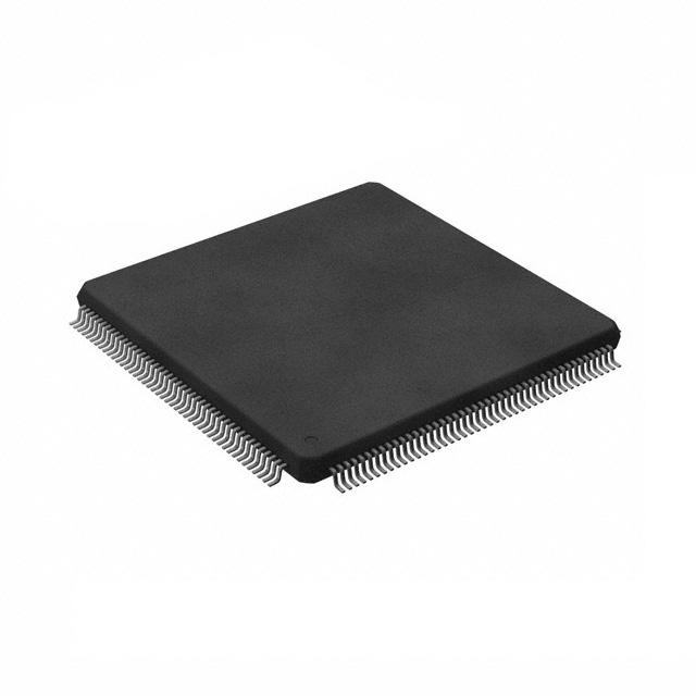
QFP-176 (series variant)
Document Number: 002-05678 Rev. *C
Page 9 of 321
�CY9EF226 - Titan
Table 3. Memory Map
Start Address
Module
Start Address
Module
FFFF4000
Reserved
05FE0000
AXI_SLAVE_CORE0_TCM_FLASH_SMALL_SECTORS
FFFF0000
BOOTROM
05A00000
Reserved
FFFEF000
ERCFG_CONFIG
05800000
AXI_SLAVE_CORE0_TCM_FLASH_LARGE_SECTORS
B0D01000
Reserved
05020000
Reserved
B0D00000
SYSTEM_RAM_CONFIG
05000000
AXI_SLAVE_CORE0_TCM_RAM
B0C00000
PERI5_AHB
04800000
AXI_SLAVE_CORE0_DCACHE
B0B00000
PERI4_SLAVE
04000000
AXI_SLAVE_CORE0_ICACHE
B0A00000
PERI3_ERBUS
01A10000
Reserved
B0900000
Reserved
01A00000
SYSTEM_RAM
B0800000
PERI1_RBUS
01800000
Reserved
B0700000
PERI0_RBUS
017E0000
AXI_FLASH_MEMORY_SMALL_SECTORS
B0600000
MCU_CONFIG
01200000
Reserved
B0500000
DEBUG_BUS
00100000
AXI_FLASH_MEMORY_LARGE_SECTORS
B0400000
MEMORY_CONFIG
00FE0000
TCM_FLASH_SMALL_SECTORS
B0180000
Reserved
00A00000
Reserved
B0100000
GFXCFG
00080000
TCM_FLASH_LARGE_SECTORS
B0080000
Reserved
00020000
Reserved
B0000000
HSSPI0CFG
00000000
TCM_RAM
90000000
Reserved
80000000
HSSPI0_MEMORY
60000000
Reserved
40000000
GFXMEM
06000000
Reserved
Table 4. HSSPI0 Memory Map
Start Address
Module
B007FC00
BSU8
B0078400
Reserved
B0078000
RICFG8
B0000000
HSSPI0
Document Number: 002-05678 Rev. *C
Table 5. Memory and Config (MEMORY_CONFIG) AHB Bus
Memory Map
Start Address
Module
B04C0000
EEFLASH_NOECC_MIR
B0480000
EEFLASH_TABLE_MIR
B0440000
EEFLASH_ECC_MIR
B0418400
Reserved
B0418000
BSU6
B0414400
Reserved
B0414000
MPUXSHE0
B0413400
Reserved
B0413000
SHE_IF_CFG
B0412400
Reserved
B0412000
EEFCFG
B0411400
Reserved
B0411000
TCFCFG
Page 10 of 321
�CY9EF226 - Titan
Table 5. Memory and Config (MEMORY_CONFIG) AHB Bus
Memory Map (Continued)
Table 7. PERI0_RBUS Memory Map (Continued)
Start Address
Module
Start Address
Module
B0748400
PPGGRP1
B0410400
Reserved
B0748000
PPGGRP0
B0410000
TRCFG
B073BC00
PPG15
B0408400
Reserved
B073B800
PPG14
B0408000
TPU0
B073B400
PPG13
B0404000
Reserved
B073B000
PPG12
B0400000
IRQ0
B073AC00
PPG11
B073A800
PPG10
B073A400
PPG9
B073A000
PPG8
B0739C00
PPG7
B0739800
PPG6
B0739400
PPG5
Table 6. MCU_CONFIG AHB Bus Memory Map
Start Address
Module
B06FFC00
BSU7
B06F8000
RICFG7
B0648000
Reserved
B063B000
RETRAMBANK3
B063A000
RETRAMBANK2
B0639000
RETRAMBANK1
B0638000
RETRAMBANK0
B0628400
Reserved
B0628000
EICU0
B0620400
Reserved
B0620000
EIC0
B0618400
Reserved
B0618000
RTC
B0610400
Reserved
B0610000
RRCFG
B0608400
Reserved
B0608000
WDG
B0601000
Reserved
B0600000
SYSC
Table 7. PERI0_RBUS Memory Map
B0739000
PPG4
B0738C00
PPG3
B0738800
PPG2
B0738400
PPG1
B0738000
PPG0
B0731C00
Reserved
B0731800
SMCTG0
B0731400
SMC5
B0731000
SMC4
B0730C00
SMC3
B0730800
SMC2
B0730400
SMC1
B0730000
SMC0
B0729800
Reserved
B0728000
USART0
B0720C00
Reserved
B0720000
I2C0
Reserved
OCU1
Start Address
Module
B071C000
B07FFC00
BSU0
B0718400
B07F8000
RICFG0
B0718000
OCU0
B07F0400
Reserved
B0714000
Reserved
B07F0000
BECU0
B0710C00
ICU3
B07EC000
Reserved
B0710800
ICU2
B07E8000
PPC
B070C000
Reserved
B074C400
Reserved
B0708C00
FRT3
B074C000
PPGGLC0
B0708800
FRT2
B0748C00
PPGGRP3
B0708400
FRT1
B0748800
PPGGRP2
B0708000
FRT0
Document Number: 002-05678 Rev. *C
Page 11 of 321
�CY9EF226 - Titan
Table 7. PERI0_RBUS Memory Map (Continued)
Start Address
Module
B0700400
Reserved
Start Address
Module
B0700000
ADC0
B0AFFC00
BSU3
Table 8. PERI1_RBUS Memory Map
Start Address
Module
B08FFC00
BSU1
B08F8000
RICFG1
B08F0400
Reserved
B08F0000
BECU1
B085C400
Reserved
B085C000
PPGGLC1
B0858400
PPGGRP17
B0858000
PPGGRP16
B0849C00
PPG71
B0849800
PPG70
B0849400
PPG69
B0849000
PPG68
B0848C00
PPG67
B0848800
PPG66
B0848400
PPG65
B0848000
PPG64
B0839800
Reserved
B0838000
USART6
B082C000
Reserved
B0828400
OCU17
B0828000
OCU16
B0824000
Reserved
B0820C00
ICU19
B0820800
ICU18
B081C000
Reserved
B0818C00
FRT19
B0818800
FRT18
B0818400
FRT17
B0818000
FRT16
B080A000
Reserved
B0808400
CAN1
B0808000
CAN0
B0801000
Reserved
B0800000
SG0
Document Number: 002-05678 Rev. *C
Table 9. PERI3_eRBUS Memory Map
B0AF8000
RICFG3
B0AF0400
Reserved
B0AF0000
BECU3
B0A21000
Reserved
B0A20000
UDC0
B0A18000
Reserved
B0A12400
RLT9
B0A12000
RLT8
B0A11C00
RLT7
B0A11800
RLT6
B0A11400
RLT5
B0A11000
RLT4
B0A10C00
RLT3
B0A10800
RLT2
B0A10400
RLT1
B0A10000
RLT0
B0A09000
Reserved
B0A08000
GPIO
B0A00400
Reserved
B0A00000
PPU0
Table 10. PERI4_SLAVE AHB Bus Memory Map
Start Address
Module
B0BFFC00
BSU4
B0BF8000
RICFG4
B0B40400
Reserved
B0B40000
ARH0
B0B3B000
Reserved
B0B38800
SPI2
B0B38400
SPI1
B0B38000
SPI0
B0B30800
Reserved
B0B30000
CRC0
B0B22000
Reserved
B0B20400
I2S1
B0B20000
I2S0
B0B10800
Reserved
B0B10400
MPUHMLB0
Page 12 of 321
�CY9EF226 - Titan
Table 10. PERI4_SLAVE AHB Bus Memory Map (Continued)
Start Address
Lock/Unlock Values for Protection Units
For various protection and system relevant units, registers must
be unlocked before configuring and can be locked for protection.
For the details about functionality, see the FCR4 Hardware
Manual.
Module
B0B10000
MLB0
B0B00400
Reserved
B0B00000
MPUXGFX
Table 13. Lock/Unlock Values for FCR4 Protection Module
Instances
Module
Table 11. PERI5_AHB Bus Memory Map
Unlock Value
Lock Value
TPU0
ACC5A110
B10CACC5
ACC5BB01
BB0B10C1
D76B10C1
Start Address
Module
PPU0
B0CFFC00
BSU5
MPUHMLB0
D76ACC01
B0C09000
Reserved
MPUXDMA0
ACCABB56
112ABB56
B0C08000
MPUXDMA0
MPUXGFX
01ACC384
0B10C834
B0C04000
Reserved
MPUXSHE0
0x15EDDE51
10CE0EB1
B0C00000
DMA0
TRCFG
ACC55ECC
5ECCB10C
B0800000
PERI1_RBUS
EXCFG
ACC5B007
B007ECF6
B0700000
PERI0_RBUS
Resource Distribution for Non-modulated Clock
Some of the resources are available with modulated and
non-modulated clock. Table 12 provides the distribution.
Table 12. Clock Modulation for Resources
Module
Non-modulated
IRQ0
17ACC911
17B10C11
RRCFG
ACC5DECC
DECCB10C
SCCFG
5ECACCE5
A135331A
SRCFG
5ECC551F
551FB10C
GFXSIG
A1ACC384
AB10C834
GFXGCTR
7E1ECA57
D15AB1E0
Modulation
Possible
TCFCFG
CF61F1A5
EEFCFG
CF6DF1A5
CAN
2
-
SG
1
-
WDG
EDACCE55
SYSC
5CACCE55
ICU/OCU/FRT
4
4
PPG
8
16
USART/LIN
1
1
I2C
1
-
SMC
-
6
Document Number: 002-05678 Rev. *C
Page 13 of 321
�CY9EF226 - Titan
ID-Values for Module Identification Registers
For several peripheral and system related modules, the hardware contains Module Identification Registers that hold read-only values
which contain information about the module number, the version and possible patches.
Table 14. Module ID List
Module
ID-Register
ID Value
System Controller
SYSC_SYSIDR
0x00041100
Security Checker
SCCFG_MODID
0x00020400
SRAM Interface
SRCFG_MID
0x00040300
TC-Flash Interface
TCFCFG_FMIDR
0x000E0400
EE-Flash Interface
EEFCFG_MIR
0x00090700
Interrupt Controller 0
IRQ0_MID
0x000B0100
DMA Controller 0
DMA0_ID
0x00010400
Timing Protection Unit 0
TPU0_MID
0x00050200
Memory Protection Unit for DMA
MPUXDMA0_MID
0x000D0200
Memory Protection Unit for GFX
MPUXGFX_MID
0x000D0200
Memory Protection Unit for SHE
MPUXSHE0_MID
0x000D0200
Memory Protection Unit for MLB
MPUHMLB0_MID
Bus Error Collection Unit 0
BECU0_MIDH / BECU0_MIDL
0x0008 / 0x0300
Bus Error Collection Unit 1
BECU1_MIDH / BECU1_MIDL
0x0008 / 0x0300
Bus Error Collection Unit 3
BECU3_MIDH / BECU3_MIDL
0x0008 / 0x0300
High Speed SPI Interface 0
HSSPI0_MID
0x00060400
SPI Interface 0
SPI0_MID
0x00070400
SPI Interface 1
SPI1_MID
0x00070400
SPI Interface 2
SPI2_MID
0x00070400
Inter IC Sound 0
I2S0_MIDREG
0x000A0300
Inter IC Sound 1
I2S1_MIDREG
0x000A0300
SHE
SHE_IF_CFG_MID
0x000F0200
Document Number: 002-05678 Rev. *C
0x00110100
Page 14 of 321
�CY9EF226 - Titan
Package and Pin Assignment
Package
QFP-176 package will be used for CY9EF226. The package code is LQP176.
QFP-176 Pin Assignment
P1_00
DVCC
DVSS
VSS
VDP3
VDD
P1_47
P1_46
P1_45
P1_44
P1_43
99
98
97
96
95
94
93
92
91
90
89
100 P1_01
101 P1_02
102 P1_03
103 P1_04
104 P1_05
105 P1_06
106 P1_07
107 DVSS
108 DVCC
109 P1_08
110 P1_09
111 P1_10
112 P1_11
113 P1_12
114 P1_13
115 P1_14
116 P1_15
117 DVSS
118 DVCC
119 P1_16
120 P1_17
121 P1_18
122 P1_19
123 P1_20
124 P1_21
125 P1_22
126 P1_23
127 DVSS
128 DVCC
129 AVSS5
130 AVRH5
131 AVDD5
132 VDP5
Figure 1. QFP-176 Pin Assignment
VSS
133
88
P1 42
P0 24
134
87
P1 41
P0 25
135
86
P1 40
P0 40
136
85
P1 39
P0 41
137
84
P1 29
VSS
138
83
P1 28
VDD
139
82
P1 27
P0 42
140
81
P1 26
P0 43
141
80
VSS
P0 44
142
79
VDP3
P0 45
143
78
P1 59
P0 46
144
77
P1 58
P0 47
145
76
P1 57
VSS
146
75
P1 56
VDP5
147
74
P1 55
P0 48
148
73
P1 54
P0 49
149
72
VSS
P2 32
150
71
VDP3
P2 33
151
70
P1 53
P2 34
152
69
P1 52
P2 35
153
68
P1 51
P2 36
154
67
P1 50
P2 37
155
66
P1 49
VSS
156
65
P1 48
VSS
VDD
157
64
P2 38
158
63
VDP3
P2 39
159
62
P2 25
P2 40
160
61
P2 24
P2 41
161
60
VSS
P2 42
162
59
P2 23
P2 43
163
58
P2 22
P2 48
164
57
P2 49
165
56
P2 21
VSS
166
55
P2 20
`
`
`
`
VDD
VDP5
167
54
VDP3
P2 50
168
53
P2 19
P2 51
169
52
P2 18
P0 62
170
51
VSS
P0 63
171
50
P2 17
JTAG TDO
172
49
P2 16
JTAG TDI
173
48
VDP3
JTAG TMS
174
47
P2 15
3
4
5
6
7
8
9
10
11
12
13
14
15
16
17
18
19
20
21
22
23
24
25
26
27
28
29
30
31
32
33
34
35
36
37
38
39
40
41
42
43
44
X0
VSS
X0A
X1A
RSTX
VDP5
VSS
VDP3
P1_30
P1_31
P1_32
P1_33
P1_34
P1_35
P1_36
P1_37
P1_38
P1_61
P1_62
P1_60
VSS
VDP3
P2_00
P2_01
VSS
P2_02
P2_03
VDD
P2_04
P2_05
VDP3
P2_06
P2_07
VSS
P2_08
P2_09
VDP3
P2_10
P2_11
VSS
P2_12
P2_13
VDD
2
P2 14
1
46
45
X1
175
176
MODE
JTAG TCK
TAG NTRST
Document Number: 002-05678 Rev. *C
Page 15 of 321
�CY9EF226 - Titan
Table 15. QFP-176 Package Pinout
Pin Number
Pin Name
Pin Number
Pin Name
1
2
MODE
40
P2_10
X1
41
P2_11
3
X0
42
VSS
4
VSS
43
P2_12
5
X0A
44
P2_13
6
X1A
45
VDD
7
RSTX
46
P2_14
8
VDP5
47
P2_15
9
VSS
48
VDP3
10
VDP3
49
P2_16
11
P1_30
50
P2_17
12
P1_31
51
VSS
13
P1_32
52
P2_18
14
P1_33
53
P2_19
15
P1_34
54
VDP3
16
P1_35
55
P2_20
17
P1_36
56
P2_21
18
P1_37
57
VDD
19
P1_38
58
P2_22
20
P1_61
59
P2_23
21
P1_62
60
VSS
22
P1_60
61
P2_24
23
VSS
62
P2_25
24
VDP3
63
VDP3
25
P2_00
64
VSS
26
P2_01
65
P1_48
27
VSS
66
P1_49
28
P2_02
67
P1_50
29
P2_03
68
P1_51
30
VDD
69
P1_52
31
P2_04
70
P1_53
32
P2_05
71
VDP3
33
VDP3
72
VSS
34
P2_06
73
P1_54
35
P2_07
74
P1_55
36
VSS
75
P1_56
37
P2_08
76
P1_57
38
P2_09
77
P1_58
39
VDP3
78
P1_59
79
VDP3
118
DVCC
80
VSS
119
P1_16
Document Number: 002-05678 Rev. *C
Page 16 of 321
�CY9EF226 - Titan
Table 15. QFP-176 Package Pinout (Continued)
Pin Number
Pin Name
Pin Number
Pin Name
81
P1_26
120
P1_17
82
P1_27
121
P1_18
83
P1_28
122
P1_19
84
P1_29
123
P1_20
85
P1_39
124
P1_21
86
P1_40
125
P1_22
87
P1_41
126
P1_23
88
P1_42
127
DVSS
89
P1_43
128
DVCC
90
P1_44
129
AVSS5
91
P1_45
130
AVRH5
92
P1_46
131
AVDD5
93
P1_47
132
VDP5
94
VDD
133
VSS
95
VDP3
134
P0_24
96
VSS
135
P0_25
97
DVSS
136
P0_40
98
DVCC
137
P0_41
99
P1_00
138
VSS
100
P1_01
139
VDD
101
P1_02
140
P0_42
102
P1_03
141
P0_43
103
P1_04
142
P0_44
104
P1_05
143
P0_45
105
P1_06
144
P0_46
106
P1_07
145
P0_47
107
DVSS
146
VSS
108
DVCC
147
VDP5
109
P1_08
148
P0_48
110
P1_09
149
P0_49
111
P1_10
150
P2_32
112
P1_11
151
P2_33
113
P1_12
152
P2_34
114
P1_13
153
P2_35
115
P1_14
154
P2_36
116
P1_15
155
P2_37
117
DVSS
156
VSS
157
VDD
173
JTAG_TDI
158
P2_38
174
JTAG_TMS
159
P2_39
175
JTAG_TCK
160
P2_40
176
JTAG_NTRST
Document Number: 002-05678 Rev. *C
Page 17 of 321
�CY9EF226 - Titan
Table 15. QFP-176 Package Pinout (Continued)
Pin Number
Pin Name
Pin Number
Pin Name
161
P2_41
167
VDP5
162
P2_42
168
P2_50
163
P2_43
169
P2_51
164
P2_48
170
P0_62
165
P2_49
171
P0_63
166
VSS
172
JTAG_TDO
Document Number: 002-05678 Rev. *C
Page 18 of 321
�CY9EF226 - Titan
I/O Pins and Functions
IO Pin configuration needs to be done by writing into Port Pin Multiplexing registers and Resource Input Configuration registers which
are described in Port Pin Multiplexing and Resource Input Source. GPIO_PPERn register must be enabled before starting IO Pin
configuration, since GPIO_PPERn enables corresponding pin of the device.
Note Since writing GPIO PPERn registers are required for both Portmux & resource-mux registers.
Port Pin Multiplexing
Table 16. Port Multiplexing
Register
(Offset)
Resource Functional Output
Port
PCFGR024
P0_24
(0x0030)
PCFGR025
P0_25
(0x0032)
PCFGR040
P0_40
(0x0050)
POF=0
POF=1
POF=2
POF=3
GPIO0_24o
OCU0_OTD0
_GI
GPIO0_25o
OCU0_OTD1
CAN1_TX
_GI
GPIO0_40o SPI2_SSo
POF=4
PPG8_PPGB
RTC_WOT
PPG9_PPGB
POF=5
OCU0_OTD0
OCU0_OTD1
PPG64_PPGB OCU16_OTD0_G
POF=6
POF=7
Possible
Resource
Function Input
RLT3_TOT PPG0_PPGA
GPIO0_24i,
EIC0_INT09,
EIC0_INT10,
CAN1_RX, ICU2_IN0
RLT4_TOT PPG1_PPGA
GPIO0_25i,
EIC0_INT08,
CAN0_RX,
ICU2_IN1,
ADC0_AN25
PPG8_PPGA
GPIO0_40i,
EIC0_INT05,
EIC0_INT12,
EIC0_INT11,
SPI2_SSi,
USART6_SIN,
USART0_SIN,
FRT0_FRCK,
RLT5_TIN,
ADC0_AN15
PPG9_PPGA
GPIO0_41i,
EIC0_INT15, SPI2_DATA1i,
USART6_SCKi,
USART0_SCKi,
FRT1_FRCK,
RLT6_TIN,
ICU2_IN0,
ICU18_IN1,
ADC0_AN16
PCFGR041 P0_41
(0x0052)
GPIO0_41o SPI2_DATA1o SYSC_CKOT USART6_S PPG65_PPGB OCU16_OTD1_G
CKo
PCFGR042 P0_42
(0x0054)
GPIO0_42i,
EIC0_INT08,
EIC0_INT10,
EIC0_INT11, SPI2_DATA0i, CAN0_RX,
GPIO0_42o SPI2_DATA0o SYSC_CKOT USART6_S PPG66_PPGB OCU17_OTD0_G RLT2_TOT PPG10_PPGA FRT2_FRCK,
X
OT
CAN1_RX,
ICU2_IN1,
ICU19_IN0,
USART0_SIN,
ADC0_AN17
PCFGR043
P0_43
(0x0056)
PCFGR044 P0_44
(0x0058)
GPIO0_43o SPI2_CLKo
GPIO0_44o SPI0_SSo
Document Number: 002-05678 Rev. *C
WDG_OBSERVE
CAN0_TX
SPI2_SSO2
SPI2_DATA2o
PPG67_PPGB OCU17_OTD1_G
PPG68_PPGB OCU0_OTD0_G
PPG11_PPGA
GPIO0_43i,
EIC0_INT09,
SPI2_CLKi,
CAN1_RX,
FRT3_FRCK,
RLT2_TIN,
ADC0_AN18
GPIO0_44i,
EIC0_INT03, SPI2_SPI0_Ssi,
RLT3_TOT PPG12_PPGA DATA2i,
FRT16_FRCK,
UDC0_AIN0,
ADC0_AN19
Page 19 of 321
�CY9EF226 - Titan
Table 16. Port Multiplexing (Continued)
Register
(Offset)
Resource Functional Output
Port
PCFGR045
P0_45
(0x005A)
PCFGR046 P0_46
(0x005C)
PCFGR047 P0_47
(0x005E)
PCFGR048
P0_48
(0x0060)
POF=0
POF=1
POF=2
GPIO0_45o SPI0_DATA1o SPI2_SSO3
GPIO0_46o SPI0_DATA0o SPI2_SSO1
GPIO0_47o SPI0_CLKo
GPIO0_48o SPI1_SSo
UDC0_UDO
T0
SPI0_SSO2
POF=3
SPI2_DATA3o
POF=4
POF=5
PPG69_PPGB OCU0_OTD1_G
USART0_S PPG70_PPGB OCU1_OTD0_G
CKo
POF=6
POF=7
Possible
Resource
Function Input
GPIO0_45i,
EIC0_INT11,
EIC0_INT12,
FRT16_FRCK,
FRT18_FRCK,
SPI2_DATA3i, SPI0_DATA1i,
PPG13_PPGA
USART0_SIN,
USART6_SIN,
FRT17_FRCK,
RLT3_TIN,
FRT19_FRCK,
UDC0_BIN0,
ADC0_AN20
GPIO0_46i,
EIC0_INT16, SPI0_DATA0i,
USART0_SCKi,
USART6_SCKi,
PPG14_PPGA
FRT18_FRCK,
RLT4_TIN,
UDC0_ZIN0,
ICU18_IN0,
ADC0_AN21
USART0_S PPG71_PPGB OCU1_OTD1_G
OT
GPIO0_47i,
FRT0_FRCK,
FRT1_FRCK,
FRT2_FRCK,
EIC0_INT17,
FRT3_FRCK,
SPI0_CLKi,
OCU16_O PPG15_PPGA FRT16_FRCK,
FRT17_FRCK,
TD0_GI
FRT19_FRCK,
RLT0_TIN,
FRT18_FRCK,
EIC0_INT12,
ICU18_IN1,
USART6_SIN,
ADC0_AN22
SPI0_DATA2o
OCU0_OTD0
GPIO0_48i,
EIC0_INT04,
EIC0_INT09,
EIC0_INT08, SPI0_DATA2i, SPI1_Ssi,
RLT4_TOT PPG64_PPGA CAN1_RX,
CAN0_RX,
ICU2_IN0,
UDC0_AIN1,
ADC0_AN23
OCU0_OTD1
GPIO0_49i,
EIC0_INT10, SPI1_RLT0_TOT PPG65_PPGA DATA1i, ICU2_IN1,
CAN0_RX,
UDC0_BIN1,
ADC0_AN24
PPG0_PPGB
PCFGR049 P0_49
(0x0062)
GPIO0_49o SPI1_DATA1o SPI0_SSO1
PCFGR062 P0_62
(0x007C)
GPIO0_62o I2C0_SCLo
GPIO0_62i,
EIC0_INT24,
I2C0_SCLi
PCFGR063 P0_63
(0x007E)
GPIO0_63o I2C0_SDAo
GPIO0_63i,
EIC0_INT00,
I2C0_SDAi
PCFGR100 P1_00
(0x0080)
GPIO1_00o SMC0_M2
PPG64_PPGB
PPG0_PPGA
GPIO1_00i,
CAN0_RX,
EIC0_INT08,
EIC0_INT25,
ADC0_AN26
PCFGR101
P1_01
(0x0082)
GPIO1_01o SMC0_P2
PPG65_PPGB CAN0_TX
PPG1_PPGA
GPIO1_01i,
EIC0_INT26,
ADC0_AN26
PPG2_PPGA
GPIO1_02i,
EIC0_INT13,
CAN1_RX,
EIC0_INT09,
ADC0_AN26
PCFGR102
P1_02
(0x0084)
GPIO1_02o SMC0_M1
Document Number: 002-05678 Rev. *C
CAN1_TX
PPG1_PPGB
PPG66_PPGB
Page 20 of 321
�CY9EF226 - Titan
Table 16. Port Multiplexing (Continued)
Register
(Offset)
Resource Functional Output
Port
POF=0
POF=1
POF=2
POF=3
POF=4
POF=5
POF=6
POF=7
Possible
Resource
Function Input
PCFGR103
P1_03
(0x0086)
GPIO1_03o SMC0_P1
PPG67_PPGB CAN1_TX
PPG3_PPGA
GPIO1_03i,
EIC0_INT27,
ADC0_AN26
PCFGR104
P1_04
(0x0088)
GPIO1_04o SMC1_M2
PPG68_PPGB
PPG4_PPGA
GPIO1_04i,
EIC0_INT28,
ADC0_AN27
PCFGR105
P1_05
(0x008A)
GPIO1_05o SMC1_P2
PPG69_PPGB
PPG5_PPGA
GPIO1_05i,
EIC0_INT29,
ADC0_AN27
PCFGR106
P1_06
(0x008C)
GPIO1_06o SMC1_M1
PPG70_PPGB
PPG6_PPGA
GPIO1_06i,
EIC0_INT30,
ADC0_AN27
PCFGR107
P1_07
(0x008E)
GPIO1_07o SMC1_P1
PPG71_PPGB
PPG7_PPGA
GPIO1_07i,
EIC0_INT31,
ADC0_AN27
PPG8_PPGA
GPIO1_08i,
USART0_SIN,
RLT3_TIN,
EIC0_INT00,
SPI0_SSi,
ADC0_AN28,
EIC0_INT03,
EIC0_INT11
GPIO1_09i,
USART0_SCKi,
RLT4_TIN,
EIC0_INT01, SPI0_DATA1i, ICU2_IN1,
ADC0_AN28
PCFGR108 P1_08
(0x0090)
GPIO1_08o SMC2_M2
PPG0_PPGB
SPI0_SSo
PCFGR109 P1_09
(0x0092)
GPIO1_09o SMC2_P2
PPG1_PPGB
SPI0_DATA1o
USART0_
SCKo
PPG9_PPGA
PCFGR110 P1_10
(0x0094)
GPIO1_10o SMC2_M1
PPG2_PPGB
SPI0_DATA0o
USART0_
SOT
GPIO1_10i,
PPG10_PPGA EIC0_INT02, SPI0_DATA0i, ICU2_IN0,
ADC0_AN28
PCFGR111 P1_11
(0x0096)
GPIO1_11o SMC2_P1
PPG3_PPGB
SPI0_CLKo
PPG11_PPGA
SPI1_SSo
GPIO1_12i,
USART6_SIN,
RLT5_TIN,
PPG12_PPGA EIC0_INT04,
SPI1_SSi,
ADC0_AN29,
EIC0_INT12
PCFGR112 P1_12
(0x0098)
GPIO1_12o SMC3_M2
PPG4_PPGB
PCFGR113 P1_13
(0x009A)
GPIO1_13o SMC3_P2
PPG5_PPGB
PCFGR114 P1_14
(0x009C)
GPIO1_14o SMC3_M1
PPG6_PPGB
PCFGR115 P1_15
(0x009E)
GPIO1_15o SMC3_P1
PPG7_PPGB
GPIO1_11i,
EIC0_INT03,
SPI0_CLKi,
RLT0_TIN,
ADC0_AN28
SPI1_DATA1o
USART6_
SCKo
GPIO1_13i,
USART6_SCKi,
PPG13_PPGA RLT6_TIN,
EIC0_INT05, SPI1_DATA1i, ICU18_IN0,
ADC0_AN29
SPI1_DATA0o
USART6_
SOT
GPIO1_14i,
PPG14_PPGA EIC0_INT06, SPI1_DATA0i, ICU19_IN1,
ADC0_AN29
SPI1_CLKo
GPIO1_15i,
EIC0_INT07,
PPG15_PPGA SPI1_CLKi,
RLT1_TIN,
ADC0_AN29
PCFGR116 P1_16
(0x00A0)
GPIO1_16o SMC4_M2
PPG8_PPGB
SPI2_SSo
GPIO1_16i,
EIC0_INT10,
SPI1_SSO PPG64_PPGA EIC0_INT13,
2
SPI2_SSi,
ADC0_AN30,
EIC0_INT05
PCFGR117 P1_17
(0x00A2)
GPIO1_17o SMC4_P2
PPG9_PPGB
SPI2_DATA1o
GPIO1_17i,
SPI1_SSO PPG65_PPGA EIC0_INT14, SPI2_1
DATA1i, ADC0_AN30
Document Number: 002-05678 Rev. *C
Page 21 of 321
�CY9EF226 - Titan
Table 16. Port Multiplexing (Continued)
Register
(Offset)
Resource Functional Output
Port
PCFGR118
P1_18
(0x00A4)
POF=0
POF=3
POF=4
POF=5
POF=1
POF=2
GPIO1_18o SMC4_M1
SG0_SGA
DMA0_DR
EQ_ACK1
SG0_SGO
DMA0_DPPG11_PPGB SPI2_CLKo
STP_ACK1
GPIO1_19i,
EIC0_INT16,
SPI2_CLKi,
PPG67_PPGA
ICU19_IN1,
RLT2_TIN,
ADC0_AN30
DMA0_DE
OP1
PPG12_PPGB
GPIO1_20i,
PPG68_PPGA EIC0_INT17,
ADC0_AN31
PPG10_PPGB SPI2_DATA0o
POF=6
POF=7
Possible
Resource
Function Input
GPIO1_18i,
SPI1_SSO
EIC0_INT15, SPI2_PPG66_PPGA
3
DATA0i, ICU18_IN0,
ADC0_AN30
PCFGR119
P1_19
(0x00A6)
GPIO1_19o SMC4_P1
PCFGR120
P1_20
(0x00A8)
GPIO1_20o SMC5_M2
PCFGR121
P1_21
(0x00AA)
GPIO1_21o SMC5_P2
PPG13_PPGB
GPIO1_21i,
EIC0_INT18,
PPG69_PPGA DMA0_DREQ1,
ADC0_AN31
PCFGR122 P1_22
(0x00AC)
GPIO1_22o SMC5_M1
PPG14_PPGB
GPIO1_22i,
PPG70_PPGA EIC0_INT19,
DMA0_DSTP1,
ADC0_AN31
PPG15_PPGB
GPIO1_23i,
EIC0_INT20,
PPG71_PPGA DMA0_DEOP_ACK1,
ADC0_AN31
PCFGR123 P1_23
(0x00AE)
GPIO1_23o SMC5_P1
PCFGR126 P1_26
(0x00B4)
GPIO1_26o DBG0_TRAC
E0
PCFGR127 P1_27
(0x00B6)
GPIO1_27o DBG0_TRAC
E1
PCFGR128 P1_28
(0x00B8)
GPIO1_28o DBG0_CTL
RLT3_TOT
GPIO1_28i,
EIC0_INT22,
DMA0_DSTP0
PCFGR129 P1_29
(0x00BA)
GPIO1_29o DBG0_CLK
RLT4_TOT
GPIO1_29i,
EIC0_INT23,
DMA0_DEOP_ACK0
DMA0_DEO
P0
I2S1_WSo
PPG7_PPGB
GPIO1_26i,
PPG71_PPGA EIC0_INT07,
I2S1_Wsi,
ICU19_IN1
OCU17_OTD1
GPIO1_27i,
EIC0_INT21,
DMA0_DREQ0,
I2S1_SCKi
I2S1_SCKo
PCFGR130 P1_30
(0x00BC)
GPIO1_30o HSSPI0_SSO OCU0_OTD0
3
PCFGR131
P1_31
(0x00BE)
HSSPI0_SSO
USART0_S DBG0_TRACE DMA0_DSTGPIO1_31o 2
OCU0_OTD1 CKo
3
P_ACK0
GPIO1_31i,
EIC0_INT24,
USART0_SCKi,
ICU3_IN1, RLT4_TIN
PCFGR132 P1_32
(0x00C0)
DBG0_TRACE
GPIO1_32o HSSPI0_SSO
OCU1_OTD0 USART0_S
1
OT
4
GPIO1_32i,
EIC0_INT25,
ICU3_IN0
PCFGR133 P1_33
(0x00C2)
GPIO1_33o HSSPI0_SSo
DBG0_TRACE
5
GPIO1_33i,
EIC0_INT01,
HSSPI0_SSi
PCFGR134
P1_34
(0x00C4)
HSSPI0_GPIO1_34o DATA3o
GPIO1_34i,
EIC0_INT08,
HSSPI0_DATA3i,
CAN0_RX,
UDC0_AIN0
PCFGR135 P1_35
(0x00C6)
GPIO1_35o HSSPI0_DATA2o
GPIO1_35i,
EIC0_INT26,
HSSPI0_DATA2i,
ICU2_IN0,
UDC0_BIN0
Document Number: 002-05678 Rev. *C
DBG0_TRACE DMA0_DREQ_A
2
CK0
GPIO1_30i,
EIC0_INT11,
PPG_ETRG2,
GFX0_DCLKI,
USART0_SIN,
RLT3_TIN,
ADC0_EDGI
OCU1_OTD1 CAN0_TX
CAN1_TX
Page 22 of 321
�CY9EF226 - Titan
Table 16. Port Multiplexing (Continued)
Register
(Offset)
Resource Functional Output
Port
POF=0
POF=1
POF=2
POF=3
POF=4
POF=5
POF=6
POF=7
Possible
Resource
Function Input
GPIO1_36i,
EIC0_INT09,
HSSPI0_DATA1i,
CAN1_RX,
ICU2_IN1,
UDC0_ZIN0
PCFGR136
P1_36
(0x00C8)
GPIO1_36o
HSSPI0_DATA1o
PCFGR137
P1_37
(0x00CA)
GPIO1_37o
HSSPI0_DATA0o
PCFGR138
P1_38
(0x00CC)
GPIO1_38o HSSPI0_CLKo
PCFGR139
P1_39
(0x00CE)
GFXSPI_SSO OCU16_OTD
GPIO1_39o 3
0
GPIO1_39i,
EIC0_INT12,
GFX0_DCLKI,
USART6_SIN,
RLT5_TIN
PCFGR140
P1_40
(0x00D0)
GFXSPI_SSO OCU16_OTD USART6_S DBG0_TRACE
GPIO1_40o 2
1
CKo
6
GPIO1_40i,
EIC0_INT27,
PPG_ETRG3,
USART6_SCKi,
RLT6_TIN,
ADC0_EDGI,
ICU2_IN0
PCFGR141 P1_41
(0x00D2)
OCU17_OTD USART6_S DBG0_TRACE
GPIO1_41o GFXSPI_SSO
1
0
OT
7
PCFGR142 P1_42
(0x00D4)
GPIO1_42o GFXSPI_SSo
PCFGR143 P1_43
(0x00D6)
UDC0_UDO
T0
OCU17_OTD
1
GPIO1_43o GFXSPI_DATA3o
PPG70_PPGB
PPG71_PPGB
PCFGR144 P1_44
(0x00D8)
GPIO1_44o GFXSPI_DATA2o
USART0_S PPG0_PPGB
CKo
PCFGR145 P1_45
(0x00DA)
GPIO1_45o GFXSPI_DATA1o
USART0_S PPG1_PPGB
OT
PCFGR146 P1_46
(0x00DC)
GPIO1_46o GFXSPI_DATA0o
PCFGR147
P1_47
(0x00DE)
RLT5_TOT
GPIO1_37i,
EIC0_INT13,
HSSPI0_DATA0i,
ICU3_IN0
RLT6_TOT
GPIO1_38i,
EIC0_INT10,
HSSPI0_CLKi,
ICU3_IN1/
RLT3_TOT
GPIO1_41i,
EIC0_INT28,
ICU2_IN1
RLT4_TOT PPG6_PPGA
GPIO1_42i,
EIC0_INT02,
GFXSPI_SSi
PPG7_PPGA
GPIO1_43i,
EIC0_INT11,
GFXSPI_DATA3i,
USART0_SIN,
ICU18_IN0,
RLT3_TIN,
UDC0_AIN1
PPG8_PPGA
GPIO1_44i,
EIC0_INT29,
GFXSPI_DATA2i,
USART0_SCKi,
ICU18_IN1,
RLT4_TIN,
UDC0_BIN1
PPG9_PPGA
GPIO1_45i,
EIC0_INT30,
GFXSPI_DATA1i,
ICU19_IN0,
UDC0_ZIN1
PPG2_PPGB
GPIO1_46i,
PPG10_PPGA EIC0_INT31,
GFXSPI_DATA0i,
ICU19_IN1
GFXSPI_CLK
GPIO1_47o o
PPG3_PPGB
PPG11_PPGA
PCFGR148 P1_48
(0x00E0)
GPIO1_48o GFX0_TSIG0
PPG4_PPGB
PPG12_PPGA GPIO1_48i,
EIC0_INT01
PCFGR149
P1_49
(0x00E2)
GPIO1_49o GFX0_TSIG1
PPG5_PPGB
GPIO1_49i,
PPG13_PPGA EIC0_INT02
PCFGR150 P1_50
(0x00E4)
GPIO1_50o GFX0_TSIG2
PPG6_PPGB
PPG14_PPGA GPIO1_50i,
EIC0_INT14
PCFGR151 P1_51
(0x00E6)
GPIO1_51o GFX0_TSIG3
PPG7_PPGB
PPG15_PPGA GPIO1_51i,
EIC0_INT15
PCFGR152 P1_52
(0x00E8)
GPIO1_52o GFX0_TSIG4
PPG8_PPGB
GPIO1_52i,
PPG64_PPGA EIC0_INT16,
ICU2_IN0
Document Number: 002-05678 Rev. *C
UDC0_UDO
T1
UDC0_UDO
T0
GPIO1_47i,
EIC0_INT00,
GFXSPI_CLKi
Page 23 of 321
�CY9EF226 - Titan
Table 16. Port Multiplexing (Continued)
Register
(Offset)
Resource Functional Output
Port
POF=0
POF=1
POF=2
POF=3
POF=4
POF=5
POF=6
POF=7
Possible
Resource
Function Input
PCFGR153
P1_53
(0x00EA)
GPIO1_53o GFX0_TSIG5
PPG9_PPGB
PPG65_PPGA
GPIO1_53i,
EIC0_INT17,
ICU2_IN1,
UDC0_AIN0
PCFGR154
P1_54
(0x00EC)
GPIO1_54o GFX0_TSIG6
PPG10_PPGB
PPG66_PPGA
GPIO1_54i,
EIC0_INT18,
ICU3_IN0,
UDC0_BIN0
PCFGR155
P1_55
(0x00EE)
GPIO1_55o GFX0_TSIG7
PPG11_PPGB
PPG67_PPGA
GPIO1_55i,
EIC0_INT19,
ICU3_IN1,
UDC0_ZIN0
PCFGR156
P1_56
(0x00F0)
GPIO1_56o GFX0_TSIG8
PPG12_PPGB
GPIO1_56i,
PPG68_PPGA EIC0_INT20,
ICU18_IN0
PCFGR157 P1_57
(0x00F2)
GPIO1_57o GFX0_TSIG9
PPG13_PPGB
GPIO1_57i,
PPG69_PPGA EIC0_INT21,
ICU18_IN1,
UDC0_AIN1
PCFGR158
P1_58
(0x00F4)
GPIO1_58o GFX0_TSIG10
PPG14_PPGB
GPIO1_58i,
EIC0_INT22,
PPG70_PPGA ICU19_IN0,
UDC0_BIN1
PCFGR159 P1_59
(0x00F6)
GPIO1_59o GFX0_TSIG11
PPG15_PPGB
GPIO1_59i,
PPG71_PPGA EIC0_INT23,
ICU19_IN1,
UDC0_ZIN1
PCFGR160
P1_60
(0x00F8)
OCU17_OTD OCU17_OT
OCU17_OTD1_G
GPIO1_60o OCU17_OTD1 1_G
PPG70_PPGB I
RLT4_TOT PPG6_PPGA
D1_I
GPIO1_60i,
MLB0_CLKi,
EIC0_INT00
PCFGR161
P1_61
(0x00FA
GPIO1_61o MLB0_SIGo
GPIO1_61i,
MLB0_SIGi,
EIC0_INT01
PCFGR162
P1_62
(0x00FC)
GPIO1_62o MLB0_DATo
GPIO1_62i,
MLB0_DATi,
EIC0_INT02
PCFGR200 P2_00
(0x0100)
GPIO2_00o GFX0_DISP0
PPG64_PPGB
PPG0_PPGA
GPIO2_00i,
EIC0_INT21
PCFGR201
P2_01
(0x0102)
GPIO2_01o GFX0_DISP1
PPG65_PPGB
PPG1_PPGA
GPIO2_01i,
EIC0_INT22
PCFGR202
P2_02
(0x0104)
GPIO2_02o GFX0_DISP2
PPG66_PPGB
PPG2_PPGA
GPIO2_02i,
EIC0_INT23,
FRT0_FRCK
PCFGR203
P2_03
(0x0106)
GPIO2_03o GFX0_DISP3
PPG67_PPGB
PPG3_PPGA
GPIO2_03i,
EIC0_INT24,
FRT1_FRCK
PCFGR204 P2_04
(0x0108)
GPIO2_04o GFX0_DISP4
PPG68_PPGB
PPG4_PPGA
GPIO2_04i,
EIC0_INT25,
FRT2_FRCK,
ICU2_IN0
PCFGR205
P2_05
(0x010A)
GPIO2_05o GFX0_DISP5
PPG69_PPGB
PPG5_PPGA
GPIO2_05i,
EIC0_INT26,
FRT3_FRCK,
ICU2_IN1
PCFGR206 P2_06
(0x010C)
GPIO2_06o GFX0_DISP6
PPG70_PPGB
PPG6_PPGA
GPIO2_06i,
EIC0_INT27,
FRT16_FRCK,
ICU3_IN0
PCFGR207 P2_07
(0x010E)
GPIO2_07o GFX0_DISP7
PPG71_PPGB
PPG7_PPGA
GPIO2_07i,
EIC0_INT28,
FRT17_FRCK,
ICU3_IN1
PCFGR208
P2_08
(0x0110)
GPIO2_08o GFX0_DISP8
PPG0_PPGB
PPG8_PPGA
GPIO2_08i,
EIC0_INT29,
FRT18_FRCK,
ICU18_IN0
Document Number: 002-05678 Rev. *C
UDC0_UDO
T1
OCU0_OTD0
Page 24 of 321
�CY9EF226 - Titan
Table 16. Port Multiplexing (Continued)
Register
(Offset)
Resource Functional Output
Port
POF=0
POF=1
POF=2
POF=3
POF=4
POF=5
POF=6
POF=7
Possible
Resource
Function Input
PCFGR209
P2_09
(0x0112)
GPIO2_09o GFX0_DISP9
PPG1_PPGB
OCU0_OTD1
PPG9_PPGA
GPIO2_09i,
EIC0_INT30,
FRT19_FRCK,
ICU18_IN1
PCFGR210
P2_10
(0x0114)
GPIO2_10o GFX0_DISP10
PPG2_PPGB
OCU1_OTD0
PPG10_PPGA
GPIO2_10i
EIC0_INT31
FRT0_FRCK
ICU19_IN0
PCFGR211
P2_11
(0x0116)
GPIO2_11o GFX0_DISP11
PPG3_PPGB
OCU1_OTD1
PPG11_PPGA
GPIO2_11i,
EIC0_INT14,
FRT1_FRCK,
ICU19_IN1
PCFGR212 P2_12
(0x0118)
GPIO2_12o GFX0_DISP12
PPG4_PPGB
OCU16_OTD0
GPIO2_12i,
PPG12_PPGA EIC0_INT15,
FRT2_FRCK,
ICU2_IN0
OCU16_OTD1
GPIO2_13i,
USART0_SIN,
PPG13_PPGA EIC0_INT11,
EIC0_INT16,
FRT3_FRCK,
ICU2_IN1, RLT3_TIN
OCU17_OTD0
GPIO2_14i,
USART0_SCKi,
EIC0_INT17,
FRT16_FRCK,
ICU3_IN0, RLT4_TIN
OCU17_OTD1
GPIO2_15i,
EIC0_INT18,
FRT17_FRCK,
ICU3_IN1
PCFGR213 P2_13
(0x011A)
GPIO2_13o GFX0_DISP13
PPG5_PPGB
PCFGR214 P2_14
(0x011C)
GPIO2_14o GFX0_DISP14
USART0_S
CKo
PCFGR215 P2_15
(0x011E)
GPIO2_15o GFX0_DISP15
USART0_S
OT
PCFGR216
P2_16
(0x0120)
GPIO2_16o GFX0_DISP16
OCU17_OT
PPG6_PPGB
D0
GPIO2_16i,
EIC0_INT19,
PPG14_PPGA FRT18_FRCK,
ICU3_IN0
PCFGR217 P2_17
(0x0122)
GPIO2_17o GFX0_DISP17
OCU17_OT PPG7_PPGB
D1
GPIO2_17i,
PPG15_PPGA EIC0_INT20,
FRT19_FRCK,
ICU3_IN1
PCFGR218 P2_18
(0x0124)
GPIO2_18o GFX0_DISP18 SPI2_SSo
RLT0_TOT
GPIO2_18i,
SPI2_SSi,
EIC0_INT21,
EIC0_INT05
PCFGR219 P2_19
(0x0126)
GPIO2_19o GFX0_DISP19 SPI2_DATA1o
RLT1_TOT
GPIO2_19i, SPI2_DATA1i, EIC0_INT22
PCFGR220
P2_20
(0x0128)
SPI2_GPIO2_20o GFX0_DISP20 DATA0o
OCU0_OT
D0
PPG64_PPGB
RLT2_TOT PPG0_PPGA
GPIO2_20i, SPI2_DATA0i, EIC0_INT23
PCFGR221
P2_21
(0x012A)
GPIO2_21o GFX0_DISP21 SPI2_CLKo
OCU0_OT
D1
PPG65_PPGB
RLT5_TOT PPG1_PPGA
GPIO2_21i,
SPI2_CLKi,
EIC0_INT24,
RLT2_TIN
PCFGR222 P2_22
(0x012C)
GPIO2_22o GFX0_DISP22 SPI0_CLKo
OCU1_OT
D0
PPG66_PPGB SPI2_DATA2o
PPG2_PPGA
GPIO2_22i,
SPI0_CLKi, SPI2_DATA2i, EIC0_INT25,
RLT0_TIN
PCFGR223 P2_23
(0x012E)
GPIO2_23o GFX0_DISP23 SPI0_DATA1o
OCU1_OT
D1
PPG67_PPGB SPI2_DATA3o
SPI2_SSO PPG3_PPGA
3
GPIO2_23i, SPI0_DATA1i, SPI2_DATA3i, EIC0_INT26,
RLT1_TIN
PCFGR224
P2_24
(0x0130)
SPI0_GPIO2_24o GFX0_DISP24 DATA0o
OCU16_OT
PPG68_PPGB SG0_SGO
D0
SPI2_SSO
PPG4_PPGA
2
GPIO2_24i, SPI0_DATA0i, EIC0_INT27,
ICU19_IN0,
RLT2_TIN
SPI2_SSO PPG5_PPGA
1
GPIO2_25i,
SPI0_SSi,
EIC0_INT28,
EIC0_INT03,
ICU19_IN1,
RLT5_TIN
PCFGR225 P2_25
(0x0132)
GPIO2_25o GFX0_DISP25 SPI0_SSo
Document Number: 002-05678 Rev. *C
OCU16_OT PPG69_PPGB SG0_SGA
D1
Page 25 of 321
�CY9EF226 - Titan
Table 16. Port Multiplexing (Continued)
Register
(Offset)
Resource Functional Output
Port
PCFGR232
P2_32
(0x0140)
PCFGR233
P2_33
(0x0142)
PCFGR234 P2_34
(0x0144)
PCFGR235 P2_35
(0x0146)
PCFGR236 P2_36
(0x0148)
PCFGR237 P2_37
(0x014A)
PCFGR238 P2_38
(0x014C)
PCFGR239 P2_39
(0x014E)
POF=0
POF=1
GPIO2_32o SPI2_SSo
POF=2
UDC0_UDO
T0
GPIO2_33o SPI2_DATA1o I2S0_SDo
GPIO2_34o SPI2_DATA0o I2S0_WSo
GPIO2_35o SPI2_CLKo
GPIO2_36o SPI1_SSo
I2S0_SCKo
UDC0_UDO
T1
GPIO2_37o SPI1_DATA1o I2S1_SDo
GPIO2_38o SPI1_DATA0o I2S1_WSo
GPIO2_39o SPI1_CLKo
Document Number: 002-05678 Rev. *C
I2S1_SCKo
POF=3
SPI1_DATA2o
SPI1_DATA3o
OCU1_OT
D1_I
OCU1_OT
D0_I
POF=4
PPG8_PPGB
PPG9_PPGB
POF=5
OCU0_OTD0
OCU0_OTD1
PPG10_PPGB OCU1_OTD0
PPG11_PPGB OCU1_OTD1
PPG12_PPGB OCU16_OTD0
PPG13_PPGB OCU16_OTD1
OCU17_OT PPG14_PPGB OCU17_OTD0
D1_I
OCU17_OT PPG15_PPGB OCU17_OTD1
D0_I
POF=6
POF=7
Possible
Resource
Function Input
RLT9_TOT PPG0_PPGA
GPIO2_32i,
I2S0_ECLK,
I2S1_ECLK, SPI1_DATA2i, SPI2_Ssi,
SPI0_Ssi, ICU2_IN0,
EIC0_INT05,
EIC0_INT03,
ADC0_EDGI
RLT8_TOT PPG1_PPGA
GPIO2_33i,
I2S0_Sdi, I2S1_Sdi,
SPI1_DATA3i,
UDC0_AIN0, SPI2_DATA1i, SPI0_DATA1i, ICU2_IN1,
EIC0_INT26,
ADC0_AN0
RLT7_TOT PPG2_PPGA
GPIO2_34i,
I2S0_WSi,I2S1_WSi,
UDC0_BIN0, SPI2_DATA0i, SPI0_DATA0i, ICU3_IN0,
EIC0_INT06,
EIC0_INT07,
ADC0_AN1
PPG3_PPGA
GPIO2_35i,
I2S0_SCKi,
I2S1_SCKi,
UDC0_ZIN0,
SPI2_CLKi,
SPI0_CLKi,
RLT2_TIN,
ICU3_IN1,
EIC0_INT29,
ADC0_AN2
PPG4_PPGA
GPIO2_36i,
I2S1_ECLK,
I2S0_ECLK,
SPI1_SSi, SPI2_SSi,
RLT9_TIN,
ICU18_IN0,
EIC0_INT04,
EIC0_INT05,
ADC0_AN3
PPG5_PPGA
GPIO2_37i,
I2S1_SDi, I2S0_SDi,
UDC0_AIN1, SPI1_DATA1i, SPI2_DATA1i, RLT8_TIN,
ICU18_IN1,
EIC0_INT30,
ADC0_AN4
OCU17_O PPG6_PPGA
TD1_GI
GPIO2_38i,
I2S1_WSi, I2S0_WSi,
PPG_ETRG0,
UDC0_BIN1, SPI1_DATA0i, SPI2_DATA0i, RLT7_TIN,
ICU19_IN0,
EIC0_INT06,
EIC0_INT07,
ADC0_AN5
OCU17_O PPG7_PPGA
TD0_GI
GPIO2_39i,
I2S1_SCKi,
I2S0_SCKi,
PPG_ETRG1,
UDC0_ZIN1,
SPI1_CLKi,
SPI2_CLKi,
RLT1_TIN,
ICU19_IN1,
EIC0_INT31,
ADC0_AN6
Page 26 of 321
�CY9EF226 - Titan
Table 16. Port Multiplexing (Continued)
Register
(Offset)
Resource Functional Output
Port
PCFGR240
P2_40
(0x0150)
PCFGR241
P2_41
(0x0152)
PCFGR242
P2_42
(0x0154)
PCFGR243 P2_43
(0x0156)
PCFGR248
P2_48
(0x0160)
PCFGR249 P2_49
(0x0162)
PCFGR250 P2_50
(0x0164)
POF=0
POF=1
GPIO2_40o SPI0_SSo
POF=2
reserved
GPIO2_41o SPI0_DATA1o reserved
GPIO2_42o SPI0_DATA0o reserved
GPIO2_43o SPI0_CLKo
GPIO2_48o SG0_SGA
GPIO2_49o SG0_SGO
reserved
CAN1_TX
I2S1_SDo
GPIO2_50o SPI1_DATA0o SPI0_SSO3
Document Number: 002-05678 Rev. *C
POF=3
OCU1_OT
D1_GI
OCU1_OT
D0_GI
SG0_SGA
SG0_SGO
POF=4
POF=5
POF=6
POF=7
Possible
Resource
Function Input
RLT8_TOT PPG8_PPGA
GPIO2_40i,
I2S0_ECLK,
SPI0_SSi, SPI1_SSi,
ICU2_IN0,
FRT16_FRCK,
CAN1_RX,
EIC0_INT03,
EIC0_INT04,
EIC0_INT10,
ADC0_AN7
PPG65_PPGB OCU0_OTD0_I
RLT9_TOT PPG9_PPGA
GPIO2_41i,
I2S0_Sdi, CAN0_RX,
CAN1_RX, SPI0_DATA1i, SPI1_DATA1i, RLT8_TIN,
ICU2_IN1,
FRT17_FRCK,
EIC0_INT08,
EIC0_INT09,
ADC0_AN8
PPG66_PPGB OCU0_OTD1_GI
GPIO2_42i,
I2S0_WSi, SPI0_DATA0i, SPI1_DATA0i, RLT9_TIN,
OCU16_O
PPG10_PPGA ICU3_IN0,
TD1_GI
FRT18_FRCK,
EIC0_INT06,
ADC0_AN9
PPG64_PPGB OCU0_OTD1_I
PPG67_PPGB OCU0_OTD0_GI
PPG11_PPGA
GPIO2_43i,
I2S0_SCKi,
EIC0_NMI,
SPI0_CLKi,
SPI1_CLKi,
RLT0_TIN,
ICU3_IN1,
FRT19_FRCK,
ADC0_AN10
USART6_S
PPG68_PPGB OCU16_OTD1_I
CKo
GPIO2_48i,
I2S1_ECLK,
RLT6_TIN,
CAN0_RX,
ICU18_IN0,
RLT7_TOT PPG12_PPGA FRT0_FRCK,
USART6_SCKi,
USART0_SCKi,
EIC0_INT08,
ADC0_AN11
USART6_S PPG69_PPGB OCU16_OTD0_I
OT
GPIO2_49i,
I2S1_Sdi, CAN1_RX,
FRT0_FRCK,
EIC0_INT08,
RLT7_TIN,
ICU18_IN1,
RLT1_TOT PPG13_PPGA
FRT1_FRCK,
FRT2_FRCK,
FRT3_FRCK,
CAN0_RX,
EIC0_INT09,
ADC0_AN12
SPI0_DATA3o
GPIO2_50i,
EIC0_INT08,
RLT5_TIN,
I2S1_WSi,
EIC0_INT07, SPI0_DATA3i, SPI1_DATA0i, CAN0_RX,
EIC0_INT11,
I2S1_WSo PPG66_PPGA ICU3_IN0,
EIC0_INT12,
FRT2_FRCK,
CAN1_RX,
UDC0_ZIN1,
USART6_SIN,
USART0_SIN,
EIC0_INT09,
ADC0_AN13
PPG2_PPGB
OCU1_OTD0
Page 27 of 321
�CY9EF226 - Titan
Table 16. Port Multiplexing (Continued)
Register
(Offset)
Resource Functional Output
Port
PCFGR251
P2_51
(0x0166)
POF=0
POF=1
GPIO2_51o SPI1_CLKo
Document Number: 002-05678 Rev. *C
POF=2
UDC0_UDO
T1
POF=3
CAN0_TX
POF=4
PPG3_PPGB
POF=5
OCU1_OTD1
POF=6
POF=7
Possible
Resource
Function Input
GPIO2_51i,
EIC0_INT09,
FRT2_FRCK,
I2S1_SCKi,
FRT16_FRCK,
FRT17_FRCK,
SPI1_CLKi,
FRT18_FRCK,
I2S1_SCK
PPG67_PPGA CAN1_RX,
o
ICU3_IN1,
RLT1_TIN,
FRT3_FRCK,
FRT19_FRCK,
FRT0_FRCK,
FRT1_FRCK,
ADC0_AN14
Page 28 of 321
�CY9EF226 - Titan
Resource Input Source
Table 17. RICFG0_ADC
Register
(Offset)
ADC0EDGI
(0x000C)
Resource Input
Register
Field
Source for Resource Input
Bit 0
Bit 1
Bit 2
Bit 3
Bit 4
Bit 5
Bit 6
Bit 7
PORTPIN
OCU
-
-
-
-
-
-
0: Pins
selected by All the signals
PORTSEL
that are
registers will be
enabled by
ADC0EDGIL
disabled
the ADC0ED1: Pins
GIOCUn
selected by
registers
PORTSEL
ANDed
registers will be
together.
enabled for
ADC0 trigger.
reserved
reserved
reserved
reserved
reserved
reserved
PORTSEL
-
-
-
-
-
-
reserved
reserved
reserved
reserved
reserved
reserved
OCU10
OCU11
reserved
reserved
reserved
reserved
ADC0_EDGI
ADC0EDGI
H
000:reserved
001: reserved
010: P1_30 is
selected
011: P1_40 is
selected
100:reserved
101: P2_32 is
selected
110:reserved
111: reserved
OCU00
ADC0EDGIOCU0
(0x000E)
ADC0EDGIOCU0L
ADC0_EDGI
-
ADC0EDGIOCU1
(0x0010)
ADC0_EDGI
-
ADC0EDGIOCU2
(0x0012)
ADC0_EDGI
-
ADC0EDGIOCU3
(0x0014)
ADC0_EDGI
-
-
0:
OCU0_OTD0
is disabled
1:
OCU0_OTD0
is enabled
OCU01
0:
0:
0:
OCU0_OTD1 OCU1_OTD0 OCU1_OTD1
is disabled
is disabled
is disabled
1:
1:
1:
OCU0_OTD1 OCU1_OTD0 OCU1_OTD1
is enabled
is enabled
is enabled
-
-
-
-
-
-
-
-
reserved
reserved
reserved
reserved
reserved
reserved
reserved
reserved
-
-
-
-
-
-
-
-
reserved
reserved
reserved
reserved
reserved
reserved
reserved
reserved
-
-
-
-
-
-
-
-
reserved
reserved
reserved
reserved
reserved
reserved
reserved
reserved
-
-
-
-
-
-
-
-
reserved
reserved
reserved
reserved
reserved
reserved
reserved
reserved
-
-
-
-
-
-
-
-
reserved
reserved
reserved
reserved
reserved
reserved
reserved
reserved
-
-
-
-
-
-
-
-
reserved
reserved
reserved
reserved
reserved
reserved
reserved
reserved
-
-
-
-
-
-
-
-
reserved
reserved
reserved
reserved
reserved
reserved
reserved
reserved
Note
2. The ADC0ZPDEN register is write-only-once protected.
Document Number: 002-05678 Rev. *C
Page 29 of 321
�CY9EF226 - Titan
Table 17. RICFG0_ADC (Continued)
Register
(Offset)
ADC0EDGIOCU4
(0x0016)
Resource Input
ADC0_EDGI
Register
Field
ADC0_EDGI
-
ADC0EDGIOCU6
(0x001A)
ADC0_EDGI
-
ADC0EDGIOCU7
(0x001C)
ADC0_EDGI
-
ADC0TIMI
(0x001E)
ADC0_TIMI
Bit 1
Bit 2
Bit 3
OCU160
OCU161
OCU170
OCU171
0:
0:
0:
0:
ADC0EDG- OCU16_OTD0 OCU16_OTD OCU17_OTD OCU17_OTD
IOCU4L
1 is disabled 0 is disabled 1 is disabled
is disabled
1:
1:
1:
1:
OCU16_OTD0 OCU16_OTD OCU17_OTD OCU17_OTD
1 is enabled
1 is enabled 0 is enabled
is enabled
-
ADC0EDGIOCU5
(0x0018)
Source for Resource Input
Bit 0
Bit 4
Bit 5
Bit 6
Bit 7
reserved
reserved
reserved
reserved
-
-
-
-
-
-
-
-
reserved
reserved
reserved
reserved
reserved
reserved
reserved
reserved
-
-
-
-
-
-
-
-
reserved
reserved
reserved
reserved
reserved
reserved
reserved
reserved
-
-
-
-
-
-
-
-
reserved
reserved
reserved
reserved
reserved
reserved
reserved
reserved
-
-
-
-
-
-
-
-
reserved
reserved
reserved
reserved
reserved
reserved
reserved
reserved
-
-
-
-
-
-
-
-
reserved
reserved
reserved
reserved
reserved
reserved
reserved
reserved
-
-
-
-
-
-
-
-
reserved
reserved
reserved
reserved
reserved
reserved
reserved
reserved
-
-
-
-
-
-
-
-
reserved
reserved
reserved
reserved
reserved
reserved
reserved
reserved
RLT
PPGL
PPGH
-
-
reserved
reserved
reserved
reserved
reserved
ADTRGH and
ADTRGL
signals of
PPG0 to
PPG63
All the signals
OR-ed
UFSET output
for which the
together of RLT that is
correADC0TIMIL
disabled (0),
selected by
ADC0TIMIRLT enabled (1). sponding bit is
set are OR-ed
All the signals
bits [3:0] is
together is
disabled (0) or for which the
disable (0) or
correenabled (1)
enabled (1)
sponding bit
is set are
OR-ed
together,is
enabled (2).
-
-
-
-
-
-
-
-
-
-
-
-
-
-
-
-
-
Note
2. The ADC0ZPDEN register is write-only-once protected.
Document Number: 002-05678 Rev. *C
Page 30 of 321
�CY9EF226 - Titan
Table 17. RICFG0_ADC (Continued)
Register
(Offset)
Resource Input
Register
Field
Source for Resource Input
Bit 0
Bit 1
Bit 2
Bit 3
Bit 4
Bit 5
Bit 6
Bit 7
-
-
-
-
-
-
-
-
reserved
reserved
reserved
reserved
reserved
reserved
reserved
reserved
RLT
ADC0TIMIR
LTL
ADC0TIMIR
LT (0x0020)
ADC0_TIMI
-
0000:
RLT0_UFSET
0001:
RLT1_UFSET
...
1001:
RLT9_UFSET
1010 - 1111:
reserved
ZPDEN
ADC0ZPDE
N1
(0x003E)
ADC0_ZPD
ADC0ZPDIE
N
0: ZPD is
disabled
1: ZPD is
enabled
Note
2. The ADC0ZPDEN register is write-only-once protected.
Document Number: 002-05678 Rev. *C
Page 31 of 321
�CY9EF226 - Titan
Table 18. RICFG0
Register
ADC0AN26
(0x0000)
ADC0AN27
(0x0002)
ADC0AN28
(0x0004)
ADC0AN29
(0x0006)
ADC0AN30
(0x0008)
ADC0AN31
(0x000A)
Resource
Input
ADC0_AN26
ADC0_AN27
ADC0_AN28
ADC0_AN29
ADC0_AN30
ADC0_AN31
ADC0EDGI 0
ADC0_EDGI
(0x00C)
FRT0TEXT
(0x0400)
FRT0_TEXT
RESSEL[3:0]/
PORTSEL[3:0]
Source for Resource Input
Bit 0
Bit 1
Bit 2
Bit 3
Bit 4
Bit 5
Bit 6
Bit 7
RESSEL (0-7)
-
-
-
-
-
-
-
-
RESSEL (8-15)
-
-
-
-
-
-
-
-
P1_02/P1_0 P1_03/P1_0
P1_00/P1_01 P1_01/P1_00
3
2
PORTSEL (0-7)
P1_00
P1_01
P1_02
P1_03
PORTSEL (8-15)
reserved
reserved
reserved
reserved
reserved
reserved
reserved
reserved
RESSEL (0-7)
-
-
-
-
-
-
-
-
RESSEL (8-15)
-
-
-
-
-
-
-
-
PORTSEL (0-7)
P1_04
P1_05
P1_06
P1_07
P1_04/
P1_05
P1_05/
P1_04
P1_06/
P1_07
P1_07/
P1_06
PORTSEL (8-15)
reserved
reserved
reserved
reserved
reserved
reserved
reserved
reserved
RESSEL (0-7)
-
-
-
-
-
-
-
-
RESSEL (8-15)
-
-
-
-
-
-
-
-
P1_09/
P1_08
P1_10/
P1_11
P1_11/
P1_10
PORTSEL (0-7)
P1_08
P1_09
P1_10
P1_11
P1_08/
P1_09
PORTSEL (8-15)
reserved
reserved
reserved
reserved
reserved
reserved
reserved
reserved
RESSEL (0-7)
-
-
-
-
-
-
-
-
RESSEL (8-15)
-
-
-
-
-
-
-
-
PORTSEL (0-7)
P1_12
P1_13
P1_14
P1_15
P1_12/
P1_13
P1_13/
P1_12
P1_14/
P1_15
P1_15/
P1_14
PORTSEL (8-15)
reserved
reserved
reserved
reserved
reserved
reserved
reserved
reserved
RESSEL (0-7)
-
-
-
-
-
-
-
-
RESSEL (8-15)
-
-
-
-
-
-
-
-
P1_17/
P1_16
P1_18/
P1_19
P1_19/
P1_18
PORTSEL (0-7)
P1_16
P1_17
P1_18
P1_19
P1_16/
P1_17
PORTSEL (8-15)
reserved
reserved
reserved
reserved
reserved
reserved
reserved
reserved
RESSEL (0-7)
-
-
-
-
-
-
-
-
RESSEL (8-15)
-
-
-
-
-
-
-
-
PORTSEL (0-7)
P1_20
P1_21
P1_22
P1_23
P1_20/
P1_21
P1_21/
P1_20
P1_22/
P1_23
P1_23/
P1_22
PORTSEL (8-15)
reserved
reserved
reserved
reserved
reserved
reserved
reserved
reserved
RESSEL (0-7)
-
-
-
-
-
-
-
-
RESSEL (8-15)
-
-
-
-
-
-
-
-
PORTSEL (0-7)
reserved
reserved
P1_30
P1_40
reserved
P2_32
reserved
reserved
PORTSEL (8-15)
reserved
reserved
reserved
reserved
reserved
reserved
reserved
reserved
RESSEL (0-7)
PORT_PIN
RLT2_TOT
RLT3_TOT
RLT0_TOT
PPG10_PPG
B
reserved
reserved
reserved
RESSEL (8-15)
-
-
-
-
-
-
-
-
PORTSEL (0-7)
reserved
reserved
reserved
P0_40
P0_47
reserved
reserved
reserved
PORTSEL (8-15)
P2_48
P2_49
P2_51
P2_02
P2_10
reserved
reserved
reserved
Document Number: 002-05678 Rev. *C
Page 32 of 321
�CY9EF226 - Titan
Table 18. RICFG0 (Continued)
Register
FRT1TEXT
(0x0420)
Resource
Input
FRT1_TEXT
RESSEL[3:0]/
PORTSEL[3:0]
Bit 1
Bit 2
Bit 3
Bit 4
Bit 5
Bit 6
Bit 7
RESSEL (0-7)
PORT_PIN
RLT2_TOT
RLT3_TOT
RLT1_TOT
PPG11_PPG
B
reserved
reserved
reserved
RESSEL (8-15)
-
-
-
-
-
-
-
-
PORTSEL (0-7)
reserved
reserved
P0_41
P0_47
reserved
reserved
P2_49
P2_51
PORTSEL (8-15)
P2_03
P2_11
reserved
reserved
reserved
reserved
reserved
reserved
RLT4_TOT
PPG12_PPG
B
reserved
reserved
reserved
RESSEL (0-7)
FRT2TEXT
(0x0440)
FRT3TEXT
(0x0460)
ICU2IN0
(0x0840)
ICU2IN1
(0x0842)
FRT2_TEXT
FRT3_TEXT
ICU2_IN0
ICU2_IN1
ICU2FRTSEL ICU2_FRTS
(0x0844)
EL
ICU3IN0
(0x0860)
ICU3IN1
(0x0862)
ICU3_IN0
ICU3_IN1
ICU2FRTSEL ICU2_FRTS
(0x0864)
EL
Source for Resource Input
Bit 0
PORT_PIN
RLT2_TOT
RLT3_TOT
RESSEL (8-15)
-
-
-
-
-
-
-
-
PORTSEL (0-7)
reserved
reserved
GND
P0_42
P0_47
reserved
reserved
reserved
PORTSEL (8-15)
P2_49
P2_50
P2_51
P2_04
P2_12
reserved
reserved
reserved
RESSEL (0-7)
PORT_PIN
RLT2_TOT
RLT3_TOT
RLT5_TOT
PPG13_PPG
B
reserved
reserved
reserved
RESSEL (8-15)
-
-
-
-
-
-
-
-
PORTSEL (0-7)
reserved
reserved
P0_43
P0_47
reserved
reserved
P2_49
P2_51
PORTSEL (8-15)
P2_05
P2_13
reserved
reserved
reserved
reserved
reserved
reserved
RESSEL (0-7)
-
-
-
-
-
-
-
-
RESSEL (8-15)
-
-
-
-
-
-
-
-
PORTSEL (0-7)
reserved
reserved
reserved
P0_24
reserved
P0_48
P1_35
PORTSEL (8-15)
P0_41
P1_10
P2_32
P2_40
reserved
P1_40
P2_04
RESSEL (0-7)
-
-
-
-
-
-
-
P1_52
P2_12
-
RESSEL (8-15)
-
-
-
-
-
-
-
-
PORTSEL (0-7)
reserved
reserved
reserved
P0_25
reserved
P0_49
P1_36
P1_53
PORTSEL (8-15)
P0_42
P1_09
P2_33
P2_41
reserved
P1_41
P2_05
RESSEL (0-7)
FRT2
FRT0
reserved
reserved
reserved
reserved
reserved
reserved
RESSEL (8-15)
-
-
-
-
-
-
-
-
PORTSEL (0-7)
-
-
-
-
-
-
-
-
PORTSEL (8-15)
-
-
-
-
-
-
-
-
RESSEL (0-7)
-
-
-
-
-
-
-
-
RESSEL (8-15)
-
-
-
-
-
-
-
-
PORTSEL (0-7)
reserved
reserved
reserved
reserved
reserved
P1_37
P1_54
P1_32
PORTSEL (8-15)
P2_34
P2_42
reserved
reserved
P2_50
P2_06
P2_14
RESSEL (0-7)
-
-
-
-
-
-
-
P2_13
P2_16
-
RESSEL (8-15)
-
-
-
-
-
-
-
-
PORTSEL (0-7)
reserved
reserved
reserved
reserved
reserved
P1_38
P1_55
P1_31
PORTSEL (8-15)
P2_35
P2_43
reserved
reserved
P2_51
P2_07
P2_15
RESSEL (0-7)
FRT3
FRT1
ICU2
reserved
reserved
reserved
reserved
reserved
RESSEL (8-15)
-
-
-
-
-
-
-
-
PORTSEL (0-7)
-
-
-
-
-
-
-
-
PORTSEL (8-15)
-
-
-
-
-
-
-
-
Document Number: 002-05678 Rev. *C
P2_17
Page 33 of 321
�CY9EF226 - Titan
Table 18. RICFG0 (Continued)
Register
Resource
Input
OCU0OTD0G OCU0_OTD
ATE (0x0C00)
0GATE
OCU0OTD0G OCU0_OTD
M (0x0C02)
0GM
OCU0OTD1G OCU0_OTD
ATE (0x0C04)
1GATE
OCU0OTD1G OCU0_OTD
M (0x0C06)
1GM
Source for Resource Input
RESSEL[3:0]/
PORTSEL[3:0]
Bit 0
Bit 1
RESSEL (0-7)
RLT4_TOT
RLT0_TOT
RESSEL (8-15)
-
-
OCU1OTD0G OCU1_OTD
ATE (0x0C24)
0GATE
OCU1OTD0G OCU1_OTD
M (0x0C26)
0GM
OCU1OTD1G OCU1_OTD
ATE (0x0C28)
1GATE
Bit 5
PPG5_PPGA PPG6_PPGA OCU1_OTD0 OCU1_OTD1
-
-
-
-
Bit 6
Bit 7
reserved
reserved
-
-
-
-
-
-
-
-
-
-
-
-
-
-
-
-
-
-
RESSEL (0-7)
SPECIAL0_
GND
SPECIAL0_
VDD
reserved
reserved
reserved
reserved
reserved
reserved
RESSEL (8-15)
-
-
-
-
-
-
-
-
PORTSEL (0-7)
-
-
-
-
-
-
-
-
PORTSEL (8-15)
-
-
-
-
-
-
-
-
RESSEL (0-7)
RLT4_TOT
RLT1_TOT
reserved
reserved
RESSEL (8-15)
-
-
-
-
PPG5_PPGA PPG7_PPGA OCU1_OTD0 OCU1_OTD1
-
-
-
-
PORTSEL (0-7)
-
-
-
-
-
-
-
-
PORTSEL (8-15)
-
-
-
-
-
-
-
-
RESSEL (0-7)
SPECIAL0_
GND
SPECIAL0_
VDD
reserved
reserved
reserved
reserved
reserved
reserved
RESSEL (8-15)
-
-
-
-
-
-
-
-
PORTSEL (0-7)
-
-
-
-
-
-
-
-
-
-
-
-
-
-
-
-
reserved
reserved
reserved
reserved
reserved
reserved
-
-
-
-
-
-
OCU1_MTR OCU0_CMP
G
0OUT
RESSEL (8-15)
-
-
PORTSEL (0-7)
-
-
-
-
-
-
-
-
PORTSEL (8-15)
-
-
-
-
-
-
-
-
reserved
reserved
reserved
reserved
reserved
reserved
RESSEL (0-7)
OCU1_FRT
SEL
Bit 4
PORTSEL (0-7)
RESSEL (0-7)
OCU1FRTSE
L (0x0C22)
Bit 3
PORTSEL (8-15)
PORTSEL (8-15)
OCU1CMP0E OCU1_CMP
XT (0x0C20)
0EXT
Bit 2
FRT1_CNT_ FRT0_CNT_
EN
EN
RESSEL (8-15)
-
-
-
-
-
-
-
-
PORTSEL (0-7)
-
-
-
-
-
-
-
-
PORTSEL (8-15)
-
-
-
-
-
-
-
-
RESSEL (0-7)
RLT4_TOT
RLT2_TOT
reserved
reserved
PPG5_PPGA PPG8_PPGA OCU0_OTD0 OCU0_OTD1
RESSEL (8-15)
-
-
-
-
-
-
-
-
PORTSEL (0-7)
-
-
-
-
-
-
-
-
PORTSEL (8-15)
-
-
-
-
-
-
-
-
RESSEL (0-7)
SPECIAL0_
GND
SPECIAL0_
VDD
reserved
reserved
reserved
reserved
reserved
reserved
RESSEL (8-15)
-
-
-
-
-
-
-
-
PORTSEL (0-7)
-
-
-
-
-
-
-
-
PORTSEL (8-15)
-
-
-
-
-
-
-
-
RESSEL (0-7)
RLT4_TOT
RLT3_TOT
reserved
reserved
PPG5_PPGA PPG9_PPGA OCU0_OTD0 OCU0_OTD1
RESSEL (8-15)
-
-
-
-
-
-
-
-
PORTSEL (0-7)
-
-
-
-
-
-
-
-
PORTSEL (8-15)
-
-
-
-
-
-
-
-
Document Number: 002-05678 Rev. *C
Page 34 of 321
�CY9EF226 - Titan
Table 18. RICFG0 (Continued)
Register
Resource
Input
OCU1OTD1G OCU1_OTD
M (0x0C2A)
1GM
USART0SCKI USART0_SC
(0x1400)
KI
USART0SIN
(0x1402)
USART0_SI
N
PPG0PPGAG PPG0_PPG
ATE (0x1C00)
AGATE
RESSEL[3:0]/
PORTSEL[3:0]
Source for Resource Input
Bit 0
Bit 1
Bit 2
Bit 3
Bit 4
Bit 5
Bit 6
Bit 7
RESSEL (0-7)
SPECIAL0_
GND
SPECIAL0_
VDD
reserved
reserved
reserved
reserved
reserved
reserved
RESSEL (8-15)
-
-
-
-
-
-
-
-
PORTSEL (0-7)
-
-
-
-
-
-
-
-
PORTSEL (8-15)
-
-
-
-
-
-
-
-
RESSEL (0-7)
-
-
-
-
-
-
-
-
RESSEL (8-15)
-
-
-
-
-
-
-
-
PORTSEL (0-7)
reserved
reserved
P0_41
P0_46
P1_31
P1_44
P1_09
GND
PORTSEL (8-15)
reserved
P2_48
P2_14
reserved
reserved
reserved
reserved
reserved
RESSEL (0-7)
-
-
-
-
-
-
-
-
RESSEL (8-15)
-
-
-
-
-
-
-
-
PORTSEL (0-7)
reserved
reserved
reserved
P0_40
P0_45
P1_30
P1_43
P0_42
PORTSEL (8-15)
P1_08
reserved
reserved
reserved
P2_50
P2_13
reserved
reserved
RESSEL (0-7)
SPECIAL0_
VDD
RLT1_TOT
RLT2_TOT
RLT3_TOT
RLT4_TOT
RLT5_TOT
RLT6_TOT
RLT7_TOT
RESSEL (8-15)
-
-
-
-
-
-
-
-
PORTSEL (0-7)
-
-
-
-
-
-
-
-
RESSEL (0-7)
SPECIAL0_
GND
SPECIAL0_
VDD
reserved
reserved
reserved
reserved
reserved
reserved
RESSEL (8-15)
-
-
-
-
-
-
-
-
PORTSEL (0-7)
-
-
-
-
-
-
-
-
PORTSEL (8-15)
-
-
-
-
-
-
-
-
RESSEL (0-7)
SPECIAL0_
VDD
RLT1_TOT
RLT2_TOT
RLT3_TOT
RLT4_TOT
RLT5_TOT
RLT6_TOT
RLT7_TOT
PORTSEL (8-15)
PPG0PPGAG PPG0_PPG
M (0x1C02)
AGM
PPG0PPGBG PPG0_PPG
ATE (0x1C04)
BGATE
PPG0PPGBG PPG0_PPG
M (0x1C06)
BGM
PPG1PPGAG PPG1_PPG
ATE (0x1C20)
AGATE
PPG1PPGAG PPG1_PPG
M (0x1C22)
AGM
RESSEL (8-15)
-
-
-
-
-
-
-
-
PORTSEL (0-7)
-
-
-
-
-
-
-
-
PORTSEL (8-15)
-
-
-
-
-
-
-
-
RESSEL (0-7)
SPECIAL0_
GND
SPECIAL0_
VDD
reserved
reserved
reserved
reserved
reserved
reserved
RESSEL (8-15)
-
-
-
-
-
-
-
-
PORTSEL (0-7)
-
-
-
-
-
-
-
-
PORTSEL (8-15)
-
-
-
-
-
-
-
-
RESSEL (0-7)
SPECIAL0_
VDD
RLT1_TOT
RLT2_TOT
RLT3_TOT
RLT4_TOT
RLT5_TOT
RLT6_TOT
RLT7_TOT
RESSEL (8-15)
-
-
-
-
-
-
-
-
PORTSEL (0-7)
-
-
-
-
-
-
-
-
PORTSEL (8-15)
-
-
-
-
-
-
-
-
RESSEL (0-7)
SPECIAL0_
GND
SPECIAL0_
VDD
reserved
reserved
reserved
reserved
reserved
reserved
RESSEL (8-15)
-
-
-
-
-
-
-
-
PORTSEL (0-7)
-
-
-
-
-
-
-
-
PORTSEL (8-15)
-
-
-
-
-
-
-
-
Document Number: 002-05678 Rev. *C
Page 35 of 321
�CY9EF226 - Titan
Table 18. RICFG0 (Continued)
Register
Resource
Input
PPG1PPGBG PPG1_PPG
ATE (0x1C24)
BGATE
PPG1PPGBG PPG1_PPG
M (0x1C26)
BGM
PPG2PPGAG PPG2_PPG
ATE (0x1C40)
AGATE
PPG2PPGAG PPG2_PPG
M (0x1C42)
AGM
PPG2PPGBG PPG2_PPG
ATE (0x1C44)
BGATE
PPG2PPGBG PPG2_PPG
M (0x1C46)
BGM
PPG3PPGAG PPG3_PPG
ATE (0x1C60)
AGATE
PPG3PPGAG PPG3_PPG
M (0x1C62)
AGM
RESSEL[3:0]/
PORTSEL[3:0]
Source for Resource Input
Bit 0
Bit 1
Bit 2
Bit 3
Bit 4
Bit 5
Bit 6
Bit 7
RESSEL (0-7)
SPECIAL0_
VDD
RLT1_TOT
RLT2_TOT
RLT3_TOT
RLT4_TOT
RLT5_TOT
RLT6_TOT
RLT7_TOT
RESSEL (8-15)
-
-
-
-
-
-
-
-
PORTSEL (0-7)
-
-
-
-
-
-
-
-
PORTSEL (8-15)
-
-
-
-
-
-
-
-
RESSEL (0-7)
SPECIAL0_
GND
SPECIAL0_
VDD
reserved
reserved
reserved
reserved
reserved
reserved
RESSEL (8-15)
-
-
-
-
-
-
-
-
PORTSEL (0-7)
-
-
-
-
-
-
-
-
PORTSEL (8-15)
-
-
-
-
-
-
-
-
RESSEL (0-7)
SPECIAL0_
VDD
RLT1_TOT
RLT2_TOT
RLT3_TOT
RLT4_TOT
RLT5_TOT
RLT6_TOT
RLT7_TOT
RESSEL (8-15)
-
-
-
-
-
-
-
-
PORTSEL (0-7)
-
-
-
-
-
-
-
-
PORTSEL (8-15)
-
-
-
-
-
-
-
-
RESSEL (0-7)
SPECIAL0_
GND
SPECIAL0_
VDD
reserved
reserved
reserved
reserved
reserved
reserved
RESSEL (8-15)
-
-
-
-
-
-
-
-
PORTSEL (0-7)
-
-
-
-
-
-
-
-
PORTSEL (8-15)
-
-
-
-
-
-
-
-
Document Number: 002-05678 Rev. *C
Page 36 of 321
�CY9EF226 - Titan
Table 18. RICFG0 (Continued)
Register
Resource
Input
PPG3PPGBG PPG3_PPG
ATE (0x1C64)
BGATE
PPG3PPGBG PPG3_PPG
M (0x1C66)
BGM
PPG4PPGAG PPG4_PPG
ATE (0x1C80)
AGATE
PPG4PPGAG PPG4_PPG
M (0x1C82)
AGM
PPG4PPGBG PPG4_PPG
ATE (0x1C84)
BGATE
PPG4PPGBG PPG4_PPG
M (0x1C86)
BGM
PPG5PPGAG PPG5_PPG
ATE (0x1CA0)
AGATE
PPG5PPGAG PPG5_PPG
M (0x1CA2)
AGM
RESSEL[3:0]/
PORTSEL[3:0]
Source for Resource Input
Bit 0
Bit 1
Bit 2
Bit 3
Bit 4
Bit 5
Bit 6
Bit 7
RESSEL (0-7)
SPECIAL0_
VDD
RLT1_TOT
RLT2_TOT
RLT3_TOT
RLT4_TOT
RLT5_TOT
RLT6_TOT
RLT7_TOT
RESSEL (8-15)
-
-
-
-
-
-
-
-
PORTSEL (0-7)
-
-
-
-
-
-
-
-
PORTSEL (8-15)
-
-
-
-
-
-
-
-
RESSEL (0-7)
SPECIAL0_
GND
SPECIAL0_
VDD
reserved
reserved
reserved
reserved
reserved
reserved
RESSEL (8-15)
-
-
-
-
-
-
-
-
PORTSEL (0-7)
-
-
-
-
-
-
-
-
PORTSEL (8-15)
-
-
-
-
-
-
-
-
RESSEL (0-7)
SPECIAL0_
VDD
RLT1_TOT
RLT2_TOT
RLT3_TOT
RLT4_TOT
RLT5_TOT
RLT6_TOT
RLT7_TOT
RESSEL (8-15)
-
-
-
-
-
-
-
-
PORTSEL (0-7)
-
-
-
-
-
-
-
-
PORTSEL (8-15)
-
-
-
-
-
-
-
-
RESSEL (0-7)
SPECIAL0_
GND
SPECIAL0_
VDD
reserved
reserved
reserved
reserved
reserved
reserved
RESSEL (8-15)
-
-
-
-
-
-
-
-
PORTSEL (0-7)
-
-
-
-
-
-
-
-
PORTSEL (8-15)
-
-
-
-
-
-
-
-
RESSEL (0-7)
SPECIAL0_
VDD
RLT1_TOT
RLT2_TOT
RLT3_TOT
RLT4_TOT
RLT5_TOT
RLT6_TOT
RLT7_TOT
RESSEL (8-15)
-
-
-
-
-
-
-
-
PORTSEL (0-7)
-
-
-
-
-
-
-
-
PORTSEL (8-15)
-
-
-
-
-
-
-
-
RESSEL (0-7)
SPECIAL0_
GND
SPECIAL0_
VDD
reserved
reserved
reserved
reserved
reserved
reserved
RESSEL (8-15)
-
-
-
-
-
-
-
-
PORTSEL (0-7)
-
-
-
-
-
-
-
-
PORTSEL (8-15)
-
-
-
-
-
-
-
-
RESSEL (0-7)
SPECIAL0_
VDD
RLT1_TOT
RLT2_TOT
RLT3_TOT
RLT4_TOT
RLT5_TOT
RLT6_TOT
RLT7_TOT
RESSEL (8-15)
-
-
-
-
-
-
-
-
PORTSEL (0-7)
-
-
-
-
-
-
-
-
PORTSEL (8-15)
-
-
-
-
-
-
-
-
RESSEL (0-7)
SPECIAL0_
GND
SPECIAL0_
VDD
reserved
reserved
reserved
reserved
reserved
reserved
RESSEL (8-15)
-
-
-
-
-
-
-
-
PORTSEL (0-7)
-
-
-
-
-
-
-
-
PORTSEL (8-15)
-
-
-
-
-
-
-
-
Document Number: 002-05678 Rev. *C
Page 37 of 321
�CY9EF226 - Titan
Table 18. RICFG0 (Continued)
Register
Resource
Input
PPG5PPGBG PPG5_PPG
ATE (0x1CA4)
BGATE
PPG5PPGBG PPG5_PPG
M (0x1CA6)
BGM
PPG6PPGAG PPG6_PPG
ATE (0x1CC0)
AGATE
PPG6PPGAG PPG6_PPG
M (0x1CC2)
AGM
PPG6PPGBG PPG6_PPG
ATE (0x1CC4)
BGATE
PPG6PPGBG PPG6_PPG
M (0x1CC6)
BGM
PPG7PPGAG PPG7_PPG
ATE (0x1CE0)
AGATE
PPG7PPGAG PPG7_PPG
M (0x1CE2)
AGM
RESSEL[3:0]/
PORTSEL[3:0]
Source for Resource Input
Bit 0
Bit 1
Bit 2
Bit 3
Bit 4
Bit 5
Bit 6
Bit 7
RESSEL (0-7)
SPECIAL0_
VDD
RLT1_TOT
RLT2_TOT
RLT3_TOT
RLT4_TOT
RLT5_TOT
RLT6_TOT
RLT7_TOT
RESSEL (8-15)
-
-
-
-
-
-
-
-
PORTSEL (0-7)
-
-
-
-
-
-
-
-
PORTSEL (8-15)
-
-
-
-
-
-
-
-
RESSEL (0-7)
SPECIAL0_
GND
SPECIAL0_
VDD
reserved
reserved
reserved
reserved
reserved
reserved
RESSEL (8-15)
-
-
-
-
-
-
-
-
PORTSEL (0-7)
-
-
-
-
-
-
-
-
PORTSEL (8-15)
-
-
-
-
-
-
-
-
RESSEL (0-7)
SPECIAL0_
VDD
RLT1_TOT
RLT2_TOT
RLT3_TOT
RLT4_TOT
RLT5_TOT
RLT6_TOT
RLT7_TOT
RESSEL (8-15)
-
-
-
-
-
-
-
-
PORTSEL (0-7)
-
-
-
-
-
-
-
-
PORTSEL (8-15)
-
-
-
-
-
-
-
-
RESSEL (0-7)
SPECIAL0_
GND
SPECIAL0_
VDD
reserved
reserved
reserved
reserved
reserved
reserved
RESSEL (8-15)
-
-
-
-
-
-
-
-
PORTSEL (0-7)
-
-
-
-
-
-
-
-
PORTSEL (8-15)
-
-
-
-
-
-
-
-
RESSEL (0-7)
SPECIAL0_
VDD
RLT1_TOT
RLT2_TOT
RLT3_TOT
RLT4_TOT
RLT5_TOT
RLT6_TOT
RLT7_TOT
RESSEL (8-15)
-
-
-
-
-
-
-
-
PORTSEL (0-7)
-
-
-
-
-
-
-
-
PORTSEL (8-15)
-
-
-
-
-
-
-
-
RESSEL (0-7)
SPECIAL0_
GND
SPECIAL0_
VDD
reserved
reserved
reserved
reserved
reserved
reserved
RESSEL (8-15)
-
-
-
-
-
-
-
-
PORTSEL (0-7)
-
-
-
-
-
-
-
-
PORTSEL (8-15)
-
-
-
-
-
-
-
-
RESSEL (0-7)
SPECIAL0_
VDD
RLT1_TOT
RLT2_TOT
RLT3_TOT
RLT4_TOT
RLT5_TOT
RLT6_TOT
RLT7_TOT
RESSEL (8-15)
-
-
-
-
-
-
-
-
PORTSEL (0-7)
-
-
-
-
-
-
-
-
PORTSEL (8-15)
-
-
-
-
-
-
-
-
RESSEL (0-7)
SPECIAL0_
GND
SPECIAL0_
VDD
reserved
reserved
reserved
reserved
reserved
reserved
RESSEL (8-15)
-
-
-
-
-
-
-
-
PORTSEL (0-7)
-
-
-
-
-
-
-
-
PORTSEL (8-15)
-
-
-
-
-
-
-
-
Document Number: 002-05678 Rev. *C
Page 38 of 321
�CY9EF226 - Titan
Table 18. RICFG0 (Continued)
Register
Resource
Input
PPG7PPGBG PPG7_PPG
ATE (0x1CE4)
BGATE
PPG7PPGBG PPG7_PPG
M (0x1CE6)
BGM
PPG8PPGAG PPG8_PPG
ATE (0x1D00)
AGATE
PPG8PPGAG PPG8_PPG
M (0x1D02)
AGM
PPG8PPGBG PPG8_PPG
ATE (0x1D04)
BGATE
PPG8PPGBG PPG8_PPG
M (0x1D06)
BGM
PPG9PPGAG PPG9_PPG
ATE (0x1D20)
AGATE
PPG9PPGAG PPG9_PPG
M (0x1D22)
AGM
RESSEL[3:0]/
PORTSEL[3:0]
Source for Resource Input
Bit 0
Bit 1
Bit 2
Bit 3
Bit 4
Bit 5
Bit 6
Bit 7
RESSEL (0-7)
SPECIAL0_
VDD
RLT1_TOT
RLT2_TOT
RLT3_TOT
RLT4_TOT
RLT5_TOT
RLT6_TOT
RLT7_TOT
RESSEL (8-15)
-
-
-
-
-
-
-
-
PORTSEL (0-7)
-
-
-
-
-
-
-
-
PORTSEL (8-15)
-
-
-
-
-
-
-
-
RESSEL (0-7)
SPECIAL0_
GND
SPECIAL0_
VDD
reserved
reserved
reserved
reserved
reserved
reserved
RESSEL (8-15)
-
-
-
-
-
-
-
-
PORTSEL (0-7)
-
-
-
-
-
-
-
-
PORTSEL (8-15)
-
-
-
-
-
-
-
-
RESSEL (0-7)
SPECIAL0_
VDD
RLT1_TOT
RLT2_TOT
RLT3_TOT
RLT4_TOT
RLT5_TOT
RLT6_TOT
RLT7_TOT
RESSEL (8-15)
-
-
-
-
-
-
-
-
PORTSEL (0-7)
-
-
-
-
-
-
-
-
PORTSEL (8-15)
-
-
-
-
-
-
-
-
RESSEL (0-7)
SPECIAL0_
GND
SPECIAL0_
VDD
reserved
reserved
reserved
reserved
reserved
reserved
RESSEL (8-15)
-
-
-
-
-
-
-
-
PORTSEL (0-7)
-
-
-
-
-
-
-
-
PORTSEL (8-15)
-
-
-
-
-
-
-
-
RESSEL (0-7)
SPECIAL0_
VDD
RLT1_TOT
RLT2_TOT
RLT3_TOT
RLT4_TOT
RLT5_TOT
RLT6_TOT
RLT7_TOT
RESSEL (8-15)
-
-
-
-
-
-
-
-
PORTSEL (0-7)
-
-
-
-
-
-
-
-
PORTSEL (8-15)
-
-
-
-
-
-
-
-
RESSEL (0-7)
SPECIAL0_
GND
SPECIAL0_
VDD
reserved
reserved
reserved
reserved
reserved
reserved
RESSEL (8-15)
-
-
-
-
-
-
-
-
PORTSEL (0-7)
-
-
-
-
-
-
-
-
PORTSEL (8-15)
-
-
-
-
-
-
-
-
RESSEL (0-7)
SPECIAL0_
VDD
RLT1_TOT
RLT2_TOT
RLT3_TOT
RLT4_TOT
RLT5_TOT
RLT6_TOT
RLT7_TOT
RESSEL (8-15)
-
-
-
-
-
-
-
-
PORTSEL (0-7)
-
-
-
-
-
-
-
-
PORTSEL (8-15)
-
-
-
-
-
-
-
-
RESSEL (0-7)
SPECIAL0_
GND
SPECIAL0_
VDD
reserved
reserved
reserved
reserved
reserved
reserved
RESSEL (8-15)
-
-
-
-
-
-
-
-
PORTSEL (0-7)
-
-
-
-
-
-
-
-
PORTSEL (8-15)
-
-
-
-
-
-
-
-
Document Number: 002-05678 Rev. *C
Page 39 of 321
�CY9EF226 - Titan
Table 18. RICFG0 (Continued)
Register
Resource
Input
PPG9PPGBG PPG9_PPG
ATE (0x1D24)
BGATE
PPG9PPGBG PPG9_PPG
M (0x1D26)
BGM
PPG10PPGA
GATE
(0x1D40)
PPG10PPGA
GM (0x1D42)
PPG10PPGB
GATE
(0x1D44)
PPG10PPGB
GM (0x1D46)
PPG10_PP
GAGATE
PPG10_PP
GAGM
PPG10_PP
GBGATE
PPG10_PP
GBGM
PPG11PPGA
PPG11_PPG
GATE
AGATE
(0x1D60)
PPG11PPGA PPG11_PPG
GM (0x1D62)
AGM
RESSEL[3:0]/
PORTSEL[3:0]
Source for Resource Input
Bit 0
Bit 1
Bit 2
Bit 3
Bit 4
Bit 5
Bit 6
Bit 7
RESSEL (0-7)
SPECIAL0_
VDD
RLT1_TOT
RLT2_TOT
RLT3_TOT
RLT4_TOT
RLT5_TOT
RLT6_TOT
RLT7_TOT
RESSEL (8-15)
-
-
-
-
-
-
-
-
PORTSEL (0-7)
-
-
-
-
-
-
-
-
PORTSEL (8-15)
-
-
-
-
-
-
-
-
RESSEL (0-7)
SPECIAL0_
GND
SPECIAL0_
VDD
reserved
reserved
reserved
reserved
reserved
reserved
RESSEL (8-15)
-
-
-
-
-
-
-
-
PORTSEL (0-7)
-
-
-
-
-
-
-
-
PORTSEL (8-15)
-
-
-
-
-
-
-
-
RESSEL (0-7)
SPECIAL0_
VDD
RLT1_TOT
RLT2_TOT
RLT3_TOT
RLT4_TOT
RLT5_TOT
RLT6_TOT
RLT7_TOT
RESSEL (8-15)
-
-
-
-
-
-
-
-
PORTSEL (0-7)
-
-
-
-
-
-
-
-
PORTSEL (8-15)
-
-
-
-
-
-
-
-
RESSEL (0-7)
SPECIAL0_
GND
SPECIAL0_
VDD
reserved
reserved
reserved
reserved
reserved
reserved
RESSEL (8-15)
-
-
-
-
-
-
-
-
PORTSEL (0-7)
-
-
-
-
-
-
-
-
PORTSEL (8-15)
-
-
-
-
-
-
-
-
RESSEL (0-7)
SPECIAL0_
VDD
RLT1_TOT
RLT2_TOT
RLT3_TOT
RLT4_TOT
RLT5_TOT
RLT6_TOT
RLT7_TOT
RESSEL (8-15)
-
-
-
-
-
-
-
-
PORTSEL (0-7)
-
-
-
-
-
-
-
-
PORTSEL (8-15)
-
-
-
-
-
-
-
-
RESSEL (0-7)
SPECIAL0_
GND
SPECIAL0_
VDD
reserved
reserved
reserved
reserved
reserved
reserved
RESSEL (8-15)
-
-
-
-
-
-
-
-
PORTSEL (0-7)
-
-
-
-
-
-
-
-
PORTSEL (8-15)
-
-
-
-
-
-
-
-
RESSEL (0-7)
SPECIAL0_
VDD
RLT1_TOT
RLT2_TOT
RLT3_TOT
RLT4_TOT
RLT5_TOT
RLT6_TOT
RLT7_TOT
RESSEL (8-15)
-
-
-
-
-
-
-
-
PORTSEL (0-7)
-
-
-
-
-
-
-
-
PORTSEL (8-15)
-
-
-
-
-
-
-
-
RESSEL (0-7)
SPECIAL0_
GND
SPECIAL0_
VDD
reserved
reserved
reserved
reserved
reserved
reserved
RESSEL (8-15)
-
-
-
-
-
-
-
-
PORTSEL (0-7)
-
-
-
-
-
-
-
-
PORTSEL (8-15)
-
-
-
-
-
-
-
-
Document Number: 002-05678 Rev. *C
Page 40 of 321
�CY9EF226 - Titan
Table 18. RICFG0 (Continued)
Register
Resource
Input
PPG11PPGB
PPG11_PPG
GATE
BGATE
(0x1D64)
PPG11PPGB PPG11_PPG
GM (0x1D66)
BGM
PPG12PPGA
GATE
(0x1D80)
PPG12PPGA
GM (0x1D82)
PPG12PPGB
GATE
(0x1D84)
PPG12PPGB
GM (0x1D86)
PPG13PPGA
GATE
(0x1DA0)
PPG13PPGA
GM (0x1DA2)
PPG12_PP
GAGATE
PPG12_PP
GAGM
PPG12_PP
GBGATE
PPG12_PP
GBGM
PPG13_PP
GAGATE
PPG13_PP
GAGM
RESSEL[3:0]/
PORTSEL[3:0]
Source for Resource Input
Bit 0
Bit 1
Bit 2
Bit 3
Bit 4
Bit 5
Bit 6
Bit 7
RESSEL (0-7)
SPECIAL0_
VDD
RLT1_TOT
RLT2_TOT
RLT3_TOT
RLT4_TOT
RLT5_TOT
RLT6_TOT
RLT7_TOT
RESSEL (8-15)
-
-
-
-
-
-
-
-
PORTSEL (0-7)
-
-
-
-
-
-
-
-
PORTSEL (8-15)
-
-
-
-
-
-
-
-
RESSEL (0-7)
SPECIAL0_
GND
SPECIAL0_
VDD
reserved
reserved
reserved
reserved
reserved
reserved
RESSEL (8-15)
-
-
-
-
-
-
-
-
PORTSEL (0-7)
-
-
-
-
-
-
-
-
PORTSEL (8-15)
-
-
-
-
-
-
-
-
RESSEL (0-7)
SPECIAL0_
VDD
RLT1_TOT
RLT2_TOT
RLT3_TOT
RLT4_TOT
RLT5_TOT
RLT6_TOT
RLT7_TOT
RESSEL (8-15)
-
-
-
-
-
-
-
-
PORTSEL (0-7)
-
-
-
-
-
-
-
-
PORTSEL (8-15)
-
-
-
-
-
-
-
-
RESSEL (0-7)
SPECIAL0_
GND
SPECIAL0_
VDD
reserved
reserved
reserved
reserved
reserved
reserved
RESSEL (8-15)
-
-
-
-
-
-
-
-
PORTSEL (0-7)
-
-
-
-
-
-
-
-
PORTSEL (8-15)
-
-
-
-
-
-
-
-
RESSEL (0-7)
SPECIAL0_
VDD
RLT1_TOT
RLT2_TOT
RLT3_TOT
RLT4_TOT
RLT5_TOT
RLT6_TOT
RLT7_TOT
RESSEL (8-15)
-
-
-
-
-
-
-
-
PORTSEL (0-7)
-
-
-
-
-
-
-
-
PORTSEL (8-15)
-
-
-
-
-
-
-
-
RESSEL (0-7)
SPECIAL0_
GND
SPECIAL0_
VDD
reserved
reserved
reserved
reserved
reserved
reserved
RESSEL (8-15)
-
-
-
-
-
-
-
-
PORTSEL (0-7)
-
-
-
-
-
-
-
-
PORTSEL (8-15)
-
-
-
-
-
-
-
-
RESSEL (0-7)
SPECIAL0_
VDD
RLT1_TOT
RLT2_TOT
RLT3_TOT
RLT4_TOT
RLT5_TOT
RLT6_TOT
RLT7_TOT
RESSEL (8-15)
-
-
-
-
-
-
-
-
PORTSEL (0-7)
-
-
-
-
-
-
-
-
PORTSEL (8-15)
-
-
-
-
-
-
-
-
RESSEL (0-7)
SPECIAL0_
GND
SPECIAL0_
VDD
reserved
reserved
reserved
reserved
reserved
reserved
RESSEL (8-15)
-
-
-
-
-
-
-
-
PORTSEL (0-7)
-
-
-
-
-
-
-
-
PORTSEL (8-15)
-
-
-
-
-
-
-
-
Document Number: 002-05678 Rev. *C
Page 41 of 321
�CY9EF226 - Titan
Table 18. RICFG0 (Continued)
Register
PPG13PPGB
GATE
(0x1DA4)
PPG13PPGB
GM (0x1DA6)
PPG14PPGA
GATE
(0x1DC0)
PPG14PPGA
GM (0x1DC2)
PPG14PPGB
GATE
(0x1DC4)
PPG14PPGB
GM (0x1DC6)
PPG15PPGA
GATE
(0x1DE0)
PPG15PPGA
GM (0x1DE2)
Resource
Input
PPG13_PP
GBGATE
PPG13_PP
GBGM
PPG14_PP
GAGATE
PPG14_PP
GAGM
PPG14_PP
GBGATE
PPG14_PP
GBGM
PPG15_PP
GAGATE
PPG15_PP
GAGM
RESSEL[3:0]/
PORTSEL[3:0]
Source for Resource Input
Bit 0
Bit 1
Bit 2
Bit 3
Bit 4
Bit 5
Bit 6
Bit 7
RESSEL (0-7)
SPECIAL0_
VDD
RLT1_TOT
RLT2_TOT
RLT3_TOT
RLT4_TOT
RLT5_TOT
RLT6_TOT
RLT7_TOT
RESSEL (8-15)
-
-
-
-
-
-
-
-
PORTSEL (0-7)
-
-
-
-
-
-
-
-
PORTSEL (8-15)
-
-
-
-
-
-
-
-
RESSEL (0-7)
SPECIAL0_
GND
SPECIAL0_
VDD
reserved
reserved
reserved
reserved
reserved
reserved
RESSEL (8-15)
-
-
-
-
-
-
-
-
PORTSEL (0-7)
-
-
-
-
-
-
-
-
PORTSEL (8-15)
-
-
-
-
-
-
-
-
RESSEL (0-7)
SPECIAL0_
VDD
RLT1_TOT
RLT2_TOT
RLT3_TOT
RLT4_TOT
RLT5_TOT
RLT6_TOT
RLT7_TOT
RESSEL (8-15)
-
-
-
-
-
-
-
-
PORTSEL (0-7)
-
-
-
-
-
-
-
-
PORTSEL (8-15)
-
-
-
-
-
-
-
-
RESSEL (0-7)
SPECIAL0_
GND
SPECIAL0_
VDD
reserved
reserved
reserved
reserved
reserved
reserved
RESSEL (8-15)
-
-
-
-
-
-
-
-
PORTSEL (0-7)
-
-
-
-
-
-
-
-
PORTSEL (8-15)
-
-
-
-
-
-
-
-
RESSEL (0-7)
SPECIAL0_
VDD
RLT1_TOT
RLT2_TOT
RLT3_TOT
RLT4_TOT
RLT5_TOT
RLT6_TOT
RLT7_TOT
RESSEL (8-15)
-
-
-
-
-
-
-
-
PORTSEL (0-7)
-
-
-
-
-
-
-
-
PORTSEL (8-15)
-
-
-
-
-
-
-
-
RESSEL (0-7)
SPECIAL0_
GND
SPECIAL0_
VDD
reserved
reserved
reserved
reserved
reserved
reserved
RESSEL (8-15)
-
-
-
-
-
-
-
-
PORTSEL (0-7)
-
-
-
-
-
-
-
-
PORTSEL (8-15)
-
-
-
-
-
-
-
-
RESSEL (0-7)
SPECIAL0_
VDD
RLT1_TOT
RLT2_TOT
RLT3_TOT
RLT4_TOT
RLT5_TOT
RLT6_TOT
RLT7_TOT
RESSEL (8-15)
-
-
-
-
-
-
-
-
PORTSEL (0-7)
-
-
-
-
-
-
-
-
PORTSEL (8-15)
-
-
-
-
-
-
-
-
RESSEL (0-7)
SPECIAL0_
GND
SPECIAL0_
VDD
reserved
reserved
reserved
reserved
reserved
reserved
RESSEL (8-15)
-
-
-
-
-
-
-
-
PORTSEL (0-7)
-
-
-
-
-
-
-
-
PORTSEL (8-15)
-
-
-
-
-
-
-
-
Document Number: 002-05678 Rev. *C
Page 42 of 321
�CY9EF226 - Titan
Table 18. RICFG0 (Continued)
Register
PPG15PPGB
GATE
(0x1DE4)
PPG15PPGB
GM (0x1DE6)
Resource
Input
PPG15_PP
GBGATE
PPG15_PP
GBGM
PPGGRP0ET PPGGRP0_
RG0 (0x2400)
ETRG0
PPGGRP0ET PPGGRP0_
RG1 (0x2402)
ETRG1
PPGGRP0ET PPGGRP0_
RG2 (0x2404)
ETRG2
PPGGRP0ET PPGGRP0_
RG3 (0x2406)
ETRG3
PPGGRP0RL
PPGGRP0_
TTRG1
RLTTRG1
(0x2408)
PPGGRP1ET PPGGRP1_
RG0 (0x2420)
ETRG0
PPGGRP1ET PPGGRP1_
RG1 (0x2422)
ETRG1
RESSEL[3:0]/
PORTSEL[3:0]
Source for Resource Input
Bit 0
Bit 1
Bit 2
Bit 3
Bit 4
Bit 5
Bit 6
Bit 7
RESSEL (0-7)
SPECIAL0_
VDD
RLT1_TOT
RLT2_TOT
RLT3_TOT
RLT4_TOT
RLT5_TOT
RLT6_TOT
RLT7_TOT
RESSEL (8-15)
-
-
-
-
-
-
-
-
PORTSEL (0-7)
-
-
-
-
-
-
-
-
PORTSEL (8-15)
-
-
-
-
-
-
-
-
RESSEL (0-7)
SPECIAL0_
GND
SPECIAL0_
VDD
reserved
reserved
reserved
reserved
reserved
reserved
RESSEL (8-15)
-
-
-
-
-
-
-
-
PORTSEL (0-7)
-
-
-
-
-
-
-
-
PORTSEL (8-15)
-
-
-
-
-
-
-
-
RESSEL (0-7)
PORT_PIN
reserved
reserved
reserved
RESSEL (8-15)
-
-
-
-
-
-
-
-
PORTSEL (0-7)
-
-
-
-
-
-
-
-
PORTSEL (8-15)
-
-
-
-
-
-
-
-
reserved
reserved
reserved
RESSEL (0-7)
PORT_PIN
OCU0_OTD
OCU0_OTD1 OCU1_OTD0 OCU1_OTD1
0
OCU0_OTD
OCU0_OTD1 OCU1_OTD0 OCU1_OTD1
0
RESSEL (8-15)
-
-
-
-
-
-
-
-
PORTSEL (0-7)
-
-
-
-
-
-
-
-
PORTSEL (8-15)
-
-
-
-
-
-
-
-
RESSEL (0-7)
PORT_PIN
reserved
reserved
reserved
RESSEL (8-15)
-
-
-
-
-
-
-
-
PORTSEL (0-7)
-
-
-
-
-
-
-
-
PORTSEL (8-15)
-
-
-
-
-
-
-
-
reserved
reserved
reserved
RESSEL (0-7)
PORT_PIN
OCU16_OT OCU16_OTD OCU17_OTD OCU17_OTD
D0
1
0
1
OCU16_OT OCU16_OTD OCU17_OTD OCU17_OTD
D0
1
0
1
RESSEL (8-15)
-
-
-
-
-
-
-
-
PORTSEL (0-7)
-
-
-
-
-
-
-
-
PORTSEL (8-15)
-
-
-
-
-
-
-
-
RESSEL (0-7)
RLT1_TOT
RLT2_TOT
RLT3_TOT
RLT4_TOT
RLT5_TOT
RLT6_TOT
RLT7_TOT
RLT8_TOT
RESSEL (8-15)
-
-
-
-
-
-
-
-
PORTSEL (0-7)
-
-
-
-
-
-
-
-
PORTSEL (8-15)
-
-
-
-
-
-
-
-
RESSEL (0-7)
PORT_PIN
reserved
reserved
reserved
RESSEL (8-15)
-
-
-
-
-
-
-
-
PORTSEL (0-7)
-
-
-
-
-
-
-
-
PORTSEL (8-15)
-
-
-
-
-
-
-
-
reserved
reserved
reserved
RESSEL (0-7)
PORT_PIN
OCU0_OTD
OCU0_OTD1 OCU1_OTD0 OCU1_OTD1
0
OCU0_OTD
OCU0_OTD1 OCU1_OTD0 OCU1_OTD1
0
RESSEL (8-15)
-
-
-
-
-
-
-
-
PORTSEL (0-7)
-
-
-
-
-
-
-
-
PORTSEL (8-15)
-
-
-
-
-
-
-
-
Document Number: 002-05678 Rev. *C
Page 43 of 321
�CY9EF226 - Titan
Table 18. RICFG0 (Continued)
Register
Resource
Input
PPGGRP1ET PPGGRP1_
RG2 (0x2424)
ETRG2
PPGGRP1ET PPGGRP1_
RG3 (0x2426)
ETRG3
PPGGRP1RL
PPGGRP1_
TTRG1
RLTTRG1
(0x2428)
PPGGRP2ET PPGGRP2_
RG0 (0x2440)
ETRG0
PPGGRP2ET PPGGRP2_
RG1 (0x2442)
ETRG1
PPGGRP2ET PPGGRP2_
RG2 (0x2444)
ETRG2
PPGGRP2ET PPGGRP2_
RG3 (0x2446)
ETRG3
PPGGRP2RL
PPGGRP2_
TTRG1
RLTTRG1
(0x2448)
PPGGRP3ET PPGGRP3_
RG0 (0x2460)
ETRG0
RESSEL[3:0]/
PORTSEL[3:0]
Source for Resource Input
Bit 0
Bit 1
Bit 2
Bit 3
Bit 4
OCU16_OT OCU16_OTD OCU17_OTD OCU17_OTD
D0
1
0
1
Bit 5
Bit 6
Bit 7
reserved
reserved
reserved
RESSEL (0-7)
PORT_PIN
RESSEL (8-15)
-
-
-
-
-
-
-
-
PORTSEL (0-7)
-
-
-
-
-
-
-
-
PORTSEL (8-15)
-
-
-
-
-
-
-
-
reserved
reserved
reserved
RESSEL (0-7)
PORT_PIN
OCU16_OT OCU16_OTD OCU17_OTD OCU17_OTD
D0
1
0
1
RESSEL (8-15)
-
-
-
-
-
-
-
-
PORTSEL (0-7)
-
-
-
-
-
-
-
-
PORTSEL (8-15)
-
-
-
-
-
-
-
-
RESSEL (0-7)
RLT1_TOT
RLT2_TOT
RLT3_TOT
RLT4_TOT
RLT5_TOT
RLT6_TOT
RLT7_TOT
RLT8_TOT
RESSEL (8-15)
-
-
-
-
-
-
-
-
PORTSEL (0-7)
-
-
-
-
-
-
-
-
PORTSEL (8-15)
-
-
-
-
-
-
-
-
RESSEL (0-7)
PORT_PIN
reserved
reserved
reserved
RESSEL (8-15)
-
-
-
-
-
-
-
-
PORTSEL (0-7)
-
-
-
-
-
-
-
-
PORTSEL (8-15)
-
-
-
-
-
-
-
-
reserved
reserved
reserved
RESSEL (0-7)
PORT_PIN
OCU0_OTD
OCU0_OTD1 OCU1_OTD0 OCU1_OTD1
0
OCU0_OTD
OCU0_OTD1 OCU1_OTD0 OCU1_OTD1
0
RESSEL (8-15)
-
-
-
-
-
-
-
-
PORTSEL (0-7)
-
-
-
-
-
-
-
-
PORTSEL (8-15)
-
-
-
-
-
-
-
-
RESSEL (0-7)
PORT_PIN
reserved
reserved
reserved
RESSEL (8-15)
-
-
-
-
-
-
-
-
PORTSEL (0-7)
-
-
-
-
-
-
-
-
PORTSEL (8-15)
-
-
-
-
-
-
-
-
reserved
reserved
reserved
RESSEL (0-7)
PORT_PIN
OCU16_OT OCU16_OTD OCU17_OTD OCU17_OTD
D0
1
0
1
OCU16_OT OCU16_OTD OCU17_OTD OCU17_OTD
D0
1
0
1
RESSEL (8-15)
-
-
-
-
-
-
-
-
PORTSEL (0-7)
-
-
-
-
-
-
-
-
PORTSEL (8-15)
-
-
-
-
-
-
-
-
RESSEL (0-7)
RLT1_TOT
RLT2_TOT
RLT3_TOT
RLT4_TOT
RLT5_TOT
RLT6_TOT
RLT7_TOT
RLT8_TOT
RESSEL (8-15)
-
-
-
-
-
-
-
-
PORTSEL (0-7)
-
-
-
-
-
-
-
-
PORTSEL (8-15)
-
-
-
-
-
-
-
-
RESSEL (0-7)
PORT_PIN
reserved
reserved
reserved
RESSEL (8-15)
-
-
-
-
-
-
-
-
PORTSEL (0-7)
-
-
-
-
-
-
-
-
PORTSEL (8-15)
-
-
-
-
-
-
-
-
Document Number: 002-05678 Rev. *C
OCU0_OTD
OCU0_OTD1 OCU1_OTD0 OCU1_OTD1
0
Page 44 of 321
�CY9EF226 - Titan
Table 18. RICFG0 (Continued)
Register
Resource
Input
PPGGRP3ET PPGGRP3_
RG1 (0x2462)
ETRG1
PPGGRP3ET PPGGRP3_
RG2 (0x2464)
ETRG2
PPGGRP3ET PPGGRP3_
RG3 (0x2466)
ETRG3
PPGGRP3RL
PPGGRP3_
TTRG1
RLTTRG1
(0x2468)
RESSEL[3:0]/
PORTSEL[3:0]
Source for Resource Input
Bit 0
Bit 1
Bit 2
Bit 3
Bit 4
OCU0_OTD
OCU0_OTD1 OCU1_OTD0 OCU1_OTD1
0
Bit 5
Bit 6
Bit 7
reserved
reserved
reserved
RESSEL (0-7)
PORT_PIN
RESSEL (8-15)
-
-
-
-
-
-
-
-
PORTSEL (0-7)
-
-
-
-
-
-
-
-
PORTSEL (8-15)
-
-
-
-
-
-
-
-
reserved
reserved
reserved
RESSEL (0-7)
PORT_PIN
OCU16_OT OCU16_OTD OCU17_OTD OCU17_OTD
D0
1
0
1
RESSEL (8-15)
-
-
-
-
-
-
-
-
PORTSEL (0-7)
-
-
-
-
-
-
-
-
PORTSEL (8-15)
-
-
-
-
-
-
-
-
RESSEL (0-7)
PORT_PIN
reserved
reserved
reserved
RESSEL (8-15)
-
-
-
-
-
-
-
-
PORTSEL (0-7)
-
-
-
-
-
-
-
-
OCU16_OT OCU16_OTD OCU17_OTD OCU17_OTD
D0
1
0
1
PORTSEL (8-15)
-
-
-
-
-
-
-
-
RESSEL (0-7)
RLT1_TOT
RLT2_TOT
RLT3_TOT
RLT4_TOT
RLT5_TOT
RLT6_TOT
RLT7_TOT
RLT8_TOT
RESSEL (8-15)
-
-
-
-
-
-
-
-
PORTSEL (0-7)
-
-
-
-
-
-
-
-
PORTSEL (8-15)
-
-
-
-
-
-
-
-
Document Number: 002-05678 Rev. *C
Page 45 of 321
�CY9EF226 - Titan
Table 19. RICFG1
Source for Resource Input
Register
Resource
Input
RESSEL[3:0]/
PORTSEL[3:0]
RESSEL (0-7)
CAN0RX
(0x0400)
CAN1RX
(0x0420)
CAN0_RX
CAN1_RX
FRT17TEXT
(0x0C20)
FRT16_TEXT
FRT17_TEXT
FRT19TEXT
(0x0C60)
ICU18IN0
(0x1040)
ICU18IN1
(0x1042)
FRT18_TEXT
FRT19_TEXT
ICU18_IN0
ICU18_IN1
Bit 2
Bit 3
Bit 4
Bit 5
Bit 6
Bit 7
Bit 8
Bit 9
Bit 10
Bit 11
Bit 12
Bit 13
Bit 14
Bit 15
CAN0_RX
CAN1_RX
and
CAN1_TX
reserved
reserved
reserved
reserved
reserved
reserved
RESSEL (8-15)
-
-
-
-
-
-
-
-
reserved
P0_25
reserved
P0_42
P0_48
reserved
P1_34
P1_00
PORTSEL (8-15)
P2_41
reserved
reserved
reserved
P0_49
P2_48
P2_49
P2_50
RESSEL (0-7)
CAN0_RX
CAN1_RX
and
CAN1_TX
reserved
reserved
reserved
reserved
reserved
reserved
RESSEL (8-15)
-
-
-
-
-
-
-
-
PORTSEL (0-7)
reserved
P0_24
reserved
P0_43
P0_48
reserved
P1_36
P1_02
PORTSEL (8-15)
P2_41
reserved
reserved
P0_42
P2_40
P2_49
P2_50
P2_51
RLT6_TOT
PPG64_PP
GB
reserved
reserved
reserved
PORT_PIN
RLT2_TOT
RLT3_TOT
RESSEL (8-15)
-
-
-
-
-
-
-
-
PORTSEL (0-7)
reserved
reserved
P0_44
P0_45
P0_47
P2_40
reserved
P2_51
PORTSEL (8-15)
P2_06
P2_14
reserved
reserved
reserved
reserved
reserved
reserved
RESSEL (0-7)
PORT_PIN
RLT2_TOT
RLT3_TOT
RLT7_TOT
PPG65_PP
GB
reserved
reserved
reserved
RESSEL (8-15)
-
-
-
-
-
-
-
-
PORTSEL (0-7)
reserved
reserved
P0_45
P0_47
P2_41
reserved
P2_51
P2_07
PORTSEL (8-15)
P2_15
reserved
reserved
reserved
reserved
reserved
reserved
reserved
RLT8_TOT
PPG66_PP
GB
reserved
reserved
reserved
RESSEL (0-7)
FRT18TEXT
(0x0C40)
Bit 1
PORTSEL (0-7)
RESSEL (0-7)
FRT16TEXT
(0x0C00)
Bit 0
PORT_PIN
RLT2_TOT
RLT3_TOT
RESSEL (8-15)
-
-
-
-
-
-
-
-
PORTSEL (0-7)
reserved
reserved
P0_45
P0_46
P0_47
P2_42
reserved
P2_51
PORTSEL (8-15)
P2_08
P2_16
reserved
reserved
reserved
reserved
reserved
reserved
RESSEL (0-7)
PORT_PIN
RLT2_TOT
RLT3_TOT
RLT9_TOT
PPG67_PP
GB
reserved
reserved
reserved
RESSEL (8-15)
-
-
-
-
-
-
-
-
PORTSEL (0-7)
reserved
reserved
P0_45
P0_47
P2_43
reserved
P2_51
P2_09
PORTSEL (8-15)
P2_17
reserved
reserved
reserved
reserved
reserved
reserved
reserved
RESSEL (0-7)
-
-
-
-
-
-
-
-
RESSEL (8-15)
-
-
-
-
-
-
-
-
PORTSEL (0-7)
reserved
reserved
reserved
reserved
reserved
P1_43
P1_56
P0_46
PORTSEL (8-15)
P1_13
P1_18
P2_36
reserved
reserved
reserved
P2_48
P2_08
RESSEL (0-7)
-
-
-
-
-
-
-
-
RESSEL (8-15)
-
-
-
-
-
-
-
-
PORTSEL (0-7)
reserved
reserved
reserved
reserved
reserved
P1_44
P1_57
P0_41
PORTSEL (8-15)
P0_47
P2_37
reserved
reserved
reserved
P2_49
P2_09
reserved
Document Number: 002-05678 Rev. *C
Page 46 of 321
�CY9EF226 - Titan
Table 19. RICFG1 (Continued)
Source for Resource Input
Register
Resource
Input
ICU18FRTSE ICU18_FRTSE
L (0x1044)
L
ICU19IN0
(0x1060)
ICU19IN1
(0x1062)
ICU19_IN0
ICU19_IN1
ICU19FRTSE ICU19_FRTSE
L (0x1064)
L
OCU16OTD0
GATE
(0x1400)
OCU16OTD0
GM (0x1402)
OCU16OTD0
GM (0x1402)
OCU16OTD1
GM (0x1406)
OCU16_OTD0
GATE
OCU16_OTD0
GM
OCU16_OTD0
GM
OCU16_OTD1
GM
RESSEL[3:0]/
PORTSEL[3:0]
Bit 0
Bit 8
Bit 9
Bit 10
Bit 11
Bit 12
Bit 13
Bit 14
Bit 15
RESSEL (0-7)
FRT18
FRT16
reserved
reserved
reserved
reserved
reserved
reserved
RESSEL (8-15)
-
-
-
-
-
-
-
-
PORTSEL (0-7)
-
-
-
-
-
-
-
-
Bit 1
Bit 2
Bit 3
Bit 4
Bit 5
Bit 6
Bit 7
PORTSEL (8-15)
-
-
-
-
-
-
-
-
RESSEL (0-7)
-
-
-
-
-
-
-
-
RESSEL (8-15)
-
-
-
-
-
-
-
-
PORTSEL (0-7)
reserved
reserved
reserved
reserved
reserved
P1_45
P1_58
P0_42
PORTSEL (8-15)
P2_38
reserved
reserved
reserved
reserved
P2_24
P2_10
reserved
RESSEL (0-7)
-
-
-
-
-
-
-
-
RESSEL (8-15)
-
-
-
-
-
-
-
-
PORTSEL (0-7)
reserved
reserved
reserved
reserved
P1_26
P1_46
P1_59
P1_14
PORTSEL (8-15)
P1_19
P2_39
reserved
reserved
reserved
reserved
P2_25
P2_11
reserved
reserved
reserved
reserved
reserved
RESSEL (0-7)
FRT19
FRT17
ICU18_TOU
T0
RESSEL (8-15)
-
-
-
-
-
-
-
-
PORTSEL (0-7)
-
-
-
-
-
-
-
-
PORTSEL (8-15)
-
-
-
-
-
-
-
-
RESSEL (0-7)
RLT4_TOT
RLT5_TOT
PPG64_PP
GB
PPG65_PP
GB
OCU17_OT
D0
OCU17_OT
D1
reserved
reserved
RESSEL (8-15)
-
-
-
-
-
-
-
-
PORTSEL (0-7)
-
-
-
-
-
-
-
-
PORTSEL (8-15)
-
-
-
-
-
-
-
-
RESSEL (0-7)
SPECIAL0_
GND
SPECIAL0_
VDD
reserved
reserved
reserved
reserved
reserved
reserved
RESSEL (8-15)
-
-
-
-
-
-
-
-
PORTSEL (0-7)
-
-
-
-
-
-
-
-
PORTSEL (8-15)
-
-
-
-
-
-
-
-
RESSEL (0-7)
RLT4_TOT
RLT6_TOT
PPG64_PP
GB
PPG66_PP
GB
OCU17_OT
D0
OCU17_OT
D1
reserved
reserved
RESSEL (8-15)
-
-
-
-
-
-
-
-
PORTSEL (0-7)
-
-
-
-
-
-
-
-
PORTSEL (8-15)
-
-
-
-
-
-
-
-
RESSEL (0-7)
SPECIAL0_
GND
SPECIAL0_
VDD
reserved
reserved
reserved
reserved
reserved
reserved
RESSEL (8-15)
-
-
-
-
-
-
-
-
PORTSEL (0-7)
-
-
-
-
-
-
-
-
PORTSEL (8-15)
-
-
-
-
-
-
-
-
Document Number: 002-05678 Rev. *C
Page 47 of 321
�CY9EF226 - Titan
Table 19. RICFG1 (Continued)
Source for Resource Input
Register
Resource
Input
OCU17CMP0 OCU17_CMP0
EXT (0x1420)
EXT
RESSEL[3:0]/
PORTSEL[3:0]
Bit 0
Bit 1
Bit 2
Bit 3
Bit 4
Bit 5
Bit 6
Bit 7
Bit 8
Bit 9
Bit 10
Bit 11
Bit 12
Bit 13
Bit 14
Bit 15
RESSEL (0-7)
OCU17_MT
RG
OCU16_CM
P0OUT
reserved
reserved
reserved
reserved
reserved
reserved
RESSEL (8-15)
-
-
-
-
-
-
-
-
PORTSEL (0-7)
-
-
-
-
-
-
-
-
PORTSEL (8-15)
-
-
-
-
-
-
-
-
reserved
reserved
reserved
reserved
reserved
reserved
RESSEL (0-7)
OCU17FRTS
EL (0x1422)
OCU17OTD0
GATE
(0x1424)
OCU17OTD0
GM (0x1426)
OCU17OTD1
GATE
(0x1428)
OCU17OTD1
GM (0x142A)
OCU17_FRTS
EL
OCU17_OTD0
GATE
OCU17_OTD0
GM
OCU17_OTD1
GATE
OCU17_OTD1
GM
USART6SCKI
USART6_SCKI
(0x1C00)
USART6SIN
(0x1C02)
USART6_SIN
FRT17_CNT FRT16_CNT
_EN
_EN
RESSEL (8-15)
-
-
-
-
-
-
-
-
PORTSEL (0-7)
-
-
-
-
-
-
-
-
PORTSEL (8-15)
-
-
-
-
-
-
-
-
PPG67_PP
GB
OCU16_OT
D0
OCU16_OT
D1
reserved
reserved
RESSEL (0-7)
RLT4_TOT
RLT7_TOT
PPG64_PP
GB
RESSEL (8-15)
-
-
-
-
-
-
-
-
PORTSEL (0-7)
-
-
-
-
-
-
-
-
PORTSEL (8-15)
-
-
-
-
-
-
-
-
RESSEL (0-7)
SPECIAL0_
GND
SPECIAL0_
VDD
reserved
reserved
reserved
reserved
reserved
reserved
RESSEL (8-15)
-
-
-
-
-
-
-
-
PORTSEL (0-7)
-
-
-
-
-
-
-
-
PORTSEL (8-15)
-
-
-
-
-
-
-
-
PPG68_PP
GB
OCU16_OT
D0
OCU16_OT
D1
reserved
reserved
RESSEL (0-7)
RLT4_TOT
RLT8_TOT
PPG64_PP
GB
RESSEL (8-15)
-
-
-
-
-
-
-
-
PORTSEL (0-7)
-
-
-
-
-
-
-
-
PORTSEL (8-15)
-
-
-
-
-
-
-
-
RESSEL (0-7)
SPECIAL0_
GND
SPECIAL0_
VDD
reserved
reserved
reserved
reserved
reserved
reserved
RESSEL (8-15)
-
-
-
-
-
-
-
-
PORTSEL (0-7)
-
-
-
-
-
-
-
-
PORTSEL (8-15)
-
-
-
-
-
-
-
-
RESSEL (0-7)
-
-
-
-
-
-
-
-
RESSEL (8-15)
-
-
-
-
-
-
-
-
PORTSEL (0-7)
reserved
reserved
P0_41
P0_46
P1_40
P1_13
reserved
reserved
PORTSEL (8-15)
P2_48
reserved
reserved
reserved
reserved
reserved
reserved
reserved
RESSEL (0-7)
-
-
-
-
-
-
-
-
RESSEL (8-15)
-
-
-
-
-
-
-
-
PORTSEL (0-7)
reserved
reserved
reserved
P0_40
P0_45
P1_39
P0_47
P1_12
PORTSEL (8-15)
reserved
reserved
reserved
P2_50
reserved
reserved
reserved
reserved
Document Number: 002-05678 Rev. *C
Page 48 of 321
�CY9EF226 - Titan
Table 19. RICFG1 (Continued)
Source for Resource Input
Register
PPG64PPGA
GATE
(0x2400)
PPG64PPGA
GM (0x2402)
PPG64PPGB
GATE
(0x2404)
PPG64PPGB
GM (0x2406)
PPG65PPGA
GATE
(0x2420)
PPG65PPGA
GM (0x2422)
PPG65PPGB
GATE
(0x2424)
PPG65PPGB
GM (0x2426)
Resource
Input
PPG64_PPGA
GATE
PPG64_PPGA
GM
PPG64_PPGB
GATE
PPG64_PPGB
GM
PPG65_PPGA
GATE
PPG65_PPGA
GM
PPG65_PPGB
GATE
PPG65_PPGB
GM
RESSEL[3:0]/
PORTSEL[3:0]
Bit 0
Bit 1
Bit 2
Bit 3
Bit 4
Bit 5
Bit 6
Bit 7
Bit 8
Bit 9
Bit 10
Bit 11
Bit 12
Bit 13
Bit 14
Bit 15
RESSEL (0-7)
SPECIAL0_
VDD
RLT1_TOT
RLT2_TOT
RLT3_TOT
RLT4_TOT
RLT5_TOT
RLT6_TOT
RLT7_TOT
RESSEL (8-15)
-
-
-
-
-
-
-
-
PORTSEL (0-7)
-
-
-
-
-
-
-
-
PORTSEL (8-15)
-
-
-
-
-
-
-
-
RESSEL (0-7)
SPECIAL0_
GND
SPECIAL0_
VDD
reserved
reserved
reserved
reserved
reserved
reserved
RESSEL (8-15)
-
-
-
-
-
-
-
-
PORTSEL (0-7)
-
-
-
-
-
-
-
-
PORTSEL (8-15)
-
-
-
-
-
-
-
-
RESSEL (0-7)
SPECIAL0_
VDD
RLT1_TOT
RLT2_TOT
RLT3_TOT
RLT4_TOT
RLT5_TOT
RLT6_TOT
RLT7_TOT
RESSEL (8-15)
-
-
-
-
-
-
-
-
PORTSEL (0-7)
-
-
-
-
-
-
-
-
PORTSEL (8-15)
-
-
-
-
-
-
-
-
RESSEL (0-7)
SPECIAL0_
GND
SPECIAL0_
VDD
reserved
reserved
reserved
reserved
reserved
reserved
RESSEL (8-15)
-
-
-
-
-
-
-
-
PORTSEL (0-7)
-
-
-
-
-
-
-
-
PORTSEL (8-15)
-
-
-
-
-
-
-
-
Document Number: 002-05678 Rev. *C
Page 49 of 321
�CY9EF226 - Titan
Table 19. RICFG1 (Continued)
Source for Resource Input
Register
PPG66PPGA
GATE
(0x2440)
PPG66PPGA
GM (0x2442)
PPG66PPGB
GATE
(0x2444)
PPG66PPGB
GM (0x2446)
PPG67PPGA
GATE
(0x2460)
PPG67PPGA
GM (0x2462)
PPG67PPGB
GATE
(0x2464)
PPG67PPGB
GM (0x2466)
Resource
Input
PPG66_PPGA
GATE
PPG66_PPGA
GM
PPG66_PPGB
GATE
PPG66_PPGB
GM
PPG67_PPGA
GATE
PPG67_PPGA
GM
PPG67_PPGB
GATE
PPG67_PPGB
GM
RESSEL[3:0]/
PORTSEL[3:0]
Bit 0
Bit 1
Bit 2
Bit 3
Bit 4
Bit 5
Bit 6
Bit 7
Bit 8
Bit 9
Bit 10
Bit 11
Bit 12
Bit 13
Bit 14
Bit 15
RESSEL (0-7)
SPECIAL0_
VDD
RLT1_TOT
RLT2_TOT
RLT3_TOT
RLT4_TOT
RLT5_TOT
RLT6_TOT
RLT7_TOT
RESSEL (8-15)
-
-
-
-
-
-
-
-
PORTSEL (0-7)
-
-
-
-
-
-
-
-
PORTSEL (8-15)
-
-
-
-
-
-
-
-
RESSEL (0-7)
SPECIAL0_
GND
SPECIAL0_
VDD
reserved
reserved
reserved
reserved
reserved
reserved
RESSEL (8-15)
-
-
-
-
-
-
-
-
PORTSEL (0-7)
-
-
-
-
-
-
-
-
PORTSEL (8-15)
-
-
-
-
-
-
-
-
RESSEL (0-7)
SPECIAL0_
VDD
RLT1_TOT
RLT2_TOT
RLT3_TOT
RLT4_TOT
RLT5_TOT
RLT6_TOT
RLT7_TOT
RESSEL (8-15)
-
-
-
-
-
-
-
-
PORTSEL (0-7)
-
-
-
-
-
-
-
-
PORTSEL (8-15)
-
-
-
-
-
-
-
-
RESSEL (0-7)
SPECIAL0_
GND
SPECIAL0_
VDD
reserved
reserved
reserved
reserved
reserved
reserved
RESSEL (8-15)
-
-
-
-
-
-
-
-
PORTSEL (0-7)
-
-
-
-
-
-
-
-
PORTSEL (8-15)
-
-
-
-
-
-
-
-
RESSEL (0-7)
SPECIAL0_
VDD
RLT1_TOT
RLT2_TOT
RLT3_TOT
RLT4_TOT
RLT5_TOT
RLT6_TOT
RLT7_TOT
RESSEL (8-15)
-
-
-
-
-
-
-
-
PORTSEL (0-7)
-
-
-
-
-
-
-
-
PORTSEL (8-15)
-
-
-
-
-
-
-
-
RESSEL (0-7)
SPECIAL0_
GND
SPECIAL0_
VDD
reserved
reserved
reserved
reserved
reserved
reserved
RESSEL (8-15)
-
-
-
-
-
-
-
-
PORTSEL (0-7)
-
-
-
-
-
-
-
-
PORTSEL (8-15)
-
-
-
-
-
-
-
-
RESSEL (0-7)
SPECIAL0_
VDD
RLT1_TOT
RLT2_TOT
RLT3_TOT
RLT4_TOT
RLT5_TOT
RLT6_TOT
RLT7_TOT
RESSEL (8-15)
-
-
-
-
-
-
-
-
PORTSEL (0-7)
-
-
-
-
-
-
-
-
PORTSEL (8-15)
-
-
-
-
-
-
-
-
RESSEL (0-7)
SPECIAL0_
GND
SPECIAL0_
VDD
reserved
reserved
reserved
reserved
reserved
reserved
RESSEL (8-15)
-
-
-
-
-
-
-
-
PORTSEL (0-7)
-
-
-
-
-
-
-
-
PORTSEL (8-15)
-
-
-
-
-
-
-
-
Document Number: 002-05678 Rev. *C
Page 50 of 321
�CY9EF226 - Titan
Table 19. RICFG1 (Continued)
Source for Resource Input
Register
PPG68PPGA
GATE
(0x2480)
PPG68PPGA
GM (0x2482)
PPG68PPGB
GATE
(0x2484)
PPG68PPGB
GM (0x2486)
PPG69PPGA
GATE
(0x24A0)
PPG69PPGA
GM (0x24A2)
PPG69PPGB
GATE
(0x24A4)
PPG69PPGB
GM (0x24A6)
Resource
Input
PPG68_PPGA
GATE
PPG68_PPGA
GM
PPG68_PPGB
GATE
PPG68_PPGB
GM
PPG69_PPGA
GATE
PPG69_PPGA
GM
PPG69_PPGB
GATE
PPG69_PPGB
GM
RESSEL[3:0]/
PORTSEL[3:0]
Bit 0
Bit 1
Bit 2
Bit 3
Bit 4
Bit 5
Bit 6
Bit 7
Bit 8
Bit 9
Bit 10
Bit 11
Bit 12
Bit 13
Bit 14
Bit 15
RESSEL (0-7)
SPECIAL0_
VDD
RLT1_TOT
RLT2_TOT
RLT3_TOT
RLT4_TOT
RLT5_TOT
RLT6_TOT
RLT7_TOT
RESSEL (8-15)
-
-
-
-
-
-
-
-
PORTSEL (0-7)
-
-
-
-
-
-
-
-
PORTSEL (8-15)
-
-
-
-
-
-
-
-
RESSEL (0-7)
SPECIAL0_
GND
SPECIAL0_
VDD
reserved
reserved
reserved
reserved
reserved
reserved
RESSEL (8-15)
-
-
-
-
-
-
-
-
PORTSEL (0-7)
-
-
-
-
-
-
-
-
PORTSEL (8-15)
-
-
-
-
-
-
-
-
RESSEL (0-7)
SPECIAL0_
VDD
RLT1_TOT
RLT2_TOT
RLT3_TOT
RLT4_TOT
RLT5_TOT
RLT6_TOT
RLT7_TOT
RESSEL (8-15)
-
-
-
-
-
-
-
-
PORTSEL (0-7)
-
-
-
-
-
-
-
-
PORTSEL (8-15)
-
-
-
-
-
-
-
-
RESSEL (0-7)
SPECIAL0_
GND
SPECIAL0_
VDD
reserved
reserved
reserved
reserved
reserved
reserved
RESSEL (8-15)
-
-
-
-
-
-
-
-
PORTSEL (0-7)
-
-
-
-
-
-
-
-
PORTSEL (8-15)
-
-
-
-
-
-
-
-
RESSEL (0-7)
SPECIAL0_
VDD
RLT1_TOT
RLT2_TOT
RLT3_TOT
RLT4_TOT
RLT5_TOT
RLT6_TOT
RLT7_TOT
RESSEL (8-15)
-
-
-
-
-
-
-
-
PORTSEL (0-7)
-
-
-
-
-
-
-
-
PORTSEL (8-15)
-
-
-
-
-
-
-
-
RESSEL (0-7)
SPECIAL0_
GND
SPECIAL0_
VDD
reserved
reserved
reserved
reserved
reserved
reserved
RESSEL (8-15)
-
-
-
-
-
-
-
-
PORTSEL (0-7)
-
-
-
-
-
-
-
-
PORTSEL (8-15)
-
-
-
-
-
-
-
-
RESSEL (0-7)
SPECIAL0_
VDD
RLT1_TOT
RLT2_TOT
RLT3_TOT
RLT4_TOT
RLT5_TOT
RLT6_TOT
RLT7_TOT
RESSEL (8-15)
-
-
-
-
-
-
-
-
PORTSEL (0-7)
-
-
-
-
-
-
-
-
PORTSEL (8-15)
-
-
-
-
-
-
-
-
RESSEL (0-7)
SPECIAL0_
GND
SPECIAL0_
VDD
reserved
reserved
reserved
reserved
reserved
reserved
RESSEL (8-15)
-
-
-
-
-
-
-
-
PORTSEL (0-7)
-
-
-
-
-
-
-
-
PORTSEL (8-15)
-
-
-
-
-
-
-
-
Document Number: 002-05678 Rev. *C
Page 51 of 321
�CY9EF226 - Titan
Table 19. RICFG1 (Continued)
Source for Resource Input
Register
PPG70PPGA
GATE
(0x24C0)
PPG70PPGA
GM (0x24C2)
PPG70PPGB
GATE
(0x24C4)
PPG70PPGB
GM (0x24C6)
PPG71PPGA
GATE
(0x24E0)
PPG71PPGA
GM (0x24E2)
PPG71PPGB
GATE
(0x24E4)
PPG71PPGB
GM (0x24E6)
Resource
Input
PPG70_PPGA
GATE
PPG70_PPGA
GM
PPG70_PPGB
GATE
PPG70_PPGB
GM
PPG71_PPGA
GATE
PPG71_PPGA
GM
PPG71_PPGB
GATE
PPG71_PPGB
GM
RESSEL[3:0]/
PORTSEL[3:0]
Bit 0
Bit 1
Bit 2
Bit 3
Bit 4
Bit 5
Bit 6
Bit 7
Bit 8
Bit 9
Bit 10
Bit 11
Bit 12
Bit 13
Bit 14
Bit 15
RESSEL (0-7)
SPECIAL0_
VDD
RLT1_TOT
RLT2_TOT
RLT3_TOT
RLT4_TOT
RLT5_TOT
RLT6_TOT
RLT7_TOT
RESSEL (8-15)
-
-
-
-
-
-
-
-
PORTSEL (0-7)
-
-
-
-
-
-
-
-
PORTSEL (8-15)
-
-
-
-
-
-
-
-
RESSEL (0-7)
SPECIAL0_
GND
SPECIAL0_
VDD
reserved
reserved
reserved
reserved
reserved
reserved
RESSEL (8-15)
-
-
-
-
-
-
-
-
PORTSEL (0-7)
-
-
-
-
-
-
-
-
PORTSEL (8-15)
-
-
-
-
-
-
-
-
RESSEL (0-7)
SPECIAL0_
VDD
RLT1_TOT
RLT2_TOT
RLT3_TOT
RLT4_TOT
RLT5_TOT
RLT6_TOT
RLT7_TOT
RESSEL (8-15)
-
-
-
-
-
-
-
-
PORTSEL (0-7)
-
-
-
-
-
-
-
-
PORTSEL (8-15)
-
-
-
-
-
-
-
-
RESSEL (0-7)
SPECIAL0_
GND
SPECIAL0_
VDD
reserved
reserved
reserved
reserved
reserved
reserved
RESSEL (8-15)
-
-
-
-
-
-
-
-
PORTSEL (0-7)
-
-
-
-
-
-
-
-
PORTSEL (8-15)
-
-
-
-
-
-
-
-
RESSEL (0-7)
SPECIAL0_
VDD
RLT1_TOT
RLT2_TOT
RLT3_TOT
RLT4_TOT
RLT5_TOT
RLT6_TOT
RLT7_TOT
RESSEL (8-15)
-
-
-
-
-
-
-
-
PORTSEL (0-7)
-
-
-
-
-
-
-
-
PORTSEL (8-15)
-
-
-
-
-
-
-
-
RESSEL (0-7)
SPECIAL0_
GND
SPECIAL0_
VDD
reserved
reserved
reserved
reserved
reserved
reserved
RESSEL (8-15)
-
-
-
-
-
-
-
-
PORTSEL (0-7)
-
-
-
-
-
-
-
-
PORTSEL (8-15)
-
-
-
-
-
-
-
-
RESSEL (0-7)
SPECIAL0_
VDD
RLT1_TOT
RLT2_TOT
RLT3_TOT
RLT4_TOT
RLT5_TOT
RLT6_TOT
RLT7_TOT
RESSEL (8-15)
-
-
-
-
-
-
-
-
PORTSEL (0-7)
-
-
-
-
-
-
-
-
PORTSEL (8-15)
-
-
-
-
-
-
-
-
RESSEL (0-7)
SPECIAL0_
GND
SPECIAL0_
VDD
reserved
reserved
reserved
reserved
reserved
reserved
RESSEL (8-15)
-
-
-
-
-
-
-
-
PORTSEL (0-7)
-
-
-
-
-
-
-
-
PORTSEL (8-15)
-
-
-
-
-
-
-
-
Document Number: 002-05678 Rev. *C
Page 52 of 321
�CY9EF226 - Titan
Table 19. RICFG1 (Continued)
Source for Resource Input
Register
Resource
Input
PPGGRP16E
PPGGRP16_E
TRG0
TRG0
(0x2C00)
PPGGRP16E
PPGGRP16_E
TRG1
TRG1
(0x2C02)
PPGGRP16E
PPGGRP16_E
TRG2
TRG2
(0x2C04)
PPGGRP16E
PPGGRP16_E
TRG3
TRG3
(0x2C06)
PPGGRP16R
PPGGRP16_R
LTTRG1
LTTRG1
(0x2C08)
PPGGRP17E
PPGGRP17_E
TRG0
TRG0
(0x2C20)
PPGGRP17E
PPGGRP17_E
TRG1
TRG1
(0x2C22)
PPGGRP17E
PPGGRP17_E
TRG2
TRG2
(0x2C24)
RESSEL[3:0]/
PORTSEL[3:0]
Bit 0
Bit 1
Bit 2
Bit 3
Bit 4
Bit 5
Bit 6
Bit 7
Bit 8
Bit 9
Bit 10
Bit 11
Bit 12
Bit 13
Bit 14
Bit 15
RESSEL (0-7)
PORT_PIN
OCU0_OTD
0
OCU0_OTD
1
OCU1_OTD
0
OCU1_OTD
1
reserved
reserved
reserved
RESSEL (8-15)
-
-
-
-
-
-
-
-
PORTSEL (0-7)
-
-
-
-
-
-
-
-
PORTSEL (8-15)
-
-
-
-
-
-
-
-
RESSEL (0-7)
PORT_PIN
OCU0_OTD
0
OCU0_OTD
1
OCU1_OTD
0
OCU1_OTD
1
reserved
reserved
reserved
RESSEL (8-15)
-
-
-
-
-
-
-
-
PORTSEL (0-7)
-
-
-
-
-
-
-
-
PORTSEL (8-15)
-
-
-
-
-
-
-
-
RESSEL (0-7)
PORT_PIN
OCU16_OT
D0
OCU16_OT
D1
OCU17_OT
D0
OCU17_OT
D1
reserved
reserved
reserved
RESSEL (8-15)
-
-
-
-
-
-
-
-
PORTSEL (0-7)
-
-
-
-
-
-
-
-
PORTSEL (8-15)
-
-
-
-
-
-
-
-
RESSEL (0-7)
PORT_PIN
OCU16_OT
D0
OCU16_OT
D1
OCU17_OT
D0
OCU17_OT
D1
reserved
reserved
reserved
RESSEL (8-15)
-
-
-
-
-
-
-
-
PORTSEL (0-7)
-
-
-
-
-
-
-
-
PORTSEL (8-15)
-
-
-
-
-
-
-
-
RESSEL (0-7)
RLT1_TOT
RLT2_TOT
RLT3_TOT
RLT4_TOT
RLT5_TOT
RLT6_TOT
RLT7_TOT
RLT8_TOT
RESSEL (8-15)
-
-
-
-
-
-
-
-
PORTSEL (0-7)
-
-
-
-
-
-
-
-
PORTSEL (8-15)
-
-
-
-
-
-
-
-
RESSEL (0-7)
PORT_PIN
OCU0_OTD
0
OCU0_OTD
1
OCU1_OTD
0
OCU1_OTD
1
reserved
reserved
reserved
RESSEL (8-15)
-
-
-
-
-
-
-
-
PORTSEL (0-7)
-
-
-
-
-
-
-
-
PORTSEL (8-15)
-
-
-
-
-
-
-
-
RESSEL (0-7)
PORT_PIN
OCU0_OTD
0
OCU0_OTD
1
OCU1_OTD
0
OCU1_OTD
1
reserved
reserved
reserved
RESSEL (8-15)
-
-
-
-
-
-
-
-
PORTSEL (0-7)
-
-
-
-
-
-
-
-
PORTSEL (8-15)
-
-
-
-
-
-
-
-
RESSEL (0-7)
PORT_PIN
OCU16_OT
D0
OCU16_OT
D1
OCU17_OT
D0
OCU17_OT
D1
reserved
reserved
reserved
RESSEL (8-15)
-
-
-
-
-
-
-
-
PORTSEL (0-7)
-
-
-
-
-
-
-
-
PORTSEL (8-15)
-
-
-
-
-
-
-
-
Document Number: 002-05678 Rev. *C
Page 53 of 321
�CY9EF226 - Titan
Table 19. RICFG1 (Continued)
Source for Resource Input
Register
Resource
Input
PPGGRP17E
PPGGRP17_E
TRG3
TRG3
(0x2C26)
PPGGRP17R
PPGGRP17_R
LTTRG1
LTTRG1
(0x2C28)
RESSEL[3:0]/
PORTSEL[3:0]
Bit 0
Bit 1
Bit 2
Bit 3
Bit 4
Bit 5
Bit 6
Bit 7
Bit 8
Bit 9
Bit 10
Bit 11
Bit 12
Bit 13
Bit 14
Bit 15
RESSEL (0-7)
PORT_PIN
OCU16_OT
D0
OCU16_OT
D1
OCU17_OT
D0
OCU17_OT
D1
reserved
reserved
reserved
RESSEL (8-15)
-
-
-
-
-
-
-
-
PORTSEL (0-7)
-
-
-
-
-
-
-
-
PORTSEL (8-15)
-
-
-
-
-
-
-
-
RESSEL (0-7)
RLT1_TOT
RLT2_TOT
RLT3_TOT
RLT4_TOT
RLT5_TOT
RLT6_TOT
RLT7_TOT
RLT8_TOT
RESSEL (8-15)
-
-
-
-
-
-
-
-
PORTSEL (0-7)
-
-
-
-
-
-
-
-
PORTSEL (8-15)
-
-
-
-
-
-
-
-
Document Number: 002-05678 Rev. *C
Page 54 of 321
�CY9EF226 - Titan
Table 20. RICFG3
Source for Resource Input
Register
Resource
Input
RESSEL[3:0]
PORTSEL[3:0]
RESSEL (0-7)
RLT0TIN
(0x0800)
RLT1TIN
(0x0820)
RLT0_TIN
RLT1_TIN
RLT3TIN
(0x0860)
RLT2_TIN
RLT3_TIN
RLT5TIN
(0x08A0)
RLT4_TIN
RLT5_TIN
RLT7TIN
(0x08E0)
RLT6_TIN
RLT7_TIN
Bit 3
Bit 4
Bit 8
Bit 9
Bit 10
Bit 11
Bit 12
PORT_PIN
RLT9_TOT
RLT9_UFSET
RLT1_TOT
PPG0_PPGA
Bit 5
Bit 6
Bit 7
Bit 13
Bit 14
Bit 15
SPECIAL0_M SPECIAL0_R
CLKDIV4
CCLKDIV4
-
reserved
reserved
reserved
reserved
reserved
reserved
reserved
reserved
reserved
P0_47
P2_22
P1_11
P2_43
reserved
reserved
reserved
PORTSEL (8-15)
reserved
reserved
reserved
reserved
reserved
reserved
reserved
reserved
RESSEL (0-7)
PORT_PIN
RLT0_TOT
RLT0_UFSET
RLT2_TOT
PPG1_PPGA
RESSEL (8-15)
reserved
reserved
reserved
reserved
reserved
reserved
reserved
reserved
PORTSEL (0-7)
reserved
reserved
P2_23
P1_15
P2_39
reserved
P2_51
reserved
PORTSEL (8-15)
reserved
reserved
reserved
reserved
reserved
reserved
reserved
reserved
PORT_PIN
RLT1_TOT
RLT1_UFSET
RLT3_TOT
PPG2_PPGA
SPECIAL0_M SPECIAL0_R
CLKDIV4
CCLKDIV4
SPECIAL0_M SPECIAL0_R
CLKDIV4
CCLKDIV4
-
-
RESSEL (8-15)
reserved
reserved
reserved
reserved
reserved
reserved
reserved
reserved
PORTSEL (0-7)
reserved
P0_43
P2_24
P1_19
P2_35
reserved
P2_21
reserved
PORTSEL (8-15)
reserved
reserved
reserved
reserved
reserved
reserved
reserved
reserved
RESSEL (0-7)
PORT_PIN
RLT2_TOT
RLT2_UFSET
RLT4_TOT
PPG3_PPGA
RESSEL (8-15)
reserved
reserved
reserved
reserved
reserved
reserved
reserved
reserved
PORTSEL (0-7)
reserved
P0_45
P1_30
P1_43
P1_08
reserved
P2_13
reserved
PORTSEL (8-15)
reserved
reserved
reserved
reserved
reserved
reserved
reserved
reserved
PORT_PIN
RLT3_TOT
RLT3_UFSET
RLT5_TOT
PPG4_PPGA
SPECIAL0_M SPECIAL0_R
CLKDIV4
CCLKDIV4
USART0_SO
USART6_SOT
T
-
-
RESSEL (8-15)
reserved
reserved
reserved
reserved
reserved
reserved
reserved
reserved
PORTSEL (0-7)
reserved
P0_46
P1_31
P1_44
P1_09
reserved
P2_14
reserved
PORTSEL (8-15)
reserved
reserved
reserved
reserved
reserved
reserved
reserved
reserved
RESSEL (0-7)
PORT_PIN
RLT4_TOT
RLT4_UFSET
RLT6_TOT
PPG5_PPGA
RESSEL (8-15)
reserved
reserved
reserved
reserved
reserved
reserved
reserved
reserved
PORTSEL (0-7)
reserved
P0_40
P1_39
P2_25
P1_12
reserved
reserved
P2_50
PORTSEL (8-15)
reserved
reserved
reserved
reserved
reserved
reserved
reserved
reserved
RESSEL (0-7)
RLT6TIN
(0x08C0)
Bit 2
RESSEL (8-15)
RESSEL (0-7)
RLT4TIN
(0x0880)
Bit 1
PORTSEL (0-7)
RESSEL (0-7)
RLT2TIN
(0x0840)
Bit 0
PORT_PIN
RLT5_TOT
RLT5_UFSET
RLT7_TOT
PPG6_PPGA
USART0_SO
USART6_SOT
T
UDC0_UDOT UDC0_UDOT
0
1
-
-
RESSEL (8-15)
reserved
reserved
reserved
reserved
reserved
reserved
reserved
reserved
PORTSEL (0-7)
reserved
P0_41
P1_40
P1_13
reserved
P2_48
reserved
reserved
PORTSEL (8-15)
reserved
reserved
reserved
reserved
reserved
reserved
reserved
reserved
RESSEL (0-7)
PORT_PIN
RLT6_TOT
RLT6_UFSET
RLT8_TOT
PPG7_PPGA
RESSEL (8-15)
reserved
reserved
reserved
reserved
reserved
reserved
reserved
reserved
PORTSEL (0-7)
reserved
reserved
reserved
P2_38
reserved
P2_49
reserved
reserved
PORTSEL (8-15)
reserved
reserved
reserved
reserved
reserved
reserved
reserved
reserved
Document Number: 002-05678 Rev. *C
UDC0_UDOT UDC0_UDOT
0
1
-
Page 55 of 321
�CY9EF226 - Titan
Table 20. RICFG3 (Continued)
Source for Resource Input
Register
Resource
Input
RESSEL[3:0]
PORTSEL[3:0]
RESSEL (0-7)
RLT8TIN
(0x0900)
RLT9TIN
(0x0920)
RLT8_TIN
RLT9_TIN
UDC0AIN0
UDC0_AIN0
(0x1000)
UDC0AIN1
UDC0_AIN1
(0x1004)
UDC0BIN0
UDC0_BIN0
(0x1008)
UDC0BIN1
UDC0_BIN1
(0x100C)
UDC0ZIN1
(0x1014)
UDC0_ZIN0
UDC0_ZIN1
Bit 1
Bit 2
Bit 3
Bit 4
Bit 8
Bit 9
Bit 10
Bit 11
Bit 12
PORT_PIN
RLT7_TOT
RLT7_UFSET
RLT9_TOT
PPG8_PPGA
Bit 5
Bit 6
Bit 7
Bit 13
Bit 14
Bit 15
UDC0_UDOT UDC0_UDOT
0
1
-
RESSEL (8-15)
reserved
reserved
reserved
reserved
reserved
reserved
reserved
reserved
PORTSEL (0-7)
reserved
reserved
reserved
P2_37
P2_41
reserved
reserved
reserved
PORTSEL (8-15)
reserved
reserved
reserved
reserved
reserved
reserved
reserved
reserved
RESSEL (0-7)
PORT_PIN
RLT8_TOT
RLT8_UFSET
RLT0_TOT
PPG9_PPGA
RESSEL (8-15)
reserved
reserved
reserved
reserved
reserved
reserved
reserved
reserved
PORTSEL (0-7)
reserved
reserved
reserved
P2_36
P2_42
reserved
reserved
reserved
UDC0_UDOT UDC0_UDOT
0
1
-
PORTSEL (8-15)
reserved
reserved
reserved
reserved
reserved
reserved
reserved
reserved
RESSEL (0-7)
PORT_PIN
RLT0_TOT
RLT3_TOT
RLT7_TOT
-
-
-
-
RESSEL (8-15)
reserved
reserved
reserved
reserved
reserved
reserved
reserved
reserved
PORTSEL (0-7)
reserved
reserved
P1_34
P1_53
P0_44
P2_33
reserved
reserved
PORTSEL (8-15)
reserved
reserved
reserved
reserved
reserved
reserved
reserved
reserved
RESSEL (0-7)
PORT_PIN
RLT1_TOT
RLT4_TOT
RLT7_TOT
-
-
-
-
RESSEL (8-15)
reserved
reserved
reserved
reserved
reserved
reserved
reserved
reserved
PORTSEL (0-7)
reserved
reserved
P1_43
P1_57
P0_48
P2_37
reserved
reserved
PORTSEL (8-15)
reserved
reserved
reserved
reserved
reserved
reserved
reserved
reserved
RESSEL (0-7)
PORT_PIN
RLT1_TOT
RLT4_TOT
RLT8_TOT
-
-
-
-
RESSEL (8-15)
reserved
reserved
reserved
reserved
reserved
reserved
reserved
reserved
PORTSEL (0-7)
reserved
reserved
P1_35
P1_54
P0_45
P2_34
reserved
reserved
PORTSEL (8-15)
reserved
reserved
reserved
reserved
reserved
reserved
reserved
reserved
RESSEL (0-7)
PORT_PIN
RLT2_TOT
RLT5_TOT
RLT8_TOT
-
-
-
-
RESSEL (8-15)
reserved
reserved
reserved
reserved
reserved
reserved
reserved
reserved
PORTSEL (0-7)
reserved
reserved
P1_44
P1_58
P0_49
P2_38
reserved
reserved
PORTSEL (8-15)
reserved
reserved
reserved
reserved
reserved
reserved
reserved
reserved
RESSEL (0-7)
UDC0ZIN0
(0x1010)
Bit 0
PORT_PIN
RLT2_TOT
RLT5_TOT
RLT9_TOT
PPG0_PPGA
PPG1_PPGA
PPG3_PP
PPG2_PPGA
GA
RESSEL (8-15)
reserved
reserved
reserved
reserved
reserved
reserved
reserved
reserved
PORTSEL (0-7)
reserved
reserved
P1_36
P1_55
P0_46
P2_35
reserved
reserved
PORTSEL (8-15)
reserved
reserved
reserved
reserved
reserved
reserved
reserved
reserved
RESSEL (0-7)
PORT_PIN
RLT3_TOT
RLT6_TOT
RLT9_TOT
PPG0_PPGA
PPG1_PPGA
PPG2_PPGA
PPG3_PP
GA
RESSEL (8-15)
reserved
reserved
reserved
reserved
reserved
reserved
reserved
reserved
PORTSEL (0-7)
reserved
reserved
P1_45
P1_59
reserved
P2_39
reserved
reserved
PORTSEL (8-15)
reserved
P2_50
reserved
reserved
reserved
reserved
reserved
reserved
Document Number: 002-05678 Rev. *C
Page 56 of 321
�CY9EF226 - Titan
Table 21. RICFG4
Register
I2S0ECLK
(0x1000)
I2S0SCKI
(0x1004)
I2S0SDI
(0x1008)
I2S0WSI
(0x100C)
I2S1ECLK
(0x1020)
I2S1SCKI
(0x1024)
I2S1SDI
(0x1028)
Resource
Input
I2S0_ECLK
I2S0_SCKi
I2S0_SDi
I2S0_WSi
I2S1_ECLK
I2S1_SCKi
I2S1_SDi
Source for Resource Input
RESSEL[3:0]
/PORTSEL[3:0]
Bit 0
Bit 1
Bit 2
Bit 3
Bit 4
Bit 5
Bit 6
Bit 7
Bit 8
Bit 9
Bit 10
Bit 11
Bit 12
Bit 13
Bit 14
Bit 15
RESSEL
(0-7)
PORT_PIN
SPECIAL0_C
LK_PERI1
-
-
-
-
-
-
RESSEL
(8-15)
reserved
reserved
reserved
reserved
reserved
reserved
reserved
reserved
PORTSEL
(0-7)
reserved
reserved
reserved
reserved
P2_32
P2_36
P2_40
reserved
PORTSEL
(8-15)
reserved
reserved
reserved
reserved
reserved
reserved
reserved
reserved
RESSEL
(0-7)
-
-
-
-
-
-
-
-
RESSEL
(8-15)
-
-
-
-
-
-
-
-
PORTSEL
(0-7)
reserved
reserved
reserved
P2_35
P2_39
P2_43
reserved
reserved
PORTSEL
(8-15)
reserved
reserved
reserved
reserved
reserved
reserved
reserved
reserved
RESSEL
(0-7)
-
-
-
-
-
-
-
-
RESSEL
(8-15)
-
-
-
-
-
-
-
-
PORTSEL
(0-7)
reserved
reserved
reserved
P2_33
P2_37
P2_41
reserved
reserved
PORTSEL
(8-15)
reserved
reserved
reserved
reserved
reserved
reserved
reserved
reserved
RESSEL
(0-7)
-
-
-
-
-
-
-
-
RESSEL
(8-15)
-
-
-
-
-
-
-
-
PORTSEL
(0-7)
reserved
reserved
reserved
P2_34
P2_38
P2_42
reserved
reserved
PORTSEL
(8-15)
reserved
reserved
reserved
reserved
reserved
reserved
reserved
reserved
RESSEL
(0-7)
PORT_PIN
SPECIAL0_C
LK_PERI1
-
-
-
-
-
-
RESSEL
(8-15)
reserved
reserved
reserved
reserved
reserved
reserved
reserved
reserved
PORTSEL
(0-7)
reserved
reserved
reserved
reserved
P2_32
P2_36
reserved
reserved
PORTSEL
(8-15)
P2_48
reserved
reserved
reserved
reserved
reserved
reserved
reserved
RESSEL
(0-7)
-
-
-
-
-
-
-
-
RESSEL
(8-15)
-
-
-
-
-
-
-
-
PORTSEL
(0-7)
reserved
reserved
P1_27
P2_35
P2_39
reserved
reserved
P2_51
PORTSEL
(8-15)
reserved
reserved
reserved
reserved
reserved
reserved
reserved
reserved
RESSEL
(0-7)
-
-
-
-
-
-
-
-
RESSEL
(8-15)
-
-
-
-
-
-
-
-
Document Number: 002-05678 Rev. *C
Page 57 of 321
�CY9EF226 - Titan
Table 21. RICFG4 (Continued)
Register
I2S1SDI
(0x1028)
I2S1WSI
(0x102C)
SPI0CLKI
(0x1C00)
SPI0DATA0I
(0x1C04)
SPI0DATA1I
(0x1C08)
SPI0SSI
(0x1C0C)
SPI1CLKI
(0x1C20)
SPI1DATA0I
(0x1C24)
Resource
Input
I2S1_SDi
I2S1_WSi
SPI0_CLKi
SPI0_DATA0i
SPI0_DATA1i
SPI0_SSi
SPI1_CLKi
SPI1_DATA0i
Source for Resource Input
RESSEL[3:0]
/PORTSEL[3:0]
Bit 0
Bit 1
Bit 2
Bit 3
Bit 4
Bit 5
Bit 6
Bit 7
Bit 8
Bit 9
Bit 10
Bit 11
Bit 12
Bit 13
Bit 14
Bit 15
PORTSEL
(0-7)
reserved
reserved
reserved
P2_33
P2_37
reserved
reserved
P2_49
PORTSEL
(8-15)
reserved
reserved
reserved
reserved
reserved
reserved
reserved
reserved
RESSEL
(0-7)
-
-
-
-
-
-
-
-
RESSEL
(8-15)
-
-
-
-
-
-
-
-
PORTSEL
(0-7)
reserved
reserved
P1_26
P2_34
P2_38
reserved
reserved
P2_50
PORTSEL
(8-15)
reserved
reserved
reserved
reserved
reserved
reserved
reserved
reserved
RESSEL
(0-7)
-
-
-
-
-
-
-
-
RESSEL
(8-15)
-
-
-
-
-
-
-
-
PORTSEL
(0-7)
reserved
reserved
P0_47
P1_11
P2_35
P2_43
reserved
P2_22
PORTSEL
(8-15)
reserved
reserved
reserved
reserved
reserved
reserved
reserved
reserved
RESSEL
(0-7)
-
-
-
-
-
-
-
-
RESSEL
(8-15)
-
-
-
-
-
-
-
-
PORTSEL
(0-7)
reserved
reserved
P0_46
P1_10
P2_34
P2_42
reserved
P2_24
PORTSEL
(8-15)
reserved
reserved
reserved
reserved
reserved
reserved
reserved
reserved
RESSEL
(0-7)
-
-
-
-
-
-
-
-
RESSEL
(8-15)
-
-
-
-
-
-
-
-
PORTSEL
(0-7)
reserved
reserved
P0_45
P1_09
P2_33
P2_41
reserved
P2_23
PORTSEL
(8-15)
reserved
reserved
reserved
reserved
reserved
reserved
reserved
reserved
RESSEL
(0-7)
-
-
-
-
-
-
-
-
RESSEL
(8-15)
-
-
-
-
-
-
-
-
PORTSEL
(0-7)
reserved
reserved
P0_44
P1_08
P2_32
P2_40
reserved
P2_25
PORTSEL
(8-15)
reserved
reserved
reserved
reserved
reserved
reserved
reserved
reserved
RESSEL
(0-7)
-
-
-
-
-
-
-
-
RESSEL
(8-15)
-
-
-
-
-
-
-
-
PORTSEL
(0-7)
reserved
reserved
reserved
P1_15
P2_39
P2_43
reserved
P2_51
PORTSEL
(8-15)
reserved
reserved
reserved
reserved
reserved
reserved
reserved
reserved
RESSEL
(0-7)
-
-
-
-
-
-
-
-
Document Number: 002-05678 Rev. *C
Page 58 of 321
�CY9EF226 - Titan
Table 21. RICFG4 (Continued)
Register
SPI1DATA0I
(0x1C24)
SPI1DATA1I
(0x1C28)
SPI1SSI
(0x1C2C)
SPI2CLKI
(0x1C40)
SPI2DATA0I
(0x1C44)
SPI2DATA1I
(0x1C48)
SPI2DATA2I
(0x1C4C)
Resource
Input
SPI1_DATA0i
SPI1_DATA1i
SPI1_SSi
SPI2_CLKi
SPI2_DATA0i
SPI2_DATA1i
SPI2_DATA2i
Source for Resource Input
RESSEL[3:0]
/PORTSEL[3:0]
Bit 0
Bit 1
Bit 2
Bit 3
Bit 4
Bit 5
Bit 6
Bit 7
Bit 8
Bit 9
Bit 10
Bit 11
Bit 12
Bit 13
Bit 14
Bit 15
RESSEL
(8-15)
-
-
-
-
-
-
-
-
PORTSEL
(0-7)
reserved
reserved
reserved
P1_14
P2_38
P2_42
reserved
P2_50
PORTSEL
(8-15)
reserved
reserved
reserved
reserved
reserved
reserved
reserved
reserved
RESSEL
(0-7)
-
-
-
-
-
-
-
-
RESSEL
(8-15)
-
-
-
-
-
-
-
-
PORTSEL
(0-7)
reserved
reserved
P0_49
P1_13
P2_37
P2_41
reserved
reserved
PORTSEL
(8-15)
reserved
reserved
reserved
reserved
reserved
reserved
reserved
reserved
RESSEL
(0-7)
-
-
-
-
-
-
-
-
RESSEL
(8-15)
-
-
-
-
-
-
-
-
PORTSEL
(0-7)
reserved
reserved
P0_48
P1_12
P2_36
P2_40
reserved
reserved
PORTSEL
(8-15)
reserved
reserved
reserved
reserved
reserved
reserved
reserved
reserved
RESSEL
(0-7)
-
-
-
-
-
-
-
-
RESSEL
(8-15)
-
-
-
-
-
-
-
-
PORTSEL
(0-7)
reserved
reserved
P0_43
P1_19
P2_35
P2_39
reserved
P2_21
PORTSEL
(8-15)
reserved
reserved
reserved
reserved
reserved
reserved
reserved
reserved
RESSEL
(0-7)
-
-
-
-
-
-
-
-
RESSEL
(8-15)
-
-
-
-
-
-
-
-
PORTSEL
(0-7)
reserved
reserved
P0_42
P1_18
P2_34
P2_38
reserved
P2_20
PORTSEL
(8-15)
reserved
reserved
reserved
reserved
reserved
reserved
reserved
reserved
RESSEL
(0-7)
-
-
-
-
-
-
-
-
RESSEL
(8-15)
-
-
-
-
-
-
-
-
PORTSEL
(0-7)
reserved
reserved
P0_41
P1_17
P2_33
P2_37
reserved
P2_19
PORTSEL
(8-15)
reserved
reserved
reserved
reserved
reserved
reserved
reserved
reserved
RESSEL
(0-7)
-
-
-
-
-
-
-
-
RESSEL
(8-15)
-
-
-
-
-
-
-
-
PORTSEL
(0-7)
reserved
reserved
reserved
P2_22
reserved
reserved
reserved
reserved
PORTSEL
(8-15)
reserved
reserved
reserved
reserved
reserved
reserved
reserved
reserved
Document Number: 002-05678 Rev. *C
Page 59 of 321
�CY9EF226 - Titan
Table 21. RICFG4 (Continued)
Register
SPI2DATA3I
(0x1C50)
SPI2SSI
(0x1C58)
Source for Resource Input
Resource
Input
RESSEL[3:0]
/PORTSEL[3:0]
Bit 0
Bit 1
Bit 2
Bit 3
Bit 4
Bit 5
Bit 6
Bit 7
Bit 8
Bit 9
Bit 10
Bit 11
Bit 12
Bit 13
Bit 14
Bit 15
SPI2_DATA3i
RESSEL
(0-7)
-
-
-
-
-
-
-
-
RESSEL
(8-15)
-
-
-
-
-
-
-
-
PORTSEL
(0-7)
reserved
P0_45
reserved
P2_23
reserved
reserved
reserved
reserved
PORTSEL
(8-15)
reserved
reserved
reserved
reserved
reserved
reserved
reserved
reserved
RESSEL
(0-7)
-
-
-
-
-
-
-
-
RESSEL
(8-15)
-
-
-
-
-
-
-
-
PORTSEL
(0-7)
reserved
reserved
P0_40
P1_16
P2_32
P2_36
reserved
P2_18
PORTSEL
(8-15)
reserved
reserved
reserved
reserved
reserved
reserved
reserved
reserved
SPI2_SSi
Document Number: 002-05678 Rev. *C
Page 60 of 321
�CY9EF226 - Titan
Table 22. RICFG7
Register
Resource
Input
RESSEL[3:0]/PORT
SEL[3:0]
RESSEL (0-7)
GFX0DCLKI
(0x0000)
EIC0INT00
(0x1000)
EIC0INT01
(0x1004)
EIC0INT02
(0x1008)
EIC0INT03
(0x100C)
EIC0INT04
(0x1010)
EIC0INT05
(0x1014)
EIC0INT06
(0x1018)
EIC0INT07
(0x101C)
GFX0_DCLKI
EIC0_INT00
EIC0_INT01
EIC0_INT02
EIC0_INT03
EIC0_INT04
EIC0_INT05
EIC0_INT06
EIC0_INT07
Source for Resource Input
Bit 0
Bit 1
Bit 2
Bit 3
Bit 4
Bit 5
Bit 6
Bit 7
Bit 8
Bit 9
Bit 10
Bit 11
Bit 12
Bit 13
Bit 14
Bit 15
-
-
-
-
-
-
-
-
RESSEL (8-15)
-
-
-
-
-
-
-
-
PORTSEL (0-7)
reserved
P1_30
P1_39
reserved
reserved
reserved
reserved
reserved
PORTSEL (8-15)
reserved
reserved
reserved
reserved
reserved
reserved
reserved
reserved
RESSEL (0-7)
-
-
-
-
-
-
-
-
RESSEL (8-15)
-
-
-
-
-
-
-
-
PORTSEL (0-7)
reserved
P1_47
P0_63
P1_08
reserved
P1_60
reserved
reserved
PORTSEL (8-15)
reserved
reserved
reserved
reserved
reserved
reserved
reserved
reserved
RESSEL (0-7)
-
-
-
-
-
-
-
-
RESSEL (8-15)
-
-
-
-
-
-
-
-
PORTSEL (0-7)
reserved
P1_33
P1_48
P1_09
reserved
P1_61
reserved
reserved
PORTSEL (8-15)
reserved
reserved
reserved
reserved
reserved
reserved
reserved
reserved
RESSEL (0-7)
-
-
-
-
-
-
-
-
RESSEL (8-15)
-
-
-
-
-
-
-
-
PORTSEL (0-7)
reserved
P1_42
P1_49
P1_10
reserved
reserved
P1_62
reserved
PORTSEL (8-15)
reserved
reserved
reserved
reserved
reserved
reserved
reserved
reserved
RESSEL (0-7)
-
-
-
-
-
-
-
-
RESSEL (8-15)
-
-
-
-
-
-
-
-
PORTSEL (0-7)
reserved
reserved
P0_44
P1_11
P1_08
P2_32
P2_40
reserved
PORTSEL (8-15)
P2_25
reserved
reserved
reserved
reserved
reserved
reserved
reserved
RESSEL (0-7)
-
-
-
-
-
-
-
-
RESSEL (8-15)
-
-
-
-
-
-
-
-
PORTSEL (0-7)
reserved
reserved
P0_48
P1_12
P2_36
P2_40
reserved
reserved
PORTSEL (8-15)
reserved
reserved
reserved
reserved
reserved
reserved
reserved
reserved
RESSEL (0-7)
-
-
-
-
-
-
-
-
RESSEL (8-15)
-
-
-
-
-
-
-
-
PORTSEL (0-7)
reserved
reserved
P0_40
P1_13
P1_16
P2_32
P2_36
reserved
PORTSEL (8-15)
P2_18
reserved
reserved
reserved
reserved
reserved
reserved
reserved
RESSEL (0-7)
-
-
-
-
-
-
-
-
RESSEL (8-15)
-
-
-
-
-
-
-
-
PORTSEL (0-7)
reserved
reserved
reserved
P1_14
P2_34
P2_38
P2_42
reserved
PORTSEL (8-15)
reserved
reserved
reserved
reserved
reserved
reserved
reserved
reserved
RESSEL (0-7)
-
-
-
-
-
-
-
-
RESSEL (8-15)
-
-
-
-
-
-
-
-
PORTSEL (0-7)
reserved
reserved
P1_26
P1_15
P2_34
P2_38
reserved
reserved
PORTSEL (8-15)
P2_50
reserved
reserved
reserved
reserved
reserved
reserved
reserved
Document Number: 002-05678 Rev. *C
Page 61 of 321
�CY9EF226 - Titan
Table 22. RICFG7 (Continued)
Register
Resource
Input
RESSEL[3:0]/PORT
SEL[3:0]
RESSEL (0-7)
EIC0INT08
(0x1020)
EIC0INT09
(0x1024)
EIC0INT10
(0x1028)
EIC0INT11
(0x102C)
EIC0INT12
(0x1030)
EIC0INT13
(0x1034)
EIC0INT14
(0x1038)
EIC0INT15
(0x103C)
EIC0INT16
(0x1040)
EIC0_INT08
EIC0_INT09
EIC0_INT10
EIC0_INT11
EIC0_INT12
EIC0_INT13
EIC0_INT14
EIC0_INT15
EIC0_INT16
Source for Resource Input
Bit 0
Bit 1
Bit 2
Bit 3
Bit 4
Bit 5
Bit 6
Bit 7
Bit 8
Bit 9
Bit 10
Bit 11
Bit 12
Bit 13
Bit 14
Bit 15
-
-
-
-
-
-
-
-
RESSEL (8-15)
-
-
-
-
-
-
-
-
PORTSEL (0-7)
reserved
P0_25
reserved
P0_42
P0_48
reserved
P1_34
P1_00
PORTSEL (8-15)
P2_41
reserved
reserved
P2_48
P2_49
P2_50
reserved
reserved
RESSEL (0-7)
-
-
-
-
-
-
-
-
RESSEL (8-15)
-
-
-
-
-
-
-
-
PORTSEL (0-7)
reserved
P0_24
reserved
P0_43
P0_48
reserved
P1_36
P1_02
PORTSEL (8-15)
P2_41
reserved
reserved
P2_49
P2_50
P2_51
reserved
reserved
RESSEL (0-7)
-
-
-
-
-
-
-
-
RESSEL (8-15)
-
-
-
-
-
-
-
-
PORTSEL (0-7)
reserved
P0_24
reserved
P0_42
P0_49
reserved
P1_38
P1_16
PORTSEL (8-15)
P2_40
reserved
reserved
reserved
reserved
reserved
reserved
reserved
RESSEL (0-7)
-
-
-
-
-
-
-
-
RESSEL (8-15)
-
-
-
-
-
-
-
-
PORTSEL (0-7)
reserved
reserved
reserved
P0_40
P0_45
P1_30
P1_43
P0_42
PORTSEL (8-15)
P1_08
reserved
reserved
reserved
P2_50
P2_13
reserved
reserved
RESSEL (0-7)
-
-
-
-
-
-
-
-
RESSEL (8-15)
-
-
-
-
-
-
-
-
PORTSEL (0-7)
reserved
reserved
reserved
P0_40
P0_45
P1_39
P0_47
P1_12
PORTSEL (8-15)
reserved
reserved
reserved
P2_50
reserved
reserved
reserved
reserved
RESSEL (0-7)
-
-
-
-
-
-
-
-
RESSEL (8-15)
-
-
-
-
-
-
-
-
PORTSEL (0-7)
reserved
P1_37
P1_02
P1_16
reserved
reserved
reserved
reserved
PORTSEL (8-15)
reserved
reserved
reserved
reserved
reserved
reserved
reserved
reserved
RESSEL (0-7)
-
-
-
-
-
-
-
-
RESSEL (8-15)
-
-
-
-
-
-
-
-
PORTSEL (0-7)
reserved
reserved
P1_50
P1_17
P2_11
reserved
reserved
reserved
PORTSEL (8-15)
reserved
reserved
reserved
reserved
reserved
reserved
reserved
reserved
RESSEL (0-7)
-
-
-
-
-
-
-
-
RESSEL (8-15)
-
-
-
-
-
-
-
-
PORTSEL (0-7)
reserved
P0_41
P1_51
P1_18
P2_12
reserved
reserved
reserved
PORTSEL (8-15)
reserved
reserved
reserved
reserved
reserved
reserved
reserved
reserved
RESSEL (0-7)
-
-
-
-
-
-
-
-
RESSEL (8-15)
-
-
-
-
-
-
-
-
PORTSEL (0-7)
reserved
P0_46
P1_52
P1_19
P2_13
reserved
reserved
reserved
PORTSEL (8-15)
reserved
reserved
reserved
reserved
reserved
reserved
reserved
reserved
Document Number: 002-05678 Rev. *C
Page 62 of 321
�CY9EF226 - Titan
Table 22. RICFG7 (Continued)
Register
Resource
Input
RESSEL[3:0]/PORT
SEL[3:0]
RESSEL (0-7)
EIC0INT17
(0x1044)
EIC0INT18
(0x1048)
EIC0INT19
(0x104C)
EIC0INT20
(0x1050)
EIC0INT21
(0x1054)
EIC0INT22
(0x1058)
EIC0INT23
(0x105C)
EIC0INT24
(0x1060)
EIC0INT25
(0x1064)
EIC0_INT17
EIC0_INT18
EIC0_INT19
EIC0_INT20
EIC0_INT21
EIC0_INT22
EIC0_INT23
EIC0_INT24
EIC0_INT25
Source for Resource Input
Bit 0
Bit 1
Bit 2
Bit 3
Bit 4
Bit 5
Bit 6
Bit 7
Bit 8
Bit 9
Bit 10
Bit 11
Bit 12
Bit 13
Bit 14
Bit 15
-
-
-
-
-
-
-
-
RESSEL (8-15)
-
-
-
-
-
-
-
-
PORTSEL (0-7)
reserved
P0_47
P1_53
P1_20
P2_14
reserved
reserved
reserved
PORTSEL (8-15)
reserved
reserved
reserved
reserved
reserved
reserved
reserved
reserved
RESSEL (0-7)
-
-
-
-
-
-
-
-
RESSEL (8-15)
-
-
-
-
-
-
-
-
PORTSEL (0-7)
reserved
reserved
P1_54
P1_21
P2_15
reserved
reserved
reserved
PORTSEL (8-15)
reserved
reserved
reserved
reserved
reserved
reserved
reserved
reserved
RESSEL (0-7)
-
-
-
-
-
-
-
-
RESSEL (8-15)
-
-
-
-
-
-
-
-
PORTSEL (0-7)
reserved
reserved
P1_55
P1_22
P2_16
reserved
reserved
reserved
PORTSEL (8-15)
reserved
reserved
reserved
reserved
reserved
reserved
reserved
reserved
RESSEL (0-7)
-
-
-
-
-
-
-
-
RESSEL (8-15)
-
-
-
-
-
-
-
-
PORTSEL (0-7)
reserved
reserved
P1_56
P1_23
P2_17
reserved
reserved
reserved
PORTSEL (8-15)
reserved
reserved
reserved
reserved
reserved
reserved
reserved
reserved
RESSEL (0-7)
-
-
-
-
-
-
-
-
RESSEL (8-15)
-
-
-
-
-
-
-
-
PORTSEL (0-7)
reserved
P1_27
P1_57
P2_00
P2_18
reserved
reserved
reserved
PORTSEL (8-15)
reserved
reserved
reserved
reserved
reserved
reserved
reserved
reserved
RESSEL (0-7)
-
-
-
-
-
-
-
-
RESSEL (8-15)
-
-
-
-
-
-
-
-
PORTSEL (0-7)
reserved
P1_28
P1_58
P2_01
P2_19
reserved
reserved
reserved
PORTSEL (8-15)
reserved
reserved
reserved
reserved
reserved
reserved
reserved
reserved
RESSEL (0-7)
-
-
-
-
-
-
-
-
RESSEL (8-15)
-
-
-
-
-
-
-
-
PORTSEL (0-7)
reserved
P1_29
P1_59
P2_02
P2_20
reserved
reserved
reserved
PORTSEL (8-15)
reserved
reserved
reserved
reserved
reserved
reserved
reserved
reserved
RESSEL (0-7)
-
-
-
-
-
-
-
-
RESSEL (8-15)
-
-
-
-
-
-
-
-
PORTSEL (0-7)
reserved
P1_31
P0_62
P2_03
P2_21
reserved
reserved
reserved
PORTSEL (8-15)
reserved
reserved
reserved
reserved
reserved
reserved
reserved
reserved
RESSEL (0-7)
-
-
-
-
-
-
-
-
RESSEL (8-15)
-
-
-
-
-
-
-
-
PORTSEL (0-7)
reserved
P1_32
P1_00
P2_04
P2_22
reserved
reserved
reserved
PORTSEL (8-15)
reserved
reserved
reserved
reserved
reserved
reserved
reserved
reserved
Document Number: 002-05678 Rev. *C
Page 63 of 321
�CY9EF226 - Titan
Table 22. RICFG7 (Continued)
Register
Resource
Input
RESSEL[3:0]/PORT
SEL[3:0]
RESSEL (0-7)
EIC0INT26
(0x1068)
EIC0INT27
(0x106C)
EIC0INT28
(0x1070)
EIC0INT29
(0x1074)
EIC0INT30
(0x1078)
EIC0INT31
(0x107C)
EIC0NMI
(0x1080)
EIC0_INT26
EIC0_INT27
EIC0_INT28
EIC0_INT29
EIC0_INT30
EIC0_INT31
EIC0_NMI
Source for Resource Input
Bit 0
Bit 1
Bit 2
Bit 3
Bit 4
Bit 5
Bit 6
Bit 7
Bit 8
Bit 9
Bit 10
Bit 11
Bit 12
Bit 13
Bit 14
Bit 15
-
-
-
-
-
-
-
-
RESSEL (8-15)
-
-
-
-
-
-
-
-
PORTSEL (0-7)
reserved
P1_35
P1_01
P2_05
P2_23
P2_33
reserved
reserved
PORTSEL (8-15)
reserved
reserved
reserved
reserved
reserved
reserved
reserved
reserved
RESSEL (0-7)
-
-
-
-
-
-
-
-
RESSEL (8-15)
-
-
-
-
-
-
-
-
PORTSEL (0-7)
reserved
P1_40
P1_03
P2_06
P2_24
reserved
reserved
reserved
PORTSEL (8-15)
reserved
reserved
reserved
reserved
reserved
reserved
reserved
reserved
RESSEL (0-7)
-
-
-
-
-
-
-
-
RESSEL (8-15)
-
-
-
-
-
-
-
-
PORTSEL (0-7)
reserved
P1_41
P1_04
P2_07
P2_25
reserved
reserved
reserved
PORTSEL (8-15)
reserved
reserved
reserved
reserved
reserved
reserved
reserved
reserved
RESSEL (0-7)
-
-
-
-
-
-
-
-
RESSEL (8-15)
-
-
-
-
-
-
-
-
PORTSEL (0-7)
reserved
P1_44
P1_05
P2_08
P2_35
reserved
reserved
reserved
PORTSEL (8-15)
reserved
reserved
reserved
reserved
reserved
reserved
reserved
reserved
RESSEL (0-7)
-
-
-
-
-
-
-
-
RESSEL (8-15)
-
-
-
-
-
-
-
-
PORTSEL (0-7)
reserved
P1_45
P1_06
P2_09
P2_37
reserved
reserved
reserved
PORTSEL (8-15)
reserved
reserved
reserved
reserved
reserved
reserved
reserved
reserved
RESSEL (0-7)
-
-
-
-
-
-
-
-
RESSEL (8-15)
-
-
-
-
-
-
-
-
PORTSEL (0-7)
reserved
P1_46
P1_07
P2_10
P2_39
reserved
reserved
reserved
PORTSEL (8-15)
reserved
reserved
reserved
reserved
reserved
reserved
reserved
reserved
RESSEL (0-7)
-
-
-
-
-
-
-
-
RESSEL (8-15)
-
-
-
-
-
-
-
-
PORTSEL (0-7)
reserved
P2_43
reserved
reserved
reserved
reserved
reserved
reserved
PORTSEL (8-15)
reserved
reserved
reserved
reserved
reserved
reserved
reserved
reserved
Document Number: 002-05678 Rev. *C
Page 64 of 321
�CY9EF226 - Titan
Table 23. RICFG8
Source for Resource Input
Register
Resource Input
RESSEL[3:0]/
PORTSEL[3:0]
RESSEL (0-7)
HSSPI0MS
HSSPI0_MSTAR RESSEL (8-15)
TART
T
(0x0000)
PORTSEL (0-7)
PORTSEL
(8-15)
Bit 0
Bit 1
Bit 2
Bit 3
Bit 4
Bit 5
Bit 6
Bit 7
Bit 8
Bit 9
Bit 10
Bit 11
Bit 12
Bit 13
Bit 14
Bit 15
RLT0_TOT
RLT3_TOT
RLT6_TOT
RLT9_TOT
OCU16_OTD0
reserved
reserved
-
-
-
-
-
-
-
-
-
-
-
-
-
-
-
-
-
-
-
-
-
-
-
-
I/O Pin Types
PPG64_PPGB
Table 24. Pin Circuit Type of QFP-176 (Continued)
Table 24. Pin Circuit Type of QFP-176
Pin Number
IO_TYPE
RSDS
Pin Number
IO_TYPE
31
1
MODE
32
RSDS
2
X1
33
VDD33
3
X0
34
RSDS
4
VSS50
35
RSDS
5
X0A
36
VSS33
6
X1A
37
RSDS
7
MODE
38
RSDS
8
VDD50
39
VDD33
9
VSS50
40
RSDS
10
VDD33
41
RSDS
11
BIDI33
42
VSS33
12
BIDI33
43
RSDS
13
BIDI33
44
RSDS
14
BIDI33
45
VDD12L
15
BIDI33
46
RSDS
16
BIDI33
47
RSDS
17
BIDI33
48
VDD33
18
BIDI33
49
RSDS
19
BIDI33
50
RSDS
20
BIDI33
51
VSS33
21
BIDI33
52
RSDS
22
BIDI33
53
RSDS
23
VSS33
54
VDD33
24
VDD33
55
RSDS
25
RSDS
56
RSDS
26
RSDS
57
VDD12L
27
VSS33
58
RSDS
28
RSDS
59
RSDS
29
RSDS
60
VSS33
30
VDD12L
61
RSDS
Document Number: 002-05678 Rev. *C
Page 65 of 321
�CY9EF226 - Titan
Table 24. Pin Circuit Type of QFP-176 (Continued)
Table 24. Pin Circuit Type of QFP-176 (Continued)
Pin Number
IO_TYPE
Pin Number
IO_TYPE
62
RSDS
103
SMC
63
VDD33
104
SMC
64
VSS33
105
SMC
65
TTL33
106
SMC
66
TTL33
107
HVSS
67
TTL33
108
HVDD
68
TTL33
109
SMC
69
TTL33
110
SMC
70
TTL33
111
SMC
71
VDD33
112
SMC
72
VSS33
113
SMC
73
TTL33
114
SMC
74
TTL33
115
SMC
75
TTL33
116
SMC
76
TTL33
117
HVSS
77
TTL33
118
HVDD
78
TTL33
119
SMC
79
VDD33
120
SMC
80
VSS33
121
SMC
81
BIDI33
122
SMC
82
BIDI33
123
SMC
83
BIDI33
124
SMC
84
BIDI33
125
SMC
85
BIDI33
126
SMC
86
BIDI33
127
HVSS
87
BIDI33
128
HVDD
88
BIDI33
129
AVSS5
89
BIDI33
130
AVRH5
90
BIDI33
131
AVCC5
91
BIDI33
132
VDD50
92
BIDI33
133
VSS50
93
BIDI33
134
BIDI50
94
VDD12L
135
BIDI50
95
VDD33
136
BIDI50
96
VSS33
137
BIDI50
97
HVSS
138
VSS50
98
HVDD
139
VDD12H
99
SMC
140
BIDI50
100
SMC
141
BIDI50
101
SMC
142
BIDI50
102
SMC
143
BIDI50
Document Number: 002-05678 Rev. *C
Page 66 of 321
�CY9EF226 - Titan
Table 24. Pin Circuit Type of QFP-176 (Continued)
Pin Number
IO_TYPE
144
BIDI50
145
BIDI50
146
VSS50
147
VDD50
148
BIDI50
149
BIDI50
150
BIDI50
151
BIDI50
152
BIDI50
153
BIDI50
154
BIDI50
155
BIDI50
156
VSS50
157
VDD12H
158
BIDI50
159
BIDI50
160
BIDI50
161
BIDI50
162
BIDI50
163
BIDI50
164
BIDI50
165
BIDI50
166
VSS50
167
VDD50
168
BIDI50
169
BIDI50
170
I2C
171
I2C
172
JTAGO
173
JTAGIUP
174
JTAGIUP
175
JTAGIUP
176
JTAGIDN
Document Number: 002-05678 Rev. *C
Page 67 of 321
�CY9EF226 - Titan
IO Circuit Types
Table 25. IO Circuit Type
Type
Circuit
Remarks
High-speed oscillation circuit:
X1
MAINOSC
0
R
1
Xout
Programmable between oscillation mode
(external crystal or resonator connected to
X0/X1pins) and Fast external Clock Input
(FCI) mode (external clock connected to X0
pin
Note: The built-in feedback resistor 'R'
(1MOhm typical) is located between X0 and
X1 and will be disabled in the Fast External
Clock Input Mode (FCI).
FCI
X0
FCI or osc disable
X1A
Xout
SUBOSC
Low-speed oscillation circuit
R
X0A
osc disable
R
Hysteresis
inputs
JTAGIDN
Pull−down
Resistor
JTAGIUP
Pull−up
Resistor
R
Hysteresis
inputs
Pout
JTAGO
■
TTL level input pin
■
Pull-down resistor value: approx. 50 k
■
TTL level input pin
■
Pull-up resistor value: approx. 50 k
■
CMOS level output
■
Output Driving strength is fixed:
IOL
+1 mA
IOH
-1mA
Nout
Document Number: 002-05678 Rev. *C
Page 68 of 321
�CY9EF226 - Titan
Table 25. IO Circuit Type (Continued)
Type
Circuit
Remarks
ANE
AVRH5
AVR
■
A/D converter ref+ (AVRH5) power supply
input pin with protection circuit
■
Flash devices do not have a protection
circuit against VDP5 for pins AVRH5
■
CMOS Hysteresis input pin
■
CMOS level output (programmable)
ANE
MODE
R
Hysteresis
inputs
Pull−up control
ODR[1:0]
IOL
IOH
00
+2mA
-2mA
01
+5mA
-5mA
Pout
Nout
Pull−down control
Standby control
for input shutdown
TTL input with input shutdown function
TTL input
Nout
Pull−down control
R
Standby control
for input shutdown
Standby control
for input shutdown
-20mA
■
Hysteresis input
Pout
-10mA
+20mA
Hysteresis input with input shutdown
function
Pull−up control
RSDS
+10mA
11
■
R
Standby control
for input shutdown
10
PIL
Input buffer
Levels
00
Hysteresis
20% / 80%
10
TTL
0.8V / 2V
■
Programmable pull-up and pull-down
resistor: 33k approx.
■
RSDS differential output data
BOOST
Id
0
+2mA
1
+4mA
Hysteresis input
TTL input
RSDS mode control
RSDS output data
RSDS output enable
Document Number: 002-05678 Rev. *C
Page 69 of 321
�CY9EF226 - Titan
Table 25. IO Circuit Type (Continued)
Type
Circuit
Remarks
■
Pull−up control
CMOS level output (programmable)
ODR[1:0]
IOL
IOH
00
+1mA
-1mA
01
+2mA
-2mA
10
+5mA
-5mA
11
+2mA
-2mA
Pout
Nout
Pull−down control
R
BIDI50
■
Hysteresis input with input shutdown
function
■
Automotive input with input shutdown
function
■
TTL input with input shutdown function
■
CMOS input with input shutdown function
PIL
Hysteresis input
Standby control
for input shutdown
Automotive input
Standby control
for input shutdown
TTL input
Standby control
for input shutdown
Input buffer
Levels
00
Hysteresis
20% / 80%
01
Automotive
50% / 80%
10
TTL
0.8V / 2V
11
CMOS
20% / 80%
■
Programmable pull-up and pull-down
resistor; 50k approx.
■
Analog input
■
CMOS level output
CMOS input
Standby control
for input shutdown
Analog input
Pull−up control
Pout
BIDI33
R
Standby control
for input shutdown
Standby control
for input shutdown
Document Number: 002-05678 Rev. *C
Hysteresis input
IOL
IOH
--
+12mA
-12mA
■
Hysteresis input with input shutdown
function
■
TTL input with input shutdown function
Nout
Pull−down control
ODR[1:0]
■
PIL
Input buffer
Levels
00
Hysteresis
20% / 80%
10
TTL
0.8V / 2V
Programmable pull-up and pull-down
resistor: 33k approx.
TTL input
Page 70 of 321
�CY9EF226 - Titan
Table 25. IO Circuit Type (Continued)
Type
Circuit
Remarks
■
CMOS level output (programmable)
ODR[1:0]
IOL
IOH
00
+2mA
-2mA
01
+5mA
-5mA
10
+10mA
-10mA
11
+20mA
-20mA
Pull−up control
Pout
TTL33
■
Hysteresis input with input shutdown
function
■
TTL input with input shutdown function
Nout
Pull−down control
PIL
Input buffer
Levels
Hysteresis input
00
Hysteresis
20% / 80%
10
TTL
0.8V / 2V
R
Standby control
for input shutdown
Standby control
for input shutdown
TTL input
■
Programmable pull-up and pull-down
resistor: 33k approx.
■
CMOS level output (programmable)
Pull−up control
ODR[1:0]
IOL
IOH
00
+1mA
-1mA
Pout
Nout
Pull−down control
R
SMC
Standby control
for input shutdown
Standby control
for input shutdown
Standby control
for input shutdown
Standby control
for input shutdown
Hysteresis input
+2mA
-2mA
10
+30mA
-30mA
11
+5mA
-5mA
■
Hysteresis input with input shutdown
function
■
Automotive input with input shutdown
function
■
TTL input with input shutdown function
■
CMOS input with input shutdown function
Automotive input
TTL input
01
■
PIL
Input buffer
Levels
00
Hysteresis
20% / 80%
01
Automotive
50% / 80%
10
TTL
0.8V / 2V
11
CMOS
20% / 80%
Programmable pull-up resistor and pull
down resistor: 50k approx.
CMOS input
Analog input
Document Number: 002-05678 Rev. *C
Page 71 of 321
�CY9EF226 - Titan
Table 25. IO Circuit Type (Continued)
Type
Circuit
Remarks
■
CMOS level output (programmable)
ODR[1:0]
IIC_E
N
IOL
IOH
00
0
+1mA
-1mA
01
0
+2mA
-2mA
10
0
+5mA
-5mA
11
0
+2mA
-2mA
--
1
(Pseudo
+3mA Open
Drain)*1
Pull−up control
Pout
I2C_enable
Nout
■
Hysteresis input with input shutdown
function
■
Automotive input with input shutdown
function
■
TTL input with input shutdown function
■
CMOS input with input shutdown function
■
I2C_enable is high, when the
corresponding PCFGRxxx_POF value is
set to I2C function and the I2C interface
module is enabled.
Pull−down control
I2C
R
Standby control
for input shutdown
Standby control
for input shutdown
Standby control
for input shutdown
Standby control
for input shutdown
Hysteresis input
Automotive input
Note *1: For Pseudo Open Drain output logic
value 1, Push/Pull CMOS driver is
switched to HIZ state.
TTL input
CMOS input
■
Document Number: 002-05678 Rev. *C
PIL
Input buffer
Levels
00
Hysteresis
20% / 80%
01
Automotive
50% / 80%
10
TTL
0.8V / 2V
11
CMOS
20% / 80%
Programmable pull-up resistor and
pull-down resistor: 50k approx.
Page 72 of 321
�CY9EF226 - Titan
Packages
D
%
$
$
�
/
,
$
7
(
'
�
(
(
6
�
&
�
(
1
$
/
3
�
*
1
,
7
$
(
6
�
7
$
�
'
(
1
,
0
5
(
7
(
'
�
(
%
�
2
7
�
�
�
'
(
1
,
0
5
(
7
(
� '
1
�
2 (
, 5
6
$
8 �
5 '
7 1
2 $
5 �
+
3 &
� 7
'
�$
/(
2'0
,6
06
,
�(
�0
(
�
'5'
83/
/�2
&P0
1P�
,
�(
�
7
�'
�
2�
8
�/
16
�,
&
2
�1
'1,
�2
�
�
,�
(
(6
�
�8'
'
51�
+
17
�
$
$2
(
�1
�5
�
�
'$
'3
�
/
��
6
6
3
(
1�
1/
20
2%,
,$6
8
6
7
1:1$
(2('
0/07
/
,�
,$
'$
'
��
�
��
��
�
��
�
��
�
�
c
0.09
D1
24.00 BSC
0.50 BSC
E
26.00 BSC
0.45
0.60
0.75
L1
0.30
0.50
0.70
ș
0°
5
$E1
%�
2
0'
�
$('
'((
�&7
(
$
+;&
(
7�
2
�2
�
/
7
1
�
2�
+(
,7
%
6
�
'7
8,
2
5:
1
7�
2'
1
5$$
(&
3/
�
��
5
5
(($�
%+%7
0702
�
(
$2
$6
')
'8
�
�
�
($�
'
'&P$
8�P(
/
/7��
�
&2�
(
11�+
�
,/
�1
7
�
7
/
�
$5
2$+
2
1+7
�
�6(
�6
6
8
(� ,
5
262'
' 0$
�1�
5
E
4 for output
Note
13. If MediaLB is used, a minimum CLK_PERI4_PD2 value of 50 MHz is required.
In addition, the system must be able to handle 6MByte/sec on the bus. This means that depending on the bus traffic, as well as access to system RAM by other masters,
higher CLK_PERI4_PD2 values are required.
External Reset Timing
(TA = 40 °C to 105 °C, VDD = 1.1V to 1.3V, VDP3 = 3.0V to 3.6V, VDP5 = AVDD5 = 3.0V to 5.5V, DVCC = 3.0V to 5.5V,
VSS = AVSS5 = DVSS = 0V)
Table 47. External Reset Timing
Parameter
Symbol
Pin
Reset input time
tRSTL
RSTX
Value
Min
Typ
Max
500
Unit
Remarks
ns
Figure 6. External Reset Timing
t RSTL
RSTX
0.2VDP5
0.2VDP5
External Input Timing
(TA = 40 °C to 105 °C, VDD = 1.1V to 1.3V, VDP3 = 3.0V to 3.6V, VDP5 = AVDD5 = 3.0V to 5.5V, DVCC = 3.0V to 5.5V,
VSS = AVSS5 = DVSS = 0V)
Table 48. External Input Timing
Parameter
Symbol
Pin
Condition
EIC0_INTk
NMI
Value
Min
Max
200
-
Unit
ns
RLTn_TIN
tINH
tINL
NMI
Reload Timer
PPG_ETRGx
ADCn_EDGI
External Interrupt
General purpose IO
Pi_jj
Input pulse width
Used Pin Input Function
PPG Trigger input
-
FRTn_FRCK
AD Converter Trigger
2*tCLK_PER + tNF[14, 15]
-
ns
Free Running Timer
external clock
ICUn_INm
Input Capture
UDCn_AIN,
UDCn_BIN,
UDCn_ZIN
Up/Down Counter
Notes
14.tCLK_PER is the period of the corresponding peripheral clock.
15.tNF is 200ns, if noise filter is enabled and 0ns, if noise filter is bypassed.
Document Number: 002-05678 Rev. *C
Page 259 of 321
�CY9EF226 - Titan
Figure 7. External Input Timing
External Pin input
VIH
VIH
VIL
tINH
VIL
t INL
Slew Rate High Current Outputs
(TA = 40 °C to 105 °C, VDD = 1.1V to 1.3V, VDP3 = 3.0V to 3.6V, VDP5 = AVDD5 = 3.0V to 5.5V, DVCC = 3.0V to 5.5V,
VSS = AVSS5 = DVSS = 0V)
Table 49. Slew Rate High Current Outputs
Parameter
Symbol
Output rise/fall time
tR30
tF30
Pin
Value
Condition
I/O circuit type SMC
Min
Output driving strength set to “30mA”
15 at
CLOAD = 0 pF
Max
Unit
Remarks
ns
Figure 8. Slew Rate High Current Output Timing
Slew rate output timing
VH
VH = 0.9 x DVCC
VL = 0.1 x DVCC
VH
VL
VL
t R30
Document Number: 002-05678 Rev. *C
t F30
Page 260 of 321
�CY9EF226 - Titan
USART Timing
Note The values given below are for an I/O drive strength IO drive = 5mA. If IO drive is 2mA, all the maximum output timing described
in the different tables must be increased by 10ns.
(TA = 40 °C to 105 °C, VDD = 1.1V to 1.3V, VDP3 = 3.0V to 3.6V, VDP5 = 3.0V to 5.5V, DVCC = 3.0V to 5.5V, VSS = 0V,
IOdrive = 5 mA, CL = 50pF)
Table 50. USART Timing
Parameter
Symbol
Pin
tSCYCI
SCK
SCK SOT delay time
tSLOVI
SCK, SOT
SOT SCK delay time
tOVSHI
SCK, SOT
Valid SIN SCK
tIVSHI
SCK, SIN
SCK Valid SIN hold
time
tSHIXI
SCK, SIN
Serial clock “L” pulse
width
tSLBHE
Serial clock “H”
pulse width
Condition
VDP5 = 4.5V to 5.5V
VDP5 = 3.0V to 4.5V
Unit
Min
Max
Min
Max
4*tCLK_PERI0_PD2
-
4*tCLK_PERI0_PD2
-
-20
+20
-30
+30
ns
-
N*tCLK_PERI0_PD2 – 30[19]
-
ns
-
tCLK_PERI0_PD2
+ 55
-
ns
0
-
0
-
ns
SCK
tCLK_PERI0_PD2 + 10
-
tCLK_PERI0_PD2
+ 10
-
ns
tSHSLE
SCK
tCLK_PERI0_PD2 + 10
-
tCLK_PERI0_PD2
+ 10
-
ns
SCK SOT delay time
tSLOVE
SCK, SOT
-
2 tCLK_PERI0_PD2 +45
-
2
tCLK_PERI0_PD2
+45
ns
Valid SIN SCK
tIVSHE
SCK, SIN
tCLK_PERI0_PD2/2 + 10
-
tCLK_PERI0_PD2/2 + 10
-
ns
SCK Valid SIN hold
time
tSHIXE
SCK, SIN
tCLK_PERI0_PD2 + 10
-
tCLK_PERI0_PD2
+ 10
-
ns
SCK fall time
tFE
SCK
-
20
-
20
ns
SCK rise time
tRE
SCK
-
20
-
20
ns
Serial clock cycle
time
Internal Shift N*tCLK_PERI0_PD2 – 20[19]
Clock Mode
tCLK_PERI0_PD2 + 45
External Shift
Clock Mode
ns
Notes
16. AC characteristic in CLK synchronized mode.
17. CL is the load capacity value of pins when testing.
18. Depending on the used machine clock frequency, the maximum possible baud rate can be limited by some parameters.
tCLK_PERI0_PD2 is the cycle time of the clock (CLK_PERI0_PD2), Unit: ns
19. Parameter N depends on tSCYCI and can be calculated as follows:
• if tSCYCI = 2*k*tCLK_PERI0_PD2, then N = k, where k is an integer > 2
• if tSCYCI = (2*k+1)*tCLK_PERI0_PD2, then N = k+1, where k is an integer > 1.
Examples
tSCYCI
N
4 * tCLK_PERI0_PD2
2
5 * tCLK_PERI0_PD2,
6 * tCLK_PERI0_PD2
7 * tCLK_PERI0_PD2,
8 * tCLK_PERI0_PD2
….
3
4
….
Document Number: 002-05678 Rev. *C
Page 261 of 321
�CY9EF226 - Titan
Figure 9. USART Timing
t SCYCI
0.8*VDP5
SCK for
ESCR:SCES =0
SCK for
ESCR:SCES = 1
0.2*VDP5
0.2*VDP5
0.8*VDP5
0.8*VDP5
t SLOVI
0.2*VDP5
t OVSHI
0.8*VDP5
SOT
0.2*VDP5
t IVSHI
SIN
t SHIXI
V IH
V IH
V IL
V IL
Internal Shift Clock Mode
t SLSHE
V IH
SCK for
ESCR:SCES =0
V IL
t SLOVE
V IL
V IL
t RE
0.8*VDP5
0.2*VDP5
t IVSHE
SIN
V IH
V IH
V IL
t FE
V IH
V IL
V IH
SCK for
ESCR:SCES = 1
SOT
t SHSLE
t SHIXE
V IH
V IH
V IL
V IL
External Shift Clock Mode
Document Number: 002-05678 Rev. *C
Page 262 of 321
�CY9EF226 - Titan
I2C Timing
(TA = 40 °C to 105 °C, VDD = 1.1V to 1.3V, VDP3 = 3.0V to 3.6V, VDP5 = AVDD5 = 4.5V to 5.5V[19], DVCC = 3.0V to 5.5V,
VSS = AVSS5 = DVSS = 0V)
Table 51. I2C Timing
Parameter
Symbol
Standard-Mode
Fast-Mode
Unit
Min
Max
Min
Max
fSCL
0
100
0
400
kHz
tHDSTA
4.0
-
0.6
-
s
“L” width of the SCL clock
tLOW
4.7
-
1.3
-
s
“H” width of the SCL clock
tHIGH
4.0
-
0.6
-
s
Set-up time for a repeated START condition
SCLSDA
tSUSTA
4.7
-
0.6
-
s
Data hold time
SCLSDA
tHDDAT
0
3.45
0
0.9
s
Data set-up time
SDA---SCL¦¦-
tSUDAT
250
-
100
-
ns
Set-up time for STOP condition SCL--SDA
tSUSTO
4
-
0.6
-
s
tBUS
4.7
-
1.3
-
s
Output fall time from 0.7*VDP5 to 0.3*VDP5 with
a bus capacitance from 10pF to 400pF
tof
20 + 0.1*Cb
[21]
250
20 + 0.1*Cb
[21]
250
ns
Capacitive load for each bus line
Cb
-
400
-
400
pF
Pulse width of spikes which will be suppressed
by input noise filter
tSP
n/a
n/a
0
1*tCLK_PERI0_PD2[22]
ns
SCL clock frequency
Hold time (repeated) START condition
SDASCL
Bus free time between a STOP and START
condition
Notes
20.For use at over 100 kHz, set the CLK_PERI0_PD2 to at least 6 MHz.
21.Cb = capacitance of one bus line in pF.
22.tCLK_PERI0_PD2 is the cycle time of the peripheral clock CLK_PERI0_PD2
23.I2C spec only guaranteed at VDP5 = 4.5V to 5.5V.
Figure 10. I2C Timing
SDA
t LOW
t SUDAT
t BUS
t HDSTA
SCL
t HDSTA
t HDDAT
Document Number: 002-05678 Rev. *C
t HIGH
t SUSTA
t SUSTO
Page 263 of 321
�CY9EF226 - Titan
HSSPI Timing
(TA = 40 °C to 105 °C, VDD = 1.1V to 1.3V, VDP3 = 3.0V to 3.6V, VDP5 = AVDD5 = 3.0V to 5.5V, DVCC = 3.0V to 5.5V,
VSS = AVSS5 = DVSS = 0V)]
Table 52. HSSPI Interface Timing (Master Mode)
Parameter
Symbol
HSSPI clock frequency
Input setup time (HSSPIn_DATAi)
TIS,DATA
Input hold time (HSSPIn_DATAi)
TIH,DATA
Value
Unit
Remarks
Min
Typ
Max
-
-
64
MHz
12.1
-
-
ns
No clock retiming
5.6
-
-
ns
With clock retiming
0
-
-
ns
No clock retiming
1.5
-
-
ns
With clock retiming
Output delay time (HSSPIn_DATAo)
TOD,DATA
-
-
3.8
ns
Output hold time (HSSPIn_DATAo)
TOH,DATA
5
-
-
ns
Output delay time (HSSPIn_SSELo)
TOD,SSEL
-
-
5.05
ns
Output hold time (HSSPIn_SSELo)
TOH,SSEL
0
-
-
ns
Figure 11. HSSPI Interface Timing
HSSPIn_CLK
T IS,DATA T IH,DATA
HSSPIn_DATAi
T IS,SSEL T IH,SSEL
HSSPIn_SSELi
TOD,DATA
T OH,DATA
TOD,SSEL
T OH,SSEL
HSSPIn_DATAo
HSSPIn_SSELo
Document Number: 002-05678 Rev. *C
Page 264 of 321
�CY9EF226 - Titan
Table 53. HSSPI Interface Timing (Slave Mode)
Parameter
Value
Symbol
HSSPI clock frequency
Unit
Min
Typ
Max
-
-
25
MHz
Input setup time (HSSPIn_DATAi)
TIS,DATA
5
-
-
ns
Input hold time (HSSPIn_DATAi)
TIH,DATA
0
-
-
ns
Input setup time (HSSPIn_SSELi)
TIS,SSEL
8.2
-
-
ns
Input hold time (HSSPIn_SSELi)
TIH,SSEL
2
-
-
ns
Output delay time (HSSPIn_DATAo)
TOD,DATA
-
-
15.5
ns
Output hold time (HSSPIn_SSELo)
TOH,DATA
0
-
-
ns
Remarks
SPI Timing
(TA = 40 °C to 105 °C, VDD = 1.1V to 1.3V, VDP3 = 3.0V to 3.6V, VDP5 = AVDD5 = 3.0V to 5.5V, DVCC = 3.0V to 5.5V,
VSS = AVSS5 = DVSS = 0V)
For each SPI module, several combinations of I/O pins can be chosen for each SPI signal. The timing depends on the actual
combination and is given below as separate values for each possible type of I/O-cell. When I/O/cells of different types are mixed, the
worst case table, called “OVERALL SPI Interface timing” must be used.
In Master Mode, using the clock retiming function improves the setup and hold times for input data.
The usable maximum clock frequency depends on the transmission mode (Master to Slave / Slave to Master, using clock-retiming or
not). An example for calculation is given below each table.
Table 54. OVERALL SPI Interface Timing
Parameter
Symbol
Master Mode,
Non-retimed Clock
Master Mode,
Retimed Clock
Slave Mode
Unit
Min
Max
Min
Max
Min
Max
TIS,DATA
24.9
-
9.9
-
9.8
-
ns
TIH,DATA
-6.1[24]
-
9.9
-
9.8
-
ns
TOD,DATA
-
12.2
-
12.2
-
41.5
ns
TOH,DATA
-5.3[24]
-
-5.3[24]
-
6.3
-
ns
Input setup time
(SPIn_SSELi)
TIS,SSEL
-
-
-
-
11.9
-
ns
Input hold time (SPIn_SSELi)
TIH,SSEL
-
-
-
-
7.9
-
ns
Output delay time
(SPIn_SSELo)
TOD,SSEL
-
12.1
-
12.1
-
-
ns
Output hold time
(SPIn_SSELo)
TOH,SSEL
-4.6[24]
-
-4.6[24]
-
-
-
ns
Input setup time
(SPIn_DATAi)
Input hold time
(SPIn_DATAi)
Output delay time
(SPIn_DATAo)
Output hold time
(SPIn_DATAo)
Example for calculation of max. frequencies for communication of Master (retimed mode) and Slave:
Transmission
Half Period Time
Max. Frequency
Unit
From Master to Slave
T/2 = TOD,DATA (Master) + TIS,DATA (Slave)
20.8
MHz
From Slave to Master
T/2 = TOD,DATA (Slave) + TIS,DATA (Master)
10.5
MHz
Note
24. A negative hold time implies that the clock edge output is delayed with respect to data output. In any case, an external device that will receive data, must use a
sampling point that is outside the time interval given by Output hold time and Output delay time.
Document Number: 002-05678 Rev. *C
Page 265 of 321
�CY9EF226 - Titan
Table 55. SPI Interface Timing for All Cells of Type RSDS
Parameter
Symbol
Master Mode,
Master Mode,
Non-retimed Clock
Retimed Clock
Slave Mode
Unit
Min
Max
Min
Max
Min
Max
TIS,DATA
23.8
-
3.1
-
3.0
-
ns
TIH,DATA
-7.0[25]
-
8.4
-
8.3
-
ns
TOD,DATA
-
11.6
-
11.6
-
41.5
ns
TOH,DATA
-4.1[25]
-
-4.1[25]
-
7.6
-
ns
Input setup time
(SPIn_SSELi)
TIS,SSEL
-
-
-
-
7.8
-
ns
Input hold time (SPIn_SSELi)
TIH,SSEL
-
-
-
-
3.8
-
ns
Output delay time
(SPIn_SSELo)
TOD,SSEL
-
11.5
-
11.5
-
-
ns
Output hold time
(SPIn_SSELo)
TOH,SSEL
2.6
-
2.6
-
-
-
ns
Input setup time
(SPIn_DATAi)
Input hold time
(SPIn_DATAi)
Output delay time
(SPIn_DATAo)
Output hold time
(SPIn_DATAo)
Example for calculation of max. frequencies for communication of Master (retimed mode) and Slave:
Transmission
Half Period Time
Max. Frequency
Unit
From Master to Slave
T/2 = TOD,DATA (Master) + TIS,DATA (Slave)
25.9
MHz
From Slave to Master
T/2 = TOD,DATA (Slave) + TIS,DATA (Master)
11.2
MHz
Note
25. A negative hold time implies that the clock edge output is delayed with respect to data output. In any case, an external device that will receive data, must use a
sampling point that is outside the time interval given by Output hold time and Output delay time.
Table 56. SPI Interface Timing for All Cells of Type BIDI50
Parameter
Symbol
Input setup time (SPIn_DATAi)
TIS,DATA
Master Mode,
Master Mode,
Non-retimed Clock
Retimed Clock
Slave Mode
Min
Max
Min
Max
Min
Max
24.4
-
5.5
-
5.2
-
[26]
Unit
ns
Input hold time (SPIn_DATAi)
TIH,DATA
-6.1
-
5.4
-
5.3
-
ns
Output delay time (SPIn_DATAo)
TOD,DATA
-
9.2
-
9.2
-
30.2
ns
Output hold time (SPIn_DATAo)
TOH,DATA
-4.7[26]
-
-4.7[26]
-
6.4
-
ns
Input setup time (SPIn_SSELi)
TIS,SSEL
-
-
-
-
8.3
-
ns
Input hold time (SPIn_SSELi)
TIH,SSEL
-
-
-
-
2.2
-
ns
Output delay time (SPIn_SSELo)
TOD,SSEL
-
7.4
-
7.4
-
-
ns
Output hold time (SPIn_SSELo)
TOH,SSEL
0.3
-
0.3
-
-
-
ns
Example for calculation of max. frequencies for communication of Master (retimed mode) and Slave:
Transmission
Half Period Time
Max. Frequency
Unit
From Master to Slave
T/2 = TOD,DATA (Master) + TIS,DATA (Slave)
31.8
MHz
From Slave to Master
T/2 = TOD,DATA (Slave) + TIS,DATA (Master)
14.0
MHz
Note
26. A negative hold time implies that the clock edge output is delayed with respect to data output. In any case, an external device that will receive data, must use a
sampling point that is outside the time interval given by Output hold time and Output delay time.
Document Number: 002-05678 Rev. *C
Page 266 of 321
�CY9EF226 - Titan
Table 57. SPI Interface Timing for All Cells of Type SMC
Parameter
Symbol
Master Mode,
Master Mode,
Non-retimed Clock
Retimed Clock
Slave Mode
Unit
Min
Max
Min
Max
Min
Max
TIS,DATA
24.9
-
4.4
-
4.3
-
ns
TIH,DATA
-6.8[27]
-
5.3
-
5.2
-
ns
TOD,DATA
-
8.9
-
8.9
-
32.1
ns
TOH,DATA
-0.8[27]
-
-0.8[27]
-
7.7
-
ns
Input setup time
(SPIn_SSELi)
TIS,SSEL
-
-
-
-
6.7
-
ns
Input hold time (SPIn_SSELi)
TIH,SSEL
-
-
-
-
3.1
-
ns
Output delay time
(SPIn_SSELo)
TOD,SSEL
-
7.4
-
7.4
-
-
ns
Output hold time
(SPIn_SSELo)
TOH,SSEL
1.8
-
1.8
-
-
-
ns
Input setup time
(SPIn_DATAi)
Input hold time
(SPIn_DATAi)
Output delay time
(SPIn_DATAo)
Output hold time
(SPIn_DATAo)
Example for calculation of max. frequencies for communication of Master (retimed mode) and Slave:
Transmission
Half Period Time
Max. Frequency
Unit
From Master to Slave
T/2 = TOD,DATA (Master) + TIS,DATA (Slave)
35.4
MHz
From Slave to Master
T/2 = TOD,DATA (Slave) + TIS,DATA (Master)
13.6
MHz
Note
27. A negative hold time implies that the clock edge output is delayed with respect to data output. In any case, an external device that will receive data, must use a
sampling point that is outside the time interval given by Output hold time and Output delay time.
Figure 12. SPI Interface Timing
SPIn_CLK
T IS,DATA T IH,DATA
SPIn_DATAi
T IS,SSEL T IH,SSEL
SPIn_SSELi
TOD,DATA
T OH,DATA
TOD,SSEL
T OH,SSEL
SPIn_DATAo
SPIn_SSELo
Document Number: 002-05678 Rev. *C
Page 267 of 321
�CY9EF226 - Titan
Analog Digital Converter
(TA = -40 °C to 105 °C, 3.0V - AVRH5, VDD = 1.1V to 1.3V, VDP3 = 3.0V to 3.6V, VDP5 = AVDD5 = 3.0V to 5.5V, DVCC = 3.0V to 5.5V,
VSS = AVSS5 = DVSS = 0V)
Table 58. Analog Digital Converter
Parameter
Symbol
Pin
Resolution
-
Total error
Value
Unit
Remarks
Min
Typ
Max
-
-
-
10
bit
-
-
-
-3
-
+3
LSB
-
Nonlinearity
error
-
-
-2.5
-
+2.5
LSB
-
Differential
nonlinearity
error
-
-
-1.9
-
+1.9
LSB
-
Full scale
transition
voltage
VFST
ANi
Typ
- 20
AVRH5 - 1.5 LSB
Typ
+ 20
mV
between 1022 and 1023
Zero Transition Voltage
VZT
ANi
Typ
- 20
AVSS5 + 0.5 LSB
Typ
+ 20
mV
between 0 and 1
Conversion Rate
TS
pi_jj(ANIN)
353
-
1186
KS/s
646.8
-
-
ns
Fclk=17MHz, Tclk=58.8ns * 11
clocks
-
-
2750
ns
AVDD5 = 4.5V...5.5V,
Fclk=4MHz, Tclk=250ns * 11
clocks
-
-
1837
ns
AVDD5 = 3.0V...4.5V,
Fclk=6MHz, Tclk=167ns * 11
clocks
-1
-
+1
A
TA 25C,
AVSS5 < VI < AVDD5, AVRH5
-3
-
+3
A
TA 105C,
AVSS5 < VI < AVDD5, AVRH5
Comparison Time
-
TCOMP
-
Analog input leakage
current (during
conversion)
IAIN
Analog input voltage
range
VAIN
ANn
AVSS5
-
AVRH5
V
-
AVRH5
AVRH5
AVDD5 - 0.5
-
AVDD5
V
-
IA
AVDD5
-
2
3.4
mA
-
-
6
A
-
-
11
A
Reference
voltage range
Power supply current
Reference
voltage current
Offset between input
channels
IAH
ANn
AVDD5
A/D Converter active
25°C,
A/D Converter not operated
105°C,
A/D Converter not operated
IR
AVRH5
-
0.6
1
mA
A/D Converter active
IRH
AVRH5
-
-
0.6
A
A/D Converter not operated
-
ANn
-
-
4
LSB
-
Note
28. The accuracy gets worse as |AVRH5 | becomes smaller.
Document Number: 002-05678 Rev. *C
Page 268 of 321
�CY9EF226 - Titan
Minimum Sampling Time
The minimum sampling time can be calculated from the following formula:
For pins ADC0_AN0..25:
Tsamp = 7.63 x [ Rext x ( Cext + 16pF ) + ( Rext + 1.78kOhm ) x 18.7pF ]
For Pins ADC0_AN26..31:
Tsamp = 7.63 x [ Rext x ( Cext + 16pF ) + ( Rext + 1.78kOhm ) x 2.6pF + (Rext + 3.55 kOhm ) x 18.7pF ]
Definition of A/D Converter Terms
■
Resolution: Analog variation that is recognized by an A/D converter.
■
Total error: Difference between the actual value and the ideal value. The total error includes zero transition error, full-scale transition
error and nonlinearity error.
■
Nonlinearity error: Deviation between a line across zero-transition line (00 0000 0000 00 0000 0001) and full-scale transition
line (11 1111 1110 11 1111 1111) and actual conversion characteristics.
■
Differential linearity error: Deviation of input voltage, which is required for changing output code by 1 LSB, from an ideal value.
■
Zero reading voltage: Input voltage which results in the minimum conversion value.
■
Full scale reading voltage: Input voltage which results in the maximum conversion value.
Figure 13. Total Error of Digital Output
Total error
3FF
1.5 LSB
3FE
Actual conversion
characteristics
3FD
Digital output
{1 LSB X (N−1) + 0.5 LSB}
004
V NT
(Actually−measured value)
003
Actual conversion
characteristics
002
Ideal characteristics
001
0.5 LSB
0
AVRH
Analog input
Total error of digital output "N" =
1 LSB = (Ideal value)
V NT − {1 LSB X (N−1) + 0.5 LSB}
AVRH
1024
1 LSB
[LSB]
[V]
N : A/D converter digital output value
V OT (Ideal value) = 0 + 0.5 LSB [V]
V FST (Ideal value) = AVRH − 1.5LB [V]
V NT : A voltage at which digital output transition from (N−1) to N.
Document Number: 002-05678 Rev. *C
Page 269 of 321
�CY9EF226 - Titan
FLASH Memory Program/Erase Characteristics
(TA = -40 °C to 105 °C, VDD = 1.1V to 1.3V, VDP3 = 3.0V to 3.6V, VDP5 = AVDD5 = 3.0V to 5.5V, DVCC = 3.0V to 5.5V,
VSS = AVSS5 = DVSS = 0V)
Table 59. Program/Erase Time for TCFLASH and EEFLASH
Value
Parameter
Sector Erase Time
Macro Erase Time
Unit
Min
Typ[29]
Max
Small Sector
-
0.3
1.1
s
Large Sector
-
0.7
3.7
s
TCFLASH
-
13.6
68
s
EEFLASH
-
2.4
8.8
s
-
12
384
s
Word Programming Time
Remarks
The internal programming
time before the erase
procedure starts is included.
Note
29. Typical definition: TA=25°C / VDD=1.2V / Program/Erase cycle = Immediately after shipment.
Table 60. Program/Erase Cycle and Data Retention Time[30]
Program/Erase Cycle at Each Sector
Data Retention Time
Min Value
Unit
Min Value
Unit
1000
cycles
20
years
10000
cycles
10
years
100000
cycles
5
years
Note
30. These values were converted from the technology qualification using Arrhenius equation to translate high temperature measurements into normalized values at +85°C.
Table 61. Execution Time Limit
Parameter
Value
Unit
1.3
ms
TCFLASH
187.2
s
EEFLASH
63
s
7.8
s
Program Execution Time limit[31]
Macro Erase Execution Time limit
Sector Erase Execution Time limit
[32]
Note
31. This is the time it takes for the macro to detect a Hang up 1 error when 1 is to be programmed to a memory cell whose memory value is either 0 or X.
32. See the Hardware Manual for an explanation about Flash Timing Limit Exceeded Flags. The time during Sector Erase Suspend (period from Suspend Command
Write Cycle to Resume Command Write Cycle) is not included.
Document Number: 002-05678 Rev. *C
Page 270 of 321
�CY9EF226 - Titan
RC Oscillator Frequency
This chapter provides reference values for the RC Configuration Register (SYSC_RCCFGR) settings. The corresponding oscillator
is commonly referred to as the “12 MHz RC Oscillator”, because its typical frequency at the central setting is about 12 MHz, with the
SYSC_RCCFGR:SFREQ bit set to “1”.
When the SYSC_RCCFGR:SFREQ bit is set to “0”, the central setting corresponds to about 8 MHz.
The default value of SYSC_RCCFGR:SFREQ is “1” and the default value of SYSC_RCCFGR:TRM[7:0] is “0xFF”, so the default
frequency setting is 16.9 MHz (typical value).
Figure 14. RC Oscillator Frequency at SYSC_RCCFGR:SFREQ = 0
MHz
RC Oscillator frequency
14.7
11.6
10.1
9.3
7.9
6.3
5.2
4.1
3.3
0x00
0x7F
0xFF
SYSC_RCCFGR:TRM[7:0] setting
Note
33. The provided function values are not guaranteed and can serve for reference, only. Guaranteed values are listed in Table 45 on page 257.
Document Number: 002-05678 Rev. *C
Page 271 of 321
�CY9EF226 - Titan
Figure 15. RC Oscillator Frequency at SYSC_RCCFGR:SFREQ = 1
MHz
21.3
RC Oscillator frequency
16.9
14.6
13.4
11.6
9.3
7.7
6.1
4.9
0x00
0x7F
0xFF
SYSC_RCCFGR:TRM[7:0] setting
Note
34. The provided function values are not guaranteed and can serve for reference, only. Guaranteed values are listed in Table 45 on page 257.
Document Number: 002-05678 Rev. *C
Page 272 of 321
�CY9EF226 - Titan
ESD Structure between Power Domains
There are ESD diodes between VDD, VDP3 and VSS to protect VDD against ESD overvoltage.
Figure 16. ESD Diodes between VDP3, VDD and VSS
There are ESD diodes between VDD, VDP5 and VSS to protect VDD against ESD overvoltage.
Figure 17. ESD Diodes between VDP5, VDD and VSS
There are ESD diodes between AVSS5, VDP5 and VSS to protect AVSS5 and VSS against ESD overvoltage.
Figure 18. ESD Diodes between VDP5, AVSS5 and VSS
There are ESD diodes between AVDD5 and AVSS5 to protect AVDD5 and AVSS5 against ESD overvoltage.
Figure 19. ESD Diodes between AVDD5 and AVSS5
There are ESD diodes between DVSS, DVCC (SMC supply) and VSS to protect DVSS and VSS against ESD overvoltage.
Document Number: 002-05678 Rev. *C
Page 273 of 321
�CY9EF226 - Titan
Figure 20. ESD Diodes between DVCC, DVSS and VSS
There are ESD diodes between VDP5, AVDD5 and VSS to protect AVDD5 against ESD overvoltage.
Figure 21. ESD Diodes between VDP5, AVDD5 and VSS
Document Number: 002-05678 Rev. *C
Page 274 of 321
�CY9EF226 - Titan
Procedures
Boundary Scan
Boundary scan is supported using standard 1EEE 1149.1 JTAG interface. A 5-pin JTAG connection is available on QFP-176
(production variant). Instruction register supported is 6-bits wide, and the standard instructions listed In Table 62 on page 275 are
supported. Any other value of instruction register is reserved, and should not be entered. Entering reserved values can result in
indeterminate operation.
Boundary scan mode may be entered by setting pins MODE = “1” and MD[0] = “0”.
Table 62. Standard Instructions
Instruction Code (in Binary)
Instruction
Accessible Data Register
‘000000’
EXTEST
Boundary scan chain
‘000001’
SAMPLE
Boundary scan chain
‘000010’
PRELOAD
Boundary scan chain
‘000011’
IDCODE
‘000100’
USERCODE
Remarks
Device ID code register
For CY9EF226, IDCODE is 0x0F159009
Device user code register
For CY9EF226, USERCODE is 32-bits long, and
is 0xC4202012
‘000101’
HIGHZ
Boundary scan chain
‘000110’
CLAMP
Boundary scan chain
‘010001’
IO_CNTRL
‘111111’
BYPASS
Command must be followed by 16bit data value:
0x04pp, where “pp” is a pin control setting from
Table 63.
IO Control register
Bypass register
Table 63. IO Control (IO_CNTRL) Register
Document Number: 002-05678 Rev. *C
3
2
1
0
OUTDR[1]
OUTDR[0]
PITILS[1]
PITILS[0]
RW
RW
RW
RW
0
4
DCPUP
0
5
RW
0
6
DCPDN
R0W0 reserved
0
7
RW
R0W0 reserved
0
8
R0W0 reserved
R0W0 reserved
0
9
R0W0 reserved
R0W0 reserved
0
10
R0W0 reserved
11
I2C
12
RW
13
SEL
14
RW
15
R0W0 reserved
IO_CNTRL
0
0
0
0
0
0
0
0
0
Page 275 of 321
�CY9EF226 - Titan
Table 64. IO Control (IO_CNTRL) Register Bits
Bit Position
Bit Field Name
[15:11]
reserved
[10]
SEL
Bit Description
Reserved. Always write 0 to these bits.
Selection of DCPDN, DCPUP, OUTDR and PITILS
"0": IO_CNTRL[5:0] are disabled. Input buffers are disabled.
"1": IO_CNTRL[5:0] will control IO pads
Extends IO_CNTRL[3:2], but for I2C IO cell only (see below)
[9]
I2C
"0” : set I2C cell to value selected by IO_CNTRL[3:2]
[8:6]
reserved
Reserved. Always write 0 to these bits.
"1" : set I2C cell to "pseudo open drain"
Control all pull-down resistors of the IOs
[5]
DCPDN
Valid if bit [10] is "1"
"0” : All pull-downs are disabled
"1” : All pull-downs are enabled
Control all pull-up resistors of the IOs
[4]
DCPUP
Valid if bit [10] is "1"
"0” : All pull-uos are disabled
"1” : All pull-ups are enabled
Output driver strength
Valid if bit 10 is "1"
Bit selection depends on IO cell type (IO Circuit Types on page 68)
[3:2]
OUTDR[1:0]
BIDI50
BIDI33
SMC
I2C
RSDS/TTL33
“00”
5mA±
12mA
5mA
5mA
5mA
“01”
2mA
12mA
2mA
2mA
2mA
“10”
1mA
12mA
1mA
1mA
10mA
“11”
-
-
30mA
-
20mA
x + bit[9] = “1”
-
-
-
pseudo open
drain
-
OUTDR
Pin Input Test Input Level Select
Valid if bit 10 is "1"
[1:0]
PITILS
"00”: Hysteresis
"01”: Automotive
"10”: TTL
"11”: CMOS
Note
35.When Bit[10] = “0”, all input buffers are disabled in Boundary Scan mode. Then, input of data via external pins to the BSR (Boundary Scan
Register) is impossible. Therefore, the minimum setting to allow input to the BSR is 0x0400.
Procedure for Configuration for Port Input:
1. MODE clipped to ’1’ and MD[0] clipped to ’0’.
2. Release JTAG_NRST and RSTX.
3. JTAG-Instruction IO_CNTRL (010001).
4. Set IO_CNTRL-reg 10th bit: (For example, 0000010000000000).
5. JTAG-Instruction SAMPLE > Port Input.
The serial chain starts with the I/O closest to JTAG_TDI pin, and ends with the I/O closest to the JTAG_TDO pin.
Document Number: 002-05678 Rev. *C
Page 276 of 321
�CY9EF226 - Titan
Flash Parallel Programming
Flash Parallel Programming (FPP) mode is supported to allow for quick programming/erase of embedded flashes. In this mode
program or erase of flash is done using a flash memory programmer directly via external pins. Flash programming is done either in
8-bit or 16-bit mode through the command sequence. Refer Section 4 of Tightly Coupled Flash Chapter of HWM for details of Flash
program/erase command sequence. Flash addressing in this mode is direct physical addressing, with higher order bits used for flash
macro selection.
In CY9EF226 device, there are 2 flash macros of 1MB+64KB size and 1 flash macro of 64KB. Details about flash macro sectoring
are shown in Table 65.
Table 65. Flash Sector Information
Flash Macro
Macro size
Small Sectors (8KB/sector)
Large sectors (64KB/sector)
TCFLASH macro 0
1MB + 64KB
8
16
TCFLASH macro 1
1MB + 64KB
8
16
EEFLASH macro
64KB
8
Not Available
Details about mapping of flash pins to external pins are
presented in Table 66.
Table 66. Flash Pin Mapping to External Pins
External Pin Number
External Pin Name
(QFP-176)
93
Flash Macro Pin
P1_47
DFSEL
Function
Flash select signal. Refer Table 72 on page 284 for additional details regarding use of DFSEL.
3
X0
FCLK
Flash clock
1
MODE
MODE
Mode pin to enter test mode (MODE = ‘1’)
7
RSTX
RSTX
11
P1_30
SMD[0]
Set to ‘1’ when entering FPP mode.
12
P1_31
SMD[1]
Set to ‘1’ when entering FPP mode.
13
P1_32
MD[0]
Set to ‘1’ when entering FPP mode.
14
P1_33
MD[1]
Set to ‘1’ when entering FPP mode.
15
P1_34
MD[2]
Set to ‘1’ when entering FPP mode.
16
P1_35
FRSTX
Device Reset pin
External flash reset pin
0: Reset
1: Normal operation
External power enable to flash macro at 5V
17
P1_36
FRSTRX
0: Reset
1: Normal operation
Flash macro enable
99
P1_00
CEX
0: Macro recognizes read/write commands
1: Neither read operation nor write operation is executed
Write enable
20
P1_61
WEX
0: Macro recognizes read commands
1: Macro recognizes write commands
Byte access enable
21
P1_62
BYTEX
0: 8-bit write mode
1: 16-bit write mode
Direction control signal for shared pins like data and ECC data
0: Shared data/ECC data pins are in output mode
136
P0_40
OEX
1: Shared data/ECC data pins are in input mode
limitation applies for read (output) data (they appear as logical ORed of all FLASHs)
Document Number: 002-05678 Rev. *C
Page 277 of 321
�CY9EF226 - Titan
Table 66. Flash Pin Mapping to External Pins (Continued)
External Pin Number
External Pin Name
(QFP-176)
Flash Macro Pin
100
P1_01
FA[00]
101
P1_02
FA[01]
102
P1_03
FA[02]
103
P1_04
FA[03]
104
P1_05
FA[04]
105
P1_06
FA[05]
106
P1_07
FA[06]
109
P1_08
FA[07]
110
P1_09
FA[08]
Function
111
P1_10
FA[09]
112
P1_11
FA[10]
113
P1_12
FA[11]
114
P1_13
FA[12]
115
P1_14
FA[13]
116
P1_15
FA[14]
119
P1_16
FA[15]
120
P1_17
FA[16]
121
P1_18
FA[17]
122
P1_19
FA[18]
123
P1_20
FA[19]
124
P1_21
FA[20]
125
P1_22
FA[21]
126
P1_23
FA[22]
150
P2_32
DIN[00]/DOR[00]
151
P2_33
DIN[01]/DOR[01]
152
P2_34
DIN[02]/DOR[02]
153
P2_35
DIN[03]/DOR[03]
154
P2_36
DIN[04]/DOR[04]
155
P2_37
DIN[05]/DOR[05]
158
P2_38
DIN[06]/DOR[06]
159
P2_39
DIN[07]/DOR[07]
Shared data input/output.
160
P2_40
DIN[08]/DOR[08]
Refer Section /
161
P2_41
DIN[09]/DOR[09]
162
P2_42
DIN[10]/DOR[10]
163
P2_43
DIN[11]/DOR[11]
164
P2_48
DIN[12]/DOR[12]
165
P2_49
DIN[13]/DOR[13]
168
P2_50
DIN[14]/DOR[14]
169
P2_51
DIN[15]/DOR[15]
Document Number: 002-05678 Rev. *C
Flash address. Refer to Table 69 on page 282 for additional details regarding use of FA[21].
Page 278 of 321
�CY9EF226 - Titan
Table 66. Flash Pin Mapping to External Pins (Continued)
External Pin Number
External Pin Name
(QFP-176)
Flash Macro Pin
Function
141
P0_43
EDIN[00]/EDOR[00
]
142
P0_44
EDIN[01]/EDOR[01
]
143
P0_45
EDIN[02]/EDOR[02
]
144
P0_46
EDIN[03]/EDOR[03 Shared ECC data input/output
]
Refer Section /
145
P0_47
EDIN[04]/EDOR[04
]
148
P0_48
EDIN[05]/EDOR[05
]
149
P0_49
EDIN[06]/EDOR[06
]
137
P0_41
ECCA
ECC write access enable
0: ECC write disable
1: ECC write enable
Internal voltage ready/busy flag at 5V
134
P0_24
RDYR
0: Busy
1: Ready
FLASH internal state at PPROGRAM, ERASE and power on
140
P0_42
RDY
0: busy
1: ready
Output behaves as open drain (needs pull-up) to support programming multiple devices at once.
64-bit read enable
135
P0_25
RD64
0: 32-bit read mode
1: 64-bit read mode
Document Number: 002-05678 Rev. *C
Page 279 of 321
�CY9EF226 - Titan
Timing requirements for flash signals are provided in Figure 22 and Table 67.
Figure 22. Flash Timing Parameters
RDYR /
Document Number: 002-05678 Rev. *C
Page 280 of 321
�CY9EF226 - Titan
Table 67. Flash Timing Requirements
Parameter
Symbol
Min. Value
Unit
Cycle Time
tCY
100
ns
Clock High Time
tCWH
25
ns
Clock Low Time
tCWL
25
ns
CEX setup
tSCE
20
ns
CEX hold
tHCE
20
ns
WEX setup
tSWE
20
ns
WEX hold
tHWE
20
ns
RD64 setup
tSRD
20
ns
RD64 hold
tHRD
20
ns
BYTEX setup
tSBW
20
ns
BYTEX hold
tHBW
20
ns
ECCA setup
tSEC
20
ns
ECCA hold
tHEC
20
ns
OEX setup
tSOE
20
ns
OEX hold
tHOE
20
ns
DFSEL setup
tSDF
20
ns
DFSEL hold
tHDF
20
ns
FA setup
tSA
20
ns
FA hold
tHA
20
ns
DIN/EDIN setup
tSI
20
ns
DIN/EDIN hold
tHI
20
ns
RDY output delay
tACY
80
ns
DOR/EDOR output delay
tACC
80
ns
tHD
5
ns
DOR/EDOR hold
Notes
36. Input Data should change at falling edge of X0 clock.
37. Output data should be sampled at next rising edge of X0 clock.
Document Number: 002-05678 Rev. *C
Page 281 of 321
�CY9EF226 - Titan
Memory Map
This flash memory consists of 16 sectors of 64k byte (large
sector) and 8 sectors of 8k byte (small sector).
Address Space
Assignment
and
Memory
Cell
Select Address
A large sector is composed of 16k word, and a small sector is
composed of 2k word. 1word data width is 39 bit
(regular bit: 32 bit + ECC parity bit: 7bit) for both large sector and
small sector.
The select address assignment is listed below. The assignment
in the large sector and that in the small sector differ.
When the small sector (FA[20]=0) is selected, no matter what the
values (1/0) of FA[19:16] are, the memory cell to be used is
determined according to the values of FA[15:0].
■
Large Sector (0x100000 ~ 0x1FFFFF)
Table 68. Large Sector (0x100000 ~ 0x1FFFFF)
❐
In read or program mode, an address pin input is ignored as
shown below. Apply a given value (1/0) to the corresponding
pin. For the correspondence between data output pins and
data input pins, see Output Data Table and Input Data Table.
16 bit program mode (BYTEX=1): Ignore FA[0] and input 16
bit.
❐ FPP mode can only output 8 or 16 bit.
❐ RD64 should always be kept 0.
❐ BYTEX=0: DQ[7:0] is used
❐ BYTEX=1: DQ[15:0] is used
8 bit program mode (BYTEX=0): Ignore none of FA[20:0] and
input 8bit selected in FA[20:0].
■
Small Sector (0x0*0000 ~ 0x0*FFFF)
Table 69. Small Sector (0x0*0000 ~ 0x0*FFFF)
The left asterisk mark in the value indicates a given value
(except an indeterminate value).
❐ When small sector is selected (FA[20]=0), input a given value
(1/0) to FA[19:16] pins.
❐ In read or program mode, an address pin input is ignored as
shown below. Apply a given value (1/0) to the corresponding
pin. For the correspondence between data output pins and
data input pins, see Output Data Table and Input Data Table.
8bit program mode (BYTEX=0): Ignore none of FA[20,15:0] and
input 8bit selected in FA[20,15:0].
Output Data Table
In 32 bit read mode, the data is output to different output pins
based on the sector-selected lowest address values as shown in
Table 70.
16bit program mode (BYTEX=1): Ignore FA[0] and input 16bit.
❐ FPP mode can only output 8 or 16 bit.
❐ RD64 should always be kept 0.
❐ BYTEX=0: DQ[7:0] is used
❐ BYTEX=1: DQ[15:0] is used
Table 70. Data Output Correspondence Table in Read Bit Modes
Document Number: 002-05678 Rev. *C
Page 282 of 321
�CY9EF226 - Titan
FA[#] indicates the lowest bit of sector-selected address, i.e.,
FA[16] when the large sector is selected (FA[n]=1), and
FA[13] when the small sector is selected (FA[n]=0).
❐ Even Sector indicates an even-number-th sector (large sector FA[16]=0 / small sector FA[13]=0). Odd Sector indicates
an odd-number-th sector (larget sector FA[16]=1 / small sector FA[13]=1) "even-number-th" and "odd-number-th" respectively indicate the even number and odd number in
Sector No. values shown in Memory Map.
❐
Input Data Table
In 8 bit program mode, the data of the different input pins based
on the FA[0] values is programmed as shown in Table 71.
When ECCA=1 is input at the program data input, the data is
written to ECC parity bit as well as Regular bit. When ECCA=0
is input at the program data input, the data is written only to Regular bit. In this case, EDIN[6:0] input value is "don’t care," and regardless of the value, no value is written to ECC parity bit. In the
case of erase operation, regardless of input values to ECCA,
both Regular bit and ECC parity bit are erased together.
Table 71. Correspondence Table of Data Input and Memory Cell Bit in Program Bit Modes
Document Number: 002-05678 Rev. *C
Page 283 of 321
�CY9EF226 - Titan
■
"Any" a value of either 1 or 0.
■
FA[#] indicates the lowest bit of sector-selected address, i.e.
FA[16] when the large sector is selected (FA[n]=1), and FA[13]
when the small sector is selected (FA[n]=0). When
programming, in both 8bit mode and 16bit mode,
program/erase operation is executed per one sector specified
by the selected addresses.
■
■
Program Data Input means the 4th write cycle of a program
command in the normal operation state and the 2nd write cycle
of a program command in the Unlock-bypass state.
Command Data Input means the write cycles in the write
command sequence other than those mentioned above in
which program data is input.
Table 73 provides the address translation for small sectors of
TCFLASH macro 0 and 1.
Table 73. TCFlash Small Sectors Address Translation
Flash Address Bit
CPU Address Bit
FA[21]
0
FA[20]
0
FA[19]
0
FA[18]
0
FA[17]
0
FA[16]
0
FA[15]
ADDR[15]
Flash Macro Selection and Address Mapping in FPP
The TC-Flash macro can be accessed using the address decoding scheme as mentioned in Table 72.
FA[14]
ADDR[14]
FA[13]
ADDR[02]
FA[12]
ADDR[13]
Table 72. Flash Macro Selection
FA[11]
ADDR[12]
DFSEL
FA[21]
Flash Macro
Selection
0
0
TCFLASH macro 0
0
1
TCFLASH macro 1
However, device level memory map differs from actual physical
address to flash macro. Hence, it is expected that the flash
parallel programmer must translate CPU mode addressing to
actual physical address to flash. Hence, CPU execution code
must be located at physical addresses that are mapped to the
CPU mode addresses.
Translation of CPU mode address to actual physical address
differs based on whether small or large sectors are accessed.
FA[10]
ADDR[11]
FA[09]
ADDR[10]
FA[08]
ADDR[09]
FA[07]
ADDR[08]
FA[06]
ADDR[07]
FA[05]
ADDR[06]
FA[04]
ADDR[05]
FA[03]
ADDR[04]
FA[02]
ADDR[03]
FA[01]
ADDR[01]
FA[00]
ADDR[00]
Note
38. Small sectors are interleaved (even and odd sectors). Even numbered sectors provide lower 4 byte and odd numbered sectors provide upper 4 byte of
a 64 bit FLASH line.
Document Number: 002-05678 Rev. *C
Page 284 of 321
�CY9EF226 - Titan
Table 74 provides the address translation for large sectors of
TCFlash.
Table 74. TCFlash Large Sectors Address Translation
Flash Address Bit
CPU Address Bit
FA[21]
ADDR[03]
FA[20]
1
FA[19]
ADDR[20]
FA[18]
ADDR[19]
FA[17]
ADDR[18]
FA[16]
ADDR[02]
FA[15]
ADDR[17]
FA[14]
ADDR[16]
FA[13]
ADDR[15]
FA[12]
ADDR[14]
FA[11]
ADDR[13]
FA[10]
ADDR[12]
FA[09]
ADDR[11]
FA[08]
ADDR[10]
FA[07]
ADDR[09]
FA[06]
ADDR[08]
FA[05]
ADDR[07]
FA[04]
ADDR[06]
FA[03]
ADDR[05]
FA[02]
ADDR[04]
FA[01]
ADDR[01]
FA[00]
ADDR[00]
Note
39. Large sectors of TCFLASH are 4-times interleaved for best read performance
(see also HW/Manual fig. 9.3-2 TCFLASH sector/address mapping - CPU
mode).
40. Large sectors are interleaved (even and odd numbered sectors). Even numbered sectors provide lower 4 byte and odd numbered sectors provide upper
4 byte of a 64 bit FLASH line.
41. Address space is interleaved between TCFLASH0 and TCFLASH1. TCFLASH0 keeps lower 8 byte and TCFLASH1 keeps upper 8 byte of a 128 bit
FLASH line (2 FLASHs are read in parallel).
The EEFlash macro can not be programed in FPP mode with
respect to SHE security.
Flash Power On Sequence
Prior to entering flash parallel programming mode, the sequence
mentioned below must be followed:
1. Apply following constant pin setting: MODE = 1 and MD[2:0]
= 111. The pins for MD[2:0] have pull-up, thus can be left open.
2. Assert RSTX = 0 and JTAG_nTRST = 0. The pin
JTAG_nTRST has pull-down, so it will be kept in reset by the
device if it is left open. Asserting FRSTX = 0 and FRSTRX =
0 is optional. This is done internally at device startup.
3. Ramp up the power supply (please refer to device specific
datasheet for power supply sequence) and wait till all power
supplies (VDP5, VDP3 & VDD) are stable
4. Wait for at least 500ns after all power supplies are stable.
5. De-assert RSTX= 1, also deassert FRSTX = 1 and FRSTRX
= 1 if those were asserted before.
6. Wait until Flash Parallel Programming mode is entered by the
bootROM program (boot time). Wait time should be >=2.5 ms
after RSTX release. Note that the wait time is necessary
because RDY pin is High-Z before FPP mode is entered.
Looking at RDY (which has pull-up) alone would cause
mis-interpretation before that time is elapsed.
7. Flash access is possible after RDY pin goes to “1”. Clock
supply is needed for monitoring RDY.
RDY pin is pseudo open drain and thus needs a pull-up resistor.
That makes it possible to program multiple devices at once by
using wired-AND of the RDY outputs, to detect when slowest
device becomes ready.
Failure to follow the above sequence can result in indeterminate
behavior. Once the above sequence is completed, flash parallel
programming mode may be entered.
Flash parallel programming mode standard usage:
Entering FPP by releasing RSTX while keeping.
■
MODE = ‘1’
■
MD[1] = ‘1’, MD[0] = ‘1’
■ SMD[2] = ‘1’, SMD[1] = ‘1’, SMD[0] = ‘1’
Furthermore, Flash parallel programming mode may be entered
using 2 options:
1. Setting MCFG_DTAR:FPPREQ
2. Setting MCFG_TSR:MD=’XXX111’, and MCFG_TSR:SMD=
’11111’
Once flash parallel mode is requested, the bit
SYSC_MCR:FPPEN is set, which enables entry to FPP mode.
However, it must be noted that FPP access must also be enabled
in Security Description Record (SDR) (see HWM).
The external programmer must also take care to program ECC
bits for flash data contents. This also applies to flash erase,
where bit flipping (XOR with 0x73) is to be performed to handle
ECC checking for erased flash.
Document Number: 002-05678 Rev. *C
Page 285 of 321
�CY9EF226 - Titan
Figure 23. Power On Sequence
VDP5
tRP
RSTX
VDD
XTAL0 / FCLK
tHCE
CEX
WEX,FA[n:0],ECCA
RD64,RD32,BYTEX
DIN[15:0],EDIN[6:0]
valid
tREGRDYR
tARYR
RDYR
tARY
RDY
tACY
tREGRDY
DQ[15:0],EDQ[6:0]
Recommendation: FRSTX = FRSTRX = ’1’
Table 75. Timing Parameters Related to Power ON Sequence
Parameter
Symbol
Hardware Reset(FRSTX=0) period
Value
Unit
Min
Max
tRP
440
-
Hardware Reset(RSTX=0) period
tRP
500
-
ns
FRSTRX fall to RDYR fall access
tARYR
-
80
ns
ns
FRSTX fall to RDY reset
tARY
-
80
ns
FRSTRX rise to RDYR rise access
tREGRDYR
-
80
ns
FRSTRX rise to RDY rise access
tREGRDY
-
80
ns
Debug and Trace
A standard 5-pin JTAG interface is supported for debug and
trace. Conventional debug (core halted, and invasive) as well as
trace debug (core not halted and non-invasive) are supported.
The procedures for debug and trace rely on Arm Coresight
technology. The salient features for debug are:
■
Secure mode entry for debugger
■
Up to 8 breakpoints, or 8 watchpoints
Tracing support is provided on both packages as shown below:
■
QFP-176: 4-bit and 8-bit trace data shared with resources.
Table 76 provides the trace port to pin mapping in QFP-176
package.
Table 76. Trace Port to External Pin Mapping
External Pin
Number (QFP-176)
External Pin Name
Trace Port
83 - TRACECTL
TRACECTL
CTL
84 - TRACECLK
TRACECLK
CLK
81 - TRACE[00]
TRACE[00]
TRACE[00]
82 - TRACE[01]
TRACE[01]
TRACE[01]
11 - TRACE[02]
TRACE[02]
TRACE[02]
12 - TRACE[03]
TRACE[03]
TRACE[03]
13 - TRACE[04]
TRACE[04]
TRACE[04]
14 - TRACE[05]
TRACE[05]
TRACE[05]
86 - TRACE[06]
TRACE[06]
TRACE[06]
87 - TRACE[07]
TRACE[07]
TRACE[07]
Package QFP-176 has no dedicated trace pins. See the Port Pin
Multiplexing table (see Table 16) in Port Pin Multiplexing for
relevant pins and the corresponding settings for their activation.
Document Number: 002-05678 Rev. *C
Page 286 of 321
�CY9EF226 - Titan
In general, additional information regarding debug and trace
methodology can be obtained from Coresight TRM provided by
Arm Limited. However, an additional characteristic is the support
of security feature to prevent unauthorized access through the
debug port. At the time of initiating the debugger access, it
depends on the security configuration of the device, whether it is
necessary to transmit a security key. The security key can only
be transmitted once after reset. If a wrong key is entered, further
accesses are disabled, and the only method to regain access is
through application of external reset.
Power domain on/off status information can be obtained through
debug port by accessing register on memory mapped address
0xB0509400. This provides an easy method to obtain information on current state of power domains, without the need to
access device level internal registers. Table 78 provides the
details.
Table 78. Power Domain Status Information for Debugger
Bit Number
Function
31:3
Reserved
2
1. Embedded Trace Macro (ETM) and Instrumentation Trace
Macro (ITM) for processor core
2. Independent AHB bus trace macro (HTM) for up to 8 busses
(see Table 77).
PD4 on/off status
0: Power domain is off
1: Power domain is on
1
PD3 on/off status
0: Power domain is off
1: Power domain is on
Further, Cross Trigger Interface (CTI) macros are included to
support cross triggering among all the above macros.
0
PD2 on/off status
0: Power domain is off
1: Power domain is on
In the device, trace support is provided for the following components/buses:
Table 77. HTM Trace Sources
Bus
Width (Bits)
Source ID
DMA master
64
1
PERI4 master
32
2
MEMORY_CONFIG slave
64
3
MCU_CONFIG slave
32
4
PERI5 slave
32
5
PERI3 slave
64
6
PERI4 slave
32
7
HSSPI slave
32
8
Document Number: 002-05678 Rev. *C
Page 287 of 321
�CY9EF226 - Titan
Handling Devices
Preventing Latch-up
Power on Sequence
Latch-up may occur in a CMOS IC if a voltage higher than (VDD,
VDP3 or VDP5) or less than (VSS) is applied to an input or output
pin or if a voltage exceeding the rating is applied between the
power supply pins and ground pins. If latch-up occurs, the power
supply current increases rapidly, sometimes resulting in thermal
breakdown of the device. Therefore, be very careful not to apply
voltages in excess of the absolute maximum ratings.
At any time, the difference between the power supply pins
belonging to the same voltage level must not exceed 0.5V. This
especially applies to the power on sequence. Otherwise, the risk
of latchup will increase. Figure 24 shows the power on sequence
and the groups of power supply that might be used, depending
on the actual application.
Handling of Unused Input Pins
If unused input pins are left open, abnormal operation may result.
Any unused input pins should be connected to pull-up or
pull-down resistor (2K to 10K) or enable internal pullup or
pulldown resistors (PUE/PDE) before the input enable (PIE) is
activated by software. The pins of circuit type MODE can be
connected to VSS or VDP5 directly.
Power Supply Pins
In FCR4 series, devices including multiple power supply pins and
ground pins are designed as follows: pins necessary to be at the
same potential are interconnected internally to prevent malfunctions such as latch-up. All of the power supply pins and ground
pins must be externally connected to the power supply and
ground respectively in order to reduce unnecessary radiation, to
prevent strobe signal malfunctions due to the ground level rising
and to follow the total output current ratings. Furthermore, the
power supply pins and ground pins of the FCR4 series must be
connected to the current supply source via a low impedance.
It is also recommended to connect a ceramic capacitor of
approximately 0.1 F as a bypass capacitor between power
supply pin and ground pin near this device.
If DVCC is not set to the same voltage level as AVDD5, the ZPD
functionality of SMC pins cannot be used.
Document Number: 002-05678 Rev. *C
Furthermore, VDP5 supply must be switched on before any other
power supply or at least at the same time. The following conditions must be fulfilled at any moment:
1. The voltage of VDP5 must be higher or equal than the voltage
on AVDD5 and AVRH5.
2. The voltage of VDP3 must be higher or equal than the voltage
on VDD. In particular, VDP3 must not be switched off for saving
power.
3. The supply voltage for MODE and RSTX pins must reach the
minimum operational value before switching on core voltage
supply.
Page 288 of 321
�CY9EF226 - Titan
Figure 24. Power on Sequence
V
5.5V
5V
AVRH5 = AVDD5 = DVCC = VDP5
0.5V
3.6V
3.3V
VDP3
3.0V
VDP5
0.5V
1.3V
1.2V
VDD
1.1V
0.5V
t
RSTX pin
Internal RSTX
undefined
MODE pin
internal MODE
undefined
Pin State During Active External Reset
Crystal Oscillator Circuit
Table 79 shows the state of output/bidirectional pins during
External Reset. For subsequent reset or power saving states, the
pin state can be programmed according to the possibilities listed
in HWM. Before software execution is started, however, the user
must pay attention to the listed behavior.
HIZ
Noise in proximity to the X0/X0A and X1/X1A pins can cause the
device to operate abnormally. Printed circuit boards should be
designed so that the X0/X0A and X1/X1A pins, and crystal oscillator, as well as bypass capacitors connected to ground, are
located near the device and ground.
It is recommended that the printed circuit board layout be
designed such that the X0/X0A and X1/X1A pins are surrounded
by ground plane for the stable operation.
Please request the oscillator manufacturer to evaluate the
related characteristics of the crystal and this device.
BIDI33
HIZ
SMC
HIZ
Notes on Using External Clock
Table 79. Pin State During Active External Reset
Pin Type
Reset State
JTAGO
HIZ
BIDI50
I2C
HIZ
Opposite Phase Clock Supply: Oscillation Mode
RSDS
HIZ
TTL33
HIZ
When using the external clock, it is possible to simultaneously
supply the X0/X0A and X1/X1A pins. In the described combination X0/X0A should be supplied with a clock signal which has
the opposite phase to the X1/X1A pins. However, in this case the
stop mode (oscillation stop mode) must not be used (This is
because the X1/X1A pin stops at “H” output in STOP mode).
With opposite phase supply at X0 and X1, a frequency up to
16 MHz is possible.
Document Number: 002-05678 Rev. *C
Page 289 of 321
�CY9EF226 - Titan
Example of Using Opposite Phase Supply
Single Phase Clock Supply: Fast Clock Input Mode
Figure 25. Example of Using Opposite Phase Supply
X0 (X0A)
When a high frequency clock needs to be fed, it is possible to
directly supply a single phase clock at X0. For this mode:
■
SYSC_SPCCFGR:FCIMEN bit must be set to “1”.
■
The input clock must have 50% duty cycle.
Example of Using Fast Clock Input Mode
X1 (X1A)
Figure 27. Example of Using Fast Clock Input Mode
X0
Single Phase Clock Supply
For lower frequencies, up to 4 MHz, it is possible to supply a
single phase clock at X0.
X1
Figure 26. Example of Using Single Phase Supply
X0 (X0A)
Unused Sub Clock Signal
If the pins X0A and X1A are not connected to an oscillator, a
pull-down resistor must be connected on the X0A pin and the
X1A pin must be left open.
X1 (X1A)
Document Number: 002-05678 Rev. *C
Page 290 of 321
�CY9EF226 - Titan
Reference Documents
Document Type
Definition
Primary User
Document Code
CY9EF226 Datasheet
The function and its characteristics are specified
quantitatively.
Investigator and hardware engineer
002-05678
FCR4 Cluster
Hardware manual
The function and its operation of FCR4 cluster series are
described.
Software engineer
002-09388
Iris-SDL
Hardware manual
The function and its operation of GPU core platform are
described.
Software engineer
002-09380
Arm Cortex™-R4
Technical Reference
Manual
Arm documentation set for the Arm Cortex-R4 processor
core platform
Software engineer
Revision: r1p4
Application note
The reference software, sample application, the
reference board design and so on are explained.
Software and hardware engineer
Under consideration
Notes
42. Refer all documents for the system development.
43. Primary user is a most likely engineer for whom the document is the most useful.
44. FCR4 Hardware manual is expected to be used as dictionary of platform specification.
45. The IRIS-SDL manual describes the implemented graphics IP.
46. The Arm Technical Reference manual describes the Cortex™-R4 architecture of core, bus, trace and debug interface.
Document Number: 002-05678 Rev. *C
Page 291 of 321
�CY9EF226 - Titan
Errata
This section describes the errata for the Titan, CY9EF226. Details include errata trigger conditions, scope of impact, available
workaround, and silicon revision applicability. Contact your local Cypress Sales Representative if you have questions.
CY9EF226 Qualification Status
In Production
CY9EF226 Errata Summary
The following table defines the errata applicability to the affected part numbers of Titan, CY9EF226.
Items
Affected Part Number
Fix Status
[1] Flash Erase Suspend Issue
[2] Port Pin Output Function Select Problem
[3] SHE AXI Master Address Mask Problem
[4] TCFlash Programming
[5] 3V IO Doman ESD Diode
No silicon fix planned. Workaround available.
[6] IRQ Unit Register Read Timing Issue
[7] IUNIT Interrupt Handling Problem
[8] IUNIT Nesting Level Status Problem
[9] 1.2V LVD VDP3 Supply Problem
CY9EF226BPMC-GSE2
CY9EF226EBPMC-GSE2
CY9EF226LBPMC-GSE2
[10] SCT Compare Value Update Limitation
[11] Flash Execution Limitation
No silicon fix planned. No workaround available.
[12] Automatic ADC Input Disable Problem
No silicon fix planned. No workaround available.
[13] RTC Configuration Synchronization Problem
[14] PSS Wakeup Problem
No silicon fix planned. Workaround available.
[15] Undefined Data under Certain Conditions when Reading the
Flash Memory
Document Number: 002-05678 Rev. *C
Page 292 of 321
�CY9EF226 - Titan
1. Flash Erase Suspend Issue
Problem Definition
The functional limitation was found with Flash memory implemented in the Arm Cortex R4 cluster series
MCUs. After issuing a Flash memory erase suspend command during Flash memory erase operation
data of Flash memory may not be correctly readable even when the erase suspend state is reached.
This functional limitation can only occur when erase suspend is used.
Parameters Affected
All part numbers of the CY9EF226 series are affected.
Conditions for
Functional Limitation
The limitation may occur when all following conditions are met:
■
The sector erase suspend command is issued during sector erase.
■
When a read command is issued to one of the sectors inside the Flash macro currently in sector erase
suspend state.
Details of the Limitation Data may not be read correctly irrespective of the large sectors or small sectors if the following operations
are executed in sequence:
■
The sector erase suspend command is issued to the flash memory during sector erase.
■
After the state of the sector erase suspend is completed, the reading operation for the flash memory
(instruction read or data read) is performed.
In this case, the read data are undefined. After this, read data will remain undefined until the sector erase
resume command is issued. Combination of operating conditions for flash memories is the following
table.
Table 95. Combination of Operating Conditions for Flash Memories (FCR4 Family)
Flash Memory to which the
Sector Erase Suspend
Command is Issued
Flash Memory from which Data is Read Value of Data in the Sector
Read
Erase Suspend State
1
TC Flash-A
TC Flash-A
2
TC Flash-B
TC Flash-B
Undefined
Undefined
3
EE Flash
EE Flash
Undefined
4
TC Flash-A
TC Flash-B / EE Flash
Normal
5
TC Flash-B
TC Flash-A / EE
Normal
6
EE Flash
TC Flash-A / TC Flash-B
Normal
Causes of the Limitation The flash memory control circuit consists of the following two circuits:
■
The circuit to control automatic algorithm execution for sector erase operation.
■
The circuit, which receives the sector erase suspend command from the above mentioned circuit, to
stop the automatic algorithm execution and to switch to the state where the read operation is enabled.
The limitation is caused by the circuitry changing the erase state to erase suspend state not allowing
normal data read.
Workaround
Refer to Workaround for Flash Erase Suspend Issue on page 310.
Fix Status
There is no plan to fix this limitation. SW workaround is available.
The following software products (all releases) are not affected by this limitation, because they do not
use erase suspend:
■
FCR4 MCAL (SW-MCAL31-DRV-FCR4-E01, SW-MCAL31-DRV-FCR4-E02,
SW-MCAL40-DRV-FCR4-E01)
■
FCR4 FEE/FLS (SW-FEEFLS-DRV-FCR4-E01, SW-FEE40-DRV-FCR4-E01)
Document Number: 002-05678 Rev. *C
Page 293 of 321
�CY9EF226 - Titan
2. Port Pin Output Function Select Problem
Problem Definition
A problem was found in the logic of the port pin multiplexing on 32-bit FCR4 Cluster Series MCUs.
Because of this problem the behaviour of the port pin multiplexing is not working as specified.
This problem is called “Port Pin Output Function Select Problem”.
Parameters Affected
All part numbers of the CY9EF226 series are affected.
Trigger Condition
The problem occurs if the port pin output function select value '010' is programmed for port pin P2_40,
P2_41, P2_42 or P2_43.
Rootcause
The port pin output function select value '010' for port pin P2_40, P2_41, P2_42, P2_43 does not select
the specified output function.
Workaround
Do not program pin output function select value '010' for port pin P2_40, P2_41, P2_42, P2_43.
To use the resources specified for port pin output function, select value '010' on port pin P2_40, P2_41,
P2_42, P2_43. Select another specified port pin location for the corresponding resource functional
output.
Note The pin output function RTC_WOT, SYSC_CKOT, SYSC_CKOTX, WDG_OBSERVE specified on
port pin P0_40, P0_41, P0_42, P0_43 are only supported when power domain PD2 is active.
Fix Status
No fixes planned. SW workaround is available.
3. SHE AXI Master Address Mask Problem
Problem Definition
The SHE AXI Master Address Mask problem was found in the AXI Master Interface on the 32-bit FCR4
Cluster Series MCUs.
In case Input Channel Master is configured in a way the transfer will start in the address ranges:
■
0x05900000 - 0x059FFFFF
■
0x05FE0000 - 0x05FEFFFF
the first burst will be executed starting at the configured address. The transfer will continue after the
completion of the first burst at address 0x00FF0000.
In case Input Channel Master is configured in a way the transfer will start in either of the address ranges:
■
0x01100000 - 0x011FFFFF
■
0x017E0000 - 0x017EFFFF
the first burst will be executed starting at the configured address. The transfer will continue after the
completion of the first burst at address 0x017F0000.
In case Input Channel Master is configured in a way the transfer will start outside of both the address
ranges
■
0x05900000 - 0x059FFFFF
■
0x05FE0000 - 0x05FEFFFF
But crossing these address ranges, the transfer will be performed till address 0x058FFFFF and
continue with next burst at address 0x05FF0000.
In case Input Channel Master is configured in a way the transfer will start outside the address ranges
■
0x01100000 - 0x011FFFFF
■
0x017E0000 - 0x017EFFFF
but crossing these address ranges, the transfer will be performed till address 0x010FFFFF and continue
with next burst at address 0x017F0000.
Parameters Affected
All part numbers of the CY9EF226 series are affected.
Document Number: 002-05678 Rev. *C
Page 294 of 321
�CY9EF226 - Titan
3. SHE AXI Master Address Mask Problem (Continued)
Trigger Conditions
Problem may occur if all of the following conditions are met:
■
Secure boot for TCFlash or any SHE AXI Master read operation is used.
Note Secure boot uses SHE AXI Master implicitly.
■
Above operation includes access to any of the following address ranges:
❐ 0x05900000 - 0x059FFFFF
❐ 0x05FE0000 - 0x05FEFFFF
❐ 0x01100000 - 0x011FFFFF
❐ 0x017E0000 - 0x017EFFFF
Rootcause
The current implementation of the SHE AXI Interface masks the address range between large and small
sectors. The size of the masking window overlaps with Flash address range 0x05900000 0x059FFFFF, 0x05FE000 - 0x05FEFFFF, 0x01100000 - 0x011FFFFF and 0x017E0000 0x017EFFFF.
Workaround
■
Store code protected by Secure Boot either in address range
❐ 0x01000000 - 0x010FFFFF (0x05800000 - 0x058FFFFF), or
❐ 0x017F0000 - 0x017FFFFF (0x05FF0000 - 0x05FFFFFF)
■
Do not access the following address ranges via SHE AXI Master IF (relocate content or use SHE Input
FIFO instead)
❐ 0x05900000 - 0x059FFFFF
❐ 0x05FE0000 - 0x05FEFFFF
❐ 0x01000000 - 0x010FFFFF
❐ 0x017F0000 - 0x017FFFFF
Fix Status
No fixes planned. SW workaround is available.
4. TCFlash Programming
Problem Definition
TCFlash programming problem was found in the logic of the TCFlash Interface in the CY9EF226 series.
Because of this problem, the behavior of the TCFlash programming is not working as specified.
Parameters Affected
All part numbers of the CY9EF226 series are affected.
Trigger Conditions
Programming the TCFlash with ECC is not possible with 16 bit access sequences.
Rootcause
Data abort of 16 bit programming sequence.
Workaround
To handle ECC calculation and Flash writes, Flash write in CPU mode is restricted to 32-bit mode.
Fix Status
No fixes planned. SW workaround is available.
Document Number: 002-05678 Rev. *C
Page 295 of 321
�CY9EF226 - Titan
5. 3V IO Doman ESD Diode
Problem Definition
The 3V IO domain ESD diode problem was found in the specific use-case of switching off the VDP3
supply (3V IO domain) on 32-bit FCR4 Cluster Series MCUs.
Due to an ESD diode between VDD (core supply) and VDP3 (3V IO domain supply), the voltage on
VDP3 does not reach 0V even if not supplied.
External components connected to same supply as VDP3 will be supplied with a voltage around 0.55V
from VDD supply. Therefore, power saving target in standby modes may not be achieved.
Parameters Affected
All part numbers of the CY9EF226 series are affected.
Trigger Conditions
The problem occurs if the supply of the 3V IO domain (VDP3) is switched off.
Rootcause
There is an ESD diode between VDD and VDP3 in the core supply cell to protect VDD against ESD
overvoltage.
VDP3 (3.3V typ when supply is on)
Uth (~0.65V)
VDP3 (0.55V when supply is off)
VDD (1.2V typ)
VSS(0V)
In case VDP3 supply is switched off, then VDP3 is supplied by VDD - Uth (threshold voltage of diode)
which is around 1.2V - 0.65V = 0.55V.
Workaround
Choose any one of the following workaround:
1. Keep 3V power on in standby modes, or
2. Switch 3V power off in standby modes, and use separated supplies of MCU and external components
to avoid external components being supplied via ESD diode, or
3. Switch 3V power off in standby modes, and use same supply of MCU and external components, but
do not exceed the maximum current limit of forward-biased diode which is 4mA, i.e. current on VDP3
must not exceed 4mA in that case.
Fix Status
No fixes planned. Hardware workaround is available.
Document Number: 002-05678 Rev. *C
Page 296 of 321
�CY9EF226 - Titan
6. IRQ Unit Register Read Timing Issue
Problem Definition
The IRQ Unit register read timing issue was found in the Interrupt Unit (i.e., IRQ-Unit or I-Unit) on the
32-bit FCR4 Cluster Series MCUs. Due to this problem, data from I-Unit registers may be invalid when
read at CLK_MEM_I_PD3 frequencies higher than 64 MHz (even though CLK_MEM_I_PD3 maximum
frequency is specified up to 128 MHz).
The following are not affected by the timing issue:
■
Write accesses to Interrupt Unit
■
IRQ vector address transfer to CPU via Arm VIC port (if enabled)
Parameters Affected
All part numbers of the CY9EF226 series are affected.
Trigger Conditions
The problem may occur at the following conditions:
■
CLK_MEM_I_PD3 is set to more than 64 MHz, and
■
Data is read from I-Unit addresses (0xB0400000 - 0xB0400D57) or IRQ0_NMIVAS mirror register at
address 0xFFFEFBFC
Since occurrence of this timing issue is depending on logic path delays, the probability of reading invalid
data is increasing with:
■
Higher temperature conditions than room temperature
■
Lower voltage conditions on VDD supply than nominal 1.2V
■
Wafer process slow conditions
Rootcause
The root cause for this problem is a misinterpretation of the internal specification document, which states
that one wait cycle is inserted in AHB read transactions while reading of all registers of the interrupt
controller module. In the RTL design, there is one additional wait cycle added on the AHB bus, but
internally, there was just one pipeline register added to the register read paths. With this, the valid read
data is captured after one clock cycle, and then simply delayed by another clock cycle. For creating the
timing constraining of the interrupt controller module, it was incorrectly assumed that the register read
data actually has two clock cycles 'time' until it is being captured (and then output to the AHB bus). This
assumption then led to the incorrect introduction of a multicycle_path definition in the timing constraints
file, which effectively causes a frequency relaxation of a factor of 2 for all register read accesses to
interrupt controller registers.
Workaround
For workaround details, refer to “Workaround for IRQ Unit Register Read Timing Issue” on page 311.
Fix Status
No fixes planned. SW workaround is available.
Document Number: 002-05678 Rev. *C
Page 297 of 321
�CY9EF226 - Titan
7. IUNIT Interrupt Handling Problem
Problem Definition
The IUNIT Interrupt Handling problem was found in the logic of the IUNIT on 32-bit FCR4 Cluster Series
MCUs. Because of this problem, the IUNIT is not working as specified.
■
IRQ Priority Level Mask:
If enabled IRQ[n] is selected by the priority encoder (no other interrupt with higher priority pending and
IRQ0_IRQPLn < IRQ0_IRQPLM) and IRQ0_IRQPLM is changed to IRQ0_IRQPLM IRQ0_IRQPLn
while the interrupt unit is waiting for the CPU to read the interrupt vector address, the interrupt hold
status for IRQ[n] in IRQ0_IRQHSn is not set.
❐ If IRQ[n] is active and IRQ0_IRQPLM is set to IRQ0_IRQPLM > IRQ0_IRQPL[n] before the interrupt
flag at the peripheral is cleared and no enabled interrupt with high priority was asserted then IRQ[n]
will be selected again for interrupt service.
❐ If IRQ[n]/IRQ[m] is active and IRQ0_IRQPLM is set to IRQ0_IRQPLM > IRQ0_IRQPL[m] >
IRQ0_IRQPL[n] after the interrupt flag at the peripheral asserting IRQ[n] is cleared and no enabled
interrupt with higher priority was asserted, then IRQ[n] will be nested by IRQ[m].
■
IRQ/NMI Priority Level:
IRQ0_IRQPL0~127, IRQ0_NMIPL0~7 are changed during interrupt priority evaluation.
❐ Wrong IRQ/NMI interrupt number and vector (even the number and vector of a non-existing IRQ/NMI
interrupt) can be handed over to the CPU.
❐ One IRQ/NMI interrupt is executed, but the hold status bit of another IRQ/NMI interrupt (or no hold
status bit or several hold status bits) may get set.
■
IRQ/NMI Hold clear:
IRQ0_IRQHC, IRQ0_NMIHC are written during interrupt priority evaluation.
❐ Wrong IRQ/NMI interrupt number and vector (even the number and vector of a non-existing IRQ/NMI
interrupt) can be handed over to the CPU.
■
IRQ0_IRQHC byte write access:
8-bit (byte) width write access to IRQ0_IRQHC register triggers the hold clear of partly specified IRQ
number.
Parameters Affected
All part numbers of the CY9EF226 series are affected.
Trigger Condition
1. Enabled IRQ[n] is selected for interrupt service (no other interrupt with higher priority pending and
IRQ0_IRQPLn < IRQPLM) and IRQ0_IRQPLM is changed to equal or lower value than
IRQ0_IRQPLn before IRQ0_IRQHS is set (point in time when CPU reads the interrupt vector
address).
2. Priorities of active IRQ/NMI are changed during interrupt priority evaluation.
3. IRQ/NMI Hold Bit is cleared during interrupt priority evaluation.
4. IRQ0_IRQHC write access with 8-bit access width.
Rootcause
1. Not all inputs of priority encoder are latched during interrupt processing (period from start of priority
evaluation until handover to CPU), in this case priority level mask IRQ0_IRQPLM.
2. Not all inputs of priority encoder are latched during interrupt processing (period from start of priority
evaluation until handover to CPU), in this case priority level IRQ0_IRQPL0~127, resp. IRQ0_NMIPL0~7.
3. Not all inputs of priority encoder are latched during interrupt processing (period from start of priority
evaluation until handover to CPU), in this case hold status IRQ0_IRQHS0~15 cleared by
IRQ0_IRQHC, resp. IRQ0_NMIHS cleared by IRQ0_NMIHC.
4. Write strobes for the relevant 2 bytes of IRQ0_IRQHC are evaluated by OR instead of AND which
causes byte write access effects change on full 16 Bit.
Workaround
Refer to Workaround for IUNIT Interrupt Handling Problem on page 318.
Fix Status
No fixes planned. SW workaround is available.
Document Number: 002-05678 Rev. *C
Page 298 of 321
�CY9EF226 - Titan
8. IUNIT Nesting Level Status Problem
Problem Definition
The IUNIT Nesting Level Status Register problem was found in the logic of IUNIT on the 32-bit FCR4
Cluster Series MCUs. Because of this problem, the IUNIT Nesting Level Status Register (IRQ0_NESTL)
is not working as specified.
Parameters Affected
All part numbers of the CY9EF226 series are affected.
Trigger Conditions
At least one of the following conditions must occur:
Rootcause
■
Handover of IRQ vector address to CPU (by VIC protocol) and clearing of IRQ Hold status (by CPU
executing ISR) occurs in the same clock cycle
■
Handover of NMI vector address to CPU (by CPU reading the IRQ0_NMIVAS register) occurs one
clock cycle before clearing of NMI Hold status (by CPU executing NMI handler).
IRQ0_NESTL:IRQNL:
If handover of IRQ vector address to CPU (by VIC protocol) and clearing of IRQ Hold status (by CPU
executing ISR) occurs in the same clock cycle, then IRQ0_NESTL:IRQNL is incremented (if it is =0) or
decremented (if it is !=0), but its value should not be changed.
IRQ0_NESTL:NMINL:
If handover of NMI vector address to CPU (by CPU reading the IRQ0_NMIVAS register) occurs one
clock cycle before clearing of NMI Hold status (by CPU executing NMI handler), then
IRQ0_NESTL:NMINL is incremented (if it is =0) or decremented (if it is !=0), but its value should not be
changed.
Workaround
Do not evaluate the value returned by reading IUNIT Nesting Level Status Register (IRQ0_NESTL).
If software needs information about the current nesting level, a variable counter can be implemented
which is incremented/decremented in the interrupt handler entry/exit code.
Fix Status
No fixes planned. SW workaround is available.
Document Number: 002-05678 Rev. *C
Page 299 of 321
�CY9EF226 - Titan
9. 1.2V LVD VDP3 Supply Problem
Problem Definition
The 1.2V Low Voltage Detection – VDP3 Supply problem was found on 32-bit FCR4 Cluster Series
MCUs in the behavior of the 1.2V Low Voltage Detection (1.2V LVD, which is supervising the 1.2V core
supply VDD) which is linked to the VDP3 supply voltage.
Because of this problem, the 1.2V LVD may not output power-good even if VDD supply is above set
limit of LVD.
This may cause prevention of system startup after power-on and reset release and/or wrong 1.2V LVD
behavior (Reset/Interrupt) at RUN and PSS mode.
Parameters Affected
All part numbers of the CY9EF226 series are affected.
Trigger Conditions
The problem may occur at the following conditions:
Rootcause
■
VDD is above set limits of 1.2V LVD (set by default to 0.8V lower limit at reset)
■
1.2V LVD is enabled (enabled by default at reset)
■
VDP3 supply is smaller than 2.2V
The band-gap reference (BGR) of 1.2V LVD (supervising 1.2V core supply VDD) is connected to VDP3
supply.
If VDP3 supply is 0x0000
0x017F01BF --> 0x20DF
Any code fetch (after translation) from flash address 0x0000 - 0x20DF will be prohibited, which effectively
covers 0x0000 - 0x3FFF area since code fetches are always done with 64-bit width.
A correct implementation would need to compare the access with two areas:
0x0000 - 0x00DF and 0x2000 - 0x20DF
Workaround
None, but read accesses are not prohibited, hence the affected regions can be used for constants.
Fix Status
No fixes planned.
Document Number: 002-05678 Rev. *C
Page 302 of 321
�CY9EF226 - Titan
12. Automatic ADC Input Disable Problem
Problem Definition
The Automatic ADC Input Disable problem was found in port pin multiplexing on 32-bit FCR4 Cluster Series MCUs.
Intended function: For pins with an ADC input, the digital input buffer is disabled irrespective of the PPC_PCFGRijj:PIE
value if the corresponding ADC channel is enabled, i.e., if the corresponding bit of the ADCn_ER32/ADCn_ER10 register
is set to ’1’.
Problem:
On MBEF226 series:
Using ADC input of pin P0_40 de-activates the digital inputs of pin P0_15 and P0_40.
Using ADC input of pin P2_41 de-activates the digital inputs of pin P0_08 and P2_41.
Using ADC input of pin P2_42 de-activates the digital inputs of pin P0_09 and P2_42.
Using ADC input of pin P2_43 de-activates the digital inputs of pin P0_10 and P2_43.
Using ADC input of pin P2_44 de-activates the digital inputs of pin P0_11 and P2_44.
Using ADC input of pin P2_45 de-activates the digital inputs of pin P0_12 and P2_45.
Using ADC input of pin P2_46 de-activates the digital inputs of pin P0_13 and P2_46.
Using ADC input of pin P2_47 de-activates the digital inputs of pin P0_14 and P2_47.
Parameters Affected
All part numbers of the CY9EF226 series are affected.
Trigger Condition
The problem occurs if the following conditions are met
On MBEF226 series:
■ Pin P0_40 is used as ADC input function (configuring the corresponding pin as ADC input with setting
ADC0_ER32.ADE15 to ‘1’)
and
■ Pin P0_15 is used as GPIO INPUT function or Peripheral INPUT function
or
■ Pin P2_41 is used as ADC input function (configuring the corresponding pin as ADC input with setting
ADC0_ER32.ADE08 to ‘1’)
and
■ Pin P0_08 is used as GPIO INPUT function or Peripheral INPUT function
or
■ Pin P2_42 is used as ADC input function (configuring the corresponding pin as ADC input with setting
ADC0_ER32.ADE09 to ‘1’)
and
■ Pin P0_09 is used as GPIO INPUT function or Peripheral INPUT function
or
■ Pin P2_43 is used as ADC input function (configuring the corresponding pin as ADC input with setting
ADC0_ER32.ADE10 to ‘1’)
and
■ Pin P0_10 is used as GPIO INPUT function or Peripheral INPUT function
or
■ Pin P2_44 is used as ADC input function (configuring the corresponding pin as ADC input with setting ADC0_ER32.ADE11
to ‘1’)
and
■ Pin P0_11 is used as GPIO INPUT function or Peripheral INPUT function
or
■ Pin P2_45 is used as ADC input function (configuring the corresponding pin as ADC input with setting
ADC0_ER32.ADE12 to ‘1’)
and
■ Pin P0_12 is used as GPIO INPUT function or Peripheral INPUT function
or
■ Pin P2_46 is used as ADC input function (configuring the corresponding pin as ADC input with setting
ADC0_ER32.ADE13 to ‘1’)
and
■ Pin P0_13 is used as GPIO INPUT function or Peripheral INPUT function
or
■ Pin P2_47 is used as ADC input function (configuring the corresponding pin as ADC input with setting
ADC0_ER32.ADE14 to ‘1’)
and
■ Pin P0_14 is used as GPIO INPUT function or Peripheral INPUT function
Document Number: 002-05678 Rev. *C
Page 303 of 321
�CY9EF226 - Titan
12. Automatic ADC Input Disable Problem (Continued)
Rootcause
Misconnection of the ADC channel enable and the digital input disable of affected pins.
Workaround
None, don’t use affected pin pairs as ADC input and as GPIO INPUT or Peripheral INPUT at same time.
Fix Status
No fixes planned.
13. RTC Configuration Synchronization Problem
Problem Definition
The RTC Configuration Synchronization problem was found in synchronization architecture of the RTC
on 32-bit FCR4 Cluster Series MCUs.
In the case of two consecutive write accesses to RTC_WTCR register, it could happen that the values
UPCAL, SCAL[2:0], ENUP, ACAL are synchronized as random values into the CLK_MAIN clock domain
or cannot be changed inside CLK_MAIN clock domain until next hard reset occurrence.
In the case of two consecutive write accesses to RTC_WTCR register it could happen that the values
RCKSEL[1:0], CSM are synchronized as random value into the RTC clock domain or cannot be changed
inside RTC clock domain until next hard reset occurrence.
That UPCAL, SCAL[2:0], ENUP, ACAL, RCKSEL[1:0], CSM cannot be changed in CLK_MAIN or RTC
clock domain cannot be identified by reading back RTC_WTCR.
Parameters Affected
All part numbers of the CY9EF226 series are affected.
Trigger Conditions
The problem could occur if the following conditions are met:
Two write accesses to RTC_WTCR are performed within less than 10 times the period of slowest clock
out of CLK_MAIN, previous and new CLK_S_RTC and CLK_CFG_PD1 in between.
Figure 28. RTC Timer Module Diagram
Cause of Failure
The synchronization of the random data for UPCAL, SCAL[2:0], ENUP, ACAL into the CLK_MAIN clock
domain is caused if the data sampled in CLK_CFG_PD1 domain changes at sampling by CLK_MAIN.
The synchronization of the random data for RCKSEL[1:0], CSM into the RTC clock domain is caused if
the data sampled in CLK_CFG_PD1 domain changes at sampling by CLK_S_RTC.
The locking of UPCAL, SCAL[2:0], ENUP, ACAL inside CLK_MAIN clock domain until hard reset occurrence is caused if the second write access occurs during handshake of synchronization flag.
The locking of RCKSEL[1:0], CSM inside RTC clock domain until hard reset occurrence is caused if the
second write access occurs during handshake of synchronization flag.
The waveform in Figure 29 shows the principle of handshake interference which causes a deadlock.
Document Number: 002-05678 Rev. *C
Page 304 of 321
�CY9EF226 - Titan
13. RTC Configuration Synchronization Problem (Continued)
Figure 29. Handshake Synchronization
Workaround
■
Fix Status
No fixes planned. SW workaround is available.
Ensure that after write accesses to RTC_WTCR there is no write to RTC_WTCR for 10 times the
period of slowest clock out of CLK_MAIN, previous and new CLK_S_RTC and CLK_CFG_PD1.
1. Write RTC_WTCR
2. Read RTC_WTCR to ensure that first write has arrived at RTC due to CPU store buffer.
3. Wait 10 times the period of slowest clock out of CLK_MAIN, previous and new CLK_S_RTC and
CLK_CFG_PD1 before next write access to RTC_WTCR.
Document Number: 002-05678 Rev. *C
Page 305 of 321
�CY9EF226 - Titan
14. PSS Wakeup Problem
Problem Definition
The PSS Wakeup problem was found at wakeup from Power Saving State (PSS) on 32-bit FCR4
Cluster Series MCUs.
At wakeup from PSS, an unexpected Non-Maskable Interrupt (NMI) will appear if the PSS profile
settings meet certain conditions.
Parameters Affected
All part numbers of the CY9EF226 series are affected.
Problem Condition
The problem will occur if the following conditions are met:
The device is in PSS state and receives a wakeup event
AND the RC oscillator is OFF in PSS state (SYSC_PSSCKSRER:RCOSCEN=0)
AND the Low Voltage Detection (LVD) threshold settings differ between RUN and PSS profile
(
(SYSC_RUNLVDCFGR:SV12[2:0] != SYSC_PSSLVDCFGR:SV12[2:0])
OR
(SYSC_RUNLVDCFGR:SV33[2:0] != SYSC_PSSLVDCFGR:SV33[2:0])
OR
(SYSC_RUNLVDCFGR:SV50[2:0] != SYSC_PSSLVDCFGR:SV50[2:0])
).
Rootcause
Before the transition from RUN to PSS state, the PSS profile is checked for validity. If the PSS profile is
not valid, SYSC_SYSSTSR:IPPAPSS would be set and a transition to PSS would not be possible.
When the profile was good and the device has entered the PSS state, following happens after a wakeup
event:
1. The fast RC oscillator is started (in case it was OFF in PSS).
2. An unintended PSS profile check is executed, caused by a logic bug.
3. The RUN profile is checked normally as described in hardware manual.
Figure 28. PSS to RUN State Switching
RCCLK
WAKEUP_EVENT
Unintended PSS
Profile Check
DEVICE STATE
PSS
Apply Source
Clock Enable
CSV Enable Settings
LVD settings
Apply
Disable Source
Clock
CSV Disable Settings
Apply Clock Selection, Enable
and Power Settings
RUN
CPU SOURCE CLOCK READY
POWER DOMAIN READY/
CLOCK SWITCHING DONE
Normal RUN
Profile Check
RUNBUSY
RUNDN
RCCLK
Refer to the 002-09388_0C_FCR4_Cluster Series HWM.pdf, Chapter 2.3.2.6 PSS to RUN
State Switching", page 282.
Generally, the unintended PSS profile check has no effect because of the PSS profile was already checked at the preceding RUN
to PSS transition. However, at startup, the following invalid PSS profile setting rule builds an exception:
Refer to the 002-09388_0C_FCR4_Cluster Series HWM.pdf, Chapter 2.3.2.9 PSS Profile Invalid PSS Profile Settings for RUN to PSS Transitions, page 286.
After wakeup, the APP profile of LVD already holds the settings for RUN state. Now, the mentioned rule compares the LVD threshold
settings (APP differ from PSS?), and if the RC oscillator is disabled in PSS, the rule is fulfilled, the PSS profile error flag SYSC_SYSERRR:PSSERRIF is set and NMI is triggered.
Document Number: 002-05678 Rev. *C
Page 306 of 321
�CY9EF226 - Titan
14. PSS Wakeup Problem (Continued)
Workaround
Do not use the combination of settings mentioned in the above Problem Condition.
If the mentioned combination of settings was applied, execute and handle this particular NMI exception
by ignoring it once after every wake-up.
Fix Status
No fixes planned.
15. Undefined Data under Certain Conditions when Reading the Flash Memory
Overview
This functional limitation is that invalid data may be read from the TCM interface when changing the wait
state setting of the Flash interface or at concurrent TCM port and AXI port accesses to the Flash memory
on 32-bit FCR4 Cluster Series MCUs.
Parameters Affected
All part numbers of the CY9EF226 series are affected.
Details of the Limitation
The Flash memory is connected via the TCFLASH_IF to the CPU and the High Performance bus Matrix
(HPM) as shown in Figure 29. The TCM port of this interface is the direct connection to the TCM port of
the CPU and the AXI port is the connection to the HPM.
Invalid data may be read from the TCM port of the Flash memory at the following two conditions:
■
The wait state setting of the Flash interface can be changed by writing to register TCFCFG_FCFGR:FAWC[1:0]. If the Wait state setting is changed while the Flash is read via the TCM interface,
then invalid data may be read from the TCM port of the Flash interface.
■
If the Flash is read via the TCM port while there is a concurrent access via the AXI port, then invalid
data may be read from the TCM port of the Flash interface.
Figure 29. Connection of Flash Memory
Arm Cortex−R4
Level−1 interface
CPU
T
C
M
T
Flash−A
C
M
Cache
TCFLASH_IF
Flash−B
Level−2 interface
AXI
Note:
AXI master
AXI slave
CY9DF125 (ATLAS-L )
devices do not have
a Flash-B macro.
HPM
Document Number: 002-05678 Rev. *C
Page 307 of 321
�CY9EF226 - Titan
15. Undefined Data under Certain Conditions when Reading the Flash Memory (Continued)
Workaround
For issue no. 1, avoid changing the wait state setting of the Flash interface while reading from the Flash
interface via the TCM port. Use the default setting of TCFCFG_FCFGR:FAWC[1:0] instead. The default
setting is 1 wait state which is sufficient to run the CPU with the maximum specified clock.
In case it is unavoidable to change wait state settings, make sure there are no accesses to the Flash
memory via the TCM port. For example, execute code from a routine previously copied to RAM.
For issue no. 2, access the Flash memory only in one of the following ways:
a. Access the Flash memory only via the AXI interface.
b. Access the Flash memory only via the TCM interface.
In this case, ensure no xmaster is accessing the Flash memory via the AXI interface. Accesses by other
masters than the CPU can detected by using the Memory Protection Unit (MPU) for AXI and the MPU
for AHB. See FCR4 Cluster Series Hardware Manual for details how to use the MPU.
To allow access by other masters to the Flash memory, such masters should use the address range of
the AXI slave interface of the CPU where the TCFLASH is also mapped. That would use the arbitration
logic within the CPU and the Flash interface would face only accesses through its TCM port. For details
of the memory map, refer to FCR4 Cluster Series Hardware Manual, chapter 1, symbols AXI_SLAVE_CORE0_TCM_FLASH_SMALL_SECTORS, AXI_SLAVE_CORE0_TCM_FLASH_LARGE_SECTORS
Fix Status
No fixes planned. SW workaround is available.
Document Number: 002-05678 Rev. *C
Page 308 of 321
�CY9EF226 - Titan
Ordering Information
Table 96 lists the CY9EF226 series key package features and ordering codes. The table contains only the parts that are currently
available. If you do not see what you are looking for, contact your local sales representative. For more information, visit the Cypress
website at www.cypress.com and refer to the product summary page at http://www.cypress.com/products.
Table 96. Ordering Information
Part Number
Package
Remarks
CY9EF226BPMC-GSE2
176-pin plastic LQFP
LQP176
Lead-free package
4 SMC variant
CY9EF226EBPMC-GSE2
176-pin plastic LQFP
LQP176
Lead-free package
6 SMC variant
CY9EF226LBPMC-GSE2
176-pin plastic LQFP
LQP176
Lead-free package
4 SMC variant
w/o graphic subsystem
Document Number: 002-05678 Rev. *C
Page 309 of 321
�CY9EF226 - Titan
Appendix
Workaround for Flash Erase Suspend Issue
To avoid this limitation, the following workaround by software is recommended.
After the flash sector erase suspend operation (issue of the suspend command + verification of DQ6/TOGG1 bit) is finished, check
the hardware sequence flag DQ4 bit indicating the specific internal state which can read flash or not (see Figure 30).
If the value of DQ4 bit is “1”, then issue the sector erase resume command and restart the sector erase suspend operation after the
waiting time.
Figure 30. Workaround by Software
Please note the following factors of internal circuit when using the software workaround:
■
At least 2 ms waiting time is required to restart the sector erase suspend operation after the resume command is issued by DQ4 =
"1" (see *1 in Figure 30).
■
Approximately a maximum of 10 ms would be required for DQ4 to become "0" after the suspend command is issued first.
Though DQ4 is an undefined bit on the hardware manual, it can be used to read the internal sequence state. If DQ4 =="0", it indicates
the internal state allowing data read/instruction fetch from flash. But if DQ4 =="1", internal circuit have not changed to the state allowing
data read/instruction fetch. See the following table and figure representing bit assignment of DQ4 bit for FCR4 family and FR5 family,
respectively. See Table 97 and Figure 30 representing bit assignment of DQ4 bit for FCR4 family and FR5 family, respectively.
Table 97. Bit Assignment of Hardware Sequence Flags (Cypress Cortex R4 Family)
Read data bit no.
7
6
5
4
3
2
1
0
Hardware sequence flag
DQ7
DQ6
DQ5
DQ4
DQ3
DQ2
-
-
Read data bit no.
15
14
13
12
11
10
9
8
Hardware sequence flag
DQ15
DQ14
DQ13
-
DQ11
DQ10
-
-
Document Number: 002-05678 Rev. *C
Page 310 of 321
�CY9EF226 - Titan
Workaround for IRQ Unit Register Read Timing Issue
General Considerations
It is assumed that for normal operation of the MCU and most use cases it is not necessary to read back any I-Unit registers, i.e. the
application software e.g. knows which vector addresses are configured, which priorities are set, and which IRQ channels are enabled.
Furthermore, it is assumed that for IRQ handling the application enables the Arm VIC port which is not affected by the read timing
issue.
It is not necessary to poll the I-Unit lock status bit (IRQ0_CSR_LST) after unlocking/locking the I-Unit. This bit does not indicate any
I-Unit internal time consuming operations. Its purpose is to inform the application about the current lock state so that exceptions caused
by double unlocking or locking can be avoided. This can also be implemented with software means (e.g. semaphore).
For debugging during development or error logging purposes, it may be useful to read certain status registers from the I-Unit (e.g.
IRQ0_IRQST, IRQ0_EAN) which still can be done but it must be regarded that the gathered information may not be reliable.
Considering above mentioned assumptions the only functionality that is affected by the read timing issue is the NMI handling. FCR4
MCUs by default use the Arm "high exception vectors" option with exception vector table located at address 0xFFFF0000. This area
is implemented as ROM and its contents are not changeable. The instruction placed at the FIQ exception vector (Note FIQ and NMI
are used synonymously throughout the document) will read from the NMIVAS mirror register at address 0xFFFEFBFC to retrieve the
branch target. Due to the read timing issue, the target address is not reliable and the read must be prevented.
Following two workarounds exist to overcome this situation and still provide NMI functionality:
■
Workaround #1: Using Memory Protection Unit -> preventing the read from NMIVAS mirror
■
Workaround #2: Using Arm "low exception vector" option -> allowing to replace the instruction at FIQ exception vector
All described preparatory steps in these workarounds (e.g. MPU configuration) must be completed before application enables NMIs
(clearing of 'F'-bit in CPU Current Program Status Register).
If these workarounds are used, it is also not necessary to initialize the NMI specific I-Unit registers (NMI priorities, NMI vectors)
Software samples are provided to demonstrate both workarounds:
■
Workaround #1: fcr4_nmi_mpu_mbxxxxx-vxx
■
Workaround #2: fcr4_nmi_low_exception_mbxxxxx-vxx
Document Number: 002-05678 Rev. *C
Page 311 of 321
�CY9EF226 - Titan
Workaround #1 (MPU)
Overview
This workaround aims to detect the read access to the IRQ0_NMIVAS mirror register from the instruction at the FIQ exception vector.
The NMIVAS mirror register is located at address 0xFFFEFBFC which will be secured by a memory protection region supported by
the Arm core MPU.
The flowchart below introduces the process of the workaround when the application code is interrupted by an NMI event.
Figure 31. Workaround #1 Software Flow
Protected area
with no access permission
0xFFFEFBFC
Permission fault leads to
Data Abort exception
NMIVAS mirror
Read address of NMI
Exception Handler
Application code
.
.
.
NMI event
Exception table
0xFFFF0010 Data Abort Exception
Data Abort Exception Handler
0xFFFF001C FIQ Exception
Evaluation of Data Abort cause:
NMI exception in case of access to
NMIVAS mirror register (0xFFFEFBFC)
...
Regular data abort exception handling
User Data Abort Exception Handler
NMI Dispatcher
Dummy read (non-mirrored) NMIVAS
Evaluation of NMI cause by checking
all NMI flags in relevant resources.
Branch to corresponding User NMI
Handler
User NMI Handler
Clear corresponding NMI flag
Clear all NMI Hold bits
Return to application code
Problem Description
1. Each non-maskable interrupt will cause an FIQ exception and the instruction at address 0xFFFF001C is executed. The instruction reads the vector for the NMI exception handler. This vector is determined by the I-Unit and made available via NMIVAS register and because of the specified hardware fault in the I-Unit cannot be read reliably.
To prevent a branch to a corrupted NMI vector address, the access to NMIVAS mirror register at address 0xFFFEFBFC must be
protected by an Arm MPU region.
2. When the FIQ exception instruction accesses the NMIVAS mirror register, a Data Abort exception will occur because of the MPU
protection.
3. After the Data Abort handler is entered, the Data Fault Status Register (DFSR) and Data Fault Address Register (DFAR) which
are located in System Control coprocessor and the CPU Link Register (R14) are evaluated to determine whether the Data Abort
was caused by the occurrence of an NMI.
Conditions for NMI cause:
• Data Fault Status Register
DFSR[10,3:0] = 0b01101 (Permission Fault)
DFSR[11] = 0 (read access)
• Data Fault Address Register
DFAR = 0xFFFEFBFC (NMIVAS mirror register)
• Link Register R14_abt = 0xFFFF0024 shows that an NMI caused the abort (0xFFFF001C + 0x8)
Before evaluation starts, all CPU registers modified by the code are pushed on Data Abort stack (R13_abt).
Document Number: 002-05678 Rev. *C
Page 312 of 321
�CY9EF226 - Titan
4. There are two cases depending on this evaluation result:
a. In case not all conditions are true, the Data Abort was not caused by the occurrence of an NMI.
The modified registers are restored from the stack and the Data Abort handler branches to the user's Data Abort handler
("branch without link" -> Link Register is not modified). This behavior is transparent for the user's Data Abort handler which can
be written assuming that the handler is directly executed from a Data Abort exception.
b. In case all conditions are true, the Data Abort was caused by the occurrence of an NMI.
Data Fault Status and Data Fault Address register are explicitly cleared to prevent a repetitive NMI handling in case an NMI
occurred shortly after a "normal" Data Abort. After that, the modified registers are restored from the stack and the CPU mode
is changed from "Abort" to "FIQ".
The program continues at NMI Dispatcher function where a dummy read to the NMIVAS register is done, because this read
has the I-Unit internal effect of deasserting the nFIQ CPU signal and setting the NMI Hold bit of the NMI which has won I-Unit
priority decision.
Finally, the NMI cause must be evaluated. This is done by checking all NMI flags in the corresponding peripheral resources
(availability may vary for different FCR4 derivates). As it is not possible to reliably read the I-Unit ECC Double Bit Error NMI
flag (IRQ0_EEI_EENS), the software must assume that this is the NMI cause in case no other NMI is present. Once the NMI
cause has been detected, the software can branch to the user's NMI handler. Before doing the "branch without link", the stack
and registers should be restored (if used by NMI Dispatcher), as the user handler will directly return to the program location
where the NMI occurred.
5. The user NMI handler must be changed as described in “Changes to User NMI Handler” on page 316. It will directly return to the
application code.
Arm MPU Configuration
The MPU is a part of Cortex-R4 MCU and can be configured via System Control Coprocessor. It controls the accesses to defined
memory regions with the configuration of permission rights.
For protection of NMIVAS mirror register, this function will be used as follows.
The setup of MPU is done by defining:
■
Region number
■
Region access permissions
■
Region size and enable setting
■
Region base address
The region number with the highest priority ('11') must be chosen.
The access permission must be set to 'No Access' in User and in Privileged Mode.
The region size (bit 5..1) is set to minimum size (32 byte) which will not influence any other used memory area. Bit 0 enables the
configured MPU setup.
It must be ensured that the region base address is 32 byte aligned and the NMIVAS mirror address is within the given region size.
In addition, two more settings in the System Control Register (also located in System Control Coprocessor) must be done for activating
the MPU function:
■
M (bit 0) = 1: MPU enable
■
BR (bit 17) = 1: MPU background region enable
Refer to the Arm Cortex-R4 Technical Reference Manual and the provided software sample for information on how to configure and
enable the MPU.
Document Number: 002-05678 Rev. *C
Page 313 of 321
�CY9EF226 - Titan
Configuration Sequence
The following configuration sequence for this workaround is recommended:
1. Reset (High Exception Vectors active, FIQ/NMI masked, IRQ masked).
2. Configure MPU to prohibit access to NMIVAS mirror register.
3. Enable NMI processing in CPU (clear 'F'-bit in CPSR register).
4. Configure IRQ vector table, priority levels and channel enable status in I-Unit.
5. Enable VIC port (to enable IRQ processing via not-affected VIC port).
6. Enable IRQ processing in I-Unit (IRQ0_CSR_IRQEN).
7. Enable IRQ processing in CPU (clear 'I'-bit in CPSR register).
Workaround Limitations
The following limitations need to be considered, if this workaround is used:
■
NMI dispatcher and all called NMI handlers must not allow NMI nesting.
If NMIs would be re-enabled (clearing of 'F'-bit in CPU Current Program Status Register), another NMI exception could occur. In
case the NMI flag of the already handled NMI is evaluated again by the new/nested NMI Dispatcher function, the same handler will
be called again. Further error scenarios are imaginable which can also result in some inconsistent state.
■
Return from a "normal" Data or Prefetch Abort may not be possible.
It can happen that while a “normal” Data or Prefetch Abort handler is currently executed, an NMI occurs because they are not
masked on Abort exception entry. As a consequence, this NMI will lead to another Data Abort exception that overwrites the original
SPSR_abt and R14_abt CPU register values, and the Fault Status Registers in the System Control Coprocessor. This makes it
impossible for the user's Data or Prefetch Abort handler to return to application or correctly evaluate the circumstances (for example,
program location and processor state) of the original Abort.
Basically, a similar behavior can occur on any Armv7-R architecture if another precise Abort occurs while an Abort handler is
executed.
Workaround #2 (Low Exception)
Overview
The application needs to set up an exception table at the “low exception table” location at address 0x0 (inside TCMRAM) and
afterwards make this the active table. With this solution, the instruction at the FIQ exception vector can be chosen arbitrarily and the
read to NMIVAS register is avoided.
Problem Description
Preconditions
For the implementation shown in the software samples, the linker settings of the application must ensure that 64 bytes starting from
address 0x0 are reserved for the low exception table and corresponding handler addresses (address area 0x00 - 0x3F).
Exception Table Setup
The exception table in Armv7-R architecture is defined as provided in Table 98.
Table 98. Armv7-R Exception Table
Offset to Table Base (0x0 or 0xFFFF0000)
Exception Type
0x00
Reset
0x04
Undefined Instruction
0x08
Supervisor Call / (Software Interrupt)
0x0C
Prefetch Abort
0x10
Data Abort
0x14
Reserved
0x18
IRQ (if VIC port disabled)
0x1C
FIQ
Document Number: 002-05678 Rev. *C
Page 314 of 321
�CY9EF226 - Titan
Typically, a LDR PC, [PC, #+/-] instruction is placed at each of these exception vectors which will do a 32-bit read at a
PC-relative location and move this value to the PC (= branch to this address). In Arm terminology, the data that is read are called
“literals”. These literals are the addresses of the corresponding exception handler functions.
In the sample software, the exception table and literals are setup as provided in Table 99.
Table 99. Exception Table Setup in Sample Software
Absolute Address
Content
0x00
don’t care (on reset high exception table is getting active anyway)
0x04
LDR PC, [PC, #+0x18]
0x08
LDR PC, [PC, #+0x18]
0x0C
LDR PC, [PC, #+0x18]
0x10
LDR PC, [PC, #+0x18]
0x14
don’t care
0x18
LDR PC, [PC, #+0x18]
0x1C
LDR PC, [PC, #+0x18]
0x20
don’t care
0x24
Address of Undefined Instruction handler
0x28
Address of Supervisor Call handler
0x2C
Address of Prefetch Abort handler
0x30
Address of Data Abort handler
0x34
don’t care
0x38
Address of IRQ handler (in case VIC port disabled)
0x3C
Address of special NMI dispatcher function (see Problem Description of NMI Dispatcher)
The offset value in the LDR PC, [PC, #+0x18] instruction regards the fact that in Armv7-R architecture, the PC always points to the
address of the currently executed instruction + 0x8 0x18 + 0x8 = 0x20 offset between instruction and corresponding literal.
MPU protection of low exception table (optional)
Especially when considering the probability of immature software using uninitialized NULL pointers, it is recommended to protect the
low exception table and related literals against accidental write accesses by setting up a read-only MPU region for that address area.
Refer to the Arm Cortex-R4 Technical Reference Manual and the provided software sample for information on how to configure and
enable the MPU.
Switching the active exception table
To make the low exception table active, the 'V' bit (bit 13) in the System Control Register of the System Control Coprocessor must be
cleared.
Problem Description of NMI Dispatcher
The same NMI Dispatcher as for Workaround #1 is also used for Workaround #2.
This function executes a dummy read to the NMIVAS register, because this read has the I-Unit internal effect of deasserting the nFIQ
CPU signal and setting the NMI Hold bit of the NMI which has won I-Unit priority decision. Finally, the NMI cause must be evaluated.
This is done by checking all NMI flags in the corresponding peripheral resources (availability may vary for different FCR4 derivates).
As it is not possible to reliably read the I-Unit ECC Double Bit Error NMI flag (IRQ0_EEI_EENS), the software must assume that this
is the NMI cause in case no other NMI is present. Once the NMI cause has been detected, the software can branch to the user's NMI
handler. Before doing the "branch without link", the stack and registers should be restored (if used by NMI Dispatcher), as the user
handler will directly return to the program location where the NMI occurred.
The user NMI handler must be changed as described in “Changes to User NMI Handler” on page 316.
Document Number: 002-05678 Rev. *C
Page 315 of 321
�CY9EF226 - Titan
Configuration Sequence
The following configuration sequence for this workaround is recommended:
1. Reset (High Exception Vectors active, FIQ/NMI masked, IRQ masked).
2. Create Low Exception Vector table at 0x00000000.
3. Configure MPU to protect exception vector table in TCMRAM.
4. Switch to Low Exception Vector table.
5. Enable NMI processing in CPU (clear 'F'-bit in CPSR register).
6. Configure IRQ vector table, priority levels, and channel enable status in I-Unit.
7. Enable VIC port (to enable IRQ processing via not-affected VIC port).
8. Enable IRQ processing in I-Unit (IRQ0_CSR_IRQEN).
9. Enable IRQ processing in CPU (clear 'I'-bit in CPSR register).
Workaround Limitations
Following limitations need to be considered, if this workaround is used:
■
NMI dispatcher and all called NMI handlers must not allow NMI nesting.
If NMIs would be re-enabled (clearing of 'F'-bit in CPU Current Program Status Register), another NMI exception could occur. In
case the NMI flag of the already handled NMI is evaluated again by the new/nested NMI Dispatcher function, the same handler will
be called again. Further error scenarios are imaginable which can also result in some inconsistent state.
Changes to User NMI Handler
The limitation and workarounds covered by this document result in necessary changes to the user NMI handlers.
A different NMI handler exit code is required for correct operation. Instead of only clearing the corresponding NMI Hold bit, all NMI
Hold bits must be cleared (as currently set Hold Bit cannot be read back from I-Unit).
If this is not done, a problem can occur in case of multiple pending NMIs. The software NMI dispatcher may have evaluated a different
“winning” NMI than the I-Unit hardware logic (in case of multiple pending NMIs), because it uses the resource NMI flags to determine
pending NMIs. Consequently, the NMI Hold bit would not be cleared by the user NMI handler and this prevents the I-Unit from asserting
the nFIQ signal to CPU again for this still pending and not yet handled NMI.
Ordering of NMI Flag Evaluation
In the event of an NMI, no information can be read from the I-Unit, hence the NMI flag(s) of all resources that can generate NMIs need
to be evaluated.
Following order of NMI flag evaluation is used in the provided software samples:
1. Low voltage detection NMI
2. System controller error NMI
3. External NMI pin
4. Watchdog NMI
5. Timing Protection Unit NMI
6. MPU DMA Access Violation NMI
7. MPU IRIS Access Violation NMI (if available)
8. MPU MLB0 Access Violation NMI (if available)
9. Bus Error Collection Unit BECU0 Access Violation (Peripheral group 0)
10.Bus Error Collection Unit BECU1 Access Violation (Peripheral group 1)
11.Bus Error Collection Unit BECU3 Access Violation (Peripheral group 3)
12.Iris Signature Unit NMI (if available)
13.MPU SHE Access violation (if available)
14.IRQ Double Error NMI
Document Number: 002-05678 Rev. *C
Page 316 of 321
�CY9EF226 - Titan
The order may be re-arranged to decrease NMI latency for certain use cases, except "IRQ Double Error NMI", which must remain on
last position as it must be determined by exclusion principle.
Writing I-Unit Registers
Care must be taken when writing code for the initialization of I-Unit registers.
Any code that would result in RMW (Read-Modify-Write) accesses must be avoided. RMW accesses may be generated if register bit
field types are used for assigning values.
Example:
If priority level for IRQ channel 2 shall be set to 19:
C-Code: IRQ0_IRQPL0_IRQPL2 = 19; (wrong!)
Compiler Output: 32-bit read of IRQ0_IRQPL0 register
Modify bits belonging to IRQPL2 bit field
32-bit write of IRQ0_IRQPL0 register
Because the read of this RMW access is affected by the limitation described in this Customer Information, a possibility that other
priority levels in the same register are getting corrupted exists.
Document Number: 002-05678 Rev. *C
Page 317 of 321
�CY9EF226 - Titan
Workaround for IUNIT Interrupt Handling Problem
1. To change the IRQ Priority Level Mask Register (IRQ0_IRQPLM), use the following workaround:
a. Safe sequence to change IRQ0_PLM (temporarily disable interrupt processing and perform wait until IUNIT idle)
SuspendAllInterrupts();
// globally disable all IRQs with
// 'I'-bit in CPU CPSR
IRQ0_UNLOCK = ;
IRQ0_CSR = 0;
// setting IRQEN bit to '0'
IRQ0_CSR;
// dummy read to generate wait cycles
// until state machine has returned to
// idle state
IRQ0_IRQPLM = ;
IRQ0_CSR = 1;
// setting IRQEN bit to '1'
IRQ0_UNLOCK = ;
ResumeAllInterrupts();
// restore previous state of 'I'// bit in CPU CPSR
b. Extension for each ISR entry code (check if corresponding IRQ0_IRQPL[n] < current IRQ0_IRQPLM)
Pseudocode:
__interrupt void Interrupt_1_Handler(void)
{
// Check if priority of current IRQ is higher (means lower value)
// than the currently active priority level mask
if (Interrupt_1_Prio < Current_PLM_Value)
{
// The interrupt is "valid" and corresponding code
// shall be executed
// Call user callback function, which is also responsible
// for clearing the interrupt flag in the peripheral
....
}
// Clear Hold-Bit of Interrupt_1
...
}
IMPORTANT:
“Interrupt_1_Prio” must be determined indirectly by the called ISR and OS/application internal interrupt priority configuration
variable(s).
IRQ0_IRQPL0~127 and IRQ0_IRQST:IRQSN must not be read. (see “Workaround for IRQ Unit Register Read Timing Issue”
on page 311)
Current_PLM_value must be read from OS/application internal buffer variable IRQ0_IRQPLM must not be read.
(see “Workaround for IRQ Unit Register Read Timing Issue” on page 311).
Current_PLM_value must be read from OS/application internal buffer variable IRQ0_IRQPLM must not be read.
(see “Workaround for IRQ Unit Register Read Timing Issue” on page 311)
2. To avoid changing the priority level of an active IRQ interrupt, configure IRQ0_IRQPL0~127 only in initial phase before enabling
interrupts by setting IRQ0_CSR.IRQEN=1.
With the software workaround explained in “Workaround for IRQ Unit Register Read Timing Issue” on page 311, it is not necessary
to change IRQ0_NMIPL0~7.
Document Number: 002-05678 Rev. *C
Page 318 of 321
�CY9EF226 - Titan
3. IRQ Hold Clear - use following sequence to clear the bit:
IRQ0_UNLOCK =
IRQ0_CSR = 0;
// setting IRQEN bit to '0'
IRQ0_CSR;
// dummy read to generate wait cycles
// until IRQ is latched in IUNIT, resp.
// state machine returned to idle state
IRQ0_IRQHC =
// clear Hold-bit of IRQ
IRQ0_CSR = 1;
// setting IRQEN bit to '1'
IRQ0_UNLOCK =
NMI Hold Clear - use following workaround:
NMI handling shall be implemented according to workarounds in “Workaround for IRQ Unit Register Read Timing Issue” on
page 311 (will not use any potential wrong NMI register values, as reading is prohibited anyway).
4. Perform write access to IRQ0_IRQHC only with 16-bit or 32-bit access width.
Document Number: 002-05678 Rev. *C
Page 319 of 321
�CY9EF226 - Titan
Document History Page
Document Title: CY9EF226 - Titan, CY9EF226 Series
Document Number: 002-05678
Rev.
ECN No.
Orig. of
Change
Submission
Date
Description of Change
Initial draft
Corrected pinout for 176pin and 240pin variant
Updated electrical characteristics, procedures, io map. added device handling, order information
New IO Map tables included; Corrections to RICFG tables
**
09/01/2015
Updated part numbers, removed preliminary
Added CY9EF226L part number for non graphics variant
Updated IO Map tables:
corrected
addresses
0xb0400aa8
0xb070005c-0xb0707ffe
0xb0c02900-0xb0cffffc 0xfffef000-0xfffefff8
corrected default values of IRQ0_NMIPL0, IRQ0_IRQPL0,
IRQ0_IRQPL12, IRQ0_IRQPL13, EECFG_EMENR
0xb07fa46a-0xb07ffffe
Updated to Cypress template. Updated CY Logo and Sales Disclaimer.
Added Features.
Incorporated all customer information documents into the Errata.
Updated references to “Pin State while Power-On-Reset” in section title,
section text, and table title for Table 79, in Pin State During Active External Reset.
*A
5300963
GESC
07/01/2016
Updated Table 2: Removed “Power on Reset (PoR)” from the list of Resets.
Removed PT_TESTPAD in Figure 1.
Updated Figure 1.
Added ESD Structure between Power Domains.
Updated Ordering Information.
Added Document Definition in Reference Documents.
*B
5981420
NOFL
12/21/2017
Added ordering information: CY9EF226PMC-GSK5E2, CY9EF226BPMC-GSK5E2,
CY9EF226EPMC-GSK5E2, CY9EF226EBPMC-GSK5E2, CY9EF226LPMC-GSK5E2,
CY9EF226LBPMC-GSK5E2.
Updated package name from FPT-176P-M07 to LQP176.
Removed QFP240 references in the entire document.
Replaced all references to MB9EF226 with CY9EF226.
*C
6557075
NOFL
04/25/2019
Updated Errata and Ordering Information.
Updated Copyright information.
Document Number: 002-05678 Rev. *C
Page 320 of 321
�CY9EF226 - Titan
Sales, Solutions, and Legal Information
Worldwide Sales and Design Support
Cypress maintains a worldwide network of offices, solution centers, manufacturer’s representatives, and distributors. To find the office
closest to you, visit us at Cypress Locations.
PSoC® Solutions
Products
Arm® Cortex® Microcontrollers
Automotive
cypress.com/arm
cypress.com/automotive
Clocks & Buffers
Interface
cypress.com/clocks
cypress.com/interface
Internet of Things
Memory
cypress.com/iot
cypress.com/memory
Microcontrollers
cypress.com/mcu
PSoC
cypress.com/psoc
Power Management ICs
Cypress Developer Community
Community | Projects | Video | Blogs | Training | Components
Technical Support
cypress.com/support
cypress.com/pmic
Touch Sensing
cypress.com/touch
USB Controllers
Wireless Connectivity
PSoC 1 | PSoC 3 | PSoC 4 | PSoC 5LP | PSoC 6 MCU
cypress.com/usb
cypress.com/wireless
© Cypress Semiconductor Corporation, 2015-2019. This document is the property of Cypress Semiconductor Corporation and its subsidiaries (“Cypress”). This document, including any software or
firmware included or referenced in this document (“Software”), is owned by Cypress under the intellectual property laws and treaties of the United States and other countries worldwide. Cypress
reserves all rights under such laws and treaties and does not, except as specifically stated in this paragraph, grant any license under its patents, copyrights, trademarks, or other intellectual property
rights. If the Software is not accompanied by a license agreement and you do not otherwise have a written agreement with Cypress governing the use of the Software, then Cypress hereby grants
you a personal, non-exclusive, nontransferable license (without the right to sublicense) (1) under its copyright rights in the Software (a) for Software provided in source code form, to modify and reproduce
the Software solely for use with Cypress hardware products, only internally within your organization, and (b) to distribute the Software in binary code form externally to end users (either directly or
indirectly through resellers and distributors), solely for use on Cypress hardware product units, and (2) under those claims of Cypress's patents that are infringed by the Software (as provided by
Cypress, unmodified) to make, use, distribute, and import the Software solely for use with Cypress hardware products. Any other use, reproduction, modification, translation, or compilation of the
Software is prohibited.
TO THE EXTENT PERMITTED BY APPLICABLE LAW, CYPRESS MAKES NO WARRANTY OF ANY KIND, EXPRESS OR IMPLIED, WITH REGARD TO THIS DOCUMENT OR ANY SOFTWARE
OR ACCOMPANYING HARDWARE, INCLUDING, BUT NOT LIMITED TO, THE IMPLIED WARRANTIES OF MERCHANTABILITY AND FITNESS FOR A PARTICULAR PURPOSE. No computing
device can be absolutely secure. Therefore, despite security measures implemented in Cypress hardware or software products, Cypress shall have no liability arising out of any security breach, such
as unauthorized access to or use of a Cypress product. CYPRESS DOES NOT REPRESENT, WARRANT, OR GUARANTEE THAT CYPRESS PRODUCTS, OR SYSTEMS CREATED USING
CYPRESS PRODUCTS, WILL BE FREE FROM CORRUPTION, ATTACK, VIRUSES, INTERFERENCE, HACKING, DATA LOSS OR THEFT, OR OTHER SECURITY INTRUSION (collectively, "Security
Breach"). Cypress disclaims any liability relating to any Security Breach, and you shall and hereby do release Cypress from any claim, damage, or other liability arising from any Security Breach. In
addition, the products described in these materials may contain design defects or errors known as errata which may cause the product to deviate from published specifications. To the extent permitted
by applicable law, Cypress reserves the right to make changes to this document without further notice. Cypress does not assume any liability arising out of the application or use of any product or
circuit described in this document. Any information provided in this document, including any sample design information or programming code, is provided only for reference purposes. It is the
responsibility of the user of this document to properly design, program, and test the functionality and safety of any application made of this information and any resulting product. "High-Risk Device"
means any device or system whose failure could cause personal injury, death, or property damage. Examples of High-Risk Devices are weapons, nuclear installations, surgical implants, and other
medical devices. “Critical Component” means any component of a High-Risk Device whose failure to perform can be reasonably expected to cause, directly or indirectly, the failure of the High-Risk
Device, or to affect its safety or effectiveness. Cypress is not liable, in whole or in part, and you shall and hereby do release Cypress from any claim, damage, or other liability arising from any use of
a Cypress product as a Critical Component in a High-Risk Device. You shall indemnify and hold Cypress, its directors, officers, employees, agents, affiliates, distributors, and assigns harmless from
and against all claims, costs, damages, and expenses, arising out of any claim, including claims for product liability, personal injury or death, or property damage arising from any use of a Cypress
product as a Critical Component in a High-Risk Device. Cypress products are not intended or authorized for use as a Critical Component in any High-Risk Device except to the limited extent that (i)
Cypress's published data sheet for the product explicitly states Cypress has qualified the product for use in a specific High-Risk Device, or (ii) Cypress has given you advance written authorization to
use the product as a Critical Component in the specific High-Risk Device and you have signed a separate indemnification agreement.
Cypress, the Cypress logo, Spansion, the Spansion logo, and combinations thereof, WICED, PSoC, CapSense, EZ-USB, F-RAM, and Traveo are trademarks or registered trademarks of Cypress in
the United States and other countries. For a more complete list of Cypress trademarks, visit cypress.com. Other names and brands may be claimed as property of their respective owners.
Document Number: 002-05678 Rev. *C
Revised April 25, 2019
Page 321 of 321
�