THIS SPEC IS OBSOLETE
Spec No: 002-02760
Spec Title: S4041-1B1 8 GB / 16 GB, 3.0 V E.MMC FLASH
Replaced by: None
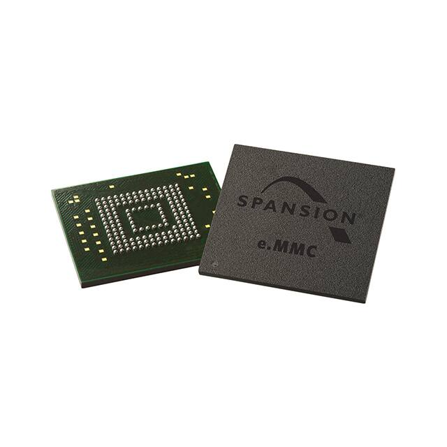
�S4041-1B1
8 GB / 16 GB, 3.0 V e.MMC Flash
Features
Key Supported Features
■
e.MMC 4.51 Specification
on compatible
com
❐ Backward compatible
patible
atible with prev
previ
previous e.MMC specifications
■
Storage temperature
erature
era
ure
❐ �40 °C to
o +85
+ 5 °C
°
■
Operating
g voltage
volt
olt
❐ VCCQ: 1.7
7 V - 1.95 V or 2.
2.7 V - 3.6
.6 V
❐ VCC: 2
2.7 V - 3.6 V
■
Density:
y: 8/16
6 GB of data storage
s ora
orage
■
Data bus width:
❐ SDR mode: 1 bit, 4 b
bit, 8 bit
❐ DDR mode: 4 bit,
t, 8 bit
it
❐ HS200 mode: 4 bit, 8 bit
it
■
Clock frequency: 52 MHz,
Hz, 200 MH
MHz
z (e.MMC 4.51)
❐ SDR mode: up to 52 MHz
❐ DDR mode: up to 52 MHz
❐ HS200 mode: up to 200 MHz
■
BGA packages
❐ 153-ball VFBGA: 13 mm u 11.5 mm u 1.0 mm
❐ 100-ball LBGA: 18 mm u 14 mm u 1.4 mm
■
Operating temperature range
❐ Embedded: �25 °C to +85 °C
❐ Industrial: �40 °C to +85 °C
Cypress Semiconductor Corporation
Document Number: 002-02760 Rev. *H
•
■
Boot Operation
■
Partition Management
■
Boot Area Partition
■
Replay Protected Memory Block (RPMB)
■
Sleep (CMD5)
■
Sanitize
■
Trim
■
High Priority Interrupt
■
Background Operations
■
Auto Background Operations
■
Hardware Reset
Ha
■
HS200
HS20
H
0
■
Health
ealth
e
th Monitoring
Performance
Perfo
Pe
fo manc
■
Sequential
S
quentia Read (MB/s): 120
■
Sequential Write (MB/s):
Seque
B/s): 20
❐B
Based on 16-GB
B device
❐ Bus in x8 I/O
O and
d HS2
HS200 mo
modes
■
Random Read
ead (IOPS): 5000
■
Random
om
m Write (IOPS
(IOPS): 1400
198 Champion Court
•
San Jose, CA 95134-1709
•
408-943-2600
Revised March 03, 2016
�S4041-1B1
General Description
Cypress® e.MMC is a managed NAND memory solution designed for embedded applications. Cypress e.MMC includes a flash
controller and a standard MLC NAND flash memory, and is compatible with the JEDEC JESD84-B451 with backwards compatibility
to previous e.MMC specifications.
Designed for faster throughput and large data transfer, Cypress e.MMC offers high performance, great reliability, and minimal latency.
ormance Cypress’s e.MMC offers optimum power management features resulting in reduced power
In addition to higher performance,
consumption, making
for mobile applications.
g it an ideal solution
sol
timized Cypress
Cypr
In addition, highlyy optimized
firmware fully utilizes the MLC NAND capabilities leveraging wear-leveling, defect management,
garbage collection,
and ECC to enhance
product life.
ction,
cti
n, a
enha
e
ha
The Cypress
array of the JEDEC e.MMC features including HS200, high priority interrupt (HPI),
ss e.MMC
.MMC product family
fam offers
rs a vast
v
boot partitions,
hardware reset, and power off notification.
ions,
s, RPMB partitions,
partition background
b kground
ground operations,
o
Combined
d with
ith an advanced e.MMC
e.MMC feature
eature set and
a Cypress’s commitment to quality, Cypress e.MMC is ideal for industrial applications as well as set top boxes,
gaming
and consumer electronic devices.
boxes
bo
gam
aming
ng consoles,
oles, a
ole
Cypress
s Product Offe
Offering
erin
The Cypress e.MMC product
uct offering includes:
inc
inclu
8/16 GB in 153-FBGA
153
153(13 mm u 11.5 mm) and 100-BGA (18 mm u 14 mm) packages.
■
8 GB: S40410081
❐ 153 VFBGA (13 u 11.5
11.
1.5 u 1.0,
1 0 0.5
.5 mm
mm ball pitch)
❐ 100 LBGA (18 u 14 u 1.4, 1.0 mm
mm ball pitch)
h)
■
16 GB: S40410161
❐ 153 VFBGA (13 u 11.5 u 1.0, 0.5
.5
5 mm ball pitch)
❐ 100 LBGA (18 u 14 u 1.4, 1.0 mm
m ball pitch)
pitch
Document Number: 002-02760 Rev. *H
Page 2 of 29
�S4041-1B1
Contents
Package Configurations .................................................. 4
Architecture ...................................................................... 6
Key Supported e.MMC Features ..................................... 7
Boot Operation ............................................................ 7
Partition Management
................................................. 7
nt ........
.......
Sleep (CMD5) .........................
..............................................................
........................
8
High Priority
......................................... 8
y Interrupt
rrupt (HPI) .....
Background
............................................... 8
und
nd Operations .....
...........
Auto Background
8
ackground
ground Operation
Operations .......................................
..
Trim .............................................................................
8
......................................
...........................
............
..........
Sanitize
........................................................................
8
tize
ize .........................
...............................
...................
....................
...
Hardware
..........................................................
8
dware
re Reset .......
..............
.........................
............
Health
........................................................
9
th Monitoring .......
........
...............................
..............................
................
Field Firmware Upda
Update
................................................
9
e ...............................
................................
..
.............
Register Values
ues ...............................................................
..................................
...................................
............
.............
............ 10
Operating Conditions
..................................
ions
ons Register ........
..........
................
...
........... 10
Card Identification
Register
.......................................
io
on Reg
eg
..........
..................
..
............ 10
1
Product Table ............................................................
...........................
............................
...........
...................
............ 1
10
Card Specific Data Register .....
......................................
....
............................... 11
Extended CSD Register (EXT_CSD)
........................ 12
(E
(EX
CSD) ................
.................
AC Parameter ..................................................................
...........................
............................
18
Bus Timing ................................................................
............................
.......................... ....
..... 18
8
High Speed Timing ....................................................
18
........................ ....
........
.. 1
Document Number: 002-02760 Rev. *H
Backward Compatible Timing .................................... 19
DDR Interface Timing ................................................ 19
Timing Specifications for HS200 Mode ..................... 20
Signal Levels ............................................................. 23
Open-Drain Mode Bus Signal Level .......................... 23
Push-Pull Mode Bus Signal Level —
High Voltage e.MMC ................................................. 23
Push-Pull Bus Signal Level —
Dual Voltage e.MMC ................................................. 23
DC Parameter .................................................................. 24
Supply Voltage .......................................................... 24
Bus Operating Condition ........................................... 24
Power Consumption (Temperature = 25 °C) ............. 24
Ordering Information ...................................................... 25
Valid Combinations ................................................... 25
Package Diagrams .......................................................... 26
Document History Page ................................................. 28
Sales, Solutions, and Legal Information ...................... 29
Worldwide Sales and Design Support ....................... 29
Products
.................................................................... 29
P
PSoC®
Solutions ...................................................... 29
PS
S
Cypress
Developer Community ................................. 29
Cyp
p
Technical
Support ..................................................... 29
Te
ec
Page 3 of 29
�S4041-1B1
Package Configurations
Figure 1. FBGA 153 (Top View, Balls Down)
1
2
3
4
5
6
7
8
9
10
11
12
13
14
A
NC
NC
NC
NC
NC
NC
NC
NC
NC
DAT3 DAT4 DAT5 DAT6 DAT7 NC
NC
DAT0 DAT1 DAT2 RFU RFU
NC
NC
NC
NC
NC
NC
NC
NC
VDDI
NC VSSQ NC VCCQ NC
NC
NC
NC
NC
NC
NC
NC
NC
NC
NC
NC
NC
NC
B
C
D
NC
NC
E
NC
NC
NC
RFU VCC VSS RFU RFU
RFU
NC
NC
NC
NC
NC
VCC
RFU
NC
NC
NC
NC
NC
RFU
VSS
RFU
NC
NC
NC
F
G
H
NC
NC
N
C
NC
RFU
VSS
NC
NC
NC
NC
NC
N
NC
RFU
VCC
NC
NC
NC
NC
NC
NC
C
RST_N RFU RFU VSS VCC RFU
RST
RST_
NC
NC
NC
NC
NC
NC
NC
NC
NC
NC
C
NC
NC VCCQ CM
CMD
MD CL
CLK
L
J
K
L
M
NC
NC
NC
NC
NC
NC
NC
NC
NC
NC
NC
NC
NC
NC
NC
NC
NC
NC
RFU
NC
NC
NC
NC
N
N VSSQ
NC
Q NC VCCQ
QV
VSSQ NC
P
NC
NC VC
VCCQ
CC VSSQ VCCQ
C
VSSQ RFU
Balls Down)
Figure
igure 2.
2 BGA
A 100 (Top View,
Vie B
1
2
NC
NC
3
4
5
6
7
8
9
10
N
NC
NC
A
B
NC
NC
C
D
RFU
RFU
RFU
RFU
RFU
RFU
RFU
RFU
RFU
RFU
VDDII
RFU
RFU
R
RFU
RFU
U
RFU
VCC
VCC
VCC
VCC
VCC
C
VCC
CC
C
VCC
CC
VCC
VSS
VSS
VSS
VSS
VSS
VSS
VSS
SS
VSS
VSSQ
VCCQ
RFU
RFU
RFU
RFU
VCCQ
VC
VSSQ
Q
RFU
RFU
RFU
RFU
RFU
RFU
RFU
RFU
DAT0
DAT2
RFU
RFU
RFU
RFU
DAT5
DAT7
VCCQ
VSSQ
VCCQ
RFU
RFU
VCCQ
VSSQ
VCCQ
RFU
RFU
VSSQ
RST_N
RFU
VSSQ
RFU
RFU
DAT1
DAT3
RFU
RFU
RFU
RFU
DAT4
DAT6
VSSQ
VCCQ
RFU
CMD
CLK
RFU
VCCQ
VSSQ
E
F
G
H
J
K
L
M
N
P
T
NC
NC
U
NC
Document Number: 002-02760 Rev. *H
NC
NC
NC
Page 4 of 29
�S4041-1B1
Table 1. Pin Description
Pin Name
Type
DAT0 - DAT7
I/O
Bidirectional data channels used for data transfers
Description
CMD
I/O
Bidirectional command channel used for device initialization and command transfers
CLK
Input
Clock input
RST_N
Input
Hardware reset
H
VCC
Power
Supply
voltage for the flash memory
S
VCCQ
Q
Power
Supply
voltage for the memory controller and MMC interface
ply vo
VDDI
DI
D
Power
wer
er
Internal
power
nternal
nte
na powe
we node. Connect capacitor to ground.
VSS
SS
S
Power
Power
Ground
forr the flash memory
Gro
pin fo
pi
VSSQ
SQ
Power
Powerr
Ground
for the memory controller and MMC interface
Gr
Gro
pin fo
pi
NC
—
Not connected
connec
nec
RFU
—
Reserved
for
Rese
R
e
or future
uture use.
us Do
D not connect.
Document Number: 002-02760 Rev. *H
Page 5 of 29
�S4041-1B1
Architecture
Cypress e.MMC is an embedded non-volatile storage solution with a MultiMediaCard (MMC) interface, a high performance memory
controller, and state of the art flash memory all supported by Cypress optimized flash management software. Based on the JEDEC
industry-standard MMC System Specification v4.51, the Cypress e.MMC product family is offered in standard JEDEC BGA packages.
Figure 3 represents the basic block diagram of the Cypress e.MMC.
Figure 3. Cypress e.MMC Architecture
VCC
C
VDDI
DDI
DD
CREG
CLK
CMD
CM
DAT[7:0]
0]
Core Regulator
C
Block
k
Core
Logic B
NAND I/O Block
Reset
Rese
ese
MMC
C I/O Blo
Block
o
VCCQ
NAND Data
Memory
NAND Control
e.MMC
..MMC
C Controller
tro
troller
Document Number: 002-02760 Rev. *H
Page 6 of 29
�S4041-1B1
Key Supported e.MMC Features
Cypress e.MMC supports the JEDEC JESD84-B451 specification.
Boot Operation
Cypress e.MMC supports boot mode as well as alternate boot mode. Boot operations can be performed at high speed and dual data
rate timings.
Figure 4. MultiMediaCard State Diagram (Boot Mode)
CLK
CMD
CMD1
DAT[0]
S
010
E
S
512 bytes E
+ CRC
S
512 bytes
+ CRC
RESP
CMD2
RESP
CMD3 RESP
E
Boot terminated
Min 8 clocks + 48 clocks = 56 clocks required from
CMD signal high to next MMC command
50 m
ms
max
00 ms ttyp
100
0 ms m
Partition
150
max (Boot from Boot Partition)
rom
om User
Us Area)
1 ssec ma
max (Boot from
Figure
MultiMediaCard
State
Boot Mode)[1]
Fi
Fig
e 5. M
Media
MediaCard
ate Diagram (Alternative
(
CLK
CMD
CMD0
(1)
CMD0/Reset
D0/Rese
D
se
DAT[0]
Min. 74 clocks
required after
power is stable
to start boot
command
S
010
E
S
512 bytes E
5
51
+ CRC
S
CMD1 RESP
CMD2 RESP
CMD3 RESP
512
12 bytes
es E
C
+ CRC
50 ms
max
100 ms typ
150 ms max (Boot from Boot Partition)
1 sec max (Boot from User Area)
Partition Management
e.MMC specifications allow for the device to have the following partitions:
ns: a User Data Area
Are for general
ral purpose storage,
sto
two boot
ock
ck (RPMB)
(RPM for data management
gement in a replay
rep ay protected
p
pr
partitions for storing boot images, and the Replay Protected Memory Block
and
authenticated manner.
The Cypress e.MMC device can be configured as below:
■
Factory configuration supplies two boot partitions size of 4 MB each and one RPMB partition
artition size of 4 MB. These partitions a
are
configured in Enhanced (SLC) mode for higher reliability.
■
The host can create up to four General Purpose Partitions within the User Data Area. These partitions
ons can be configure
configured in Enhanced
rtition.
tition. These attribute
attributes can be
(SLC) mode or Default (MLC) mode. The host will also need to configure the size of each partition.
programmed by the host only once in the device life-cycle (one-time programmable).
■
In addition to the General Purpose Partitions the host can also configure a segment of the User Data Are
Area to be accessed in
es
s can b
Enhanced (SLC) mode. The host will need to specify the starting location and size. These attributes
be programmed by the
host only once in the device life-cycle (one-time programmable).
Note
1. CMD0 with argument 0xFFFFFFFA.
Document Number: 002-02760 Rev. *H
Page 7 of 29
�S4041-1B1
Table 2. Partition Type
Partition
NAND Mode
Boot Area 1
SLC Mode
Boot Area 2
SLC Mode
RPMB Area
RPM
SLC Mode
General Purpose Partition
Ge
User Data
Area
Dat
ata Are
MLC or SLC Mode
Enhanced
En
h
SLC Mode
Default
De
e
MLC Mode
Figure 6. Partitions
General
neral Purp
ne
Purpose
rp
Partition
Boot 1
Boot 2
RPMB
PM
GPA
PA 1
GPA
A2
GPA 3
GPA 3
Enhanced User Data Area (SLC mode) Default User Data Area (MLC mode)
User Data Area
Sleep (CMD5)
Sleep/Awake (CMD5) is used to switch
itch the device be
between
n Sleep
ep and Stand
Stan
Standby mode. During the Sleep state, VCC can be switched
hile a device is in Sleep
S ep mode
ode it can only
on respond
r
off for maximum power savings. While
to the Reset (CMD0) and Sleep/Awake (CMD5)
commands.
High Priority Interrupt (HPI)
High Priority Interrupt (HPI) is intended to suspend
nd
d an
n ongoing opera
operation while
hile allowing
allo
for a high priority read operation to be
performed.
Background Operations
e.MMC devices are equipped with a Background Operations
ti
feature
ure
re (see Table 7 on page
ge 12). When enabled,
e
Background Operations
allow the e.MMC device to perform a number of routine data maintenance
operationss such as wearr leveling,
aintena
intena
leveli
elin garbage collection, erase,
and compaction while the host CPU is not being serviced.
Auto Background Operations
Auto Background Operations is a feature that allows the e.MMC device
evice to fully manage
e backg
back
background operations
erations without
w
any requiretions
ions are required at specified
s
tervals
ervals and initiate
init
ments from the Host. The e.MMC device will check if background operations
intervals
background
operations if needed. This frees the host from having to develop software
re to
t manage
man
these maintenance
nance tasks and en
ensure that the
e.MMC device is operating at the optimum performance levels. Issuing any command
operations
comman while auto background
ackgro
ations are occurring
will stop the current background operation activities. There will be a maximum
m latency
latenc of 40 ms if auto
au background
aut
ound operation
operatio
operations are
interrupted by any read or write command from the host.
This feature is enabled on default and can be configured through the CMD56 command. A sepa
separate application
cation note is available with
the full details of the CMD56 command. A non-disclosure agreement (NDA) is required
this application
d to view
vi
pplication note.
no Contact
Contac your
nearest Cypress sales office for more information.
Trim
Similar to the Erase operation, the Trim function (Table 7 on page 12) performs a targeted erase on specif
specific write blocks. Data that is
no longer needed, designated by the host, will be erased during background erase events.
Sanitize
Sanitize (Table 7 on page 12) is intended for applications with high security requirements that can afford the performance impact. This
command is used in conjunction with standard Erase or Trim operations and requires the device to physically remove data from the
unmapped user address space. The busy line will be asserted once the Sanitize operations begin and will remain busy until the
operation has been completed or interrupted.
Hardware Reset
Used by the host to reset the device, hardware reset moves the device into a pre-idle state and disables the power-on period write
protection on blocks that were set at power-on as write protected.
Document Number: 002-02760 Rev. *H
Page 8 of 29
�S4041-1B1
Health Monitoring
Health Monitoring is a proprietary feature of the Cypress e.MMC product that provides useful information about the life span of the
NAND flash component. The host can query for the device’s health by using the CMD56 command to get information such as the
number of bad blocks and the number of erase cycles for each block. EXT_CSD registers [269:254] also contain valuable device
health information. A separate application note is available with the full details of the CMD56 command and EXT_CSD registers
[269:254]. A non-disclosure agreement (NDA) is required to view this application note. Contact your nearest Cypress sales office for
more information.
Field Firmware
e Up
Update
date
Field Firmware
e Update
pdate is a feature
featu tthat allows the host to upload a new version of the firmware to the e.MMC. This can be done by
evice
ce into FFU mode and
an performing
for
o
setting the device
writes with the arguments defined in the FFU_ARG register. A separate application
note is available
ilable
lable
le with the full deta
details o
of this
s featu
feat
feature. A non-disclosure agreement (NDA) is required to view this application note. Contact
your nearest
est Cypress sales office
e
off ce for more
re information.
infor
Document Number: 002-02760 Rev. *H
Page 9 of 29
�S4041-1B1
Register Values
Operating Conditions Register
Operation Conditions Register (OCR) stores the e.MMC voltage profile. In addition, it contains the status bit (31) which is set when
the device power up has been completed.
Table 3. OCR Register
Field Description
OCR Slice
Reserved
Value
[6:0]
00 00000b
1.95
5 rrange
VCCQ: 1.7 - 1
[7]
Dual Voltage: 1b
0 - 2.6
.6 range
VCCQ: 2.0
[14:8]
000 0000b
7-3
3.6 range
VCCQ: 2.7
[23:15]
1 1111 1111b
d
Reserved
[28:24]
0 0000b
Access Mode
ode
[30:29]
Sector Mode: 10b
[31]
�
[2]
2]
e.MMC power up status
(busy)
us bitt (b
(
Card Identification
n Register
R gister
The Card Identification Register
egister (CID
(CI
(CID)) con
contains
s the card iden
identification
tion inf
information used during the card identification phase.
Table 4. CID Register
Field
ield
eld ID
Width
W
th
CID Slice
ce
c
CID Value
Manufacturer ID
Field Name
MID
8
20]
2
[127:120]
01h
Card BGA
CBX
2
[113:112]
3:112]
3:1
2]
01b
OEM/Application ID
OID
8
[111:1
[11
[111:104]
:104]]
00h
Product Name
PNM
48
8
[103:56]
[1
[103:56
3:56]
See Product Table.
Product Revision[5]
PRV
8
[55:48
[55
[55:48]
48
�
PSN
32
[47:16]
[47
32-bit
bit unsigned
uns
ns
d binary
b ry integer
i
assigned at random
MDT
8
[15:8]
[1
CRC
7
[7:1]
1]
�
�
—
1
[0]
[0
Always
ways 1
way
Product Serial Number
Manufacturing Date
[4]
[4]
CRC7 Checksum
Not Used
Product Table
Table 5. Product Table
Cypress Part Number
Density
Product
Prod
P
odu Name
e in CID Register
ster
ter (PN
(PNM)
PN
S40410081
8 GB
08” – 533430343038h
08
53343
343
h
“S40408”
S40410161
16 GB
“S40416”
40416
40
16” – 533430343136h
533
3343034
034
Notes
2. Reserved bits should be read at ‘0’.
3. R = Read only. R/W = One time programmable and readable. R/W/E = Multiple writable with value kept after power failure, hardware reset assertion and any CMD0
reset and readable.
4. VDD represents the total consumed current for VCC and VCCQ.
Document Number: 002-02760 Rev. *H
Page 10 of 29
�S4041-1B1
Card Specific Data Register
Card Specific Data (CSD) Register contains the e.MMC access information. It includes data format, error correction, transfer speeds,
and access times. It also includes information as to whether the DSR register can be accessed.
Table 6. CSD Register
Size (Bits)
Cell Type
CSD Slice
CSD Value
CSD Structure
Field Name
CSD_STRUCTURE
2
R
[127:126]
3h
System Specification
Version
ation Ver
atio
SPEC_VERS
4
R
[125:122]
4h
2
R
[121:120]
—
TA
TAAC
8
R
[119:112]
4Fh
Data Read
ad Ac
Access Time 2 in CL
CLK cyc
cycles
es
NSAC
N AC
(NSAC*100)
100))
1
8
R
[111:104]
01h
Reserved
Field ID
[5]
d Access
A
Accce Time 1
Data Read
—
Maximum
m Buss Clock Frequency
Frequ
equ ncy
TRAN_SPEED
TRAN
TR
N
8
R
[103:96]
32h
Card Command
mand Classes
Clas
CCC
CC
12
R
[95:84]
0F5h
Maximum Read Blockk Length
L
Leng
ng
READ_BL_LEN
AD_BL_LEN
AD
_BL_LE
4
R
[83:80]
9h
Partial Blocks For Rea
Allowed
Read Allo
READ_BL_PARTIAL
EAD_
E
_
AR
RTIA
A
1
R
[79:79]
0h
Write Block Misalignment
nt
WRITE_BLK_MISALIGN
RITE_
R
_ K_
K_MIS
MIS
1
R
[78:78]
0h
Read Block Misalignment
READ_BLK_MISALIGN
AD_B
AD
BL
SALIGN
SALIG
1
R
[77:77]
0h
Dsr Implemented
DSR_IMP
R_IMP
R_
MP
1
R
[76:76]
0h
2
R
[75:74]
—
[5]
—
Reserved
Device Size
*C
ZE
*C_SIZE
12
R
[73:62]
FFFh
Maximum Read Current at VDD min
VDD_R_CURR_MIN
_R_C
_R
C
3
R
[61:59]
7h
Maximum Read Current at VDD max
VDD_R_CURR_MAX
_R_C
_
CU
MAX
3
R
[58:56]
7h
Maximum Write Current at VDD min
VDD_W_CURR_MIN
W_CURR_MIN
W_
_MIN
3
R
[55:53]
7h
Maximum Write Current at VDD max
VDD_W_CURR_MAX
AX
3
R
[52:50]
7h
Device Size Multiplier
C_SIZE_MULT
3
R
[49:47]
7h
Erase Group Size
ERASE_GRP_SIZE
ZE
E
5
R
[46:42]
[46
1Fh
Erase Group Size Multiplier
ERASE_GRP_MULT
5
R
[41:37]
37]
1Fh
Write Protect Group Size
WP_GRP_SIZE
5
R
[36:32]
8 GB: 0Fh
16 GB: 1Fh
Write Protect Group Enable
WP_GRP_ENABLE
1
R
[31:31]
1]
1h
Manufacturer Default
DEFAULT_ECC
2
R
[30:29]
30:29]
30:
9]
0h
Write Speed Factor
R2W_FACTOR
3
R
[28:26]
[28:26
26
2h
Maximum Write Data Block Length
WRITE_BL_LEN
4
R
[25:22]
[25:
9h
Partial Blocks For Write Allowed
WRITE_BL_PARTIAL
1
R
[21:21]
21]
1]
0h
[5]
4
R
[20:17]
—
Content Protection Application
CONTENT_PROT_APP
1
R
[1
[16:16]
0h
File Format Group
FILE_FORMAT_GRP
1
R/W
[1
[15:15]
0h
Copy Flag (OTP)
COPY
1
R/W
[14:14]
0h
Permanent Write Protection
PERM_WRITE_PROTECT
1
R/W
[13:13]
0h
Reserved
—
Notes
5. Reserved bits should be read at ‘0’.
6. R = Read only. R/W = One time programmable and readable. R/W/E = Multiple writable with value kept after power failure, hardware reset assertion and any CMD0
reset and readable.
7. VDD represents the total consumed current for VCC and VCCQ.
Document Number: 002-02760 Rev. *H
Page 11 of 29
�S4041-1B1
Table 6. CSD Register (Continued)
Size (Bits)
Cell Type
CSD Slice
CSD Value
Temporary Write Protection
Field Name
TMP_WRITE_PROTECT
Field ID
1
R/W/E
[12:12]
0h
File Format
FILE_FORMAT
2
R/W
[11:10]
0h
ECC Code
ECC
2
R/W/E
[9:8]
0h
Calculated CRC
CRC
7
R/W/E
[7:1]
—
1
—
[0]
Always 1
Not Used
—
Notes
ed bits
ts should be read at ‘0’.
‘0
5. Reserved
ad only.
nly. R/W = One time progr
prog
mable
e and readable.
reada
readab
6. R = Read
programmable
R/W/E = Multiple writable with value kept after power failure, hardware reset assertion and any CMD0
reset an
and
nd readable.
re
e
presents
ents the total consum
co
consumed cu
current
nt ffor VCC an
and
nd VC
.
7. VDD represents
CCQ
Extended CSD Reg
Re
Register
ter (EXT_
(EXT_CSD)
SD)
The Extended CSD Register
egister
eg
ter defines the
e e.MMC
e
C selected modes
mod and properties. It is 512 bytes long. The most significant 320 bytes,
mode
also know as Properties
rties
ties segment,
egment, define
def
the e.MMC
.MMC
MMC capabilities
capabilitie and cannot be modified by the host. The remaining 192 bytes define
des and
nd can b
be m
e.MMC operating modes
modified by the host via a Switch command.
Table 7. Extended CSD Register (EXT_CSD)
(EXT_ D)
Field Name
Field ID
F
Reserved[8]
—
Size
(B
B
(Bytes)
Cell Type
EXT_CSD
Slice
Value
6
—
[511:506]
—
Extended Security Commands Error
EXT SEC IT
TY_E
_E
EXT_SECURITY_ERR
1
R
[505]
00h
Supported Command Sets
T
S_CMD_SET
1
R
[504]
01h
HPI Features
RES
R
S
HPI_FEATURES
1
R
[503]
01h
Background Operations Support
PPORT
PP
BKOPS_SUPPORT
1
R
[502]
01h
Max Packed Read Commands
EA
MAX_PACKED_READS
1
R
[501]
3Ch
Max Packed Write Commands
S
MAX_PACKED_WRITES
1
R
[500]
3Ch
Data Tag Support
DATA_TAG_SUPPORT
1
R
[[499]
01h
Tag Unit Size
TAG_UNIT_SIZE
1
R
[498
98
[498]
03h
Tag Resources Size
TAG_RES_SIZE
1
R
[4
[497]
00h
Context Management Capabilities
CONTEXT_CAPABILITIES
1
R
96]
6]
[496]
05h
Large Unit Size
LARGE_UNIT_SIZE_M1
1
R
5]
[495]
8G
Gb: 03h
G 07h
16 Gb:
Extended Partitions Attribute Support EXT_SUPPORT
1
R
[ 94]
[494]
h
03h
Supported Modes
SUPPORTED_MODES
1
R
3]
[493]
0
01h
FFU Features
FFU_FEATURES
1
R
492]
492
[492]
00h
Operation Codes Timeout
OPERATION_CODE_TIMEOUT
1
R
[491]
00h
Notes
8. Reserved bits should be read at 0, unless otherwise specified.
9. Set to 0 after power on, hardware reset or software reset selecting backward compatibility interface timings. If the host changes the value to 1, the device will operate
in high-speed mode and finally, if host changes the value to 2, HS200 interface timings will be used.
10. Set to 0 after power up and can be changed via a Switch command.
11. R = Read only.
R/W = One time programmable and readable.
R/W/E = Multiple writable with value kept after power failure, hardware reset assertion and any CMD0 reset and readable.
R/W/C_P = Writable after value cleared by power failure and hardware reset assertion (the value not cleared by CMD0 reset) and readable.
R/W/E_P = Multiple writable with value reset after power failure, hardware reset assertion and any CMD0 reset and readable.
W/E_P = Multiple writable with value reset after power failure, hardware reset assertion and any CMD0 reset and not readable.
12. Value depends on state of the device.
13. Value depends on the firmware that the device is loaded with.
Document Number: 002-02760 Rev. *H
Page 12 of 29
�S4041-1B1
Table 7. Extended CSD Register (EXT_CSD) (Continued)
Field Name
Field ID
Size
(Bytes)
Cell Type
EXT_CSD
Slice
Value
FFU Argument
FFU_ARG
4
R
[490:487]
Normal mode:
00000000h
FFU mode:
0000FFFFh
181
—
[486:306]
—
4
R
[305:302]
00000000h
32
—
[301:270]
—
Reserved[8]
Se tors Correctly
Number of FW Sectors
Programmed
NUMBER_OF_FW_SECTORS_
CORRECTLY_PROGRAMMED
Reserved[8]
—
fe Ti
nT
Type
pe B
Device Life
Time Estimation
DEVICE_LIF
EVIC LIF
DEVICE_LIFE_TIME_EST_TYP_B
1
R
[269]
01h
iffe Tim
mation Ty
matio
eA
Device Life
Time Estimation
Type
D
E_LIF
E_
F
DEVICE_LIFE_TIME_EST_TYP_A
1
R
[268]
01h
nformation
nf
Pre-EOL Information
P
PR
EOL_
EO
_I
PRE_EOL_INFO
1
R
[267]
01h[12]
Optimal Read Size
OPTIMAL_READ_SIZE
OPTIMA
IMAL REA
EAD_SIZE
E
1
R
[266]
01h
Optimal Write Size
OP
P
L_W
_WR
RITE_SIZ
SIZE
OPTIMAL_WRITE_SIZE
1
R
[265]
04h
e
Optimal Trim Unit Size
OP
O
L_TR
L
R
IT_S
IT
S
OPTIMAL_TRIM_UNIT_SIZE
1
R
[264]
01h
Device Version
DEV
DEVI
_V
VERS
S N
DEVICE_VERSION
2
R
[263:262]
B101h
Firmware Version[13]
FIRMWARE_VERSION
FIR
R
E_VE
E
E
8
R
[261:254]
—
Reserved
[8]
1
—
[253]
—
Cache Size
HE IZE
CACHE_SIZE
—
4
R
[252:249]
00000000h
Generic CMD6 Timeout
ENER
MD6_
M
6_
GENERIC_CMD6_TIME
1
R
[248]
19h
FF_L
F
L
Power Off Notification (Long) Timeout POWER_OFF_LONG_TIME
1
R
[247]
FFh
Background Operations Status
ATUS
A
S
BKOPS_STATUS
1
R
[246]
00h
Number Of Correctly Programmed
Sectors
Y_PRG_SECTO S_N
S_NU
U
CORRECTLY_PRG_SECTORS_NU
M
4
R
[245:242]
00000000h
1st Initialization Time after Partitioning INI_TIMEOUT_PA
1
R
[241]
32h
Reserved[8]
1
—
[240]
—
Power Class for 52 MHz, DDR at 3.6 V PWR_CL_DDR_52_360
1
R
[23
239
[239]
44h
Power Class for 52 MHz, DDR at 1.95
PWR_CL_DDR_52_195
V
1
R
[2
[238]
99h
Power Class for 200 MHz at 1.95 V
PWR_CL_200_195
1
R
7]]
[237]
AAh
Power Class for 200 MHz at 1.30 V
PWR_CL_200_130
1
R
36]
6]
[236]
0
00h
Minimum Write Performance for
8-bit at 52 MHz in DDR mode
MIN_PERF_DDR_W_8_52
1
R
[235
35]
[235]
08h
Minimum Read Performance for
8-bit at 52 MHz in DDR mode
MIN_PERF_DDR_R_8_52
1
R
[23
[234]
08h
1
—
[233]
—
—
Reserved[8]
—
Notes
8. Reserved bits should be read at 0, unless otherwise specified.
9. Set to 0 after power on, hardware reset or software reset selecting backward compatibility interface timings. If the host changes the
to 1, the device will operate
e value
v
in high-speed mode and finally, if host changes the value to 2, HS200 interface timings will be used.
10. Set to 0 after power up and can be changed via a Switch command.
11. R = Read only.
R/W = One time programmable and readable.
R/W/E = Multiple writable with value kept after power failure, hardware reset assertion and any CMD0 reset and readable.
R/W/C_P = Writable after value cleared by power failure and hardware reset assertion (the value not cleared by CMD0 reset) and readable.
R/W/E_P = Multiple writable with value reset after power failure, hardware reset assertion and any CMD0 reset and readable.
W/E_P = Multiple writable with value reset after power failure, hardware reset assertion and any CMD0 reset and not readable.
12. Value depends on state of the device.
13. Value depends on the firmware that the device is loaded with.
Document Number: 002-02760 Rev. *H
Page 13 of 29
�S4041-1B1
Table 7. Extended CSD Register (EXT_CSD) (Continued)
Field Name
Field ID
Size
(Bytes)
Cell Type
EXT_CSD
Slice
Value
Trim Multiplier
TRIM_MULT
1
R
[232]
0Fh
Secure Feature Support
SEC_FEATURE_SUPPORT
1
R
[231]
55h
Secure Erase Multiplier
SEC_ERASE_MULT
1
R
[230]
06h
Secure TRIM Multiplier
tiplie
iplier
SEC_TRIM_MULT
1
R
[229]
09h
on
Boot Information
BOOT_INFO
1
R
[228]
07h
—
1
—
[227]
—
tition S
Boot Partition
Size
BOOT_SIZ
BOOT_SIZE_MULTI
1
R
[226]
20h
Size
Access S
ACC_SIZ
ACC_SIZE
1
R
[225]
8 GB: 06h
16 GB: 07h
city Erase Unit
Un Size
ize
High Capacity
HC_ERASE
HC
HC_ERAS
ER
RP_SIZ
HC_ERASE_GRP_SIZE
1
R
[224]
8 GB: 08h
16 GB: 10h
High Capacity Erase Time Out
ER
ERA
IMEOUT_MULT
ERASE_TIMEOUT_MULT
1
R
[223]
01h
Reserved[8]
Reliable Write Sectorr Countt
RE
R_SE
REL_WR_SEC_C
1
R
[222]
01h
tec
ect Group
High Capacity Write Protect
Size
HC_WP_GRP_SIZE
1
R
[221]
02h
Sleep Current [VCC]
S_
S_C_VCC
_
1
R
[220]
08h
Sleep Current [VCCQ]
S_C_VCCQ
_C_VCCQ
1
R
[219]
08h
PRODUCTION_STATE_AWARENES
PRODUCTION_S
_STATE_AWARENES
TATE_AWARENES
Production State Awareness Timeout
S_TIMEOUT
S TIMEO
1
R
[218]
14h
Sleep/awake Time Out
1
R
[217]
10h
1
—
[216]
0Fh
Reserved
S_A_TIMEOUT
OU
UT
[8]
Sector Count
—
SEC_COUNT
Reserved[8]
—
4
R
[215:212]
8 GB:
00E90000h
16 GB:
01D20000h
1
—
[211]
—
Minimum Write Performance for
8-bit at 52 MHz
MIN_PERF_W_8_52
1
R
[210
10]
[210]
08h
Minimum Read Performance for
8-bit at 52 MHz
MIN_PERF_R_8_52
1
R
209]
09]
[209]
08h
Minimum Write Performance for
4-bit at 52 MHz or 8-bit at 26 MHz
MIN_PERF_W_8_26_4_52
1
R
[208]
8]
08h
0
Minimum Read Performance for
4-bit at 52 MHz or 8-bit at 26 MHz
MIN_PERF_R_8_26_4_52
1
R
[207]
[207
07
08h
Minimum Write Performance for
4-bit at 26 MHz
MIN_PERF_W_4_26
1
R
[206]
206]
20
08h
Notes
8. Reserved bits should be read at 0, unless otherwise specified.
9. Set to 0 after power on, hardware reset or software reset selecting backward compatibility interface timings. If the host changess the valu
value to 1, the device will operate
in high-speed mode and finally, if host changes the value to 2, HS200 interface timings will be used.
10. Set to 0 after power up and can be changed via a Switch command.
11. R = Read only.
R/W = One time programmable and readable.
R/W/E = Multiple writable with value kept after power failure, hardware reset assertion and any CMD0 reset and readable.
R/W/C_P = Writable after value cleared by power failure and hardware reset assertion (the value not cleared by CMD0 reset) and readable.
R/W/E_P = Multiple writable with value reset after power failure, hardware reset assertion and any CMD0 reset and readable.
W/E_P = Multiple writable with value reset after power failure, hardware reset assertion and any CMD0 reset and not readable.
12. Value depends on state of the device.
13. Value depends on the firmware that the device is loaded with.
Document Number: 002-02760 Rev. *H
Page 14 of 29
�S4041-1B1
Table 7. Extended CSD Register (EXT_CSD) (Continued)
Field Name
Minimum Read Performance for
4-bit at 26 MHz
Size
(Bytes)
Cell Type
EXT_CSD
Slice
Value
MIN_PERF_R_4_26
1
R
[205]
08h
—
1
—
[204]
—
Field ID
Reserved[8]
Power Class for 26 MHz at 3.6 V
PWR_CL_26_360
1
R
[203]
22h
MHz at 3.6 V
Power Class forr 52 MH
PWR_CL_52_360
1
R
[202]
22h
fo 26 MHz at 1.95 V
Power Classs for
_
PWR_CL_26_195
1
R
[201]
77h
ss fo
or 52 MHz at 1.95
95
5V
Power Class
for
PW
WR_CL
CL_
PWR_CL_52_195
1
R
[200]
77h
Switc
tc
Partition S
Switching
Timing
PARTITION_
ARTIT N_
PARTITION_SWITCH_TIME
1
R
[199]
03h
tterrup
upt Busy Timing
Tim g
Out-of-Interrupt
O
F_IN
F
NT
OUT_OF_INTERRUPT_TIME
1
R
[198]
04h
Strength
I/O Driver Str
DRIVER
DRIVER_ST
ST
DRIVER_STRENGTH
1
R
[197]
0Fh
Card Type
CARD_T
ARD_T E
CARD_TYPE
1
R
[196]
17h
Reserved
[8]
CSD Structure Version
—
1
—
[195]
—
CS
C
RUCT
R
CT
CSD_STRUCTURE
1
R
[194]
02h
—
1
—
[193]
—
Reserved[8]
Extended CSD Revision
EX
X
_REV
_R
V
EXT_CSD_REV
1
R
[192]
06h
Command Set
CM
M
CMD_SET
1
R/W/E_P
[191]
00h
Reserved
[8]
Command Set Revision
—
D S
REV
RE
CMD_SET_REV
Reserved[8]
Power Class
—
LASS
LA
S
POWER_CLASS
Reserved[8]
High Speed Interface Timing
—
HS_TIMING
Reserved[8]
Bus Width Mode
—
BUS_WIDTH
Reserved[8]
Content of Explicit Erased Memory
Range
—
ERASED_MEM_CONT
Reserved[8]
—
1
—
[190]
—
1
R
[189]
00h
1
—
[188]
—
1
W/E
R/W/E_P
[187]
00h
1
—
[186]
—
1
R/W/E_
E_P
R/W/E_P
[185]
0h[9]
1
—
[184]
—
1
W
W/E_P
[1
[183]
0h[10]
1
—
[182]
82]
—
1
R
181]
81]
[181]
00h
1
—
[180]]
—
Partition Configuration
PARTITION_CONFIG
1
R/W/E, R/W/E_P
R/W/E
R/
W/E_
[179]
179]
17
00h
00
Boot Config Protection
BOOT_CONFIG_PROT
1
R/W,
W, R/W/C_P
R/W
/W
[178]
[178
78
00h
0h
Boot Bus Width1
BOOT_BUS_WIDTH
1
R/W/E
R
[177]
[
00h
Reserved
[8]
High-Density Erase Group Definition
—
ERASE_GROUP_DEF
1
—
[176]
76]
—
1
R/W/E_P
_P
[175]
00h
Notes
8. Reserved bits should be read at 0, unless otherwise specified.
9. Set to 0 after power on, hardware reset or software reset selecting backward compatibility interface timings. If the host changes the value to 1, the device will operate
in high-speed mode and finally, if host changes the value to 2, HS200 interface timings will be used.
10. Set to 0 after power up and can be changed via a Switch command.
11. R = Read only.
R/W = One time programmable and readable.
R/W/E = Multiple writable with value kept after power failure, hardware reset assertion and any CMD0 reset and readable.
R/W/C_P = Writable after value cleared by power failure and hardware reset assertion (the value not cleared by CMD0 reset) and readable.
R/W/E_P = Multiple writable with value reset after power failure, hardware reset assertion and any CMD0 reset and readable.
W/E_P = Multiple writable with value reset after power failure, hardware reset assertion and any CMD0 reset and not readable.
12. Value depends on state of the device.
13. Value depends on the firmware that the device is loaded with.
Document Number: 002-02760 Rev. *H
Page 15 of 29
�S4041-1B1
Table 7. Extended CSD Register (EXT_CSD) (Continued)
Size
(Bytes)
Cell Type
EXT_CSD
Slice
Value
Boot Write Protection Status Register BOOT_WP_STATUS
1
R
[174]
00h
Boot Area Write Protect Register
1
R/W, R/W/C_P
[173]
00h
1
—
[172]
—
1
R/W, R/W/C_P, R/
W/E_P
[171]
00h
1
—
[170]
—
Field Name
Reserved
Field ID
BOOT_WP
[8]
ect Register
User Area Write Protect
—
USER_WP
Reserved[8]
—
gu
uratio
tio
FW Configuration
FW_
W_CON
ON
FW_CONFIG
1
R/W
[169]
00h
ze
z
RPMB Size
RPMB_SIZE
PMB_ ZE
RPMB_SIZE_MULT
1
R
[168]
20h
liiability
ity Setting
ng
g Regist
R
gist r
Write Reliability
Register
W
L_SE
L
E
WR_REL_SET
1
R/W
[167]
00h
ability Parameter
abi
Paramete
mete Register
Reg ste
Write Reliability
WR_RE
WR_REL_P
_P
WR_REL_PARAM
1
R
[166]
05h
Start Sanitize Operation
SANITIZ
ANITIZ STA
START
SANITIZE_START
1
W/E_P
[165]
00h
ground
gro
d OperaManually Start Background
tions
BK
K
STAR
S
R
BKOPS_START
1
W/E_P
[164]
00h
rations
rat
Enable Background Operations
Handshake
BKOP
BKO
EN
E
BKOPS_EN
1
R/W
[163]
00h
Hardware Reset Function
RS
S
NCTII
N
RST_n_FUNCTION
1
R/W
[162]
00h
HPI Management
HPI_
PI_
MT
HPI_MGMT
1
R/W/E_P
[161]
00h
Partitioning Support
PA
PARTITIONI
ONI G_
G_SUP
UP
PARTITIONING_SUPPORT
1
R
[160]
07h
Max Enhanced Area Size
SIZE_
SI
E_
MAX_ENH_SIZE_MULT
3
R
[159:157]
0001D2h
Partitions Attribute
S_AT
S
T
PARTITIONS_ATTRIBUTE
1
R/W
[156]
00h
Partitioning Setting
_SETTING_COMPL
_S
TTING_COMPL TE
TED
PARTITION_SETTING_COMPLETED
1
R/W
[155]
00h
General Purpose Partition Size
LT
GP_SIZE_MULT
12
R/W
[154:143]
00...00h
Enhanced User Data Area Size
ENH_SIZE_MULT
3
W
R/W
[142:140]
000000h
Enhanced User Data Start Address
ENH_START_ADDR
4
R/W
[
[139:136]
00000000h
—
Reserved[8]
1
—
[135]
[1
[13
—
Bad Block Management Mode
SEC_BAD_BLK_MGMNT
1
R/W
4]
[134]
00h
Production State Awareness
ES
PRODUCTION_STATE_AWARENES
S
1
R/W/E
[133]
33]
00h
Package Case Temperature is
Controlled
TCASE_SUPPORT
1
W/E_P
_P
[132]
32]
2]
00h
0
Periodic Wakeup
PERIODIC_WAKEUP
1
R/W/E
R/W/E
[[131]
[131
31]
00h
h
Program CID/CSD in DDR Mode
Support
PROGRAM_CID_CSD_DDR_SUPPO
RT
1
R
[130]
[1
01h
—
2
—
[129:128]
28]
28
—
Reserved[8]
Notes
8. Reserved bits should be read at 0, unless otherwise specified.
9. Set to 0 after power on, hardware reset or software reset selecting backward compatibility interface timings. If the host changes the
to 1, the device will operate
he
e value
va
in high-speed mode and finally, if host changes the value to 2, HS200 interface timings will be used.
10. Set to 0 after power up and can be changed via a Switch command.
11. R = Read only.
R/W = One time programmable and readable.
R/W/E = Multiple writable with value kept after power failure, hardware reset assertion and any CMD0 reset and readable.
R/W/C_P = Writable after value cleared by power failure and hardware reset assertion (the value not cleared by CMD0 reset) and readable.
R/W/E_P = Multiple writable with value reset after power failure, hardware reset assertion and any CMD0 reset and readable.
W/E_P = Multiple writable with value reset after power failure, hardware reset assertion and any CMD0 reset and not readable.
12. Value depends on state of the device.
13. Value depends on the firmware that the device is loaded with.
Document Number: 002-02760 Rev. *H
Page 16 of 29
�S4041-1B1
Table 7. Extended CSD Register (EXT_CSD) (Continued)
Field Name
Field ID
Size
(Bytes)
Cell Type
EXT_CSD
Slice
Value
Vendor Specific Fields
VENDOR_SPECIFIC_FIELD
64
[127:64]
00...00h
Native Sector Size
NATIVE_SECTOR_SIZE
1
R
[63]
00h
Sector Size Emulation
USE_NATIVE_SECTOR
1
R/W
[62]
00h
Sector Size
DATA_SECTOR_SIZE
1
R
[61]
00h
n After
A er Disabling
D
ecctor INI_TIMEOUT_EMU
1st Initialization
Sector
on
Size Emulation
1
R
[60]
0Ah
Class 6 Command
omma
om
ma Control
CLASS_6_CTRL
CLASS_6
CLA
S_6
1
R/W/E_P
[59]
00h
Of Ad
Number O
Address Group To Be
d
Released
DYNCAP_NE
DYNCA
NE
DYNCAP_NEEDED
1
R
[58]
00h
nE
Events
nts Con
Control
ol
Exception
TION
T
N
EXCEPTION_EVENTS_CTRL
2
R/W/E_P
[57:56]
0000h
vents Status
Sta
Exception Events
EXCEPTIO
XCEPTIO _EVENTS_
EVENTS_
EXCEPTION_EVENTS_STATUS
2
R
[55:54]
0000h
ttrib
tribute
te
Extended Partitions Attribute
EXT
XT
TITIONS_ATTR
TIT
ONS_A R
EXT_PARTITIONS_ATTRIBUTE
2
R/W
[53:52]
0000h
n
Context Configuration
CO
XT_C
XT
C
CONTEXT_CONF
15
R/W/E_P
[51:37]
00...00h
s
Packed Command Status
PAC
AC
_COM
_
M
ND_S
ND
_S
PACKED_COMMAND_STATUS
1
R
[36]
00h
Packed Command Failure Index
PAC
P
AC
FAILU
F
U
DEX
EX
PACKED_FAILURE_INDEX
1
R
[35]
00h
Power Off Notification
PO
O
FF_N
F
_N TIFI
TIFICATIO
ATIO
POWER_OFF_NOTIFICATION
1
R/W/E_P
[34]
00h
Control to Turn the Cache On/Off
CACHE_CTRL
CHE C RL
1
R/W/E_P
[33]
00h
Flushing of the Cache
FLUSH
C HE
CA
FLUSH_CACHE
1
W/E_P
[32]
00h
1
—
[31]
—
1
R/W/E_P
[30]
00h
Reserved
[8]
Mode Config
NFIG
N
G
MODE_CONFIG
Mode Operation Codes
RATION_CODES
R
ON C DES
MODE_OPERATION_CODES
Reserved[8]
1
W/ P
W/E_P
[29]
00h
2
—
[28:27]
—
FFU Status
FFU_STATUS
1
R
[26]
00h
Pre Loading Data Size
SIZE
SIZ
PRE_LOADING_DATA_SIZE
4
R
R/W/E_P
[
[2
[25:22]
00000000h
Max Pre Loading Data Size
SIZE
IZ
MAX_PRE_LOADING_DATA_SIZE
4
R
8]
[21:18]
8 GB:
00748000h
16 GB:
00E90000h
Enable Production State Awareness
PRODUCT_STATE_AWARENESS_E
NABLEMENT
1
nd
dR
R/W/E and
[17]
01h
17
—
[16:0]
[16 0]
—
Reserved[8]
Notes
8. Reserved bits should be read at 0, unless otherwise specified.
9. Set to 0 after power on, hardware reset or software reset selecting backward compatibility interface timings. If the host changes
ch
es the value to 1, the device will operate
in high-speed mode and finally, if host changes the value to 2, HS200 interface timings will be used.
10. Set to 0 after power up and can be changed via a Switch command.
11. R = Read only.
R/W = One time programmable and readable.
R/W/E = Multiple writable with value kept after power failure, hardware reset assertion and any CMD0 reset and readable.
R/W/C_P = Writable after value cleared by power failure and hardware reset assertion (the value not cleared by CMD0 reset) and
nd readable.
re
R/W/E_P = Multiple writable with value reset after power failure, hardware reset assertion and any CMD0 reset and readable.
W/E_P = Multiple writable with value reset after power failure, hardware reset assertion and any CMD0 reset and not readable.
12. Value depends on state of the device.
13. Value depends on the firmware that the device is loaded with.
Document Number: 002-02760 Rev. *H
Page 17 of 29
�S4041-1B1
AC Parameter
Bus Timing
Figure 7. Bus Timing Diagram[14]
t PP
t WH
CLK
min (VIH )
t WL
50%
% V DD
t IH
50% VDD
t THL
tIISU
max (VIL )
t TLH
min (VIH )
Data
Input
In
ut
Invalid
Data
max (VIL )
t ODLY
ODL
t OSU
t OH
min (VOH)
Output
put
Invalid
alid
Data
Data
Data
max (VOL)
High Speed Timing
Table 8. High Speed Timing
Parameter
Symbol
Sym
ym
Min
n
Max
Unit
Remark
Clock
ock CLK
LK
Clock Frequency Data Transfer Mode
fPP
0
52
MHz
MH
CL d 30 pF
Tolerance: +100 kHz
T
Clock Frequency Identification Mode
fOD
0
400
kHz
Tolerance:
Toler
+20 kHz
Clock Low Time
tWL
6.5
—
ns
CL d 30 p
pF
Clock High Time
tWH
6.5
5
—
ns
n
CL
L d 30 pF
F
Clock Rise Time
tTLH
—
3
ns
CL
C d 30
0 pF
Clock Fall Time
tTHL
—
3
ns
CL
C d 30 pF
Inputs CMD, DAT (referenced to
o CLK)
CL
CLK
Input Set-up Time
tISU
3
—
ns
CL d 3
30 p
pF
Input Hold Time
tIH
3
—
ns
CL d 30 pF
F
Outputs CMD, DAT (referenced to CLK)
tODLY
—
13.7
nss
CL
C d 30 pF
Output Hold Time
tOH
2.5
—
ns
CL
L d 30 pF
Signal Rise Time
tRISE
—
3
ns
CL d 3
30 pF
Signal Fall Time
tFALL
—
3
ns
CL d 30 pF
Output Delay Time During Data Transfer Mode
Note
14. Data must always be sampled on the rising edge of the clock.
Document Number: 002-02760 Rev. *H
Page 18 of 29
�S4041-1B1
Backward Compatible Timing
Table 9. Backward Compatible Timing
Parameter
Symbol
Min
Max
Unit
Remark
CL d 30 pF
Clock CLK
Clock Frequency Data Transfer Mode
fPP
0
26
MHz
dentification Mode
Mod
Clock Frequency Identification
fOD
0
400
kHz
e
Clock Low Time
tWL
10
—
ns
CL d 30 pF
Ti e
Clock High Time
tWH
10
—
ns
—
e Time
Tim
m
Clock Rise
tTLH
—
10
ns
CL d 30 pF
alll Time
Tim
m
Clock Fall
tTHL
—
10
ns
CL d 30 pF
Inp
pu CMD, DAT (referenced to CLK)
Inputs
Input Set-Up
Up Time
tIS
ISU
3
—
ns
CL d 30 pF
Input Hold Time
tIH
3
—
ns
CL d 30 pF
Outputs CMD, D
DAT (referenced to CLK)
Output Hold Time
tOH
H
8.3
—
ns
CL d 30 pF
Output Set-up Time
tOSU
11.7
11
—
ns
CL d 30 pF
DDR Interface Timing
Figure
gure
e 8. DDR Interfa
Interface Timing
ng
t PP
min (V IH )
CLK
tIHddr
tIHddr
tISUddr
max (VIL )
tISUddr
dr
min
n (V IH )
Input
Data
Data
Data
Invalid
Inv
nv
max ((VIL )
Output
t ODLYddr(max)
t ODLYddr(max)
tODLYddr(min)
tODLYddr(min)
min (VOH
H)
I
Data
Data
Data
max (V
VOL )
Document Number: 002-02760 Rev. *H
Page 19 of 29
�S4041-1B1
Table 10. DDR Interface Timing
Parameter
Symbol
Min
Max
Unit
Remark
55
%
Includes jitter, phase noise
Input CLK1
Clock Duty Cycle
—
45
Input DAT (referenced to CLK-DDR mode)
Input Set-up Time
e
tISUddr
2.5
—
ns
CL d 20 pF
Input Hold Time
me
tIHddr
2.5
—
ns
CL d 20 pF
Ou
Output DAT (referenced to CLK-DDR mode)
tO
ODLYddr
1.5
7
ns
CL d 20 pF
Signal Rise
ise Time (All Sign
Signals)
tR
RISE
—
2
ns
CL d 20 pF
all Time
me (All
(Al Signa
s))
Signal Fall
Signals)
tFALL
—
2
ns
CL d 20 pF
Output Delay
elayy Time During Data
Da Transfer
T nsferr
Timing Specifications
ons for HS200
HS20 Mode
Mod
HS200 Clock Timing
g
e when
w
HS200 mode is available
VCCQ
s 1.7V to 1.95V, and the clock timing should conform with the timing diagram shown in Figure 9.
CQ iis
re range o
of operating environment. CLK timings must be measured
CLK input timings need to meet th
the clock timing across the entire
her high or low. HS200
H
HS
orts clock
clo frequencies
fre
while CMD and DAT signals are either
supports
of up to 200 MHz.
Figure 9. HS200
S200 Clock Signal
Sign
S
Timing
tPERIOD
VCCQ
Clock
Input
VIH
VT
VIL
VSS
tTLH
tTHL
HL
Table 11. HS200 Clock Signal Timing
Symbol
Min
Max
Unit
tPERIOD
5
—
ns
200 MHz (max.) between
tween ris
rising edges.
Remark
tTLH, tTHL
—
0.2 tPERIOD
ns
20 MHz, CBGA
BGA = 12 pF. The
he
e absolute max. value
tTLH, tTHL < 1 ns (max.) at 200
of tTLH, tTLH is 10 ns regardless of clock ffrequency.
Duty Cycle
30
70
%
—
Note
15. VIH denotes VIH(min.), and VIL denotes VIL(max.).
16. VT = 0.975 V, Clock Threshold (VCCQ = 1.8 V); indicates reference points for timing measurements.
Document Number: 002-02760 Rev. *H
Page 20 of 29
�S4041-1B1
HS200 Input Timing
Figure 10. HS200 Device Input Timing[17, 18]
tPERIOD
VCCQ
Clock
Input
VT
VSS
tISU
VCCQ
CCQ
CC
tIH
VIH
CMD.DAT[7-0]
CMD
MD.
[77-0]
Input
Inp
np
VIL
VIH
Valid
Window
VIL
VSS
Table 12. HS200 Device
vice Input Timi
vic
Timing
Symbol
Min
M
Max
Unit
Remark
tISU
1.40
—
ns
5 pF d CBGA d 12 pF
tIH
0.8
0.
—
ns
5 pF d CBGA d 12 pF
HS200 Output Timing
The tPH parameter is defined to allow device
evice ou
o
outputt delay
lay to be longer than
th tPERIOD
RIOD. tP
RIO
PH may have random phase relation to the clock
ble tto find the optimal
b
im
mal sa
pling p
upon initialization. The Host is ultimately responsible
sampling
point for the Device outputs, while switching to the
HS200 mode.
The impact of a temperature drift ('TPH) has to be
e taken
en into account
acc
when setting
se
the sampling
ling point. Output valid data window (tVW)
is available regardless of the drift ('TPH) while the
e position of da
data window varies by the dr
drift.
[19]
Figure 11. HS200 Device Output Timing
ng[1
tPERIOD
VCCQ
Clock
Input
VT
VSS
tPH
tVW
VOH
CMD.DAT[7-0]
Input
VOL
VCCQ
CQ
VOH
Valid
Window
VOL
VSS
S
Note
17. tISU and tIH are measured at VIL(max.) and VIH(min.).
18. VIH denotes VIH(min.), and VIL denotes VIL(max.).
19. VOH denotes VOH(min.), and VOL denotes VOL(max.).
Document Number: 002-02760 Rev. *H
Page 21 of 29
�S4041-1B1
Table 13. HS200 Device Output Timing[20]
Symbol
tPH
'TPH
tVW
Min
0
Max
2
+1550
+1
�350
50
('T = �20 °C) ('T = 90 °C)
0.575
—
Unit
Notes
UI
Device output momentary phase from CLK input to CMD or DAT lines
output.
Does not include a long term temperature drift.
ps
Delay variation due to temperature change after tuning.
Total allowable shift of output valid window (tVW) from last system Tuning
procedure.
'TPH is 2600 ps for 'T from �25 °C to 125 °C during operation.
UI
tVW = 2.88 ns at 200 MHz.
Host path may add Signal Integrity induced noise, skews, and so on.
Expected tVW at Host input is larger than 0.475 UI.
Figure 12.
ΔTPH = -3500 ps
'TPH Consideration
ΔTP
TPH = 1550 ps
pling po
p
Sampling
point
Valid
Va
a
Win
n
Window
Sam
am
Sampling
point after turning
V
Valid
ndow
ndo
Window
Valid
dow
d
ow
Window
Sampling p
point a
after junction heated to +90°C
Sampling point
int
nt afte
after
fte junction
nction ccooled to -20°C
Implementation Guide:
The host should avoid sampling errors that are caused by the 'TTPH drift.
Tuning should be performed while the device wakes up after
ter sleep.
sleep
Reducing operating frequency can help overcome the 'TPH drift.
rift
ift.
Note
20. Unit Interval (UI) is one-bit nominal time (i.e., UI = 5 ns at 200 MHz).
Document Number: 002-02760 Rev. *H
Page 22 of 29
�S4041-1B1
Signal Levels
Figure 13. Signal Levels
V
V CCQ
In
Input
Level
High Le
Leve
el
Output
High Level
V OH
V IH
undefined
V IL
Input
put
pu
Level
Low L
Low
vel
ve
Output
Low Level
V OL
V SS
t
Open-Drain Mode
e Bus
s Signal Level
Leve
L
Table 14. Open-Drain
n Mode
e Bus Sig
Signal Level
vel
v
Parameter
Symbol
Sym
ol
Min
Max
Unit
Conditions
Output High Voltage
VOH
H
VC
CCQ -�0.2
—
V
IOH = �100 μA
Output Low Voltage
VOLL
—
0.3
0
V
IOLL = 2 mA
Push-Pull Mode Bus Signal Level — High Voltage
e.MMC
Volt
V
lt
gh Voltage e.MMC
e.M
Table 15. Push-Pull Mode Bus Signal Level — High
Parameter
Symbol
Min
Max
Ma
Output High Voltage
VOH
0.75 * VCCQ
—
V
IOH = �100 μA at VCCQ min
Output Low Voltage
VOL
—
0.125
0.12 * VCCQ
V
IOL = 100 μA at VCCQ min
Input High Voltage
VIH
0.625 * VCCQ
VCC
CCQ + 0.3
V
—
Input Low Voltage
VIL
0.25 * VCCQ
CQ
V
—
VSS -�0.3
Unit
itt
Conditions
Push-Pull Bus Signal Level — Dual Voltage e.MMC
Table 16. Push-Pull Bus Signal Level — Dual Voltage e.MMC
Parameter
Symbol
Min
Max
ax
Unit
U
n
Conditions
Conditio
Output High Voltage
VOH
VCCQ -�0.45V
—
V
IOH = �2 m
mA
Output Low Voltage
VOL
—
0.45V
V
IOL = 2 mA
Input High Voltage
VIH
0.65 * VCCQ
VCCQ + 0.3
V
—
Input Low Voltage
VIL
0.35 * VCCQ
V
—
Document Number: 002-02760 Rev. *H
VSS -�0.3
Page 23 of 29
�S4041-1B1
DC Parameter
Supply Voltage
Table 17. Supply Voltage
Symbol
Min
Max
Unit
VCC
2.7
.7
3.6
V
VCCQ
2.7
3.6
V
1.7
1.95
V
�0.5
0.5
5
V
VSS
Bus Operating
erating
ting Condition
Conditio
Table 18.. Bus
us Operat
Operating C
Condition
ond
ndition
on
Parameter
rame er
Peak Voltage on all lines
nes
Input Leakage Current
ent (after
ter changing
changin the
th bus width and disconnecting
discon
the internal
pull-up resistors)
after cha
ch
ging the bus width and disconnecting
connecting the
Output Leakage Current (after
changing
internal pull-up resistors)
Min
Max
Unit
�0.5
�2
VCCQ + 0.5
V
2
μA
�2
2
μA
Power Consumption (Temperature
ature = 25 °C)
mperatur = 2
mperature
25 °C
Table 19. Power Consumption (Temperature
°C)[21, 22, 23]
VCCQ
Density
8 GB
16 GB
Mode
3.6V
VCC
1.95V
1
5V
3.6V
SDR52
DDR52
2
HS200
HS
SDR52
SD
DR52
DDR52
HS200
Write [mA]
50
50
100
10
100
100
100
Read [mA]
50
50
100
100
100
100
100
10
150
150
100
150
150
Standby
650
50 μA
μ
Sleep (CMD5)
500
5 μA
A
Write [mA]
50
50
100
Read [mA]
50
50
100
00
Standby
700
7 0 μA
μ
Sleep (CMD5)
500 μA
Note
21. Measurements averaged over periods of 100 ms.
22. In Standby mode, CLK is set low.
23. In Sleep mode, VCC power supply is off.
Document Number: 002-02760 Rev. *H
Page 24 of 29
�S4041-1B1
Ordering Information
The ordering part number is formed by a valid combination of the following:
S4041
008
1
B1
B1
W
00
0
Packing Type
0 = Tray
3 = 13” Tape and Reel
Model Number
00 = 1 NAND Die
01 = 2 NAND Die
Temperature Range
W = Embedded (�25 °C to +85 °C)
I = Industrial (�40 °C to + 85 °C)
Pa
a
Package
B1 = FBGA 153, 13 u 11.5 mm
B2 = BGA 100, 18 u 14 mm
oller
Controller
1 = e.MMC 4.51
B1
Revis
Revision
1 = MLC NAND
Dens
s
Density
008 = 8 GB
1 GB
016 = 16
am
mily
Device Family
S404
04 Cypress
Cy ess e.MMC Family
S4041
Valid Combinations
Valid Combinations list configurations planned to be supported in volume
volume
e for this
th device. Contact your local sales office to confirm
heckk on newly
new released
rel ased combinations.
co
availability of specific valid combinations and to check
Table 20. Valid Combinations
Device
Family
S4041
Density
008
016
Revision
Controller
Package
age
Type
pe
Temperature
t
tu
Range
1
B1
B1, B2
W,
W I
Document Number: 002-02760 Rev. *H
Model
Mode
M
de
Number
Numb
N
mb
00
01
1
Packing
Type
Package
Description
0, 3
BGA
Page 25 of 29
�S4041-1B1
Package Diagrams
Figure 14. VFBGA 153 (13 u 11.5 u 1.0 mm)
NOTES:
N
PACKAGE
RLH/RMA 153
JEDEC
MO-276
DXE
13.00 mm x 11.50 mm
PACKAGE
NOTE
SYMBOL
MIN
NOM
MAX
A
---
---
1.00
A1
0.17
---
---
IMENSIONS ARE IN MILLIMETE
S..
2. ALL DIMENSIONS
MILLIMETERS.
PROFILE
BALL HEIGHT
D
13.00 BSC
BODY SIZE
E
11.50 BSC
BODY SIZE
D1
6.50 BSC
MATRIX FOOTPRINT
E1
6.50 BSC
MATRIX FOOTPRINT
MD
14
14
MATRIX SIZE E DIRECTION
n
153
BALL COUNT
eE
0.25
0.30
ALL POSITION DES
3. BALL
DESIGNATION PER JEP95, SEC
SECTION 3,
SPP-020
SPP-020.
4.
0.35
0.50 BSC
SYMB
SYM
X SIZE IN THE "E" DIRECTION.
DIR TIO
TI
SYMBOL "ME" IS THE BALL MATRIX
n IS THE NUMBER OF POPULATED
TED SOLDER
SO
SOL
ITI
TIONS
BALL POSITIONS
FOR MATRI
MATR
MATRIX SIZE MD X ME.
6
ENSIO "b" IS MEASURED
URED AT THE MAXIMUM
M BALL
B
DIMENSION
ET
T
E PARALLEL
PARAL
DIAMETER
IN A PLANE
TO DATUM C.
7
EASURE WITH RESPECT
CT TO D
SD AND SE ARE MEASURE
MEASURED
DATUMS
EFINE THE
T
TH
F THE CENTER
CENTE
A AND B AND DEFINE
POSITION OF
N THE OUTER ROW.
SOLDER BALL IN
BALL DIAMETER
eD
0.50 BSC
BALL PITCH
0.25 BSC
SOLDER BALL PLACEMENT
D5-D11,E11-K11,L4-L11,E4-K4
F6-F9,G6-G9,H6-H9,J6-J9
R OF SOLDER BALLS IN THE
T
WHEN THERE IS AN ODD NUMBER
OUTER ROW, SD OR SE = 0.
BALL PITCH
SD / SE
DEPOPULATED SOLDER BALL
LOCATIONS
e REPRESENTS THE SO
D PITCH.
SOLDER BALL GRID
5. SYMBOL "MD" IS THE BALL MATRIX SIZE
ZE IN THE "D" DIRE
DIRECTION.
MATRIX SIZE D DIRECTION
ME
Øb
1. DIMENSIONING
G AND TOLERANCIN
TOLERANCING METHODS PER
-2009. THIS OUTLINE CONFORMS
CO
CON
ASME Y14.5-2009.
TO
ECTION 4.6.
4
JEP95, SECTION
I THE
WHEN THERE IS AN EVEN NUMBER OF SOLDER BALLS IN
OUTER ROW, SD OR SE = e/2 .
8.
CHAMF
A1 CORNER TO BE IDENTIFIED BY CHAMFE
CHAMFER, LASER OR INK
NTATION
TATION OR OTHER MEANS.
MARK, METALLIZED MARK INDENTATION
9.
RE NOT S
TEST PADS MAY BE PRESENT BUT ARE
SHOWN. THEY
E NOT
NO SOLDER BALLS.
ARE FOR INTERNAL USE ONLY AND ARE
g5028 \ f16-038.63 \ 3-21-2014
Document Number: 002-02760 Rev. *H
Page 26 of 29
�S4041-1B1
Figure 15. LBGA 100 (18 u 14 u 1.4 mm)
NOTES:
NOT
OT
PACKAGE
L2B/L3B 100
JEDEC
MO-304
DXE
18.00mm X 14.00mm PACKAGE
SYMBOL
MIN.
NOM.
MAX.
A
---
---
1.40
A1
0.25
---
---
NOTE
NO
O
5.
SYMBOL “MD” IS THE BALL
ALL MATRIX SIZE IN THE “D” DIRECTION.
“E DIRECTION.
SYMBOL “ME” IS THEE BALL MATRIX SIZE IN THE “E”
n IS THE NUMBER
POSITIONS FOR MATRIX
R OF POPULATED SOLDER BALL PO
SIZE MD X ME.
E..
6.
DIMENSION
IN A
ON “b” IS MEASURED AT THE MAXIMUM BALL DIAMETER
DIAM
PLANEE PARALLEL TO DATUM C.
7.
SD
D AND SE ARE MEASURED WITH
WIT RESPECT TO DATUMS
UMS A AND B AND
CENTER SOLDER BALL
ROW.
DEFINE THE POSITION OF THE C
LLL IN THE OUTER RO
THERE
WHEN THE
HE IS AN ODD NUMBER OF SOLDER BALLS
ALLS IN THE OUTER ROW
SD
D OR SE = 0.
WHEN
AN EVEN NUMBER OF SOLDER
BALLS IN THE OUTER RO
EN THERE IS A
LDER BAL
ROW
SD OR
R SE = e/2
8.
A1 CORNER TO BE
B IDENTIFIED BY CHAMFER,
CHAMFE LASER OR INK MARK,
CHAMFER
MAR
ARK,
METALLIZED MARK INDENTATION
MEANS.
ON OR OTHER
O
OT
BODY SIZE
14.00 BSC
BODY SIZE
D1
16.00 BSC
MATRIX FOOTPRINT
E1
9.00 BSC
MATRIX FOOTPRINT
MD
17
MATRIX SIZE D DIRECTION
ME
10
MATRIX SIZE E DIRECTION
100
0.45
JE 95, SECTION 3, SPP-020.
LL POSITION DESIGNATION PER JEP
BALL
BALL HEIGHT
18.00 BSC
0.40
3.
4.
E
n
2
2.
D
SIONING AND
A TOLERANCING METHODS PER ASME Y14.5-2009.
DIMENSIONING
THISS OUTLINE CONFORMS TO JEP 95, SECTION 4.6.
DIME
DIMEN
ALL DIMENSIONS
ARE IN MILLIMETERS.
PROFILE
D
Ob
1.
1
BALL COUNT
0.50
BALL DIAMETER
eE
1.00 BSC
BALL PITCH
eD
1.00 BSC
BALL PITCH
SE
0.50 BSC
SOLDER BALL PLACEMENT
A3-A8,B2-B9,C1-C10,U3-U8,
T2-T9,R1-R10,D10-P10,D1-P1
DEPOPULATED SOLDER BALL
LOCATIONS
9.
e REPRESENTS THE SOLDER
ER BALL GRID PITCH.
P
TEST PADS MAY BE PRESENT
ARE NOT SHOWN. THEY
FOR
NT BUT AR
A
HEY ARE FO
INTERNAL USE ONLY AND
NOT SOLDER BALLS.
ND
D ARE N
S.
gs5027-l2b/l3b 100-3/21/2014
Document Number: 002-02760 Rev. *H
Page 27 of 29
�S4041-1B1
Document History Page
Document Title: S4041-1B1, 8 GB / 16 GB, 3.0 V e.MMC Flash
Document Number: 002-02760
Revision
**
ECN
�
Orig. of
Change
BWHA
Submission
Date
Description of Change
04/17/2014
Global: Changed S4041-1 to S4041-1B1
Features: Operating Temperature Range: changed ‘Extended Commercial’ to ‘Super
Commercial’
Physical Diagram: Updated figures:
VFBGA 153 — Package Dimensions 13 mm x 11.5 mm x 1.0 mm
LBGA 100 — Package Dimensions 18 mm x 14 mm x 1.4 mm
Extended CSD Register (EXT_CSD)Updated Extended CSD Register (EXT_CSD) table
Ordering Information:
Updated Model Number and Controller descriptions
Temperature
Range: changed ‘Extended Commercial’ to ‘Super Commercial’
T
*A
�
BWHA
08/05/2014
08/0
0 0
4
K Supported Features:
Key
C
Changed
‘Secure Erase’ to Sanitize
ved Secure Trim
Removed
Supporte e.MMC Features:
Key Supported
Changed ‘Secu
‘Secure Erase’ to Sanitize. Updated section
emoved Secure
Secu Trim section
Removed
Values
Register Values:
Updated Exten
Extended CSD Register (EXT_CSD) table
C Parameter:
Paramete
DC
wer Consumption
Cons
ion
on (Temp
Power
(Temperature = 25°C) table: corrected Standby and Sleep (CMD5) values,
corrected
Note
corre
e
e2
Ordering
Information:
Orde
e
nformation:
nfo
ation:
Valid Combinations
Model Numbers
ombinations
mbinations
ations table: corrected
corre
*B
�
BWHA
10/06/2014
0/06/2014
Fe tures:
ures:: Added Storage Temperature
Tem
T
Temp
Features:
P rformance:
mance: Corrected Random
R
Rand
ead and Random Write
Performance:
Read
eneral
ral Description: Updated
Upd
Update section
ction
ctio
General
ommended System Configuration:
Con uration: Removed section
Recommended
*C
�
BWHA
10/16/2014
G bal: Data Sheet designation
desig
d sig atio
tion updated
up
upd
Global:
from Advance Information to Preliminary
F tures: Operating
Operati Temperature
Te pe
peratur
ture Range: changed ‘Super Commercial’ to ‘Embedded’
Features:
A
Backgrou Operations:
Op rati
ations:
ns: Added Auto Background
ckgrou
kgrou Operations section
Auto
Background
Ord
Informa
ormat : Temperature
Temp
T mpe
hanged ‘Super
‘S
Ordering
Information:
Range: changed
Commercial’ to ‘Embedded’
BWHA
11/14/2014
Ordering InformationUpdated
tionUpd
tio
Upd
Revision description.
escription.
esc
ption.
BWHA
01/12/2015
Change
Ch
ge ‘Random Read
d ((IOPS
PS to 5000.
00.
0.
PerformanceChanged
(IOPS)
equential
eq
tial Read (MB/s)’ to 120.
0
Changed ‘Sequential
BWHA
02/26/2015
Package Configurations:
gurations:
gur
ns: FBGA
A 153
15 (Top
(To View,
ew, Balls Down)
n)) figure:
f
e: corrected
c
ball C5 to NC.
*D
*E
*F
�
�
�
*G
4963172
BWHA
11/16/2015
mplate
mp
ate.
Updated to new template.
*H
5160239
XILA
03/03/2016
Obsolete datasheet.
Document Number: 002-02760 Rev. *H
Page 28 of 29
�S4041-1B1
Sales, Solutions, and Legal Information
Worldwide Sales and Design Support
Cypress maintains a worldwide network of offices, solution centers, manufacturer’s representatives, and distributors. To find the office
closest to you, visit us at Cypress Locations.
PSoC® Solutions
Products
Automotive
Clocks & Bufferss
Interface
wer Control
Lighting & Power
Memory
PSoC
Touch Sensing
nsing
ns
USB Controllers
ers
Wireless/RF
cypress.com/go/automotive
cyyp
cypress.com/go/clocks
ccypress.com/go/interface
cy ss.com/
ss.com
cypress.com/go/powerpsoc
cypress.com/go/memory
cypress.com/
ress
cypress.com/go/psoc
ess.co
es
o
cypress.com/go/touch
ess.co
ess
co
psoc.cypress.com/solutions
PSoC 1 | PSoC 3 | PSoC 4 | PSoC 5LP
Cypress Developer Community
Community | Forums | Blogs | Video | Training
Technical Support
cypress.com/go/support
cypress.com/go/USB
cypress
ress om/go/USB
cypress.com/go/wireless
ccyprre
m/go/wireless
m/go/wirele
© Cypress Semiconductor Corporation, 2014-2016. The information contained herein is subject to change without notice. Cypress Sem
Semi
Semiconductor Corporation
oration assumes no responsibility
r
for the use of
any circuitry other than circuitry embodied in a Cypress product. Nor does it convey or imply any license under patent or other rights. Cypress products
ucts
cts are not warranted nor intended to be used for
medical, life support, life saving, critical control or safety applications, unless pursuant to an express written agreement with Cypress. Furthermore,
e, Cypress does not authorize its products for use as
critical components in life-support systems where a malfunction or failure may reasonably be expected to result in significant injury to the user. The
he inclusion of Cypress products
product in life-support systems
application implies that the manufacturer assumes all risk of such use and in doing so indemnifies Cypress against all charges.
Any Source Code (software and/or firmware) is owned by Cypress Semiconductor Corporation (Cypress) and is protected by and subject to worldwide
ldwide
dwide patent
paten protection (United States and foreign),
United States copyright laws and international treaty provisions. Cypress hereby grants to licensee a personal, non-exclusive, non-transferable license
use, modify, create derivative works of,
se to copy, u
and compile the Cypress Source Code and derivative works for the sole purpose of creating custom software and or firmware in support of licensee product
uct
ct to be used
use only in conjunction with a Cypress
integrated circuit as specified in the applicable agreement. Any reproduction, modification, translation, compilation, or representation of this Source Code except
xcept as specified above is prohibited without
the express written permission of Cypress.
Disclaimer: CYPRESS MAKES NO WARRANTY OF ANY KIND, EXPRESS OR IMPLIED, WITH REGARD TO THIS MATERIAL, INCLUDING, BUT NOT LIMITED TO, THE IMPLIED WARRANTIES
OF MERCHANTABILITY AND FITNESS FOR A PARTICULAR PURPOSE. Cypress reserves the right to make changes without further notice to the materials described herein. Cypress does not
assume any liability arising out of the application or use of any product or circuit described herein. Cypress does not authorize its products for use as critical components in life-support systems where
a malfunction or failure may reasonably be expected to result in significant injury to the user. The inclusion of Cypress’ product in a life-support systems application implies that the manufacturer
assumes all risk of such use and in doing so indemnifies Cypress against all charges.
Use may be limited by and subject to the applicable Cypress software license agreement.
Document Number: 002-02760 Rev. *H
Revised March 03, 2016
Page 29 of 29
PSoC Designer™ is a trademark and PSoC® and CapSense® are registered trademarks of Cypress Semiconductor Corporation.
Purchase of I2C components from Cypress or one of its sublicensed Associated Companies conveys a license under the Philips I2C Patent Rights to use these components in an I2C system, provided
that the system conforms to the I2C Standard Specification as defined by Philips. As from October 1st, 2006 Philips Semiconductors has a new trade name - NXP Semiconductors.
All products and company names mentioned in this document may be the trademarks of their respective holders.
�