Please note that Cypress is an Infineon Technologies Company.
The document following this cover page is marked as “Cypress” document as this is the
company that originally developed the product. Please note that Infineon will continue
to offer the product to new and existing customers as part of the Infineon product
portfolio.
Continuity of document content
The fact that Infineon offers the following product as part of the Infineon product
portfolio does not lead to any changes to this document. Future revisions will occur
when appropriate, and any changes will be set out on the document history page.
Continuity of ordering part numbers
Infineon continues to support existing part numbers. Please continue to use the
ordering part numbers listed in the datasheet for ordering.
www.infineon.com
�AN INFINEON TECHNOLOGIES COMPANY
THIS SPEC IS OBSOLETE
Spec No: 002-08501
Spec Title: S6AE102A/S6AE103A ENERGY HARVESTING PMIC
FOR WIRELESS SENSOR NODE
Replaced by: NONE
�S6AE102A/S6AE103A
Energy Harvesting PMIC
for Wireless Sensor Node
The S6AE102A/103A is a power management IC (PMIC) for energy harvesting that is built into circuits of solar cells connected in
series, dual output power control circuits, output capacitor storage circuits, power switching circuits of primary batteries, a LDO, a
comparator and timers. Super-low-power operation is possible using a consumption current of only 280 nA and startup power of
only 1.2 μW. As a result, even slight amounts of power generation can be obtained from compact solar cells under low-brightness
environments of approximately 100 lx. This IC stores power generated by solar cells to an output capacitor using built-in switch
control, and it turns on the power switching circuit while the capacitor voltage is within a preset maximum and minimum range for
supplying energy to a load. The output power control circuit has 2 outputs, and 1 of 2 outputs can control On and OFF of the power
gating circuit using interrupt signal. The output capacitor storage circuits have 2 capacitor connection circuit for a storage of system
load and a storage of surplus power, and if the power generated from solar cells is enough, the power is stored to the capacitor of
surplus power storage. If the power generated from solar cells is not enough, energy can also be supplied in the same way as solar
cells from the capacitor of surplus power storage or connected primary batteries for auxiliary power. This IC has also an
independent LDO. The LDO can provide stable voltage that a sensor requires. And also an independent comparator which can
make voltage comparison signal output a lot of flexibility is built in. Also, an over voltage protection (OVP) function is built into the
input pins of the solar cells, and the open voltage of solar cells is used by this IC to prevent an over voltage state. The
S6AE102A/103A is provided as a battery-free wireless sensor node solution that is operable by super-compact solar cells or
non-disconnect energy harvesting based wireless sensor node solution with the capacitor of surplus storage or primary batteries for
auxiliary power.
Features
Block Diagram
◼ Operation input voltage range
Solar
cell power
: 2.0V to 5.5 V
battery power
: 2.0V to 5.5 V
◼ Adjustable output voltage range
: 1.1V to 5.2V
◼ Low-consumption current
: 280 nA
◼ Minimum input power at startup
: 1.2 μW
◼ Low-consumption current LDO
: 400 nA
◼ Low-consumption current Timer
: 30 nA
◼ Low-consumption current comparator : 20 nA (S6AE103A
only)
◼ Hybrid control of solar cell and primary battery with power
path control
◼ Solar powered power control without battery
◼ System power reduction control with power gating
◼ Power gating control with interrupt signal
◼ Power gating control with timer (S6AE103A only)
◼ Hybrid storage system for a storage of system load and a
storage of surplus power
◼ Power supply and switch control signal output for external
path switch control
◼ Input over voltage protection
: 5.4V
◼ Compact QFN-20/QFN-24 package
: 4 mm × 4 mm
Primary
Primary Battery
Multiplexer
Power Gating
Switch
System Load1
Power Gating
Switch
System Load2
VSTORE1
Series
Solar
Cell
Hybrid Storage
Control
Over Voltage
Protection
VSTORE2
VIN_LDO
VOUT_LDO
SW_CONT*2
ENA_LDO
STBY_LDO
ENA_COMP*1
LDO
Control Block
Voltage
Reference
Circuit
COMPP*1
COMPM*1
Interrupt
Request
Comparator*1
INT
CR Timer*1
*1
*1 : S6AE103A only
Applications
S6AE102A / S6AE103A
(Optional)
*2 : SW_CONT/COMPOUT for S6AE103A
◼ Energy harvesting power system with a very small solar cell
◼ Bluetooth® Smart sensor
◼ Wireless HVAC sensor
◼ Wireless lighting control
◼ Security system
◼ Smart home / Building / Industrial wireless sensor
Cypress Semiconductor Corporation
Document Number: 002-08501 Rev. *E
•
198 Champion Court
•
San Jose, CA 95134-1709
•
408-943-2600
Revised January 27, 2022
�S6AE102A/S6AE103A
Contents
Features................................................................................................................................................................................... 1
Applications ............................................................................................................................................................................ 1
Block Diagram......................................................................................................................................................................... 1
1. Product Lineup .................................................................................................................................................................. 3
2. Packages ........................................................................................................................................................................... 3
3. Pin Assignment ................................................................................................................................................................. 3
4. Pin Descriptions ................................................................................................................................................................ 5
5. Architecture Block Diagram ............................................................................................................................................. 7
6. Absolute Maximum Ratings ............................................................................................................................................. 9
7. Recommended Operating Conditions ............................................................................................................................. 9
8. Electrical Characteristics ............................................................................................................................................... 10
9. Functional Description ................................................................................................................................................... 13
9.1
Power Supply Control .................................................................................................................................................. 13
9.2
Power Gating ............................................................................................................................................................... 23
9.3
Discharge .................................................................................................................................................................... 27
9.4
SW_CNT Control ......................................................................................................................................................... 27
9.5
General-Purpose Comparator ..................................................................................................................................... 27
9.6
LDO ............................................................................................................................................................................. 27
9.7
Over Voltage Protection (OVP) ................................................................................................................................... 28
10. Application Circuit Example and Parts list ................................................................................................................... 28
11. Application Note.............................................................................................................................................................. 30
11.1 Setting the Operation Conditions ................................................................................................................................. 30
12. Development Support ..................................................................................................................................................... 31
13. Reference Data ................................................................................................................................................................ 31
14. Usage Precaution ............................................................................................................................................................ 33
15. RoHS Compliance Information ...................................................................................................................................... 33
16. Ordering Information ...................................................................................................................................................... 33
17. Package Dimensions ...................................................................................................................................................... 34
18. Major Changes ................................................................................................................................................................ 36
Document History ................................................................................................................................................................. 36
Sales, Solutions, and Legal Information ............................................................................................................................. 37
Document Number: 002-08501 Rev. *E
Page 2 of 37
�S6AE102A/S6AE103A
1. Product Lineup
Function
Product Name
Pin count
Power supply voltage range
Output voltage range
Output channel
LDO
Over voltage protection (OVP)
Timer
Comparator
S6AE102A
20
S6AE103A
24
2.0V to 5.5 V
1.1V to 5.2V
2ch
1ch
VDD pin
1unit
−
3units
1ch
S6AE102A
S6AE103A
○
−
−
○
2. Packages
Product Name
Package
VNF020
VNF024
○: Available
Note:
1. See "17. Package Dimensions" for detailed information on each package.
3. Pin Assignment
Figure 3-1 Pin Assignment of S6AE102A
Figure 3-2 Pin Assignment of S6AE103A
(TOP VIEW)
VBAT
VINT
VSTORE2
AGND
VDD
VBAT
VINT
VSTORE2
AGND
ENA_COMP
VDD
(TOP VIEW)
20
19
18
17
16
24
23
22
21
20
19
VOUT1 1
VOUT1 1
18 FB_LDO
15 FB_LDO
VSTORE1 2
VSTORE1 2
17 VOUT_LDO
14 VOUT_LDO
VOUT2 3
VOUT2 3
16 VIN_LDO
13 VIN_LDO
6
7
8
9
10
7
8
9
10
11
12
STBY_LDO
ENA_LDO
COMPM
SET_VOUTFB
13 COMPP
INT
CIN0 6
SW_CNT/CMPOUT
14 SET_VOUTH
SET_VOUTFB
CIN1 5
ENA_LDO
11 SET_VOUTH
15 SET_VOUTL
STBY_LDO
CIN0 5
CIN2 4
INT
12 SET_VOUTL
SW_CNT
CIN2 4
(S6AE102A / VNF020)
Document Number: 002-08501 Rev. *E
(S6AE103A / VNF024)
Page 3 of 37
�S6AE102A/S6AE103A
Document Number: 002-08501 Rev. *E
January 27, 2022
Page 4 of 37
�S6AE102A/S6AE103A
4. Pin Descriptions
Table 4-1 Pin Descriptions
Pin No.
S6AE102A S6AE103A
1
1
2
2
3
3
Pin Name
I/O
Description
VOUT1
VSTORE1
VOUT2
O
O
O
Output voltage pin
Storage output pin
Output voltage pin
Timer time 2 (T2) setting pin(for connecting capacitor)
For the pin setting, refer to "Table 9-2 Power Gating Operation
Mode"
Timer time 1 (T1) setting pin(for connecting capacitor)
For the pin setting, refer to "Table 9-2 Power Gating Operation
Mode"
Timer time 0 (T0) setting pin(for connecting capacitor)
For the pin setting, refer to "Table 9-2 Power Gating Operation
Mode"
VOUT1 switch interlocking output pin / Comparator output pin
VOUT1 switch interlocking output pin
Event driven mode control pin
For the pin setting, refer to "Table 9-2 Power Gating Operation
Mode" (when being not used, connect this pin to AGND )
LDO operation mode setting pin
For the pin setting, refer to "Table 9-4 LDO Operation Mode"
(when being not used, connect this pin to AGND )
LDO output control pin
For the pin setting, refer to "Table 9-4 LDO Operation Mode"
(when being not used, connect this pin to AGND )
Comparator Input pin
(when being not used, leave this pin open )
Reference voltage output pin (for connecting resistor)
Comparator input pin
(when being not used, leave this pin open )
VOUT1, VOUT2 output voltage setting pin (for connecting resistor)
VOUT1, VOUT2 output voltage setting pin (for connecting resistor)
LDO power input pin
(when being not used, connect this pin to AGND )
LDO output pin
LDO output voltage setting pin (for connecting resistor)
(when being not used, leave this pin open )
Solar cell input pin
(when being not used, leave this pin open )
Comparator control pin
For the pin setting, refer to "9.5 General-Purpose Comparator"
(when being not used, connect this pin to AGND )
Ground pin
Storage output pin
4
4
CIN2
O
−
5
CIN1
O
5
6
CIN0
O
−
6
7
−
SW_CNT/COMPOUT
SW_CNT
O
O
7
8
INT
I
8
9
STBY_LDO
I
9
10
ENA_LDO
I
−
11
COMPM
I
10
12
SET_VOUTFB
O
−
13
COMPP
I
11
12
14
15
SET_VOUTH
SET_VOUTL
I
I
13
16
VIN_LDO
I
14
17
VOUT_LDO
O
15
18
FB_LDO
I
16
19
VDD
I
−
20
ENA_COMP
I
17
21
AGND
−
18
22
VSTORE2
O
19
23
VINT
O
20
24
VBAT
I
Document Number: 002-08501 Rev. *E
(Supplying power to VSTORE1 pin via an external diode)
Internal circuit storage output pin
Primary battery input pin
(when being not used, leave this pin open )
January 27, 2022
Page 5 of 37
�S6AE102A/S6AE103A
Figure 4-1 S6AE102A / S6AE103A I/O Pin Equivalent Circuit Diagram
VIN_LDO
VSTORE1
VSTORE2
VINT
VBAT
VDD
AGND
SET_VOUTFB
SET_VOUTL
SET_VOUTH
AGND
VINT
INT
STBY_LDO
ENA_LDO
ENA_COMP
AGND
Document Number: 002-08501 Rev. *E
VOUT1
VOUT2
VINT
SET_VOUTFB
SW_CNT/CMPOUT
AGND
VINT
COMPP
COMPM
AGND
AGND
VINT
CIN0
CIN1
CIN2
AGND
VIN_LDO
VIN_LDO
VOUT_LDO
FB_LDO
AGND
AGND
January 27, 2022
Page 6 of 37
�S6AE102A/S6AE103A
5. Architecture Block Diagram
Figure 5-1 Architechture Block Diagram of S6AE102A
Primary
Battery
Power supply block
VBAT
SW10 SW4
+
Solar
Cell
SW6
to system Load
VOUT2
to system Load
Discharge
SW1
Discharge
SW2
VDD
VOUT1
VSTORE1
VINT
SW5
OVP block
VSTORE2
+
1.15V
SW7
-
SW8
SW9
VINT
Power supply
for internal circuit
VINT
+
1.15V
-
VSTORE2
+
VIN_LDO
+
-
on/off
+
SET_VOUTFB
-
1.15V
VOUT_LDO
+
SET_VOUTH
LDO block
stby
LDO
FB_LDO
VSTORE1
SET_VOUTL
VINT
+
-
Discharge
Control
Timer block
CIN0
Timer0
T0TM
VINT
SW_CNT
CIN2
VINT
ENA_LDO
STBY_LDO
INT
AGND
Document Number: 002-08501 Rev. *E
January 27, 2022
Page 7 of 37
�S6AE102A/S6AE103A
Figure 5-2 Architechture Block Diagram of S6AE103A
Primary
Battery
Power supply block
VBAT
SW10 SW4
+
Solar
Cell
SW6
to system Load
VOUT2
to system Load
Discharge
SW1
Discharge
SW2
VDD
VOUT1
VSTORE1
VINT
SW5
OVP block
VSTORE2
+
1.15V
SW7
-
SW8
SW9
VINT
Power supply
for internal circuit
VINT
+
1.15V
-
VSTORE2
+
VIN_LDO
+
-
on/off
+
SET_VOUTFB
-
1.15V
VOUT_LDO
+
SET_VOUTH
LDO block
stby
LDO
FB_LDO
VSTORE1
SET_VOUTL
VINT
+
-
Discharge
Control
Timer block
CIN0
Timer0
T0TM
Timer1
T1TM
Timer2
T2TM
CIN1
CIN2
VINT
SW_CNT/COMPOUT
VINT
ENA_COMP
ENA_LDO
STBY_LDO
VINT
INT
on/off
COMPP
+
COMPM
AGND
Document Number: 002-08501 Rev. *E
Comparator block
January 27, 2022
-
Page 8 of 37
�S6AE102A/S6AE103A
6. Absolute Maximum Ratings
Parameter
Power supply voltage (*1)
Signal input voltage (*1)
Symbol
VMAX
VINPUTM
AX
Condition
Min
−0.3
VDD, VBAT, VIN_LDO pin
SET_VOUTH, SET_VOUTL, INT, ENA_LDO,
STBY_LDO, ENA_COMP, COMPP, COMPM pin
VDD pin
Ta ≤+ 25°C
−
−0.3
Rating
Max
+6.9
+6.9
Unit
V
V
VDD slew rate
VSLOPE
−
0.1
mV/µs
Power dissipation (*1)
PD
−
1400 (*2) mW
Storage temperature
TSTG
−55
+125
°C
*1: When AGND = 0V
*2: θja (wind speed 0m/s): +50°C/W
Warning:
1. Semiconductor devices may be permanently damaged by application of stress (including, without limitation, voltage, current or
temperature) in excess of absolute maximum ratings. Do not exceed any of these ratings.
7. Recommended Operating Conditions
Parameter
Symbol
Power supply voltage 1 (*1)
Power supply voltage 2 (*1)
Power supply voltage 3 (*1)
VVDD
VVBAT
VVINLDO
Signal input voltage (*1)
VINPUT
VOUT1 setting resistance
LDO setting resistance
VDD capacitance
VINT capacitance
VSTORE1 capacitance
VSTORE2 capacitance
RVOUT
RLDO
CVDD
CVINT
CVSTORE1
CVSTORE2
Condition
VDD pin
VBAT pin
VIN_LDO pin
INT, ENA_LDO, STBY_LDO,
ENA_COMP, COMPP, COMPM pin
Sum of R1, R2, R3
Sum of R4, R5
VDD pin
VINT pin
VSTORE1 pin
VSTORE2 pin
When not connecting a
VOUT upper limit setting voltage
VSYSH
VSTORE1 capacitor to VSTORE2 pin
pin
When connecting a capacitor
to VSTORE2 pin
VOUT lower limit setting voltage
VSYSL
VSTORE1 pin
Min
2.0
2.0
2.0
−
10
−
10
1
100
2000
Value
Unit
Typ
Max
3.3
5.5
V
3.0
5.5
V
−
5.3
V
VINT pin voltage
−
V
(*2)
−
50
MΩ
−
100
MΩ
−
−
µF
−
−
µF
−
−
µF
−
−
µF
1.7
−
5.2
V
2.5
−
5.2
V
1.1
−
VSYSH
×0.9
VINT pin voltage
−1.5 (*2)
5.0
3600
3600
3600
+85
V
General-purpose comparator
COMPP,
VCOMP
0.2
−
V
input voltage
COMPM pins
LDO output setting voltage
VOUT_LDO pin
VSETLD
1.3
−
V
Timer time 0
CIN0 pin, Timer 0
T0
0.1
−
s
Timer time 1
CIN1 pin, Timer 1
T1
0.1
−
s
Timer time 2
CIN2 pin, Timer 2
T2
0.1
−
s
Operating ambient temperature
Ta
−
−40
−
°C
*1: When AGND = 0V
*2: Refer to "Table 9-1 VINT Pin Voltage".
Warning:
1. The recommended operating conditions are required in order to ensure the normal operation of the semiconductor device. All of the
device's electrical characteristics are warranted when the device is operated under these conditions.
2.
Any use of semiconductor devices will be under their recommended operating condition.
3.
Operation under any conditions other than these conditions may adversely affect reliability of device and could result in device failure.
4.
No warranty is made with respect to any use, operating conditions or combinations not represented on this data sheet. If you are
considering application under any conditions other than listed herein, please contact sales representatives beforehand.
Document Number: 002-08501 Rev. *E
January 27, 2022
Page 9 of 37
�S6AE102A/S6AE103A
8. Electrical Characteristics
The following electrical characteristics are the values excluding the effect of external resistors and external capacitors.
Table 8-1 Electrical Characteristics (System Overall)
(Unless specified otherwise, these are the electrical characteristics under the recommended operating environment.)
Parameter
Minimum Input power
in start-up
Power detection voltage
Power undetection voltage
Power detection hysteresis
Power detection voltage 2
Power undetection voltage 2
Power detection hysteresis 2
Symbol
W START
VDETH
VDETL
VDETHYS
VDETH2
VDETL2
VDETHYS2
VOUT upper limit voltage
VVOUTH
Input power reconnect
voltage
VVOUTM
VOUT lower limit voltage
VSTORET2 storage upper
limit voltage
OVP detection voltage
OVP release voltage
OVP detection hysteresis
OVP protection current
Condition
VDD pin, Ta = +25°C, VVOUTH setting =
3V, By applying 0.45 µA to VDD, when
VOUT1 reaches 2.67V×95% after the
point when VDD reaches 2.67V.
VDD, VBAT ,VINT, VSTORE2 pins
VDD pin,
When connecting a capacitor to
VSTORE2 pin
VSTORE1 pin,
VSYSH ≥ 2V
VOUT1 Load = 0 mA,
VSYSH < 2V
VOUT2 Load = 0 mA
Min
Value
Typ
−
1.2
µW
1.0
0.9
−
2.0
1.9
−
1.4
1.3
0.1
2.1
2.0
0.1
2.0
1.9
−
2.2
2.1
−
V
V
V
V
V
V
VSYSH×0.95
VSYSH
VSYSH×1.05
V
VSYSH VSYSH×1.065
VVOUTH
VVOUTH
×0.95
×0.9975
VVOUTH
VVOUTH
×0.95
×1.01175
VSYSL
VSYSL×1.05
V
VSTORE1 pin,
VOUT1 Load = 0 mA,
VOUT2 Load = 0 mA
VSYSH ≥ 2V
VVOUTL
VSTORE1 pin,
VOUT1 Load = 0 mA,
VOUT2 Load = 0 mA
VSYSL ≥ 2V
VSYSL < 2V
VSYSL×0.935
VSYSL
VVST2H
VSTORE2 pin
VOVPH
VOVPL
VOVPHYS
IOVP
VIH
Input voltage
VIL
VOH
Output voltage
VOL
VDD pin
VDD pin input current
INT, ENA_LDO, STBY_LDO,
ENA_COMP pins
INT, ENA_LDO, STBY_LDO,
ENA_COMP pins
SW_CNT/COMPOUT, SW_CNT pins,
Load = 2 µA
SW_CNT/COMPOUT, SW_CNT pins,
Load = 2 µA
−
VVOUTH
5.2
5.1
−
6
5.4
5.3
0.1
−
1.1
−
0
−
VINT pin
voltage ×0.7 (*1)
−
0
−
January 27, 2022
V
V
V
VSYSL×1.065
V
−
V
5.5
5.4
−
−
VINT pin
voltage (*1)
0.3
VINT pin
voltage (*1)
VINT pin
voltage × 0.3
(*1)
*1: Refer to "Table 9-1 VINT Pin Voltage".
Document Number: 002-08501 Rev. *E
Unit
−
VSYSH×0.935
VVOUTH
×0.9025
VVOUTH
×0.88825
VSYSL×0.95
VSYSH < 2V
Max
Page 10 of 37
V
V
V
mA
V
V
V
V
�S6AE102A/S6AE103A
Table 8-2 Electrical Characteristics (Consumption Current)
(Unless specified otherwise, these are the electrical characteristics under the recommended operating environment.)
Parameter
Symbol
Condition
VDD pin input current, Energy driven mode (*2),
SW2 = OFF, VDD = 3V,
open VBAT pin, open VSTORE2 pin,
VIN_LDO = GND, INT = GND, ENA_COMP = GND,
Consumption current 1
IQIN1
ENA_LDO = GND, STBY_LDO = GND, Ta = +25°C,
SET_VOUTFB resistance=50MΩ,
VOUT1 Load = 0 mA,
VOUT2 Load = 0 mA
Sum of IQIN1 and IINLD2 (LDO operation current)
Consumption current 2
IQIN2
ENA_LDO = VINT (*1)
Sum of IQIN1 and comparator operation current,
Consumption current 3
IQIN3
ENA_COMP = VINT (*1)
*1: Refer to "Table 9-1 VINT Pin Voltage".
*2: Refer to "9.2. Power Gating”.
Value
Typ
Max
−
280
440
nA
−
680
1140
nA
−
300
470
nA
Min
Unit
Table 8-3 Electrical Characteristics (Switch)
VDD ≥ 3V, VBAT ≥ 3V, VINT ≥ 3V, VSTORE2 ≥ 3V, VVOUTL ≥ 3V, VSTORE1 ≥ VVOUTL
(Unless specified otherwise, these are the electrical characteristics under the recommended operating environment.)
Parameter
Switch resistance 1
Switch resistance 2
Switch resistance 4
Switch resistance 5
Switch resistance 6
Switch resistance 10
Discharge resistance
Symbol
RON1
RON2
RON4
RON5
RON6
RON10
RDIS
Document Number: 002-08501 Rev. *E
Condition
SW1, In connection of VSTORE1 pin and VOUT1 pin
SW2, In connection of VDD pin and VSTORE1 pin
SW4, In connection of VBAT pin and VOUT1 pin
SW5, In connection of VDD pin and VSTORE2 pin
SW6, In connection of VSTORE1 pin and VOUT2 pin
SW10, In connection of VBAT pin and VOUT2 pin
VOUT1, VOUT2 pins
January 27, 2022
Min
−
−
−
−
−
−
−
Value
Typ
1.5
50
1.5
50
1.5
1.5
1
Max
2.5
100
2.5
100
2.5
2.5
2
Page 11 of 37
Unit
Ω
Ω
Ω
Ω
Ω
Ω
kΩ
�S6AE102A/S6AE103A
Table 8-4 Electrical Characteristics (LDO)
(Unless specified otherwise, these are the electrical characteristics under the recommended operating environment.)
Parameter
Output voltage
Symbol
VOUTLD
Input/output voltage
difference
(Normal mode)
Input/output voltage
difference
(Standby mode)
Maximum output current
(Normal mode)
Maximum output current
(Standby mode)
Line regulation
Load regulation
(Normal mode)
Load regulation
(Standby mode)
Condition
VOUT_LDO pin,
VOUT_LDO resistance=20MΩ, Load = 0.01 mA
VOUT_LDO pin, Ta = +25°C, VIN_LDO = VOUTLD+1V,
STBY_LDO = VINT (*1),
VOUT_LDO resistance=20MΩ, Load = 0.01 mA
Min
VSETLD
×0.945
Value
Typ
−
Max
VSETLD
×1.055
Unit
V
VSETLD
×0.97
−
VSETLD
×1.03
V
VDELLD1
Between VIN_LDO and VOUT_LDO pins,
STBY_LDO = VINT (*1), Load ≤ 1 mA
0.3
−
−
V
VDELLD2
Between VIN_LDO and VOUT_LDO pins,
STBY_LDO = AGND, Load ≤ 0.001 mA
0.3
−
−
V
10
−
−
mA
0.1
−
−
mA
−
−
50
mV
−
−
50
mV
−
−
50
mV
−
50
100
mA
−
6
9
µA
−
400
700
nA
−
60
120
nA
−
1
2
kΩ
IOUTLD1
IOUTLD2
LINELD
LOADLD1
LOADLD2
Output current limit
ILIMLD
LDO consumption current
(Normal mode)
IINLD1
LDO consumption current 2
(Standby mode)
IINLD2
OFF current
IOFFLD
Discharge resistance
RDISLD
VOUT_LDO pin, (VIN_LDO−VOUTLD×1.05) > 0.7V
STBY_LDO = VINT (*1)
VOUT_LDO pin, (VIN_LDO−VOUTLD×1.05) > 0.7V,
STBY_LDO = AGND
VOUT_LDO pin, VIN_LDO = (VOUTLD×1.05+0.7V) to 5.3V
VOUT_LDO pin,
STBY_LDO = VINT (*1) , Load = 1 mA to 10 mA
VOUT_LDO pin,
STBY_LDO = AGND, Load = 0.001 mA to 0.1 mA
VOUT_LDO pin,
STBY_LDO = VINT (*1)
Sum of VINT and VIN_LDO input current, Ta = +25°C,
STBY_LDO = VINT (*1), Load = 0 mA
VIN_LDO input current, Ta = +25°C,
STBY_LDO = AGND, Load = 0 mA,
VOUT_LDO resistance=20MΩ, VOUTLD setting = 1.3V
VIN_LDO pin, Ta = +25°C,
ENA_LDO = AGND
VOUT_LDO pin,
1.35 ≤ V OUTLD ≤ 5.0V
*1: Refer to "Table 9-1 VINT Pin Voltage".
Table 8-5 Electrical Characteristics (Timer)
(Unless specified otherwise, these are the electrical characteristics under the recommended operating environment.)
Parameter
Accuracy
Each timer
consumption current
Symbol
Condition
TATM
Ta = +25°C
IQTM
Timer 0, Timer 1, Timer 2, Ta = +25°C
Document Number: 002-08501 Rev. *E
January 27, 2022
Min
−15
Value
Typ
−
Max
+15
−
30
55
Page 12 of 37
Unit
%
nA
�S6AE102A/S6AE103A
9. Functional Description
9.1
Power Supply Control
This IC can operate by two input power supplies, namely, the solar cell voltage VDD and the primary battery voltage VBAT.
When a capacitor is connected to the VSTORE2 pin, the surplus power of the solar cell accumulates in this capacitor and operates
as input power supply.
The input power (from solar cell) is accumulated once in the capacitor connected to the VSTORE1 pin. When the voltage of the
VSTORE1 pin reaches the threshold or higher, the power gating switch connects VSTORE1 to VOUT1 and VOUT2.
The input power (from primary battery) is not accumulated in the capacitor connected to the VSTORE1 pin. When the voltage of the
VBAT pin reaches the threshold or higher, the switch for power gating connects VBAT to VOUT1 and VOUT2.
The VINT pin voltage is output as shown in the table below.
Table 9-1 VINT Pin Voltage
VDD Voltage
VBAT Voltage
(Solar Cell)
(Primary Battery)
VDETL or less
VDETL or less
VDETH or higher
VDETL or less
VDETH or higher
VSTORE2 Voltage
VSTORE1 Voltage
VINT Voltage
VDETL or less
VDETH or higher
VDETL or less
−
−
−
VVOUTL detection (*1)
VVOUTH detection (*2)
−
−
VVOUTL detection (*1)
VVOUTH detection (*2)
VVOUTL detection (*1)
VVOUTH detection (*2)
−
VSTORE2
VBAT
VBAT
VSTORE2
VDD
VDD
VBAT
VDD
VBAT
VDD
VDETH or higher
VDETL or less
VDETH or higher
VDETL or less
VDETH or higher
VDETH or higher
*1: Value from when the voltage reaches VVOUTL until it reaches VVOUTH
*2: Value from when the voltage reaches VVOUTH until it reaches VVOUTL
VDD Input Power Operation
This section describes operation when the VDD pin is set as the input power (Figure 9-1).
When the voltage of the VBAT pin falls to the power undetection voltage (VDETL = 1.45 V) or less, and a capacitor is not connected to
the VSTORE2 pin.
[1] When the voltage of the VDD pin reaches the power detection voltage (VDETH = 1.55V) or higher, the switch (SW2) connects
VDD and VSTORE1 (path S1). Also, when the voltage of the VDD pin falls to the power undetection voltage (VDETL = 1.45V)
or less, SW2 disconnects the path S1.
[2] When the voltage of the VSTORE1 pin reaches the threshold value (VVOUTH) or higher that was set by the SET_VOUTH pin,
SW2 disconnects the path S1. Also, the VOUT1 switch (SW1) connects VSTORE1 and VOUT1, and the VOUT2 switch
(SW6) connects VSTORE1 and VOUT2 (path S2).
[3] When the voltage of the VSTORE1 pin falls to the input power reconnect voltage (VVOUTM) or less, SW2 connects the path S1
(path S1+S2).
[4] In addition, when the voltage falls to the threshold value (VVOUTL) or less that was set by the SET_VOUTL pin, SW1 and SW6
disconnect the path S2.
[5] When SW1 and SW6 disconnects the path S2, the discharge function is activated.
Document Number: 002-08501 Rev. *E
January 27, 2022
Page 13 of 37
�S6AE102A/S6AE103A
Figure 9-1 VDD Input Power Operation
(a) Internal Operation Diagram
VOUT1
S6AE102A / S6AE103A
SW1
VOUT2
SW6
Solar
Cell
S2
VDD
VSTORE1
SW2
S1
VINT
SW7
(b) Operation Sequence
[1]
[2]
[3]
[4]
[V]
VDD
VINT
[5]
Open Voltage
of Solar Cell
VDD
VDETH
VDETL
VINT
[V]
S2
VVOUTH
VVOUTM
VSTORE1
S1
S1
+
S2
S2
S1
+
S2
S1
VVOUTL
S1
+
S2
S2
S1
[V]
VOUT1
VOUT2
[mA]
VOUT1
VOTU2
Load
time
SW1,SW6
SW2
SW7
off
off
on
on
off
off
on
on
on
off
off
off
on
on
on
VDETH
VDETL
VVOUTH
VVOUTM
January 27, 2022
VVOUTH
VVOUTL
VVOUTM
VVOUTH
VVOUTM
VVOUTH
VDETH(VINT)
VDETH(VDD)
Document Number: 002-08501 Rev. *E
Page 14 of 37
�S6AE102A/S6AE103A
VBAT Input Power Operation
This section describes operation when the VBAT pin is set as the input power (Figure 9-2).
When the voltage of the VDD pin falls to the power undetection voltage (VDETL = 1.45 V) or less, and a capacitor is not connected to
the VSTORE2 pin.
[1] When the voltage of the VBAT pin reaches the power detection voltage (VDETH = 1.55V) or higher, the switch (SW4) connects
VBAT and VOUT1, and the switch (SW10) connects VBAT and VOUT2 (path S3).
[2] When the voltage of the VBAT pin falls to the power undetection voltage (VDETL = 1.45V) or less, SW4 and
disconnects the path S3.
Document Number: 002-08501 Rev. *E
January 27, 2022
SW10
Page 15 of 37
�S6AE102A/S6AE103A
Figure 9-2 VBAT Input Power Operation
(a) Internal Operation Diagram
VOUT1
S6AE102A / S6AE103A
Primary
Battery
SW4
S3
VBAT
VOUT2
SW10
VINT
+
SW9
(b) Operation Sequence
[1]
[2]
[V]
VBAT
VINT
VBAT
VDETH
VDETL
VINT
[V]
VOUT1
VOUT2
time
SW4,SW10
SW9
off
off
on
off
on
off
VDETL(VBAT,VINT)
VDETH(VINT)
VDETH(VBAT)
Document Number: 002-08501 Rev. *E
January 27, 2022
Page 16 of 37
�S6AE102A/S6AE103A
VDD/VBAT Input Power Operation
This section describes operation when the VDD and VBAT pins are set as the input power (Figure 9-3).
A capacitor is not connected to the VSTORE2 pin.
[1] When the voltage of the VDD pin and the VBAT pin reaches the power detection voltage (V DETH = 1.55 V) or higher and the
voltage of the VSTORE1 pin is not detected as the VOUT upper limit voltage (V VOUTH), the VOUT1 switch (SW4) connects
VBAT and VOUT1 and the VOUT2 switch (SW10) connects VBAT and VOUT2 (path S3). Also, the switch (SW2) connects
VDD and VSTORE1 (path S1).
[2] When the voltage of the VSTORE1 pin reaches the VOUT upper limit voltage (V VOUTH) or higher, SW4 and SW10 disconnect
path S3.Also, the VOUT1 switch (SW1) connects VSTORE1 and VOUT1 and the VOUT2 switch (SW6) connects VSTORE1
and VOUT2 (path S2).
[3] When the voltage of the VSTORE1 pin falls to the input power reconnect voltage (V VOUTM) or less, SW2 connects path S1
(path S1 + S2).
[4] When the voltage of the VSTORE1 pin falls to the VOUT lower limit voltage (V VOUTL) or less, switches SW1 and SW6
disconnect path S2. Also, SW4 and SW10 connect path S3 (path S1 + S3).
[5] When the voltage of the VBAT pin falls to the power undetection voltage (V DETL = 1.45 V) or less, switches SW4 and SW10
disconnect path S3.
[6] When the voltage of the VSTORE1 pin reaches the VOUT upper limit voltage (VVOUTH) or higher, SW1 and SW6 connect path
S2 (path S2).
Document Number: 002-08501 Rev. *E
January 27, 2022
Page 17 of 37
�S6AE102A/S6AE103A
Figure 9-3 VDD/VBAT Input Power Operation
(a) Internal Operation Diagram
Primary
Battery
VBAT
S6AE102A / S6AE103A
SW4
S3
+
SW9
SW10
VOUT1
SW1
VOUT2
SW6
S2
Solar Cell
VDD
VSTORE1
SW2
S1
VINT
SW7
(b) Operation Sequence
[2]
[V]
[3]
[4]
[5]
[6]
[1]
VINT
VBAT
VINT
VDETH
VDETL
VBAT
[V]
VDD
VDETH
VDETL
[V]
VVOUTH
VVOUTM
VSTORE1
S1
+
S3
S1
+
S2
S2
VVOUTL
S1
+
S3
S1
S2
[V]
VOUT1
VOUT2
VBAT
VSTORE1
VBAT
VSTORE1
time
SW1,SW6
Off
On
Off
SW4, SW10
On
Off
On
SW2
On
Off
SW7
Off
On
Off
On
SW9
On
Off
On
Off
Off
On
Off
January 27, 2022
VVOUTH
VDETL
VVOUTL
VVOUTM
VVOUTH
Document Number: 002-08501 Rev. *E
On
Page 18 of 37
�S6AE102A/S6AE103A
VDD/VSTORE2 Input Power Operation
This section describes operation when the VDD pin is set as the input power (Figure 9-4).
A capacitor is connected to the VSTORE2 pin.
[1] When the voltage of the VSTORE1 pin reaches the threshold value (V VOUTH) or higher that was set by the SET_VOUTH pin,
switch (SW5) connects VDD and VSTORE2 (path S4).
[2] When the voltage of the VDD pin falls to the power undetection voltage 2 (V DETL2 = 2.0 V) or less, SW5 disconnects path S4.
When it reaches the power detection voltage 2 (VDETH2 = 2.1 V) or higher, SW5 connects path S4.
[3] When the voltage of the VSTORE1 pin falls to the threshold value (V VOUTM) or less that was set by the SET_VOUTH pin, SW5
disconnects path S4.
[4] When the voltage of the VSTORE2 pin reaches the VSTORE2 storage upper limit voltage (VVST2H) or higher, SW5
disconnects path S4.
Document Number: 002-08501 Rev. *E
January 27, 2022
Page 19 of 37
�S6AE102A/S6AE103A
Figure 9-4 VDD/VSTORE2 Input Power Operation
(a) Internal Operation Diagram
VOUT1
S6AE102A / S6AE103A
SW1
VOUT2
SW6
Solar
Cell
S2
VDD
VSTORE1
SW2
D2
S1
VSTORE2
S4
VINT
SW5
SW7
[1]
[3] [1]
(b) Operation Sequence
[3] [1]
[4]
[2]
[V]
Open Voltage
of Solar Cell
VDD
VDETH2
VDETL2
VDETH
VDETL
VDD
VINT
VINT
[V]
VVOUTH
VVOUTM
VSTORE1
S1
S1
+
S2
S2
S2
S1
+
S2
S2
[V]
VVST2H
VSTORE2
S4
S4
S4
[V]
VOUT1
VOUT2
time
SW1,SW6
Off
SW2
Off
SW5
Off
SW7
Off
On
On
Off
On
VVOUTH
January 27, 2022
VVOUTH
VVOUTM
VVOUTH
VVOUTM
VVOUTH
Document Number: 002-08501 Rev. *E
Page 20 of 37
�S6AE102A/S6AE103A
VSTORE2 Input Power Operation (VSYSH ≥ 2.5V)
This section describes operation when the VSTORE2 pin is set as the input power (Figure 9-5).
A capacitor is connected to the VSTORE2 pin.
[1] When the voltage of the VSTORE1 pin falls to the threshold value (V VOUTM) or less that was set by SET_VOUTH pin, the
switch (SW2) connects VDD and VSTORE1 (path S1 + S2)
[2] Under insufficient light, when VSTORE1 voltage gets lower by the forward voltage drops of the diode (D2) than VSTORE2
voltage, power is supplied from VSTORE2 pin to VSTORE1 pin via D2.
[3] When the voltage of the VSTORE1 pin falls to the threshold value (VVOUTL) or less that was set by the SET_VOUTL pin, the
VOUT1 switch (SW1) disconnects VSTORE1 and VOUT1 and the VOUT2 switch (SW6) disconnects VSTORE1 and
VOUT2.
Document Number: 002-08501 Rev. *E
January 27, 2022
Page 21 of 37
�S6AE102A/S6AE103A
Figure 9-5 VSTORE2 Input Power Operation
(a) Internal Operation Diagram
S6AE102A / S6AE103A
VOUT1
SW1
VOUT2
SW6
Solar
Cell
S2
S1
VDD
VSTORE1
SW2
D2
D1
VSTORE2
SW5
SW8
VINT
SW7
(b) Operation Sequence
solar power decrease
[1]
[V]
[2]
[3]
Open Voltage
of Solar Cell
VDD
VINT
VDETH
VDETL
[V]
VVOUTH
VVOUTM
VSTORE1
VVOUTL
S2
S2+S1
S2
[V]
VVST2H
VSTORE2
[V]
VOUT1
VOUT2
[mA]
VOUT Load
[mA]
D2 Current
time
SW1,SW6
On
SW2
Off
SW7
On
SW5,SW8
Off
Off
On
VVOUTM
Document Number: 002-08501 Rev. *E
VVOUTL
January 27, 2022
Page 22 of 37
�S6AE102A/S6AE103A
9.2
Power Gating
This IC has a power gating function for external systems.
The power gating function is to control supplying power accumulated in VSTORE1 or power from VBAT to external system loads
connected to VOUT1 and VOUT2 by internal switches.
The power gating function has four operating modes.
This IC determines the power gating operation mode through the connection status of pins CIN1 and CIN2 at the power detection
(VDETH = 1.55 V) timing of the VINT pin.
Table 9-2 Power Gating Operation Mode
Each Pin Settings
Operation Mode
CIN1(*1)
CIN2
Energy driven mode
Open
Open
Event driven mode 1
Open
Connect AGND
Event driven mode 2 (*1)
Connect capacitor (*2)
Open
Timer driven mode (*1)
Connect capacitor (*2)
Connect capacitor (*2)
*1: S6AE103A only
*2: For the timer time setting, refer to"11.1 Setting the Operation Conditions".
Energy Driven Mode
1) VDD input power operation
Switches are controlled by monitoring VSTORE1 voltage.
Internal switches (SW1 and SW6) connect VSTORE1 and VOUT1, as well as VSTORE1 and VOUT2 from when VOUT upper
limit voltage (VVOUTH) is detected until VOUT lower limit (VVOUTL) is detected.
2) VBAT input power operation
Switches are controlled by monitoring VBAT voltage.
Internal switches (SW4 and SW10) connect VBAT and VOUT1, as well as VBAT and VOUT2 from when power detection voltage
(VDETH) is detected until power undetection voltage (VDETL) is detected.
Event Driven Mode 1
Switches are controlled in the same way as the energy driven mode to supply to VOUT1. The INT input controls switching to supply
to VOUT2. While the timer 0 is counting, the flag output (T0TM) disables internal switching controls through INT input. The timer
time (T0) is set by the capacitor connected to CIN0.
1) VDD input power operation
Internal switch (SW6) connects VSTORE1 to VOUT2 while INT is high level. Detecting upper limit voltage (V VOUTH) is a trigger to
start timer 0, after the timer time reaches count (T0), it stops and is reset.
2) VBAT input power operation
Internal switch (SW10) connects VBAT to VOUT2 while INT is high level. Detecting power detection voltage (V DETH) is a trigger to
start timer 0, after the timer time reaches count (T0), it stops and is reset.
Event Driven Mode 2
Switches are controlled in the same way as the energy driven mode to supply to VOUT1. The INT input and the flag output (T1TM)
control switching to supply to VOUT2.
1) VDD input power operation
Detecting upper limit voltage (VVOUTH) is a trigger to start counter, after the timer time reaches count (T0), timer 0 stops and is
reset. When the timer time (T0) is set by the capacitor connected to CIN0.
The highness of INT is a trigger to start counter, after the timer time reaches count (T1), timer 1 stops and is reset. When the
timer time (T1) is set by the capacitor connected to CIN1.
For each timer, they are reset by detecting VOUT lower limit voltage (V VOUTL).
Internal switch (SW6) connects VSTORE1 to VOUT2 while timer 1 is counting. Disables internal switching controls through INT
input while the timer 0 is counting.
Document Number: 002-08501 Rev. *E
January 27, 2022
Page 23 of 37
�S6AE102A/S6AE103A
2) VBAT input power operation
Detecting power detection voltage (VDETH) is a trigger to start counter, after the timer time reaches count (T0), timer 0 stops and is
reset. When the timer time (T0) is set by the capacitor connected to CIN0.
The highness of INT is a trigger to start counter, after the timer time reaches count (T1), timer 1 stops and is reset. When the
timer time (T1) is set by the capacitor connected to CIN1.
Each timer is reset by detecting power undetection voltage (VDETL).
Internal switch (SW10) connects VBAT to VOUT2 while timer 1 is counting. Disables internal switching controls through INT input
while the timer 0 is counting.
Timer Driven Mode
The timer 0 flag output (T0TM), timer 1 flag output (T1TM), and timer 2 flag output (T2TM) control switching to supply to VOUT1 and
VOUT2
1) VDD input power operation
This section describes the operation of each timer.
Detecting upper limit voltage (VVOUTH) the first time is a trigger to start counter, after the timer time reaches count (T0), timer 0
stops and is reset. From the second time onward, the completion of timer 2 is a trigger to start the count, after the timer time
reaches count (T0), the timer stops and is reset. When the timer time (T0) is set by the capacitor connected to CIN0.
Detecting upper limit voltage (VVOUTH) the first time is a trigger to start counter, after the timer time reaches count (T1), timer 1
stops and is reset. From the second time onward, the completion of timer 2 is a trigger to start the count, after the timer time
reaches count (T1), the timer stops and is reset. When the timer time (T1) is set by the capacitor connected to CIN1.
The completion of timer 1 is a trigger to start counter, after the timer time reaches count (T2), timer 2 stops and is reset. When
the timer time (T2) is set by the capacitor connected to CIN2.
Timer 0 and 1 are reset by detecting VOUT lower limit voltage (VVOUTL). Timer 2 is reset by power undetection voltage (V DETL)
of VINT.
This section describes the operation of VOUT1.
Internal switch (SW1) connects VSTORE1 to VOUT1 while timer 1 is counting. Internal switch (SW1) disconnects VSTORE1
and VOUT1 while timer 2 is counting.
This section describes the operation of VOUT2.
Internal switch (SW6) connects VSTORE1 to VOUT2 while timer 1 is counting after timer 0 ends. Internal switch (SW6)
disconnects VSTORE1 and VOUT2 while timer 2 is counting.
2) VBAT input power operation
This section describes the operation of each timer.
Detecting power detection voltage (VDETH) the first time is a trigger to start counter, after the timer time reaches count (T0),
timer 0 stops and is reset. From the second time onward, the completion of timer 2 is a trigger to start the count, after the timer
time reaches count (T0), the timer stops and is reset. When the timer time (T0) is set by the capacitor connected to CIN0.
Detecting power detection voltage (VDETH) the first time is a trigger to start counter, after the timer time reaches count (T1),
timer 1 stops and is reset. From the second time onward, the completion of timer 2 is a trigger to start the count, after the timer
time reaches count (T1), the timer stops and is reset. When the timer time (T1) is set by the capacitor connected to CIN1.
The completion of timer 1 is a trigger to start counter, after the timer time reaches count (T2), timer 2 stops and is reset. When
the timer time (T2) is set by the capacitor connected to CIN2.
Each timer is reset by detecting power undetection voltage (VDETL).
This section describes the operation of VOUT1.
Internal switch (SW4) connects VBAT to VOUT1 while timer 1 is counting. Internal switch (SW4) disconnects VBAT and
VOUT1 while timer 2 is counting.
This section describes the operation of VOUT2.
Internal switch (SW10) connects VBAT to VOUT2 while timer 1 is counting after timer 0 ends. Internal switch (SW10)
disconnects VBAT and VOUT2 while timer 2 is counting.
Document Number: 002-08501 Rev. *E
January 27, 2022
Page 24 of 37
�S6AE102A/S6AE103A
Figure 9-6 Power Gating Operation (VDD Input Power)
Energy driven mode (S6AE102A / S6AE103A)
VSTORE1 < VVOUTL
From after VSTORE1 reaches VVOUTH until VVOUTL
VSTORE1 < VVOUTL
SW1
OFF
ON
ON
SW6
OFF
ON
OFF
Event driven mode 1 (S6AE102A / S6AE103A)
VSTORE1 < VVOUTL
INT
L
From after VSTORE1 reaches VVOUTH until VVOUTL
H
H
VSTORE1 < VVOUTL
H
H
H
START
T0TM
STOP
RESET
T0
SW1
OFF
SW6
OFF
ON
OFF
OFF
ON
OFF
ON
OFF
Event driven mode 2 (S6AE103A)
VSTORE1 < VVOUTL
INT
L
H
From after VSTORE1 reaches VVOUTH until VVOUTL
H
H
VSTORE1 < VVOUTL
H
H
START
T0TM
STOP
RESET
T0
START
T1TM
T1
SW1
OFF
SW6
OFF
START
STOP
RESET
T1
ON
RESET
OFF
OFF
ON
OFF
ON
OFF
Timer driven mode (S6AE103A)
VSTORE1 < VVOUTL
From after VSTORE1 reaches VVOUTH until VVOUTL
START
T0TM
T0
STOP
RESET
T0
START
T1TM
T2TM
SW6
OFF
ON
Document Number: 002-08501 Rev. *E
OFF
ON
STOP
RESET
START
T1
T2
OFF
STOP
RESET
START
STOP
RESET
START
T1
SW1
VSTORE1 < VVOUTL
START
OFF
January 27, 2022
STOP
RESET
T2
ON
RESET
OFF
ON
OFF
Page 25 of 37
�S6AE102A/S6AE103A
Figure 9-7 Power Gating Operation (VBAT Input Power)
Energy driven mode (S6AE102A / S6AE103A)
VBAT < VDETL
From after VBAT reaches VDETH until VDETL
VBAT < VDETL
SW4
OFF
ON
ON
SW10
OFF
ON
OFF
Event driven mode 1 (S6AE102A / S6AE103A)
VBAT < VDETL
INT
L
From after VBAT reaches VDETH until VDETL
H
H
VBAT < VDETL
H
H
H
START
T0TM
STOP
RESET
T0
SW4
OFF
SW10
OFF
ON
OFF
OFF
ON
OFF
ON
OFF
Event driven mode 2 (S6AE103A)
VBAT < VDETL
INT
L
H
From after VBAT reaches VDETH until VDETL
H
H
VBAT < VDETL
H
H
START
T0TM
STOP
RESET
T0
START
T1TM
T1
SW4
OFF
SW10
OFF
START
STOP
RESET
T1
ON
RESET
OFF
OFF
ON
OFF
ON
OFF
Timer driven mode (S6AE103A)
VBAT < VDETL
From after VBAT reaches VDETH until VDETL
START
T0TM
T0
STOP
RESET
T0
START
T1TM
T2TM
SW10
OFF
ON
Document Number: 002-08501 Rev. *E
OFF
ON
STOP
RESET
START
T1
T2
OFF
STOP
RESET
START
STOP
RESET
START
T1
SW4
VBAT < VDETL
START
OFF
January 27, 2022
STOP
RESET
T2
ON
RESET
OFF
ON
OFF
Page 26 of 37
�S6AE102A/S6AE103A
9.3
Discharge
This IC has VOUT1 pin, VOUT2 pin, and VOUT_LDO pin discharge functions.
While SW1 and SW4 are OFF, the discharge circuit function between the VOUT1 pin and GND works. The VOUT1 pin's power is
discharged to GND level.
While SW6 and SW10 are OFF, the discharge circuit function between the VOUT2 pin and GND works. The VOUT2 pin's power is
discharged to GND level.
While LDO is OFF, the discharge circuit function between the VOUT_LDO pin and GND works. The VOUT_LDO pin's power is
discharged to GND level.
9.4
SW_CNT Control
This IC has a control signal output function for external switching.
S6AE102A
The signal, which is interlocked with the switch for VOUT1, is output at the SW_CNT pin. While the VBAT input power is
operating, it is interlocked to the ON/OFF control of the switch (SW4) between VBAT and VOUT1. While the VDD and VSTORE2
input power is operating, it is interlocked to the ON/OFF control of the switch (SW1) between VSTORE1 and VOUT1. Output to
the SW_CNT pin is High while SW1 or SW4 is ON.
S6AE103A
While ENA_COMP pin is Low, the signal, which is interlocked with the switch for VOUT1, is output at the SW_CNT/COMPOUT
pin. While the VBAT input power is operating, it is interlocked to the ON/OFF control of the switch (SW4) between VBAT and
VOUT1. While the VDD and VSTORE2 input power is operating, it is interlocked to the ON/OFF control of the switch (SW1)
between VSTORE1 and VOUT1. Output to the SW_CNT/COMPOUT pin is High while SW1 or SW4 is ON.
9.5
General-Purpose Comparator
S6AE103A
This IC has one general-purpose comparator.
It compares the voltage at the COMPP pin and the COMPM pin while ENA_COMP pin is High, and outputs the results to the
SW_CNT/COMPOUT pin.
Table 9-3 General-Purpose Comparator Operation
Each Pin Settings
ENA_COMP
COMPP, COMPM
L
−
COMPP < COMPM
H
COMPP > COMPM
"COMPP = COMPM" is prohibited
9.6
SW_CNT/COMPOUT (Output)
Operation described in "9.4 SW_CNT Control"
L
H
L or H
LDO
This IC has one LDO with VIN_LDO pin as a power supply.
The output voltage is set by the resistance value at VOUT_LDO pin and FB_LDO pin connection. The discharge function operates
while output is stopped.
Also, there are two operating modes, standby mode for operating at low power consumption, and normal mode in which the
maximum output current is 10 mA, which are set at the STBY_LDO pin. Refer to the following table for the LDO output state.
Table 9-4 LDO Operation Mode
Each Pin Settings
ENA_LDO
STBY_LDO
L
L
H
L
H
H
Document Number: 002-08501 Rev. *E
January 27, 2022
LDO Output State
Output is stopped
Standby mode
Normal mode
Page 27 of 37
�S6AE102A/S6AE103A
9.7
Over Voltage Protection (OVP)
This IC has an input over voltage protection (OVP) function for the VDD pin voltage.
When the VDD pin voltage reaches the OVP detection voltage (VOVPH = 5.4V) or higher, the OVP current (IOVP) from the VDD pin is
drawn in for limiting the increase in the VDD pin voltage for preventing damage to the IC. Also, when the OVP release voltage (VOVPL
= 5.3V) or less is reached, drawing-in of the OVP current is stopped.
Figure 9-8 OVP Operation
Open Voltage
of Solar Cell
VOVPH
VOVPL
[V]
VDD
[mA]
IOVP
IOVP
time
10. Application Circuit Example and Parts list
Figure 10-1 Application Circuit Example of S6AE102A
VBAT
VOUT1
Primary +
Battery
D1
VOUT2
VDD
Sensor
C1
VSTORE1
Solar
Battery
C3
D2
VSTORE2
C4
MCU/Sensor
MCU/Sensor
MCU/Sensor
STBY_LDO
ENA_LDO
INT
VINT
C2
SET_VOUTFB
VIN_LDO
S6AE102A
R1
C9
SET_VOUTH
VOUT_LDO
SET_VOUTL
FB_LDO
R2
R3
R4
MCU + RF
C10
C5
Sensor
R5
SW_CNT
CIN0
C6
CIN2
AGND
Document Number: 002-08501 Rev. *E
January 27, 2022
Page 28 of 37
�S6AE102A/S6AE103A
Figure 10-2 Application Circuit Example of S6AE103A
VBAT
VOUT1
Primary +
Battery
D1
VOUT2
VDD
Sensor
C1
VSTORE1
Solar
Battery
C3
D2
VSTORE2
C4
MCU/Sensor
MCU/Sensor
MCU/Sensor
STBY_LDO
ENA_LDO
INT
INT
VINT
C2
SET_VOUTFB
VIN_LDO
S6AE103A
R1
C9
SET_VOUTH
VOUT_LDO
SET_VOUTL
FB_LDO
R2
R3
Sensor
Sensor
R4
MCU + RF
C10
C5
Sensor
R5
COMPP
COMPM
SW_CNT
CIN0
C6
CIN1
C7
CIN2
C8
AGND
Table 10-1 Parts List
Symbol
Item
Specification
Remarks
C1
Ceramic capacitor
10 µF
16 V, ±20 %, X5R, 0603
C2
Ceramic capacitor
1 µF
16 V, ±10 %, X5R, 0402
C3
Ceramic capacitor
100 µF
6.3 V, ±20 %, X5R, 1206
0.5F
C4
Ceramic capacitor
5.5V, −20 % ~ +80 %
C5
Ceramic capacitor
10 µF
16 V, ±20 %, X5R, 0603
C6
Ceramic capacitor
150 pF (*1)
50 V, ±5 %, C0G, 0603
C7
Ceramic capacitor
330 pF (*1)
50 V, ±5 %, C0G, 0603
C8
Ceramic capacitor
330 pF (*1)
50 V, ±5 %, C0G, 0603
C9
Ceramic capacitor
1 µF
16 V, ±10 %, X5R, 0402
C10
Ceramic capacitor
220 pF
50 V, ±5 %, C0G, 0603
R1
Resistor
6.8 MΩ (*2)
1/10 W, ±1 %, 0603
R2
Resistor
2.7 MΩ (*2)
1/10 W, ±1 %, 0603
R3
Resistor
9.1 MΩ (*2)
1/10 W, ±1 %, 0603
R4
Resistor
5.6 MΩ (*3)
1/10 W, ±1 %, 0603
R5
Resistor
10.0 MΩ (*3)
1/10 W, ±1 %, 0603
D1
Diode
−
Schottky barrier diode, 40V, 100 mA
D2
Diode
−
Schottky barrier diode, 40V, 100 mA
*1: Timer time 0 (T0) ≈ 0.26s by the use of C6, Timer time 1 and 2 (T1, T2) ≈ 0.57s by the use of C7 or C8.
*2: VOUT upper limit voltage (VVOUTH) ≈ 3.32V, VOUT lower limit voltage (VVOUTL) ≈ 2.65V.
*3: LDO output voltage (VOUTLD) ≈ 1.79V
Document Number: 002-08501 Rev. *E
January 27, 2022
Page 29 of 37
�S6AE102A/S6AE103A
11. Application Note
11.1 Setting the Operation Conditions
Setting of Output Voltage (VOUT1, VOUT2)
The VOUT1 and VOUT2 output voltage of this IC can be set by changing the resistors connecting the SET_VOUTH pin and
SET_VOUTL pin. This is because the VOUT upper limit voltage (VVOUTH) and VOUT lower limit voltage (VVOUTL) are set based on the
connected resistors. The SET_VOUTFB pin outputs a reference voltage for setting the VOUT upper limit voltage and VOUT lower
limit voltage. The voltages applied to the SET_VOUTH and SET_VOUTL pins are produced by dividing this reference voltage
outside the IC.
Figure 11-1 Setting of Output Voltage (VOUT1, VOUT2)
S6AE102A / S6AE103A
SET_VOUTFB
R1
SET_VOUTH
R2
SET_VOUTL
R3
The VOUT upper limit voltage (VVOUTH) and VOUT lower limit voltage (VVOUTL) can be calculated using the formulas below.
VOUT upper limit voltage
VVOUTH [V] =
57.5 × (R2 + R3)
11.1 × (R1 + R2 + R3)
VOUT lower limit voltage
57.5 × R3
11.1 × (R1 + R2 + R3)
The characteristics when the total for R1, R2, and R3 is 10 MΩ or more (consumption current 1 is 50 MΩ) are shown in "8. Electrical
Characteristics".
VVOUTL [V] =
Setting of LDO Output Voltage (VOUT_LDO)
The VOUT_LDO output voltage of this IC can be set by changing the resistors connecting the VOUT_LDO pin and FB_LDO pin.
Figure 11-2 Setting of LDO Output Voltage (VOUT_LDO)
S6AE102A / S6AE103A
VOUT_LDO
FB_LDO
R4
R5
The LDO output voltage (VOUTLD) can be calculated using the formula below.
VOUTLD [V] =
1.15 × (R4 + R5)
R5
Setting of Timer Time (T0, T1, T2)
The timer times 0, 1, and 2 (T0, T1, and T2) are set according to the capacitance value at the connections between the CIN0, CIN1,
and CIN2 pins and the AGND pin.
The timer time 0 (T0), timer time 1 (T1) and timer time 2 (T2) can be calculated using the formula below.
T [s] = 0.5455 × C [F] × 109 + 0.01327 [s]
Document Number: 002-08501 Rev. *E
January 27, 2022
Page 30 of 37
�S6AE102A/S6AE103A
12. Development Support
This IC has a set of documentation, such as application notes, development tools, and online resources to assist you during your
development process. Visit www.cypress.com/energy-harvesting to find out more.
13. Reference Data
For the circuit diagram of the reference data, Refer to "10. Application Circuit Example and Parts list".
Figure 13-1 Reference Data
600
IQIN1 vs VVDD
RON1 vs Temp.
VBAT voltage = 0V, SW2 = OFF, RVOUT = 50 MΩ
VVDD = 3V
1.8
RDIS vs Temp.
1.4
VVDD = 3V
VVOUTH = 1.7V, VVOUTL = 1.53V
1.6
500
1.3
1.4
1.2
TA = +25oC
300
RDIS [kΩ]
TA = +95oC
RON1 [Ω]
IQIN1 [nA]
400
1.2
1.0
1.0
200
0.8
TA = -40oC
100
0.9
0.6
0
2.0
2.5
3.0
3.5
4.0
VVDD [V]
4.5
5.0
0.4
-40 -20
5.5
0
20
40
Temp. [oC]
S6AE102(3)AGraph001
60
80
0.8
-40 -20
100
VDETH, VDETL (of VBAT) vs Temp.
2.0
1.9
1.9
1.8
1.8
1.8
1.7
1.7
1.4
1.3
VDETH
VDETL
1.6
1.5
1.4
1.5
1.4
1.3
1.2
1.2
1.2
1.1
1.1
1.1
1.0
-40 -20
1.0
-40 -20
20
40
Temp. [oC]
60
80
100
0
20
40
Temp. [oC]
S6AE102(3)AGraph004
Document Number: 002-08501 Rev. *E
100
60
80
100
S6AE102(3)AGraph005
January 27, 2022
VDETH
VDETL
1.6
1.3
0
80
1.7
VINT voltage [V]
VBAT voltage [V]
2.0
1.5
60
VDETH, VDETL (of VINT) vs Temp.
1.9
VDETH
VDETL
20
40
Temp. [oC]
S6AE102(3)AGraph018-1
2.0
1.6
0
S6AE102(3)AGraph017-1
VDETH, VDETL (of VDD) vs Temp.
VDD voltage [V]
1.1
1.0
-40 -20
0
20
40
Temp. [oC]
60
80
100
S6AE102(3)AGraph006
Page 31 of 37
�S6AE102A/S6AE103A
VDD Input Power Supply
VDD Input Power Supply
VDD current = 0A
TA=+25oC
VDD current = 40 µA
TA=+25oC
40 µA, VOUT1 current = 10 µA, C3 =100µF,
0A, VOUT1 current = 10 µA, C3 =100µF,
VVOUTH = 2.0V, VVOUTL = 1.8V
VVOUTH = 2.0V, VVOUTL = 1.8V
VDD
3 V/div
VDD
3 V/div
VBAT
3 V/div
VBAT
3 V/div
VSTORE1
1.1 V/div
VSTORE1
1.1 V/div
VOUT1
1.1 V/div
VOUT1
1.1 V/div
1 s/div
1 s/div
S6AE102(3)AGraph021
S6AE102(3)AGraph022
VDD & VBAT Input Power Supply
o
VDD & VBAT Input Power Supply
o
VOUT1 current = 10 µA, C3 = 100 µF, TA= +25 C,
VDD voltage = 0V 5.5V, VBAT voltage = 2.1V
VOUT1 current = 10 µA, C3 = 100 µF, TA= +25 C,
VDD voltage = 5.5V 0V, VBAT voltage = 2.1V
VVOUTH = 2.0V, VVOUTL = 1.8V
VVOUTH = 2.0V, VVOUTL = 1.8V
VDD
3 V/div
VDD
3 V/div
VBAT
3 V/div
VBAT
3 V/div
VSTORE1
3 V/div
VSTORE1
3 V/div
VOUT1
3 V/div
VOUT1
3 V/div
0.4 s/div
1 s/div
S6AE102(3)AGraph027
S6AE102(3)AGraph028
VDD & VBAT Input Power Supply
o
VDD & VBAT Input Power Supply
o
VOUT1 current = 10 µA, C3 = 100 µF, TA= +25 C,
VDD voltage = 0V 2.1V, VBAT voltage = 2.1V
VOUT1 current = 10 µA, C3 = 100 µF, TA= +25 C,
VDD voltage = 2.1V 0V, VBAT voltage = 2.1V
VVOUTH = 2.0V, VVOUTL = 1.8V
VVOUTH = 2.0V, VVOUTL = 1.8V
VDD
3 V/div
VDD
3 V/div
VBAT
3 V/div
VBAT
3 V/div
VSTORE1
3 V/div
VSTORE1
3 V/div
VOUT1
3 V/div
VOUT1
3 V/div
0.4 s/div
1 s/div
S6AE102(3)AGraph029
Document Number: 002-08501 Rev. *E
January 27, 2022
S6AE102(3)AGraph030
Page 32 of 37
�S6AE102A/S6AE103A
14. Usage Precaution
Printed circuit board ground lines should be set up with consideration for common impedance.
Take appropriate measures against static electricity.
Containers
for semiconductor materials should have anti−static protection or be made of conductive material.
mounting, printed circuit boards should be stored and shipped in conductive bags or containers.
Work platforms, tools, and instruments should be properly grounded.
Working personnel should be grounded with resistance of 250 kΩ to 1 MΩ in serial body and ground.
After
Do not apply negative voltages.
The use of negative voltages below −0.3V may make the parasitic transistor activated to the LSI, and can cause malfunctions.
15. RoHS Compliance Information
This product has observed the standard of lead, cadmium, mercury, Hexavalent chromium, polybrominated biphenyls (PBB), and
polybrominated diphenyl ethers (PBDE).
16. Ordering Information
Table 16-1 Ordering Part Number
Part number (MPN)
S6AE102A0DGN1B000
S6AE103A0DGN1B000
Package
Plastic QFN-20 (0.5 mm pitch), 20-pin
(VNF020)
Plastic QFN-24 (0.5 mm pitch), 24-pin
(VNF024)
MPN: Marketing Part Number
Figure 16-1 Ordering Part Number Definitions
S 6A E 1 0X A 0D G N1 B 0 0 0
Fixed on 000
Packing: B = 13 inch Tape and Reel (ER)
Package: N1 = QFN, Pd-PPF/Low-Halogen
Reliability Grade: G = 100 ppm (Commercial Sample)
Preset Condition
Revision: A = 1st Revision
Product ID: 01, 02
Topology: 1 = Buck Power Supply
Product Type: E = Energy Harvesting PMIC
Product Class: 6A = Consumer Analog
Company ID: S = Cypress
Document Number: 002-08501 Rev. *E
January 27, 2022
Page 33 of 37
�S6AE102A/S6AE103A
17. Package Dimensions
Figure 17-1 Package Dimensions of S6AE102A (VNF020)
Document Number: 002-08501 Rev. *E
January 27, 2022
Page 34 of 37
�S6AE102A/S6AE103A
Figure 17-2 Package Dimensions of S6AE103A (VNF024)
Document Number: 002-08501 Rev. *E
January 27, 2022
Page 35 of 37
�S6AE102A/S6AE103A
18. Major Changes
Page
Section
Change Results
Preliminary 0.1
Initial release
−
−
Preliminary 0.2
Typo error correction
−
−
NOTE: Please see “Document History” about later revised information.
Document History
Document Title: S6AE102A/S6AE103A Energy Harvesting PMIC for Wireless Sensor Node
Document Number: 002-08501
Revision
ECN
**
−
*A
*B
*C
5042720
5106892
5157075
Orig. of
Submission
Change
Date
TAOA
TAOA
HIXT
HIXT
Description of Change
07/31/2015 New Spec.
12/11/2015
Updated 5. Architecture Block Diagram
Updated 7. Recommended Operating Conditions
Updated 8. Electrical Characteristics
Updated 10. Application Circuit Example and Parts list
Updated 11. Application Note : Changed the formula in “Setting of Timer Time"
01/26/2016
Added Block Diagram
Added Figure 4-1 S6AE102A / S6AE103A I/O Pin Equivalent Circuit Diagram
Updated 5. Architecture Block Diagram
Added 12. Development Support
Added 13. Reference Data
Updated Table 16-1 Ordering Part Number
Added Figure 16-1 Ordering Part Number Definitions
03/01/2016
Updated Block Diagram
Updated the description of VSTORE2 in Table 4-1
Updated 5. Architecture Block Diagram
Updated the followings in 7. Recommended Operating Conditions
Condition and values of VSYSH
Updated and deleted the followings in Table 8-1.
Parameter, Condition and Value of VVST2H
Deleted VVST2L
Deleted the following in Table 8-3
Deleted RON3
Updated the descriptions in 9.1 Power Supply Control
Updated Figure 9-4
Updated the descriptions in VSTORE2 Input Power Operation (VSYSH ≥ 2.5V)
Updated Figure 9-5
Updated Figure 10-1, Figure 10-2 and Table 10-1
*D
5688147
RUPA
04/18/2017
Updated Cypress logo.
Updated Copyright information.
*E
7622463
ATTS
01/27/2022
Obsolete document.
Completing Sunset Review.
Document Number: 002-08501 Rev. *E
January 27, 2022
Page 36 of 37
�S6AE102A/S6AE103A
Sales, Solutions, and Legal Information
Worldwide Sales and Design Support
Cypress maintains a worldwide network of offices, solution centers, manufacturer’s representatives, and distributors. To find the
office closest to you, visit us at Cypress Locations.
Products
PSoC® Solutions
ARM® Cortex® Microcontrollers
cypress.com/arm
PSoC 1 | PSoC 3 | PSoC 4 | PSoC 5LP | PSoC 6
Automotive
cypress.com/automotive
Cypress Developer Community
Clocks & Buffers
cypress.com/clocks
Forums | WICED IOT Forums | Projects | Videos | Blogs |
Training | Components
Interface
cypress.com/interface
Internet of Things
cypress.com/iot
Memory
cypress.com/memory
Microcontrollers
cypress.com/mcu
PSoC
cypress.com/psoc
Power Management ICs
cypress.com/pmic
Touch Sensing
cypress.com/touch
USB Controllers
cypress.com/usb
Wireless Connectivity
cypress.com/wireless
Technical Support
cypress.com/support
ARM and Cortex are the registered trademarks of ARM Limited in the EU and other countries.
© Cypress Semiconductor Corporation, 2015-2022. This document is the property of Cypress Semiconductor Corporation and its subsidiaries, including Spansion LLC (“Cypress”). This document,
including any software or firmware included or referenced in this document (“Software”), is owned by Cypress under the intellectual property laws and treaties of the United States and other countries
worldwide. Cypress reserves all rights under such laws and treaties and does not, except as specifically stated in this paragraph, grant any license under its patents, copyrights, trademarks, or
other intellectual property rights. If the Software is not accompanied by a license agreement and you do not otherwise have a written agreement with Cypress governing the use of the Software,
then Cypress hereby grants you a personal, non-exclusive, nontransferable license (without the right to sublicense) (1) under its copyright rights in the Software (a) for Software provided in source
code form, to modify and reproduce the Software solely for use with Cypress hardware products, only internally within your organization, and (b) to distribute the Software in binary code form
externally to end users (either directly or indirectly through resellers and distributors), solely for use on Cypress hardware product units, and (2) under those claims of Cypress’s patents that are
infringed by the Software (as provided by Cypress, unmodified) to make, use, distribute, and import the Software solely for use with Cypress hardware products. Any other use, reproduction,
modification, translation, or compilation of the Software is prohibited.
TO THE EXTENT PERMITTED BY APPLICABLE LAW, CYPRESS MAKES NO WARRANTY OF ANY KIND, EXPRESS OR IMPLIED, WITH REGARD TO THIS DOCUMENT OR ANY SOFTWARE
OR ACCOMPANYING HARDWARE, INCLUDING, BUT NOT LIMITED TO, THE IMPLIED WARRANTIES OF MERCHANTABILITY AND FITNESS FOR A PARTICULAR PURPOSE. To the extent
permitted by applicable law, Cypress reserves the right to make changes to this document without further notice. Cypress does not assume any liability arising out of the application or use of any
product or circuit described in this document. Any information provided in this document, including any sample design information or programming code, is provided only for reference purposes. It
is the responsibility of the user of this document to properly design, program, and test the functionality and safety of any application made of this information and any resulting product. Cypress
products are not designed, intended, or authorized for use as critical components in systems designed or intended for the operation of weapons, weapons systems, nuclear installations, life-support
devices or systems, other medical devices or systems (including resuscitation equipment and surgical implants), pollution control or hazardous substances management, or other uses where the
failure of the device or system could cause personal injury, death, or property damage (“Unintended Uses”). A critical component is any component of a device or system whose failure to perform
can be reasonably expected to cause the failure of the device or system, or to affect its safety or effectiveness. Cypress is not liable, in whole or in part, and you shall and hereby do release Cypress
from any claim, damage, or other liability arising from or related to all Unintended Uses of Cypress products. You shall indemnify and hold Cypress harmless from and against all claims, costs,
damages, and other liabilities, including claims for personal injury or death, arising from or related to any Unintended Uses of Cypress products.
Cypress, the Cypress logo, Spansion, the Spansion logo, and combinations thereof, WICED, PSoC, CapSense, EZ-USB, F-RAM, and Traveo are trademarks or registered trademarks of Cypress in
the United States and other countries. For a more complete list of Cypress trademarks, visit cypress.com. Other names and brands may be claimed as property of their respective owners.
Document Number: 002-08501 Rev. *E
January 27, 2022
Page 37 of 37
�
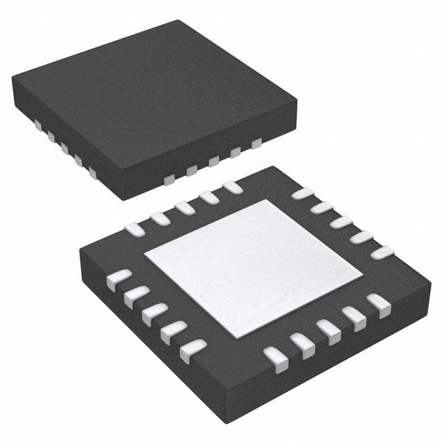


 工商网监
湘ICP备2023018690号
工商网监
湘ICP备2023018690号
