PRELIMINARY
S6E1B8 Series
32-bit ARM® Cortex®-M0+
FM0+ Microcontroller
The S6E1B8 Series is a series of highly integrated 32-bit microcontrollers designed for embedded controllers aiming at low power
consumption and low cost. This series has the ARM Cortex-M0+ Processor with on-chip Flash memory and SRAM, and consists of
peripheral functions such as various timers, LCD controller (LCDC), AES, ADC and communication interfaces (UART, CSIO (SPI),
2
2
I C, I S, Smart Card, and USB). The products which are described in this data sheet are placed into TYPE2-M0+ product categories
in "FM0+ Family Peripheral Manual".
Features
USB host
32-bit ARM Cortex-M0+ Core
USB
2.0 Full/Low-Speed supported
Interrupt-transfer and Isochronous-transfer
support
USB Device connected/disconnected automatically detect
IN/OUT token handshake packet automatically
Max 256-byte packet-length supported
Wake-up function supported
Processor version: r0p1
Bulk-transfer,
Maximum operating frequency: 40.8 MHz
Nested Vectored Interrupt Controller (NVIC): 1 NMI
(non-maskable interrupt) and 24 peripheral interrupt with 4
selectable interrupt priority levels
24-bit System timer (Sys Tick): System timer for OS task
management
LCD Controller (LCDC)
Selectable
from 44 SEG × 4 COM (Max) or 40 SEG × 8
COM (Max)
Internal Charge pump can generate 4.6 V at most
Internal divide resistor is contained (selectable from 10 k
or 100 k for the resistor value)
LCD drive power supply (bias) pin (VV4 to VV0)
Interrupt function synchronized with the LCD module frame
frequency
With blinking function
Inverted display function
Bit Band Operation
Compatible with Cortex-M3 bit band operation.
On-Chip Memory
Flash memory
Up
to 512 K+48 Kbytes
bank:
upper bank : 512 Kbytes(64 Kbytes x 8)
lower bank : 48 Kbytes(8 Kbytes x 6)
Read cycle: 0 wait-cycle
Security function for code protection
Dual
Multi-Function Serial Interface (Max 8channels)
128 bytes with Tx/Rx FIFO in all channels (The number of
FIFO steps varies depending on the settings of the
communication mode or bit length.)
SRAM
The on-chip SRAM of this series has one independent SRAM .
Up to SRAM: 60 K+4 Kbytes
4Kbytes: can retain value in Deep Standby Mode
The operation mode of each channel can be selected from
one of the following.
UART
CSIO (CSIO is known to many customers as SPI)
2
I C
USB Interface
USB interface is composed of Device and Host
PLL for USB is built-in, USB clock can be generated by
multiplication of Main clock.
UART
Full
duplex double buffer
can be enabled or disabled.
Built-in dedicated baud rate generator
External clock available as a serial clock
Various error detection functions (parity errors, framing
errors, and overrun errors)
USB Device
Parity
USB
2.0 Full-Speed supported
6 EndPoint supported
EndPoint 0 is control transfer
EndPoint 1, 2 can be selected Bulk-transfer,
Interrupt-transfer or Isochronous-transfer
EndPoint 3 to 5 can select Bulk-transfer or
Interrupt-transfer
EndPoint 1 to 5 comprise Double Buffer
The size of each EndPoint is according to the follows
EndPoint 0, 2 to 5 : 64 bytes
EndPoint 1 : 256 bytes
Max
•
•
•
•
•
•
•
Cypress Semiconductor Corporation
Document Number: 001-99223 Rev.**
•
CSIO (also known as SPI)
198 Champion Court
Full
duplex double buffer
dedicated baud rate generator
Overrun error detection function
Serial chip select function (ch1 and ch3 only)
Data length: 5 to 16 bits
Built-in
•
San Jose, CA 95134-1709
•
408-943-2600
Revised August 31, 2015
�PRELIMINARY
I2 C
Certain ports are 5 V tolerant.
Standard-mode
(Max: 100 kbps) supported / Fast-mode
(Max 400 kbps) supported.
I2 S
Using
S6E1B8 Series
2
CSIO (ch.5, ch.6) and I S clock generator
Supports two transfer protocol
2
• IS
• MSB-justified
Master mode only
Descriptor System Data Transfer Controller (DSTC)
(64 Channels)
The DSTC can transfer data at high-speed without going via
the CPU. The DSTC adopts the Descriptor
system and, following the specified contents of the
Descriptor that has already been constructed on the
memory, can access directly the memory / peripheral device
and performs the data transfer operation.
It supports the software activation, the hardware activation,
and the chain activation functions
A/D Converter (Max: 24 Channels)
12-bit A/D Converter
Successive
approximation type
time: 2.0 μs @ 2.7 V to 3.6 V
Priority conversion available (2 levels of priority)
Scan conversion mode
Built-in FIFO for conversion data storage (for scan
conversion: 16 steps, for priority conversion: 4 steps)
Conversion
Base Timer (Max: 8 Channels)
The operation mode of each channel can be selected from one
of the following.
16-bit PWM timer
16-bit PPG timer
16/32-bit reload timer
16/32-bit PWC timer
See 4. List of Pin Functions and 5. I/O Circuit Type for the
corresponding pins.
Dual Timer (32-/16-bit Down Counter)
The Dual Timer consists of two programmable 32-/16-bit down
counters. The operation mode of each timer channel can be
selected from one of the following.
Free-running mode
Periodic mode (= Reload mode)
One-shot mode
Multi-Function Timer
The Multi-function Timer consists of the following blocks.
16-bit free-run timer × 3 channels
Input capture × 4 channels
Output compare × 6 channels
ADC start compare × 6 channel
Waveform generator × 3 channels
16-bit PPG timer × 3 channels
IGBT mode is contained.
The following function can be used to achieve the motor
control.
PWM signal output function
DC chopper waveform output function
Dead time function
Input capture function
ADC start function
DTIF (motor emergency stop) interrupt function
Real-Time Clock (RTC with Vbat)
The Real-time Clock counts
year/month/day/hour/minute/second/day of the week from year
01 to year 99.
The RTC can generate an interrupt at a specific time
General-Purpose I/O Port
This series can use its pin as a general-purpose I/O port when
it is not used for an external bus or a peripheral function. All
ports can be set to fast general-purpose I/O ports or slow
general-purpose I/O ports. In addition, this series has a port
relocate function that can set to which I/O port a peripheral
function can be allocated.
All ports are Fast GPIO which can be accessed by 1cycle
Capable of controlling the pull-up of each pin
(year/month/day/hour/minute/second/day of the week) and
can also generate an interrupt in a specific year, in a specific
month, on a specific day, at a specific hour or at a specific
minute.
It has a timer interrupt function generating an interrupt upon
a specific time or at specific intervals.
It can keep counting while rewriting the time.
It can count leap years automatically.
Capable of reading pin level directly
Port relocate function
Up to 102 fast general-purpose I/O ports @120-pin package
Document Number: 001-99223 Rev.**
Page 2 of 128
�PRELIMINARY
S6E1B8 Series
Watch Counter
AES Calculator
The Watch Counter wakes up the microcontroller from the low
power consumption mode. The clock source can be selected
from the main clock, the sub clock, the built-in high-speed CR
clock or the built-in low-speed CR clock.
AES (Advanced Encryption Standard) calculator is an AES
Interval timer: up to 64 s (sub clock: 32.768 kHz)
common key crypto accelerator that is compliant with FIPS
(Federal Information Processing Standard Publication) 197.
Available key length: 128/192/256-bit
CBC mode and ECB mode support
External Interrupt Controller Unit
Up to 24 external interrupt input pins
Clock and Reset
Non-maskable interrupt (NMI) input pin: 1
Clocks
Watchdog Timer (2 Channels)
The watchdog timer generates an interrupt or a reset when the
counter reaches a time-out value.
This series consists of two different watchdogs, hardware
watchdog and software watchdog.
The hardware watchdog timer is clocked by the built-in
low-speed CR oscillator. Therefore, the hardware watchdog is
active in any low-power consumption modes except RTC, Stop,
Deep standby RTC and Deep standby Stop mode.
CRC (Cyclic Redundancy Check) Accelerator
The CRC accelerator calculates the CRC which has a heavy
software processing load, and achieves a reduction of the
integrity check processing load for reception data and storage.
CCITT CRC16 and IEEE-802.3 CRC32 are supported.
CCITT
CRC16 Generator Polynomial: 0x1021
IEEE-802.3 CRC32 Generator Polynomial: 0x04C11DB7
HDMI-CEC/Remote Control Receiver (Up to 2
Channels)
HDMI-CEC transmitter
Header
block automatic transmission by judging Signal
free
Generating status interrupt by detecting Arbitration lost
Generating START, EOM, ACK automatically to output
CEC transmission by setting 1 byte data
Generating transmission status interrupt when transmitting
1 block (1 byte data and EOM/ACK)
HDMI-CEC receiver
Automatic
ACK reply function available
Line error detection function available
Remote control receiver
4
bytes reception buffer
Repeat code detection function available
A clock can be selected from five clock sources (two external
oscillators, two built-in CR oscillator, and main PLL).
Main clock: 4 MHz to 40 MHz
Sub clock: 32.768 kHz
Built-in high-speed CR clock: 4 MHz
Built-in low-speed CR clock : 100 kHz
Main PLL clock
Resets
Reset
request from the INITX pin
on reset
Software reset
Watchdog timer reset
Low-voltage detection reset
Clock supervisor reset
Power
Clock Supervisor (CSV)
The Clock Supervisor monitors the failure of external clocks
with a clock generated by a built-in CR oscillator.
If an external clock failure (clock stop) is detected, a reset is
asserted.
If an external frequency anomaly is detected, an interrupt or
a reset is asserted.
Low-Voltage Detector (LVD)
This series monitors the voltage on the VCC pin with a 2-stage
mechanism. When the voltage falls below a designated voltage,
the Low-voltage Detector generates an interrupt or a reset.
LVDR: monitor Vcc and auto-reset operation
LVD1: monitor Vcc and error reporting via an interrupt
LVD2: selectable to monitor Vcc or LVDI and error reporting
via an interrupt
Low Power Consumption Mode
This series has six low power consumption modes.
Sleep
Smart Card Interface (Max 2 Channels)
Timer
Compliant with ISO7816-3 specification
RTC
Card Reader only/B class card only
Stop
Available protocols
Deep standby RTC (selectable between keeping the value of
Transmitter:
8E2, 8O2, 8N2
Receiver: 8E1, 8O1, 8N2, 8N1, 9N1
Inverse mode
RAM and not)
Deep standby Stop (selectable between keeping the value of
RAM and not)
TX/RX FIFO integrated (RX: 16-bytes, TX:16-bytes)
Document Number: 001-99223 Rev.**
Page 3 of 128
�PRELIMINARY
Peripheral Clock Gating
Power Supply
The system can reduce the current consumption of the total
system with gating the operation clocks of peripheral functions
not used.
Wide voltage range:
VBAT
The consumption power during the RTC operation can be
reduced by supplying the power supply independent VBAT pin.
RTC (calendar circuit) / 32 kHz oscillation circuit. The following
circuit can also be used.
S6E1B8 Series
VCC = 1.65V to 3.6 V
VCC = 3.0V to 3.6V (when USB is used)
VCC = 2.2V to 3.6V (when LCDC is used)
Power supply for VBAT: VBAT = 1.65 V to 3.6 V
RTC
32 kHz oscillation circuit
Power-on circuit
Back up register: 32 bytes
Port circuit
Debug
Serial Wire Debug Port (SW-DP)
Micro Trace Buffer (MTB)
Unique ID
A 41-bit unique value of the device has been set.
Document Number: 001-99223 Rev.**
Page 4 of 128
�PRELIMINARY
S6E1B8 Series
Table of Contents
Features................................................................................................................................................................................... 1
1.
Product Lineup ............................................................................................................................................................... 7
2.
Packages......................................................................................................................................................................... 8
3.
Pin Assignment .............................................................................................................................................................. 9
4.
List of Pin Functions .................................................................................................................................................... 12
5.
I/O Circuit Type ............................................................................................................................................................. 36
6.
Handling Precautions .................................................................................................................................................. 46
6.1
Precautions for Product Design ................................................................................................................................... 46
6.2
Precautions for Package Mounting .............................................................................................................................. 47
6.3
Precautions for Use Environment ................................................................................................................................ 49
7.
Handling Devices ......................................................................................................................................................... 50
8.
Block Diagram .............................................................................................................................................................. 53
9.
Memory Map ................................................................................................................................................................. 54
10. Pin Status in Each CPU State ...................................................................................................................................... 57
11. Electrical Characteristics ............................................................................................................................................ 67
11.1 Absolute Maximum Ratings ......................................................................................................................................... 67
11.2 Recommended Operating Conditions.......................................................................................................................... 68
11.3 DC Characteristics....................................................................................................................................................... 69
11.3.1 Current Rating .............................................................................................................................................................. 69
11.3.2 Pin Characteristics ....................................................................................................................................................... 74
11.3.3 LCD Characteristic ....................................................................................................................................................... 75
11.4 AC Characteristics ....................................................................................................................................................... 79
11.4.1 Main Clock Input Characteristics .................................................................................................................................. 79
11.4.2 Sub Clock Input Characteristics ................................................................................................................................... 80
11.4.3 Built-in CR Oscillation Characteristics .......................................................................................................................... 81
11.4.4 Operating Conditions of Main PLL (In the Case of Using the Main Clock as the Input Clock of the PLL) .................... 82
11.4.5 Operating Conditions of Main PLL (In the Case of Using the Built-in High-Speed CR Clock as the
Input Clock of the Main PLL) ........................................................................................................................................ 82
11.4.6 Reset Input Characteristics .......................................................................................................................................... 83
11.4.7 Power-on Reset Timing................................................................................................................................................ 83
11.4.8 Base Timer Input Timing .............................................................................................................................................. 84
11.4.9 CSIO/SPI/UART Timing ............................................................................................................................................... 85
11.4.10 External Input Timing .............................................................................................................................................. 102
2
11.4.11 I C Timing ............................................................................................................................................................... 103
2
11.4.12 I S Timing ............................................................................................................................................................... 104
11.4.13 Smart Card Interface Characteristics ...................................................................................................................... 105
11.4.14 SW-DP Timing ........................................................................................................................................................ 106
11.5 12-bit A/D Converter .................................................................................................................................................. 107
11.6 USB Characteristics .................................................................................................................................................. 110
11.7 Low-Voltage Detection Characteristics ...................................................................................................................... 115
11.7.1 Low-Voltage Detection Reset ..................................................................................................................................... 115
11.7.2 Low-Voltage Detection Interrupt ................................................................................................................................. 116
11.7.3 Low-Voltage Detection Interrupt 2 .............................................................................................................................. 117
11.8 Flash Memory Write/Erase Characteristics ............................................................................................................... 118
11.9 Return Time from Low-Power Consumption Mode .................................................................................................... 119
11.9.1 Return Factor: Interrupt/WKUP .................................................................................................................................. 119
11.9.2 Return Factor: Reset .................................................................................................................................................. 121
12. Ordering Information ................................................................................................................................................. 123
Document Number: 001-99223 Rev.**
Page 5 of 128
�PRELIMINARY
S6E1B8 Series
13. Package Dimensions ................................................................................................................................................. 124
Document History ............................................................................................................................................................... 127
Sales, Solutions, and Legal Information........................................................................................................................... 128
Document Number: 001-99223 Rev.**
Page 6 of 128
�PRELIMINARY
S6E1B8 Series
1. Product Lineup
Memory Size
Product Name
Upper Bank
On-chip Flash memory
Lower Bank
On-chip SRAM
S6E1B84E/F/G
256 Kbytes
48 Kbytes
32 Kbytes
S6E1B86E/F/G
512 Kbytes
48 Kbytes
64 Kbytes
Function
S6E1B84E0A
S6E1B86E0A
S6E1B84EHA
S6E1B86EHA
80
Product Name
Pin count
S6E1B84F0A
S6E1B86F0A
S6E1B84FHA
S6E1B86FHA
100
Cortex-M0+
40.8 MHz
1.65 V to 3.6 V
1 unit
64ch
8ch (Max) with 128 bytes FIFO
2
I S: ch.5, ch.6
CPU
Frequency
Power supply voltage range
USB 2.0 (Device/Host)
DSTC
Multi-function Serial Interface
2
2
(UART/CSIO (SPI)/I C/I S)
Base Timer
(PWC/Reload timer/PWM/PPG)
8ch (Max)
20SEG x 8COM(Max) /
24SEG x 4COM(Max)
Multi-function
Timer
LCD controller
A/D activation
compare
Input capture
Free-run timer
Output compare
Waveform generator
PPG
32SEG x 8COM(Max) /
36SEG x 4COM(Max)
40SEG x 8COM(Max) /
44SEG x 4COM(Max)
6ch
4ch
3ch
6ch
3ch
3ch
1 unit
Dual Timer
1 unit
HDMI-CEC/ Remote Control Receiver
Smart Card Interface
Real-time Clock
Watch Counter
CRC Accelerator
Watchdog timer
External Interrupt
I/O port
12-bit A/D converter
CSV (Clock Supervisor)
LVD (Low-voltage Detection)
High-speed
Built-in CR
Low-speed
Debug Function
Unique ID
AES Calculator
S6E1B84G0A
S6E1B86G0A
S6E1B84GHA
S6E1B86GHA
120
2ch (max)
65 pins (Max)
16ch (1 unit)
-
Yes
*1
2ch (max)
1 unit (with battery power)
1 unit
Yes
1ch (SW) + 1ch (HW)
24 pins (Max), NMI × 1
82 pins (Max)
23ch (1 unit)
Yes
2ch
4 MHz
100 kHz
SW-DP
Yes
*1
Yes
102 pins (Max)
24ch (1 unit)
-
Yes
*1
*1: AES Calculator is built in following products.
S6E1B86GHA, S6E1B84GHA, S6E1B86FHA, S6E1B84FHA, S6E1B86EHA, S6E1B84EHA
Note:
−
All signals of the peripheral function in each product cannot be allocated by limiting the pins of package. It is necessary to use
the port relocate function of the I/O port according to your function use.
See "11 Electrical Characteristics 11.4 AC Characteristics 11.4.3 Built-in CR Oscillation Characteristics" for accuracy of built-in
CR.
Document Number: 001-99223 Rev.**
Page 7 of 128
�PRELIMINARY
S6E1B8 Series
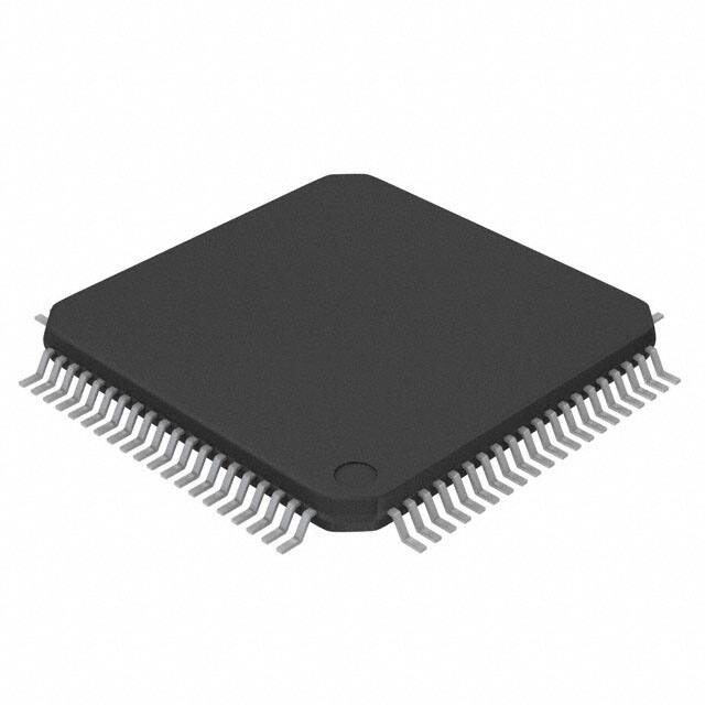
2. Packages
Product Name
Package
LQFP:
FPT-80P-M21 (0.50
mm pitch)
LQFP:
FPT-100P-M20
(0.50 mm pitch)
LQFP:
FPT-120P-M21
(0.50 mm pitch)
: Available
S6E1B84E/S6E1B86E
S6E1B84F/S6E1B86F
S6E1B84G/S6E1B86G
-
-
-
-
-
-
Note:
−
See "13. Package Dimensions" for detailed information on each package.
Document Number: 001-99223 Rev.**
Page 8 of 128
�PRELIMINARY
S6E1B8 Series
3. Pin Assignment
FPT-80P-M21
61 P00/SOT3_2/INT14_1
62 P01/SWCLK
63 P02/SIN3_2/TIOB5_0
64 P03/SWDIO
65 P04/SCK3_2/INT06_2
66 P07/AN22/ADTG_0/SCK4_2/INT23_1/SEG07/SOT4_0
67 P0A/SIN4_0/INT00_2/WKUP5/IC0_CIN_0/UHCONX0/CEC0_1
68 P0B/INT18_0/UDM0
69 P0C/INT19_0/UDP0
70 P0D/RTS4_0/TIOA3_2/INT20_0/SEG04/IC0_VPEN_0
71 P0E/CTS4_0/TIOB3_2/INT21_0/SEG03/IC0_VCC_0
72 P0F/NMIX/CROUT_1/RTCCO_0/SUBOUT_0/MI2SMCK5_0/WKUP0/IC0_CLK_0/SCK4_0
73 P63/MI2SWS5_0/INT03_0/SEG02/TIOB6_1/IC0_DATA_0
74 P62/SCK5_0/MI2SCK5_0/ADTG_3/INT07_1/SEG01/TIOA6_1/IC0_RST_0
75 P61/SOT5_0/MI2SDO5_0/TIOB2_2/DTTI0X_2/SEG00
76 P60/SIN5_0/MI2SDI5_0/TIOA2_2/INT15_1/WKUP3/CEC1_0/IGTRG0_1
77 P80/SIN7_2/INT20_1/C0
78 P81/SOT7_2/INT11_0/C1
79 P82/SCK7_2
80 VSS
(TOP VIEW)
VCC
1
60 P21/AN18/SIN0_0/INT06_1/WKUP2/SEG11
P50/INT00_0/SIN3_1/VV4
2
59 P22/AN17/SOT0_0/TIOB7_1/SEG12
P51/INT01_0/SOT3_1/VV3
3
58 P23/AN16/SCK0_0/TIOA7_1/RTO00_1/SEG13
P52/INT02_0/SCK3_1/VV2
4
57 P1B/AN11/SOT4_1/IC02_1/INT20_2/SEG16
P53/SIN6_0/TIOA1_2/INT07_2/VV1
5
P54/SOT6_0/TIOB1_2/INT18_1/VV0
6
P55/SCK6_0/ADTG_1/INT19_1/SEG39
7
P56/INT08_2/MI2SMCK6_1/SEG38/WKUP9/CEC1_1
8
P30/TIOB0_1/SCS60_1/INT03_2/MI2SWS6_1/COM7/SEG43/WKUP4
9
P31/TIOB1_1/SCK6_1/MI2SCK6_1/INT04_2/COM6/SEG42
10
P32/TIOB2_1/SOT6_1/MI2SDO6_1/INT05_2/COM5/SEG41
11
P33/INT04_0/TIOB3_1/SIN6_1/MI2SDI6_1/ADTG_6/COM4/SEG40
12
49 P17/AN07/SIN2_2/INT04_1/SEG20
P39/DTTI0X_0/ADTG_2/TIOB4_0/INT06_0/COM3
13
48 P16/AN06/SCK0_1/INT15_0/SEG21
P3A/RTO00_0/TIOA0_1/INT07_0/RTCCO_2/SUBOUT_2/IC1_CIN_0/COM2
14
47 P15/AN05/IC1_CIN_1/SOT0_1/IC03_2/INT14_0/SEG22
P3B/RTO01_0/TIOA1_1/IC1_DATA_0/COM1
15
46 P14/AN04/IC1_DATA_1/RTS1_1/SIN0_1/INT03_1/IC02_2/SEG23
P3C/RTO02_0/TIOA2_1/INT18_2/IC1_RST_0/COM0
16
45 P13/AN03/IC1_RST_1/SCK1_1/RTCCO_1/IC01_2/SUBOUT_1/SEG24
P3D/RTO03_0/TIOA3_1/IC1_VPEN_0/SEG36
17
44 P12/AN02/IC1_VPEN_1/SOT1_1/IC00_2/SEG25
P3E/RTO04_0/TIOA4_1/INT19_2/IC1_VCC_0/SEG35/WKUP8
18
43 P11/AN01/IC1_VCC_1/SIN1_1/INT02_1/FRCK0_2/WKUP1/SEG26
P3F/RTO05_0/TIOA5_1/IC1_CLK_0/SEG34
19
42 P10/AN00/IC1_CLK_1/CTS1_1/SEG27
56 P1A/AN10/SIN4_1/IC01_1/INT05_1/SEG17
LQFP - 100
55 P19/AN09/SCK2_2/IC00_1/SEG18
`
54 P18/AN08/SOT2_2/SEG19
53 AVRH
52 AVRL
51 AVSS
LQFP - 80
50 AVCC
VSS 40
PE3/X1 39
PE2/X0 38
35
P4D/TIOB3_0/INT13_0/SCK7_1/WKUP6/SEG28
MD0 37
34
P4C/TIOB2_0/SOT7_1/INT12_0/SEG29/CEC0_0
PE0/MD1 36
33
P4B/TIOB1_0/SIN7_1/INT22_1/WKUP7/SEG30/IGTRG0_0
P4A/TIOB0_0/SCS70_1/INT21_1/SEG31 32
VBAT 31
P49/VWAKEUP 30
P48/VREGCTL 29
P47/X1A 28
P46/X0A 27
26
INITX
VCC 25
VSS 24
23
C
P45/LVDI/TIOA5_0/SEG32/IC0_CIN_1 22
41 VCC
P44/TIOA4_0/INT10_0/SEG33/RTS1_2/IC0_DATA_1 21
VSS 20
Note:
−
The number after the underscore ("_") in a pin name such as XXX_1 and XXX_2 indicates the relocated port number. The
channel on such pin has multiple functions, each of which has its own pin name. Use the Extended Port Function Register
(EPFR) to select the pin to be used.
Document Number: 001-99223 Rev.**
Page 9 of 128
�PRELIMINARY
S6E1B8 Series
FPT-100P-M20
P82/SCK7_2
P81/SOT7_2/INT11_0/C1
P80/SIN7_2/INT20_1/C0
P60/SIN5_0/MI2SDI5_0/TIOA2_2/INT15_1/WKUP3/CEC1_0/IGTRG0_1
P61/SOT5_0/MI2SDO5_0/TIOB2_2/DTTI0X_2/SEG00
P62/SCK5_0/MI2SCK5_0/ADTG_3/INT07_1/SEG01/TIOA6_1/IC0_RST_0
P63/MI2SWS5_0/INT03_0/SEG02/TIOB6_1/IC0_DATA_0
P0F/NMIX/CROUT_1/RTCCO_0/SUBOUT_0/MI2SMCK5_0/WKUP0/IC0_CLK_0/SCK4_0
P0E/CTS4_0/TIOB3_2/INT21_0/SEG03/IC0_VCC_0
P0D/RTS4_0/TIOA3_2/INT20_0/SEG04/IC0_VPEN_0
P0C/INT19_0/UDP0
P0B/INT18_0/UDM0
P0A/SIN4_0/INT00_2/WKUP5/IC0_CIN_0/UHCONX0/CEC0_1
P09/TIOB0_2/RTS4_2/INT17_0/SEG05
P08/AN23/TIOA0_2/CTS4_2/INT16_0/SEG06
P07/AN22/ADTG_0/SCK4_2/INT23_1/SEG07/SOT4_0
P06/AN21/TIOB5_2/SOT4_2/INT01_1/SEG08
P05/AN20/TIOA5_2/SIN4_2/INT00_1/SEG09/WKUP10
P04/SCK3_2/INT06_2
P03/SWDIO
P02/SIN3_2/TIOB5_0
P01/SWCLK
P00/SOT3_2/INT14_1
VCC
99
98
97
96
95
94
93
92
91
90
89
88
87
86
85
84
83
82
81
80
79
78
77
76
100 VSS
(TOP VIEW)
VCC
1
75 VSS
P50/INT00_0/SIN3_1/VV4
2
74 P20/AN19/INT05_0/CROUT_0/SEG10
P51/INT01_0/SOT3_1/VV3
3
73 P21/AN18/SIN0_0/INT06_1/WKUP2/SEG11
72 P22/AN17/SOT0_0/TIOB7_1/SEG12
P52/INT02_0/SCK3_1/VV2
4
P53/SIN6_0/TIOA1_2/INT07_2/VV1
5
P54/SOT6_0/TIOB1_2/INT18_1/VV0
6
P55/SCK6_0/ADTG_1/INT19_1/SEG39
7
69 P1D/AN13/CTS4_1/DTTI0X_1/INT22_2/SEG14
P56/INT08_2/MI2SMCK6_1/SEG38/WKUP9/CEC1_1
8
68 P1C/AN12/SCK4_1/IC03_1/INT21_2/SEG15
P30/TIOB0_1/SCS60_1/INT03_2/MI2SWS6_1/COM7/SEG43/WKUP4
9
67 P1B/AN11/SOT4_1/IC02_1/INT20_2/SEG16
71 P23/AN16/SCK0_0/TIOA7_1/RTO00_1/SEG13
LQFP - 100
70 P1E/AN14/RTS4_1/ADTG_5/FRCK0_1/INT23_2
P31/TIOB1_1/SCK6_1/MI2SCK6_1/INT04_2/COM6/SEG42 10
66 P1A/AN10/SIN4_1/IC01_1/INT05_1/SEG17
P32/TIOB2_1/SOT6_1/MI2SDO6_1/INT05_2/COM5/SEG41 11
65 P19/AN09/SCK2_2/IC00_1/SEG18
P33/INT04_0/TIOB3_1/SIN6_1/MI2SDI6_1/ADTG_6/COM4/SEG40 12
64 P18/AN08/SOT2_2/SEG19
LQFP - 100
P34/SCS61_1/FRCK0_0/TIOB4_1 13
63 AVRH
P35/SCS62_1/IC03_0/TIOB5_1/INT08_1/SEG37 14
62 AVRL
P36/IC02_0/SIN5_2/INT09_1/WKUP11 15
61 AVSS
P37/IC01_0/SOT5_2/INT10_1 16
60 AVCC
P38/IC00_0/SCK5_2/INT11_1 17
59 P17/AN07/SIN2_2/INT04_1/SEG20
P39/DTTI0X_0/ADTG_2/TIOB4_0/INT06_0/COM3 18
58 P16/AN06/SCK0_1/INT15_0/SEG21
P3A/RTO00_0/TIOA0_1/INT07_0/RTCCO_2/SUBOUT_2/IC1_CIN_0/COM2 19
57 P15/AN05/IC1_CIN_1/SOT0_1/IC03_2/INT14_0/SEG22
P3B/RTO01_0/TIOA1_1/IC1_DATA_0/COM1 20
56 P14/AN04/IC1_DATA_1/RTS1_1/SIN0_1/INT03_1/IC02_2/SEG23
P3C/RTO02_0/TIOA2_1/INT18_2/IC1_RST_0/COM0 21
55 P13/AN03/IC1_RST_1/SCK1_1/RTCCO_1/IC01_2/SUBOUT_1/SEG24
P3D/RTO03_0/TIOA3_1/IC1_VPEN_0/SEG36 22
54 P12/AN02/IC1_VPEN_1/SOT1_1/IC00_2/SEG25
P3E/RTO04_0/TIOA4_1/INT19_2/IC1_VCC_0/SEG35/WKUP8 23
53 P11/AN01/IC1_VCC_1/SIN1_1/INT02_1/FRCK0_2/WKUP1/SEG26
P3F/RTO05_0/TIOA5_1/IC1_CLK_0/SEG34 24
52 P10/AN00/IC1_CLK_1/CTS1_1/SEG27
VSS 50
PE3/X1 49
PE2/X0 48
45
P4D/TIOB3_0/INT13_0/SCK7_1/WKUP6/SEG28
MD0 47
44
P4C/TIOB2_0/SOT7_1/INT12_0/SEG29/CEC0_0
PE0/MD1 46
43
P4B/TIOB1_0/SIN7_1/INT22_1/WKUP7/SEG30/IGTRG0_0
P4A/TIOB0_0/SCS70_1/INT21_1/SEG31 42
VBAT 41
P49/VWAKEUP 40
P48/VREGCTL 39
P47/X1A 38
P46/X0A 37
36
VCC 35
INITX
VSS 34
33
C
P45/LVDI/TIOA5_0/SEG32/IC0_CIN_1 32
P44/TIOA4_0/INT10_0/SEG33/RTS1_2/IC0_DATA_1 31
30
P43/TIOA3_0/INT09_0/ADTG_7/CTS1_2/IC0_RST_1
P42/TIOA2_0/INT08_0/SCK1_2/IC0_VPEN_1 29
P41/TIOA1_0/INT13_1/SOT1_2/IC0_VCC_1 28
VCC 26
51 VCC
P40/TIOA0_0/INT12_1/SIN1_2/IC0_CLK_1 27
VSS 25
Note:
−
The number after the underscore ("_") in a pin name such as XXX_1 and XXX_2 indicates the relocated port number. The
channel on such pin has multiple functions, each of which has its own pin name. Use the Extended Port Function Register
(EPFR) to select the pin to be used.
Document Number: 001-99223 Rev.**
Page 10 of 128
�PRELIMINARY
S6E1B8 Series
FPT-120P-M21
P07/AN22/ADTG_0/SCK4_2/INT23_1/SEG07/SOT4_0
P06/AN21/TIOB5_2/SOT4_2/INT01_1/SEG08
P05/AN20/TIOA5_2/SIN4_2/INT00_1/SEG09/WKUP10
P04/SCK3_2/INT06_2
P03/SWDIO
P02/SIN3_2/TIOB5_0
P01/SWCLK
P00/SOT3_2/INT14_1
VCC
99
98
97
96
95
94
93
92
91
100 P08/AN23/TIOA0_2/CTS4_2/INT16_0/SEG06
101 P09/TIOB0_2/RTS4_2/INT17_0/SEG05
102 P0A/SIN4_0/INT00_2/WKUP5/IC0_CIN_0/UHCONX0/CEC0_1
103 P0B/INT18_0/UDM0
104 P0C/INT19_0/UDP0
105 P0D/RTS4_0/TIOA3_2/INT20_0/SEG04/IC0_VPEN_0
106 P0E/CTS4_0/TIOB3_2/INT21_0/SEG03/IC0_VCC_0
107 P0F/NMIX/CROUT_1/RTCCO_0/SUBOUT_0/MI2SMCK5_0/WKUP0/IC0_CLK_0/SCK4_0
108 P68/SCK3_0/TIOB7_2/INT12_2
109 P67/SOT3_0/TIOA7_2/INT22_0
110 P66/SIN3_0/INT11_2
111 P65/SCK5_1/TIOB7_0/INT23_0
112 P64/SOT5_1/TIOA7_0/INT10_2
113 P63/SIN5_1/MI2SWS5_0/INT03_0/SEG02/TIOB6_1/IC0_DATA_0
114 P62/SCK5_0/MI2SCK5_0/ADTG_3/INT07_1/SEG01/TIOA6_1/IC0_RST_0
115 P61/SOT5_0/MI2SDO5_0/TIOB2_2/DTTI0X_2/SEG00
116 P60/SIN5_0/MI2SDI5_0/TIOA2_2/INT15_1/WKUP3/CEC1_0/IGTRG0_1
117 P80/SIN7_2/INT20_1/C0
118 P81/SOT7_2/INT11_0/C1
119 P82/SCK7_2
120 VSS
(TOP VIEW)
VCC
1
90
VSS
P50/INT00_0/SIN3_1/VV4
2
89
P20/AN19/INT05_0/CROUT_0/SEG10
P51/INT01_0/SOT3_1/VV3
3
88
P21/AN18/SIN0_0/INT06_1/WKUP2/SEG11
P52/INT02_0/SCK3_1/VV2
4
87
P22/AN17/SOT0_0/TIOB7_1/SEG12
P53/SIN6_0/TIOA1_2/INT07_2/VV1
5
86
P23/AN16/SCK0_0/TIOA7_1/RTO00_1/SEG13
P54/SOT6_0/TIOB1_2/INT18_1/VV0
6
85
P24/SIN2_1/RTO01_1/INT17_1
P55/SCK6_0/ADTG_1/INT19_1/SEG39
7
84
P25/SOT2_1/RTO02_1
P56/SIN1_0/INT08_2/MI2SMCK6_1/SEG38/WKUP9/CEC1_1
8
83
P26/SCK2_1/RTO03_1
P57/SOT1_0
9
82
P27/AN15/RTO04_1/TIOA6_2/INT02_2
P58/SCK1_0
10
81
P28/ADTG_4/RTO05_1/TIOB6_2
P59/SIN7_0/INT16_1
11
80
P1E/AN14/RTS4_1/ADTG_5/FRCK0_1/INT23_2
P5A/SOT7_0/INT16_2
12
79
P1D/AN13/CTS4_1/DTTI0X_1/INT22_2/SEG14
P5B/SCK7_0/INT17_2
13
78
P1C/AN12/SCK4_1/IC03_1/INT21_2/SEG15
P30/TIOB0_1/SCS60_1/INT03_2/MI2SWS6_1/COM7/SEG43/WKUP4
14
77
P1B/AN11/SOT4_1/IC02_1/INT20_2/SEG16
P31/TIOB1_1/SCK6_1/MI2SCK6_1/INT04_2/COM6/SEG42
15
76
P1A/AN10/SIN4_1/IC01_1/INT05_1/SEG17
P32/TIOB2_1/SOT6_1/MI2SDO6_1/INT05_2/COM5/SEG41
16
75
P19/AN09/SCK2_2/IC00_1/SEG18
P33/INT04_0/TIOB3_1/SIN6_1/MI2SDI6_1/ADTG_6/COM4/SEG40
17
74
P18/AN08/SOT2_2/SEG19
P34/SCS61_1/FRCK0_0/TIOB4_1
18
73
AVRH
P35/SCS62_1/IC03_0/TIOB5_1/INT08_1/SEG37
19
72
AVRL
P36/IC02_0/SIN5_2/INT09_1/WKUP11
20
71
AVSS
P37/IC01_0/SOT5_2/INT10_1
21
70
AVCC
P38/IC00_0/SCK5_2/INT11_1
22
69
P17/AN07/SIN2_2/INT04_1/SEG20
P39/DTTI0X_0/ADTG_2/TIOB4_0/INT06_0/COM3
23
68
P16/AN06/SCK0_1/INT15_0/SEG21
P3A/RTO00_0/TIOA0_1/INT07_0/RTCCO_2/SUBOUT_2/IC1_CIN_0/COM2
24
67
P15/AN05/IC1_CIN_1/SOT0_1/IC03_2/INT14_0/SEG22
LQFP - 120
40
41
42
43
44
45
46
47
48
49
50
51
52
53
54
55
56
57
58
59
60
INITX
P46/X0A
P47/X1A
P48/VREGCTL
P49/VWAKEUP
VBAT
P4A/TIOB0_0/SCS70_1/INT21_1/SEG31
P4B/TIOB1_0/SIN7_1/INT22_1/WKUP7/SEG30/IGTRG0_0
P4C/TIOB2_0/SOT7_1/INT12_0/SEG29/CEC0_0
P4D/TIOB3_0/INT13_0/SCK7_1/WKUP6/SEG28
P70/SCS71_1/TIOA4_2
P71/SCS72_1/TIOB4_2/INT13_2
P72/SIN2_0/TIOA6_0/INT14_2
P73/SOT2_0/TIOB6_0/INT15_2
P74/SCK2_0
PE0/MD1
MD0
PE2/X0
PE3/X1
VSS
VCC
VCC
VCC
39
61
VSS
30
38
P10/AN00/IC1_CLK_1/CTS1_1/SEG27
VSS
C
62
37
29
P45/LVDI/TIOA5_0/SEG32/IC0_CIN_1
P11/AN01/IC1_VCC_1/SIN1_1/INT02_1/FRCK0_2/WKUP1/SEG26
P3F/RTO05_0/TIOA5_1/IC1_CLK_0/SEG34
P44/TIOA4_0/INT10_0/SEG33/RTS1_2/IC0_DATA_1 36
63
35
28
P43/TIOA3_0/INT09_0/ADTG_7/CTS1_2/IC0_RST_1
P12/AN02/IC1_VPEN_1/SOT1_1/IC00_2/SEG25
P3E/RTO04_0/TIOA4_1/INT19_2/IC1_VCC_0/SEG35/WKUP8
34
64
P42/TIOA2_0/INT08_0/SCK1_2/IC0_VPEN_1
27
33
P13/AN03/IC1_RST_1/SCK1_1/RTCCO_1/IC01_2/SUBOUT_1/SEG24
P3D/RTO03_0/TIOA3_1/IC1_VPEN_0/SEG36
32
P14/AN04/IC1_DATA_1/RTS1_1/SIN0_1/INT03_1/IC02_2/SEG23
65
31
66
26
P40/TIOA0_0/INT12_1/SIN1_2/IC0_CLK_1
25
P41/TIOA1_0/INT13_1/SOT1_2/IC0_VCC_1
P3B/RTO01_0/TIOA1_1/IC1_DATA_0/COM1
P3C/RTO02_0/TIOA2_1/INT18_2/IC1_RST_0/COM0
Note:
−
The number after the underscore ("_") in a pin name such as XXX_1 and XXX_2 indicates the relocated port number. The
channel on such pin has multiple functions, each of which has its own pin name. Use the Extended Port Function Register
(EPFR) to select the pin to be used.
Document Number: 001-99223 Rev.**
Page 11 of 128
�PRELIMINARY
S6E1B8 Series
4. List of Pin Functions
List of Pin Numbers
The number after the underscore ("_") in a pin name such as XXX_1 and XXX_2 indicates the relocated port number. The channel
on such pin has multiple functions, each of which has its own pin name. Use the Extended Port Function Register (EPFR) to select
the pin to be used.
Pin No.
LQFP-120
LQFP-100
LQFP-80
1
1
1
Pin Name
I/O Circuit Type
VCC
Pin State Type
-
P50
SIN3_1
2
2
2
Q
X
Q
X
Q
X
Q
X
Q
X
L
S
L
U
F
I
F
I
F
J
INT00_0
VV4
3
3
3
4
4
4
5
5
5
6
6
6
7
7
7
P51
SOT3_1
INT01_0
VV3
P52
SCK3_1
INT02_0
VV2
P53
SIN6_0
TIOA1_2
INT07_2
VV1
P54
SOT6_0
TIOB1_2
INT18_1
VV0
P55
SCK6_0
ADTG_1
INT19_1
8
8
-
-
9
-
-
10
-
-
11
-
-
8
Document Number: 001-99223 Rev.**
SEG39
P56
MI2SMCK6_1
CEC1_1
INT08_2
WKUP9
SEG38
SIN1_0
P57
SOT1_0
P58
SCK1_0
P59
SIN7_0
INT16_1
Page 12 of 128
�PRELIMINARY
Pin No.
LQFP-120
LQFP-100
LQFP-80
12
-
-
13
-
-
14
9
9
15
10
10
16
11
11
17
12
12
18
13
-
19
14
-
20
15
-
21
16
-
Document Number: 001-99223 Rev.**
Pin Name
P5A
SOT7_0
INT16_2
P5B
SCK7_0
INT17_2
P30
TIOB0_1
SCS60_1
MI2SWS6_1
INT03_2
WKUP4
COM7
SEG43
P31
TIOB1_1
SCK6_1
MI2SCK6_1
INT04_2
COM6
SEG42
P32
TIOB2_1
SOT6_1
MI2SDO6_1
INT05_2
COM5
SEG41
P33
TIOB3_1
SIN6_1
MI2SDI6_1
INT04_0
ADTG_6
COM4
SEG40
P34
SCS61_1
FRCK0_0
TIOB4_1
P35
SCS62_1
IC03_0
TIOB5_1
INT08_1
SEG37
P36
IC02_0
SIN5_2
INT09_1
WKUP11
P37
IC01_0
SOT5_2
INT10_1
S6E1B8 Series
I/O Circuit Type
Pin State Type
F
J
F
J
M
T
M
S
M
S
M
S
I
I
L
S
I
N
I
J
Page 13 of 128
�PRELIMINARY
Pin No.
LQFP-120
LQFP-100
LQFP-80
22
17
-
23
18
13
24
19
14
25
20
15
26
21
16
27
22
17
28
23
18
29
24
19
30
31
25
26
20
-
32
27
-
Document Number: 001-99223 Rev.**
Pin Name
P38
IC00_0
SCK5_2
INT11_1
P39
DTTI0X_0
TIOB4_0
ADTG_2
INT06_0
COM3
P3A
RTO00_0
TIOA0_1
RTCCO_2
SUBOUT_2
IC1_CIN_0
INT07_0
COM2
P3B
RTO01_0
TIOA1_1
IC1_DATA_0
COM1
P3C
RTO02_0
TIOA2_1
INT18_2
IC1_RST_0
COM0
P3D
RTO03_0
TIOA3_1
IC1_VPEN_0
SEG36
P3E
RTO04_0
TIOA4_1
IC1_VCC_0
INT19_2
WKUP8
SEG35
P3F
RTO05_0
TIOA5_1
IC1_CLK_0
SEG34
VSS
VCC
P40
TIOA0_0
IC0_CLK_1
INT12_1
SIN1_2
S6E1B8 Series
I/O Circuit Type
Pin State Type
F
J
N
S
N
S
N
P
N
S
L
P
L
T
L
P
-
-
F
J
Page 14 of 128
�PRELIMINARY
Pin No.
LQFP-120
LQFP-100
LQFP-80
33
28
-
34
29
-
35
30
-
36
31
21
37
32
22
38
39
40
41
33
34
35
36
23
24
25
26
42
37
27
43
38
28
44
39
29
45
40
30
46
41
31
47
42
32
48
43
33
Document Number: 001-99223 Rev.**
Pin Name
P41
TIOA1_0
SOT1_2
IC0_VCC_1
INT13_1
P42
TIOA2_0
SCK1_2
IC0_VPEN_1
INT08_0
P43
TIOA3_0
CTS1_2
ADTG_7
IC0_RST_1
INT09_0
P44
TIOA4_0
IC0_DATA_1
INT10_0
RTS1_2
SEG33
P45
TIOA5_0
IC0_CIN_1
LVDI
SEG32
C
VSS
VCC
INITX
P46
X0A
P47
X1A
P48
VREGCTL
P49
VWAKEUP
VBAT
P4A
TIOB0_0
SCS70_1
INT21_1
SEG31
P4B
TIOB1_0
SIN7_1
INT22_1
WKUP7
SEG30
IGTRG0_0
S6E1B8 Series
I/O Circuit Type
Pin State Type
F
J
F
J
F
J
L
S
L
P
B
C
D
E
E
F
I
I
I
I
-
-
L
S
L
T
Page 15 of 128
�PRELIMINARY
Pin No.
LQFP-120
LQFP-100
LQFP-80
Pin Name
P4C
TIOB2_0
SOT7_1
CEC0_0
INT12_0
SEG29
P4D
TIOB3_0
SCK7_1
INT13_0
WKUP6
SEG28
P70
TIOA4_2
SCS71_1
P71
TIOB4_2
SCS72_1
INT13_2
P72
SIN2_0
TIOA6_0
INT14_2
P73
SOT2_0
TIOB6_0
INT15_2
P74
SCK2_0
PE0
MD1
MD0
PE2
X0
PE3
S6E1B8 Series
I/O Circuit Type
Pin State Type
L
R
L
T
F
I
F
J
F
J
F
J
F
I
C
D
J
M
A
A
A
B
49
44
34
50
45
35
51
-
-
52
-
-
53
-
-
54
-
-
55
-
-
56
46
36
57
47
37
58
48
38
59
49
39
60
50
40
VSS
-
-
61
51
41
VCC
-
-
P
K
P
W
62
52
42
63
53
43
Document Number: 001-99223 Rev.**
X1
P10
IC1_CLK_1
CTS1_1
AN00
SEG27
P11
IC1_VCC_1
SIN1_1
FRCK0_2
INT02_1
WKUP1
AN01
SEG26
Page 16 of 128
�PRELIMINARY
Pin No.
LQFP-120
LQFP-100
LQFP-80
64
54
44
65
55
45
66
56
46
67
57
47
68
58
48
69
59
49
70
71
72
73
60
61
62
63
50
51
52
53
74
64
54
75
65
55
Document Number: 001-99223 Rev.**
Pin Name
P12
IC1_VPEN_1
SOT1_1
IC00_2
AN02
SEG25
P13
IC1_RST_1
SCK1_1
RTCCO_1
IC01_2
SUBOUT_1
AN03
SEG24
P14
IC1_DATA_1
RTS1_1
SIN0_1
IC02_2
INT03_1
AN04
SEG23
P15
IC1_CIN_1
SOT0_1
IC03_2
INT14_0
AN05
SEG22
P16
SCK0_1
INT15_0
AN06
SEG21
P17
SIN2_2
INT04_1
AN07
SEG20
AVCC
AVSS
AVRL
AVRH
P18
SOT2_2
AN08
SEG19
P19
SCK2_2
IC00_1
AN09
SEG18
S6E1B8 Series
I/O Circuit Type
Pin State Type
P
K
P
K
P
V
P
V
P
V
P
V
-
-
P
K
P
K
Page 17 of 128
�PRELIMINARY
Pin No.
LQFP-120
LQFP-100
LQFP-80
76
66
56
77
67
57
78
68
-
79
69
-
80
70
-
81
-
-
82
-
-
83
-
-
84
-
-
85
-
-
86
71
58
Document Number: 001-99223 Rev.**
Pin Name
P1A
SIN4_1
IC01_1
INT05_1
AN10
SEG17
P1B
SOT4_1
IC02_1
INT20_2
AN11
SEG16
P1C
SCK4_1
IC03_1
INT21_2
AN12
SEG15
P1D
CTS4_1
DTTI0X_1
INT22_2
AN13
SEG14
P1E
RTS4_1
FRCK0_1
ADTG_5
INT23_2
AN14
P28
RTO05_1
TIOB6_2
ADTG_4
P27
RTO04_1
TIOA6_2
INT02_2
AN15
P26
SCK2_1
RTO03_1
P25
SOT2_1
RTO02_1
P24
SIN2_1
RTO01_1
INT17_1
P23
SCK0_0
TIOA7_1
RTO00_1
AN16
SEG13
S6E1B8 Series
I/O Circuit Type
Pin State Type
P
V
P
V
P
V
P
V
H
L
F
I
G
L
F
I
F
I
F
J
P
K
Page 18 of 128
�PRELIMINARY
Pin No.
LQFP-120
LQFP-100
LQFP-80
87
72
59
88
73
60
89
74
-
90
91
75
76
-
92
77
61
93
78
62
94
79
63
95
80
64
96
81
65
97
82
-
98
83
-
99
84
66
Document Number: 001-99223 Rev.**
Pin Name
P22
SOT0_0
TIOB7_1
AN17
SEG12
P21
SIN0_0
INT06_1
WKUP2
AN18
SEG11
P20
INT05_0
CROUT_0
AN19
SEG10
VSS
VCC
P00
SOT3_2
INT14_1
P01
SWCLK
P02
SIN3_2
TIOB5_0
P03
SWDIO
P04
SCK3_2
INT06_2
P05
TIOA5_2
SIN4_2
INT00_1
WKUP10
AN20
SEG09
P06
TIOB5_2
SOT4_2
INT01_1
AN21
SEG08
P07
SCK4_2
ADTG_0
INT23_1
AN22
SEG07
SOT4_0
S6E1B8 Series
I/O Circuit Type
Pin State Type
P
K
P
W
P
V
-
-
I
J
I
H
I
I
I
H
I
J
P
W
P
V
P
V
Page 19 of 128
�PRELIMINARY
Pin No.
LQFP-120
LQFP-100
LQFP-80
100
85
-
101
86
-
102
87
67
103
88
68
104
89
69
105
90
70
106
91
71
107
92
72
108
-
-
109
-
-
110
-
-
Document Number: 001-99223 Rev.**
Pin Name
P08
TIOA0_2
CTS4_2
INT16_0
AN23
SEG06
P09
TIOB0_2
RTS4_2
INT17_0
SEG05
P0A
SIN4_0
INT00_2
WKUP5
IC0_CIN_0
UHCONX0
CEC0_1
P0B
INT18_0
UDM0
P0C
INT19_0
UDP0
P0D
RTS4_0
TIOA3_2
INT20_0
SEG04
IC0_VPEN_0
P0E
CTS4_0
TIOB3_2
INT21_0
SEG03
IC0_VCC_0
P0F
CROUT_1
RTCCO_0
SUBOUT_0
MI2SMCK5_0
NMIX
WKUP0
IC0_CLK_0
SCK4_0
P68
SCK3_0
TIOB7_2
INT12_2
P67
SOT3_0
TIOA7_2
INT22_0
P66
SIN3_0
INT11_2
S6E1B8 Series
I/O Circuit Type
Pin State Type
P
V
L
S
I
O
K
Q
K
Q
L
S
L
S
I
G
F
J
F
J
F
J
Page 20 of 128
�PRELIMINARY
Pin No.
LQFP-120
LQFP-100
LQFP-80
111
-
-
112
-
-
93
73
-
-
114
94
74
115
95
75
116
96
76
117
97
77
118
98
78
119
99
79
120
100
80
113
Pin Name
P65
SCK5_1
TIOB7_0
INT23_0
P64
SOT5_1
TIOA7_0
INT10_2
P63
MI2SWS5_0
INT03_0
SEG02
TIOB6_1
IC0_DATA_0
SIN5_1
P62
SCK5_0
MI2SCK5_0
ADTG_3
INT07_1
SEG01
TIOA6_1
IC0_RST_0
P61
SOT5_0
MI2SDO5_0
TIOB2_2
DTTI0X_2
SEG00
P60
SIN5_0
MI2SDI5_0
TIOA2_2
CEC1_0
INT15_1
WKUP3
IGTRG0_1
P80
SIN7_2
INT20_1
C0
P81
SOT7_2
INT11_0
C1
P82
SCK7_2
VSS
S6E1B8 Series
I/O Circuit Type
Pin State Type
F
J
F
J
L
S
L
S
L
P
I
O
O
J
O
J
I
I
-
-
*: 5 V tolerant I/O
Document Number: 001-99223 Rev.**
Page 21 of 128
�PRELIMINARY
S6E1B8 Series
List of Pin Functions
The number after the underscore ("_") in a pin name such as XXX_1 and XXX_2 indicates the relocated port number. The channel
on such pin has multiple functions, each of which has its own pin name. Use the Extended Port Function Register (EPFR) to select
the pin to be used.
Pin Function
LQFP-120
99
7
23
114
81
80
17
35
62
Pin No.
LQFP-100
84
7
18
94
70
12
30
52
LQFP-80
66
7
13
74
12
42
AN01
63
53
43
AN02
64
54
44
AN03
65
55
45
AN04
66
56
46
AN05
67
57
47
AN06
AN07
AN08
AN09
AN10
AN11
AN12
AN13
AN14
AN15
AN16
AN17
AN18
AN19
AN20
AN21
AN22
AN23
TIOA0_0
TIOA0_1
TIOA0_2
TIOB0_0
TIOB0_1
TIOB0_2
68
69
74
75
76
77
78
79
80
82
86
87
88
89
97
98
99
100
32
24
100
47
14
101
58
59
64
65
66
67
68
69
70
71
72
73
74
82
83
84
85
27
19
85
42
9
86
48
49
54
55
56
57
58
59
60
66
14
32
9
-
Pin Name
ADTG_0
ADTG_1
ADTG_2
ADTG_3
ADTG_4
ADTG_5
ADTG_6
ADTG_7
AN00
ADC
Base Timer 0
Document Number: 001-99223 Rev.**
Function Description
A/D converter external trigger
input pin
A/D converter analog input pin.
ANxx describes ADC ch.xx.
Base timer ch.0 TIOA pin
Base timer ch.0 TIOB pin
Page 22 of 128
�PRELIMINARY
Pin Function
Base Timer 1
Pin Name
TIOA1_0
TIOA1_1
TIOA1_2
TIOB1_0
TIOB1_1
TIOB1_2
TIOA2_0
TIOA2_1
Base Timer 2
Base Timer 3
Base Timer 4
Base Timer 5
Base Timer 6
Base Timer 7
Debugger
Function Description
Base timer ch.1 TIOA pin
Base timer ch.1 TIOB pin
Base timer ch.2 TIOA pin
TIOA2_2
TIOB2_0
TIOB2_1
TIOB2_2
TIOA3_0
TIOA3_1
TIOA3_2
TIOB3_0
TIOB3_1
TIOB3_2
TIOA4_0
TIOA4_1
TIOA4_2
TIOB4_0
TIOB4_1
TIOB4_2
TIOA5_0
TIOA5_1
TIOA5_2
TIOB5_0
TIOB5_1
TIOB5_2
TIOA6_0
TIOA6_1
TIOA6_2
TIOB6_0
TIOB6_1
TIOB6_2
TIOA7_0
TIOA7_1
TIOA7_2
TIOB7_0
TIOB7_1
TIOB7_2
SWCLK
SWDIO
Document Number: 001-99223 Rev.**
Base timer ch.2 TIOB pin
Base timer ch.3 TIOA pin
Base timer ch.3 TIOB pin
Base timer ch.4 TIOA pin
Base timer ch.4 TIOB pin
Base timer ch.5 TIOA pin
Base timer ch.5 TIOB pin
Base timer ch.6 TIOA pin
Base timer ch.6 TIOB pin
Base timer ch.7 TIOA pin
Base timer ch.7 TIOB pin
Serial wire debug interface clock input pin
Serial wire debug interface data
input / output pin
S6E1B8 Series
LQFP-120
33
25
5
48
15
6
34
Pin No.
LQFP-100
28
20
5
43
10
6
29
LQFP-80
15
5
33
10
6
-
26
21
16
116
96
76
49
16
115
35
27
105
50
17
106
36
28
51
23
18
52
37
29
97
94
19
98
53
114
82
54
113
81
112
86
109
111
87
108
93
44
11
95
30
22
90
45
12
91
31
23
18
13
32
24
82
79
14
83
94
93
71
72
78
34
11
75
17
70
35
12
71
21
18
13
22
19
63
74
73
58
59
62
95
80
64
Page 23 of 128
�PRELIMINARY
Pin Function
Pin Name
INT00_0
INT00_1
INT00_2
INT01_0
INT01_1
Function Description
External interrupt request 00 input pin
External interrupt request 01 input pin
INT02_0
LQFP-120
2
97
102
3
Pin No.
LQFP-100
2
82
87
3
LQFP-80
2
67
3
98
83
-
4
4
4
63
53
43
INT02_2
82
-
-
INT03_0
113
93
73
66
56
46
14
9
9
17
69
15
89
76
16
23
88
96
24
114
5
34
19
8
35
20
36
21
112
118
22
110
49
32
108
50
33
52
67
92
53
12
59
10
74
66
11
18
73
81
19
94
5
29
14
8
30
15
31
16
98
17
44
27
45
28
57
77
-
12
49
10
56
11
13
60
65
14
74
5
8
21
78
34
35
47
61
-
INT02_1
INT03_1
External interrupt request 02 input pin
External interrupt request 03 input pin
INT03_2
External
Interrupt
S6E1B8 Series
INT04_0
INT04_1
INT04_2
INT05_0
INT05_1
INT05_2
INT06_0
INT06_1
INT06_2
INT07_0
INT07_1
INT07_2
INT08_0
INT08_1
INT08_2
INT09_0
INT09_1
INT10_0
INT10_1
INT10_2
INT11_0
INT11_1
INT11_2
INT12_0
INT12_1
INT12_2
INT13_0
INT13_1
INT13_2
INT14_0
INT14_1
INT14_2
Document Number: 001-99223 Rev.**
External interrupt request 04 input pin
External interrupt request 05 input pin
External interrupt request 06 input pin
External interrupt request 07 input pin
External interrupt request 08 input pin
External interrupt request 09 input pin
External interrupt request 10 input pin
External interrupt request 11 input pin
External interrupt request 12 input pin
External interrupt request 13 input pin
External interrupt request 14 input pin
Page 24 of 128
�PRELIMINARY
Pin Function
LQFP-120
68
Pin No.
LQFP-100
58
LQFP-80
48
116
54
100
11
12
101
85
13
103
6
26
104
7
28
105
117
77
106
47
78
109
48
79
111
99
80
107
96
85
86
88
6
21
89
7
23
90
97
67
91
42
68
43
69
84
70
92
76
68
6
16
69
7
18
70
77
57
71
32
33
66
72
P00
92
77
61
P01
93
78
62
P02
94
79
63
P03
P04
P05
P06
P07
P08
P09
P0A
P0B
P0C
P0D
P0E
P0F
95
96
97
98
99
100
101
102
103
104
105
106
107
80
81
82
83
84
85
86
87
88
89
90
91
92
64
65
66
67
68
69
70
71
72
Pin Name
Function Description
INT15_0
External
Interrupt
GPIO
S6E1B8 Series
INT15_1
INT15_2
INT16_0
INT16_1
INT16_2
INT17_0
INT17_1
INT17_2
INT18_0
INT18_1
INT18_2
INT19_0
INT19_1
INT19_2
INT20_0
INT20_1
INT20_2
INT21_0
INT21_1
INT21_2
INT22_0
INT22_1
INT22_2
INT23_0
INT23_1
INT23_2
NMIX
Document Number: 001-99223 Rev.**
External interrupt request 15 input pin
External interrupt request 16 input pin
External interrupt request 17 input pin
External interrupt request 18 input pin
External interrupt request 19 input pin
External interrupt request 20 input pin
External interrupt request 21 input pin
External interrupt request 22 input pin
External interrupt request 23 input pin
Non-Maskable Interrupt input pin
General-purpose I/O port 0
Page 25 of 128
�PRELIMINARY
Pin Function
GPIO
S6E1B8 Series
P10
LQFP-120
62
Pin No.
LQFP-100
52
LQFP-80
42
P11
63
53
43
P12
64
54
44
P13
65
55
45
P14
P15
P16
P17
P18
P19
P1A
P1B
P1C
P1D
P1E
P20
P21
P22
P23
P24
P25
P26
P27
P28
P30
P31
P32
P33
P34
P35
P36
P37
P38
P39
P3A
66
67
68
69
74
75
76
77
78
79
80
89
88
87
86
85
84
83
82
81
14
15
16
17
18
19
20
21
22
23
24
56
57
58
59
64
65
66
67
68
69
70
74
73
72
71
9
10
11
12
13
14
15
16
17
18
19
46
47
48
49
54
55
56
57
60
59
58
9
10
11
12
13
14
P3B
25
20
15
P3C
26
21
16
P3D
27
22
17
P3E
P3F
28
29
23
24
18
19
Pin Name
Document Number: 001-99223 Rev.**
Function Description
General-purpose I/O port 1
General-purpose I/O port 2
General-purpose I/O port 3
Page 26 of 128
�PRELIMINARY
Pin Function
Pin Name
P40
P41
P42
P43
P44
P45
P46
P47
P48
P49
P4A
P4B
P4C
P4D
P50
GPIO
P51
P52
P53
P54
P55
P56
P57
P58
P59
P5A
P5B
P60
P61
P62
P63
P64
P65
P66
P67
P68
P70
P71
P72
P73
P74
P80
P81
Function Description
General-purpose I/O port 4
General-purpose I/O port 5
General-purpose I/O port 6
General-purpose I/O port 7
General-purpose I/O port 8
P82
PE0*
PE2
PE3
Document Number: 001-99223 Rev.**
General-purpose I/O port E
S6E1B8 Series
LQFP-120
32
33
34
35
36
37
42
43
44
45
47
48
49
50
2
Pin No.
LQFP-100
27
28
29
30
31
32
37
38
39
40
42
43
44
45
2
LQFP-80
21
22
27
28
29
30
32
33
34
35
2
3
4
5
6
7
8
9
10
11
12
13
116
115
114
113
112
111
110
109
108
51
52
53
54
55
117
118
3
4
5
6
7
8
96
95
94
93
97
98
3
4
5
6
7
8
76
75
74
73
77
78
119
99
79
56
46
36
58
59
48
49
38
39
Page 27 of 128
�PRELIMINARY
Pin Function
Multi-function
Serial 0
LQFP-80
60
46
87
72
59
67
57
47
86
71
58
68
58
48
8
63
32
53
27
43
-
9
-
-
64
54
44
33
28
-
10
-
-
65
55
45
34
29
-
53
85
69
59
49
Multi-function serial interface ch.2 output
pin.
This pin operates as SOT2 when used as a
UART/CSIO/LIN pin (operation mode 0 to 3)
2
and as SDA2 when used as an I C pin
(operation mode 4).
54
-
-
84
-
-
74
64
54
Multi-function serial interface ch.1 clock I/O
pin.
This pin operates as SCK2 when used as a
CSIO pin (operation mode 2) and as SCL2
2
when used as an I C pin (operation mode
4).
55
-
-
83
-
-
75
65
55
SIN0_0
SIN0_1
Multi-function serial interface ch.0 input pin
SOT0_1
(SDA0_1)
SCK0_1
(SCL0_1)
Multi-function
Serial 2
Pin No.
LQFP-100
73
56
Function Description
SCK0_0
(SCL0_0)
Multi-function
Serial 1
LQFP-120
88
66
Pin Name
SOT0_0
(SDA0_0)
SIN1_0
SIN1_1
SIN1_2
SOT1_0
(SDA1_0)
SOT1_1
(SDA1_1)
SOT1_2
(SDA1_2)
SCK1_0
(SCL1_0)
SCK1_1
(SCL1_1)
SCK1_2
(SCL1_2)
SIN2_0
SIN2_1
SIN2_2
SOT2_0
(SDA2_0)
SOT2_1
(SDA2_1)
SOT2_2
(SDA2_2)
SCK2_0
(SCL2_0)
SCK2_1
(SCL2_1)
SCK2_2
(SCL2_2)
Document Number: 001-99223 Rev.**
S6E1B8 Series
Multi-function serial interface ch.0 output
pin.
This pin operates as SOT0 when used as a
UART/CSIO/LIN pin (operation mode 0 to 3)
2
and as SDA0 when used as an I C pin
(operation mode 4).
Multi-function serial interface ch.0 clock I/O
pin.
This pin operates as SCK0 when used as a
CSIO pin (operation mode 2) and as SCL0
2
when used as an I C pin (operation mode
4).
Multi-function serial interface ch.1 input pin
Multi-function serial interface ch.1 output
pin.
This pin operates as SOT1 when used as a
UART/CSIO/LIN pin (operation mode 0 to 3)
2
and as SDA1 when used as an I C pin
(operation mode 4).
Multi-function serial interface ch.1 clock I/O
pin.
This pin operates as SCK1 when used as a
CSIO pin (operation mode 2) and as SCL1
2
when used as an I C pin (operation mode
4).
Multi-function serial interface ch.2 input pin
Page 28 of 128
�PRELIMINARY
Pin Function
Pin Name
Function Description
SIN3_0
SIN3_1
Multi-function
Serial 3
Multi-function
Serial 4
SIN3_2
SOT3_0
(SDA3_0)
SOT3_1
(SDA3_1)
SOT3_2
(SDA3_2)
SCK3_0
(SCL3_0)
SCK3_1
(SCL3_1)
SCK3_2
(SCL3_2)
SIN4_0
SIN4_1
SIN4_2
SOT4_0
(SDA4_0)
SOT4_1
(SDA4_1)
SOT4_2
(SDA4_2)
SCK4_0
(SCL4_0)
SCK4_1
(SCL4_1)
SCK4_2
(SCL4_2)
CTS4_0
CTS4_1
CTS4_2
RTS4_0
RTS4_1
RTS4_2
Document Number: 001-99223 Rev.**
Multi-function serial interface ch.3 input pin
S6E1B8 Series
LQFP-120
110
Pin No.
LQFP-100
-
LQFP-80
-
2
2
2
94
79
63
Multi-function serial interface ch.3 output
pin.
This pin operates as SOT3 when used as a
UART/CSIO/LIN pin (operation mode 0 to 3)
2
and as SDA3 when used as an I C pin
(operation mode 4).
109
-
-
3
3
3
92
77
61
Multi-function serial interface ch.3 clock I/O
pin.
This pin operates as SCK3 when used as a
CSIO (operation mode 2) and as SCL3
2
when used as an I C pin (operation mode
4).
108
-
-
4
4
4
96
81
65
102
76
97
87
66
82
67
56
-
Multi-function serial interface ch.4 output
pin.
This pin operates as SOT4 when used as a
UART/CSIO/LIN pin (operation mode 0 to 3)
2
and as SDA4 when used as an I C pin
(operation mode 4).
99
84
66
77
67
57
98
83
-
Multi-function serial interface ch.4 clock I/O
pin.
This pin operates as SCK4 when used as a
CSIO (operation mode 2) and as SCL4
2
when used as an I C pin (operation mode
4).
107
92
72
78
68
-
99
84
66
106
79
100
105
80
101
91
69
85
90
70
86
71
70
-
Multi-function serial interface ch.4 input pin
Multi-function serial interface ch4 CTS input
pin
Multi-function serial interface ch4 RTS input
pin
Page 29 of 128
�PRELIMINARY
Pin Function
Pin Name
SIN5_0
(MI2SDI5_0)
SIN5_1
SIN5_2
SOT5_0
(SDA5_0)
(MI2SDO5_0)
SOT5_1
(SDA5_1)
Multi-function
Serial 5
SOT5_2
(SDA5_2)
SCK5_0
(SCL5_0)
(MI2SCK5_0)
SCK5_1
(SCL5_1)
SCK5_2
(SCL5_2)
MI2SWS5_0
SIN6_0
SIN6_1
(MI2SDI6_1)
SOT6_0
(SDA6_0)
SOT6_1
(SDA6_1)
(MI2SDO6_1)
Multi-function
Serial 6
SCK6_0
(SCL6_0)
SCK6_1
(SCL6_1)
(MI2SCK6_1)
SCS60_1
SCS61_1
SCS62_1
MI2SWS6_1
Document Number: 001-99223 Rev.**
Function Description
Multi-function serial interface ch.5 input pin.
SIN5_0 pin operates as I2SIN5_0 when
2
used as an I S pin (operation mode 2).
Multi-function serial interface ch.5 output
pin.
This pin operates as SOT5 when used as a
UART/CSIO/LIN pin (operation mode 0 to 3)
2
and as SDA5 when used as an I C pin
(operation mode 4).
SOT5_0 pin operates as MI2SDO5_0 when
2
used as an I S pin (operation mode 2).
Multi-function serial interface ch.5 clock I/O
pin.
This pin operates as SCK5 when used as a
CSIO (operation mode 2) and as SCL5
2
when used as an I C pin (operation mode
4).
SCK5_0 pin operates as MI2SCK5_0 when
2
used as an I S pin (operation mode 2).
2
I S word select (WS) output
Multi-function serial interface ch.6 input pin.
SIN6_1 pin operates as I2SIN6_1 when
2
used as an I S pin (operation mode 2).
Multi-function serial interface ch.6 output
pin.
This pin operates as SOT6 when used as a
UART/CSIO/LIN pin (operation mode 0 to 3)
2
and as SDA6 when used as an I C pin
(operation mode 4).
SOT6_1 pin operates as MI2SDO6_1 when
2
used as an I S pin (operation mode 2).
Multi-function serial interface ch.6 clock I/O
pin.
This pin operates as SCK6 when used as a
CSIO (operation mode 2) and as SCL6
2
when used as an I C pin (operation mode
4).
SCK6_6 pin operates as MI2SCK6_1 when
2
used as an I S pin (operation mode 2).
Multi-function serial interface ch.6 serial
chip select 0 input/output pin.
Multi-function serial interface ch.6 serial
chip select 1 input/output pin.
Multi-function serial interface ch.6 serial
chip select 2 input/output pin.
2
I S word select (WS) output
S6E1B8 Series
LQFP-120
Pin No.
LQFP-100
LQFP-80
116
96
76
113
20
15
-
115
95
75
112
-
-
21
16
-
114
94
74
111
-
-
22
17
-
113
5
93
5
73
5
17
12
12
6
6
6
16
11
11
7
7
7
15
10
10
14
9
9
18
13
-
19
14
-
14
9
9
Page 30 of 128
�PRELIMINARY
Pin Function
Multi-function
Serial 7
Pin Name
SIN7_0
SIN7_1
SIN7_2
SOT7_0
(SDA7_0)
SOT7_1
(SDA7_1)
SOT7_2
(SDA7_2)
SCK7_0
(SCL7_0)
SCK7_1
(SCL7_1)
SCK7_2
(SCL7_2)
SCS70_1
SCS71_1
SCS72_1
Smart Card
Interface 0
Smart Card
Interface 1
USB
IC0_VCC_0
IC0_VCC_1
IC0_VPEN_0
IC0_VPEN_1
IC0_RST_0
IC0_RST_1
IC0_CIN_0
IC0_CIN_1
IC0_CLK_0
IC0_CLK_1
IC0_DATA_0
IC0_DATA_1
IC1_VCC_0
IC1_VCC_1
IC1_VPEN_0
IC1_VPEN_1
IC1_RST_0
IC1_RST_1
IC1_CIN_0
IC1_CIN_1
IC1_CLK_0
IC1_CLK_1
IC1_DATA_0
IC1_DATA_1
UDM0
UDP0
UHCONX0
Document Number: 001-99223 Rev.**
Function Description
Multi-function serial interface ch.7 input pin
Multi-function serial interface ch.7 output
pin.
This pin operates as SOT7 when used as a
UART/CSIO/LIN pin (operation mode 0 to 3)
2
and as SDA7 when used as an I C pin
(operation mode 4).
Multi-function serial interface ch.7 clock I/O
pin.
This pin operates as SCK7 when used as a
CSIO (operation mode 2) and as SCL7
2
when used as an I C pin (operation mode
4).
Multi-function serial interface ch.7 serial
chip select 0 input/output pin.
Multi-function serial interface ch.7 serial
chip select 1 input/output pin.
Multi-function serial interface ch.7 serial
chip select 2 input/output pin.
Smart card ch.0 power enable output pin
Smart card ch.0 programming output pin
Smart card ch.0 reset output pin
Smart card ch.0 insert detection input pin
Smart card ch.0 serial interface clock output
pin
Smart card ch.0 serial interface data
input/output pin
Smart card ch.1 power enable output pin
Smart card ch.1 programming output pin
Smart card ch.1 reset output pin
Smart card ch.1 insert detection input pin
Smart card ch.1 serial interface clock output
pin
Smart card ch.1 serial interface data
input/output pin
USB device/host D – pin
USB device/host D + pin
USB external pull-up control pin
S6E1B8 Series
LQFP-120
11
48
117
Pin No.
LQFP-100
43
97
LQFP-80
33
77
12
-
-
49
44
34
118
98
78
13
-
-
50
45
35
119
99
79
47
42
32
51
-
-
52
-
-
106
33
105
34
114
35
102
37
107
32
113
36
28
63
27
64
26
65
24
67
29
62
25
66
103
104
102
91
28
90
29
94
30
87
32
92
27
93
31
23
53
22
54
21
55
19
57
24
52
20
56
88
89
87
71
70
74
67
22
72
73
21
18
43
17
44
16
45
14
47
19
42
15
46
68
69
67
Page 31 of 128
�PRELIMINARY
Pin Function
Pin Name
DTTI0X_0
DTTI0X_1
DTTI0X_2
Function Description
Input signal of waveform generator
controlling RTO00 to RTO05 outputs of
Multi-function Timer 0.
FRCK0_0
FRCK0_1
LQFP-120
23
Pin No.
LQFP-100
18
LQFP-80
13
79
69
-
115
95
75
18
13
-
80
70
-
FRCK0_2
IC00_0
IC00_1
IC00_2
63
22
75
64
53
17
65
54
43
55
44
IC01_0
21
16
-
IC01_1
76
66
56
65
55
45
20
15
-
IC02_1
IC02_2
IC03_0
IC03_1
77
66
19
78
67
56
14
68
57
46
-
IC03_2
67
57
47
24
19
14
86
71
58
25
20
15
85
-
-
26
21
16
84
-
-
27
22
17
83
-
-
28
23
18
82
-
-
29
24
19
81
-
-
48
116
43
96
33
76
IC01_2
IC02_0
Multi-function
Timer 0
16-bit free-run timer ch.0 external clock
input pin.
S6E1B8 Series
RTO00_0
(PPG00_0)
RTO00_1
(PPG00_1)
RTO01_0
(PPG00_0)
RTO01_1
(PPG00_1)
RTO02_0
(PPG02_0)
RTO02_1
(PPG02_1)
RTO03_0
(PPG02_0)
RTO03_1
(PPG02_1)
RTO04_0
(PPG04_0)
RTO04_1
(PPG04_1)
RTO05_0
(PPG04_0)
RTO05_1
(PPG04_1)
IGTRG0_0
IGTRG0_1
Document Number: 001-99223 Rev.**
16-bit input capture input pin of
Multi-function
timer 0.
ICxx describes channel number.
Waveform generator output pin of
Multi-function timer 0.
This pin operates as PPG00 when it is used
in PPG0 output mode.
Waveform generator output pin of
Multi-function timer 0.
This pin operates as PPG00 when it is used
in PPG0 output mode.
Waveform generator output pin of
Multi-function timer 0.
This pin operates as PPG02 when it is used
in PPG0 output mode.
Waveform generator output pin of
Multi-function timer 0.
This pin operates as PPG02 when it is used
in PPG0 output mode.
Waveform generator output pin of
Multi-function timer 0.
This pin operates as PPG04 when it is used
in PPG0 output mode.
Waveform generator output pin of
Multi-function timer 0.
This pin operates as PPG04 when it is used
in PPG0 output mode.
PPG IGBT mode external trigger input pin
Page 32 of 128
�PRELIMINARY
S6E1B8 Series
LQFP-120
107
Pin No.
LQFP-100
92
LQFP-80
72
65
55
45
24
19
14
107
92
72
65
24
49
102
116
8
6
55
19
44
87
96
8
6
45
14
34
67
76
8
6
5
5
5
4
4
4
VV3
3
3
3
VV4
2
2
2
117
97
77
118
98
78
COM0
26
21
16
COM1
25
20
15
COM2
24
19
14
23
18
13
17
12
12
COM5
16
11
11
COM6
15
10
10
COM7
14
9
9
LCD
SEG00
115
95
75
Controller
SEG01
114
94
74
SEG02
113
93
73
SEG03
106
91
71
SEG04
105
90
70
SEG05
101
86
-
SEG06
100
85
-
SEG07
99
84
66
98
83
-
SEG09
97
82
-
SEG10
89
74
-
SEG11
88
73
60
SEG12
87
72
59
SEG13
86
71
58
SEG14
79
69
-
SEG15
78
68
-
SEG16
77
67
57
Pin Function
Pin Name
Function Description
RTCCO_0
RTCCO_1
Real-time
Clock
HDMI-CEC/
Remote
Control
Reception
0.5-seconds pulse output pin of Real-time
clock
RTCCO_2
SUBOUT_0
SUBOUT_1
SUBOUT_2
CEC0_0
CEC0_1
CEC1_0
CEC1_1
VV0
Sub clock output pin
HDMI-CEC/Remote Control Reception ch.0
input/output pin
HDMI-CEC/Remote Control Reception ch.1
input/output pin
VV1
VV2
C0
C1
COM3
COM4
SEG08
Document Number: 001-99223 Rev.**
LCD controller power supply I/O pin
LCD controller flying capacitor output pin
LCD controller common output pin
LCD controller segment output pin
Page 33 of 128
�PRELIMINARY
Pin Function
LCD
Controller
SEG17
LQFP-120
76
Pin No.
LQFP-100
66
LQFP-80
56
SEG18
75
65
55
SEG19
74
64
54
SEG20
69
59
49
SEG21
68
58
48
SEG22
67
57
47
SEG23
66
56
46
SEG24
65
55
45
SEG25
64
54
44
SEG26
63
53
43
SEG27
62
52
42
SEG28
50
45
35
SEG29
49
44
34
48
43
33
47
42
32
SEG32
37
32
22
SEG33
36
31
21
SEG34
29
24
19
SEG35
28
23
18
SEG36
27
22
17
SEG37
19
14
-
SEG38
8
8
8
SEG39
7
7
7
SEG40
17
12
12
SEG41
16
11
11
SEG42
15
10
10
SEG43
14
9
9
WKUP0
107
92
72
WKUP1
63
53
43
WKUP2
88
73
60
WKUP3
116
96
76
WKUP4
14
9
9
102
87
67
WKUP6
50
45
35
WKUP7
48
43
33
WKUP8
28
23
18
WKUP9
8
8
8
WKUP10
WKUP11
97
20
82
15
-
Pin Name
SEG30
SEG31
LowPower
Consumption
Mode
S6E1B8 Series
WKUP5
Document Number: 001-99223 Rev.**
Function Description
LCD controller segment output pin
Deep standby mode return signal input pin
Page 34 of 128
�PRELIMINARY
Pin Function
VBAT
Pin Name
Function Description
LVDI
Input pin to monitor the external voltage.
The return signal input pin from a
hibernation state
On-board regulator control pin
External Reset Input pin.
A reset is valid when INITX="L".
Mode 0 pin.
During normal operation, input MD0="L".
During serial programming to Flash
memory, input MD0="H".
Mode 1 pin.
During normal operation, input is not
needed.
During serial programming to Flash
memory, MD1 = "L" must be input.
VWAKEUP
REGCTL
Reset
INITX
MD0
Mode
MD1
Power
VBAT power
GND
Clock
VCC
VBAT
VSS
GND pin
Pin No.
LQFP-100
32
LQFP-80
22
45
40
30
44
39
29
41
36
26
57
47
37
56
46
36
1
1
1
31
26
-
40
35
25
61
51
41
91
76
-
46
41
31
30
25
20
39
34
24
60
50
40
90
75
-
120
100
80
Main clock (oscillation) input pin
58
48
38
X0A
Sub clock (oscillation) input pin
42
37
27
X1
Main clock (oscillation) I/O pin
59
49
39
Sub clock (oscillation) I/O pin
Built-in high-speed CR oscillation clock
output port
Built-in high-speed CR oscillation clock
output port
A/D converter analog power supply pin
A/D converter analog reference voltage
input pin
A/D converter analog reference voltage
input pin
Power supply stabilization capacitance pin
43
38
28
89
74
-
107
92
72
70
60
50
73
63
53
71
61
51
38
33
23
X1A
CROUT_1
Analog
GND
C pin
VBAT power supply pin
Backup power supply (battery etc.) and
system power supply
LQFP-120
37
X0
CROUT_0
Analog
Power
Power supply pin
S6E1B8 Series
AVCC
AVRH
AVSS
C
*: PE0 is an open drain pin, cannot output high.
Document Number: 001-99223 Rev.**
Page 35 of 128
�PRELIMINARY
S6E1B8 Series
5. I/O Circuit Type
Type
Circuit
Remarks
Pull-up
resistor
P-ch
P-ch
Digital output
X1
N-ch
Digital output
R
It is possible to select the main
oscillation / GPIO function
Pull-up resistor control
Digital input
Standby mode control
Feedback
Clock input
When the main oscillation is selected.
Oscillation feedback resistor
: Approximately 1 MΩ
With standby mode control
resistor
A
When the GPIO is selected.
CMOS level output.
CMOS level hysteresis input
Standby mode control
With pull-up resistor control
With standby mode control
Digital input
Pull-up
Standby mode control
resistor
R
P-ch
Pull-up resistor
: Approximately 33 kΩ
IOH = -4mA, IOL= 4 mA
P-ch
Digital output
X0
N-ch
Digital output
Pull-up resistor control
Document Number: 001-99223 Rev.**
Page 36 of 128
�PRELIMINARY
Type
S6E1B8 Series
Circuit
Remarks
Pull-up resistor
CMOS level hysteresis input
Digital input
B
Pull-up resistor
: Approximately 33 kΩ
Digital input
Digital output
C
Open drain output
CMOS level hysteresis input
N-ch
X0A
R
Digital input
・CMOS level output
・ Please refer to the "VBAT domain"
D
Sub OSC/GPIO
select
setting of IO in of the “Peripheral
Manual main part (MN710-00001)".
OSC
X1A
R
Digital input
Sub OSC/ GPIO
select
OSC
E
It is possible to select the sub
oscillation / GPIO function
When the sub oscillation is selected.
・Oscillation feedback resistor
: Approximately 12 MΩ
RX
When the GPIO is selected.
・CMOS level hysteresis input
Sub OSC enable
・Please refer to the "VBAT domain"
setting of IO in the “Peripheral Manual
Clock input
Document Number: 001-99223 Rev.**
main part (MN710-00001)" .
Page 37 of 128
�PRELIMINARY
Type
S6E1B8 Series
Circuit
Remarks
・ CMOS level output
P-ch
P-ch
Digital output
・ CMOS level hysteresis input
・ With pull-up resistor control
・ With standby mode control
・ Pull-up resistor
: Approximately 33 kΩ
F
N-ch
Digital output
・ IOH = -4 mA, IOL = 4 mA
・ When this pin is used as an I2C pin, the
R
digital output P-ch transistor is always
off
Pull-up resistor control
Digital input
Standby mode control
P-ch
P-ch
Digital output
・ CMOS level output
・ CMOS level hysteresis input
・ With input control
N-ch
Digital output
・ Analog input
・ With pull-up resistor control
・ With standby mode control
G
・ Pull-up resistor
R
Pull-up resistor control
Digital input
Standby mode control
: Approximately 33 kΩ
・ IOH= -4 mA, IOL= 4 mA
・ When this pin is used as an I2C pin, the
digital output P-ch transistor is always
off
Analog input
Input control
Document Number: 001-99223 Rev.**
Page 38 of 128
�PRELIMINARY
Type
S6E1B8 Series
Circuit
P-ch
P-ch
Remarks
Digital output
・ CMOS level output
・ CMOS level hysteresis input
・ With input control
・ Analog input
N-ch
Digital output
・ 5 V tolerant
・ With pull-up resistor control
・ With standby mode control
H
・ Pull-up resistor
Pull-up resistor control
R
Digital input
Standby mode control
: Approximately 33 kΩ
・ IOH= -4 mA, IOL= 4 mA
・ Available to control of PZR registers.
・ When this pin is used as an I2C pin, the
digital output P-ch transistor is always
off
Analog input
Input control
・ CMOS level output
P-ch
P-ch
Digital output
・ CMOS level hysteresis input
・ 5 V tolerant
・ With pull-up resistor control
・ With standby mode control
・ Pull-up resistor
I
N-ch
Digital output
: Approximately 33 kΩ
・ IOH= -4 mA, IOL= 4 mA
R
・ Available to control PZR registers
・ When this pin is used as an I2C pin, the
Pull-up resistor control
Digital input
digital output P-ch transistor is always
off
Standby mode control
Document Number: 001-99223 Rev.**
Page 39 of 128
�PRELIMINARY
Type
Circuit
S6E1B8 Series
Remarks
Mode input
J
・ CMOS level hysteresis input
GPIO Digital output
GPIO Digital input/output direction
GPIO Digital input
GPIO Digital input circuit control
UDP output
UDP0/P0C
USB Full-speed/Low-speed control
It is possible to select the USB I/O / GPIO
function.
UDP input
K
Di fferential
Differential input
USB/GPIO select
UDM0/P0B
UDM input
UDM output
When the USB I/O is selected.
Full-speed, Low-speed control
When the GPIO is selected.
CMOS level output
CMOS level hysteresis input
With standby mode control
USB Digital input/output direction
GPIO Digital output
GPIO Digital input/output direction
GPIO Digital input
GPIO Digital input circuit control
Document Number: 001-99223 Rev.**
Page 40 of 128
�PRELIMINARY
Type
S6E1B8 Series
Circuit
P-ch
P-ch
Remarks
Digital output
・ CMOS level output
・ CMOS level hysteresis input
・ With input control
・ 5 V tolerant
N-ch
Digital output
・ LCD segment output
・ With pull-up resistor control
・ With standby mode control
L
・ Pull-up resistor
R
Pull-up resistor control
Digital input
: Approximately 33 kΩ
・ IOH= -4 mA, IOL= 4 mA
・ Available to control of PZR registers.
Standby mode control
・ When this pin is used as an I2C pin, the
digital output P-ch transistor is always off
LCD output
LCD control
Document Number: 001-99223 Rev.**
Page 41 of 128
�PRELIMINARY
Type
S6E1B8 Series
Circuit
P-ch
P-ch
Remarks
Digital output
・ CMOS level output
・ CMOS level hysteresis input
N-ch
Digital output
・ With input control
・ 5 V tolerant
・ LCD common output
・ LCD segment output
M
R
Pull-up resistor control
Digital input
Standby mode control
・ With pull-up resistor control
・ With standby mode control
・ Pull-up resistor
: Approximately 33 kΩ
・ IOH = -4 mA, IOL = 4 mA
・ Available to control of PZR registers.
LCD output
・ When this pin is used as an I2C pin, the
digital output P-ch transistor is always
off
LCD control
LCD output
LCD control
Document Number: 001-99223 Rev.**
Page 42 of 128
�PRELIMINARY
Type
S6E1B8 Series
Circuit
P-ch
P-ch
Remarks
Digital output
・ CMOS level output
・ CMOS level hysteresis input
・ With input control
N-ch
Digital output
・ 5 V tolerant
・ LCD common output
・ With pull-up resistor control
N
・ With standby mode control
R
Pull-up resistor control
Digital input
・ Pull-up resistor
: Approximately 33 kΩ
・ IOH=-4 mA, IOL= 4 mA
Standby mode control
・ Available to control of PZR registers.
LCD output
LCD control
Digital output
・ CMOS level output
・ CMOS level hysteresis input
・ With input control
・ Analog output
Digital output
・ 5 V tolerant
・ With pull-up resistor control
・ With standby mode control
O
・ Pull-up resistor
Pull-up resistor control
: Approximately 33 kΩ
・ IOH= -4 mA, IOL= 4 mA
Digital input
・ Available to control of PZR registers.
・ When this pin is used as an I2C pin, the
Standby mode control
digital output P-ch transistor is always off
Analog output
Document Number: 001-99223 Rev.**
Page 43 of 128
�PRELIMINARY
Type
S6E1B8 Series
Circuit
P-ch
P-ch
Remarks
Digital output
・ CMOS level output
・ CMOS level hysteresis input
N-ch
Digital output
・ With input control
・ Analog input
・ 5 V tolerant
・ LCD segment output
P
R
Pull-up resistor control
Digital input
Standby mode control
・ With pull-up resistor control
・ With standby mode control
・ Pull-up resistor
: Approximately 33 kΩ
・ IOH = -4 mA, IOL = 4 mA
・ Available to control of PZR registers.
Analog input
・ When this pin is used as an I2C pin, the
digital output P-ch transistor is always off
Input control
LCD output
LCD control
Document Number: 001-99223 Rev.**
Page 44 of 128
�PRELIMINARY
Type
S6E1B8 Series
Circuit
P-ch
P-ch
Remarks
Digital output
・ CMOS level output
・ CMOS level hysteresis input
・ With input control
・ 5 V tolerant
・ LCD VV input/output
N-ch
Digital output
・ With pull-up resistor control
・ With standby mode control
Q
・ Pull-up resistor
: Approximately 33 kΩ
R
Pull-up resistor control
・ IOH = -4 mA, IOL= 4 mA
Digital input
・ Available to control of PZR registers.
・ When this pin is used as an I2C pin, the
Standby mode control
digital output P-ch transistor is always
off
LCD VV
input/output
LCD VV control
Document Number: 001-99223 Rev.**
Page 45 of 128
�PRELIMINARY
S6E1B8 Series
6. Handling Precautions
Any semiconductor devices have inherently a certain rate of failure. The possibility of failure is greatly affected by the conditions in
which they are used (circuit conditions, environmental conditions, etc.). This page describes precautions that must be observed to
minimize the chance of failure and to obtain higher reliability from your Spansion semiconductor devices.
6.1
Precautions for Product Design
This section describes precautions when designing electronic equipment using semiconductor devices.
Absolute Maximum Ratings
Semiconductor devices can be permanently damaged by application of stress (voltage, current, temperature, etc.) in excess of
certain established limits, called absolute maximum ratings. Do not exceed these ratings.
Recommended Operating Conditions
Recommended operating conditions are normal operating ranges for the semiconductor device. All the device's electrical
characteristics are warranted when operated within these ranges.
Always use semiconductor devices within the recommended operating conditions. Operation outside these ranges may adversely
affect reliability and could result in device failure.
No warranty is made with respect to uses, operating conditions, or combinations not represented on the data sheet. Users
considering application outside the listed conditions are advised to contact their sales representative beforehand.
Processing and Protection of Pins
These precautions must be followed when handling the pins which connect semiconductor devices to power supply and input/output
functions.
(1) Preventing Over-Voltage and Over-Current Conditions
Exposure to voltage or current levels in excess of maximum ratings at any pin is likely to cause deterioration within the device,
and in extreme cases leads to permanent damage of the device. Try to prevent such overvoltage or over-current conditions at
the design stage.
(2) Protection of Output Pins
Shorting of output pins to supply pins or other output pins, or connection to large capacitance can cause large current flows.
Such conditions if present for extended periods of time can damage the device.
Therefore, avoid this type of connection.
(3) Handling of Unused Input Pins
Unconnected input pins with very high impedance levels can adversely affect stability of operation. Such pins should be
connected through an appropriate resistance to a power supply pin or ground pin.
Document Number: 001-99223 Rev.**
Page 46 of 128
�PRELIMINARY
S6E1B8 Series
Latch-Up
Semiconductor devices are constructed by the formation of P-type and N-type areas on a substrate. When subjected to abnormally
high voltages, internal parasitic PNPN junctions (called thyristor structures) may be formed, causing large current levels in excess of
several hundred mA to flow continuously at the power supply pin. This condition is called latch-up.
CAUTION: The occurrence of latch-up not only causes loss of reliability in the semiconductor device, but can cause injury or
damage from high heat, smoke or flame. To prevent this from happening, do the following:
(1) Be sure that voltages applied to pins do not exceed the absolute maximum ratings. This should include attention to
abnormal noise, surge levels, etc.
(2) Be sure that abnormal current flows do not occur during the power-on sequence.
Observance of Safety Regulations and Standards
Most countries in the world have established standards and regulations regarding safety, protection from electromagnetic
interference, etc. Customers are requested to observe applicable regulations and standards in the design of products.
Fail-Safe Design
Any semiconductor devices have inherently a certain rate of failure. You must protect against injury, damage or loss from such
failures by incorporating safety design measures into your facility and equipment such as redundancy, fire protection, and
prevention of over-current levels and other abnormal operating conditions.
Precautions Related to Usage of Devices
Spansion semiconductor devices are intended for use in standard applications (computers, office automation and other office
equipment, industrial, communications, and measurement equipment, personal or household devices, etc.).
CAUTION: Customers considering the use of our products in special applications where failure or abnormal operation may directly
affect human lives or cause physical injury or property damage, or where extremely high levels of reliability are demanded (such as
aerospace systems, atomic energy controls, sea floor repeaters, vehicle operating controls, medical devices for life support, etc.)
are requested to consult with sales representatives before such use. The company will not be responsible for damages arising from
such use without prior approval.
6.2
Precautions for Package Mounting
Package mounting may be either lead insertion type or surface mount type. In either case, for heat resistance during soldering, you
should only mount under Spansion's recommended conditions. For detailed information about mount conditions, contact your sales
representative.
Lead Insertion Type
Mounting of lead insertion type packages onto printed circuit boards may be done by two methods: direct soldering on the board, or
mounting by using a socket.
Direct mounting onto boards normally involves processes for inserting leads into through-holes on the board and using the flow
soldering (wave soldering) method of applying liquid solder. In this case, the soldering process usually causes leads to be subjected
to thermal stress in excess of the absolute ratings for storage temperature. Mounting processes should conform to Spansion
recommended mounting conditions.
If socket mounting is used, differences in surface treatment of the socket contacts and IC lead surfaces can lead to contact
deterioration after long periods. For this reason it is recommended that the surface treatment of socket contacts and IC leads be
verified before mounting.
Document Number: 001-99223 Rev.**
Page 47 of 128
�PRELIMINARY
S6E1B8 Series
Surface Mount Type
Surface mount packaging has longer and thinner leads than lead-insertion packaging, and therefore leads are more easily deformed
or bent. The use of packages with higher pin counts and narrower pin pitch results in increased susceptibility to open connections
caused by deformed pins, or shorting due to solder bridges.
You must use appropriate mounting techniques. Spansion recommends the solder reflow method, and has established a ranking of
mounting conditions for each product. Users are advised to mount packages in accordance with Spansion ranking of recommended
conditions.
Lead-Free Packaging
CAUTION: When ball grid array (BGA) packages with Sn-Ag-Cu balls are mounted using Sn-Pb eutectic soldering, junction strength
may be reduced under some conditions of use.
Storage of Semiconductor Devices
Because plastic chip packages are formed from plastic resins, exposure to natural environmental conditions will cause absorption of
moisture. During mounting, the application of heat to a package that has absorbed moisture can cause surfaces to peel, reducing
moisture resistance and causing packages to crack. To prevent, do the following:
(1) Avoid exposure to rapid temperature changes, which cause moisture to condense inside the product.
Store products in locations where temperature changes are slight.
(2) Use dry boxes for product storage. Products should be stored below 70% relative humidity, and at temperatures between 5 ˚C
and 30 ˚C.
When you open Dry Package that recommends humidity 40% to 70% relative humidity.
(3) When necessary, Spansion packages semiconductor devices in highly moisture-resistant aluminum laminate bags, with a silica
gel desiccant. Devices should be sealed in their aluminum laminate bags for storage.
(4) Avoid storing packages where they are exposed to corrosive gases or high levels of dust.
Baking
Packages that have absorbed moisture may be de-moisturized by baking (heat drying). Follow the Spansion recommended
conditions for baking.
Condition: 125°C/24 h
Static Electricity
Because semiconductor devices are particularly susceptible to damage by static electricity, you must take the following precautions:
(1) Maintain relative humidity in the working environment between 40% and 70%.
Use of an apparatus for ion generation may be needed to remove electricity.
(2) Electrically ground all conveyors, solder vessels, soldering irons and peripheral equipment.
(3) Eliminate static body electricity by the use of rings or bracelets connected to ground through high resistance (on the level of 1
MΩ).
Wearing of conductive clothing and shoes, use of conductive floor mats and other measures to minimize shock loads is
recommended.
(4) Ground all fixtures and instruments, or protect with anti-static measures.
(5) Avoid the use of styrofoam or other highly static-prone materials for storage of completed board assemblies.
Document Number: 001-99223 Rev.**
Page 48 of 128
�PRELIMINARY
6.3
S6E1B8 Series
Precautions for Use Environment
Reliability of semiconductor devices depends on ambient temperature and other conditions as described above.
For reliable performance, do the following:
(1) Humidity
Prolonged use in high humidity can lead to leakage in devices as well as printed circuit boards. If high humidity levels are
anticipated, consider anti-humidity processing.
(2) Discharge of Static Electricity
When high-voltage charges exist close to semiconductor devices, discharges can cause abnormal operation. In such cases,
use anti-static measures or processing to prevent discharges.
(3) Corrosive Gases, Dust, or Oil
Exposure to corrosive gases or contact with dust or oil may lead to chemical reactions that will adversely affect the device. If
you use devices in such conditions, consider ways to prevent such exposure or to protect the devices.
(4) Radiation, Including Cosmic Radiation
Most devices are not designed for environments involving exposure to radiation or cosmic radiation. Users should provide
shielding as appropriate.
(5) Smoke, Flame
CAUTION: Plastic molded devices are flammable, and therefore should not be used near combustible substances. If devices
begin to smoke or burn, there is danger of the release of toxic gases.
Customers considering the use of Spansion products in other special environmental conditions should consult with sales
representatives.
Please check the latest handling precautions at the following URL.
http://www.spansion.com/fjdocuments/fj/datasheet/e-ds/DS00-00004.pdf
Document Number: 001-99223 Rev.**
Page 49 of 128
�PRELIMINARY
S6E1B8 Series
7. Handling Devices
Power Supply Pins
In products with multiple VCC and VSS pins, respective pins at the same potential are interconnected within the device in order to
prevent malfunctions such as latch-up. However, all of these pins should be connected externally to the power supply or ground
lines in order to reduce electromagnetic emission levels, to prevent abnormal operation of strobe signals caused by the rise in the
ground level, and to conform to the total output current rating.
Moreover, connect the current supply source with each Power supply pin and GND pin of this device at low impedance. It is also
advisable that a ceramic capacitor of approximately 0.1 µF be connected as a bypass capacitor between each Power supply pin and
GND pin, between AVCC pin and AVSS pin near this device.
Stabilizing Supply Voltage
A malfunction may occur when the power supply voltage fluctuates rapidly even though the fluctuation is within the recommended
operating conditions of the VCC power supply voltage. As a rule, with voltage stabilization, suppress the voltage fluctuation so that
the fluctuation in VCC ripple (peak-to-peak value) at the commercial frequency (50 Hz/60 Hz) does not exceed 10% of the VCC
value in the recommended operating conditions, and the transient fluctuation rate does not exceed 0.1 V/μs when there is a
momentary fluctuation on switching the power supply.
Crystal Oscillator Circuit
Noise near the X0/X1 and X0A/X1A pins may cause the device to malfunction. Design the printed circuit board so that X0/X1,
X0A/X1A pins, the crystal oscillator, and the bypass capacitor to ground are located as close to the device as possible.
It is strongly recommended that the PC board artwork be designed such that the X0/X1 and X0A/X1A pins are surrounded by
ground plane as this is expected to produce stable operation.
Evaluate oscillation of your using crystal oscillator by your mount board.
Sub Crystal Oscillator
This series sub oscillator circuit is low gain to keep the low current consumption. The crystal oscillator to fill the following conditions
is recommended for sub crystal oscillator to stabilize the oscillation.
Surface mount type
Size: More than 3.2 mm × 1.5 mm
Load capacitance: Approximately 6 pF to 7 pF
Lead type
Load capacitance: Approximately 6 pF to 7 pF
Document Number: 001-99223 Rev.**
Page 50 of 128
�PRELIMINARY
S6E1B8 Series
Using an External Clock
When using an external clock as an input of the main clock, set X0/X1 to the external clock input, and input the clock to X0. X1(PE3)
can be used as a general-purpose I/O port.
Similarly, when using an external clock as an input of the sub clock, set X0A/X1A to the external clock input, and input the clock to
X0A. X1A (P47) can be used as a general-purpose I/O port.
Example of Using an External Clock
Device
X0(X0A)
Can be used as
general-purpose
I/O ports.
Set as
External clock
input
X1(PE3),
X1A (P47)
2
Handling when Using Multi-Function Serial Pin as I C Pin
2
2
If it is using the multi-function serial pin as I C pins, P-ch transistor of digital output is always disabled. However, I C pins need to
2
keep the electrical characteristic like other pins and not to connect to the external I C bus system with power OFF.
C Pin
This series contains the regulator. Be sure to connect a smoothing capacitor (CS) for the regulator between the C pin and the GND
pin. Please use a ceramic capacitor or a capacitor of equivalent frequency characteristics as a smoothing capacitor.
However, some laminated ceramic capacitors have the characteristics of capacitance variation due to thermal fluctuation (F
characteristics and Y5V characteristics). Please select the capacitor that meets the specifications in the operating conditions to use
by evaluating the temperature characteristics of a capacitor.
A smoothing capacitor of about 4.7 μF would be recommended for this series.
C
Device
CS
VSS
GND
Mode Pins (MD0)
Connect the MD pin (MD0) directly to VCC or VSS pins. Design the printed circuit board such that the pull-up/down resistance stays
low, as well as the distance between the mode pins and VCC pins or VSS pins is as short as possible and the connection
impedance is low, when the pins are pulled-up/down such as for switching the pin level and rewriting the Flash memory data. It is
because of preventing the device erroneously switching to test mode due to noise.
Document Number: 001-99223 Rev.**
Page 51 of 128
�PRELIMINARY
S6E1B8 Series
Notes on Power-on
Turn power on/off in the following order or at the same time.
Turning on : VBAT → VCC
VCC → AVCC → AVRH
Turning off : VCC → VBAT
AVRH → AVCC → VCC
Serial Communication
There is a possibility to receive wrong data due to the noise or other causes on the serial communication.
Therefore, design a printed circuit board so as to avoid noise.
Consider the case of receiving wrong data due to noise; perform error detection such as by applying a checksum of data at the end.
If an error is detected, retransmit the data.
Differences in Features Among the Products with Different Memory Sizes and Between Flash Memory
Products and MASK Products
The electric characteristics including power consumption, ESD, latch-up, noise characteristics, and oscillation characteristics among
the products with different memory sizes and between Flash memory products and MASK products are different because chip
layout and memory structures are different.
If you are switching to use a different product of the same series, please make sure to evaluate the electric characteristics.
Pull-Up Function of 5 V Tolerant I/O
Please do not input the signal more than VCC voltage at the time of Pull-Up function use of 5 V tolerant I/O.
Handling when Using Debug Pins
When debug pins (SWDIO/SWCLK) are set to GPIO or other peripheral functions, set them as output only; do not set them as input.
Document Number: 001-99223 Rev.**
Page 52 of 128
�PRELIMINARY
S6E1B8 Series
8. Block Diagram
S6E1B86G
To PIN-Function-Ctrl
SWCLK
SWDIO
SW-DP
Fast
GPIO
Cortex-M0+ Core
@40MHz(Max)
NVIC
Bit Band
Wrapper
WatchDog Timer
(Software)
Clock Reset
Generator
WatchDog Timer
(Hardware)
AHB-APB Bridge
Dual-Timer
Multi-layer AHB (Max 40 MHz)
Flash I/F
System ROM
table
INITX
On-Chip SRAM
64 Kbyte
MTB
On-Chip Flash
560 Kbyte
Security
DSTC
64ch.
AHB-AHB
Bridge
CSV
Source Clock
X0
X1
X0A
X1A
Main
Osc
PLL
Sub
Osc
CR
4MHz
CR
100kHz
Hardware Encryption
AES128
USB2.0
(Host/Device)
PHY
UDP0, UDM0
UHCONX0
Vbat domain
Power-On
Reset
CROUT
AVCC
AVSS
LVD Ctrl
12-bit A/D Converter
AVRH
AVRL
ANxx
IRQ-Monitor
LVD
Regulator
C
Unit 0
Watch Counter
ADTG
VWAKEUP
RTCCO
SUBOUT
Vbat domain
Real-Time Clock
TIOBx
CRC Accelerator
A/D Activation
Compare 3ch.
ICOx
16-bit Input Capture
4ch.
FRCKx
16-bit Free-run Timer
3ch.
16-bit Output
Compare 6ch.
DTTI0x
RTO0x
IGTRGx
PORTCTL
Base Timer
16-bit 16ch.
32-bit 8ch.
AHB-APB Bridge: APB1 (Max 40 MHz)
TIOAx
INTx
MODE-ctrl
MD0
MD1
To Fast GPIO
Peripheral Clock Gating
GPIO
Waveform Generator
3ch.
Multi-function
Serial I/F
8ch.
(with FIFO)
16-bit PPG
3ch.
I2S Clock Generator
2ch.
Smart Card I/F
2ch.
PIN-Function-Ctrl
P0x
P1x
.
Pxx
SCKx
SINx
SOTx
SCSx
MI2SCKx
MI2SWSx
ICx_CLK
ICx_VCC
ICx_VPEN
ICx_RST
ICx_CIN
ICx_DATA
Deep Standby Ctrl
LCD Ctrl
Voltage booster
Document Number: 001-99223 Rev.**
NMIX
Low-speed CR
Prescaler
Multi-function Timer
WKUPx
VREGCTL
External Interrupt
Controller
24pin + NMI
SEGxx
COMx
VVx
Cx
Page 53 of 128
�PRELIMINARY
S6E1B8 Series
9. Memory Map
Memory Map (1)
0x41FF_FFFF
Reserved
0xFFFF_FFFF
Reserved
0xF800_8000
0xF800_0000
IOP(single cycle IO)
Reserved
0xF000_2000
0xF000_1000
MTB_DWT
CM0+-CoresightMTB(SFR)
Cortex-M0 Private
Peripherals
0xF000_0000
0xE000_0000
Reserved
0x4400_0000
0x4200_0000
32Mbytes Bit band alias
Peripherals
0x4000_0000
Reserved
0x2400_0000
0x2200_0000
32Mbytes Bit band alias
Reserved
0x2008_0000
Reserved
CR trimming
Security
0x0008_C000
Reserved
Reserved
I S Clock Generator
Smart Card I/F
0x4003_C200
0x4003_C100
0x4003_C000
0x4003_B000
0x4003_A000
0x4003_9000
0x4003_8000
0x4003_7000
0x4003_6000
0x4003_5000
0x4003_4000
0x4003_3000
0x4003_2000
0x4003_1000
0x4003_0000
0x4002_F000
0x4002_E000
Peripheral Clock Gating
Low Speed CR Prescaler
RTC
Watch Counter
CRC
MFS
Reserved
USB Clock Generator
LVD / DS mode / Vref Calibration
HDMI-CEC/Remote Control Receiver
GPIO
LCD Controller
Int_Req. Read
EXTI
Reserved
CR Trim
2
Reserved
Reserved
0x4002_8000
0x4002_7000
0x4002_6000
0x4002_5000
0x4002_4000
Flash
A/DC
Reserved
Base Timer
PPG
Reserved
MFT unit0
Reserved
0x4001_6000
0x4001_5000
0x0000_0000
0x4001_3000
0x4001_2000
0x4001_1000
0x4001_0000
Dual Timer
Reserved
SW WDT
HW WDT
Clock/Reset
Reserved
See "Memory map (2)" for
Document Number: 001-99223 Rev.**
USB ch.0
0x4003_CB00
0x4003_CA00
0x4003_C900
0x4002_1000
0x4002_0000
the memory size details.
DSTC
Reserved
0x4005_0000
0x4004_0000
SRAM
0x2000_0000
0x0010_4000
0x0010_2000
0x0010_0000
0x4006_2000
0x4006_1000
0x4000_1000
0x4000_0000
Flash I/F
Page 54 of 128
�PRELIMINARY
S6E1B8 Series
Memory Map (2)
S6E1B86G
S6E1B84G
0x2008_0000
0x2008_0000
Reserved
Reserved
0x2001_0000
0x2001_0000
SRAM
4 Kbytes
0x2000_F000
SRAM
60 Kbytes
0x2000_F000
SRAM
4 Kbytes
0x2000_8000
SRAM
28 Kbytes
0x2000_0000
Reserved
Reserved
0x0010_4000
0x0010_2000
CR trimming
0x0010_4000
0x0010_2000
CR trimming
0x0010_0000
Security
0x0010_0000
Security
0x0008_C000
Reserved
Reserved
*:
SA0-5 (8 KBx6)
0x0004_C000
SA6-9 (8 KBx4)
0x0000_0000
Flash
304 Kbytes
0x0000_0000
Flash
560 Kbytes
SA6-13 (8 KBx8)
SA0-5 (8 KBx6)
See "S6E1B8 Series Flash Programming Manual" to check details of the Flash memory.
Document Number: 001-99223 Rev.**
Page 55 of 128
�PRELIMINARY
S6E1B8 Series
Peripheral Address Map
Start Address
End Address
Bus
0x4000_0000
0x4000_0FFF
0x4000_1000
0x4000_FFFF
0x4001_0000
0x4001_0FFF
Clock/Reset Control
0x4001_1000
0x4001_1FFF
Hardware Watchdog Timer
0x4001_2000
0x4001_2FFF
0x4001_3000
0x4001_4FFF
AHB
APB0
Peripheral
Flash memory I/F register
Reserved
Software Watchdog Timer
Reserved
0x4001_5000
0x4001_5FFF
Dual-Timer
0x4001_6000
0x4001_FFFF
Reserved
0x4002_0000
0x4002_0FFF
Multi-function Timer unit0
0x4002_1000
0x4002_3FFF
Reserved
0x4002_4000
0x4002_4FFF
PPG
0x4002_5000
0x4002_5FFF
Base Timer
0x4002_6000
0x4002_6FFF
Reserved
0x4002_7000
0x4002_7FFF
A/D Converter
0x4002_8000
0x4002_DFFF
Reserved
0x4002_E000
0x4002_EFFF
Built-in CR trimming
0x4002_F000
0x4002_FFFF
Reserved
0x4003_0000
0x4003_0FFF
External Interrupt Controller
0x4003_1000
0x4003_1FFF
Interrupt Request Batch-Read Function
0x4003_2000
0x4003_2FFF
LCD Controller
0x4003_3000
0x4003_3FFF
0x4003_4000
0x4003_5000
0x4003_6000
0x4003_7000
0x4003_8000
0x4003_4FFF
0x4003_5FFF
0x4003_6FFF
0x4003_7FFF
0x4003_8FFF
HDMI-CEC/ Remote Control Receiver
Low-Voltage Detection / DS mode / Vref Calibration
USB Clock Generator
Reserved
Multi-function Serial Interface
0x4003_9000
0x4003_9FFF
CRC
0x4003_A000
0x4003_AFFF
Watch Counter
0x4003_B000
0x4003_BFFF
Real-time clock
0x4003_C000
0x4003_C0FF
Low-speed CR Prescaler
0x4003_C100
0x4003_C800
0x4003_C900
0x4003_CA00
0x4003_CB00
0x4004_0000
0x4006_0000
0x4006_1000
0x4006_2000
0x4003_C7FF
0x4003_FFFF
0x4003_C9FF
0x4003_CAFF
0x4003_FFFF
0x4005_FFFF
0x4006_0FFF
0x4006_1FFF
0x41FF_FFFF
Peripheral Clock Gating
Reserved
Smart Card Interface
2
I S Clock Generator
Reserved
USB ch.0
Reserved
DSTC
Reserved
Document Number: 001-99223 Rev.**
APB1
AHB
GPIO
Page 56 of 128
�PRELIMINARY
S6E1B8 Series
10. Pin Status in Each CPU State
The terms used for pin status have the following meanings.
INITX=0
This is the period when the INITX pin is the "L" level.
INITX=1
This is the period when the INITX pin is the "H" level.
SPL=0
This is the status that the standby pin level setting bit (SPL) in the Standby Mode Control
Register (STB_CTL) is set to "0".
SPL=1
This is the status that the standby pin level setting bit (SPL) in the Standby Mode Control
Register (STB_CTL) is set to "1".
Input enabled
Indicates that the input function can be used.
Internal input fixed at "0"
This is the status that the input function cannot be used. Internal input is fixed at "L".
Hi-Z
Indicates that the pin drive transistor is disabled and the pin is put in the Hi-Z state.
Setting disabled
Indicates that the setting is disabled.
Maintain previous state
Maintains the state in which a pin was immediately prior to entering the current mode.
If a built-in peripheral function is operating, the output follows the peripheral function.
If the pin is being used as a port, that output is maintained.
Analog input is enabled
Indicates that the analog input is enabled.
Trace output
Indicates that the trace function can be used.
GPIO selected
In Deep standby mode, pins switch to the general-purpose I/O port.
Document Number: 001-99223 Rev.**
Page 57 of 128
�PRELIMINARY
S6E1B8 Series
Pin Status Type
List of Pin Status
A
B
State
when
State in Deep Standby
Return
RTC Mode or Deep
Standby Stop Mode from Deep
Standby
State
Mode
State
State Upon
Power-on State at
Reset or
INITX
Low-Voltag
Input
Function e Detection
Group
State
Upon
Device
Internal
Reset
State in
Run Mode
or Sleep
Mode
Power
Supply
Unstable
-
Power
Supply
Stable
INITX=0
-
Power
Supply
Stable
INITX=1
-
Power
Supply
Stable
INITX=1
-
GPIO
selected
Setting
disabled
Setting
disabled
Setting
disabled
Maintain
previous
state
Maintain
previous
state
Hi-Z /
Internal
input fixed
at 0
Main
crystal
oscillator
input pin/
External
main
clock
input
selected
Input
enabled
Input
enabled
Input
enabled
Input
enabled
Input
enabled
Input
enabled
Input
enabled
Input
enabled
Input
enabled
Maintain
previous
state
Hi-Z /
Internal
input fixed
at 0
GPIO
selected /
Internal
input fixed
at 0
Hi-Z /
Internal
input fixed
at 0
GPIO
selected
Maintain
previous
state
Hi-Z /
Internal
input fixed
at 0
Maintain
previous
state
Hi-Z /
Internal
input fixed
at 0
Maintain
previous
state
Maintain
previous
state /
When
oscillation
stops*1,
Hi-Z /
Internal
input fixed
at 0
Pull-up /
Input
enabled
Input
enabled
Maintain
previous
state /
When
oscillation
stops*1,
Hi-Z /
Internal
input fixed
at 0
Pull-up /
Input
enabled
Input
enabled
GPIO
selected
Setting
disabled
Setting
disabled
Setting
disabled
Maintain
previous
state
External
main
clock
input
selected
Setting
disabled
Setting
disabled
Setting
disabled
Maintain
previous
state
Main
crystal
oscillator
output
pin
C
INITX
input pin
D
Mode
input pin
State in Timer Mode,
RTC Mode, or
Stop Mode
Power Supply Stable
Power Supply Stable
INITX=1
SPL=0
SPL=1
INITX=1
SPL=0
SPL=1
GPIO
Hi-Z /
selected /
Internal
Internal
input fixed
input fixed
at 0
at 0
Maintain
Maintain
Maintain
Maintain
previous
previous
previous
previous
Hi-Z /
state /
state/When state/When state/When
Internal
Hi-Z /
Hi-Z /
When
oscillation oscillation oscillation
input fixed at Internal
Internal
oscillation
1
1
1
stops* ,
stops* ,
stops* ,
0/
input fixed input fixed
stops*1,
Hi-Z /
Hi-Z /
Hi-Z /
Input
at 0
at 0
Hi-Z /
Internal
Internal
Internal
enabled
Internal
input fixed input fixed input fixed
input fixed
at 0
at 0
at 0
at 0
Pull-up /
Pull-up / Pull-up /
Pull-up /
Pull-up /
Pull-up /
Pull-up /
Input
Input
Input
Input
Input
Input
Input
enabled
enabled enabled
enabled
enabled
enabled
enabled
Input
Input
Input
Input
Input
Input
Input
enabled
enabled enabled
enabled
enabled
enabled
enabled
Document Number: 001-99223 Rev.**
Power
Supply
Stable
INITX=1
GPIO
selected
Page 58 of 128
�PRELIMINARY
State
Upon
Device
Internal
Reset
State in
Run Mode
or Sleep
Mode
Power
Supply
Unstable
-
Power
Supply
Stable
INITX=0
-
Power
Supply
Stable
INITX=1
-
Power
Supply
Stable
INITX=1
-
GPIO
selected
Setting
disabled
Setting
disabled
Setting
disabled
Maintain
previous
state
Sub
crystal
E oscillator
input
pin /
External
sub clock
input
selected
Input
enabled
Input
enabled
Input
enabled
Input
enabled
Input
enabled
GPIO
selected
Setting
disabled
Setting
disabled
Setting
disabled
Maintain
previous
state
External
sub clock
input
selected
Setting
disabled
Setting
disabled
Setting
disabled
Maintain
previous
state
Pin Status Type
State Upon
Power-on State at
Reset or
INITX
Low-Voltag
Input
Function e Detection
Group
F
Hi-Z /
Sub
Internal
Hi-Z /
Hi-Z /
crystal
input fixed at Internal
Internal
oscillator
0/
input fixed input fixed
output
Input
at 0
at 0
pin
enabled
NMIX
selected
Resourc
e other
G than the
above
selected
GPIO
selected
Setting
disabled
Hi-Z
Setting
disabled
Hi-Z /
Input
enabled
Document Number: 001-99223 Rev.**
Maintain
previous
state
Setting
disabled
Hi-Z /
Input
enabled
Maintain
previous
state
State in Timer Mode,
RTC Mode, or
Stop Mode
S6E1B8 Series
State
when
State in Deep Standby
Return
RTC Mode or Deep
Standby Stop Mode from Deep
Standby
State
Mode
State
Power Supply Stable
Power Supply Stable
INITX=1
SPL=0
SPL=1
Hi-Z /
Maintain
Internal
previous
input fixed
state
at 0
INITX=1
SPL=0
SPL=1
Power
Supply
Stable
INITX=1
-
Input
enabled
Input
enabled
Input
enabled
Input
enabled
GPIO
selected
Hi-Z / Input
enabled
GPIO
selected
Maintain
previous
state
Hi-Z /
Internal
input fixed
at 0
GPIO
selected /
Internal
input fixed
at 0
Hi-Z /
Internal
input fixed
at 0
GPIO
selected
Maintain
previous
state
Hi-Z /
Internal
input fixed
at 0
Maintain
previous
state
Maintain
Maintain
Maintain
previous
previous
previous
state /
state/When state/When
When
oscillation oscillation
oscillation
2
2
stops* ,
stops* ,
stops*2,
Hi-Z /
Hi-Z /
Hi-Z/
Internal
Internal
Internal
input fixed input fixed
input fixed
at 0
at 0
at 0
Maintain
previous
state
Maintain
previous
state
Hi-Z /
Internal
input fixed
at 0
WKUP
input
enabled
Hi-Z /
Internal
input fixed
at 0
Maintain
previous
state /
When
oscillation
stops*2,
Hi-Z/
Internal
input fixed
at 0
Hi-Z /
WKUP
input
enabled
Maintain
previous
state
Maintain
previous
state /
When
oscillation
stops*2,
Hi-Z/
Internal
input fixed
at 0
GPIO
selected
Page 59 of 128
�Pin Status Type
PRELIMINARY
State Upon
Power-on State at
Reset or
INITX
Low-Voltag
Input
Function e Detection
Group
State
Upon
Device
Internal
Reset
State in
Run Mode
or Sleep
Mode
Power
Supply
Unstable
-
Power
Supply
Stable
INITX=0
-
Power
Supply
Stable
INITX=1
-
Power
Supply
Stable
INITX=1
-
Hi-Z
Pull-up /
Input
enabled
Pull-up /
Input
enabled
Serial
wire
debug
selected
H
GPIO
selected
Resourc
e
I selected
GPIO
selected
External
interrupt
enabled
selected
Resourc
J e other
than the
above
selected
GPIO
selected
Analog
input
selected
K
Resourc
e other
than the
above
selected
GPIO
selected
Setting
disabled
Setting
disabled
Setting
disabled
Hi-Z
Hi-Z /
Input
enabled
Hi-Z /
Input
enabled
Setting
disabled
Setting
disabled
Setting
disabled
Hi-Z
Hi-Z
Setting
disabled
Hi-Z /
Input
enabled
Hi-Z /
Input
enabled
State in Timer Mode,
RTC Mode, or
Stop Mode
Power Supply Stable
INITX=1
SPL=0
SPL=1
INITX=1
SPL=0
SPL=1
Maintain
previous
state
Maintain
previous
state
Maintain
previous
state
Maintain
previous
state
Hi-Z /
Hi-Z /
Hi-Z /
Hi-Z /
Internal
Internal
Internal
Internal
input fixed input fixed input fixed input fixed
at 0 /
at 0 /
at 0 /
at 0 /
Analog
Analog
Analog
Analog
input
input
input
input
enabled enabled
enabled
enabled
Setting
disabled
Document Number: 001-99223 Rev.**
Setting
disabled
Maintain
previous
state
Maintain
previous
state
Hi-Z /
Internal
input fixed
at 0
GPIO
selected
Hi-Z /
Internal
input fixed
at 0
GPIO
selected
GPIO
selected /
Internal
input fixed
at 0
Hi-Z /
Internal
input fixed
at 0
GPIO
selected
Hi-Z /
Internal
input fixed
at 0 /
Analog
input
enabled
Hi-Z /
Internal
input fixed
at 0 /
Analog
input
enabled
Hi-Z /
Internal
input fixed
at 0 /
Analog
input
enabled
Hi-Z /
Internal
input fixed
at 0
GPIO
selected /
Internal
input fixed
at 0
Hi-Z /
Internal
input fixed
at 0
Hi-Z /
Internal
input fixed
at 0
Hi-Z /
Internal
input fixed
at 0
Maintain
previous
state
Hi-Z /
Internal
input fixed
at 0
Maintain
previous
state
Power
Supply
Stable
INITX=1
-
Maintain
previous
state
Maintain
previous
state
Maintain
previous
state
State
when
State in Deep Standby
Return
RTC Mode or Deep
Standby Stop Mode from Deep
Standby
State
Mode
State
Power Supply Stable
Maintain
previous
state
Maintain
previous
state
S6E1B8 Series
GPIO
selected /
Internal
input fixed
at 0
GPIO
selected /
Internal
input fixed
at 0
Hi-Z /
Internal
input fixed
at 0 /
Analog
input
enabled
Output
Maintain
previous
state /
Internal
input fixed
at 0
Page 60 of 128
�Pin Status Type
PRELIMINARY
State Upon
Power-on State at
Reset or
INITX
Low-Voltag
Input
Function e Detection
Group
Power
Supply
Unstable
-
Analog
input
selected
External
interrupt
L enabled
selected
Resourc
e other
than the
above
selected
Hi-Z
State
Upon
Device
Internal
Reset
State in
Run Mode
or Sleep
Mode
State in Timer Mode,
RTC Mode, or
Stop Mode
Power
Power
Power
Supply
Supply
Supply
Power Supply Stable
Stable
Stable
Stable
INITX=0 INITX=1
INITX=1
INITX=1
SPL=0
SPL=1
Hi-Z /
Hi-Z /
Hi-Z /
Hi-Z /
Hi-Z /
Internal
Internal
Internal
Internal
Internal
input fixed input fixed input fixed input fixed input fixed
at 0 /
at 0 /
at 0 /
at 0 /
at 0 /
Analog
Analog
Analog
Analog
Analog
input
input
input
input
input
enabled enabled
enabled
enabled
enabled
S6E1B8 Series
State
when
State in Deep Standby
Return
RTC Mode or Deep
Standby Stop Mode from Deep
Standby
State
Mode
State
INITX=1
SPL=0
SPL=1
Hi-Z /
Hi-Z /
Internal
Internal
input fixed input fixed
at 0 /
at 0 /
Analog
Analog
input
input
enabled
enabled
Power
Supply
Stable
INITX=1
Hi-Z /
Internal
input fixed
at 0 /
Analog
input
enabled
GPIO
selected /
Internal
input fixed
at 0
Hi-Z /
Internal
input fixed
at 0
GPIO
selected /
Internal
input fixed
at 0
Power Supply Stable
Maintain
previous
state
Setting
disabled
Setting
disabled
Setting
disabled
Maintain
previous
state
Maintain
previous
state
Mode
input pin
Input
enabled
Input
enabled
Input
enabled
Input
enabled
Input
enabled
Input
enabled
Input
enabled
Input
enabled
Input
enabled
GPIO
selected
Setting
disabled
Setting
disabled
Setting
disabled
Maintain
previous
state
Maintain
previous
state
Hi-Z / Input
enabled
GPIO
selected
Hi-Z / Input
enabled
GPIO
selected
WKUP
input
enabled
Hi-Z /
WKUP
input
enabled
GPIO
selected
Hi-Z /
Internal
input fixed
at 0
M
WKUP
enabled
External
interrupt
enabled
N selected
Resourc
e other
than
above
selected
GPIO
selected
Setting
disabled
Setting
disabled
Maintain
previous
state
Setting
disabled
Maintain
previous
state
Hi-Z
Hi-Z /
Input
enabled
Document Number: 001-99223 Rev.**
Hi-Z /
Input
enabled
Maintain
previous
state
Hi-Z /
Internal
input fixed
at 0
GPIO
selected /
Internal
input fixed
at 0
Hi-Z /
Internal
input fixed
at 0
GPIO
selected /
Internal
input fixed
at 0
Page 61 of 128
�Pin Status Type
PRELIMINARY
State Upon
Power-on State at
Reset or
INITX
Low-Voltag
Input
Function e Detection
Group
State
Upon
Device
Internal
Reset
State in
Run Mode
or Sleep
Mode
Power
Supply
Unstable
-
Power
Supply
Stable
INITX=0
-
Power
Supply
Stable
INITX=1
-
Setting
disabled
Setting
disabled
Setting
disabled
Power
Supply
Stable
INITX=1
Maintain
previous
state
Setting
disabled
Setting
disabled
Setting
disabled
CEC
enabled
State in Timer Mode,
RTC Mode, or
Stop Mode
External
interrupt
enabled
selected
Resourc
e other
than
above
selected
GPIO
selected
Power Supply Stable
INITX=1
SPL=0
SPL=1
Maintain
Maintain
previous
previous
state
state
INITX=1
SPL=0
SPL=1
Maintain
Maintain
previous
previous
state
state
Hi-Z /
WKUP
WKUP
input
input
enabled
enabled
Hi-Z
Hi-Z /
Input
enabled
Hi-Z /
Input
enabled
Hi-Z
Hi-Z /
Input
enabled
Hi-Z /
Input
enabled
Resourc
e
selected
P
Maintain
previous
state
Maintain
previous
state
Maintain
previous
state
Hi-Z /
Internal
input fixed
at 0
Maintain
previous
State
Setting
disabled
Setting
disabled
Setting
disabled
Maintain
previous
state
Q USB IO
GPIO
selected
Hi-Z
Hi-Z/Input Hi-Z/Input
enabled enabled
Document Number: 001-99223 Rev.**
GPIO
selected /
Internal
input fixed
at 0
Hi-Z /
Internal
input fixed
at 0
Power
Supply
Stable
INITX=1
Maintain
previous
state
GPIO
selected /
Internal
input fixed
at 0
Maintain
previous
State
Hi-Z /
Internal
input fixed
at 0
GPIO
selected /
Internal
input fixed
at 0
Hi-Z /
Internal
input fixed
at 0
GPIO
selected
Maintain
previous
state
Maintain
previous
state
GPIO
selected /
Internal
input fixed
at 0
Hi-Z /
Internal
input fixed
at 0
GPIO
selected
Hi-Z/Input
enabled
Hi-Z/Input
enabled
Hi-Z/Input
enabled
GPIO
Hi-Z
GPIO
GPIO
selected
External
interrupt
enabled
selected
State
when
State in Deep Standby
Return
RTC Mode or Deep
Standby Stop Mode from Deep
Standby
State
Mode
State
Power Supply Stable
WKUP
enabled
O
S6E1B8 Series
Hi/-Z/Input Hi/-Z/Input
enabled
enabled
Maintain
previous
state
Hi-Z
Page 62 of 128
�Pin Status Type
PRELIMINARY
State Upon
Power-on State at
Reset or
INITX
Low-Voltag
Input
Function e Detection
Group
State
Upon
Device
Internal
Reset
State in
Run Mode
or Sleep
Mode
Power
Supply
Unstable
-
Power
Supply
Stable
INITX=1
-
Power
Supply
Stable
INITX=1
-
Power
Supply
Stable
INITX=0
-
S6E1B8 Series
State in Timer Mode,
RTC Mode, or
Stop Mode
Power Supply Stable
Power Supply Stable
INITX=1
SPL=0
SPL=1
INITX=1
SPL=0
SPL=1
Hi-Z /
WKUP
enabled
R
External
interrupt
enabled
selected
Resourc
e other
than
above
selected
Internal input
enabled
input enabled
Setting
fixed at 0
disabled
disabled
disabled
Maintain
GPIO
previous
selected /
state
Setting
disabled
Resourc
e other
than
above
selected
Hi-Z
GPIO
selected
WKUP input Hi-Z / WKUP
Setting
GPIO
selected
S
Power
Supply
Stable
INITX=1
-
Setting
Hi-Z
External
interrupt
enabled
selected
State
when
State in Deep Standby
Return
RTC Mode or Deep
Standby Stop Mode from Deep
Standby
State
Mode
State
Hi-Z /
Hi-Z /
Internal
Internal
input fixed
input fixed
at 0
at 0
Setting
disabled
Document Number: 001-99223 Rev.**
Maintain
Maintain
Internal input
previous
previous
fixed at 0
state
state
Internal input
fixed at 0
Maintain
previous
state
Maintain
previous
state
Maintain
previous
state
Internal input
fixed at 0
Hi-Z /
Internal input
Hi-Z /
Setting
disabled
Hi-Z /
Hi-Z /
Internal
Internal
input fixed input fixed
at 0
at 0
GPIO
selected /
Hi-Z /
Internal
input fixed
at 0
Output
fixed at 0
Output
maintains
maintains
previous
previous
state /
state /
Internal input
Internal input
fixed at 0
fixed at 0
GPIO
selected /
Internal
input fixed
at 0
Hi-Z /
Internal
input fixed
at 0
Output
Maintain
previous
state /
Internal
input fixed
at 0
Hi-Z /
Internal
input fixed
at 0
Output
Maintain
previous
state /
Internal
input fixed
at 0
Page 63 of 128
�Pin Status Type
PRELIMINARY
State Upon
Power-on State at
Reset or
INITX
Low-Voltag
Input
Function e Detection
Group
State
Upon
Device
Internal
Reset
State in
Run Mode
or Sleep
Mode
Power
Supply
Unstable
-
Power
Supply
Stable
INITX=1
-
Power
Supply
Stable
INITX=1
-
Power
Supply
Stable
INITX=0
-
State in Timer Mode,
RTC Mode, or
Stop Mode
Setting
disabled
Power Supply Stable
INITX=1
SPL=0
SPL=1
INITX=1
SPL=0
SPL=1
Hi-Z /
Internal
input fixed
at 0
Setting
disabled
External
interrupt
enabled
selected
T
Maintain
previous
state
Maintain
previous
state
Resourc
e other
than
above
selected
Hi-Z
GPIO
selected
Hi-Z /
Hi-Z /
Internal
Internal
input fixed input fixed
at 0
at 0
Document Number: 001-99223 Rev.**
State
when
State in Deep Standby
Return
RTC Mode or Deep
Standby Stop Mode from Deep
Standby
State
Mode
State
Power Supply Stable
WKUP
enabled
Setting
disabled
S6E1B8 Series
Maintain
previous
state
Hi-Z /
Internal
input fixed
at 0
WKUP
input
enabled
GPIO
selected /
Internal
input fixed
at 0
Output
maintains
previous
state /
Internal
input fixed
at 0
Power
Supply
Stable
INITX=1
-
Hi-Z /
WKUP
input
enabled
GPIO
selected /
Internal
input fixed
at 0
Hi-Z /
Internal
input fixed
at 0
Output
maintains
previous
state /
Internal
input fixed
at 0
Page 64 of 128
�Pin Status Type
PRELIMINARY
State Upon
Power-on State at
Reset or
INITX
Low-Voltag
Input
Function e Detection
Group
State
Upon
Device
Internal
Reset
State in
Run Mode
or Sleep
Mode
Power
Supply
Unstable
-
Power
Supply
Stable
INITX=0
-
Power
Supply
Stable
INITX=1
-
Power
Supply
Stable
INITX=1
-
Setting
disabled
Setting
disabled
Setting
disabled
CEC
enabled
WKUP
enabled
U
External
interrupt
enabled
selected
Resourc
e other
than
above
selected
V
External
interrupt
enabled
selected
Resourc
e other
than
above
selected
GPIO
selected
Power Supply Stable
INITX=1
SPL=0
SPL=1
Maintain
previous
state
INITX=1
SPL=0
SPL=1
Maintain
Maintain
previous
previous
state
state
Maintain
previous
state
Maintain
previous
state
Hi-Z
Hi-Z /
Hi-Z /
Internal
Internal
input fixed input fixed
at 0
at 0
Hi-Z /
Internal
input fixed
at 0
Hi-Z
Hi-Z /
Hi-Z /
Hi-Z /
Hi-Z /
Internal
Internal
Internal
Internal
input fixed input fixed input fixed input fixed
at 0 /
at 0 /
at 0 /
at 0 /
Analog
Analog
Analog
Analog
input
input
input
input
enabled enabled
enabled
enabled
Hi-Z /
Internal
input fixed
at 0 /
Analog
input
enabled
Maintain
previous
state
Setting
disabled
Setting
disabled
Document Number: 001-99223 Rev.**
Setting
disabled
Maintain
previous
state
State
when
State in Deep Standby
Return
RTC Mode or Deep
Standby Stop Mode from Deep
Standby
State
Mode
State
Power Supply Stable
Hi-Z /
Internal
input fixed
at 0
Maintain
previous
state
GPIO
selected
Analog
input
selected
State in Timer Mode,
RTC Mode, or
Stop Mode
S6E1B8 Series
Maintain
previous
state
Hi-Z /
Internal
input fixed
at 0
WKUP
input
enabled
GPIO
selected /
Internal
input fixed
at 0
Output
maintains
previous
state /
Internal
input fixed
at 0
Hi-Z /
Internal
input fixed
at 0 /
Analog
input
enabled
GPIO
selected /
Internal
input fixed
at 0
Hi-Z /
WKUP
input
enabled
Hi-Z /
Internal
input fixed
at 0
Hi-Z /
Internal
input fixed
at 0 /
Analog
input
enabled
Hi-Z /
Internal
input fixed
at 0
Power
Supply
Stable
INITX=1
Maintain
previous
state
GPIO
selected /
Internal
input fixed
at 0
Output
maintains
previous
state /
Internal
input fixed
at 0
Hi-Z /
Internal
input fixed
at 0 /
Analog
input
enabled
GPIO
selected /
Internal
input fixed
at 0
Page 65 of 128
�Pin Status Type
PRELIMINARY
State Upon
Power-on State at
Reset or
INITX
Low-Voltag
Input
Function e Detection
Group
Power
Supply
Unstable
-
Analog
input
selected
W
State in
Run Mode
or Sleep
Mode
State in Timer Mode,
RTC Mode, or
Stop Mode
Power
Power
Power
Supply
Supply
Supply
Power Supply Stable
Stable
Stable
Stable
INITX=0 INITX=1
INITX=1
INITX=1
SPL=0
SPL=1
Hi-Z /
Hi-Z /
Hi-Z /
Hi-Z /
Hi-Z /
Internal
Internal
Internal
Internal
Internal
input fixed input fixed input fixed input fixed input fixed
at 0 /
at 0 /
at 0 /
at 0 /
at 0 /
Analog
Analog
Analog
Analog
Analog
input
input
input
input
input
enabled enabled
enabled
enabled
enabled
Hi-Z /
Internal
input fixed
at 0
WKUP
enabled
External
interrupt
enabled
selected
Resourc
e other
than
above
selected
GPIO
selected
External
interrupt
enabled
selected
X
Hi-Z
State
Upon
Device
Internal
Reset
Setting
disabled
Setting
disabled
Setting
disabled
Maintain
previous
state
Maintain
previous
state
Maintain
previous
state
Hi-Z /
Internal
input fixed
at 0
Setting
disabled
Resourc
e other
than
above
selected
Setting
disabled
Maintain
previous
state
Setting
disabled
Hi-Z /
Hi-Z /
Internal
Internal
input fixed input fixed
at 0
at 0
Maintain
previous
state
Maintain
previous
state
Hi-Z /
Internal
input fixed
at 0
S6E1B8 Series
State
when
State in Deep Standby
Return
RTC Mode or Deep
Standby Stop Mode from Deep
Standby
State
Mode
State
Power Supply Stable
INITX=1
SPL=0
SPL=1
Hi-Z /
Hi-Z /
Internal
Internal
input fixed input fixed
at 0 /
at 0 /
Analog
Analog
input
input
enabled
enabled
WKUP
input
enabled
GPIO
selected /
Internal
input fixed
at 0
GPIO
selected /
Internal
input fixed
at 0
Output
Maintain
previous
GPIO
state /
selected
Internal
input fixed
at 0
*1: Oscillation stops in Sub timer mode, Low-speed CR timer mode, Stop mode, RTC mode.
Hi-Z
Power
Supply
Stable
INITX=1
Hi-Z /
Internal
input fixed
at 0 /
Analog
input
enabled
Hi-Z /
WKUP
input
enabled
Hi-Z /
Internal
input fixed
at 0
Hi-Z /
Internal
input fixed
at 0
GPIO
selected /
Internal
input fixed
at 0
Hi-Z /
Internal
input fixed
at 0
*2: Oscillation stops in Stop mode.
Document Number: 001-99223 Rev.**
Page 66 of 128
�PRELIMINARY
S6E1B8 Series
11. Electrical Characteristics
11.1 Absolute Maximum Ratings
Parameter
Symbol
1, 2
Power supply voltage* *
1, 3
Analog power supply voltage* *
1, 3
Analog reference voltage* *
Input voltage*
1
VCC
AVCC
AVRH
VI
Rating
Min
VSS - 0.5
VSS - 0.5
VSS - 0.5
VSS - 0.5
VSS - 0.5
Analog pin input voltage*
Output voltage*
1
1
L level maximum output current*
4
5
L level average output current*
L level total maximum output current
6
L level total average output current*
H level maximum output current*
4
VIA
VSS - 0.5
VO
VSS - 0.5
IOL
-
IOLAV
∑IOL
∑IOLAV
-
IOH
-
5
H level average output current*
IOHAV
H level total maximum output current
∑IOH
6
H level total average output current*
∑IOHAV
Power consumption
PD
Storage temperature
TSTG
*1: These parameters are based on the condition that V SS=AVSS=0 V.
- 55
Max
VSS + 4.6
VSS + 4.6
VSS + 4.6
VCC + 0.5
(≤ 4.6 V)
VSS + 6.5
VCC + 0.5
(≤ 4.6 V)
VCC + 0.5
(≤ 4.6 V)
10
39
4
100
50
- 10
- 39
-4
- 100
- 50
250
+ 150
Unit
Remarks
V
V
V
V
V
5 V tolerant
V
V
mA
mA
mA
mA
mA
mA
mA
mA
mA
mA
mW
°C
P0B / P0C
P0B / P0C
*2: VCC must not drop below VSS - 0.5 V.
*3: Ensure that the voltage does not to exceed VCC + 0.5 V at power-on.
*4: The maximum output current is the peak value for a single pin.
*5: The average output is the average current for a single pin over a period of 100 ms.
*6: The total average output current is the average current for all pins over a period of 100 ms.
*7: When P0C/UDP0 and P0B/UDM0 pins are used as GPIO (P0C, P0B).
*8: When P0C/UDP0 and P0B/UDM0 pins are used as USB (UDP0, UDM0).
−
Semiconductor devices can be permanently damaged by application of stress (voltage, current, temperature, etc.) in excess of
absolute maximum ratings. Do not exceed these ratings.
Document Number: 001-99223 Rev.**
Page 67 of 128
�PRELIMINARY
S6E1B8 Series
11.2 Recommended Operating Conditions
(VSS=AVSS=0.0 V)
Parameter
Symbol
Conditions
Power supply voltage
VCC
-
LCD input voltage
VVV4
LCD External Capacitor *6
Sub Oscillation frequency
*7
Analog power supply voltage
Analog reference voltage
Smoothing capacitor
Operating temperature
*1: When LCD Controller is not used.
Value
-
Min
5
1.65 *
2.2
3.0
2.2
2.2
Max
3.6
3.6
3.6
VCC
4.7
Cf,CVV1,
CVV2,CVV3,
CVV4
-
0.5
Fin
-
-
AVCC
-
AVRH
-
AVRL
CS
TA
-
Unit
Remarks
V
V
V
V
V
*1
*2
*3
No booster used
Booster is used
1.3
μF
Booster is used
-
kHz
1.65
3.6
V
Typical is
32.768 kHz
AVCC=VCC
2.7
AVCC
V
AVCC ≥ 2.7 V
AVCC
AVSS
1
- 40
AVCC
AVSS
10
+ 105
V
V
μF
°C
AVCC < 2.7 V
For regulator*
4
*2: When LCD Controller is used.
*3: When P0C/UDP0 and P0B/UDM0 pins are used as USB (UDP0, UDM0).
*4: See "C Pin" in "7. Handling Devices" for the connection of the smoothing capacitor.
*5: In between less than the minimum power supply voltage reset / interrupt detection voltage or more, instruction execution and low
voltage detection function by built-in High-speed CR (including Main PLL is used) or built-in Low-speed CR is possible to operate
only.
*6: LCD external capacitor between VVx to VSS, and between C0 and C1.
*7: If a Booster is used, Sub OSC should provide operation clock at typically 32.768 kHz.
1. The recommended operating conditions are required in order to ensure the normal operation of the semiconductor device. All of
the device's electrical characteristics are warranted when the device is operated within these ranges.
2.
Always use semiconductor devices within their recommended operating condition ranges. Operation outside these ranges may
adversely affect reliability and could result in device failure.
3.
No warranty is made with respect to uses, operating conditions, or combinations not represented on the data sheet.
4.
Users considering application outside the listed conditions are advised to contact their representatives beforehand.
Document Number: 001-99223 Rev.**
Page 68 of 128
�PRELIMINARY
S6E1B8 Series
11.3 DC Characteristics
11.3.1 Current Rating
Symbol
HCLK
Conditions
(Pin Name)
4 MHz external clock input, PLL ON*8
NOP code executed
Built-in high speed CR stopped
All peripheral clock stopped by CKENx
Run mode,
code executed
from Flash
4 MHz external clock input, PLL ON
Benchmark code executed
Built-in high speed CR stopped
PCLK1 stopped
*8
*8
4 MHz crystal oscillation, PLL ON
NOP code executed
Built-in high speed CR stopped
All peripheral clock stopped by CKENx
ICC
(VCC)
Run mode,
code executed
from RAM
Run mode,
code executed
from Flash
Run mode,
code executed
from Flash
ICCS
(VCC)
Sleep
operation
4 MHz external clock input, PLL ON*8
NOP code executed
Built-in high speed CR stopped
All peripheral clock stopped by CKENx
4 MHz external clock input, PLL ON
NOP code executed
Built-in high speed CR stopped
PCLK1 stopped
Built-in high speed CR*5
NOP code executed
All peripheral clock stopped by CKENx
32 kHz crystal oscillation
NOP code executed
All peripheral clock stopped by CKENx
Built-in low speed CR
NOP code executed
All peripheral clock stopped by CKENx
Value
Frequency*4
4 MHz
Typ*1
Max*2
0.7
TBD
8 MHz
1.15
TBD
20 MHz
2.25
TBD
40 MHz
4.5
TBD
4 MHz
0.75
TBD
8 MHz
1.25
TBD
20 MHz
2.5
TBD
40 MHz
5.0
TBD
4 MHz
0.8
TBD
8 MHz
1.4
TBD
20 MHz
2.75
TBD
40 MHz
5.5
TBD
4 MHz
0.6
TBD
8 MHz
1.2
TBD
20 MHz
2.4
TBD
40 MHz
4.8
TBD
40 MHz
2.6
4 MHz
Unit
Remarks
mA
*3
mA
*3
mA
*3
mA
*3
TBD
mA
*3,*6,*7
1.2
TBD
mA
*3
32 kHz
96
TBD
μA
*3
100 kHz
120
TBD
μA
*3
mA
*3
4 MHz
0.6
TBD
4 MHz external clock input, PLL ON*8
8 MHz
1.1
TBD
All peripheral clock stopped by CKENx
20 MHz
1.9
TBD
40 MHz
3.2
TBD
4 MHz
0.5
TBD
mA
*3
32 kHz
94
TBD
μA
*3
100 kHz
105
TBD
μA
*3
*5
Built-in high speed CR
All peripheral clock stopped by CKENx
32 kHz crystal oscillation
All peripheral clock stopped by CKENx
Built-in low speed CR
All peripheral clock stopped by CKENx
*1 : TA=+25°C,VCC=3.3 V
*2 : TA=+105°C,VCC=3.6 V
*3 : All ports are fixed
*4 : PCLK0 is set to divided rate 8
*5 : The frequency is set to 4 MHz by trimming
*6 : Flash sync down is set to FRWTR.RWT=11 and FSYNDN.SD=1111
*7 : VCC=1.65 V
*8 : When HCLK=4 MHz, PLL OFF
Document Number: 001-99223 Rev.**
Page 69 of 128
�PRELIMINARY
Parameter
Symbol
(Pin Name)
ICCH
(VCC)
Power
supply
current
ICCT
(VCC)
ICCR
(VCC)
Typ
Value
Max
TA=25°C
VCC=3.3 V
10
TBD
μA
*1
TA=25°C
VCC=1.65 V
9
TBD
μA
*1
TA=105°C
VCC=3.6 V
-
TBD
μA
*1
13
TBD
μA
*1
12
TBD
μA
*1
-
TBD
μA
*1
10.5
TBD
μA
*1
9.5
TBD
μA
*1
-
TBD
μA
*1
Conditions
Stop mode
Sub timer mode
RTC mode
S6E1B8 Series
TA=25°C
VCC=3.3 V
32 kHz Crystal
oscillation
TA=25°C
VCC=1.65 V
32 kHz Crystal
oscillation
TA=105°C
VCC=3.6 V
32 kHz Crystal
oscillation
TA=25°C
VCC=3.3 V
32 kHz Crystal
oscillation
TA=25°C
VCC=1.65 V
32 kHz Crystal
oscillation
TA=105°C
VCC=3.6 V
32 kHz Crystal
oscillation
Unit
Remarks
*1: All ports are fixed. LVD off. Flash off.
Document Number: 001-99223 Rev.**
Page 70 of 128
�PRELIMINARY
Parameter
Symbol
(Pin
Name)
Value
Conditions
RAM off
ICCHD
(VCC)
Deep standby
Stop mode
RAM on
Power
supply
current
RAM off
ICCRD
(VCC)
S6E1B8 Series
Deep standby
RTC mode
RAM on
TA=25°C
VCC=3.3 V
TA=25°C
VCC=1.65 V
TA=105°C
VCC=3.6 V
TA=25°C
VCC=3.3 V
TA=25°C
VCC=1.65 V
TA=105°C
VCC=3.6 V
TA=25°C
VCC=3.3 V
TA=25°C
VCC=1.65 V
TA=105°C
VCC=3.6 V
TA=25°C
VCC=3.3 V
TA=25°C
VCC=1.65 V
TA=105°C
VCC=3.6 V
Unit
Remarks
Typ
Max
0.75
TBD
μA
*1
0.7
TBD
μA
*1
-
TBD
μA
*1
1.1
TBD
μA
*1
1.0
TBD
μA
*1
-
TBD
μA
*1
1.7
TBD
μA
*1
1.6
TBD
μA
*1
-
TBD
μA
*1
1.9
TBD
μA
*1
1.7
TBD
μA
*1
-
TBD
μA
*1
*1: All ports are fixed. LVD off.
Document Number: 001-99223 Rev.**
Page 71 of 128
�PRELIMINARY
Parameter
Symbol
(Pin Name)
Power
supply
current
Typ
Value
Max
0.9
TBD
μA
*1
0.8
TBD
μA
*1
-
TBD
μA
*1
TA=25°C
VCC=3.0V
0.05
TBD
μA
*1
TA=25°C
VCC=1.65 V
0.02
TBD
μA
*1
-
TBD
μA
*1
Conditions
RTC
operation
ICCVBAT
(VBAT)
RTC stop
S6E1B8 Series
TA=25°C
VCC=3.0V
32 kHz Crystal
oscillation
TA=25°C
VCC=1.65 V
32 kHz Crystal
oscillation
TA=105°C
VCC=3.6V
32 kHz Crystal
oscillation
TA=105°C
VCC=3.6V
Unit
Remarks
*1: All ports are fixed.
Document Number: 001-99223 Rev.**
Page 72 of 128
�PRELIMINARY
S6E1B8 Series
LVD Current
(VCC=1.65 V to 3.6 V, VSS=AVSS=0 V, TA=- 40°C to +105°C)
Parameter
Low-Voltage
detection circuit
(LVD) power
supply current
Symbol
ICCLVD
Pin Name
VCC
Conditions
Value
Unit
Remarks
Typ
Max
0.13
TBD
μA
For occurrence of reset
0.13
TBD
μA
For occurrence of interrupt
At operation
Flash Memory Current
(VCC=1.65 V to 3.6 V, VSS=AVSS=0 V, TA=- 40°C to +105°C)
Parameter
Flash
memory
write/erase
current
Symbol
Pin Name
Conditions
ICCFLASH
VCC
At Write/Erase
Value
Typ
Max
9.5
TBD
Unit
Remarks
mA
A/D converter Current
(VCC=1.65 V to 3.6 V, VSS=AVSS=0 V, TA=- 40°C to +105°C)
Parameter
Power supply
current
Reference power
supply current
(AVRH)
Symbol
Pin Name
ICCAD
AVCC
ICCAVRH
AVRH
Document Number: 001-99223 Rev.**
Conditions
Value
Unit
At operation
Typ
0.7
Max
TBD
At stop
0.13
TBD
μA
At operation
1.1
TBD
mA
At stop
0.1
TBD
μA
Remarks
mA
AVRH=3.6 V
Page 73 of 128
�PRELIMINARY
S6E1B8 Series
Peripheral Current Dissipation
(VCC= 3.3 V, TA=25°C)
Clock
System
Peripheral
Conditions
GPIO
At all ports
operation
0.02
0.04
0.11
0.22
DSTC
At 2ch
operation
0.07
0.15
0.37
0.74
Base timer
At 4ch
operation
0.02
0.04
0.08
0.16
Multi-functional
timer/PPG
At 1 unit/4ch
operation
0.06
0.11
0.28
0.55
ADC
At 1 unit
operation
0.02
0.04
010
0.20
Multi-function serial
At 1ch
operation
0.03
0.06
0.16
0.31
HCLK
PCLK1
Frequency (MHz)
8
20
4
40
Unit
Remarks
mA
mA
11.3.2 Pin Characteristics
(VCC =AVCC=1.65 V to 3.6 V, VSS=AVSS=0 V, TA=- 40°C to +105°C)
Parameter
H level input
voltage
(hysteresis
input)
L level input
voltage
(hysteresis
input)
Symbol
VIHS
VILS
Pin Name
Conditions
CMOS
hysteresis
input pin, MD0,
MD1
5 V tolerant
input pin
CMOS
hysteresis
input pin, MD0,
MD1
5 V tolerant
input pin
VCC ≥ 2.7 V
Min
VCC × 0.8
VCC < 2.7 V
VCC × 0.7
VCC ≥ 2.7 V
VCC < 2.7 V
VCC ≥ 2.7 V
VCC × 0.8
VCC × 0.7
4 mA type
H level
output voltage
L level
output voltage
Input leak current
Pull-up resistance
value
Input capacitance
VOH
VCC ≥ 2.7 V
VCC < 2.7 V
VCC ≥ 2.7 V,
IOH = - 4 mA
VCC < 2.7 V,
IOH = - 2 mA
Max
-
VCC +0.3
V
-
VSS +5.5
V
Unit
VSS - 0.3
VSS - 0.3
-
VCC × 0.3
V
-
VCC × 0.2
VCC × 0.3
V
-
VCC
V
VCC - 0.5
VCC - 0.45
-
USBVCC 0.4
-
USBVCC
V
4 mA type
VCC ≥ 2.7 V,
IOL 4 mA
VCC < 2.7 V,
IOL=2 mA
VSS
-
0.4
V
-
VSS
-
0.4
V
VCC ≥ 2.7 V
VCC < 2.7 V
-5
21
-
33
-
+5
66
134
μA
-
-
5
15
pF
IIL
The pin
doubled as
USB I/O
-
RPU
Pull-up pin
CIN
Other than
VCC,
USBVCC,
VSS,
AVCC, AVSS,
AVRH
Remarks
VCC × 0.2
The pin
doubled as
USB I/O
VOL
Document Number: 001-99223 Rev.**
VCC < 2.7 V
Value
Typ
kΩ
Page 74 of 128
�PRELIMINARY
S6E1B8 Series
11.3.3 LCD Characteristic
11.3.3.1 LCD Characteristic Without Booster
(VCC =AVCC=1.65 V to 3.6 V, VSS=AVSS=0 V, TA=- 40°C to +105°C)
Parameter
VV0 to VV3
output voltage
(1/4 bias)
VV0 to VV3
output voltage
(1/3 bias)
VV0 to VV3
output voltage
(1/2 bias)
Symb
ol
Pin
Name
VVV0
VV0
VVV1
VV1
VVV2
VV2
VVV3
VV3
VVV0
VV0
VVV1
VV1
VVV2
VV2
VVV3
VV3
VVV0
VV0
VVV1
VV1
VVV2
VV2
VVV3
VV3
IR100K
VV4
IR10K
VV4
IR100K
VV4
IR10K
VV4
IR100K
VV4
IR10K
VV4
IOFF_VV4
VV4
VVV0E
VV0
VV4 Active
current (1/4 bias)
VV4 Active
current (1/3 bias)
VV4 Active
current (1/2 bias)
VV4 static
current
VV0 output
voltage in using
external resistor
Document Number: 001-99223 Rev.**
Conditions
Min
0
When using internal
dividing register
When using internal
dividing register
When using internal
dividing register
When using 100 kΩ
internal dividing
resistor
When using 10 kΩ
internal dividing
resistor
When using 100 kΩ
internal dividing
resistor
When using 10 kΩ
internal dividing
resistor
When using 100 kΩ
internal dividing
resistor
When using 10 kΩ
internal dividing
resistor
VVV4 x 1/4
-10%
VVV4 x 1/2
-10%
VVV4 x 3/4
-10%
0
VVV4 x 1/3
-10%
VVV4 x 2/3
-10%
VVV4 x 2/3
-10%
0
VVV4 x 1/2
-10%
VVV4 x 1/2
-10%
VVV4 x 1/2
-10%
Value
Typ
-
Max
Unit
Remarks
VVV4 x 5%
VVV4 x 1/4
+10%
VVV4 x 1/2
+ 10%
VVV4 x 3/4
+ 10%
VVV4 x 5%
VVV4 x 1/3
+ 10%
VVV4 x 2/3
+ 10%
VVV4 x 2/3
+ 10%
VVV4 x 5%
VVV4 x 1/2
+ 10%
VVV4 x 1/2
+ 10%
VVV4 x 1/2
+ 10%
V
V
V
-
10
TBD
µA
-
100
TBD
µA
-
12
TBD
µA
-
120
TBD
µA
-
18
TBD
µA
-
180
TBD
µA
When LCD stops
-
0.5
TBD
µA
IOL=1 mA
-
-
0.66
V
Page 75 of 128
�PRELIMINARY
11.3.3.2
S6E1B8 Series
LCD Characteristic With Booster
Recommended LCD Operation Conditions With Booster
(VCC =AVCC=1.65 V to 3.6 V, VSS=AVSS=0 V, TA=- 40°C to +105°C)
Parameter
Symbol
Pin
Name
Min
Value
Typ
Max
Voltage correlation
VCC-VV
1
VCC,VV1
0.35
-
Vtole
VV1,VV2
,VV3,VV
4,C0,C1
0
fIN
-
External Capacitor
Cf,CVV1,
CVV2,CVV3
,
CVV4
LCD capacitor
Frame period
Unit
Remarks
-
V
VCC-VV1 must be larger than
0.35 V
-
5.5
V
-
32.76
8
-
kHz
VV1,VV2
,VV3,VV
4,C0,C1
0.5
1
1.3
µF
CLCD/1COM
-
-
1.25
8
µF
tFRAME
-
1/150
-
1/30
s
External input tolerant
voltage
Operating frequency
Crystal oscillator
CHIP
VV4
C1
Cf
VV3
1uF
C0
VV2
VV1
X0A
32.768kHz
VV0
CVV1
CVV2
CVV3
CVV4
1uF
1uF
1uF
1uF
X1A
LCD Booster 1/4 mode (BIAS[1:0]=2'b10)
Document Number: 001-99223 Rev.**
Page 76 of 128
�PRELIMINARY
S6E1B8 Series
CHIP
CHIP
VV4
VV4
C1
Cf
C1
Cf
VV3
1uF
VV3
1uF
C0
VV2
C0
VV2
VV1
X0A
VV1
CVV1
32.768kHz
VV0
CVV2
X0A
CVV4
CVV1
32.768kHz
1uF
1uF
VV0
1uF
X1A
1uF
CVV4
1uF
X1A
LCD Booster 1/3 mode (BIAS[1:0]=2'b01)
LCD Booster 1/2 mode (BIAS[1:0]=2'b00)
DC Electrical Specifications of Internal reference output voltage setting
(VCC =AVCC=1.65 V to 3.6 V, VSS=AVSS=0 V, TA=- 40°C to +105°C)
Parameter
Internal reference
output voltage
setting
Symbol
VV1A
Conditions
Pin
Name TRC[1:0] *1 TRF[3:0] *1
00
1010
00
1011
00
1100
00
1101
00
1110
01
0111
01
1000
01
1001
01
1010
VV1
01
1011
01
1100
01
1101
01
1110
10
0101
10
1100
10
1101
10
1110
11
0010
11
0011
Document Number: 001-99223 Rev.**
Min
0.89
0.94
0.99
1.03
1.07
1.11
1.16
1.20
1.25
1.30
1.34
1.39
1.44
1.46
1.79
1.84
1.89
1.85
1.90
Value
Typ
1.00
1.05
1.10
1.15
1.20
1.25
1.30
1.35
1.40
1.45
1.50
1.55
1.60
1.65
2.00
2.05
2.10
2.15
2.20
Max
1.11
1.16
1.21
1.27
1.38
1.38
1.44
1.49
1.55
1.60
1.65
1.71
1.76
1.83
2.21
2.26
2.32
2.39
2.44
Unit
Remarks
V
BIAS[1:0]=10
Other BIAS[1:0]setting is
inhibited
V
BIAS[1:0]=01
Other BIAS[1:0]setting is
inhibited
V
BIAS[1:0]=00
Other BIAS[1:0]setting is
inhibited
*4
*3
*2
Page 77 of 128
�PRELIMINARY
Parameter
Internal reference
output voltage
setting
Charge Pump
output voltage
Symbol
Pin
Name
VV1A
VV1
V2
VV2
V3
VV3
V4
VV4
V2
VV2
V3
VV3
V4
VV4
V2
VV2
V3
VV3
V4
VV4
Conditions
TRC[1:0] TRF[3:0]
11
0100
S6E1B8 Series
Value
Typ Max
Min
1.96
2.25
2.49
Unit
Remarks
V
BIAS[1:0]=00
Other BIAS[1:0]setting is inhibited
11
0101
2.01
2.30
2.55
11
0110
2.06
2.35
2.60
11
0111
2.11
2.40
2.65
11
1000
2.17
2.45
2.75
2.2
2.3
2.4
V
3.3
3.45
3.6
V
*1
VV1=1.15 V
BIAS1=1
*4
BIAS0=0
VV1=1.5 V
BIAS1=0
*3
BIAS0=1
4.4
4.6
4.8
V
2.9
3.0
3.1
V
=VV2
4.3
VV1=2.25 V
BIAS1=0
*2
BIAS0=0
4.3
4.5
V
4.7
V
=VV1
V
4.7
VV1