Please note that Cypress is an Infineon Technologies Company.
The document following this cover page is marked as “Cypress” document as this is the
company that originally developed the product. Please note that Infineon will continue
to offer the product to new and existing customers as part of the Infineon product
portfolio.
Continuity of document content
The fact that Infineon offers the following product as part of the Infineon product
portfolio does not lead to any changes to this document. Future revisions will occur
when appropriate, and any changes will be set out on the document history page.
Continuity of ordering part numbers
Infineon continues to support existing part numbers. Please continue to use the
ordering part numbers listed in the datasheet for ordering.
www.infineon.com
�S6J311E, S6J311D
32-Bit TRAVEO™ T1G Family
S6J3110 Series Microcontroller Datasheet
The S6J3110 series is a set of 32-bit microcontrollers designed for in-vehicle use. It uses the Arm® Cortex®-R5 CPU as a CPU.
Features
This section explains the features of the S6J3110 series.
◼ Built-in RAM size
TCRAM
64 KB
SRAM 256 KB (S6J311EyzC*) / 192 KB
(S6J311DyAC*)
Backup RAM 64 KB (S6J311EyzC*) / 64 KB
(S6J311DyAC*)
* y: J/H, z: A/B
Cortex-R5 Core
System
This section explains the Cortex-R5 CPU core.
◼ Arm® Cortex®-R5
◼ 32-bit Arm architecture
◼ General-purpose ports: 150 channels (S6J311xJAC*)/116
2-instruction
8-stage
issuance super scalar
pipeline
channels (S6J311xHzC*)
* x: E/D, z: A/B
◼ Arm v7/Thumb®-2 instruction set
◼ MPU (memory protection) equipped
16-area
◼ DMA controller
Up
support
◼ A/D converter (successive approximation type)
◼ ECC support for the TCM ports for RAM
12-bit
resolution, 2 units mounted: Max 64 channels (32
channels + 32 channels)
1-bit
error correction and 2-bit error detection
(SEC-DED)
◼ External interrupt input: 16 channels
◼ TCM ports
Level
2
TCM ports
• ATCM port
• BTCM port (B0TCM, B1TCM)
mounted): Max 22 channels
Instruction
cache 16 KB
Data cache 16 KB
Full-duplex
double buffering system, 64-byte transmission
FIFO, 64-byte reception FIFO.
Standard mode ( Max. 100kbps ) is supported only.
DMA transfer is supported (only for ch.0 to ch.7).
◼ VIC port
latency interrupt
◼ AXI master interface
64-bit
AXI interface (instruction/data access)
32-bit AXI interface (I/O access)
◼ AXI slave interface
64-bit
("H"/"L") and edge (rising/falling) can be detected.
◼ Multi-function serial (transmission and reception FIFOs
◼ Caches
Low
to 16 channels can be activated simultaneously.
AXI interface (TCM port access)
◼ ETM-R5 trace
Peripheral Functions
Full
◼ Clock generation
Main
clock oscillation (4 MHz)
sub clock oscillation
CR oscillation (100 kHz)
CR oscillation (4 MHz)
No
◼ Built-in flash memory size
Program:
4096 K + 64 KB (S6J311EyzC*) / 3072K + 64KB
(S6J311DyAC*)
Work: 112 KB (S6J311EyzC*) / 112 KB (S6J311DyAC*)
* y: J/H, z: A/B
Document Number: 002-05681 Rev. *G
duplex, double buffering system; 64-byte transmission
FIFO, 64-byte reception FIFO
Parity check can be enabled/disabled.
Built-in dedicated baud rate generator
An external clock can be used as a transfer clock.
Parity, frame, overrun error detection functions are
available.
DMA transfer is supported (only for ch.0 to 7).
This section explains peripheral functions.
Cypress Semiconductor Corporation
Full
•
198 Champion Court
duplex, double buffering system; 64-byte transmission
FIFO, 64-byte reception FIFO
Support for SPI. Both master and slave roles are
supported. Data length in bits can be set to a value from 5
to 16 or one of the values of 20, 24, and 32.
Built-in dedicated baud rate generator (master operation)
External clock input is enabled (slave operation).
Overrun error detection function is available.
DMA transfer is supported (only for ch.0 to ch.7).
Serial chip select SPI function
•
San Jose, CA 95134-1709
•
408-943-2600
Revised October 25, 2021
�S6J311E, S6J311D
Full
duplex, double buffering system; 64-byte transmission
FIFO, 64-byte reception FIFO
Support for LIN protocol revision 2.1
Both master and slave roles are supported.
Framing error and overrun error detection
LIN Synch break generation and detection, LIN Synch
Delimiter generation
Built-in dedicated baud rate generator
The external clock can be adjusted by the reload counter.
DMA transfer is supported (only for ch.0 to ch.7).
◼ CAN controller: CAN-FD Max 2 channel
CAN-FD
(V3.2.0)
CAN transfer speed: 1Mbps
CAN Clock: Max 40MHz
192 message buffers/channel (reception message buffer
size)
32 message buffer/channel (transmission message buffer
size)
◼ Base timer: MAX 30 channels
16-bit
Timer.
is selectable by 4 functions of the
PWM/PPG/PWC/Reload Timer.
2-channel cascade connection enables operation as a 32bit timer.(PWC and Reload Timer)
It
◼ Free-run timer: Max 6 channels
32-bit
Timer.
Main clock oscillation and CR oscillation are available.
Free-run timer output can work in combination with an
input capture and an output compare.
◼ Input capture: Max 12 channels
32-bit
Timer.
◼ Output compare: Max 12 channels
32-bit
Timer.
◼ Real time clock (RTC) (day/hour/minute/second)
Main
clock oscillation or CR oscillation (100 kHz) can be
selected as an operation clock.
◼ Calibration: Real time clock (RTC) driven by the CR clock
Correction
can be done by configuring the prescaler of the
real time clock based on the ratio between the main clock
and the CR clock.
Document Number: 002-05681 Rev. *G
◼ Clock supervisor
Abnormality
(such as damaged crystal) of the main clock
oscillation (4 MHz) can be monitored.
The clock can switch to the CR clock when an abnormality
is detected.
PLL abnormality can be detected.
◼ CRC generation
Fixed-length
CRC
CRC16 generator polynomial: 0x1021
IEEE-802.3 CRC32 generator polynomial: 0x04C11DB7
CCITT
◼ Watchdog timer
Hardware
Software
watchdog
watchdog
◼ NMI
◼ I/O relocation
Peripheral
function pin locations can be changed.
◼ Low-power consumption control
Standby
function
function
Partial wakeup function
Power-off
◼ Power-on reset
◼ Low-voltage detection reset
◼ Security
Flash
security
security (JTAG + test port)
Interface
SHE
Unique
device ID
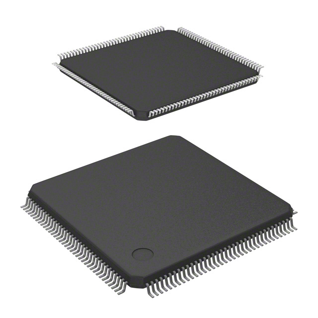
◼ Package:
LEP176
LES144
(S6J311xJAC*) * x: E/D
(S6J311xHzC*) * x: E/D, z: A/B
◼ CMOS 55 nm technology
◼ Power supply
5
V single power supply
voltage step-down circuit generates internal 1.2 V
from 5 V.
5 V power supply is used for I/O.
The
Page 2 of 120
�S6J311E, S6J311D
Table of Contents
1.
Product Lineup ............................................................................................................................................................ 4
2.
Pin Assignment ........................................................................................................................................................... 6
3.
Pin Description ............................................................................................................................................................ 8
4.
I/O Circuit Types ........................................................................................................................................................ 28
5.
Handling Precautions ............................................................................................................................................... 31
5.1
Precautions for Product Design ................................................................................................................................... 31
5.2
Precautions for Package Mounting .............................................................................................................................. 33
5.3
Precautions for Use Environment ................................................................................................................................ 35
6.
Handling Devices ...................................................................................................................................................... 36
7.
Block Diagram ........................................................................................................................................................... 39
8.
Memory Map ........................................................................................................................................................... 41
9.
Pin Statuses In CPU Status ...................................................................................................................................... 49
10.
Electrical Characteristics.......................................................................................................................................... 54
10.1 Absolute Maximum Ratings ......................................................................................................................................... 54
10.2 Recommended Operating Conditions.......................................................................................................................... 56
10.3 DC Characteristics....................................................................................................................................................... 59
10.4 AC Characteristics ....................................................................................................................................................... 63
10.4.1 Source Clock Timing .................................................................................................................................................... 63
10.4.2 Internal Clock Timing ................................................................................................................................................... 65
10.4.3 Reset Input ................................................................................................................................................................... 70
10.4.4 Power-on Conditions .................................................................................................................................................... 71
10.4.5 Multi-Function Serial .................................................................................................................................................... 72
10.5 Timer Input Timing....................................................................................................................................................... 96
10.6 Trigger Input Timing .................................................................................................................................................... 97
10.7 NMI Input Timing ......................................................................................................................................................... 98
10.8 Low-Voltage Detection (External Low-Voltage Detection) ........................................................................................... 99
10.9 Low-Voltage Detection (RAM Retention Low-Voltage Detection) .............................................................................. 100
10.10 Low-Voltage Detection (1.2 V Power Supply Low-Voltage Detection) ....................................................................... 100
10.11 A/D Converter ............................................................................................................................................................ 101
10.11.1 Electrical Characteristics...................................................................................................................................... 101
10.11.2 Notes on Using A/D Converter............................................................................................................................. 102
10.11.3 Definition of Terms ............................................................................................................................................... 103
10.12 Flash Memory ............................................................................................................................................................ 105
11.
Ordering Information .............................................................................................................................................. 106
12.
Part Number Option ................................................................................................................................................ 106
13.
Package Dimensions .............................................................................................................................................. 107
14.
Errata
......................................................................................................................................................... 109
15.
Appendix
......................................................................................................................................................... 113
15.1 Application 1: JTAG tool connection .......................................................................................................................... 113
16.
Major Changes......................................................................................................................................................... 114
Document History
......................................................................................................................................................... 119
Sales, Solutions, and Legal Information ........................................................................................................................... 120
Document Number: 002-05681 Rev. *G
Page 3 of 120
�S6J311E, S6J311D
1. Product Lineup
The following table lists the models available in the S6J3110 series.
Table 1-1 Memory Size
S6J311EyzC*
S6J311DyAC*
4096K bytes
Flash (Program)
3072K bytes
+
+
small sector (8KB x 8)
small sector (8KB x 8)
Flash (Work)
112K bytes
RAM (TCRAM)
64K bytes
RAM (System SRAM)
256K bytes
RAM (Backup RAM)
192K bytes
64K bytes
* y: J/H, z: A/B
Table 1-2 SHE Option
Security (SHE)
S6J311xyAC*
S6J311EHBC
ON
OFF
* x: E/D, y: J/H
Document Number: 002-05681 Rev. *G
Page 4 of 120
�S6J311E, S6J311D
Table 1-3 Comparison of models Available
S6J311xJAC*
* x:E/D
CPU core
CMOS 55 nm technology
Package
Main clock
Built-in CR oscillator
Maximum CPU operating frequency
Watchdog timer
Clock supervisor
External power supply, low-voltage detection reset
Internal power supply, low-voltage detection reset
NMI request
External interrupt
DMA controller
CAN-FD
Multi-function serial
A/D converter
Free-run timer
Input capture
Output compare
Base timer (16-bit)
Real time clock (RTC)
CR clock calibration
CRC generation
Low-power consumption mode
General-purpose port GPIO
Power supply
Operation assurance temperature (Ta)
On-chip debugger (JTAG)
Document Number: 002-05681 Rev. *G
S6J311xHzC*
* x:E/D, z: A/B
Coretex-R5
55 nm
LEP176
LES144
4 MHz
100 kHz
4 MHz
144 MHz (target)
1 channel (hardware)
1 channel (software)
Available
Available
Available
Available
16 channels
16 channels
2 channels
1 channel
(192 msg buffers/ch)
(192 msg buffers/ch)
22 channels
4 channels
12-bit (2 units)
12-bit (2 units)
Unit 0 x 32 channels
Unit 0 x 25 channels
Unit 1 x 32 channels
Unit 1 x 31 channels
6 channels
12 channels
12 channels
30 channels
1 channel
Available
Available
Standby function
Power-off function
Partial wakeup function
150 channels
116 channels
5 V + 5% to 10%
-40 °C to +105 °C
Available
Page 5 of 120
�S6J311E, S6J311D
2. Pin Assignment
The following figures show the pin assignment of the S6J3110 series.
176
175
174
173
172
171
170
169
168
167
166
165
164
163
162
161
160
159
158
157
156
155
154
153
152
151
150
149
148
147
146
145
144
143
142
141
140
139
138
137
136
135
134
133
VCC
P421/SIN2_1/SCS120_0/TRACECTL
P420/SCK2_1/SCK12_0/SCL12_0/TRACECLK
P419/SCS23_0/SOT12_0/SDA12_0/TIOA27_1
P418/SCS22_0/SIN12_0/INT14_0
P417/SOT7_1/SCS110_0/TIOA23_1/INT15_1
P416/IN5_0/SIN7_1/SCK11_0/SCL11_0/TIOA22_1
P415/SOT11_0/SDA11_0/TIOA26_1/INT13_0
P414/SCS21_0/SIN11_0
P413/SCS73_1/SCS20_0/INT14_1
P412/SCS72_1/TIOA25_1
P411/SCS71_1/SCK2_0/SCL2_0/INT13_1/TRACEDATA7
P410/SCS70_1
P409/SOT2_0/SDA2_0/TIOA24_1/TRACEDATA6
P408/SIN2_0/INT12_0/TRACEDATA5
P407/SCK7_1/SCK9_0/SCL9_0/TRACEDATA4
P406/SOT9_0/SDA9_0/TRACEDATA3
P405/IN4_0/SIN9_0/INT11_0/TRACEDATA2
P404/IN3_0/TRACEDATA1
P403/IN2_0/TRACEDATA0
P402/IN1_0/RX1_0/SCS63_1/SCS90_0/INT2_0
P401/IN0_0/TX1_0/SCS62_1
C
VSS
VCC
RSTX
P400/SCS61_1
P331/SCS60_1
VSS
X1
X0
MD
P330
P329/SIN6_1
P328/SOT6_1/SCS210_0
P327/SCK6_1/SCK21_0/SCL21_0
P326/SOT21_0/SDA21_0
P325/SIN21_0/INT10_0
TCK
TMS
TDI/P324
TDO/P323
TRST/P322
VCC
Figure 2-1 Pin Assignment for S6J311xJAC*
* x: E/D
VSS
P000/SOT2_1
P001/SCS20_1
P002/SCS21_1/TIOA0_1
P003/SCS22_1
P004/SCS23_1/TIOA1_1
P005/IN6_0/SIN3_0
P006/IN7_0/SOT3_0/SDA3_0
P007/IN8_0/SCK18_1/SCK3_0/SCL3_0
P008/IN9_0/SCS180_1/SCS30_0/TIOA0_0
P009/IN10_0/SIN8_0/TIOA1_0/INT0_1
P010/IN11_0/SOT8_0/SDA8_0/TIOA2_0
P011/SIN18_1/TIOA2_1
P012/OUT5_0/SCK8_0/SCL8_0/TIOA3_0
P013/OUT6_0/SCS80_0/TIOA4_0
P014/SOT18_1/TIOA3_1
P015/OUT7_0/SCS81_0/TIOA5_0
P016/OUT8_0/SCS82_0/TIOA6_0
P017/OUT9_0/SCS83_0/TIOA7_0
P018/OUT10_0/TIOA8_0
P019/OUT11_0/TIOB0_0/TEXT0_0
P020/SOT0_0/SDA0_0/TIOB1_0/TEXT1_0
P021/SCK4_1/SCK0_0/SCL0_0/TIOB2_0
P022/SIN0_0/TIOB3_0/INT3_0
P023/SIN4_1/SCS0_0/TIOB4_0
P024/SOT4_1/TIOB5_0
P025/SCS40_1
P026/SCS41_1
P027/SCS42_1/TIOA4_1/TIOB6_0/INT1_1/TEXT0_1
P028/OUT0_1/SIN1_0/TIOB7_0/INT4_0
P029/OUT1_1/SOT1_0/SDA1_0/AN0
P030/OUT2_1/SCS43_1
P031/OUT3_1/SCS1_0/AN1
P100/OUT4_1/SCK1_0/SCL1_0/AN2
P101/OUT5_1/AN3
P102/AN4
P103/OUT6_1/SIN17_0/AN5
P104/SOT17_0/SDA17_0
P105/OUT7_1/SCK17_0/SCL17_0/TIOA9_0
P106/OUT8_1/TX1_2/SCS170_0
P107/OUT9_1/RX1_2/SIN19_0/TIOA10_0/INT2_1
P108/OUT10_1/SOT19_0/SDA19_0/AN6/TIOA11_0/INT3_1
P109/OUT11_1/SIN19_1/SCK19_0/SCL19_0/TIOA12_0
VCC
1
2
3
4
5
6
7
8
9
10
11
12
13
14
15
16
17
18
19
20
21
22
23
24
25
26
27
28
29
30
31
32
33
34
35
36
37
38
39
40
41
42
43
44
●
TOP VIEW
LEP176
132
131
130
129
128
127
126
125
124
123
122
121
120
119
118
117
116
115
114
113
112
111
110
109
108
107
106
105
104
103
102
101
100
99
98
97
96
95
94
93
92
91
90
89
VSS
P321
P320/PWUTRG
P319/SIN7_0/AN63/INT12_1
P318/RX1_1/TIOA10_1/INT9_0
P317/TX1_1/AN62/TIOA9_1/INT11_1
P316/TIOA21_1
P315/IN5_1/SCS70_0/AN61/TIOA8_1
P314/IN4_1/SCK7_0/SCL7_0/AN60/TIOA7_1
P313/IN3_1/SOT7_0/SDA7_0/AN59/INT10_1
P312/IN2_1/SCS71_0/AN58
P311/SOT13_0/SDA13_0
P310/SIN13_0/INT15_0
P309/IN1_1/SCS130_0/AN57/TIOA29_1
P308/IN0_1/SCK13_0/SCL13_0/AN56/TIOA28_1
P307/RX0_0/SCS72_0/AN55/INT1_0
P306/TX0_0/SCS73_0/AN54
NMIX
P305/SCS140_0/AN53/TIOA29_0/TEXT5_0
P304/SCK14_0/SCL14_0/AN52/TIOA20_1/TEXT4_0
P303/SOT14_0/SDA14_0
P302/SIN14_0/AN51/TIOA19_1
P301/OUT4_0/SCS100_0/AN50/TIOA18_1
P300/OUT3_0/SCS101_0/AN49/TIOA28_0
P231/OUT2_0/SCS102_0/AN48/TIOA27_0
P230/OUT1_0/PWU_AN7/SCS103_0/AN47/TIOA26_0
P229/OUT0_0/PWU_AN6/RX0_1/SIN10_0/AN46/TIOA25_0/INT8_0
P228/PWU_AN5/TX0_1/SOT10_0/SDA10_0/AN45/TIOA24_0
P227/PWU_AN4/SCK10_0/SCL10_0/AN44/TIOA23_0
AVCC1
AVRH1
AVSS1/AVRL1
P226/IN11_2/PWU_AN3/SCK5_0/SCL5_0/AN43/TIOA17_1
P225/IN10_2/PWU_AN2/RX0_2/SOT5_0/SDA5_0/AN42/INT0_0
P224/IN9_2/PWU_AN1/TX0_2/SCS50_0/AN41
P223/IN8_2/PWU_AN0/SCS51_0/AN40
P222/IN7_2/SIN5_0/AN39/INT7_0
P221/SCS52_0
P220/IN6_2/SCS53_0/AN38
P219/SCS150_0/AN37/TEXT3_0
P218/SCK15_0/SCL15_0/AN36/TEXT2_0
P217/SOT15_0/SDA15_0
P216/SIN15_0
VSS
88
87
86
85
84
83
82
81
80
79
78
77
76
75
74
73
72
71
70
69
68
67
66
65
64
63
62
61
60
59
58
57
56
55
54
53
52
51
50
49
48
47
46
45
VCC
P215/IN5_2/SCK5_1/TIOA16_1/INT9_1
P214/IN4_2/SOT5_1/TIOA15_1
P213/IN3_2/SIN5_1/TIOA14_1/INT8_1
P212/IN2_2/SCS50_1/SCS41_0/AN35/TIOA13_1
P211/IN1_2/SCS40_0/AN34/TIOA22_0
P210/IN0_2/SIN4_0/AN33/TIOA21_0/INT6_0
P209/SOT4_0/SDA4_0/AN32/TIOA20_0
P208/SCS42_0/AN31/TIOA19_0
P207/SCK4_0/SCL4_0/AN30/INT7_1/TEXT5_1
P206/SCS43_0/AN29/TEXT4_1
P205/SCK20_0/SCL20_0/AN28/TEXT3_1
P204/IN11_1/SOT20_0/SDA20_0/AN27
P203/IN10_1
P202/IN9_1/SCK6_0/SCL6_0/INT6_1
P201/SIN20_0/AN26/TIOA18_0
P200/SCS202_0/AN25/TIOA17_0
P131/IN8_1/SOT6_0/SDA6_0/AN24
P130/IN7_1/SIN6_0/AN23/INT5_0
P129/IN6_1/SCS201_0/AN22
P128/SCS200_0/AN21/TEXT2_1
P127/SCS203_0/AN20/TEXT1_1
P126/SCK16_0/SCL16_0/AN19
P125/SOT16_0/SDA16_0/TIOA16_0
P124/SIN16_0/TIOA15_0
P123/SCS63_0/AN18/TIOA12_1
P122/SCS62_0/AN17/TIOA11_1
P121/SCS160_0/AN16/TIOA14_0
P120/SCS61_0/AN15
P119/SCS60_0/AN14
P118/AN13/INT5_1
P117/AN12/INT4_1
P116/AN11
P115
AVSS0/AVRL0
AVRH0
AVCC0
P114/SCS180_0/AN10/TIOA6_1
P113/SOT19_1/SCK18_0/SCL18_0/TIOA5_1
P112/SOT18_0/SDA18_0/AN9/TIOA13_0
P111/SIN18_0/AN8
P110/SCS190_0/AN7
C
VSS
Document Number: 002-05681 Rev. *G
Page 6 of 120
�S6J311E, S6J311D
Figure 2-2 Pin Assignment for S6J311xHzC*
144
143
142
141
140
139
138
137
136
135
134
133
132
131
130
129
128
127
126
125
124
123
122
121
120
119
118
117
116
115
114
113
112
111
110
109
VCC
P421/SIN2_1/TRACECTL
P420/SCK2_1/TRACECLK
P418/SCS22_0/INT14_0
P417/TIOA23_1/INT15_1
P416/IN5_0/TIOA22_1
P414/SCS21_0
P413/SCS20_0/INT14_1
P411/INT13_1/SCK2_0/SCL2_0/TRACEDATA7
P409/SOT2_0/SDA2_0/TIOA24_1/TRACEDATA6
P408/SIN2_0/INT12_0/TRACEDATA5
P407/TRACEDATA4
P406/TRACEDATA3
P405/IN4_0/INT11_0/TRACEDATA2
P404/IN3_0/TRACEDATA1
P403/IN2_0/TRACEDATA0
P402/IN1_0/INT2_0
P401/IN0_0
C
VSS
VCC
RSTX
P400
P331
VSS
X1
X0
MD
P330
P327
TCK
TMS
TDI/P324
TDO/P323
TRST/P322
VCC
* x: E/D, z: A/B
VSS
P000/SOT2_1
P001/SCS20_1
P003/SCS22_1
P005/IN6_0/SIN3_0
P006/SOT3_0/SDA3_0/IN7_0
P007/SCK3_0/SCL3_0/IN8_0
P008/IN9_0/SCS30_0/TIOA0_0
P009/IN10_0/TIOA1_0/INT0_1
P010/IN11_0/TIOA2_0
P012/OUT5_0/TIOA3_0
P013/OUT6_0/TIOA4_0
P015/OUT7_0/TIOA5_0
P016/OUT8_0/TIOA6_0
P017/OUT9_0/TIOA7_0
P018/OUT10_0/TIOA8_0
P019/OUT11_0/TIOB0_0/TEXT0_0
P020/SOT0_0/SDA0_0/TEXT1_0/TIOB1_0
P021/SCK0_0/SCL0_0/TIOB2_0
P022/SIN0_0/TIOB3_0/INT3_0
P023/SCS0_0/TIOB4_0
P024/TIOB5_0
P027/TIOA4_1/TIOB6_0/INT1_1/TEXT0_1
P028/OUT0_1/SIN1_0/TIOB7_0/INT4_0
P029/AN0/SOT1_0/SDA1_0/OUT1_1
P030/OUT2_1
P031/OUT3_1/SCS1_0/AN1
P100/AN2/SCK1_0/SCL1_0/OUT4_1
P101/OUT5_1/AN3
P103/OUT6_1/AN5
P105/OUT7_1/TIOA9_0
P106/OUT8_1
P107/OUT9_1/TIOA10_0/INT2_1
P108/OUT10_1/AN6/TIOA11_0/INT3_1
P109/OUT11_1/TIOA12_0
VCC
1
2
3
4
5
6
7
8
9
10
11
12
13
14
15
16
17
18
19
20
21
22
23
24
25
26
27
28
29
30
31
32
33
34
35
36
●
TOP VIEW
LES144
108
107
106
105
104
103
102
101
100
99
98
97
96
95
94
93
92
91
90
89
88
87
86
85
84
83
82
81
80
79
78
77
76
75
74
73
VSS
P321/PWUTRG
NC
NC
P317/AN62/TIOA9_1/INT11_1
P315/IN5_1/AN61/TIOA8_1
P314/IN4_1/AN60/TIOA7_1
P313/IN3_1/AN59/INT10_1
P312/IN2_1/AN58
P309/IN1_1/AN57/TIOA29_1
P308/IN0_1/AN56/TIOA28_1
P307/RX0_0/AN55/INT1_0
P306/TX0_0/AN54
NMIX
P305/AN53/TIOA29_0/TEXT5_0
P304/AN52/TIOA20_1/TEXT4_0
P302/AN51/TIOA19_1
P301/OUT4_0/AN50/TIOA18_1
P300/OUT3_0/AN49/TIOA28_0
P231/OUT2_0/AN48/TIOA27_0
P230/OUT1_0/PWU_AN7/AN47/TIOA26_0
P229/OUT0_0/PWU_AN6/RX0_1/AN46/TIOA25_0/INT8_0
P228/PWU_AN5/TX0_1/AN45/TIOA24_0
P227/PWU_AN4/AN44/TIOA23_0
AVCC1
AVRH1
AVSS1/AVRL1
P226/IN11_2/PWU_AN3/AN43/TIOA17_1
P225/IN10_2/PWU_AN2/RX0_2/AN42/INT0_0
P224/IN9_2/PWU_AN1/TX0_2/AN41
P223/IN8_2/PWU_AN0/AN40
P222/IN7_2/AN39/INT7_0
P220/IN6_2/AN38
P219/AN37/TEXT3_0
P218/AN36/TEXT2_0
VSS
72
71
70
69
68
67
66
65
64
63
62
61
60
59
58
57
56
55
54
53
52
51
50
49
48
47
46
45
44
43
42
41
40
39
38
37
VCC
P215/IN5_2/TIOA16_1/INT9_1
P214/IN4_2/TIOA15_1
P213/IN3_2/TIOA14_1/INT8_1
P212/IN2_2/AN35/TIOA13_1
P211/IN1_2/AN34/TIOA22_0
P210/IN0_2/AN33/TIOA21_0/INT6_0
P209/AN32/TIOA20_0
P208/AN31/TIOA19_0
P207/AN30/INT7_1/TEXT5_1
P206/AN29/TEXT4_1
P205/AN28/TEXT3_1
P204/IN11_1/AN27
P203/IN10_1
P202/IN9_1/INT6_1
P131/IN8_1/AN24
P130/IN7_1/AN23/INT5_0
P129/IN6_1/AN22
P128/AN21/TEXT2_1
P127/AN20/TEXT1_1
P126/AN19
P123/AN18/TIOA12_1
P122/AN17/TIOA11_1
P120/AN15
P119/AN14
P118/AN13/INT5_1
P117/AN12/INT4_1
P115
AVSS0/AVRL0
AVRH0
AVCC0
P114/AN10/TIOA6_1
P113/TIOA5_1
P112/AN9/TIOA13_0
C
VSS
Document Number: 002-05681 Rev. *G
Page 7 of 120
�S6J311E, S6J311D
3. Pin Description
This section provides a list of the pin functions of the S6J3110 series
Table 3-1 S6J311xJAC* Pin Functions
* x: E/D
Pin No.
S6J311xJAC
Pin Name
Polarity I/O Circuit Type
Function
2
P000
SOT2_1
-
P
General-purpose I/O port
Multi-function serial ch.2 serial data output pin (1)
3
P001
SCS20_1
-
P
General-purpose I/O port
Multi-function serial ch.2 chip select 0 I/O pin (1)
4
P002
SCS21_1
TIOA0_1
-
P
General-purpose I/O port
Multi-function serial ch.2 chip select 1 output pin (1)
Base timer ch.0 TIOA output pin (1)
5
P003
SCS22_1
-
P
General-purpose I/O port
Multi-function serial ch.2 chip select 2 output pin (1)
P004
SCS23_1
TIOA1_1
P005
IN6_0
SIN3_0
P006
IN7_0
SOT3_0
SDA3_0
P007
IN8_0
SCK18_1
SCK3_0
SCL3_0
P008
IN9_0
SCS180_1
SCS30_0
TIOA0_0
P009
IN10_0
SIN8_0
TIOA1_0
INT0_1
P010
IN11_0
SOT8_0
SDA8_0
TIOA2_0
P011
SIN18_1
TIOA2_1
P012
SCK8_0
SCL8_0
TIOA3_0
OUT5_0
-
6
7
8
9
10
11
12
13
14
Document Number: 002-05681 Rev. *G
P
P
P
P
P
P
P
P
P
General-purpose I/O port
Multi-function serial ch.3 chip select 2 output pin (1)
Base timer ch.1 TIOA output pin (1)
General-purpose I/O port
Input capture ch.6 input pin (0)
Multi-function serial ch.3 serial data input pin (0)
General-purpose I/O port
Input capture ch.7 input pin (0)
Multi-function serial ch.3 serial data output pin (0)
I2C bus ch.3 serial data I/O pin
General-purpose I/O port
Input capture ch.8 input pin (0)
Multi-function serial ch.18 clock I/O pin (1)
Multi-function serial ch.3 clock I/O pin (0)
I2C bus ch.3 serial clock I/O pin
General-purpose I/O port
Input capture ch.9 input pin (0)
Multi-function serial ch.18 chip select 0 I/O pin (1)
Multi-function serial ch.3 chip select 0 I/O pin (0)
Base timer ch.0 TIOA output pin (0)
General-purpose I/O port
Input capture ch.10 input pin (0)
Multi-function serial ch.8 serial data input pin (0)
Base timer ch.1 TIOA I/O pin (0)
INT0 external interrupt input pin (1)
General-purpose I/O port
Input capture ch.11 input pin (0)
Multi-function serial ch.8 serial data output pin (0)
I2C bus ch.8 serial data I/O pin
Base timer ch.2 TIOA output pin (0)
General-purpose I/O port
Multi-function serial ch.18 serial data input pin (1)
Base timer ch.2 TIOA output pin (1)
General-purpose I/O port
Multi-function serial ch.8 clock I/O pin (0)
I2C bus ch.8 serial clock I/O pin
Base timer ch.3 TIOA I/O pin (0)
Output compare ch.5 output pin (0)
Page 8 of 120
�S6J311E, S6J311D
Pin No.
S6J311xJAC
15
16
17
18
19
20
21
22
23
24
25
26
27
28
29
Pin Name
P013
SCS80_0
TIOA4_0
OUT6_0
P014
SOT18_1
TIOA3_1
P015
SCS81_0
TIOA5_0
OUT7_0
P016
SCS82_0
TIOA6_0
OUT8_0
P017
SCS83_0
TIOA7_0
OUT9_0
P018
TIOA8_0
OUT10_0
P019
OUT11_0
TIOB0_0
TEXT0_0
P020
SOT0_0
SDA0_0
TIOB1_0
TEXT1_0
P021
SCK4_1
TIOB2_0
SCK0_0
SCL0_0
P022
SIN0_0
TIOB3_0
INT3_0
P023
SIN4_1
SCS0_0
TIOB4_0
P024
SOT4_1
TIOB5_0
P025
SCS40_1
P026
SCS41_1
P027
SCS42_1
TIOA4_1
TIOB6_0
INT1_1
TEXT0_1
Document Number: 002-05681 Rev. *G
Polarity I/O Circuit Type
-
P
P
P
P
P
P
P
P
P
P
P
P
P
P
P
Function
General-purpose I/O port
Multi-function serial ch.8 chip select 0 I/O pin (0)
Base timer ch.4 TIOA output pin (0)
Output compare ch.6 output pin (0)
General-purpose I/O port
Multi-function serial ch.18 serial data output pin (1)
Base timer ch.3 TIOA output pin (1)
General-purpose I/O port
Multi-function serial ch.8 chip select 1 output pin (0)
Base timer ch.5 TIOA I/O pin (0)
Output compare ch.7 output pin (0)
General-purpose I/O port
Multi-function serial ch.8 chip select 2 output pin (0)
Base timer ch.6 TIOA output pin (0)
Output compare ch.8 output pin (0)
General-purpose I/O port
Multi-function serial ch.8 chip select 3 output pin (0)
Base timer ch.7 TIOA I/O pin (0)
Output compare ch.9 output pin (0)
General-purpose I/O port
Base timer ch.8 TIOA output pin (0)
Output compare ch.10 output pin (0)
General-purpose I/O port
Output compare ch.11 output pin (0)
Base timer ch.0 TIOB input pin (0)
Free-run timer 0 clock input pin (0)
General-purpose I/O port
Multi-function serial ch.0 serial data output pin (0)
I2C bus ch.0 serial data I/O pin
Base timer ch.1 TIOB input pin (0)
Free-run timer 1 clock input pin (0)
General-purpose I/O port
Multi-function serial ch.4 clock I/O pin (1)
Base timer ch.2 TIOB input pin (0)
Multi-function serial ch.0 clock I/O pin (0)
I2C bus ch.0 serial clock I/O pin
General-purpose I/O port
Multi-function serial ch.0 serial data input pin (0)
Base timer ch.3 TIOB input pin (0)
INT3 external interrupt input pin (0)
General-purpose I/O port
Multi-function serial ch.4 serial data input pin (1)
Multi-function serial ch.0 chip select I/O pin (0)
Base timer ch.4 TIOB input pin (0)
General-purpose I/O port
Multi-function serial ch.4 serial data output pin (1)
Base timer ch.5 TIOB input pin (0)
General-purpose I/O port
Multi-function serial ch.4 chip select 0 I/O pin (1)
General-purpose I/O port
Multi-function serial ch.4 chip select 1 output pin (1)
General-purpose I/O port
Multi-function serial ch.4 chip select 2 output pin (1)
Base timer ch.4 TIOA output pin (1)
Base timer ch.6 TIOB input pin (0)
INT1 external interrupt input pin (1)
Free-run timer 0 clock input pin (1)
Page 9 of 120
�S6J311E, S6J311D
Pin No.
S6J311xJAC
30
31
32
33
34
35
36
37
38
39
40
41
42
Pin Name
P028
SIN1_0
TIOB7_0
INT4_0
OUT0_1
P029
SOT1_0
SDA1_0
AN0
OUT1_1
P030
SCS43_1
OUT2_1
P031
SCS1_0
AN1
OUT3_1
P100
SCK1_0
SCL1_0
AN2
OUT4_1
P101
AN3
OUT5_1
P102
AN4
P103
SIN17_0
AN5
OUT6_1
P104
SOT17_0
SDA17_0
P105
SCK17_0
SCL17_0
TIOA9_0
OUT7_1
P106
TX1_2
SCS170_0
OUT8_1
P107
RX1_2
SIN19_0
TIOA10_0
INT2_1
OUT9_1
P108
SOT19_0
SDA19_0
AN6
TIOA11_0
INT3_1
OUT10_1
Document Number: 002-05681 Rev. *G
Polarity I/O Circuit Type
-
P
A
P
A
A
A
A
A
P
P
P
P
A
Function
General-purpose I/O port
Multi-function serial ch.1 serial data input pin (0)
Base timer ch.7 TIOB input pin (0)
INT4 external interrupt input pin (0)
Output compare ch.0 output pin (1)
General-purpose I/O port
Multi-function serial ch.1 serial data output pin (0)
I2C bus ch.1 serial data I/O pin
ADC analog 0 input pin
Output compare ch.1 output pin (1)
General-purpose I/O port
Multi-function serial chip ch.4 select 3 output pin (1)
Output compare ch.2 output pin (1)
General-purpose I/O port
Multi-function serial ch.1 chip select I/O pin (0)
ADC analog 1 input pin
Output compare ch.3 output pin (1)
General-purpose I/O port
Multi-function serial ch.1 clock I/O pin (0)
I2C bus ch.1 serial clock I/O pin
ADC analog 2 input pin
Output compare ch.4 output pin (1)
General-purpose I/O port
ADC analog 3 input pin
Output compare ch.5 output pin (1)
General-purpose I/O port
ADC analog 4 input pin
General-purpose I/O port
Multi-function serial ch.17 serial data input pin (0)
ADC analog 5 input pin
Output compare ch.6 output pin (1)
General-purpose I/O port
Multi-function serial ch.17 serial data output pin (0)
I2C bus ch.17 serial data I/O pin
General-purpose I/O port
Multi-function serial ch.17 clock I/O pin (0)
I2C bus ch.17 serial clock I/O pin
Base timer ch.9 TIOA output pin (0)
Output compare ch.7 output pin (1)
General-purpose I/O port
CAN transmission data 1 output pin (2)
Multi-function serial ch.17 chip select 0 I/O pin (0)
Output compare ch.8 output pin (1)
General-purpose I/O port
CAN reception data 1 input pin (2)
Multi-function serial ch.19 serial data input pin (0)
Base timer ch.10 TIOA output pin (0)
INT2 external interrupt input pin (1)
Output compare ch.9 output pin (1)
General-purpose I/O port
Multi-function serial ch.19 serial data output pin (0)
I2C bus ch.19 serial data I/O pin
ADC analog 6 input pin
Base timer ch.11 TIOA output pin (0)
INT3 external interrupt input pin (1)
Output compare ch.10 output pin (1)
Page 10 of 120
�S6J311E, S6J311D
Pin No.
S6J311xJAC
43
47
48
49
50
51
55
56
57
58
59
60
61
62
63
64
Pin Name
Polarity I/O Circuit Type
P109
SIN19_1
SCK19_0
SCL19_0
TIOA12_0
OUT11_1
P110
SCS190_0
AN7
P111
SIN18_0
AN8
P112
SOT18_0
SDA18_0
AN9
TIOA13_0
P113
SOT19_1
SCK18_0
SCL18_0
TIOA5_1
P114
SCS180_0
AN10
TIOA6_1
-
P115
-
P116
AN11
P117
AN12
INT4_1
P118
AN13
INT5_1
P119
SCS60_0
AN14
P120
SCS61_0
AN15
P121
SCS160_0
AN16
TIOA14_0
P122
SCS62_0
AN17
TIOA11_1
P123
SCS63_0
AN18
TIOA12_1
P124
SIN16_0
TIOA15_0
-
Document Number: 002-05681 Rev. *G
P
A
A
A
P
A
P
A
A
A
A
A
A
A
A
P
Function
General-purpose I/O port
Multi-function serial ch.19 serial data input pin (1)
Multi-function serial ch.19 clock I/O pin (0)
I2C bus ch.19 serial clock I/O pin
Base timer ch.12 TIOA output pin (0)
Output compare ch.11 output pin (1)
General-purpose I/O port
Multi-function serial ch.19 chip select 0 I/O pin (0)
ADC analog 7 input pin
General-purpose I/O port
Multi-function serial ch.18 serial data input pin (0)
ADC analog 8 input pin
General-purpose I/O port
Multi-function serial ch.18 serial data output pin (0)
I2C bus ch.18 serial data I/O pin
ADC analog 9 input pin
Base timer ch.13 TIOA output pin (0)
General-purpose I/O port
Multi-function serial ch.19 serial data output pin (1)
Multi-function serial ch.18 clock I/O pin (0)
I2C bus ch.18 serial clock I/O pin
Base timer ch.5 TIOA output pin (1)
General-purpose I/O port
Multi-function serial ch.18 chip select 0 I/O pin (0)
ADC analog 10 input pin
Base timer ch.6 TIOA output pin (1)
General-purpose I/O port
General-purpose I/O port
ADC analog 11 input pin
General-purpose I/O port
ADC analog 12 input pin
INT4 external interrupt input pin (1)
General-purpose I/O port
ADC analog 13 input pin
INT5 external interrupt input pin (1)
General-purpose I/O port
Multi-function serial ch.6 chip select 0 I/O pin (0)
ADC analog 14 input pin
General-purpose I/O port
Multi-function serial ch.6 chip select 1 output pin (0)
ADC analog 15 input pin
General-purpose I/O port
Multi-function serial ch.16 chip select 0 I/O pin (0)
ADC analog 16 input pin
Base timer ch.14 TIOA output pin (0)
General-purpose I/O port
Multi-function serial ch.6 chip select 2 output pin (0)
ADC analog 17 input pin
Base timer ch.11 TIOA output pin (1)
General-purpose I/O port
Multi-function serial ch.6 chip select 3 output pin (0)
ADC analog 18 input pin
Base timer ch.12 TIOA output pin (1)
General-purpose I/O port
Multi-function serial ch.16 serial data input pin (0)
Base timer ch.15 TIOA output pin (0)
Page 11 of 120
�S6J311E, S6J311D
Pin No.
S6J311xJAC
65
66
67
68
69
70
71
72
73
74
75
76
77
78
Pin Name
P125
SOT16_0
SDA16_0
TIOA16_0
P126
SCK16_0
SCL16_0
AN19
P127
SCS203_0
AN20
TEXT1_1
P128
SCS200_0
AN21
TEXT2_1
P129
IN6_1
SCS201_0
AN22
P130
IN7_1
SIN6_0
AN23
INT5_0
P131
IN8_1
SOT6_0
SDA6_0
AN24
P200
SCS202_0
AN25
TIOA17_0
P201
SIN20_0
AN26
TIOA18_0
P202
IN9_1
SCK6_0
SCL6_0
INT6_1
P203
IN10_1
P204
IN11_1
SOT20_0
SDA20_0
AN27
P205
SCK20_0
SCL20_0
AN28
TEXT3_1
P206
SCS43_0
AN29
TEXT4_1
Document Number: 002-05681 Rev. *G
Polarity I/O Circuit Type
-
P
A
A
A
A
A
A
A
A
P
P
A
A
A
Function
General-purpose I/O port
Multi-function serial ch.16 serial data output pin (0)
I2C bus ch.16 serial data I/O pin
Base timer ch.16 TIOA output pin (0)
General-purpose I/O port
Multi-function serial ch.16 clock I/O pin (0)
I2C bus ch.16 serial clock I/O pin
ADC analog 19 input pin
General-purpose I/O port
Multi-function serial ch.20 chip select 3 output pin (0)
ADC analog 20 input pin
Free-run timer 1 clock input pin (1)
General-purpose I/O port
Multi-function serial ch.20 chip select 0 I/O pin (0)
ADC analog 21 input pin
Free-run timer 2 clock input pin (1)
General-purpose I/O port
Input capture ch.6 input pin (1)
Multi-function serial ch.20 chip select 1 output pin (0)
ADC analog 22 input pin
General-purpose I/O port
Input capture ch.7 input pin (1)
Multi-function serial ch.6 serial data input pin (0)
ADC analog 23 input pin
INT5 external interrupt input pin (0)
General-purpose I/O port
Input capture ch.8 input pin (1)
Multi-function serial ch.6 serial data output pin (0)
I2C bus ch.6 serial data I/O pin
ADC analog 24 input pin
General-purpose I/O port
Multi-function serial ch.20 chip select 2 output pin (0)
ADC analog 25 input pin
Base timer ch.17 TIOA output pin (0)
General-purpose I/O port
Multi-function serial ch.20 serial data input pin (0)
ADC analog 26 input pin
Base timer ch.18 TIOA output pin (0)
General-purpose I/O port
Input capture ch.9 input pin (1)
Multi-function serial ch.6 clock I/O pin (0)
I2C bus ch.6 serial clock I/O pin
INT6 external interrupt input pin (1)
General-purpose I/O port
Input capture ch.10 input pin (1)
General-purpose I/O port
Input capture ch.11 input pin (1)
Multi-function serial ch.20 serial data output pin (0)
I2C bus ch.20 serial data I/O pin
ADC analog 27 input pin
General-purpose I/O port
Multi-function serial ch.20 clock I/O pin (0)
I2C bus ch.20 serial clock I/O pin
ADC analog 28 input pin
Free-run timer 3 clock input pin (1)
General-purpose I/O port
Multi-function serial ch.4 chip select 3 output pin (0)
ADC analog 29 input pin
Free-run timer 4 clock input pin (1)
Page 12 of 120
�S6J311E, S6J311D
Pin No.
S6J311xJAC
79
80
81
82
83
84
85
86
87
90
91
92
Pin Name
P207
SCK4_0
SCL4_0
AN30
INT7_1
TEXT5_1
P208
SCS42_0
AN31
TIOA19_0
P209
SOT4_0
SDA4_0
AN32
TIOA20_0
P210
IN0_2
SIN4_0
AN33
TIOA21_0
INT6_0
P211
IN1_2
SCS40_0
AN34
TIOA22_0
P212
IN2_2
SCS50_1
SCS41_0
AN35
TIOA13_1
P213
IN3_2
SIN5_1
TIOA14_1
INT8_1
P214
IN4_2
SOT5_1
TIOA15_1
P215
IN5_2
SCK5_1
TIOA16_1
INT9_1
P216
SIN15_0
P217
SOT15_0
SDA15_0
P218
SCK15_0
SCL15_0
AN36
TEXT2_0
Document Number: 002-05681 Rev. *G
Polarity I/O Circuit Type
-
A
A
A
A
A
A
P
P
P
P
P
A
Function
General-purpose I/O port
Multi-function serial ch.4 clock I/O pin (0)
I2C bus ch.4 serial clock I/O pin
ADC analog 30 input pin
INT7 external interrupt input pin (1)
Free-run timer 5 clock input pin (1)
General-purpose I/O port
Multi-function serial ch.4 chip select 2 output pin (0)
ADC analog 31 input pin
Base timer ch.19 TIOA output pin (0)
General-purpose I/O port
Multi-function serial ch.4 serial data output pin (0)
I2C bus ch.4 serial data I/O pin
ADC analog 32 input pin
Base timer ch.20 TIOA output pin (0)
General-purpose I/O port
Input capture ch.0 input pin (2)
Multi-function serial ch.4 serial data input pin (0)
ADC analog 33 input pin
Base timer ch.21 TIOA output pin (0)
INT6 external interrupt input pin (0)
General-purpose I/O port
Input capture ch.1 input pin (2)
Multi-function serial ch.4 chip select 0 I/O pin (0)
ADC analog 34 input pin
Base timer ch.22 TIOA output pin (0)
General-purpose I/O port
Input capture ch.2 input pin (2)
Multi-function serial ch.5 chip select 0 I/O pin (1)
Multi-function serial ch.4 chip select 1 output pin (0)
ADC analog 35 input pin
Base timer ch.13 TIOA output pin (1)
General-purpose I/O port
Input capture ch.3 input pin (2)
Multi-function serial ch.5 serial data input pin (1)
Base timer ch.14 TIOA output pin (1)
INT8 external interrupt input pin (1)
General-purpose I/O port
Input capture ch.4 input pin (2)
Multi-function serial ch.5 serial data output pin (1)
Base timer ch.15 TIOA output pin (1)
General-purpose I/O port
Input capture ch.5 input pin (2)
Multi-function serial ch.5 clock I/O pin (1)
Base timer ch.16 TIOA output pin (1)
INT9 external interrupt input pin (1)
General-purpose I/O port
Multi-function serial ch.15 serial data input pin (0)
General-purpose I/O port
Multi-function serial ch.15 serial data output pin (0)
I2C bus ch.15 serial data I/O pin
General-purpose I/O port
Multi-function serial ch.15 clock I/O pin (0)
I2C bus ch.15 serial clock I/O pin
ADC analog 36 input pin
Free-run timer 2 clock input pin (0)
Page 13 of 120
�S6J311E, S6J311D
Pin No.
S6J311xJAC
93
94
95
96
97
98
99
100
104
105
Pin Name
P219
SCS150_0
AN37
TEXT3_0
P220
IN6_2
SCS53_0
AN38
P221
SCS52_0
P222
IN7_2
SIN5_0
AN39
INT7_0
P223
IN8_2
PWU_AN0
SCS51_0
AN40
P224
IN9_2
PWU_AN1
TX0_2
SCS50_0
AN41
P225
IN10_2
PWU_AN2
RX0_2
SOT5_0
SDA5_0
AN42
INT0_0
P226
IN11_2
PWU_AN3
SCK5_0
SCL5_0
AN43
TIOA17_1
P227
PWU_AN4
SCK10_0
SCL10_0
AN44
TIOA23_0
P228
PWU_AN5
TX0_1
SOT10_0
SDA10_0
AN45
TIOA24_0
Document Number: 002-05681 Rev. *G
Polarity I/O Circuit Type
-
A
A
P
A
A
A
A
A
A
A
Function
General-purpose I/O port
Multi-function serial ch.15 chip select 0 I/O pin (0)
ADC analog 37 input pin
Free-run timer 3 clock input pin (0)
General-purpose I/O port
Input capture ch.6 input pin (2)
Multi-function serial ch.5 chip select 3 output pin (0)
ADC analog 38 input pin
General-purpose I/O port
Multi-function serial ch.5 chip select 2 output pin (0)
General-purpose I/O port
Input capture ch.7 input pin (2)
Multi-function serial ch.5 serial data input pin (0)
ADC analog 39 input pin
INT7 external interrupt input pin (0)
General-purpose I/O port
Input capture ch.8 input pin (2)
Partial wakeup ADC analog 0 input pin
Multi-function serial ch.5 chip select 1 output pin (0)
ADC analog 40 input pin
General-purpose I/O port
Input capture ch.9 input pin (2)
Partial wakeup ADC analog 1 input pin
CAN transmission data 0 output pin (2)
Multi-function serial ch.5 chip select 0 I/O pin (0)
ADC analog 41 input pin
General-purpose I/O port
Input capture ch.10 input pin (2)
Partial wakeup ADC analog 2 input pin
CAN reception data 0 input pin (2)
Multi-function serial ch.5 serial data output pin (0)
I2C bus ch.5 serial data I/O pin
ADC analog 42 input pin
INT0 external interrupt input pin (0)
General-purpose I/O port
Input capture ch.11 input pin (2)
Partial wakeup ADC analog 3 input pin
Multi-function serial ch.5 clock I/O pin (0)
I2C bus ch.5 serial clock I/O pin
ADC analog 43 input pin
Base timer ch.17 TIOA output pin (1)
General-purpose I/O port
Partial wakeup ADC analog 4 input pin
Multi-function serial ch.10 clock I/O pin (0)
I2C bus ch.10 serial clock I/O pin
ADC analog 44 input pin
Base timer ch.23 TIOA output pin (0)
General-purpose I/O port
Partial wakeup ADC analog 5 input pin
CAN transmission data 0 output pin (1)
Multi-function serial ch.10 serial data output pin (0)
I2C bus ch.10 serial data I/O pin
ADC analog 45 input pin
Base timer ch.24 TIOA output pin (0)
Page 14 of 120
�S6J311E, S6J311D
Pin No.
S6J311xJAC
106
107
108
109
110
111
112
113
114
115
116
117
Pin Name
Polarity I/O Circuit Type
P229
PWU_AN6
RX0_1
SIN10_0
AN46
TIOA25_0
INT8_0
OUT0_0
P230
PWU_AN7
SCS103_0
AN47
TIOA26_0
OUT1_0
P231
SCS102_0
AN48
TIOA27_0
OUT2_0
P300
SCS101_0
AN49
TIOA28_0
OUT3_0
P301
SCS100_0
AN50
TIOA18_1
OUT4_0
P302
SIN14_0
AN51
TIOA19_1
P303
SOT14_0
SDA14_0
P304
SCK14_0
SCL14_0
AN52
TIOA20_1
TEXT4_0
P305
SCS140_0
AN53
TIOA29_0
TEXT5_0
-
NMIX
N
P306
TX0_0
SCS73_0
AN54
P307
RX0_0
SCS72_0
AN55
INT1_0
-
Document Number: 002-05681 Rev. *G
A
A
A
A
A
A
P
A
A
F
A
A
Function
General-purpose I/O port
Partial wakeup ADC analog 6 input pin
CAN reception data 0 input pin (1)
Multi-function serial ch.10 serial data input pin (0)
ADC analog 46 input pin
Base timer ch.25 TIOA output pin (0)
INT8 external interrupt input pin (0)
Output compare ch.0 output pin (0)
General-purpose I/O port
Partial wakeup ADC analog 7 input pin
Multi-function serial ch.10 chip select 3 output pin (0)
ADC analog 47 input pin
Base timer ch.26 TIOA output pin (0)
Output compare ch.1 output pin (0)
General-purpose I/O port
Multi-function serial ch.10 chip select 2 output pin (0)
ADC analog 48 input pin
Base timer ch.27 TIOA output pin (0)
Output compare ch.2 output pin (0)
General-purpose I/O port
Multi-function serial ch.10 chip select 1 output pin (0)
ADC analog 49 input pin
Base timer ch.28 TIOA output pin (0)
Output compare ch.3 output pin (0)
General-purpose I/O port
Multi-function serial ch.10 chip select 0 I/O pin (0)
ADC analog 50 input pin
Base timer ch.18 TIOA output pin (1)
Output compare ch.4 output pin (0)
General-purpose I/O port
Multi-function serial ch.14 serial data input pin (0)
ADC analog 51 input pin
Base timer ch.19 TIOA output pin (1)
General-purpose I/O port
Multi-function serial ch.14 serial data output pin (0)
I2C bus ch.14 serial data I/O pin
General-purpose I/O port
Multi-function serial ch.14 clock I/O pin (0)
I2C bus ch.14 serial clock I/O pin
ADC analog 52 input pin
Base timer ch.20 TIOA output pin (1)
Free-run timer 4 clock input pin (0)
General-purpose I/O port
Multi-function serial ch.14 chip select 0 I/O pin (0)
ADC analog 53 input pin
Base timer ch.29 TIOA output pin (0)
Free-run timer 5 clock input pin (0)
Non-maskable interrupt input pin
General-purpose I/O port
CAN transmission data 0 output pin (0)
Multi-function serial ch.7 chip select 3 output pin (0)
ADC analog 54 input pin
General-purpose I/O port
CAN reception data 0 input pin (0)
Multi-function serial ch.7 chip select 2 output pin (0)
ADC analog 55 input pin
INT1 external interrupt input pin (0)
Page 15 of 120
�S6J311E, S6J311D
Pin No.
S6J311xJAC
Pin Name
Polarity I/O Circuit Type
Function
-
131
P308
IN0_1
SCK13_0
SCL13_0
AN56
TIOA28_1
P309
IN1_1
SCS130_0
AN57
TIOA29_1
P310
SIN13_0
INT15_0
P311
SOT13_0
SDA13_0
P312
IN2_1
SCS71_0
AN58
P313
IN3_1
SOT7_0
SDA7_0
AN59
INT10_1
P314
IN4_1
SCK7_0
SCL7_0
AN60
TIOA7_1
P315
IN5_1
SCS70_0
AN61
TIOA8_1
P316
TIOA21_1
P317
TX1_1
AN62
TIOA9_1
INT11_1
P318
RX1_1
TIOA10_1
INT9_0
P319
SIN7_0
AN63
INT12_1
P320
PWUTRG
P321
-
D
General-purpose output port
134
TRST
P322
N
-
J
JTAG test reset input pin
General-purpose output port
118
119
120
121
122
123
124
125
126
127
128
129
130
Document Number: 002-05681 Rev. *G
A
A
P
P
A
A
A
A
P
A
P
A
P
General-purpose I/O port
Input capture ch.0 input pin (1)
Multi-function serial ch.13 clock I/O pin (0)
I2C bus ch.13 serial clock I/O pin
ADC analog 56 input pin
Base timer ch.28 TIOA output pin (1)
General-purpose I/O port
Input capture ch.1 input pin (1)
Multi-function serial ch.13 chip select 0 I/O pin (0)
ADC analog 57 input pin
Base timer ch.29 TIOA output pin (1)
General-purpose I/O port
Multi-function serial ch.13 serial data input pin (0)
INT15 external interrupt input pin (0)
General-purpose I/O port
Multi-function serial ch.13 serial data output pin (0)
I2C bus ch.13 serial data I/O pin
General-purpose I/O port
Input capture ch.2 input pin (1)
Multi-function serial ch.7 chip select 1 output pin (0)
ADC analog 58 input pin
General-purpose I/O port
Input capture ch.3 input pin (1)
Multi-function serial ch.7 serial data output pin (0)
I2C bus ch.7 serial data I/O pin
ADC analog 59 input pin
INT10 external interrupt input pin (1)
General-purpose I/O port
Input capture ch.4 input pin (1)
Multi-function serial ch.7 clock I/O pin (0)
I2C bus ch.7 serial clock I/O pin
ADC analog 60 input pin
Base timer ch.7 TIOA output pin (1)
General-purpose I/O port
Input capture ch.5 input pin (1)
Multi-function serial ch.7 chip select 0 I/O pin (0)
ADC analog 61 input pin
Base timer ch.8 TIOA output pin (1)
General-purpose I/O port
Base timer ch.21 TIOA output pin (1)
General-purpose I/O port
CAN transmission data 1 output pin (1)
ADC analog 62 input pin
Base timer ch.9 TIOA output pin (1)
INT11 external interrupt input pin (1)
General-purpose I/O port
CAN reception data 1 input pin (1)
Base timer ch.10 TIOA output pin (1)
INT9 external interrupt input pin (0)
General-purpose I/O port
Multi-function serial ch.7 serial data input pin (0)
ADC analog 63 input pin
INT12 external interrupt input pin (1)
General-purpose I/O port
Partial wakeup trigger output pin
Page 16 of 120
�S6J311E, S6J311D
Pin No.
S6J311xJAC
Pin Name
Polarity I/O Circuit Type
Function
136
TDO
P323
TDI
P324
-
137
TMS
-
E
JTAG test mode state input pin
138
TCK
-
E
JTAG test clock input pin
143
P325
SIN21_0
INT10_0
P326
SOT21_0
SDA21_0
P327
SCK6_1
SCK21_0
SCL21_0
P328
SOT6_1
SCS210_0
P329
SIN6_1
-
144
P330
-
P
General-purpose I/O port
145
MD
-
C
Mode pin
146
X0
-
G
Main clock oscillation input pin
147
X1
-
G
Main clock oscillation output pin
P331
SCS60_1
P400
SCS61_1
-
RSTX
N
P401
IN0_0
TX1_0
SCS62_1
P402
IN1_0
RX1_0
SCS63_1
SCS90_0
INT2_0
P403
IN2_0
TRACEDATA0
P404
IN3_0
TRACEDATA1
P405
IN4_0
SIN9_0
INT11_0
TRACEDATA2
-
135
139
140
141
142
149
150
151
155
156
157
158
159
Document Number: 002-05681 Rev. *G
I
D
P
P
P
P
P
P
P
F
Q
Q
Q
Q
Q
JTAG test data output pin
General-purpose output port
JTAG test data input pin
General-purpose output port
General-purpose I/O port
Multi-function serial ch.21 serial data input pin (0)
INT10 external interrupt input pin (0)
General-purpose I/O port
Multi-function serial ch.21 serial data output pin (0)
I2C bus ch.21 serial data I/O pin
General-purpose I/O port
Multi-function serial ch.6 clock I/O pin (1)
Multi-function serial ch.21 clock I/O pin (0)
I2C bus ch.21 serial clock I/O pin
General-purpose I/O port
Multi-function serial ch.6 serial data output pin (1)
Multi-function serial ch.21 chip select 0 I/O pin (0)
General-purpose I/O port
Multi-function serial ch.6 serial data input pin (1)
General-purpose I/O port
Multi-function serial ch.6 chip select 0 I/O pin (1)
General-purpose I/O port
Multi-function serial ch.6 chip select 1 output pin (1)
External reset input pin
General-purpose I/O port
Input capture ch.0 input pin (0)
CAN transmission data 1 output pin (0)
Multi-function serial ch.6 chip select 2 output pin (1)
General-purpose I/O port
Input capture ch.1 input pin (0)
CAN reception data 1 input pin (0)
Multi-function serial ch.6 chip select 3 output pin (1)
Multi-function serial ch.9 chip select 0 I/O pin (0)
INT2 external interrupt input pin (0)
General-purpose I/O port
Input capture ch.2 input pin (0)
Trace data 0 output pin
General-purpose I/O port
Input capture ch.3 input pin (0)
Trace data 1 output pin
General-purpose I/O port
Input capture ch.4 input pin (0)
Multi-function serial ch.9 serial data input pin (0)
INT11 external interrupt input pin (0)
Trace data 2 output pin
Page 17 of 120
�S6J311E, S6J311D
Pin No.
S6J311xJAC
160
161
162
163
164
165
166
167
168
169
170
171
172
Pin Name
P406
SOT9_0
SDA9_0
TRACEDATA3
P407
SCK7_1
SCK9_0
SCL9_0
TRACEDATA4
P408
SIN2_0
INT12_0
TRACEDATA5
P409
SOT2_0
SDA2_0
TIOA24_1
TRACEDATA6
P410
SCS70_1
P411
SCS71_1
SCK2_0
SCL2_0
INT13_1
TRACEDATA7
P412
SCS72_1
TIOA25_1
P413
SCS73_1
SCS20_0
INT14_1
P414
SCS21_0
SIN11_0
P415
SOT11_0
SDA11_0
TIOA26_1
INT13_0
P416
IN5_0
SIN7_1
SCK11_0
SCL11_0
TIOA22_1
P417
SOT7_1
SCS110_0
TIOA23_1
INT15_1
P418
SCS22_0
SIN12_0
INT14_0
Document Number: 002-05681 Rev. *G
Polarity I/O Circuit Type
-
Q
Q
Q
Q
Q
Q
Q
Q
Q
Q
Q
Q
Q
Function
General-purpose I/O port
Multi-function serial ch.9 serial data output pin (0)
I2C bus ch.9 serial data I/O pin
Trace data 3 output pin
General-purpose I/O port
Multi-function serial ch.7 clock I/O pin (1)
Multi-function serial ch.9 clock I/O pin (0)
I2C bus ch.9 serial clock I/O pin
Trace data 4 output pin
General-purpose I/O port
Multi-function serial ch.2 serial data input pin (0)
INT12 external interrupt input pin (0)
Trace data 5 output pin
General-purpose I/O port
Multi-function serial ch.2 serial data output pin (0)
I2C bus ch.2 serial data I/O pin
Base timer ch.24 TIOA output pin (1)
Trace data 6 output pin
General-purpose I/O port
Multi-function serial ch.7 chip select 0 I/O pin (1)
General-purpose I/O port
Multi-function serial ch.7 chip select 1 output pin (1)
Multi-function serial ch.2 clock I/O pin (0)
I2C bus ch.2 serial clock I/O pin
INT13 external interrupt input pin (1)
Trace data 7 output pin
General-purpose I/O port
Multi-function serial ch.7 chip select 2 output pin (1)
Base timer ch.25 TIOA output pin (1)
General-purpose I/O port
Multi-function serial ch.7 chip select 3 output pin (1)
Multi-function serial ch.2 chip select 0 I/O pin (0)
INT14 external interrupt input pin (1)
General-purpose I/O port
Multi-function serial ch.2 chip select 1 output pin (0)
Multi-function serial ch.11 serial data input pin (0)
General-purpose I/O port
Multi-function serial ch.11 serial data output pin (0)
I2C bus ch.11 serial data I/O pin
Base timer ch.26 TIOA output pin (1)
INT13 external interrupt input pin (0)
General-purpose I/O port
Input capture ch.5 input pin (0)
Multi-function serial ch.7 serial data input pin (1)
Multi-function serial ch.11 clock I/O pin (0)
I2C bus ch.11 serial clock I/O pin
Base timer ch.22 TIOA output pin (1)
General-purpose I/O port
Multi-function serial ch.7 serial data output pin (1)
Multi-function serial ch.11 chip select 0 I/O pin (0)
Base timer ch.23 TIOA output pin (1)
INT15 external interrupt input pin (1)
General-purpose I/O port
Multi-function serial ch.2 chip select 2 output pin (0)
Multi-function serial ch.12 serial data input pin (0)
INT14 external interrupt input pin (0)
Page 18 of 120
�S6J311E, S6J311D
Pin No.
S6J311xJAC
Pin Name
Polarity I/O Circuit Type
Function
P419
SCS23_0
SOT12_0
SDA12_0
TIOA27_1
P420
SCK2_1
SCK12_0
SCL12_0
TRACECLK
P421
SIN2_1
SCS120_0
TRACECTL
-
52
AVCC0
-
-
Analog power supply pin for AD converter unit 0
103
AVCC1
-
-
Analog power supply pin for AD converter unit 1
53
AVRH0
-
-
Upper-limit reference voltage pin for AD converter unit 0
102
AVRH1
-
-
Upper-limit reference voltage pin for AD converter unit 1
AVSS0
AVRL0
AVSS1
AVRL1
-
C
-
-
External capacity connection output pin
VCC
-
-
Power supply pin
VSS
-
-
GND
173
174
175
54
101
46
154
Q
Q
Q
-
General-purpose I/O port
Multi-function serial ch.2 chip select 3 output pin (0)
Multi-function serial ch.12 serial data output pin (0)
I2C bus ch.12 serial data I/O pin
Base timer ch.27 TIOA output pin (1)
General-purpose I/O port
Multi-function serial ch.2 clock I/O pin (1)
Multi-function serial ch.12 clock I/O pin (0)
I2C bus ch.12 serial clock I/O pin
Trace clock
General-purpose I/O port
Multi-function serial ch.2 serial data input pin (1)
Multi-function serial ch.12 chip select 0 I/O pin (0)
Trace control
GND pin for AD converter unit 0
Lower-limit reference voltage pin for AD converter unit 0
GND pin for AD converter unit 1
Lower-limit reference voltage pin for AD converter unit 1
44
88
133
152
176
1
45
89
132
148
153
Document Number: 002-05681 Rev. *G
Page 19 of 120
�S6J311E, S6J311D
Table 3-2 S6J311xHzC* Pin Functions
* x: E/D, z: A/B
Pin No.
S6J311xHzC
Pin Name
Polarity
I/O Circuit
Type
Function
2
P000
SOT2_1
-
P
General-purpose I/O port
Multi-function serial ch.2 serial data output pin (1)
3
P001
SCS20_1
-
P
General-purpose I/O port
Multi-function serial ch.2 chip select 0 I/O pin (1)
4
P003
SCS22_1
-
P
General-purpose I/O port
Multi-function serial ch.2 chip select 2 output pin (1)
P005
IN6_0
SIN3_0
P006
IN7_0
SOT3_0
SDA3_0
P007
IN8_0
SCK3_0
SCL3_0
P008
IN9_0
SCS30_0
TIOA0_0
P009
IN10_0
TIOA1_0
INT0_1
P010
IN11_0
TIOA2_0
P012
TIOA3_0
OUT5_0
P013
TIOA4_0
OUT6_0
P015
TIOA5_0
OUT7_0
P016
TIOA6_0
OUT8_0
P017
TIOA7_0
OUT9_0
P018
TIOA8_0
OUT10_0
P019
OUT11_0
TIOB0_0
TEXT0_0
-
5
6
7
8
9
10
11
12
13
14
15
16
17
Document Number: 002-05681 Rev. *G
P
P
P
P
P
P
P
P
P
P
P
P
P
General-purpose I/O port
Input capture ch.6 input pin (0)
Multi-function serial ch.3 serial data input pin (0)
General-purpose I/O port
Input capture ch.7 input pin (0)
Multi-function serial ch.3 serial data output pin (0)
I2C bus ch.3 serial data I/O pin
General-purpose I/O port
Input capture ch.8 input pin (0)
Multi-function serial ch.3 clock I/O pin (0)
I2C bus ch.3 serial clock I/O pin
General-purpose I/O port
Input capture ch.9 input pin (0)
Multi-function serial ch.3 chip select 0 I/O pin (0)
Base timer ch.0 TIOA output pin (0)
General-purpose I/O port
Input capture ch.10 input pin (0)
Base timer ch.1 TIOA I/O pin (0)
INT0 external interrupt input pin (1)
General-purpose I/O port
Input capture ch.11 input pin (0)
Base timer ch.2 TIOA output pin (0)
General-purpose I/O port
Base timer ch.3 TIOA I/O pin (0)
Output compare ch.5 output pin (0)
General-purpose I/O port
Base timer ch.4 TIOA output pin (0)
Output compare ch.6 output pin (0)
General-purpose I/O port
Base timer ch.5 TIOA I/O pin (0)
Output compare ch.7 output pin (0)
General-purpose I/O port
Base timer ch.6 TIOA output pin (0)
Output compare ch.8 output pin (0)
General-purpose I/O port
Base timer ch.7 TIOA I/O pin (0)
Output compare ch.9 output pin (0)
General-purpose I/O port
Base timer ch.8 TIOA output pin (0)
Output compare ch.10 output pin (0)
General-purpose I/O port
Output compare ch.11 output pin (0)
Base timer ch.0 TIOB input pin (0)
Free-run timer 0 clock input pin (0)
Page 20 of 120
�S6J311E, S6J311D
Pin No.
S6J311xHzC
18
19
20
21
22
23
24
25
26
27
28
29
30
31
32
33
Pin Name
Polarity
P020
SOT0_0
SDA0_0
TIOB1_0
TEXT1_0
P021
SCK0_0
SCL0_0
TIOB2_0
P022
SIN0_0
TIOB3_0
INT3_0
P023
SCS0_0
TIOB4_0
P024
TIOB5_0
P027
TIOA4_1
TIOB6_0
INT1_1
TEXT0_1
P028
SIN1_0
TIOB7_0
INT4_0
OUT0_1
P029
SOT1_0
SDA1_0
AN0
OUT1_1
P030
OUT2_1
P031
SCS1_0
AN1
OUT3_1
P100
SCK1_0
SCL1_0
AN2
OUT4_1
P101
AN3
OUT5_1
P103
AN5
OUT6_1
P105
TIOA9_0
OUT7_1
P106
OUT8_1
P107
TIOA10_0
INT2_1
OUT9_1
-
Document Number: 002-05681 Rev. *G
I/O Circuit
Type
P
P
P
P
P
P
P
A
P
A
A
A
A
P
P
P
Function
General-purpose I/O port
Multi-function serial ch.0 serial data output pin (0)
I2C bus ch.0 serial data I/O pin
Base timer ch.1 TIOB input pin (0)
Free-run timer 1 clock input pin (0)
General-purpose I/O port
Multi-function serial ch.0 clock I/O pin (0)
I2C bus ch.0 serial clock I/O pin
Base timer ch.2 TIOB input pin (0)
General-purpose I/O port
Multi-function serial ch.0 serial data input pin (0)
Base timer ch.3 TIOB input pin (0)
INT3 external interrupt input pin (0)
General-purpose I/O port
Multi-function serial ch.0 chip select I/O pin (0)
Base timer ch.4 TIOB input pin (0)
General-purpose I/O port
Base timer ch.5 TIOB input pin (0)
General-purpose I/O port
Base timer ch.4 TIOA output pin (1)
Base timer ch.6 TIOB input pin (0)
INT1 external interrupt input pin (1)
Free-run timer 0 clock input pin (1)
General-purpose I/O port
Multi-function serial ch.1 serial data input pin (0)
Base timer ch.7 TIOB input pin (0)
INT4 external interrupt input pin (0)
Output compare ch.0 output pin (1)
General-purpose I/O port
Multi-function serial ch.1 serial data output pin (0)
I2C bus ch.1 serial data I/O pin
ADC analog 0 input pin
Output compare ch.1 output pin (1)
General-purpose I/O port
Output compare ch.2 output pin (1)
General-purpose I/O port
Multi-function serial ch.1 chip select I/O pin (0)
ADC analog 1 input pin
Output compare ch.3 output pin (1)
General-purpose I/O port
Multi-function serial ch.1 clock I/O pin (0)
I2C bus ch.1 serial clock I/O pin
ADC analog 2 input pin
Output compare ch.4 output pin (1)
General-purpose I/O port
ADC analog 3 input pin
Output compare ch.5 output pin (1)
General-purpose I/O port
ADC analog 5 input pin
Output compare ch.6 output pin (1)
General-purpose I/O port
Base timer ch.9 TIOA output pin (0)
Output compare ch.7 output pin (1)
General-purpose I/O port
Output compare ch.8 output pin (1)
General-purpose I/O port
Base timer ch.10 TIOA output pin (0)
INT2 external interrupt input pin (1)
Output compare ch.9 output pin (1)
Page 21 of 120
�S6J311E, S6J311D
Pin No.
S6J311xHzC
34
35
39
40
41
45
46
47
48
49
50
51
52
53
54
55
56
57
58
59
Pin Name
Polarity
P108
AN6
TIOA11_0
INT3_1
OUT10_1
P109
TIOA12_0
OUT11_1
P112
AN9
TIOA13_0
P113
TIOA5_1
P114
AN10
TIOA6_1
-
P115
-
P117
AN12
INT4_1
P118
AN13
INT5_1
P119
AN14
P120
AN15
P122
AN17
TIOA11_1
P123
AN18
TIOA12_1
P126
AN19
P127
AN20
TEXT1_1
P128
AN21
TEXT2_1
P129
IN6_1
AN22
P130
IN7_1
AN23
INT5_0
P131
IN8_1
AN24
P202
IN9_1
INT6_1
P203
IN10_1
-
Document Number: 002-05681 Rev. *G
I/O Circuit
Type
A
P
A
P
A
P
A
A
A
A
A
A
A
A
A
A
A
A
P
P
Function
General-purpose I/O port
ADC analog 6 input pin
Base timer ch.11 TIOA output pin (0)
INT3 external interrupt input pin (1)
Output compare ch.10 output pin (1)
General-purpose I/O port
Base timer ch.12 TIOA output pin (0)
Output compare ch.11 output pin (1)
General-purpose I/O port
ADC analog 9 input pin
Base timer ch.13 TIOA output pin (0)
General-purpose I/O port
Base timer ch.5 TIOA output pin (1)
General-purpose I/O port
ADC analog 10 input pin
Base timer ch.6 TIOA output pin (1)
General-purpose I/O port
General-purpose I/O port
ADC analog 12 input pin
INT4 external interrupt input pin (1)
General-purpose I/O port
ADC analog 13 input pin
INT5 external interrupt input pin (1)
General-purpose I/O port
ADC analog 14 input pin
General-purpose I/O port
ADC analog 15 input pin
General-purpose I/O port
ADC analog 17 input pin
Base timer ch.11 TIOA output pin (1)
General-purpose I/O port
ADC analog 18 input pin
Base timer ch.12 TIOA output pin (1)
General-purpose I/O port
ADC analog 19 input pin
General-purpose I/O port
ADC analog 20 input pin
Free-run timer 1 clock input pin (1)
General-purpose I/O port
ADC analog 21 input pin
Free-run timer 2 clock input pin (1)
General-purpose I/O port
Input capture ch.6 input pin (1)
ADC analog 22 input pin
General-purpose I/O port
Input capture ch.7 input pin (1)
ADC analog 23 input pin
INT5 external interrupt input pin (0)
General-purpose I/O port
Input capture ch.8 input pin (1)
ADC analog 24 input pin
General-purpose I/O port
Input capture ch.9 input pin (1)
INT6 external interrupt input pin (1)
General-purpose I/O port
Input capture ch.10 input pin (1)
Page 22 of 120
�S6J311E, S6J311D
Pin No.
S6J311xHzC
60
61
62
63
64
65
66
67
68
69
70
71
74
75
76
77
Pin Name
Polarity
P204
IN11_1
AN27
P205
AN28
TEXT3_1
P206
AN29
TEXT4_1
P207
AN30
INT7_1
TEXT5_1
P208
AN31
TIOA19_0
P209
AN32
TIOA20_0
P210
IN0_2
AN33
TIOA21_0
INT6_0
P211
IN1_2
AN34
TIOA22_0
P212
IN2_2
AN35
TIOA13_1
P213
IN3_2
TIOA14_1
INT8_1
P214
IN4_2
TIOA15_1
P215
IN5_2
TIOA16_1
INT9_1
P218
AN36
TEXT2_0
P219
AN37
TEXT3_0
P220
IN6_2
AN38
P222
IN7_2
AN39
INT7_0
-
Document Number: 002-05681 Rev. *G
I/O Circuit
Type
A
A
A
A
A
A
A
A
A
P
P
P
A
A
A
A
Function
General-purpose I/O port
Input capture ch.11 input pin (1)
ADC analog 27 input pin
General-purpose I/O port
ADC analog 28 input pin
Free-run timer 3 clock input pin (1)
General-purpose I/O port
ADC analog 29 input pin
Free-run timer 4 clock input pin (1)
General-purpose I/O port
ADC analog 30 input pin
INT7 external interrupt input pin (1)
Free-run timer 5 clock input pin (1)
General-purpose I/O port
ADC analog 31 input pin
Base timer ch.19 TIOA output pin (0)
General-purpose I/O port
ADC analog 32 input pin
Base timer ch.20 TIOA output pin (0)
General-purpose I/O port
Input capture ch.0 input pin (2)
ADC analog 33 input pin
Base timer ch.21 TIOA output pin (0)
INT6 external interrupt input pin (0)
General-purpose I/O port
Input capture ch.1 input pin (2)
ADC analog 34 input pin
Base timer ch.22 TIOA output pin (0)
General-purpose I/O port
Input capture ch.2 input pin (2)
ADC analog 35 input pin
Base timer ch.13 TIOA output pin (1)
General-purpose I/O port
Input capture ch.3 input pin (2)
Base timer ch.14 TIOA output pin (1)
INT8 external interrupt input pin (1)
General-purpose I/O port
Input capture ch.4 input pin (2)
Base timer ch.15 TIOA output pin (1)
General-purpose I/O port
Input capture ch.5 input pin (2)
Base timer ch.16 TIOA output pin (1)
INT9 external interrupt input pin (1)
General-purpose I/O port
ADC analog 36 input pin
Free-run timer 2 clock input pin (0)
General-purpose I/O port
ADC analog 37 input pin
Free-run timer 3 clock input pin (0)
General-purpose I/O port
Input capture ch.6 input pin (2)
ADC analog 38 input pin
General-purpose I/O port
Input capture ch.7 input pin (2)
ADC analog 39 input pin
INT7 external interrupt input pin (0)
Page 23 of 120
�S6J311E, S6J311D
Pin No.
S6J311xHzC
78
79
80
81
85
86
87
88
89
90
91
92
93
Pin Name
P223
IN8_2
AN40
PWU_AN0
P224
IN9_2
TX0_2
AN41
PWU_AN1
P225
IN10_2
RX0_2
AN42
PWU_AN2
INT0_0
P226
IN11_2
AN43
PWU_AN3
TIOA17_1
P227
AN44
PWU_AN4
TIOA23_0
P228
TX0_1
AN45
PWU_AN5
TIOA24_0
P229
RX0_1
AN46
PWU_AN6
TIOA25_0
INT8_0
OUT0_0
P230
AN47
PWU_AN7
TIOA26_0
OUT1_0
P231
AN48
TIOA27_0
OUT2_0
P300
AN49
TIOA28_0
OUT3_0
P301
AN50
TIOA18_1
OUT4_0
P302
AN51
TIOA19_1
P304
AN52
TIOA20_1
TEXT4_0
Document Number: 002-05681 Rev. *G
Polarity
I/O Circuit
Type
-
A
-
A
-
A
-
A
-
A
-
A
-
A
-
A
-
A
A
A
A
A
Function
General-purpose I/O port
Input capture ch.8 input pin (2)
ADC analog 40 input pin
Partial wakeup ADC analog 0 input pin
General-purpose I/O port
Input capture ch.9 input pin (2)
CAN transmission data 0 output pin (2)
ADC analog 41 input pin
Partial wakeup ADC analog 1 input pin
General-purpose I/O port
Input capture ch.10 input pin (2)
CAN reception data 0 input pin (2)
ADC analog 42 input pin
Partial wakeup ADC analog 2 input pin
INT0 external interrupt input pin (0)
General-purpose I/O port
Input capture ch.11 input pin (2)
ADC analog 43 input pin
Partial wakeup ADC analog 3 input pin
Base timer ch.17 TIOA output pin (1)
General-purpose I/O port
ADC analog 44 input pin
Partial wakeup ADC analog 4 input pin
Base timer ch.23 TIOA output pin (0)
General-purpose I/O port
CAN transmission data 0 output pin (1)
ADC analog 45 input pin
Partial wakeup ADC analog 5 input pin
Base timer ch.24 TIOA output pin (0)
General-purpose I/O port
CAN reception data 0 input pin (1)
ADC analog 46 input pin
Partial wakeup ADC analog 6 input pin
Base timer ch.25 TIOA output pin (0)
INT8 external interrupt input pin (0)
Output compare ch.0 output pin (0)
General-purpose I/O port
ADC analog 47 input pin
Partial wakeup ADC analog 7 input pin
Base timer ch.26 TIOA output pin (0)
Output compare ch.1 output pin (0)
General-purpose I/O port
ADC analog 48 input pin
Base timer ch.27 TIOA output pin (0)
Output compare ch.2 output pin (0)
General-purpose I/O port
ADC analog 49 input pin
Base timer ch.28 TIOA output pin (0)
Output compare ch.3 output pin (0)
General-purpose I/O port
ADC analog 50 input pin
Base timer ch.18 TIOA output pin (1)
Output compare ch.4 output pin (0)
General-purpose I/O port
ADC analog 51 input pin
Base timer ch.19 TIOA output pin (1)
General-purpose I/O port
ADC analog 52 input pin
Base timer ch.20 TIOA output pin (1)
Free-run timer 4 clock input pin (0)
Page 24 of 120
�S6J311E, S6J311D
Pin No.
S6J311xHzC
Pin Name
Polarity
I/O Circuit
Type
94
P305
AN53
TIOA29_0
TEXT5_0
-
A
General-purpose I/O port
ADC analog 53 input pin
Base timer ch.29 TIOA output pin (0)
Free-run timer 5 clock input pin (0)
95
NMIX
N
F
Non-maskable interrupt input pin
P306
TX0_0
AN54
P307
RX0_0
AN55
INT1_0
P308
IN0_1
AN56
TIOA28_1
P309
IN1_1
AN57
TIOA29_1
P312
IN2_1
AN58
P313
IN3_1
AN59
INT10_1
P314
IN4_1
AN60
TIOA7_1
P315
IN5_1
AN61
TIOA8_1
P317
AN62
TIOA9_1
INT11_1
P321
PWUTRG
TRST
P322
TDO
P323
TDI
P324
N
-
113
TMS
-
E
JTAG test mode state input pin
114
TCK
-
E
JTAG test clock input pin
115
P327
-
P
General-purpose I/O port
116
P330
-
P
General-purpose I/O port
117
MD
-
C
Mode pin
118
X0
-
G
Main clock oscillation input pin
96
97
98
99
100
101
102
103
104
107
110
111
112
Document Number: 002-05681 Rev. *G
A
A
A
A
A
A
A
A
A
R
J
I
D
Function
General-purpose I/O port
CAN transmission data 0 output pin (0)
ADC analog 54 input pin
General-purpose I/O port
CAN reception data 0 input pin (0)
ADC analog 55 input pin
INT1 external interrupt input pin (0)
General-purpose I/O port
Input capture ch.0 input pin (1)
ADC analog 56 input pin
Base timer ch.28 TIOA output pin (1)
General-purpose I/O port
Input capture ch.1 input pin (1)
ADC analog 57 input pin
Base timer ch.29 TIOA output pin (1)
General-purpose I/O port
Input capture ch.2 input pin (1)
ADC analog 58 input pin
General-purpose I/O port
Input capture ch.3 input pin (1)
ADC analog 59 input pin
INT10 external interrupt input pin (1)
General-purpose I/O port
Input capture ch.4 input pin (1)
ADC analog 60 input pin
Base timer ch.7 TIOA output pin (1)
General-purpose I/O port
Input capture ch.5 input pin (1)
ADC analog 61 input pin
Base timer ch.8 TIOA output pin (1)
General-purpose I/O port
ADC analog 62 input pin
Base timer ch.9 TIOA output pin (1)
INT11 external interrupt input pin (1)
General-purpose output port
Partial wakeup trigger output pin
JTAG test reset input pin
General-purpose output port
JTAG test data output pin
General-purpose output port
JTAG test data input pin
General-purpose output port
Page 25 of 120
�S6J311E, S6J311D
Pin No.
S6J311xHzC
Pin Name
Polarity
I/O Circuit
Type
Function
119
X1
-
G
Main clock oscillation output pin
121
P331
-
P
General-purpose I/O port
122
P400
-
P
General-purpose I/O port
123
RSTX
N
F
External reset input pin
P401
IN0_0
P402
IN1_0
INT2_0
P403
IN2_0
TRACEDATA0
P404
IN3_0
TRACEDATA1
P405
IN4_0
INT11_0
TRACEDATA2
P406
TRACEDATA3
P407
TRACEDATA4
P408
SIN2_0
INT12_0
TRACEDATA5
P409
SOT2_0
SDA2_0
TIOA24_1
TRACEDATA6
P411
SCK2_0
SCL2_0
INT13_1
TRACEDATA7
P413
SCS20_0
INT14_1
P414
SCS21_0
P416
IN5_0
TIOA22_1
P417
TIOA23_1
INT15_1
P418
SCS22_0
INT14_0
P420
SCK2_1
TRACECLK
-
127
128
129
130
131
132
133
134
135
136
137
138
139
140
141
142
Document Number: 002-05681 Rev. *G
Q
Q
Q
Q
Q
Q
Q
Q
Q
Q
Q
Q
Q
Q
Q
Q
General-purpose I/O port
Input capture ch.0 input pin (0)
General-purpose I/O port
Input capture ch.1 input pin (0)
INT2 external interrupt input pin (0)
General-purpose I/O port
Input capture ch.2 input pin (0)
Trace data 0 output pin
General-purpose I/O port
Input capture ch.3 input pin (0)
Trace data 1 output pin
General-purpose I/O port
Input capture ch.4 input pin (0)
INT11 external interrupt input pin (0)
Trace data 2 output pin
General-purpose I/O port
Trace data 3 output pin
General-purpose I/O port
Trace data 4 output pin
General-purpose I/O port
Multi-function serial ch.2 serial data input pin (0)
INT12 external interrupt input pin (0)
Trace data 5 output pin
General-purpose I/O port
Multi-function serial ch.2 serial data output pin (0)
I2C bus ch.2 serial data I/O pin
Base timer ch.24 TIOA output pin (1)
Trace data 6 output pin
General-purpose I/O port
Multi-function serial ch.2 clock I/O pin (0)
I2C bus ch.2 serial clock I/O pin
INT13 external interrupt input pin (1)
Trace data 7 output pin
General-purpose I/O port
Multi-function serial ch.2 chip select 0 I/O pin (0)
INT14 external interrupt input pin (1)
General-purpose I/O port
Multi-function serial ch.2 chip select 1 output pin (0)
General-purpose I/O port
Input capture ch.5 input pin (0)
Base timer ch.22 TIOA output pin (1)
General-purpose I/O port
Base timer ch.23 TIOA output pin (1)
INT15 external interrupt input pin (1)
General-purpose I/O port
Multi-function serial ch.2 chip select 2 output pin (0)
INT14 external interrupt input pin (0)
General-purpose I/O port
Multi-function serial ch.2 clock I/O pin (1)
Trace clock
Page 26 of 120
�S6J311E, S6J311D
Pin No.
S6J311xHzC
Pin Name
Polarity
I/O Circuit
Type
Function
143
P421
SIN2_1
TRACECTL
-
Q
General-purpose I/O port
Multi-function serial ch.2 serial data input pin (1)
Trace control
42
AVCC0
-
-
Analog power supply pin for AD converter unit 0
84
AVCC1
-
-
Analog power supply pin for AD converter unit 1
43
AVRH0
-
-
83
AVRH1
-
-
44
AVSS0
AVRL0
-
-
82
AVSS1
AVRL1
-
-
N.C
-
-
Non connection
C
-
-
External capacity connection output pin
VCC
-
-
Power supply pin
VSS
-
-
105
106
Upper-limit reference voltage pin
0
Upper-limit reference voltage pin
1
GND pin for AD converter unit 0
Lower-limit reference voltage pin
0
GND pin for AD converter unit 1
Lower-limit reference voltage pin
1
for AD converter unit
for AD converter unit
for AD converter unit
for AD converter unit
38
126
36
72
109
124
144
1
37
73
108
GND
120
125
Document Number: 002-05681 Rev. *G
Page 27 of 120
�S6J311E, S6J311D
4. I/O Circuit Types
This section explains I/O circuit types.
Type
Circuit
A
Overview
Pull-up control
− General-purpose I/O port with analog input
− Output of 1 mA or 2 mA selectable
Digital output
− 50 kΩ with pull-up resistor control
− 50 kΩ with pull-down resistor control
Digital output
− CMOS hysteresis input
Pull-down control
CMOS input
PSS control
Analog input
B
Pull-up control
− General-purpose I/O port with analog input
− Output of 1 mA or 2 mA selectable
Digital output
− 50 kΩ with pull-up resistor control
− 50 kΩ with pull-down resistor control
Digital output
− Automotive/CMOS hysteresis input selectable
Pull-down control
Automotive/
CMOS input
PSS control
Analog input
C
− Mode input
− CMOS hysteresis input
Mode
input
D
− JTAG
Pull-up control
Digital output
Digital output
− General-purpose output port
− Output of 2 mA
− 50 kΩ with pull-up resistor control
− TTL input
TTL input
Document Number: 002-05681 Rev. *G
Page 28 of 120
�S6J311E, S6J311D
Type
Circuit
Overview
E
− JTAG
Pull-up control
− 50 kΩ with pull-up resistor control
− TTL input
TTL input
F
− CMOS hysteresis input
− 50 kΩ with pull-up resistor
CMOS-hys input
G
Input
− Main oscillation I/O
Standby
control
I
− JTAG
Digital output
− Output of 2 mA
Digital output
J
− JTAG
Digital output
− General-purpose output port
− Output of 2 mA
Digital output
− 50 kΩ with pull-down resistor control
Pull-down control
− TTL input
TTL input
P
Pull-up control
− General-purpose I/O port
− Output of 1 mA or 2 mA selectable
Digital output
Digital output
− 50 kΩ with pull-up resistor control
− 50 kΩ with pull-down resistor control
− CMOS hysteresis input
Pull-down control
CMOS input
PSS control
Document Number: 002-05681 Rev. *G
Page 29 of 120
�S6J311E, S6J311D
Type
Circuit
Q
Pull-up control
Overview
− General-purpose I/O port
− Output of 1 mA or 2 mA selectable
Digital output
Digital output
− 50 kΩ with pull-up resistor control
− 50 kΩ with pull-down resistor control
− Automotive/CMOS hysteresis input selectable
Pull-down control
Automotive/
CMOS input
PSS control
R
− Output of 2 mA
Digital output
Digital output
Document Number: 002-05681 Rev. *G
Page 30 of 120
�S6J311E, S6J311D
5. Handling Precautions
Any semiconductor devices have inherently a certain rate of failure. The possibility of failure is greatly affected by the conditions in
which they are used (circuit conditions, environmental conditions, etc.). This page describes precautions that must be observed to
minimize the chance of failure and to obtain higher reliability from your Cypress semiconductor devices.
5.1
Precautions for Product Design
This section describes precautions when designing electronic equipment using semiconductor devices.
Absolute Maximum Ratings
Semiconductor devices can be permanently damaged by application of stress (voltage, current, temperature, etc.) in excess of
certain established limits, called absolute maximum ratings. Do not exceed these ratings.
Recommended Operating Conditions
Recommended operating conditions are normal operating ranges for the semiconductor device. All the device's electrical
characteristics are warranted when operated within these ranges.
Always use semiconductor devices within the recommended operating conditions. Operation outside these ranges may adversely
affect reliability and could result in device failure.
No warranty is made with respect to uses, operating conditions, or combinations not represented on the data sheet. Users
considering application outside the listed conditions are advised to contact their sales representative beforehand.
Processing and Protection of Pins
These precautions must be followed when handling the pins which connect semiconductor devices to power supply and
input/output functions.
(1) Preventing Over-Voltage and Over-Current Conditions
Exposure to voltage or current levels in excess of maximum ratings at any pin is likely to cause deterioration within the device,
and in extreme cases leads to permanent damage of the device. Try to prevent such overvoltage or over-current conditions at
the design stage.
(2) Protection of Output Pins
Shorting of output pins to supply pins or other output pins, or connection to large capacitance can cause large current flows. Such
conditions if present for extended periods of time can damage the device.
Therefore, avoid this type of connection.
(3) Handling of Unused Input Pins
Unconnected input pins with very high impedance levels can adversely affect stability of operation. Such pins should be connected
through an appropriate resistance to a power supply pin or ground pin.
Latch-Up
Semiconductor devices are constructed by the formation of P-type and N-type areas on a substrate. When subjected to abnormally
high voltages, internal parasitic PNPN junctions (called thyristor structures) may be formed, causing large current levels in excess
of several hundred mA to flow continuously at the power supply pin. This condition is called latch-up.
CAUTION: The occurrence of latch-up not only causes loss of reliability in the semiconductor device, but can cause injury or
damage from high heat, smoke or flame. To prevent this from happening, do the following:
(1) Be sure that voltages applied to pins do not exceed the absolute maximum ratings. This should include attention to abnormal
noise, surge levels, etc.
(2) Be sure that abnormal current flows do not occur during the power-on sequence.
Document Number: 002-05681 Rev. *G
Page 31 of 120
�S6J311E, S6J311D
Observance of Safety Regulations and Standards
Most countries in the world have established standards and regulations regarding safety, protection from electromagnetic
interference, etc. Customers are requested to observe applicable regulations and standards in the design of products.
Fail-Safe Design
Any semiconductor devices have inherently a certain rate of failure. You must protect against injury, damage or loss from such
failures by incorporating safety design measures into your facility and equipment such as redundancy, fire protection, and
prevention of over-current levels and other abnormal operating conditions.
Precautions Related to Usage of Devices
Cypress semiconductor devices are intended for use in standard applications (computers, office automation and other office
equipment, industrial, communications, and measurement equipment, personal or household devices, etc.).
CAUTION: Customers considering the use of our products in special applications where failure or abnormal operation may directly
affect human lives or cause physical injury or property damage, or where extremely high levels of reliability are demanded (such as
aerospace systems, atomic energy controls, sea floor repeaters, vehicle operating controls, medical devices for life support, etc.)
are requested to consult with sales representatives before such use. The company will not be responsible for damages arising
from such use without prior approval.
Document Number: 002-05681 Rev. *G
Page 32 of 120
�S6J311E, S6J311D
5.2
Precautions for Package Mounting
Package mounting may be either lead insertion type or surface mount type. In either case, for heat resistance during soldering, you
should only mount under Cypress recommended conditions. For detailed information about mount conditions, contact your sales
representative.
Lead Insertion Type
Mounting of lead insertion type packages onto printed circuit boards may be done by two methods: direct soldering on the board,
or mounting by using a socket.
Direct mounting onto boards normally involves processes for inserting leads into through-holes on the board and using the flow
soldering (wave soldering) method of applying liquid solder. In this case, the soldering process usually causes leads to be
subjected to thermal stress in excess of the absolute ratings for storage temperature. Mounting processes should conform to
Cypress recommended mounting conditions.
If socket mounting is used, differences in surface treatment of the socket contacts and IC lead surfaces can lead to contact
deterioration after long periods. For this reason it is recommended that the surface treatment of socket contacts and IC leads be
verified before mounting.
Surface Mount Type
Surface mount packaging has longer and thinner leads than lead-insertion packaging, and therefore leads are more easily
deformed or bent. The use of packages with higher pin counts and narrower pin pitch results in increased susceptibility to open
connections caused by deformed pins, or shorting due to solder bridges.
You must use appropriate mounting techniques. Cypress recommends the solder reflow method, and has established a ranking of
mounting conditions for each product. Users are advised to mount packages in accordance with Cypress ranking of recommended
conditions.
Lead-Free Packaging
CAUTION: When ball grid array (BGA) packages with Sn-Ag-Cu balls are mounted using Sn-Pb eutectic soldering, junction
strength may be reduced under some conditions of use.
Storage of Semiconductor Devices
Because plastic chip packages are formed from plastic resins, exposure to natural environmental conditions will cause absorption
of moisture. During mounting, the application of heat to a package that has absorbed moisture can cause surfaces to peel,
reducing moisture resistance and causing packages to crack. To prevent, do the following:
(1) Avoid exposure to rapid temperature changes, which cause moisture to condense inside the product.
Store products in locations where temperature changes are slight.
(2) Use dry boxes for product storage. Products should be stored below 70% relative humidity, and at temperatures between 5 ˚C
and 30 ˚C.
When you open Dry Package that recommends humidity 40% to 70% relative humidity.
(3) When necessary, Cypress packages semiconductor devices in highly moisture-resistant aluminum laminate bags, with a silica
gel desiccant. Devices should be sealed in their aluminum laminate bags for storage.
(4) Avoid storing packages where they are exposed to corrosive gases or high levels of dust.
Baking
Packages that have absorbed moisture may be de-moisturized by baking (heat drying). Follow the Cypress recommended
conditions for baking.
Condition: 125 ˚C/24 h
Document Number: 002-05681 Rev. *G
Page 33 of 120
�S6J311E, S6J311D
Static Electricity
Because semiconductor devices are particularly susceptible to damage by static electricity, you must take the following
precautions:
(1) Maintain relative humidity in the working environment between 40% and 70%.
Use of an apparatus for ion generation may be needed to remove electricity.
(2) Electrically ground all conveyors, solder vessels, soldering irons and peripheral equipment.
(3) Eliminate static body electricity by the use of rings or bracelets connected to ground through high resistance (on the level of 1
MΩ).
Wearing of conductive clothing and shoes, use of conductive floor mats and other measures to minimize shock loads is
recommended.
(4) Ground all fixtures and instruments, or protect with anti-static measures.
(5) Avoid the use of styrofoam or other highly static-prone materials for storage of completed board assemblies.
Document Number: 002-05681 Rev. *G
Page 34 of 120
�S6J311E, S6J311D
5.3
Precautions for Use Environment
Reliability of semiconductor devices depends on ambient temperature and other conditions as described above.
For reliable performance, do the following:
(1) Humidity
Prolonged use in high humidity can lead to leakage in devices as well as printed circuit boards. If high humidity levels are
anticipated, consider anti-humidity processing.
(2) Discharge of Static Electricity
When high-voltage charges exist close to semiconductor devices, discharges can cause abnormal operation. In such cases, use
anti-static measures or processing to prevent discharges.
(3) Corrosive Gases, Dust, or Oil
Exposure to corrosive gases or contact with dust or oil may lead to chemical reactions that will adversely affect the device. If you
use devices in such conditions, consider ways to prevent such exposure or to protect the devices.
(4) Radiation, Including Cosmic Radiation
Most devices are not designed for environments involving exposure to radiation or cosmic radiation. Users should provide
shielding as appropriate.
(5) Smoke, Flame
CAUTION: Plastic molded devices are flammable, and therefore should not be used near combustible substances. If devices
begin to smoke or burn, there is danger of the release of toxic gases.
Customers considering the use of Cypress products in other special environmental conditions should consult with sales
representatives.
Document Number: 002-05681 Rev. *G
Page 35 of 120
�S6J311E, S6J311D
6. Handling Devices
For Latch-Up Prevention
The latch-up phenomenon may occur on a CMOS IC in the following cases: the voltage applied to an input or output pin is higher
than VCC or lower than VSS; or the voltage applied between a VCC pin and a VSS pin exceeds the rating. A latch-up causes a rapid
increase in the power supply current, possibly resulting in thermal damage to an element. When using the device, take sufficient
care not to exceed the maximum rating.
Also be careful that analog power supplies (AVCC0, AVCC1, AVRH0, and AVRH1) and analog inputs do not exceed the digital power
supply (VCC) at the analog system power-on and power-off times.
The power-on sequence is as follows. Simultaneously turn on the digital supply voltage (VCC) and analog supply voltages (AVCC0,
AVCC1, AVRH0, and AVRH1), or turn on the digital supply voltage (VCC) and then the analog supply voltages (AVCC0, AVCC1,
AVRH0, and AVRH1).
About Handling Unused Pins
Leaving unused input pins open may cause permanent damage from a malfunction or latch-up. Take measures for unused pins,
such as pulling up or pulling down the voltage with resistors of 2 kiloohms or higher.
If there are any unused input/output pins, set them to the output state and then open them, or set them to the input state and handle
them in the same way as input pins.
About Power Supply Pins
If the device has multiple VCC and VSS pins, the device is designed in such a way that the pins that should be at the same potential
are connected to each other inside the device to prevent malfunctions such as latch-up. However, to reduce unwanted emissions,
prevent malfunctions of strobe signals caused by an increase of the ground level, and observe standards on total output current, be
sure to connect all the VCC and VSS pins to the power source and ground externally. Also handle all the VSS power supply pins in
this way as shown in the following diagram. If there are multiple VCC or VSS systems, the device does not operate normally even
within the guaranteed operating range.
Document Number: 002-05681 Rev. *G
Page 36 of 120
�S6J311E, S6J311D
Figure 6-1 Pin Assignment
In addition, consider connecting with low impedance from the power supply source to the VCC and VSS of this device.
In the area close to this device, a ceramic capacitor having the capacitance larger than the capacitor of C pin is recommended to
use as a bypass capacitor between the VCC pin and the VSS pin
About the Crystal Oscillation Circuit
Noise entering the X0 or X1 pin may cause a malfunction. Design the printed circuit board in such a way that the X0 and X1 pins,
the crystal oscillator (or ceramic resonator), and a bypass capacitor to ground are located very close to the device.
We recommend that the printed circuit board artwork have the X0 and X1 pins enclosed by ground.
About the Mode Pin (MD)
Use mode pin MD by directly connecting it to a VCC or VSS pin. To prevent noise from causing the device to accidentally enter test
mode, reduce the pattern length between each mode pin and a VCC or VSS pin on the printed circuit board, and connect them with
low impedance.
About the Power-on Time
To prevent a malfunction of the voltage step-down circuit built in the device, the voltage rising must be monotonic during power-on.
Point to Note during PLL Clock Operation
While a PLL clock is selected, if the oscillator breaks off or input stops, the PLL clock may continue operating with the free running
frequency of the internal self-oscillator circuit. This operation is outside of the guaranteed range.
Document Number: 002-05681 Rev. *G
Page 37 of 120
�S6J311E, S6J311D
Power Supply Pin Processing of an A/D Converter
Even when no A/D converter is used, establish a connection such that AVCC=AVRH=VCC and AVSS/AVRL=VSS.
Points to Note About Using External Clocks
External clocks are not supported.
External direct clock input cannot be used.
Power-on Sequence of the Power Supply Analog Inputs of an A/D Converter
Be sure to turn on the digital power supply (VCC) before the application of the power supplies (AV CC, AVRH, and AVRL) and analog
inputs (AN0 to AN63) of an A/D converter.
At the power-off time, turn off the power supplies and analog inputs of the A/D converter, and then turn off the digital power supply
(VCC). Perform these power-on and power-off operations without AVRH exceeding AVCC. Even when using a pin shared with an
analog input as an input port, do not allow the input voltage to exceed AVCC. (Turning on or off the analog supply voltage and digital
supply voltage simultaneously is not a problem.)
About C Pin Processing
This device has a built-in voltage step-down circuit. Be sure to connect a capacitor to the C pin (pin 154 in S6J311xJzC specifications,
pin 126 in S6J311xHzC specifications) for internal stabilization of the device. For the standard values, see "Recommended operating
conditions" in the latest data sheet.
Precautions on Designing a Mounting Substrate
Measures against heat generation from the package must be taken for the mounting substrate to observe the absolute maximum
rating (operating temperature). Design a mounting substrate with 4 or more layers. Connect the back of the package stage and the
substrate pad with solder paste. Arrange thermal via holes on the substrate pad. For detailed information about mount conditions,
contact your sales representative.
Notes on Writing to a Register Containing a Status Flag
In writing to a register containing a status flag (particularly an interrupt request flag, etc.) to control a function, it is important to take
care not to accidentally clear the status flag.
Therefore, before the write operation, configure the status bit such that the flag is not cleared, and then set the control bit to the
desired value.
Especially for control bits configured as a set of multiple bits, bit instructions cannot be used (bit instructions have only 1-bit access).
In such cases, byte, half-word, or word access is used to write to the control bits and a status flag simultaneously. However, at this
time, be careful not to accidentally clear bits other than the intended ones (the status flag bit in this case).
Note: Bit instructions take this point into account for registers that support bit-band units, so it does not need to be a concern. You
need to take care when using bit instructions for registers that do not support bit-band units.
Document Number: 002-05681 Rev. *G
Page 38 of 120
�S6J311E, S6J311D
7. Block Diagram
This section provides block diagrams of the S6J3110 series.
Figure 7-1 S6J311xJAC* Block Diagram
* x: E/D
Trace I/F(8Pin)
Debug I/F (JTAG/SWD)
Power Domain 2
JTAG_SWCLKTCK
JTAG Wakeup
Debug Group
(CoreSightTM)
Bus Config Group
From/To PPU-SLAVEs
- Bus Performance Counters
- Misc Register Module
DAP
Security
CLK_DBG
CLK_LLPBM2
APB-M
APB-S
AHB-M
PPU Master
CLK_HPM
Debug APB
AHB2APB
(Priviledge
Protection)
APB-32
CLK_HPM
CLK_LLPBM2
Trace Group
Security
Checker
ETB (Trace Buffer)
16KB
CLK_TRC
From/To
CommonPERI#2
From/To
CommonPERI#2
CLK_ATB
CLK_DBG
ATB
Core Group (1-Core)
Power Domain 3
Debug APB
CLK_CPU
Flash Group
SHE Group
CLK_FCLK
CLK_SHE
WorkFlash
TCF
AHB-64
AHB-64
(Reg & Data) (Reg)
TCF
AXI-64
(data)
CLK_CPU
TCFLASH #0
4MB / 3MB / 2MB / 1.5MB + 64KB
+
WORK FLASH #0
112KB
CLK_MEMC
From/To
Memory Config Grp.
ETMTM
#0
Procceser
TCRAM #0
(2bank)
64KB
(32KB×2)
CPU #0
B0TCM
DMAC Complex #0
- DMAC 16.ch
- ReloadTimer 4ch
CortexTM -R5
B1TCM
#0
CLK_DMA
MPU
#0
ATCM
#0
TCF
ATCM #0
I$
#0
D$
#0
16KB
16KB
CLK_HPM
AHB-64
CLK_MEMC
AXI-64
AHB-32
CLK_SHE
CLK_SHE
AHB-64
CLK_MEMC
From/To
Memory Config Grp.
AXI-64
LLPP
AXI32-M AHB32
AXI-M AXI-S
CLK_CPU
AXI-64
CLK_CPU
AXI-64
CLK_CPU
AXI-32
CLK_CPU
From/To CommonPERI#2
DMAC Config
AHB-32
CLK_CPU
AHB-64
CLK_HPM
AHB-32
CLK_HPM2
AHB-32
CLK_HPM2
High Performance Matrix (HPM)
AHB-32
AHB-32
CLK_HPM
CLK_HPM
System SRAM
256KB / 192KB / 128KB / 64KB
AHB-32
CLK_CPU
AXI-64
AXI-64
CLK_SYSC1
EAM
AHB-64
CLK_HPM
From/To
Flash Group
CLK_MEMC
CLK_HPM
AHB-32
CLK_LLPBM
Low Latency Peripheral Bus Matrix (LLPBM)
AHB-32
BBU
BBU
CLK_LLPBM
AHB-32
BBU
State manage (2)
BBU
AHB-32
CLK_LLPBM
Power Domain 6_0
Flash Group I/F
CLK_SYSC0H
Clock divide
and distribution
CLK_LCP
BootROM
16KB
CLK_COMH
System
Controller(SYSC)
(CLK_CAN)
Reset manage
SW-Watchdog
CSV(for PLL)
Timing
Protection
(TPU) #0
SYSC1
CLK_SYSC1
CLK_MEMC
From/To
Core-Group
State manage
LVD
CANFD_CCLK
Fast-CR
PLL0
SSCG PLL0
CRC
4ch
BusPConfig
Group
(Config)
GPIO
P
M.F.S
22ch
Wakeup
Request #0
From/To
DMAC Complex
#0
32Bit FRT
6ch
#0 TCRAM
(Config)
32Bit ICU
12ch
Common PERI #0
Group
12Bit A/DC
Unit0×32ch
DMAC
Complex #0
(Config)
From/To
Bus Config Group
PPU Master
(Cnofig)
From/To
PPU Master
32Bit OCU
12ch
CLK_MEMC
Power Domain 3
Peripheral
Bus Bridge
CLK_LLPBM2
CLK_LCP0A
Memory & Config Group
Slow-CR
Peripheral
Bus Bridge
CLK_HPM
Base Timer
30ch
RAM
PONR
CSV
C
Peripheral
Bus Bridge
IRC #0
512 Vectors
Power manage
Source Clock
Timer
CLK_LCP0A
CAN-FD
2ch
RAM
Clock manage
EICU 16ch
Backup RAM 32KB
(8+5 bit width RAM x 4)
Power CLK_RAM1H
Domain 4_1
CAN prescaler
Backup RAM 32KB
(8+5 bit width RAM x 4)
Power CLK_RAM0H
Domain 4_0
ECC-ed RAM I/F
CLK_LLPBM
BBU
CLK_LLPBM
Common PERI
#1
Group
Common PERI #2
Group
Wakeup-detect
RTC
Clock Calibration
H/W Watchdog
EXT-IRQ
16ch
Partial Wake up
12Bit A/DC
Unit1×32ch
Common PERI #0
Group
Power Domain 1 (Always on)
NMI
MCU Config Group
Power Domain 1
(Always on)
Document Number: 002-05681 Rev. *G
Page 39 of 120
�S6J311E, S6J311D
Figure 7-2 S6J311xHzC* Block Diagram
* x: E/D, z: A/B
Trace I/F(8Pin)
Debug I/F (JTAG/SWD)
Power Domain 2
JTAG_SWCLKTCK
JTAG Wakeup
Debug Group
(CoreSightTM)
Bus Config Group
From/To PPU-SLAVEs
- Bus Performance Counters
- Misc Register Module
DAP
Security
CLK_DBG
CLK_LLPBM2
APB-M
APB-S
AHB-M
PPU Master
CLK_HPM
Debug APB
AHB2APB
(Priviledge
Protection)
APB-32
CLK_HPM
CLK_LLPBM2
Trace Group
ETB (Trace Buffer)
16KB
CLK_TRC
From/To
CommonPERI#2
From/To
CommonPERI#2
Security
Checker
CLK_ATB
CLK_DBG
ATB
Core Group (1-Core)
Power Domain 3
Debug APB
CLK_CPU
Flash Group
SHE Group
CLK_FCLK
CLK_SHE
WorkFlash
TCF
AHB-64
AHB-64
(Reg & Data) (Reg)
TCF
AXI-64
(data)
Procceser
CPU #0
B0TCM
CLK_CPU
TCFLASH #0
4MB / 3MB / 2MB / 1.5MB + 64KB
+
WORK FLASH #0
112KB
CLK_MEMC
From/To
Memory Config Grp.
ETMTM
#0
TCRAM #0
(2bank)
64KB
(32KB×2
DMAC Complex #0
- DMAC 16.ch
- ReloadTimer 4ch
CortexTM -R5
B1TCM
#0
CLK_DMA
MPU
#0
ATCM
#0
TCF
ATCM #0
I$
#0
D$
#0
16KB
16KB
CLK_HPM
AHB-64
CLK_MEMC
AXI-64
AHB-32
CLK_SHE
CLK_SHE
AHB-64
CLK_MEMC
From/To
Memory Config Grp.
AXI-64
LLPP
AXI32-M AHB32
AXI-M AXI-S
CLK_CPU
AXI-64
CLK_CPU
AXI-64
CLK_CPU
AXI-32
CLK_CPU
From/To CommonPERI#2
DMAC Config
AHB-32
CLK_CPU
AHB-64
CLK_HPM
AHB-32
CLK_HPM2
AHB-32
CLK_HPM2
High Performance Matrix (HPM)
AXI-64
AXI-64
CLK_HPM
CLK_HPM
System SRAM
256KB / 192KB / 128KB / 64KB
AHB-32
AHB-32
CLK_SYSC1
EAM
AHB-32
CLK_LLPBM
Low Latency Peripheral Bus Matrix (LLPBM)
CLK_MEMC
CLK_HPM
AHB-32
CLK_CPU
AHB-64
CLK_HPM
From/To
Flash Group
AHB-32
BBU
BBU
CLK_LLPBM
AHB-32
BBU
State manage (2)
BBU
AHB-32
Flash Group I/F
CLK_SYSC0H
Clock divide
and distribution
CLK_LCP
BootROM
16KB
CLK_COMH
System
Controller(SYSC)
(CLK_CAN)
Reset manage
SW-Watchdog
CSV(for PLL)
SYSC1
CLK_SYSC1
CLK_MEMC
From/To
Core-Group
State manage
CLK_HPM
CANFD_CCLK
CLK_LCP0A
CRC
4ch
Base Timer
30ch
PLL0
SSCG PLL0
From/To
DMAC Complex
#0
32Bit FRT
6ch
#0 TCRAM
(Config)
32Bit ICU
12ch
Common PERI #0
Group
12Bit A/DC
Unit0×25ch
From/To
Bus Config Group
DMAC
Complex #0
(Config)
PPU Master
(Cnofig)
From/To
PPU Master
32Bit OCU
12ch
CLK_MEMC
Power Domain 3
BusPConfig
Group
(Config)
GPIO
Memory & Config Group
Fast-CR
Peripheral
Bus Bridge
CLK_LLPBM2
P
M.F.S
4ch
Wakeup
Request #0
CSV
Slow-CR
Peripheral
Bus Bridge
Peripheral
Bus Bridge
RAM
PONR
LVD
C
CAN-FD
1ch
IRC #0
512 Vectors
Power manage
Source Clock
Timer
CLK_LCP0A
RAM
Timing
Protection
(TPU) #0
Clock manage
EICU 16ch
Backup RAM 4KB
(8+5 bit width RAM x 4)
Power CLK_RAM1H
Domain 4_1
CAN prescaler
Backup RAM 4KB
(8+5 bit width RAM x 4)
Power CLK_RAM0H
Domain 4_0
ECC-ed RAM I/F
CLK_LLPBM
CLK_LLPBM
Power Domain 6_0
CLK_LLPBM
BBU
Common PERI
#1
Group
Common PERI #2
Group
Wakeup-detect
RTC
Clock Calibration
H/W Watchdog
EXT-IRQ
16ch
Partial Wake up
12Bit A/DC
Unit1×31ch
Common PERI #0
Group
Power Domain 1 (Always on)
NMI
MCU Config Group
Power Domain 1
(Always on)
Document Number: 002-05681 Rev. *G
Page 40 of 120
�S6J311E, S6J311D
8. Memory Map
This section explains the memory map.
Figure 8-1 Memory Map(S6J311EyzC/DyzC *)
* y: J/H, z: A/B
S6J311EyzC
ADDRESS
START
END
group
S6J311DyzC
S6J311CyzC
S6J311ByzC
part
part
part
TCRAM
TCRAM
TCRAM
TCRAM
0x0000_FFFF
(Main 64KByte)
(Main 64KByte)
(Main 64KByte)
(Main 64KByte)
0x0001_0000
0x007F_FFFF
Reserved
Reserved
Reserved
Reserved
0x0080_0000
0x009E_FFFF
Reserved
Reserved
Reserved
TCM_FLASH
TCM_FLASH
TCM_FLASH
TCM_FLASH
0x009F_FFFF
(Small Sector 8KByte×8)
(Small Sector 8KByte×8)
(Small Sector 8KByte×8)
(Small Sector 8KByte×8)
0x0000_0000
0x009F_0000
0x00A0_0000
0x00B7_FFFF
0x00B8_0000
0x00BF_FFFF
0x00C0_0000
0x00CF_FFFF
0x00D0_0000
0x00DF_FFFF
0x00E0_0000
0x00FF_FFFF
0x0100_0000
0x019E_FFFF
TCM_FLASH
(Code 4MByte)
TCM_FLASH
(Code 3MByte)
Internal area for CR5
Complex
0x019F_0000
Reserved
Reserved
0x01BF_FFFF
0x01C0_0000
0x01CF_FFFF
0x01D0_0000
0x01DF_FFFF
0x01E0_0000
0x01FF_FFFF
TCM_FLASH
(Code 1.5MByte)
Reserved
Reserved
Reserved
Reserved
Reserved
AXI_FLASH_MEMORY
AXI_FLASH_MEMORY
AXI_FLASH_MEMORY
(Small Sector 8KByte×8
(Small Sector 8KByte×8
(Small Sector 8KByte×8
(Small Sector 8KByte×8
*Mirror)
*Mirror)
*Mirror)
0x019F_FFFF
0x01B7_FFFF
Reserved
Reserved
AXI_FLASH_MEMORY
0x01A0_0000
0x01B8_0000
TCM_FLASH
(Code 2MByte)
part
AXI_FLASH_MEMORY
(Code 4MByte *Mirror)
AXI_FLASH_MEMORY
(Code 3MByte *Mirror)
Reserved
Reserved
Reserved
0x0200_0000
0x0200_FFFF
SYSTEM SRAM
SYSTEM SRAM
(192KByte)
AXI_FLASH_MEMORY
(Code 2MByte *Mirror)
Reserved
Reserved
SYSTEM SRAM
(128KByte)
*Mirror)
AXI_FLASH_MEMORY
(Code 1.5MByte *Mirror)
Reserved
Reserved
SYSTEM SRAM
(64KByte)
0x0201_0000
0x0201_FFFF
0x0202_0000
0x0202_FFFF
0x0203_0000
0x0203_FFFF
0x0204_0000
0x027F_FFFF
Reserved
0x0280_0000
0x0280_002F
Exclusive Access Memory
0x0280_0030
0x03FF_FFFF
Reserved
Reserved
Reserved
Reserved
0x0400_0000
0x05FF_FFFF
AXI_SLAVE_CORE0
AXI_SLAVE_CORE0
AXI_SLAVE_CORE0
AXI_SLAVE_CORE0
Reserved
Reserved
Reserved
Reserved
(256KByte)
Reserved
Exclusive Access Memory
Reserved
Exclusive Access Memory
Reserved
Exclusive Access Memory
0x0600_0000
0x0DFF_FFFF
0x0E00_0000
0x0E01_BFFF
0x0E01_C000
0x0E0F_FFFF
0x0E10_0000
0x0E1F_FFFF
Shared Flash and
memory area
WORK_FLASH
WORK_FLASH
WORK_FLASH
WORK_FLASH
(112KByte mirror area 1)
(112KByte mirror area 1)
(112KByte mirror area 1)
(112KByte mirror area 1)
Reserved
0x0E21_BFFF
0x0E21_C000
Reserved
Reserved
Reserved
Reserved
Reserved
Reserved
Reserved
WORK_FLASH
WORK_FLASH
WORK_FLASH
WORK_FLASH
(112KByte mirror area 3)
(112KByte mirror area 3)
(112KByte mirror area 3)
(112KByte mirror area 3)
0x0E20_0000
0x0E2F_FFFF
0x0E30_0000
Reserved
Reserved
Reserved
Reserved
WORK_FLASH
WORK_FLASH
WORK_FLASH
WORK_FLASH
0x0E31_BFFF
(112KByte mirror area 4)
(112KByte mirror area 4)
(112KByte mirror area 4)
(112KByte mirror area 4)
0x0E31_C000
0x0E3F_FFFF
Reserved
Reserved
Reserved
Reserved
0x0E40_0000
0x0E7F_FFFF
Reserved
Reserved
Reserved
Reserved
Backup RAM
Backup RAM
Backup RAM
Backup RAM
0x0E80_0000
0x0E81_0000
0x0E80_FFFF
64KByte
64KByte
64KByte
64KByte
0x0E87_FFFF
Reserved
Reserved
Reserved
Reserved
Reserved
Reserved
Reserved
Reserved
Reserved
Reserved
Reserved
Reserved
0x0E88_0000
0x0FFF_FFFF
0x1000_0000
Reserved
0xAFFF_FFFF
0xB000_0000
0xB483_FFFF
Peri_area
Peri_area
Peri_area
Peri_area
0xB484_0000
0xB484_FFFF
APPS#5
APPS#5
APPS#5
APPS#5
Peri_area
Peri_area
Peri_area
Peri_area
Reserved
Reserved
Reserved
Reserved
Reserved
ERRCFG
ERRCFG
ERRCFG
ERRCFG
ERRCFG
BootRom
BootRom
BootRom
BootRom
Reserved
Reserved
Reserved
Reserved
0xB485_0000
Peri area
0xB7FF_FFFF
0xB800_0000
0xFFFE_DFFF
0xFFFE_E000
0xFFFE_FFFF
0xFFFF_0000
0xFFFF_3FFF
0xFFFF_4000
0xFFFF_FFFF
BootROM
Document Number: 002-05681 Rev. *G
Page 41 of 120
�S6J311E, S6J311D
Only
the CPU core can access 0000_0000 ~ 01FF_FFFF. Bus masters other than the CPU core cannot access the region.
area of CR5 complex (0000_0000 ~ 01FF_FFFF) is mapped to AXI_SLAVE_CORE0. All bus masters can access to
internal area of CR5 complex via AXI_SLAVE_CORE0.
In each of the following memory area combinations, the areas are physically the same memory area.
1. TCM FLASH (0x00A0_0000 -) and AXI FLASH MEMORY (0x01A0_0000 -)
Internal
2. TCM FLASH Small Sector (0x009F_0000 -) and AXI FLASH MEMORY Small Sector (0x019F_0000 -)
3. WORKFLASH (0x0E00_0000 -), WORKFLASH (0x0E20_0000 -), and WORKFLASH (0x0E30_0000 -)
The ECC movement in TCM port is based on ECC setting inside the CPU.
The
differences between the TCM FLASH and AXI FLASH include the following.
Function
TCM FLASH
AXI FLASH
High-speed Access Using Dedicated Bus
Applicable
Not applicable
Write and Erase
Not applicable
Applicable
(Read-only)
Read
Applicable
Applicable
The
differences between WORKFLASH areas include the following.
Area
Function
WORKFLASH Area 1
Used in write operation (with ECC)
WORKFLASH Area 3
Used in write operation (without ECC)
WORKFLASH Area 4
Used in read operation
Terms
are as follows.
Term
TCM RAM
TCM FLASH
AXI FLASH
SYSTEM RAM
AXI SLAVE CORE
WORKFLASH
BACKUP RAM
Peri area
APPS#5
ERRCFG
BootROM
Document Number: 002-05681 Rev. *G
Description
Main RAM
Program FLASH (TCM area)
Program FLASH (AXI area)
This is physically the same as the TCM
FLASH.
System RAM
AXI CPU control area
FLASH for work
Backup RAM
Entire area for peripheral functions
Part of area for peripheral functions
Error configuration area
ROM for reset boot
Page 42 of 120
�S6J311E, S6J311D
Table 8-1 S6J311xJAC* Peripheral Map
* x: E/D
START
Address
B000_0000
B010_8000
B010_8100
B030_0000
B030_8000
B040_0000
B040_8000
B041_0000
B041_1000
B041_2000
B041_2100
B050_0000
B060_0000
B060_0080
B060_0100
B060_0180
B060_0200
B060_0280
B060_0300
B060_0380
B060_0400
B060_0480
B060_0500
B060_0600
B060_0680
B060_0700
B060_0800
B060_C000
B061_0000
B061_8000
B062_0000
B064_0000
B066_0000
B068_0000
B068_8000
B068_8400
B068_8800
B068_8C00
B069_0000
B070_0000
B080_0000
B100_0000
B110_0000
B120_0000
B200_0000
B210_0000
B470_0000
B470_4000
B471_0000
B471_1000
B471_4000
B471_5000
B471_8000
B471_8400
B471_8800
B471_8C00
B471_9000
B473_8000
B474_0000
B474_8000
B475_0000
B475_8000
B478_FC00
B479_0000
END
Address
B010_7FFF
B010_80FF
B02F_FFFF
B030_7FFF
B03F_FFFF
B040_7FFF
B040_FFFF
B041_0FFF
B041_1FFF
B041_20FF
B04F_FFFF
B05F_FFFF
B060_007F
B060_00FF
B060_017F
B060_01FF
B060_027F
B060_02FF
B060_037F
B060_03FF
B060_047F
B060_04FF
B060_05FF
B060_067F
B060_06FF
B060_07FF
B060_BFFF
B060_FFFF
B061_7FFF
B061_FFFF
B063_FFFF
B065_FFFF
B067_FFFF
B068_7FFF
B068_83FF
B068_87FF
B068_8BFF
B068_FFFF
B06F_FFFF
B07F_FFFF
B0FF_FFFF
B10F_FFFF
B11F_FFFF
B1FF_FFFF
B20F_FFFF
B46F_FFFF
B470_3FFF
B470_FFFF
B471_0FFF
B471_3FFF
B471_4FFF
B471_7FFF
B471_83FF
B471_87FF
B471_8BFF
B471_8FFF
B473_7FFF
B473_FFFF
B474_7FFF
B474_FFFF
B475_7FFF
B478_FBFF
B478_FFFF
B47F_FFFF
Group
SystemSRAM
SYSC1
SYSC1
MEMORY_CONFIG_GROUP
MEMORY_CONFIG_GROUP
MEMORY_CONFIG_GROUP
MEMORY_CONFIG_GROUP
MEMORY_CONFIG_GROUP
MCU_CONFIG_GROUP
MCU_CONFIG_GROUP
MCU_CONFIG_GROUP
MCU_CONFIG_GROUP
MCU_CONFIG_GROUP
MCU_CONFIG_GROUP
MCU_CONFIG_GROUP
MCU_CONFIG_GROUP
MCU_CONFIG_GROUP
MCU_CONFIG_GROUP
MCU_CONFIG_GROUP
MCU_CONFIG_GROUP
MCU_CONFIG_GROUP
MCU_CONFIG_GROUP
MCU_CONFIG_GROUP
MCU_CONFIG_GROUP
MCU_CONFIG_GROUP
MCU_CONFIG_GROUP
MCU_CONFIG_GROUP
MCU_CONFIG_GROUP
MCU_CONFIG_GROUP
MCU_CONFIG_GROUP
MCU_CONFIG_GROUP
Bit RMW alias
Bit RMW alias
Bit RMW alias
SHE
CommonPERI #2
CommonPERI #2
CommonPERI #2
CommonPERI #2
CommonPERI #2
CommonPERI #2
CommonPERI #2
CommonPERI #2
CommonPERI #2
CommonPERI #2
CommonPERI #2
Document Number: 002-05681 Rev. *G
Function
Reserved
SystemSRAM registers
Reserved
System Controller #1
SWDT
IRC0
TPU0
TCRAM Control Status Register
TCFlash Control Status Register
WFlash Control Status Register
Reserved
Reserved
Protection register area
RUN profile register area
PSS profile register area
APP profile register area
STS profile register area
System register area
CSV
RESET
SCT(Fast CR)
SCT(Slow CR)
SCT(Main clock)
Clock System
Special register area
Debug register area
Mode
HWDT
Reserved
RTC
EIC
Reserved
Reserved
BURAMIF
EICU
CR_Calibration
IRQ ALL
CAN Prescaler
Reserved
Reserved
Bit RMW alias for MCU config Gr (Covers B060_0000 -- B06F_FFFF)
Bit RMW alias for SYSC1 (Covers B030_0000 -- B031_FFFF)
Bit RMW alias for MEMC (Covers B040_0000 -- B041_FFFF)
Reserved
SHE configuration registers
Reserved
DMAC #0 registers
Reserved
MPU for DMAC#0
Reserved
DMA Complex #0 registers (Additional registers, RLTs)
Reserved
CRC#0
CRC#1
CRC#2
CRC#3
Reserved
GPIO
PPC
RIC
PPU
Reserved
Reserved
Reserved
PPU No
21
19
16
17
18
34
33
35
32
37
38
42
43
63
64
66
68
70
71
72
73
74
75
76
-
Page 43 of 120
�S6J311E, S6J311D
START
Address
B480_0000
B480_0400
B480_0800
B480_0C00
B480_1000
B480_1400
B480_1800
B480_1C00
B480_2000
B480_8000
B480_8400
B480_8800
B480_8C00
B480_9000
B480_9400
B480_9800
B480_9C00
B480_A000
B480_A400
B480_A800
B480_AC00
B480_B000
B482_0000
B482_0400
B482_0800
B482_0C00
B482_1000
B482_1400
B482_1800
B482_8000
B482_8400
B482_8800
B482_8C00
B482_9000
B482_9400
B482_9800
B483_0000
B483_0400
B483_0800
B483_0C00
B483_1000
B483_1400
B483_1800
B483_FC00
B484_0000
B485_0000
B48A_0000
B48B_1000
B48B_FC00
B48C_0000
B490_0000
B491_0000
B492_0000
B4C0_0000
B500_0000
B600_0000
B700_0000
B780_0000
B7C0_0000
B800_0000
FFFE_E000
FFFE_FC00
END
Address
B480_03FF
B480_07FF
B480_0BFF
B480_0FFF
B480_13FF
B480_17FF
B480_1BFF
B480_1FFF
B480_7FFF
B480_83FF
B480_87FF
B480_8BFF
B480_8FFF
B480_93FF
B480_97FF
B480_9BFF
B480_9FFF
B480_A3FF
B480_A7FF
B480_ABFF
B480_AFFF
B481_FFFF
B482_03FF
B482_07FF
B482_0BFF
B482_0FFF
B482_13FF
B482_17FF
B482_7FFF
B482_83FF
B482_87FF
B482_8BFF
B482_8FFF
B482_93FF
B482_97FF
B482_FFFF
B483_03FF
B483_07FF
B483_0BFF
B483_0FFF
B483_13FF
B483_17FF
B483_FBFF
B483_FFFF
B484_FFFF
B489_FFFF
B48B_0FFF
B48B_FBFF
B48B_FFFF
B48F_FFFF
B490_FFFF
B491_FFFF
B4BF_FFFF
B4FF_FFFF
B5FF_FFFF
B6FF_FFFF
B77F_FFFF
B7BF_FFFF
B7FF_FFFF
FFFE_DFFF
FFFE_FBFC
FFFE_FFFF
Group
CommonPERI #0
CommonPERI #0
CommonPERI #0
CommonPERI #0
CommonPERI #0
CommonPERI #0
CommonPERI #0
CommonPERI #0
CommonPERI #0
CommonPERI #0
CommonPERI #0
CommonPERI #0
CommonPERI #0
CommonPERI #0
CommonPERI #0
CommonPERI #0
CommonPERI #0
CommonPERI #0
CommonPERI #0
CommonPERI #0
CommonPERI #0
CommonPERI #0
CommonPERI #0
CommonPERI #0
CommonPERI #0
CommonPERI #0
CommonPERI #0
CommonPERI #0
CommonPERI #0
CommonPERI #0
CommonPERI #0
CommonPERI #0
CommonPERI #0
CommonPERI #0
CommonPERI #0
CommonPERI #0
CommonPERI #0
CommonPERI #0
APPS #5
CommonPERI #0
CommonPERI #0
Bit RMW alias
Bit RMW alias
Bit RMW alias
Error Config
Error Config
Document Number: 002-05681 Rev. *G
Function
M.F.Serial ch.0
M.F.Serial ch.1
M.F.Serial ch.2
M.F.Serial ch.3
M.F.Serial ch.4
M.F.Serial ch.5
M.F.Serial ch.6
M.F.Serial ch.7
Reserved
BaseTimer ch.0
BaseTimer ch.1
BaseTimer ch.2
BaseTimer ch.3
BaseTimer ch.4
BaseTimer ch.5
BaseTimer ch.6
BaseTimer ch.7
BaseTimer ch.8
BaseTimer ch.9
BaseTimer ch.10
BaseTimer ch.11
Reserved
FRT ch.0
FRT ch.1
FRT ch.2
FRT ch.3
FRT ch.4
FRT ch.5
Reserved
ICU ch.0 / ch1
ICU ch.2 / ch3
ICU ch.4 / ch5
ICU ch.6 / ch7
ICU ch.8 / ch9
ICU ch.10 / ch11
Reserved
OCU ch.0 / ch1
OCU ch.2 / ch3
OCU ch.4 / ch5
OCU ch.6 / ch7
OCU ch.8 / ch9
OCU ch.10 / ch11
Reserved
Reserved
APPS#5 area
Reserved
Reserved
Reserved
Reserved
Reserved
CAN_FD ch0
CAN_FD ch1
Reserved
Bit RMW alias for CPERI#0(Covers B490_0000 -- B497_FFFF)
Reserved
Reserved
Bit RMW alias for CPERI#2 (Covers B470_0000 -- B47F_FFFF)
Bit RMW alias for CPERI#0 (Covers B480_0000 -- B487_FFFF)
Reserved
Reserved
IRC
BootROM I/F
PPU No
176
177
178
179
180
181
182
183
88
89
90
91
92
93
94
95
96
97
98
99
208
209
210
211
212
213
224
225
226
227
228
229
240
241
242
243
244
245
256
257
20
Page 44 of 120
�S6J311E, S6J311D
Table 8-2 S6J311xJAC APPS#5 Area
* x:E/D
START
Address
B484_0000
B484_0400
B484_0800
B484_0C00
B484_1000
B484_1400
B484_1800
B484_1C00
B484_2000
B484_2400
B484_2800
B484_2C00
B484_3000
B484_3400
B484_3800
B484_3C00
B484_4000
B484_4400
B484_4800
B484_4C00
B484_5000
B484_5400
B484_5800
B484_5C00
B484_6000
B484_6400
B484_6800
B484_6C00
B484_7000
B484_7400
B484_7800
B484_7C00
B484_8000
B484_8400
B484_8800
B484_8C00
B484_9000
B484_9400
END
Address
B484_03FF
B484_07FF
B484_0BFF
B484_0FFF
B484_13FF
B484_17FF
B484_1BFF
B484_1FFF
B484_23FF
B484_27FF
B484_2BFF
B484_2FFF
B484_33FF
B484_37FF
B484_3BFF
B484_3FFF
B484_43FF
B484_47FF
B484_4BFF
B484_4FFF
B484_53FF
B484_57FF
B484_5BFF
B484_5FFF
B484_63FF
B484_67FF
B484_6BFF
B484_6FFF
B484_73FF
B484_77FF
B484_7BFF
B484_7FFF
B484_83FF
B484_87FF
B484_8BFF
B484_8FFF
B484_93FF
B484_FFFF
Group
APPS #5
APPS #5
APPS #5
APPS #5
APPS #5
APPS #5
APPS #5
APPS #5
APPS #5
APPS #5
APPS #5
APPS #5
APPS #5
APPS #5
APPS #5
APPS #5
APPS #5
APPS #5
APPS #5
APPS #5
APPS #5
APPS #5
APPS #5
APPS #5
APPS #5
APPS #5
APPS #5
APPS #5
APPS #5
APPS #5
APPS #5
APPS #5
APPS #5
APPS #5
APPS #5
APPS #5
Document Number: 002-05681 Rev. *G
Function
M.F.Serial ch.8
M.F.Serial ch.9
M.F.Serial ch.10
M.F.Serial ch.11
M.F.Serial ch.12
M.F.Serial ch.13
M.F.Serial ch.14
M.F.Serial ch.15
M.F.Serial ch.16
M.F.Serial ch.17
M.F.Serial ch.18
M.F.Serial ch.19
M.F.Serial ch.20
M.F.Serial ch.21
BaseTimer ch.12
BaseTimer ch.13
BaseTimer ch.14
BaseTimer ch.15
BaseTimer ch.16
BaseTimer ch.17
BaseTimer ch.18
BaseTimer ch.19
BaseTimer ch.20
BaseTimer ch.21
BaseTimer ch.22
BaseTimer ch.23
BaseTimer ch.24
BaseTimer ch.25
BaseTimer ch.26
BaseTimer ch.27
BaseTimer ch.28
BaseTimer ch.29
A/D unit0
A/D unit1 , Partial Wake Up
A/D analog input control
Reserved
Global Timer
Reserved
PPU No
264
265
266
267
268
269
270
271
272
273
274
275
276
277
278
279
280
281
282
283
284
285
286
287
288
289
290
291
292
293
294
295
296
297
298
300
-
Page 45 of 120
�S6J311E, S6J311D
Table 8-3 S6J311xHzC Peripheral Map
* x:E/D, z:A/B
START
Address
B000_0000
B010_8000
B010_8100
B030_0000
B030_8000
B040_0000
B040_8000
B041_0000
B041_1000
B041_2000
B041_2100
B050_0000
B060_0000
B060_0080
B060_0100
B060_0180
B060_0200
B060_0280
B060_0300
B060_0380
B060_0400
B060_0480
B060_0500
B060_0600
B060_0680
B060_0700
B060_0800
B060_C000
B061_0000
B061_8000
B062_0000
B064_0000
B066_0000
B068_0000
B068_8000
B068_8400
B068_8800
B068_8C00
B069_0000
B070_0000
B080_0000
B100_0000
B110_0000
B120_0000
B200_0000
B210_0000
B470_0000
B470_4000
B471_0000
B471_1000
B471_4000
B471_5000
B471_8000
B471_8400
B471_8800
B471_8C00
B471_9000
B473_8000
B474_0000
B474_8000
B475_0000
B475_8000
B478_FC00
B479_0000
END
Address
B010_7FFF
B010_80FF
B02F_FFFF
B030_7FFF
B03F_FFFF
B040_7FFF
B040_FFFF
B041_0FFF
B041_1FFF
B041_20FF
B04F_FFFF
B05F_FFFF
B060_007F
B060_00FF
B060_017F
B060_01FF
B060_027F
B060_02FF
B060_037F
B060_03FF
B060_047F
B060_04FF
B060_05FF
B060_067F
B060_06FF
B060_07FF
B060_BFFF
B060_FFFF
B061_7FFF
B061_FFFF
B063_FFFF
B065_FFFF
B067_FFFF
B068_7FFF
B068_83FF
B068_87FF
B068_8BFF
B068_FFFF
B06F_FFFF
B07F_FFFF
B0FF_FFFF
B10F_FFFF
B11F_FFFF
B1FF_FFFF
B20F_FFFF
B46F_FFFF
B470_3FFF
B470_FFFF
B471_0FFF
B471_3FFF
B471_4FFF
B471_7FFF
B471_83FF
B471_87FF
B471_8BFF
B471_8FFF
B473_7FFF
B473_FFFF
B474_7FFF
B474_FFFF
B475_7FFF
B478_FBFF
B478_FFFF
B47F_FFFF
Group
SystemSRAM
SYSC1
SYSC1
MEMORY_CONFIG_GROUP
MEMORY_CONFIG_GROUP
MEMORY_CONFIG_GROUP
MEMORY_CONFIG_GROUP
MEMORY_CONFIG_GROUP
MCU_CONFIG_GROUP
MCU_CONFIG_GROUP
MCU_CONFIG_GROUP
MCU_CONFIG_GROUP
MCU_CONFIG_GROUP
MCU_CONFIG_GROUP
MCU_CONFIG_GROUP
MCU_CONFIG_GROUP
MCU_CONFIG_GROUP
MCU_CONFIG_GROUP
MCU_CONFIG_GROUP
MCU_CONFIG_GROUP
MCU_CONFIG_GROUP
MCU_CONFIG_GROUP
MCU_CONFIG_GROUP
MCU_CONFIG_GROUP
MCU_CONFIG_GROUP
MCU_CONFIG_GROUP
MCU_CONFIG_GROUP
MCU_CONFIG_GROUP
MCU_CONFIG_GROUP
MCU_CONFIG_GROUP
MCU_CONFIG_GROUP
Bit RMW alias
Bit RMW alias
Bit RMW alias
SHE
CommonPERI #2
CommonPERI #2
CommonPERI #2
CommonPERI #2
CommonPERI #2
CommonPERI #2
CommonPERI #2
CommonPERI #2
CommonPERI #2
CommonPERI #2
CommonPERI #2
Document Number: 002-05681 Rev. *G
Function
Reserved
SystemSRAM registers
Reserved
System Controller #1
SWDT
IRC0
TPU0
TCRAM Control Status Register
TCFlash Control Status Register
WFlash Control Status Register
Reserved
Reserved
Protection register area
RUN profile register area
PSS profile register area
APP profile register area
STS profile register area
System register area
CSV
RESET
SCT(Fast CR)
SCT(Slow CR)
SCT(Main clock)
Clock System
Special register area
Debug register area
Mode
HWDT
Reserved
RTC
EIC
Reserved
Reserved
BURAMIF
EICU
CR_Calibration
IRQ ALL
CAN Prescaler
Reserved
Reserved
Bit RMW alias for MCU config Gr (Covers B060_0000 -- B06F_FFFF)
Bit RMW alias for SYSC1 (Covers B030_0000 -- B031_FFFF)
Bit RMW alias for MEMC (Covers B040_0000 -- B041_FFFF)
Reserved
SHE configuration registers
Reserved
DMAC #0 registers
Reserved
MPU for DMAC#0
Reserved
DMA Complex #0 registers (Additional registers, RLTs)
Reserved
CRC#0
CRC#1
CRC#2
CRC#3
Reserved
GPIO
PPC
RIC
PPU
Reserved
Reserved
Reserved
PPU No
21
19
16
17
18
34
33
35
32
37
38
42
43
63
64
66
68
70
71
72
73
74
75
76
-
Page 46 of 120
�S6J311E, S6J311D
START
Address
B480_0000
B480_0400
B480_0800
B480_0C00
B480_1000
B480_8000
B480_8400
B480_8800
B480_8C00
B480_9000
B480_9400
B480_9800
B480_9C00
B480_A000
B480_A400
B480_A800
B480_AC00
B480_B000
B482_0000
B482_0400
B482_0800
B482_0C00
B482_1000
B482_1400
B482_1800
B482_8000
B482_8400
B482_8800
B482_8C00
B482_9000
B482_9400
B482_9800
B483_0000
B483_0400
B483_0800
B483_0C00
B483_1000
B483_1400
B483_1800
B483_FC00
B484_0000
B485_0000
B48A_0000
B48B_1000
B48B_FC00
B48C_0000
B490_0000
B491_0000
B4C0_0000
B500_0000
B600_0000
B700_0000
B780_0000
B7C0_0000
B800_0000
FFFE_E000
FFFE_FC00
END
Address
B480_03FF
B480_07FF
B480_0BFF
B480_0FFF
B480_7FFF
B480_83FF
B480_87FF
B480_8BFF
B480_8FFF
B480_93FF
B480_97FF
B480_9BFF
B480_9FFF
B480_A3FF
B480_A7FF
B480_ABFF
B480_AFFF
B481_FFFF
B482_03FF
B482_07FF
B482_0BFF
B482_0FFF
B482_13FF
B482_17FF
B482_7FFF
B482_83FF
B482_87FF
B482_8BFF
B482_8FFF
B482_93FF
B482_97FF
B482_FFFF
B483_03FF
B483_07FF
B483_0BFF
B483_0FFF
B483_13FF
B483_17FF
B483_FBFF
B483_FFFF
B484_FFFF
B489_FFFF
B48B_0FFF
B48B_FBFF
B48B_FFFF
B48F_FFFF
B490_FFFF
B4BF_FFFF
B4FF_FFFF
B5FF_FFFF
B6FF_FFFF
B77F_FFFF
B7BF_FFFF
B7FF_FFFF
FFFE_DFFF
FFFE_FBFC
FFFE_FFFF
Group
CommonPERI #0
CommonPERI #0
CommonPERI #0
CommonPERI #0
CommonPERI #0
CommonPERI #0
CommonPERI #0
CommonPERI #0
CommonPERI #0
CommonPERI #0
CommonPERI #0
CommonPERI #0
CommonPERI #0
CommonPERI #0
CommonPERI #0
CommonPERI #0
CommonPERI #0
CommonPERI #0
CommonPERI #0
CommonPERI #0
CommonPERI #0
CommonPERI #0
CommonPERI #0
CommonPERI #0
CommonPERI #0
CommonPERI #0
CommonPERI #0
CommonPERI #0
CommonPERI #0
CommonPERI #0
CommonPERI #0
CommonPERI #0
CommonPERI #0
CommonPERI #0
APPS #5
CommonPERI #0
Bit RMW alias
Bit RMW alias
Bit RMW alias
Error Config
Error Config
Document Number: 002-05681 Rev. *G
Function
M.F.Serial ch.0
M.F.Serial ch.1
M.F.Serial ch.2
M.F.Serial ch.3
Reserved
BaseTimer ch.0
BaseTimer ch.1
BaseTimer ch.2
BaseTimer ch.3
BaseTimer ch.4
BaseTimer ch.5
BaseTimer ch.6
BaseTimer ch.7
BaseTimer ch.8
BaseTimer ch.9
BaseTimer ch.10
BaseTimer ch.11
Reserved
FRT ch.0
FRT ch.1
FRT ch.2
FRT ch.3
FRT ch.4
FRT ch.5
Reserved
ICU ch.0 / ch1
ICU ch.2 / ch3
ICU ch.4 / ch5
ICU ch.6 / ch7
ICU ch.8 / ch9
ICU ch.10 / ch11
Reserved
OCU ch.0 / ch1
OCU ch.2 / ch3
OCU ch.4 / ch5
OCU ch.6 / ch7
OCU ch.8 / ch9
OCU ch.10 / ch11
Reserved
Reserved
APPS#5 area
Reserved
Reserved
Reserved
Reserved
Reserved
CAN_FD ch0
Reserved
Bit RMW alias for CPERI#0(Covers B490_0000 -- B497_FFFF)
Reserved
Reserved
Bit RMW alias for CPERI#2 (Covers B470_0000 -- B47F_FFFF)
Bit RMW alias for CPERI#0 (Covers B480_0000 -- B487_FFFF)
Reserved
Reserved
IRC
BootROM I/F
PPU No
176
177
178
179
88
89
90
91
92
93
94
95
96
97
98
99
208
209
210
211
212
213
224
225
226
227
228
229
240
241
242
243
244
245
256
20
Page 47 of 120
�S6J311E, S6J311D
Table 8-4 S6J311xHzC APPS#5 Area
* x:E/D, z:A/B
START
Address
B484_0000
B484_3800
B484_3C00
B484_4000
B484_4400
B484_4800
B484_4C00
B484_5000
B484_5400
B484_5800
B484_5C00
B484_6000
B484_6400
B484_6800
B484_6C00
B484_7000
B484_7400
B484_7800
B484_7C00
B484_8000
B484_8400
B484_8800
B484_8C00
B484_9000
B484_9400
END
Address
B484_37FF
B484_3BFF
B484_3FFF
B484_43FF
B484_47FF
B484_4BFF
B484_4FFF
B484_53FF
B484_57FF
B484_5BFF
B484_5FFF
B484_63FF
B484_67FF
B484_6BFF
B484_6FFF
B484_73FF
B484_77FF
B484_7BFF
B484_7FFF
B484_83FF
B484_87FF
B484_8BFF
B484_8FFF
B484_93FF
B484_FFFF
Group
APPS #5
APPS #5
APPS #5
APPS #5
APPS #5
APPS #5
APPS #5
APPS #5
APPS #5
APPS #5
APPS #5
APPS #5
APPS #5
APPS #5
APPS #5
APPS #5
APPS #5
APPS #5
APPS #5
APPS #5
APPS #5
APPS #5
Function
Reserved
BaseTimer ch.12
BaseTimer ch.13
BaseTimer ch.14
BaseTimer ch.15
BaseTimer ch.16
BaseTimer ch.17
BaseTimer ch.18
BaseTimer ch.19
BaseTimer ch.20
BaseTimer ch.21
BaseTimer ch.22
BaseTimer ch.23
BaseTimer ch.24
BaseTimer ch.25
BaseTimer ch.26
BaseTimer ch.27
BaseTimer ch.28
BaseTimer ch.29
A/D unit0
A/D unit1 , Partial Wake Up
A/D analog input control
Reserved
Global Timer
Reserved
PPU No
278
279
280
281
282
283
284
285
286
287
288
289
290
291
292
293
294
295
296
297
298
300
-
When MPU attribute of Cortex-R5 is configured as "Normal", store buffer inside Cortex-R5 can operate and write data can be
merged. To avoid influence of this data merger, MPU attribute "Device" or "Strongly Ordered" should be used.
MPU attribute "Device" or "Strongly Ordered" must be used for areas below, to avoid this influence.
−
−
−
Backup RAM area (BACKUP_RAM) [0E80_0000 ~ 0E87_FFFF]
Peripheral area (Peri area) [B000_0000 ~ B7FF_FFFF]
Error Config area (ERRCFG) [FFFE_E000 ~ FFFE_FFFF]
MPU attribute "Device" or "Strongly Ordered" is required for accesses to areas below, in particular situation.
−
FLASH Memory (when writing commands)
SHE OFF product is prohibited to access SHE area (B200_0000 to B20F_FFFF)
Document Number: 002-05681 Rev. *G
Page 48 of 120
�S6J311E, S6J311D
9. Pin Statuses In CPU Status
Table 9-1 S6J311xJAC* Pin State Table
* x: E/D
2
P000/SOT2_1
3
P001/SCS20_1
4
P002/SCS21_1/TIOA0_1
5
P003/SCS22_1
6
P004/SCS23_1/TIOA1_1
7
P005/IN6_0/SIN3_0
8
P006/IN7_0/SOT3_0/SDA3_0
9
P007/IN8_0/SCK18_1/SCK3_0/SCL3_0
10
P008/IN9_0/SCS180_1/SCS30_0/TIOA0_0
11
P009/IN10_0/SIN8_0/TIOA1_0/INT0_1
12
P010/IN11_0/SOT8_0/SDA8_0/TIOA2_0
13
P011/SIN18_1/TIOA2_1
14
P012/OUT5_0/SCK8_0/SCL8_0/TIOA3_0
15
P013/OUT6_0/SCS80_0/TIOA4_0
16
P014/SOT18_1/TIOA3_1
17
P015/OUT7_0/SCS81_0/TIOA5_0
18
P016/OUT8_0/SCS82_0/TIOA6_0
19
P017/OUT9_0/SCS83_0/TIOA7_0
20
P018/OUT10_0/TIOA8_0
21
P019/OUT11_0/TIOB0_0/TEXT0_0
22
P020/SOT0_0/SDA0_0/TIOB1_0/TEXT1_0
23
P021/SCK4_1/SCK0_0/SCL0_0/TIOB2_0
24
P022/SIN0_0/TIOB3_0/INT3_0
25
P023/SIN4_1/SCS0_0/TIOB4_0
26
P024/SOT4_1/TIOB5_0
27
P025/SCS40_1
28
P026/SCS41_1
29
P027/SCS42_1/TIOA4_1/TIOB6_0/INT1_1/TEXT0_1
30
P028/OUT0_1/SIN1_0/TIOB7_0/INT4_0
31
P029/OUT1_1/SOT1_0/SDA1_0/AN0
32
P030/OUT2_1/SCS43_1
33
P031/OUT3_1/SCS1_0/AN1
34
P100/OUT4_1/SCK1_0/SCL1_0/AN2
35
P101/OUT5_1/AN3
36
P102/AN4
37
P103/OUT6_1/SIN17_0/AN5
38
P104/SOT17_0/SDA17_0
39
P105/OUT7_1/SCK17_0/SCL17_0/TIOA9_0
40
P106/OUT8_1/TX1_2/SCS170_0
41
P107/OUT9_1/RX1_2/SIN19_0/TIOA10_0/INT2_1
42
P108/OUT10_1/SOT19_0/SDA19_0/AN6/TIOA11_0/INT3_1
43
P109/OUT11_1/SIN19_1/SCK19_0/SCL19_0/TIOA12_0
47
P110/SCS190_0/AN7
48
P111/SIN18_0/AN8
49
P112/SOT18_0/SDA18_0/AN9/TIOA13_0
50
P113/SOT19_1/SCK18_0/SCL18_0/TIOA5_1
51
P114/SCS180_0/AN10/TIOA6_1
55
P115
56
P116/AN11
57
P117/AN12/INT4_1
58
P118/AN13/INT5_1
59
P119/SCS60_0/AN14
60
P120/SCS61_0/AN15
61
P121/SCS160_0/AN16/TIOA14_0
62
P122/SCS62_0/AN17/TIOA11_1
63
P123/SCS63_0/AN18/TIOA12_1
64
P124/SIN16_0/TIOA15_0
65
P125/SOT16_0/SDA16_0/TIOA16_0
66
P126/SCK16_0/SCL16_0/AN19
67
P127/SCS203_0/AN20/TEXT1_1
68
P128/SCS200_0/AN21/TEXT2_1
69
P129/IN6_1/SCS201_0/AN22
70
P130/IN7_1/SIN6_0/AN23/INT5_0
71
P131/IN8_1/SOT6_0/SDA6_0/AN24
72
P200/SCS202_0/AN25/TIOA17_0
73
P201/SIN20_0/AN26/TIOA18_0
74
P202/IN9_1/SCK6_0/SCL6_0/INT6_1
75
P203/IN10_1
76
P204/IN11_1/SOT20_0/SDA20_0/AN27
77
P205/SCK20_0/SCL20_0/AN28/TEXT3_1
78
P206/SCS43_0/AN29/TEXT4_1
79
P207/SCK4_0/SCL4_0/AN30/INT7_1/TEXT5_1
80
P208/SCS42_0/AN31/TIOA19_0
81
P209/SOT4_0/SDA4_0/AN32/TIOA20_0
82
P210/IN0_2/SIN4_0/AN33/TIOA21_0/INT6_0
83
P211/IN1_2/SCS40_0/AN34/TIOA22_0
84
P212/IN2_2/SCS50_1/SCS41_0/AN35/TIOA13_1
85
P213/IN3_2/SIN5_1/TIOA14_1/INT8_1
86
P214/IN4_2/SOT5_1/TIOA15_1
87
P215/IN5_2/SCK5_1/TIOA16_1/INT9_1
External Reset Factor 2
Hi-Z/Input
blocked
Hi-Z/Input
blocked
Hi-Z/Input
blocked (*1)
Hi-Z/Input
blocked (*1)
Hi-Z/Input
blocked
Hi-Z/Input
blocked
Hi-Z/Input
blocked (*1)
Hi-Z/Input
blocked (*1)
Hi-Z/Input
blocked
Hi-Z/Input
blocked
Hi-Z/Input
blocked (*1)
Hi-Z/Input
blocked (*1)
Hi-Z/Input
blocked
Hi-Z/Input
blocked
Hi-Z/Input
blocked (*1)
With control
Document Number: 002-05681 Rev. *G
Hi-Z/Input blocked
Hi-Z/
Last status
retained
Hi-Z/Input
blocked
Hi-Z/Input blocked
Hi-Z/Input blocked
Status immediately
before the shutdown
retaine
Last state
retained
High impedance enabled
(SYSC0_SPECFGR.
PSSPADCTRL=1)
Timer mode *4
High impedance disabled
(SYSC0_SPECFGR.
PSSPADCTRL=0)
High impedance enabled
(SYSC0_SPECFGR.
PSSPADCTRL=1)
Stop mode *4
High impedance disabled
(SYSC0_SPECFGR.
PSSPADCTRL=0)
CPU Sleep
Sleep mode
Internal Reset Factor
*2
After internal reset
issuance
(Before GPORT setting)
External Reset
Factor 3
Internal reset issuance
in progress
After Releasing
External Factor
After internal reset
issuance
(Before GPORT setting)
Internal reset issuance
in progress
While Generating External
Factor
Before internal reset
issuance
After internal reset
issuance
(Before GPORT setting)
Internal reset issuance
in progress
GPORTEN
Control
Internal reset issuance
in progress
Pin No.
Pin Name
After external
factor releasing
Internal reset issuance
in progress
External Reset Factor 1
External
factor
generation
in progress
Last state
retained (*3)
Hi-Z/Input
blocked (*1)
Last state
retained (*3)
Hi-Z/Input
blocked
Hi-Z/Input
blocked
Hi-Z/Input
blocked (*1)
Hi-Z/Input
blocked (*1)
Hi-Z/Input
blocked
Hi-Z/Input
blocked
Hi-Z/Input
blocked (*1)
Hi-Z/Input
blocked (*1)
Hi-Z/Input
blocked
Hi-Z/Input
blocked
Hi-Z/Input
blocked (*1)
Hi-Z/Input
blocked (*1)
Hi-Z/Input
blocked
Hi-Z/Input
blocked
Hi-Z/Input
blocked (*1)
Hi-Z/Input
blocked (*1)
Hi-Z/Input
blocked
Hi-Z/Input
blocked
Hi-Z/Input
blocked (*1)
Hi-Z/Input
blocked (*1)
Hi-Z/Input
blocked
Hi-Z/Input
blocked
Hi-Z/Input
blocked (*1)
Hi-Z/Input
blocked (*1)
Hi-Z/Input
blocked
Hi-Z/Input
blocked
Hi-Z/Input
blocked (*1)
Hi-Z/Input
blocked (*1)
Page 49 of 120
�S6J311E, S6J311D
90
P216/SIN15_0
91
P217/SOT15_0/SDA15_0
92
P218/SCK15_0/SCL15_0/AN36/TEXT2_0
93
P219/SCS150_0/AN37/TEXT3_0
94
P220/IN6_2/SCS53_0/AN38
95
P221/SCS52_0
96
P222/IN7_2/SIN5_0/AN39/INT7_0
97
P223/IN8_2/PWU_AN0/SCS51_0/AN40
98
P224/IN9_2/PWU_AN1/TX0_2/SCS50_0/AN41
99
External Reset Factor 2
With control
Hi-Z/Input blocked
104 P227/PWU_AN4/SCK10_0/SCL10_0/AN44/TIOA23_0
Hi-Z
/Last status
retained
Hi-Z/Input
blocked
Hi-Z/Input blocked
Hi-Z/Input blocked
Status immediately
before the shutdown
retaine
Last state
retained
Last state
retained (*3)
Hi-Z/Input
blocked
Hi-Z/Input
blocked (*1)
Hi-Z/Input
blocked (*1)
Hi-Z/Input
blocked
Hi-Z/Input
blocked
Hi-Z/Input
blocked
105 P228/PWU_AN5/TX0_1/SOT10_0/SDA10_0/AN45/TIOA24_0
106 P229/OUT0_0/PWU_AN6/RX0_1/SIN10_0/AN46/TIOA25_0/INT8_0
High impedance enabled
(SYSC0_SPECFGR.
PSSPADCTRL=1)
High impedance enabled
(SYSC0_SPECFGR.
PSSPADCTRL=1)
Hi-Z/Input
blocked
Hi-Z/Input
blocked (*1)
P225/IN10_2/PWU_AN2/RX0_2/SOT5_0/SDA5_0/AN42/INT0_0
100 P226/IN11_2/PWU_AN3/SCK5_0/SCL5_0/AN43/TIOA17_1
Timer mode *4
High impedance disabled
(SYSC0_SPECFGR.
PSSPADCTRL=0)
Stop mode *4
High impedance disabled
(SYSC0_SPECFGR.
PSSPADCTRL=0)
CPU Sleep
Sleep mode
Internal Reset Factor
*2
After internal reset
issuance
(Before GPORT setting)
External Reset
Factor 3
Internal reset issuance
in progress
After Releasing
External Factor
After internal reset
issuance
(Before GPORT setting)
Internal reset issuance
in progress
While Generating External
Factor
Before internal reset
issuance
After internal reset
issuance
(Before GPORT setting)
Internal reset issuance
in progress
GPORTEN
Control
Internal reset issuance
in progress
Pin No.
Pin Name
After external
factor releasing
Internal reset issuance
in progress
External Reset Factor 1
External
factor
generation
in progress
Hi-Z/Input
blocked (*1)
Last state
retained (*3)
Hi-Z/Input
blocked
Hi-Z/Input
blocked (*1)
Hi-Z/Input
blocked (*1)
Hi-Z/Input
blocked
Hi-Z/Input
blocked
107 P230/OUT1_0/PWU_AN7/SCS103_0/AN47/TIOA26_0
108 P231/OUT2_0/SCS102_0/AN48/TIOA27_0
109 P300/OUT3_0/SCS101_0/AN49/TIOA28_0
110 P301/OUT4_0/SCS100_0/AN50/TIOA18_1
111 P302/SIN14_0/AN51/TIOA19_1
112 P303/SOT14_0/SDA14_0
113 P304/SCK14_0/SCL14_0/AN52/TIOA20_1/TEXT4_0
114 P305/SCS140_0/AN53/TIOA29_0/TEXT5_0
115 NMIX
-
Input enabled
Input enabled
Input enabled
Input enabled
Input enabled
Input enabled
Input enabled
116 P306/TX0_0/SCS73_0/AN54
117 P307/RX0_0/SCS72_0/AN55/INT1_0
118 P308/IN0_1/SCK13_0/SCL13_0/AN56/TIOA28_1
119 P309/IN1_1/SCS130_0/AN57/TIOA29_1
Hi-Z/Input
blocked
Hi-Z/Input
blocked (*1)
Hi-Z/Input
blocked (*1)
Hi-Z/Input
blocked
Hi-Z/Input
blocked
Hi-Z/Input
blocked (*1)
120 P310/SIN13_0/INT15_0
121 P311/SOT13_0/SDA13_0
122 P312/IN2_1/SCS71_0/AN58
Input enabled
Hi-Z/Input
blocked
With control
Hi-Z/Input blocked
123 P313/IN3_1/SOT7_0/SDA7_0/AN59/INT10_1
Hi-Z
/Last status
retained
Hi-Z/Input
blocked
Hi-Z/Input blocked
Hi-Z/Input blocked
Status immediately
before the shutdown
retaine
Last state
retained
Hi-Z/Input
blocked
Last state
retained (*3)
124 P314/IN4_1/SCK7_0/SCL7_0/AN60/TIOA7_1
125 P315/IN5_1/SCS70_0/AN61/TIOA8_1
Hi-Z/Input
blocked (*1)
Last state
retained (*3)
Hi-Z/Input
blocked
Hi-Z/Input
blocked (*1)
Hi-Z/Input
blocked (*1)
Hi-Z/Input
blocked
Hi-Z/Input
blocked
126 P316/TIOA21_1
127 P317/TX1_1/AN62/TIOA9_1/INT11_1
Hi-Z/Input
blocked (*1)
128 P318/RX1_1/TIOA10_1/INT9_0
129 P319/SIN7_0/AN63/INT12_1
130 P320/PWUTRG
131 P321
134 TRST/P322
-
135 TDO/P323
Pull-up
Pull-up
Pull-up
Pull-up
Input enabled
Input enabled
Input enabled
Input enabled
-
-
-
-
Input enabled
Input enabled
Input enabled
Input enabled
136 TDI/P324
137 TMS
Pull-up
(Status immediately
before the shutdown
retaine) *6
Pull-up
(Last state
retained (*3)) *6
Input enabled (Status Input enabled Input enabled
immediately before the (Last state
(Last state
shutdown retaine) *6
retained) *6 retained (*3)) *6
Input enabled
138 TCK
Pull-up
(Last state
retained) *6
Input enabled
Last state
retained (*3) (*5)
Hi-Z/Input
blocked
Pull-up
(Hi-Z) (*6)
Pull-up
(Last state
retained (*3)) *6
Pull-up
(Hi-Z/Input
blocked) (*6)
Input enabled
(Hi-Z/Input
blocked) (*6)
Input enabled
(Last state
retained (*3)) *6
Input enabled
(Hi-Z/Input
blocked) (*6)
Input enabled
Input enabled
Hi-Z/Input
blocked (*1)
139 P325/SIN21_0/INT10_0
140 P326/SOT21_0/SDA21_0
141 P327/SCK6_1/SCK21_0/SCL21_0
Hi-Z/Input
blocked (*1)
Hi-Z/Input
blocked
With control
Hi-Z/Input blocked
142 P328/SOT6_1/SCS210_0
Hi-Z
/Last status
retained
Hi-Z/Input
blocked
Hi-Z/Input blocked
Hi-Z/Input blocked
Status immediately
before the shutdown
retaine
Last state
retained
Last state
retained (*3)
Hi-Z/Input
blocked
143 P329/SIN6_1
Hi-Z/Input
blocked (*1)
Last state
retained (*3)
Hi-Z/Input
blocked
144 P330
145 MD
146 X0
-
147 X1
Input enabled
Input enabled
Input enabled
Input enabled
Input enabled
Input enabled
Input enabled
Input enabled
-
-
-
-
-
-
-
-
Hi-Z/Input blocked
Hi-Z/Input blocked
Status immediately
before the shutdown
retaine
Last state
retained
Input enabled
Input enabled
Input enabled
Input enabled
149 P331/SCS60_1
150 P400/SCS61_1
With control
Hi-Z/Input blocked
-
Input enabled
151 RSTX
Hi-Z
/Last status
retained
Hi-Z/Input
blocked
Input enabled
Last state
retained (*3)
Input enabled
155 P401/IN0_0/TX1_0/SCS62_1
156 P402/IN1_0/RX1_0/SCS63_1/SCS90_0/INT2_0
157 P403/IN2_0/TRACEDATA0
158 P404/IN3_0/TRACEDATA1
159 P405/IN4_0/SIN9_0/INT11_0/TRACEDATA2
160 P406/SOT9_0/SDA9_0/TRACEDATA3
161 P407/SCK7_1/SCK9_0/SCL9_0/TRACEDATA4
162 P408/SIN2_0/INT12_0/TRACEDATA5
163 P409/SOT2_0/SDA2_0/TIOA24_1/TRACEDATA6
Last state
retained (*3)
With control
166 P412/SCS72_1/TIOA25_1
167 P413/SCS73_1/SCS20_0/INT14_1
168 P414/SCS21_0/SIN11_0
169 P415/SOT11_0/SDA11_0/TIOA26_1/INT13_0
170 P416/IN5_0/SIN7_1/SCK11_0/SCL11_0/TIOA22_1
171 P417/SOT7_1/SCS110_0/TIOA23_1/INT15_1
172 P418/SCS22_0/SIN12_0/INT14_0
173 P419/SCS23_0/SOT12_0/SDA12_0/TIOA27_1
174 P420/SCK2_1/SCK12_0/SCL12_0/TRACECLK
Hi-Z/Input blocked
Hi-Z
/Last status
retained
Hi-Z/Input
blocked
Hi-Z/Input blocked
Hi-Z/Input blocked
Status immediately
before the shutdown
retaine
Last state
retained
Last state
retained (*3)
Hi-Z/Input
blocked
Input enabled
Hi-Z/Input
blocked
Hi-Z/Input
blocked
Hi-Z/Input
blocked (*1)
Hi-Z/Input
blocked (*1)
Hi-Z/Input
blocked
Hi-Z/Input
blocked
Hi-Z/Input
blocked (*1)
Hi-Z/Input
blocked (*1)
Hi-Z/Input
blocked
Hi-Z/Input
blocked
Hi-Z/Input
blocked (*1)
Hi-Z/Input
blocked (*1)
Hi-Z/Input
blocked
164 P410/SCS70_1
165 P411/SCS71_1/SCK2_0/SCL2_0/INT13_1/TRACEDATA7
Hi-Z/Input
blocked
Hi-Z/Input
blocked (*1)
Hi-Z/Input
blocked
Last state
retained (*3)
Hi-Z/Input
blocked (*1)
Hi-Z/Input
blocked
Hi-Z/Input
blocked
Hi-Z/Input
blocked (*1)
Hi-Z/Input
blocked (*1)
Hi-Z/Input
blocked
Hi-Z/Input
blocked
Hi-Z/Input
blocked (*1)
Hi-Z/Input
blocked (*1)
Hi-Z/Input
blocked
Hi-Z/Input
blocked
Hi-Z/Input
blocked (*1)
Hi-Z/Input
blocked (*1)
Hi-Z/Input
blocked
Hi-Z/Input
blocked
175 P421/SIN2_1/SCS120_0/TRACECTL
Document Number: 002-05681 Rev. *G
Page 50 of 120
�S6J311E, S6J311D
Table 9-2 S6J311xHzC Pin State Table
* x: E/D, z: A/B
2
P000/SOT2_1
3
P001/SCS20_1
4
P003/SCS22_1
5
P005/IN6_0/SIN3_0
6
P006/SOT3_0/SDA3_0/IN7_0
7
P007/SCK3_0/SCL3_0/IN8_0
8
P008/IN9_0/SCS30_0/TIOA0_0
9
P009/IN10_0/TIOA1_0/INT0_1
10
P010/IN11_0/TIOA2_0
11
P012/OUT5_0/TIOA3_0
12
P013/OUT6_0/TIOA4_0
13
P015/OUT7_0/TIOA5_0
14
P016/OUT8_0/TIOA6_0
15
P017/OUT9_0/TIOA7_0
16
P018/OUT10_0/TIOA8_0
17
P019/OUT11_0/TIOB0_0/TEXT0_0
18
P020/SOT0_0/SDA0_0/TEXT1_0/TIOB1_0
19
P021/SCK0_0/SCL0_0/TIOB2_0
20
P022/SIN0_0/TIOB3_0/INT3_0
21
P023/SCS0_0/TIOB4_0
22
P024/TIOB5_0
23
P027/TIOA4_1/TIOB6_0/INT1_1/TEXT0_1
24
P028/OUT0_1/SIN1_0/TIOB7_0/INT4_0
25
P029/AN0/SOT1_0/SDA1_0/OUT1_1
26
P030/OUT2_1
27
P031/OUT3_1/SCS1_0/AN1
28
P100/AN2/SCK1_0/SCL1_0/OUT4_1
29
P101/OUT5_1/AN3
30
P103/OUT6_1/AN5
31
P105/OUT7_1/TIOA9_0
32
P106/OUT8_1
33
P107/OUT9_1/TIOA10_0/INT2_1
34
P108/OUT10_1/AN6/TIOA11_0/INT3_1
35
P109/OUT11_1/TIOA12_0
39
P112/AN9/TIOA13_0
40
P113/TIOA5_1
41
P114/AN10/TIOA6_1
45
P115
46
P117/AN12/INT4_1
47
P118/AN13/INT5_1
48
P119/AN14
49
P120/AN15
50
P122/AN17/TIOA11_1
51
P123/AN18/TIOA12_1
52
P126/AN19
53
P127/AN20/TEXT1_1
54
P128/AN21/TEXT2_1
55
P129/IN6_1/AN22
56
P130/IN7_1/AN23/INT5_0
57
P131/IN8_1/AN24
58
P202/IN9_1/INT6_1
59
P203/IN10_1
60
P204/IN11_1/AN27
61
P205/AN28/TEXT3_1
62
P206/AN29/TEXT4_1
63
P207/AN30/INT7_1/TEXT5_1
64
P208/AN31/TIOA19_0
65
P209/AN32/TIOA20_0
66
P210/IN0_2/AN33/TIOA21_0/INT6_0
67
P211/IN1_2/AN34/TIOA22_0
68
P212/IN2_2/AN35/TIOA13_1
69
P213/IN3_2/TIOA14_1/INT8_1
70
P214/IN4_2/TIOA15_1
71
P215/IN5_2/TIOA16_1/INT9_1
External Reset Factor 2
Hi-Z/Input
blocked
Hi-Z/Input
blocked
Hi-Z/Input
blocked (*1)
Hi-Z/Input
blocked (*1)
Hi-Z/Input
blocked
Hi-Z/Input
blocked
Hi-Z/Input
blocked (*1)
Hi-Z/Input
blocked (*1)
Hi-Z/Input
blocked
Hi-Z/Input
blocked
Hi-Z/Input
blocked (*1)
Hi-Z/Input
blocked (*1)
Hi-Z/Input
blocked
Hi-Z/Input
blocked
Hi-Z/Input
blocked (*1)
With control
Document Number: 002-05681 Rev. *G
Hi-Z/Input blocked
Hi-Z/
Last status
retained
Hi-Z/Input
blocked
Hi-Z/Input blocked
Hi-Z/Input blocked
Status immediately
before the shutdown
retaine
Last state
retained
Last state
retained (*3)
High impedance enabled
(SYSC0_SPECFGR.
PSSPADCTRL=1)
Timer mode *4
High impedance disabled
(SYSC0_SPECFGR.
PSSPADCTRL=0)
High impedance enabled
(SYSC0_SPECFGR.
PSSPADCTRL=1)
Stop mode *4
High impedance disabled
(SYSC0_SPECFGR.
PSSPADCTRL=0)
CPU Sleep
Sleep mode
Internal Reset Factor
*2
After internal reset
issuance
(Before GPORT setting)
External Reset
Factor 3
Internal reset issuance
in progress
After Releasing
External Factor
After internal reset
issuance
(Before GPORT setting)
Internal reset issuance
in progress
While Generating External
Factor
Before internal reset
issuance
After internal reset
issuance
(Before GPORT setting)
Internal reset issuance
in progress
Internal reset issuance
in progress
Pin No.
GPORTEN
Control
Pin Name
After external
factor releasing
Internal reset issuance
in progress
External Reset Factor 1
External
factor
generation
in progress
Hi-Z/Input
blocked
Hi-Z/Input
blocked (*1)
Last state
retained (*3)
Hi-Z/Input
blocked
Hi-Z/Input
blocked (*1)
Hi-Z/Input
blocked (*1)
Hi-Z/Input
blocked
Hi-Z/Input
blocked
Hi-Z/Input
blocked (*1)
Hi-Z/Input
blocked (*1)
Hi-Z/Input
blocked
Hi-Z/Input
blocked
Hi-Z/Input
blocked (*1)
Hi-Z/Input
blocked (*1)
Hi-Z/Input
blocked
Hi-Z/Input
blocked
Hi-Z/Input
blocked (*1)
Hi-Z/Input
blocked (*1)
Hi-Z/Input
blocked
Hi-Z/Input
blocked
Hi-Z/Input
blocked (*1)
Hi-Z/Input
blocked (*1)
Hi-Z/Input
blocked
Hi-Z/Input
blocked
Hi-Z/Input
blocked (*1)
Hi-Z/Input
blocked (*1)
Hi-Z/Input
blocked
Hi-Z/Input
blocked
Hi-Z/Input
blocked (*1)
Hi-Z/Input
blocked (*1)
Page 51 of 120
�S6J311E, S6J311D
74
P218/AN36/TEXT2_0
75
P219/AN37/TEXT3_0
76
P220/IN6_2/AN38
77
P222/IN7_2/AN39/INT7_0
78
P223/IN8_2/AN40
79
P224/IN9_2/TX0_2/AN41
80
P225/IN10_2/RX0_2/AN42/INT0_0
81
P226/IN11_2/AN43/TIOA17_1
85
P227/AN44/TIOA23_0
86
P228/TX0_1/AN45/TIOA24_0
87
P229/OUT0_0/RX0_1/AN46/TIOA25_0/INT8_0
88
P230/OUT1_0/AN47/TIOA26_0
89
P231/OUT2_0/AN48/TIOA27_0
90
P300/OUT3_0/AN49/TIOA28_0
91
P301/OUT4_0/AN50/TIOA18_1
92
P302/AN51/TIOA19_1
93
P304/AN52/TIOA20_1/TEXT4_0
94
P305/AN53/TIOA29_0/TEXT5_0
95
NMIX
96
P306/TX0_0/AN54
97
P307/RX0_0/AN55/INT1_0
98
P308/IN0_1/AN56/TIOA28_1
99
P309/IN1_1/AN57/TIOA29_1
100 P312/IN2_1/AN58
External Reset Factor 2
High impedance enabled
(SYSC0_SPECFGR.
PSSPADCTRL=1)
High impedance enabled
(SYSC0_SPECFGR.
PSSPADCTRL=1)
Hi-Z/Input
blocked
Hi-Z/Input
blocked
Hi-Z/Input
blocked (*1)
Hi-Z/Input
blocked (*1)
Hi-Z/Input
blocked
Hi-Z/Input
blocked
Hi-Z/Input
blocked (*1)
With control
-
With control
Hi-Z/Input blocked
Input enabled
Hi-Z/Input blocked
Hi-Z/
Last status
retained
Hi-Z/Input
blocked
Input enabled
Hi-Z
/Last status
retained
Hi-Z/Input
blocked
Hi-Z/Input blocked
Input enabled
Hi-Z/Input blocked
Hi-Z/Input blocked
Input enabled
Hi-Z/Input blocked
Status immediately
before the shutdown
retaine
Input enabled
Status immediately
before the shutdown
retaine
Last state
retained
Input enabled
Last state
retained
Last state
retained (*3)
Hi-Z/Input
blocked
102 P314/IN4_1/AN60/TIOA7_1
103 P315/IN5_1/AN61/TIOA8_1
104 P317/AN62/TIOA9_1/INT11_1
107 P321/PWUTRG
-
110 TRST/P322
111 TDO/P323
Hi-Z/Input blocked
Hi-Z/Input blocked
Hi-Z/Input blocked
Hi-Z/Input blocked
Input enabled
Input enabled
Input enabled
Input enabled
-
-
-
-
Input enabled
Input enabled
Input enabled
Input enabled
112 TDI/P324
113 TMS
114 TCK
115 P327
With control
Hi-Z/Input blocked
116 P330
117 MD
118 X0
-
119 X1
Hi-Z/Input
blocked
Hi-Z/Input
blocked *7
(Last state
retained) *6
Hi-Z/Input
blocked *7
(Last state
retained) *6
Input enabled (Status Input enabled Input enabled
immediately before the (Last state
(Last state
shutdown retaine) *6
retained) *6 retained (*3)) *6
Input enabled
Input enabled
Last state
retained
Hi-Z/Input blocked
Hi-Z/Input blocked
Status immediately
before the shutdown
retaine
Hi-Z/Input
blocked
Hi-Z/Input
blocked
Hi-Z/Input
blocked
Hi-Z/Input
blocked (*1)
Hi-Z/Input
blocked (*1)
Hi-Z/Input
blocked (*1)
Hi-Z/Input
blocked
Hi-Z/Input
blocked
Hi-Z/Input
blocked (*1)
Hi-Z/Input
blocked (*1)
Hi-Z/Input
blocked
Hi-Z/Input
blocked *7
(Last state
retained) *3 *6
(*5)
Hi-Z/Input
blocked
Input enabled
(Hi-Z/Input
blocked) (*6)
Input enabled
(Last state
retained (*3)) *6
Input enabled
(Hi-Z/Input
blocked) (*6)
Hi-Z/Input
blocked
Input enabled
Input enabled
Input enabled
Input enabled
Input enabled
Input enabled
-
-
-
-
-
-
-
Hi-Z/Input blocked
Hi-Z/Input blocked
Status immediately
before the shutdown
retaine
Last state
retained
Input enabled
Input enabled
Input enabled
Input enabled
With control
Hi-Z/Input blocked
-
Input enabled
122 P400
Hi-Z
/Last status
retained
Hi-Z/Input
blocked
Input enabled
Last state
retained (*3)
128 P402/IN1_0/INT2_0
129 P403/IN2_0/TRACEDATA0
130 P404/IN3_0/TRACEDATA1
131 P405/IN4_0/INT11_0/TRACEDATA2
132 P406/TRACEDATA3
Input enabled
Last state
retained (*3)
Input enabled
Last state
retained (*3)
With control
135 P409/SOT2_0/SDA2_0/TIOA24_1/TRACEDATA6
136 P411/INT13_1/SCK2_0/SCL2_0/TRACEDATA7
137 P413/SCS20_0/INT14_1
138 P414/SCS21_0
139 P416/IN5_0/TIOA22_1
140 P417/TIOA23_1/INT15_1
141 P418/SCS22_0/INT14_0
142 P420/SCK2_1/TRACECLK
143 P421/SIN2_1/TRACECTL
Document Number: 002-05681 Rev. *G
Hi-Z/Input blocked
Hi-Z
/Last status
retained
Hi-Z/Input
blocked
Hi-Z/Input blocked
Hi-Z/Input blocked
Status immediately
before the shutdown
retaine
Last state
retained
Last state
retained (*3)
Hi-Z/Input
blocked
Input enabled
Hi-Z/Input
blocked
Hi-Z/Input
blocked
Hi-Z/Input
blocked (*1)
Hi-Z/Input
blocked (*1)
Hi-Z/Input
blocked
Hi-Z/Input
blocked
Hi-Z/Input
blocked (*1)
Hi-Z/Input
blocked (*1)
Hi-Z/Input
blocked
133 P407/TRACEDATA4
Hi-Z/Input
blocked
-
Hi-Z/Input
blocked
Input enabled
127 P401/IN0_0
Hi-Z/Input
blocked
Last state
retained (*3)
Hi-Z/Input
blocked (*1)
Input enabled
Last state
retained (*3)
Input enabled
Hi-Z/Input
blocked
Input enabled
121 P331
123 RSTX
Hi-Z
/Last status
retained
Hi-Z/Input blocked *7
(Status immediately
before the shutdown
retaine) *6
Hi-Z/Input
blocked
Hi-Z/Input
blocked (*1)
Hi-Z/Input
blocked
Last state
retained (*3)
Hi-Z/Input
blocked (*1)
Last state
retained (*3)
Hi-Z/Input
blocked (*1)
Input enabled
101 P313/IN3_1/AN59/INT10_1
134 P408/SIN2_0/INT12_0/TRACEDATA5
Timer mode *4
High impedance disabled
(SYSC0_SPECFGR.
PSSPADCTRL=0)
Stop mode *4
High impedance disabled
(SYSC0_SPECFGR.
PSSPADCTRL=0)
CPU Sleep
Sleep mode
Internal Reset Factor
*2
After internal reset
issuance
(Before GPORT setting)
External Reset
Factor 3
Internal reset issuance
in progress
After Releasing
External Factor
After internal reset
issuance
(Before GPORT setting)
Internal reset issuance
in progress
While Generating External
Factor
Before internal reset
issuance
After internal reset
issuance
(Before GPORT setting)
Internal reset issuance
in progresst
Internal reset issuance
in progress
Pin No.
GPORTEN
Control
Pin Name
After external
factor releasing
Internal reset issuance
in progress
External Reset Factor 1
External
factor
generation
in progress
Hi-Z/Input
blocked (*1)
Hi-Z/Input
blocked
Last state
retained (*3)
Hi-Z/Input
blocked (*1)
Hi-Z/Input
blocked
Hi-Z/Input
blocked
Hi-Z/Input
blocked (*1)
Hi-Z/Input
blocked (*1)
Hi-Z/Input
blocked
Hi-Z/Input
blocked
Hi-Z/Input
blocked (*1)
Hi-Z/Input
blocked (*1)
Hi-Z/Input
blocked
Hi-Z/Input
blocked
Page 52 of 120
�S6J311E, S6J311D
*1: Input disable is not valid when external interrupts are enabled.
*2: Recovery from standby (power off) becomes a factor.
*3: The pin state from the time that HOLDIO_PD2 was set (SYSC_SSPECFGR.HOLDIO_PD2=1) is retained. If power-off has not occurred and
HOLDIO_PD2 has not been set (SYSC_SSPECFGR.HOLDIO_PD2=0), the last state is retained.
*4: To power off power domains 2 and 3, be sure to set HOLDIO_PD2 (SYSC_SSPECFGR.HOLDIO_PD2=1).
*5: When the PWU function is enabled, a change to output occurs.
*6: The pin state when the PORT function is enabled is shown.
*7: When PPC_PCFGRijj:POF[2:0] is set to initial value.
-External Reset Factor 1
Power-on reset (PONR)
RAM retention low-voltage detection reset (RVD)
Internal power supply low-voltage detection reset (LVDL1R)
RSTX pin + MD pin simultaneous assert reset (INITX)
-External Reset Factor 2
RSTX pin input reset (RSTX)
-External Reset Factor 3
Hardware watchdog reset (HWDR)
Software watchdog reset (SWDR)
PLL clock supervisor reset (CSVPRn)
SSCG clock supervisor reset (CSVSRn)
Profile error reset (PRFERR)
Software trigger hard reset (SHRST)
Software reset (SRST)
-Internal Reset Factor
Standby transition reset/ Power domain reset
Document Number: 002-05681 Rev. *G
Page 53 of 120
�S6J311E, S6J311D
10. Electrical Characteristics
10.1 Absolute Maximum Ratings
Parameter
Symbol
Power supply voltage*1, *2
Analog supply voltage*1, *2
Analog reference voltage*1
Input voltage*1
Analog pin input voltage*1
Output voltage*1
Maximum clamp current
Total maximum clamp current
Rating
Min
VCC
VSS-0.3
AVCC
VSS-0.3
AVRH
VSS-0.3
VI
VSS-0.3
VIA
VSS-0.3
VO
VSS-0.3
ICLAMP
Σ|ICLAMP |
IOL1
*3
"L"-level maximum output current
IOL2
IOLAV1
*4
"L"-level average output current
IOLAV2
"L"-level total output current*5
ΣIOL
IOH1
*3
"H"-level maximum output current
IOH2
IOHAV1
*4
"H"-level average output current
IOHAV2
"H"-level total output current*5
ΣIOH
Power consumption
PD
Operating temperature
TA
-40
Storage temperature
Tstg
-55
*1: These parameters are based on the condition that VSS=AVSS=0.0V.
Max
VSS+6.0
VSS+6.0
VSS+6.0
VCC+0.3
VCC+0.3
VCC+0.3
4
20
3.5
7
1
2
40
-3.5
-7
-1
-2
-40
2000
+105
+150
Unit
V
V
V
V
V
V
mA
mA
mA
mA
mA
mA
mA
mA
mA
mA
mA
mA
mW
℃
℃
Remarks
Vcc=AVcc
AVRH≤AVCC
*7
*7
When setting is 1 mA*6
When setting is 2 mA
When setting is 1 mA*6
When setting is 2 mA
*6
When setting is 1 mA*6
When setting is 2 mA
When setting is 1 mA*6
When setting is 2 mA
*6
*8
*2: AVCC and VCC must be set to the same voltage. It is required that AVCC does not exceed VCC and that the voltage at the analog
inputs does not exceed AVCC when the power is switched on.
*3: The maximum output current is defined as the value of the peak current flowing through any one of the corresponding pins.
*4: The average output current is defined as the value of the average current flowing through any one of the corresponding pins for
a 10 ms period. The average value is the operation current X the operation ratio.
*5: The total output current is defined as the maximum current value flowing through all of corresponding pins.
*6: Corresponding pins: general-purpose ports
Document Number: 002-05681 Rev. *G
Page 54 of 120
�S6J311E, S6J311D
*7: Corresponding pins: All general-purpose ports and analog input pins
•
•
•
•
Use the device within the recommended operating conditions.
Use the device with direct voltage (current).
The + B signal should always be applied by connecting a limiting resistor between the + B signal and the microcontroller.
The value of the limiting resistor should be set so that the current input to the microcontroller pin does not exceed rated
values at any time regardless of instantaneously or constantly when the + B signal is input.
• Note that when the microcontroller drive current is low, such as in the low-power consumption modes, the + B input potential
can increase the potential at the VCC pin via a protective diode, possibly affecting other devices.
• Note that if the + B signal is input when the microcontroller is off (not fixed at 0 V), since the power is supplied through the
pin, the microcontroller may operate incompletely.
• Note that if the +B signal is input at power-on, since the power is supplied through the pin, the power-on reset may not
function in the power supply voltage.
• Do not leave + B input pins open.
*8: It is standard when four-layer substrate is used.
Example of a recommended circuit
WARNING:
−
Semiconductor devices may be permanently damaged by application of stress (including, without limitation, voltage, current
or temperature) in excess of absolute maximum ratings.Do not exceed any of these ratings.
Document Number: 002-05681 Rev. *G
Page 55 of 120
�S6J311E, S6J311D
10.2 Recommended Operating Conditions
(VSS=AVSS=0.0 V)
Parameter
Symbol
VCC
AVCC
VCC
AVCC
Supply voltage
Smoothing capacitor*
Rating
Min
Max
4.5
4.5
3.5
3.5
5.25
5.25
5.25
5.25
CS
Unit
V
V
V
V
4.7
µF
Operating temperature
TA
-40
+105
C
*: For the connections of smoothing capacitor CS, see the following diagram.
Remarks
Recommended operation assurance range
Operation assurance range
Tolerance of up to ±40%
154pin(LEP176) / 126pin(LES144)
Use a ceramic capacitor or a capacitor that has the
similar frequency characteristics.
Use a capacitor with a capacitance greater than CS
as the smoothing capacitor on the VCC pin.
See the notes below.
・C Pin Connection Diagram
C*1
CS
VSS
C*2
VSS
open
AVSS
*1: 154pin(S6J311xJzC*) / 126pin(S6J311xHzC*)
*2: 46pin(S6J311xJzC*) / 38pin(S6J311xHzC*)
* x: E/D/C/B, z: A/B
WARNING:
1. The recommended operating conditions are required in order to ensure the normal operation of the semiconductor device. All
of the device's electrical characteristics are warranted when the device is operated under these conditions.
2.
Any use of semiconductor devices will be under their recommended operating condition.
3.
Operation under any conditions other than these conditions may adversely affect reliability of device and could result in device
failure.
4.
No warranty is made with respect to any use, operating conditions or combinations not represented on this data sheet. If you
are considering application under any conditions other than listed herein, please contact sales representatives beforehand.
Document Number: 002-05681 Rev. *G
Page 56 of 120
�S6J311E, S6J311D
Note:
−
The following condition should be satisfied in order to facilitate heat dissipation.
1. 4 or more layers PCB should be used.
2. The area of PCB should be 114.3 mm x 76.2 mm or more, and the thickness should be 1.6 mm or more. (JEDEC standard)
3. 1 layer of middle layers at least should be used for dedicated layer to radiate heat with residual copper rate 90% or more. The
layer can be used for system ground.
4. 35~50% of the die stage area which is exposed at back surface of package should be soldered to a part of 1st layer.
5. The part of 1st layer should be connected to the dedicated heat radiation layer with more than 10 thermal via holes.
Figure 10.2-1: Example thermal via holes on PCB.
Notes:
−
Figure 10.2-1 is a schematic diagram showing PCB in section.
−
Figure 10.2-2, Figure 10.2-3 in the following pages are recommended land patterns for each package series. Thermal via
holes should closely be placed and aligned with lands.
−
If you are considering application under any conditions other than listed herein, please contact sales representatives
beforehand.
Document Number: 002-05681 Rev. *G
Page 57 of 120
�S6J311E, S6J311D
Figure 10.2-2: Land Pattern and Thermal Via LEP176
Figure 10.2-3: Land Pattern and Thermal Via LES144
Document Number: 002-05681 Rev. *G
Page 58 of 120
�S6J311E, S6J311D
10.3 DC Characteristics
(TA: Recommended operating conditions, Vcc=5.0 V +5%/-10%, VSS=AVSS=0.0 V)
Parameter
Symbol
Pin Name
Conditions
Value
Unit
Min
Typ
Max
0.7×VCC
-
VCC+0.3
V
0.8×VCC
-
VCC+0.3
V
Remarks
P000 to P031,
VIH1
P100 to P131,
CMOS
P200 to P231,
Schmitt
P300 to P320,
input level
P325 to P331,
selected
P400 to P421
"H" level
input voltage
Automotive
VIH2
P401 to P421
input level
selected
VIH4
RSTX, NMIX
-
0.7×VCC
-
VCC+0.3
V
VIH5
MD
-
0.7×VCC
-
VCC+0.3
V
TTL
2.3
-
VCC+0.3
V
Vss-0.3
-
0.3×VCC
V
Vss-0.3
-
0.5×VCC
V
VIH6
TRST, TCK, TDI,
TMS
P000 to P031,
VIL1
P100 to P131,
CMOS
P200 to P231,
Schmitt
P300 to P320,
input level
P325 to P331,
selected
P400 to P421
"L" level
input voltage
Automotive
VIL2
P401 to P421
input level
selected
VIL4
RSTX, NMIX
-
Vss-0.3
-
0.3×VCC
V
VIL5
MD
-
Vss-0.3
-
0.3×VCC
V
TTL
Vss-0.3
-
0.8
V
VIL6
TRST, TCK, TDI,
TMS
Document Number: 002-05681 Rev. *G
Page 59 of 120
�S6J311E, S6J311D
(TA: Recommended operating conditions, Vcc=5.0 V +5%/-10%, VSS=AVSS=0.0 V)
Parameter
Symbol
Pin Name
Conditions
Value
Unit
Min
Typ
Max
Vcc-0.5
-
Vcc
V
Vcc-0.5
-
Vcc
V
0
-
0.4
V
0
-
0.4
V
Remarks
P000 to P031,
P100 to P131,
"H" level
output voltage
P200 to P231,
VOH1
P300 to P320,
P321 to P324
Vcc=4.5 V
IOH=-2.0 mA
P325 to P331,
P400 to P421
P000 to P031,
P100 to P131,
"H" level
output voltage
VOH2
P200 to P231,
Vcc=4.5 V
P300 to P320,
IOH=-1.0 mA
P325 to P331,
P400 to P421
P000 to P031,
P100 to P131,
"L" level
output voltage
P200 to P231,
VOL1
P300 to P320,
P321 to P324
Vcc=4.5 V
IOL=2.0 mA
P325 to P331,
P400 to P421
P000 to P031,
P100 to P131,
"L" level
output voltage
VOL2
P200 to P231,
Vcc=4.5 V
P300 to P320,
IOL=1.0 mA
P325 to P331,
P400 to P421
Document Number: 002-05681 Rev. *G
Page 60 of 120
�S6J311E, S6J311D
(TA: Recommended operating conditions, Vcc=5.0 V +5%/-10%, VSS=AVSS=0.0 V)
Parameter
Input leakage
current
Pull-up
resistor
Symbol
Pin Name
IIL
All input pins
RUP1
RSTX, NMIX
P000 to P031,
P100 to P131,
P200 to P231,
P300 to P320,
P325 to P331,
P400 to P421
TDI(P324),TMS,
TCK
P000 to P031,
P100 to P131,
P200 to P231,
P300 to P320,
P325 to P331,
P400 to P421
TRST(P322)
Pins other than
VCC, VSS,
AVCC0,AVCC1,
AVSS0,AVSS1
RUP2
RUP3
Pull-down
resistor
Rdown1
Rdown2
Input
capacitance
CIN
Document Number: 002-05681 Rev. *G
Conditions
Value
Unit
Min
Typ
Max
-5
-
+5
µA
25
-
100
kΩ
Pull-up resistor
selected
25
-
100
kΩ
-
25
-
100
kΩ
Pull-down resistor
selected
25
-
100
kΩ
-
25
-
100
kΩ
-
-
5
15
pF
Vcc=AVCC=5.25 V
VSS < VI < VCC
-
Remarks
Page 61 of 120
�S6J311E, S6J311D
(TA: Recommended operating conditions, Vcc=5.0 V +5%/-10%, VSS=AVSS=0.0 V)
Parameter
Symbol
Pin
Name
Normal
operation
Flash
write/erase
ICC5
Power
supply
current
Conditions
Value
Unit
Remarks
Min
Typ
Max
-
140
320
mA
Operating at 144 MHz
-
160
343
mA
Operating at 144 MHz
ICCS5
CPU Sleep
-
82
265
mA
Operating at 144 MHz
ICCT5
Timer mode
-
946.0
2967.9
µA
TA=25C
Slow-CR source Oscillation
Stop mode
-
945.1
2966.2
µA
TA=25C
-
53.4
130.6
µA
-
47.1
116.4
µA
ICCH5
VCC
ICCP
PWU mode
(Shutdown)
TA=25C
(PWU operation cycle 16ms)
TA=25C
(PWU operation cycle 32ms)
TA=25C
Slow-CR source Oscillation
Timer mode
40.9
102.3
µA
(Shutdown)
Stop mode
ICCH52
TA=25C
40.1
101.4
µA
(Shutdown)
Refer to Hardware manual “APPENDIX State transition” for Internal clock frequency setting / Setting of the power domain /
Regulator setting.
ICCT52
Document Number: 002-05681 Rev. *G
Page 62 of 120
�S6J311E, S6J311D
10.4 AC Characteristics
10.4.1 Source Clock Timing
(TA: Recommended operating conditions, Vcc=5.0 V +5%/-10%, VSS=AVSS=0.0 V)
Parameter
Symbol
Pin
Name
Conditions
Value
Min
Typ
Max
Unit
Remarks
Source oscillation clock
FC
X0, X1
4
MHz
frequency
Source oscillation clock
tCYL
X0, X1
250
ns
cycle time
CAN PLL jitter
tPJ
-10
+10
ns
*
(during lock)
Built-in slow-CR
FCRS
50
100
150
kHz
oscillation frequency
Built-in fast-CR
FCRF
2.4
4
6.0
MHz
oscillation frequency
PLL input clock
FPLLI
4
MHz
frequency
PLL macro oscillation
FPLLO
400
576
MHz
clock frequency
SSCG-PLL input clock
FSSCGPLLI
4
MHz
frequency
SSCG-PLL macro
oscillation clock
FSSCGPLLO
400
576
MHz
frequency
*: The maximum/minimum values have been standardized with the main clock and PLL clock in use.
−
X0 and X1 clock timing
tCYL
X0
Document Number: 002-05681 Rev. *G
Page 63 of 120
�S6J311E, S6J311D
−
CAN PLL jitter
A time difference from the ideal clock is guaranteed for each cycle period within 20,000 cycles.
Ideal clock
Slow
PLL output
Fast
Document Number: 002-05681 Rev. *G
Page 64 of 120
�S6J311E, S6J311D
10.4.2 Internal Clock Timing
(TA: Recommended operating conditions, Vcc=5.0 V +5%/-10%, VSS=AVSS=0.0 V)
Parameter
Internal clock
frequency
Pin
Name
Conditions
FCLK_CPU
FCLK_FCLK
FCLK_ATB
FCLK_DBG
FCLK_HPM
FCLK_HPM2
FCLK_DMA
FCLK_MEMC
FCLK_SYSC1
FCLK_HAPP0A0
FCLK_HAPP0A1
FCLK_HAPP1B0
FCLK_HAPP1B1
FCLK_LLPBM
FCLK_LLPBM2
-
FCLK_LCP
FCLK_LCP0
FCLK_LCP0A
FCLK_LAPPA0
FCLK_LAPPA0A
FCLK_LAPP1
FCLK_LAPP1A
FCLK_TRC
FCLK_SYSC0H
FCLK_COMH
FCLK_RAM0H
FCLK_RAM1H
FCLK_SYSC0P
FCLK_COMP
FCLK_CANFD
Symbol
Document Number: 002-05681 Rev. *G
Value
Unit
Remarks
144
72
72
72
36
18
36
36
36
36
36
36
36
144
72
MHz
MHz
MHz
MHz
MHz
MHz
MHz
MHz
MHz
MHz
MHz
MHz
MHz
MHz
MHz
CLK_CPU
CLK_FCLK
CLK_ATB
CLK_DBG
CLK_HPM
CLK_HPM2
CLK_DMA
CLK_MEMC
CLK_SYSC1
CLK_HAPP0A0
CLK_HAPP0A1
CLK_HAPP1B0
CLK_HAPP1B1
CLK_LLPBM
CLK_LLPBM2
-
72
MHz
CLK_LCP
-
36
36
36
36
36
36
36
36
36
36
36
36
36
40
MHz
MHz
MHz
MHz
MHz
MHz
MHz
MHz
MHz
MHz
MHz
MHz
MHz
MHz
CLK_LCP0
CLK_LCP0A
CLK_LAPP0
CLK_LAPP0A
CLK_LAPP1
CLK_LAPP1A
CLK_TRC
CLK_SYSC0H
CLK_COMH
CLK_RAM0H
CLK_RAM1H
CLK_SYSCP0
CLK_COMP
CANFD_CCLK
Min
Typ
Max
-
-
-
-
-
-
-
-
-
Page 65 of 120
�S6J311E, S6J311D
Parameter
Internal clock
cycle time
Symbol
tCLK_CPU
tCLK_FCLK
tCLK_ATB
tCLK_DBG
tCLK_HPM
tCLK_HPM2
tCLK_DMA
tCLK_MEMC
tCLK_SYSC1
tCLK_HAPP0A0
tCLK_HAPP0A1
tCLK_HAPP1B0
tCLK_HAPP1B1
tCLK_LLPBM
tCLK_LLPBM2
tCLK_LCP
tCLK_LCP0
tCLK_LCP0A
tCLK_LAPP0
tCLK_LAPP0A
tCLK_LAPP1
tCLK_LAPP1A
tCLK_TRC
tCLK_SYSC0H
tCLK_COMH
tCLK_RAM0H
tCLK_RAM1H
tCLK_SYSC0P
tCLK_COMP
tCLK_CANFD
Document Number: 002-05681 Rev. *G
Pin
Name
Conditions
-
-
-
-
-
-
Value
Min
Typ
Max
6.9
13.8
13.8
13.8
27.7
55.5
27.7
27.7
27.7
27.7
27.7
27.7
27.7
6.9
13.8
13.8
27.7
27.7
27.7
27.7
27.7
27.7
27.7
27.7
27.7
27.7
27.7
27.7
27.7
25.0
-
-
-
-
-
-
Unit
ns
ns
ns
ns
ns
ns
ns
ns
ns
ns
ns
ns
ns
ns
ns
ns
ns
ns
ns
ns
ns
ns
ns
ns
ns
ns
ns
ns
ns
ns
Remarks
CLK_CPU
CLK_FCLK
CLK_ATB
CLK_DBG
CLK_HPM
CLK_HPM2
CLK_DMA
CLK_MEMC
CLK_SYSC1
CLK_HAPP0A0
CLK_HAPP0A1
CLK_HAPP1B0
CLK_HAPP1B1
CLK_LLPBM
CLK_LLPBM2
CLK_LCP
CLK_LCP0
CLK_LCP0A
CLK_LAPP0
CLK_LAPP0A
CLK_LAPP1
CLK_LAPP1A
CLK_TRC
CLK_SYSC0H
CLK_COMH
CLK_RAM0H
CLK_RAM1H
CLK_SYSCP0
CLK_COMP
CANFD_CCLK
Page 66 of 120
�S6J311E, S6J311D
−
Guaranteed operation range Internal operation clock frequency vs. Power supply voltage
3.5
2
4
144
Internal clock frequency FCPU_CLK(MHz)
Note: A supply voltage that is equal to or less than the set voltage for low-voltage detection causes a reset.
Document Number: 002-05681 Rev. *G
Page 67 of 120
�S6J311E, S6J311D
Relationship between the oscillation clock frequency and internal clock frequency
Oscillation Clock
Frequency
4 MHz
4 MHz
−
Main Clock
4 MHz
4 MHz
PLL Multiplier
Setting
144
144
PLL Output
Division Setting
4
6
PLL Clock
144 MHz
96 MHz
Oscillation circuit example
X0
X1
R
C1
C2
Note:
- When configuring the oscillator circuit, it is recommended to ask matching evaluation of the circuit to
oscillator manufacturers for the design.
- The maximum PLL clock frequency must be 144MHz.
Output division configuration can be set by the following.
- PLLDIVM bit in SYSC0_RUNPLL0CNTR register
- PLLDIVM bit in SYSC0_PSSPLL0CNTR register
- SSCGDIVM bit in SYSC0_RUNSSCG0CNTR0 register
- SSCGDIVM bit in SYSC0_PSSSSCG0CNTR0 register
(e.g. If PLLout is 576MHz, these settings must be configured as "multiply by 4" and over multiplication
setting)
Document Number: 002-05681 Rev. *G
Page 68 of 120
�S6J311E, S6J311D
AC characteristics are specified by the following measurement reference voltage values
−
Input signal waveform
Hysteresis input pin (Automotive)
−
Output signal waveform
Output pin
0.8Vcc
2.4V
0.5Vcc
0.8V
Hysteresis input pin (CMOS Schmitt)
0.7Vcc
0.3Vcc
Hysteresis input pin (TTL)
2.3V
0.8V
Document Number: 002-05681 Rev. *G
Page 69 of 120
�S6J311E, S6J311D
10.4.3 Reset Input
(TA: Recommended operating conditions, Vcc=5.0 V +5%/-10%, VSS=AVSS=0.0 V)
Parameter
Reset
input time
Width for reset
input removal
Symbol
Pin Name
Conditions
tRSTL
RSTX
-
Value
Unit
Min
Max
10
-
µs
1
-
µs
Remarks
tRSTL
RSTX
0.2Vcc
Document Number: 002-05681 Rev. *G
0.2Vcc
Page 70 of 120
�S6J311E, S6J311D
10.4.4 Power-on Conditions
(TA: Recommended operating conditions, VSS=0.0 V)
Parameter
Symbol
Pin
Name
Conditions
-
VCC
-
Level detection
voltage
Level release
voltage
Level detection
hysteresis width
Level detection time
Power off time
Power ramp rate
Value
Unit
Remarks
Min
Typ
Max
-
2.15
2.35
2.55
V
VCC
-
2.25
2.45
2.65
V
-
VCC
-
-
100
-
mV
-
-
-
-
-
540
μs
*1
tOFF
VCC
-
1
-
-
ms
*2
dV/dt
VCC
VCC:
0.2V to 2.55V
–
–
6
mV/µs
*3
Maximum ramp rate
VCC:
guaranteed to not
*4
|dV/dt|
VCC
–
–
50
mV/µs
Between 2.6V
generate power-on
and
4.5V
reset
*1: If a power fluctuation precedes the low-voltage detection time, the detection may occur or be canceled after the supply voltage
passes the detection voltage range.
*2: If V
CC is held below 0.2V for a minimum period of t OFF, power-on reset will occur. If tOFF is not satisfied, power-on reset will still
occur if the power ramp rate is kept below 6mV/µs.
*3: This is the power ramp rate with which power-on reset will always occur regardless of power-off time, as mentioned in *2.
*4:
When VCC is within 2.6V - 4.5V, and VCC fluctuation is below 50mV/us, the power-on reset is suppressed. Between 4.5V - 5.5V,
the power-on reset does not occur with any VCC fluctuation.
Note:
−
When neither *2 nor *3 can be satisfied, assert external reset (RSTX) at power-up and at any brownout event.
Power off time, Power ramp rate at Power-on
tOFF
VCC
0.2V
dV/dt
0.2V
Maximum ramp rate guaranteed to not generate power-on reset
5.5V
4.5V
VCC
|dV/dt|
|dV/dt|
Document Number: 002-05681 Rev. *G
2.6V
Page 71 of 120
�S6J311E, S6J311D
10.4.5 Multi-Function Serial
10.4.5.1 CSIO timing (SMR:MD2-0=010B)
(5-1-1) Normal Synchronous Transfer (SCR:SPI=0) and Serial Clock Output Signal Detect Level "H"
(SMR:SCINV=0)
(TA: Recommended operating conditions, Vcc=5.0 V +5%/-10%, VSS=AVSS=0.0 V)
Parameter
Symbol
Pin Name
Conditions
Serial clock
cycle time
tSCYC
SCK0 to SCK21
Master
SCK↓→SOT
delay time
tSLOVI
Valid SIN→SCK↑
setup time
tIVSHI
Value
Unit
Min
Max
4tCLK_LCP0A
-
ns
-30
+30
ns
30
-
ns
0
-
ns
tCLK_LCP0A +10
-
ns
2tCLK_LCP0A -10
-
ns
-
45
ns
10
-
ns
20
-
ns
Remarks
mode
SCK↑→Valid SIN
hold time
tSHIXI
Serial clock
"H" pulse width
tSHSL
SCK0 to SCK21
(CL=50pF,
SOT0 to SOT21
IOL=-2mA,
IOH=2mA),
SCK0 to SCK21,
SIN0 to SIN21
(CL=20pF,
IOL=-1mA,
IOH=1mA)
SCK0 to SCK21
Serial clock
"L" pulse width
tSLSH
SCK↓→SOT
delay time
tSLOVE
Valid SIN→SCK↑
setup time
tIVSHE
SCK↑→Valid SIN
hold time
tSHIXE
SCK0 to SCK21,
SOT0 to SOT21
Slave
mode
(CL=50pF,
IOL=-2mA,
SCK0 to SCK21,
IOH=2mA),
SIN0 to SIN21
(CL=20pF,
IOL=-1mA,
IOH=1mA)
SCK falling time
tF
SCK0 to SCK21
-
5
ns
SCK rising time
tR
SCK0 to SCK21
-
5
ns
Notes:
−
This is the AC characteristic in CLK synchronized mode.
−
−
CL is the load capacitance applied to pins during testing.
The maximum baud rate is limited by the internal operating clock used and other parameters.
For details, see the hardware manual.
Document Number: 002-05681 Rev. *G
Page 72 of 120
�S6J311E, S6J311D
tSCYC
SCK
VOH
VOL
tSLOVI
VOH
VOL
SOT
tIVSHI
tSHIXI
VIH
VIL
SIN
VIH
VIL
Master mode
tSLSH
SCK
VIH
tF
SOT
VIL
tSHSL
VIL
VIH
tR
tSLOVE
VOH
VOL
tIVSHE
SIN
VIH
tSHIXE
VIH
VIL
VIH
VIL
Slave mode
Document Number: 002-05681 Rev. *G
Page 73 of 120
�S6J311E, S6J311D
(5-1-2) Normal Synchronous Transfer (SCR:SPI=0) and Serial Clock Output Signal Detect Level "L"
(SMR:SCINV=1)
(TA: Recommended operating conditions, Vcc=5.0 V +5%/-10%, VSS=AVSS=0.0 V)
Parameter
Symbol
Pin Name
Conditions
Serial clock
cycle time
tSCYC
SCK0 to SCK21
Master
SCK↑→SOT
delay time
tSHOVI
Valid SIN→SCK↓
setup time
tIVSLI
SCK↓→valid SIN
hold time
tSLIXI
Serial clock
"H" pulse width
tSHSL
Value
Unit
Min
Max
4tCLK_LCP0A
-
ns
-30
+30
ns
30
-
ns
0
-
ns
tCLK_LCP0A +10
-
ns
2tCLK_LCP0A -10
-
ns
-
45
ns
10
-
ns
20
-
ns
Remarks
mode
SCK0 to SCK21,
(CL=50pF,
SOT0 to SOT21
IOL=-2mA,
IOH=2mA),
SCK0 to SCK21,
SIN0 to SIN21
(CL=20pF,
IOL=-1mA,
IOH=1mA)
SCK0 to SCK21
Serial clock
"L" pulse width
tSLSH
SCK↑→SOT
delay time
tSHOVE
Valid SIN→SCK↓
setup time
tIVSLE
SCK↓→valid SIN
hold time
tSLIXE
Slave
SCK0 to SCK21,
SOT0 to SOT21
mode
(CL=50pF,
IOL=-2mA,
SCK0 to SCK21,
IOH=2mA),
SIN0 to SIN21
(CL=20pF,
IOL=-1mA,
IOH=1mA)
SCK falling time
tF
SCK0 to SCK21
-
5
ns
SCK rising time
tR
SCK0 to SCK21
-
5
ns
Notes:
−
This is the AC characteristic in CLK synchronized mode.
−
−
CL is the load capacitance applied to pins during testing.
The maximum baud rate is limited by the internal operating clock used and other parameters.
For details, see the hardware manual.
Document Number: 002-05681 Rev. *G
Page 74 of 120
�S6J311E, S6J311D
tSCYC
VOH
SCK
VOL
tSHOVI
VO
V
H OL
SOT
tIVSLI
tSLIXI
VIH
VIL
SIN
VIH
VIL
Master mode
tSHSL
SCK
VIL
tR
SOT
VIH
tSLSH
VIH
VIL
tF
tSHOVE
VOH
VOL
tIVSLE
SIN
VIL
VIH
VIL
tSLIXE
VIH
VIL
Slave mode
Document Number: 002-05681 Rev. *G
Page 75 of 120
�S6J311E, S6J311D
(5-1-3) SPI Compatible (SCR:SPI=1) and Serial Clock Output Signal Detect Level "H" (SMR:SCINV=0)
(TA: Recommended operating conditions, Vcc=5.0 V +5%/-10%, VSS=AVSS=0.0 V)
Parameter
Serial clock
cycle time
Symbol
Pin Name
tSCYC
SCK0 to SCK21
SCK↑→SOT
delay time
tSHOVI
Valid SIN→SCK↓
setup time
tIVSLI
SCK↓→valid SIN
hold time
tSLIXI
SOT→SCK↓
delay time
tSOVLI
Serial clock
"H" pulse width
tSHSL
SCK0 to SCK21,
SOT0 to SOT21
Conditions
Unit
Min
Max
4tCLK_LCP0A
-
ns
-30
+30
ns
30
-
ns
0
-
ns
2tCLK_LCP0A -30
-
ns
tCLK_LCP0A +10
-
ns
2tCLK_LCP0A -10
-
ns
-
45
ns
10
-
ns
20
-
ns
Remarks
Master
mode
(CL=50pF,
IOL=-2mA,
SCK0 to SCK21,
IOH=2mA),
SIN0 to SIN21
(CL=20pF,
IOL=-1mA,
SCK0 to SCK21,
Value
IOH=1mA)
SOT0 to SOT21
SCK0 to SCK21
Serial clock
"L" pulse width
tSLSH
SCK↑→SOT
delay time
tSHOVE
Valid SIN→SCK↓
setup time
tIVSLE
SCK↓→valid SIN
hold time
tSLIXE
SCK0 to SCK21,
SOT0 to SOT21
Slave
mode
(CL=50pF,
IOL=-2mA,
SCK0 to SCK21,
IOH=2mA),
SIN0 to SIN21
(CL=20pF,
IOL=-1mA,
IOH=1mA)
SCK falling time
tF
SCK0 to SCK21
-
5
ns
SCK rising time
tR
SCK0 to SCK21
-
5
ns
Notes:
−
This is the AC characteristic in CLK synchronized mode.
−
−
CL is the load capacitance applied to pins during testing.
The maximum baud rate is limited by the internal operating clock used and other parameters.
For details, see the hardware manual.
Document Number: 002-05681 Rev. *G
Page 76 of 120
�S6J311E, S6J311D
tSCYC
SCK
VOH
VOL
tSOVLI
VOL
tSHO
VI
VOH
VOL
SOT
VOH
VOL
tIVSLI
VIH
VIL
SIN
tSLIXI
VIH
VIL
Master mode
tSHSL
tSLSH
VIH
SCK
SIN
tR
VIH
VIH
VIL
tSHOV
E
VOH
VOL
VO
V
H OL
tIVSLE
VIH
VIL
* Changes when writing to the TDR
register
Document Number: 002-05681 Rev. *G
VIL
tF
*
SOT
VIL
tSLIXE
VIH
VIL
Slave mode
Page 77 of 120
�S6J311E, S6J311D
(5-1-4) SPI Compatible (SCR:SPI=1) and Serial Clock Output Signal Detect Level "L" (SMR:SCINV=1)
(TA: Recommended operating conditions, Vcc=5.0 V +5%/-10%, VSS=AVSS=0.0 V)
Parameter
Serial clock
cycle time
Symbol
Pin Name
tSCYC
SCK0 to SCK21
SCK↓→SOT
delay time
tSLOVI
Valid SIN→SCK↑
setup time
tIVSHI
SCK↑→valid SIN
hold time
tSHIXI
SOT→SCK↑
Delay time
tSOVHI
Serial clock
"H" pulse width
tSHSL
Serial clock
"L" pulse width
tSLSH
SCK↓→SOT
delay time
tSLOVE
Valid SIN→SCK↑
setup time
tIVSHE
SCK↑→valid SIN
hold time
tSHIXE
SCK0 to SCK21,
SOT0 to SOT21
Conditions
mode
SCK0 to SCK21,
SIN0 to SIN21
(CL=20pF,
IOL=-1mA,
4tCLK_LCP0A
-
ns
-30
+30
ns
30
-
ns
0
-
ns
2tCLK_LCP0A -30
-
ns
tCLK_LCP0A +10
-
ns
2tCLK_LCP0A -10
-
ns
-
45
ns
10
-
ns
20
-
ns
-
5
ns
-
5
ns
Remarks
IOH=1mA)
SOT0 to SOT21
SCK0 to SCK21,
SOT0 to SOT21
SOT0 to SOT21
Max
(CL=50pF,
IOL=-2mA,
SCK0 to SCK21,
Unit
Min
Master
IOH=2mA),
SCK0 to SCK21,
Value
Slave
mode
(CL=50pF,
IOL=-2mA,
SCK0 to SCK21,
IOH=2mA),
SSIN0 to SIN21
(CL=20pF,
IOL=-1mA,
IOH=1mA)
SCK falling time
tF
SCK rising time
tR
SCK0 to SCK21,
SCK0 to SCK21
Notes:
−
This is the AC characteristic in CLK synchronized mode.
−
−
CL is the load capacitance applied to pins during testing.
The maximum baud rate is limited by the internal operating clock used and other parameters.
For details, see the hardware manual.
Document Number: 002-05681 Rev. *G
Page 78 of 120
�S6J311E, S6J311D
tSCYC
VOH
VOH
SCK
VOL
tSOVH
tSLOVI
I
VOH
VOL
SOT
VOH
VOL
tIVSHI
tSHIXI
VIH
VIL
SIN
VIH
VIL
Master mode
tSLSH
tSHSL
SCK
VIL
tR
*
SOT
VIH
tF
VIL
VIL
VIH
tSLO
VE
VOH
VOL
VOH
VOL
tIVSHE
SIN
VIH
VIH
VIL
tSHIXE
VIH
VIL
* Changes when writing to the TDR
register
Slave mode
Document Number: 002-05681 Rev. *G
Page 79 of 120
�S6J311E, S6J311D
(5-1-5) Serial Chip Select Used (SCSCR:CSEN=1)
Serial
Serial
clock output signal detect level "H" (SMR, SCSFR:SCINV=0)
chip select inactive level "H" (SCSCR, SCSFR:CSLVL=1)
(TA: Recommended operating conditions, Vcc=5.0 V +5%/-10%, VSS=AVSS=0.0 V)
Parameter
Symbol
Pin Name
SCS↓→SCK↓
setup time
tCSSI
SCK0 to SCK21
mode
SCS0x to
SCK↑→SCS↑
hold time
(CL=50pF,
tCSHI
SCS21x
IOL=-2mA,
SCS
deselect time
tCSDI
SCS↓→SCK↓
setup time
Conditions
Master
Unit
Min
Max
tCSSU*1-50
-
ns
tCSHD*2+0
-
ns
-
ns
3tCLK_LCP0A +30
-
ns
0
-
ns
3tCLK_LCP0A +30
-
ns
-
50
ns
0
-
ns
3tCLK_LCP0A +0
3tCLK_LCP0A +50
ns
Remarks
IOH=2mA),
tCSSE
SCS0x to
SCS21x
(CL=20pF,
IOL=-1mA,
IOH=1mA)
SCK0 to SCK21
SCS0x to
tCSHE
SCS
deselect time
tCSDE
SCS↓→SOT
delay time
tDSE
SCS0x to
IOL=-1mA,
SCS21x
IOH=1mA)
tDEE
SOT0 to SOT21
SCS21x
tCSDS*3-50
+5tCLK_LCP0A
Slave
SCK↑→SCS↑
hold time
SCS↑→SOT
delay time
Value
mode
(CL=50pF,
SCS0x to
IOL=-2mA,
SCS21x
IOH=2mA),
(CL=20pF,
Master
mode
round
SCK↓→SCS↓
clock switch time
SCK0 to SCK21
tSCC
SCS0x to
SCS21x
operation
(CL=50pF,
IOL=-2mA,
IOH=2mA),
(CL=20pF,
IOL=-1mA,
IOH=1mA)
*1: tCSSU =SCSTR:CSSU[7:0] x serial chip select timing operation clock
*2: tCSHD=SCSTR:CSHD[7:0] x serial chip select timing operation clock
*3: tCSDS=SCSTR:CSDS[15:0] x serial chip select timing operation clock
For details on *1, *2, and *3 above, see the hardware manual.
Document Number: 002-05681 Rev. *G
Page 80 of 120
�S6J311E, S6J311D
Notes:
−
This is the AC characteristic in CLK synchronized mode.
−
−
CL is the load capacitance applied to pins during testing.
The maximum baud rate is limited by the internal operating clock used and other parameters.
For details, see the hardware manual.
Document Number: 002-05681 Rev. *G
Page 81 of 120
�S6J311E, S6J311D
VOH
SCS
output
VOL
tCSSI
SCK
output
SOT
(Normal
synchronous
transfer)
SOT
(SPI compatible)
VOL
tCSHI
VOH
tCSDI
VOH
VOL
Master mode
SCS input
VIH
VIL
tCSDE
tCSHE
VIL
tCSSE
SCK input
VIH t
DEE
VIL
SOT
(Normal
synchronous
transfer)
VOL
tDSE
SOT
(SPI compatible)
VIH
VOH
VOL
Slave mode
SCSx
output
tSCC
SCSy output
SCK output
VOL
VOL
Clock switching example by master mode round operation
(x,y=0,1,2,3: x and y are different value.)
Document Number: 002-05681 Rev. *G
Page 82 of 120
�S6J311E, S6J311D
(5-1-6) Serial Chip Select Used (SCSCR:CSEN=1)
Serial
Serial
clock output signal detect level "L"(SMR, SCSFR:SCINV=1)
chip select inactive level "H"(SCSCR, SCSFR:CSLVL=1)
(TA: Recommended operating conditions, Vcc=5.0 V +5%/-10%, VSS=AVSS=0.0 V)
Parameter
Symbol
SCS↓→SCK↑
setup time
tCSSI
SCK↓→SCS↑
hold time
tCSHI
SCS deselect time
tCSDI
SCS↓→SCK↑
setup time
Conditions
Master
SCK0 to SCK21
SCS0x to SCS21x
mode
Value
Unit
Min
Max
tCSSU*1-50
-
ns
tCSHD*2+0
-
ns
-
ns
3tCLK_LCP0A +30
-
ns
0
-
ns
3tCLK_LCP0A +30
-
ns
-
50
ns
0
-
ns
3tCLK_LCP0A +0
3tCLK_LCP0A +50
ns
Remarks
(CL=50pF,
IOL=-2mA,
IOH=2mA),
tCSSE
SCK↓→SCS↑
hold time
tCSHE
SCS
deselect time
tCSDE
SCS↓→SOT
delay time
tDSE
SCS↑→SOT
delay time
Pin Name
SCK0 to SCK21
SCS0x to SCS21x
SCK0 to SCK21
SCS0x to SCS21x
(CL=20pF,
IOL=-1mA,
IOH=1mA)
tCSDS*3-50+5
tCLK_LCP0A
Slave
mode
(CL=50pF,
SCS0x to SCS21x
IOL=-2mA,
IOH=2mA),
(CL=20pF,
tDEE
SCS0x to SCS21x
SOT0 to SOT21
IOL=-1mA,
IOH=1mA)
Master
mode
round
operation
SCK↑→SCS↓
clock switch time
tSCC
SCK0 to SCK21
(CL=50pF,
SCS0x to SCS21x
IOL=-2mA,
IOH=2mA),
(CL=20pF,
IOL=-1mA,
IOH=1mA)
*1: tCSSU =SCSTR:CSSU[7:0] x serial Chip select timing operation clock
*2: tCSHD=SCSTR:CSHD[7:0] x serial Chip select timing operation clock
*3: tCSDS=SCSTR:CSDS[15:0] x serial Chip select timing operation clock
For details on *1, *2, and *3 above, see the hardware manual.
Document Number: 002-05681 Rev. *G
Page 83 of 120
�S6J311E, S6J311D
Notes:
−
This is the AC characteristic in CLK synchronized mode.
−
−
CL is the load capacitance applied to pins during testing.
The maximum baud rate is limited by the internal operating clock used and other parameters.
For details, see the hardware manual.
SCS output
VOH
VOL
tCSH
VOL
tCSSI
tCSD
I
I
VOH
SCK output
VOH
VOL
SOT
(Normal
synchronous
transfer)
SOT
(SPI compatible)
Master mode
SCS input
VIH
SCK input
SOT
(Normal
synchronous
transfer)
SOT
(SPI compatible)
VIH
VIL
tCSDE
tCSHE
VIL
tCSSE
VIL
VIH
tDEE
VOL
tDSE
VOH
VOL
Slave mode
Document Number: 002-05681 Rev. *G
Page 84 of 120
�S6J311E, S6J311D
SCSx output
tSCC
SCSy output
VOL
VOH
SCK output
Clock switching example by master mode round operation
(x,y=0,1,2,3: x and y are different value)
Document Number: 002-05681 Rev. *G
Page 85 of 120
�S6J311E, S6J311D
(5-1-7) Serial Chip Select Used (SCSCR:CSEN=1)
Serial
Serial
clock output signal detect level "H"(SMR, SCSFR:SCINV=0)
Chip select inactive level "L"(SCSCR, SCSFR:CSLVL=0)
(TA: Recommended operating conditions, Vcc=5.0 V +5%/-10%, VSS=AVSS=0.0 V)
Parameter
SCS↑→SCK↓
setup time
Symbol
Pin Name
tCSSI
SCK0 to SCK21
mode
SCS0x to
(CL=50pF,
SCS21x
IOL=-2mA,
SCK↑→SCS↓
hold time
tCSHI
SCS
deselect time
tCSDI
Master
Value
Unit
Min
Max
tCSSU*1-50
-
ns
tCSHD*2+0
-
ns
-
ns
3tCLK_LCP0A +30
-
ns
0
-
ns
3tCLK_LCP0A +30
-
ns
-
50
ns
0
-
ns
3tCLK_LCP0A +0
3tCLK_LCP0A +50
ns
Remarks
IOH=2mA),
SCS↑→SCK↓
setup time
tCSSE
SCK↑→SCS↓
hold time
tCSHE
SCS
deselect time
tCSDE
SCS↑→SOT
delay time
tDSE
SCS0x to
SCS21x
(CL=20pF,
IOL=-1mA,
IOH=1mA)
SCK0 to SCK21
SCS0x to
SCS↓→SOT
delay time
Conditions
SCS21x
tCSDS*3-50+5
tCLK_LCP0A
Slave
mode
(CL=50pF,
SCS0x to
IOL=-2mA,
SCS21x
IOH=2mA),
(CL=20pF,
tDEE
SCS0x to
IOL=-1mA,
SCS21x
IOH=1mA)
SOT0 to SOT21
Master
mode
round
SCK↓→SCS↑
clock switch time
SCK0 to SCK21
tSCC
SCS0x to
SCS21x
operation
(CL=50pF,
IOL=-2mA,
IOH=2mA),
(CL=20pF,
IOL=-1mA,
IOH=1mA)
*1: tCSSU =SCSTR:CSSU[7:0] x serial chip select timing operation clock
*2: tCSHD=SCSTR:CSHD[7:0] x serial chip select timing operation clock
*3: tCSDS=SCSTR:CSDS[15:0] x serial chip select timing operation clock
For details on *1, *2, and *3 above, see the hardware manual.
Document Number: 002-05681 Rev. *G
Page 86 of 120
�S6J311E, S6J311D
Notes:
−
This is the AC characteristic in CLK synchronized mode.
−
−
CL is the load capacitance applied to pins during testing.
The maximum baud rate is limited by the internal operating clock used and other parameters.
For details, see the hardware manual
Document Number: 002-05681 Rev. *G
Page 87 of 120
�S6J311E, S6J311D
SCS output
tCSDI
VOH
VOH
SCK output
VOL
tCSHI
tCSSI
VOH
VOL
SOT
(Normal Sync transfer)
SOT
(SPI compatible)
VO
SCS input
Master mode
tCSDE
VIH
VIH
VIL
tCSHE
tCSSE
VIH
SCK input
VIL
SOT
(Normal Sync
transfer)
tDEE
VOL
tDSE
SOT
(SPI compatible)
VOH
VOL
Slave mode
SCSx output
tSCC
SCSy output
SCK output
VOL
Clock switching example by master mode round operation
(x,y=0,1,2: x and y are different value.)
Document Number: 002-05681 Rev. *G
Page 88 of 120
�S6J311E, S6J311D
(5-1-8) Serial Chip Select Used (SCSCR:CSEN=1)
Serial
Serial
clock output signal detect level "L"(SMR, SCSFR:SCINV=1)
Chip select inactive level "L"(SCSCR, SCSFR:CSLVL=0)
(TA: Recommended operating conditions, Vcc=5.0 V +5%/-10%, VSS=AVSS=0.0 V)
Parameter
Conditions
Symbol
Pin Name
SCS↑→SCK↑
setup time
tCSSI
SCK0 to SCK21
mode
SCS0x to
SCK↓→SCS↓
hold time
(CL=50pF,
tCSHI
SCS21x
IOL=-2mA,
SCS
deselect time
tCSDI
SCS↑→SCK↑
setup time
Master
Unit
Min
Max
tCSSU*1-50
-
ns
tCSHD*2+0
-
ns
-
ns
3tCLK_LCP0A+30
-
ns
0
-
ns
3tCLK_LCP0A+30
-
ns
-
50
ns
0
-
ns
3tCLK_LCP0A+0
3tCLK_LCP0A+50
ns
Remarks
IOH=2mA),
tCSSE
SCS0x to
SCS21x
(CL=20pF,
IOL=-1mA,
IOH=1mA)
SCK0 to SCK21
SCS0x to
tCSHE
SCS
deselect time
tCSDE
SCS↑→SOT
delay time
tDSE
SCS0x to
IOL=-1mA,
SCS21x
IOH=1mA)
tDEE
SOT0 to SOT21
SCS21x
tCSDS*3-50+5
tCLK_LCP0A
Slave
SCK↓→SCS↓
hold time
SCS↓→SOT
delay time
Value
mode
(CL=50pF,
SCS0x to
IOL=-2mA,
SCS21x
IOH=2mA),
(CL=20pF,
Master
mode
round
SCK↑→SCS↑
clock switch time
SCK0 to SCK21
tSCC
SCS0x to
SCS21x
operation
(CL=50pF,
IOL=-2mA,
IOH=2mA),
(CL=20pF,
IOL=-1mA,
IOH=1mA)
*1: tCSSU =SCSTR:CSSU[7:0] x serial chip select timing operation clock
*2: tCSHD=SCSTR:CSHD[7:0] x serial chip select timing operation clock
*3: tCSDS=SCSTR:CSDS[15:0] x serial chip select timing operation clock
For details on *1, *2, and *3 above, see the hardware manual.
Document Number: 002-05681 Rev. *G
Page 89 of 120
�S6J311E, S6J311D
Notes:
−
This is the AC characteristic in CLK synchronized mode.
−
−
CL is the load capacitance applied to pins during testing.
The maximum baud rate is limited by the internal operating clock used and other parameters.
For details, see the hardware manual.
Document Number: 002-05681 Rev. *G
Page 90 of 120
�S6J311E, S6J311D
SCS output
tCSDI
VOH
VOH
VOH
SCK output
VOL
tCSHI
tCSSI
VOL
SOT
(Normal synchronous transfer)
SOT
(SPI compatible)
Master mode
tCSDE
SCS input
VIH
VIH
SCK input
VIL
SOT
(Normal
synchronous
transfer)
tDEE
VOL
tDSE
SOT
(SPI compatible)
VIL
tCSHE
tCSSE
VOH
VOL
Slave mode
SCSx output
tSCC
VOH
SCSy output
VOH
SCK output
Clock switching example by master mode round operation
(x,y=0,1,2,3: x and y are different value.)
Document Number: 002-05681 Rev. *G
Page 91 of 120
�S6J311E, S6J311D
10.4.5.2
UART (Async Serial Interface) timing
(SMR:MD[2:0]=000B, 001B)
(5-2-1) External Clock Selected (BGR:EXT=1)
(TA: Recommended operating conditions, Vcc=5.0 V +5%/-10%, VSS=AVSS=0.0 V)
Parameter
Symbol
Serial clock
"L" pulse width
tSLSH
Serial clock
"H" pulse width
tSHSL
Pin Name
Value
Conditions
Unit
Min
Max
tCLK_LCP0A +10
-
ns
tCLK_LCP0A +10
-
ns
-
5
ns
-
5
ns
Remarks
(CL=50pF,
SCK fall time
tF
SCK rise time
tR
IOL=-2mA,
SCK0 to
IOH=2mA),
SCK21
(CL=20pF,
IOL=-1mA,
IOH=1mA)
tR
SCK
VIL
tF
tSHSL
VIH
VIH
tSLSH
VIL
VIL
VIH
External clock selected
Document Number: 002-05681 Rev. *G
Page 92 of 120
�S6J311E, S6J311D
10.4.5.3
LIN interface (v2.1) (LIN Communication Control Interface (v2.1)) timing (SMR:MD[2:0]= 011B)
(5-3-1) External Clock Selected (BGR:EXT=1)
(TA: Recommended operating conditions, Vcc=5.0 V +5%/-10%, VSS=AVSS=0.0 V)
Parameter
Symbol
Serial clock
"L" pulse width
tSLSH
Serial clock
"H" pulse width
tSHSL
Pin Name
Conditions
Value
Unit
Min
Max
tCLK_LCP0A+10
-
ns
tCLK_LCP0A+10
-
ns
-
5
ns
-
5
ns
Remarks
(CL=50pF,
SCK fall time
tF
SCK rise time
tR
IOL=-2mA,
SCK0 to
IOH=2mA),
SCK21
(CL=20pF,
IOL=-1mA,
IOH=1mA)
tR
SCK
VIL
tF
tSHSL
VIH
VIH
VIL
tSLSH
VIL
VIH
External clock selected
Document Number: 002-05681 Rev. *G
Page 93 of 120
�S6J311E, S6J311D
10.4.5.4
I2C timing (SMR:MD[2:0]=100B)
(TA: Recommended operating conditions, Vcc=5.0 V +5%/-10%, VSS=AVSS=0.0 V)
Parameter
SCL clock frequency
Repeat "start"
condition hold time
SDA↓ → SCL↓
Period of "L" for
SCL clock
Symbol
Pin Name
fSCL
SCL0 to SCL21
tHDSTA
Conditions
SDA0 to SDA21
SCL0 to SCL21
tLOW
Standard Mode
Unit
Min
Max
0
100
kHz
4.0
-
µs
4.7
-
µs
Remarks
SCL0 to SCL21
Period of "H" for
SCL clock
tHIGH
4.0
-
µs
Repeat "start"
condition setup time
SCL↑ → SDA↓
tSUSTA
4.7
-
µs
0
3.45*2
µs
250
-
ns
4.0
-
µs
CL=50pF,
Data hold time
SCL↓ → SDA↓↑
tHDDAT
Data setup time
SDA↓↑ → SCL↑
tSUDAT
"Stop" condition
setup time
SCL↑ → SDA↑
Bus-free time
between "stop"
condition and "start"
condition
Noise filter
R=(Vp/IOL)*1
SDA0 to SDA21
SCL0 to SCL21
tSUSTO
tBUF
-
4.7
-
µs
tSP
-
tNFT*3
-
ns
*1: R and CL represent the pull-up resistance and load capacitance of the SCL and SDA output lines, respectively Vp shows that
the power-supply voltage of the pull-up resistor and IOL shows the VOL guarantee current.
*2: The maximum tHDDAT only has to be met if the device does not extend the "L" width (tLOW) of the SCL signal.
*3: tNFT=(NFCR:NFT[4:0]+1) x 2 x tCLK_LCP0A
Notes:
−
In this device, Standard mode ( Max. 100 kbps ) is supported only.
−
−
This model does not support high-speed mode. ( Max. 400 kbps ).
This model does not support Min. IOL = 3 mA with VOL = 0.4 V.
Document Number: 002-05681 Rev. *G
Page 94 of 120
�S6J311E, S6J311D
SD
tSUDAT
tLOW
tSUSTA
tBUF
SCL
tHDSTA
tHDDAT
Document Number: 002-05681 Rev. *G
tHIGH
tHDSTA
tSP
tSUSTO
Page 95 of 120
�S6J311E, S6J311D
10.5 Timer Input Timing
(TA: Recommended operating conditions, Vcc=5.0 V +5%/-10%, VSS=AVSS=0.0 V)
Parameter
Symbol
Input pulse width
tTWH,
tTWL
Pin Name
Conditions
IN0 to IN11
-
TEXT0 to 5
-
TIOA0 to TIOA29
−
Min
4tCLK_LCP0A
100
4tCLK_LCP0A
100
4tCLK_LCP0A
-
TIOB0 to TIOB7
Value
100
Max
Unit
-
ns
-
ns
-
ns
Remarks
4tCLK_LCP0A ≥100 ns
4tCLK_LCP0A 2.3V
Revised the note”*1” for “Level detection time”
Revised the value of level detection voltage
(Error) min 2.25 / typ 2.45 / max 2.65
(Correct) min 2.15 / typ 2.35 / max 2.55
Deleted the Slope detection undetected specification.
Added the Power ramp rate and Maximum ramp rate
guaranteed to not generate power-on reset.
*1, *2: Changed the sentence.
Added *3, *4, Note, Figure at the Power off time, Power ramp
rate, Maximum ramp rate guaranteed to not generate power-on
reset.
Added figures for the characteristic
Added the AC characteristic for I2C
Deleted the following pin names in the table of Input pulse width
and figure of Trigger input timing
“RX0 to RX1”, “RXx”
Revised the following characteristics
VDL -> VDL0, VDL1, VDL2
Added the register setting for the following characteristics
VDL0, VDL1, VDL2
Revised the title in 10.9 “Internal Low-Voltage Detection” to
“RAM Retention Low-Voltage Detection”.
Page 117 of 120
�S6J311E, S6J311D
Page
101
101
101
103
Section
10. Electrical Characteristics
10.10 Low-voltage detection(1.2V power
supply low-voltage detection)
10. Electrical Characteristics
10.10 Low-voltage detection(1.2V power
supply low-voltage detection)
10. Electrical Characteristics
10.10 Low-Voltage Detection (1.2 V Power
Supply Low-Voltage Detection)
10.11 A/D converter
10.11.2 Notes on Using A/D converter
Added the notice *4
Revised the figure “Analog input circuit model”
-
Revised part number from S6J311xxxA to S6J311xxxC.
14. Errata
Added about CAN FD controller message order inversion when
transmitting from dedicated Tx Buffers configured with same
Message ID
14. Errata
Added CAN FD incomplete description of Dedicated Tx Buffers
and Tx Queue related to transmission from multiple buffers
configured with the same Message ID
104
10.11 A/D converter
10.11.3 Definition of terms
104 - 105
10.11 A/D converter
10.11.3 Definition of terms
110,112
Added the register setting for the following characteristics
VRDL0, VRDL1
10.12 Flash memory
11. Ordering Information
11. Ordering Information
12. Part Number Option
12. Part Number Option
13. Package Dimensions
10. Electrical Characteristics
10.11.3 Definition of terms
106
107
107
107
107
109
1,2,4 to 27,
38 to41,44,
46,47,49,50,
52,57,72,
107,
Revision *F
Revised the following characteristics
VRDL -> VRDL0, VRDL1
Revised the following notes
(error)
Total error : Difference between the actual value and the
theoretical value. The total error
(correct)
Total error: Difference between the actual value and the
theoretical value. The total error includes zero transition error,
full-scale transition error, and non linearity error.
Revised the title as follows
“12.11.3 Glossary” -> “12.11.3 Definition of terms”
Revised the following names (meaning is same)
- Integral linearity error -> Integral Nonlinearity error
- Differential linearity error -> Differential Nonlinearity error
Revised the items of sector erase time and write time
Filled maximum values in the Rating table
Added the notes of power management for Flash memory
Revised the Part Number as full production
Added SHE option to the part number
Added the part number options as full production
Added Part Number Option “z” as SHE option
Added the package dimension of LES144
104
106
Change Results
10.12 Flash memory
Revision *G
110,112,113
NOTE: Please see “Document History” for later revised information.
Document Number: 002-05681 Rev. *G
Page 118 of 120
�S6J311E, S6J311D
Document History
Document Title: S6J311E, S6J311D 32-Bit TRAVEO™ T1G Family S6J3110 Series Microcontroller Datasheet
Document Number: 002-05681
Revision
**
*A
ECN
-
5311068
Submission
Date
06/25/2014
06/20/2016
Description of Change
Migrated to Cypress and assigned document number 002-05681.
No change to document contents or format.
Updated to Cypress format.
Revised the title.
Revised part number from S6J311xxxA to S6J311xxxC.
For detail, see “Major Changes”.
Page 72,
10.4.4 Power-on Conditions
Revised Level detection time from 30 to 540,
Revised *1 to *4 and Note.
*B
5375454
07/27/2016
Page 101,
10.9 Low-Voltage Detection (RAM Retention Low-Voltage Detection)
Added * and Note to Detection voltage.
Page 101,
10.10 Low-Voltage Detection (1.2 V Power Supply Low-Voltage Detection)
Added * and Note to Detection voltage.
Page 108 to 109,
Replaced 13. Package Dimensions
*C
5554875
12/15/2016
Page 110,
Added 14.Appendix
*D
5782404
06/22/2017
Updated Cypress logo.
Updated Copyright.
Part Number Option is updated.
Page 24,
Revised 3. Pin Description
*E
6275935
08/15/2018
*F
7100407
03/12/2021
Updated 14. Errata
For details, see 16. Major Changes.
*G
7388124
10/25/2021
Updated 14. Errata
For details, see 16. Major Changes.
Document Number: 002-05681 Rev. *G
Page 108,109
Updated 13. Package Dimensions
Changed A1 MAX. of LEP176 and LES144
Page 110,
Added 14. Errata
Page 119 of 120
�S6J311E, S6J311D
Sales, Solutions, and Legal Information
Worldwide Sales and Design Support
Cypress maintains a worldwide network of offices, solution centers, manufacturer’s representatives, and distributors. To find the
office closest to you, visit us at Cypress Locations.
PSoC® Solutions
Products
Arm®
Cortex®
Microcontrollers
Automotive
Clocks & Buffers
Interface
Internet of Things
Memory
cypress.com/arm
cypress.com/automotive
cypress.com/clocks
cypress.com/interface
cypress.com/iot
cypress.com/memory
Microcontrollers
cypress.com/mcu
PSoC
cypress.com/psoc
Power Management ICs
cypress.com/pmic
Touch Sensing
USB Controllers
Wireless Connectivity
PSoC 1 | PSoC 3 | PSoC 4 | PSoC 5LP | PSoC 6 MCU
Cypress Developer Community
Community | Code Examples | Projects | Video |
Blogs | Training | Components
Technical Support
cypress.com/support
cypress.com/touch
cypress.com/usb
cypress.com/wireless
© Cypress Semiconductor Corporation, 2014-2021. This document is the property of Cypress Semiconductor Corporation and its subsidiaries (“Cypress”). This document, including any software or
firmware included or referenced in this document (“Software”), is owned by Cypress under the intellectual property laws and treaties of the United States and other countries worldwide. Cypress
reserves all rights under such laws and treaties and does not, except as specifically stated in this paragraph, grant any license under its patents, copyrights, trademarks, or other intellectual property
rights. If the Software is not accompanied by a license agreement and you do not otherwise have a written agreement with Cypress governing the use of the Software, then Cypress hereby grants
you a personal, non-exclusive, nontransferable license (without the right to sublicense) (1) under its copyright rights in the Software (a) for Software provided in source code form, to modify and
reproduce the Software solely for use with Cypress hardware products, only internally within your organization, and (b) to distribute the Software in binary code form externally to end users (either
directly or indirectly through resellers and distributors), solely for use on Cypress hardware product units, and (2) under those claims of Cypress’s patents that are infringed by the Software (as
provided by Cypress, unmodified) to make, use, distribute, and import the Software solely for use with Cypress hardware products. Any other use, reproduction, modification, translation, or
compilation of the Software is prohibited.
TO THE EXTENT PERMITTED BY APPLICABLE LAW, CYPRESS MAKES NO WARRANTY OF ANY KIND, EXPRESS OR IMPLIED, WITH REGARD TO THIS DOCUMENT OR ANY SOFTWARE
OR ACCOMPANYING HARDWARE, INCLUDING, BUT NOT LIMITED TO, THE IMPLIED WARRANTIES OF MERCHANTABILITY AND FITNESS FOR A PARTICULAR PURPOSE. No computing
device can be absolutely secure. Therefore, despite security measures implemented in Cypress hardware or software products, Cypress shall have no liability arising out of any security breach,
such as unauthorized access to or use of a Cypress product. CYPRESS DOES NOT REPRESENT, WARRANT, OR GUARANTEE THAT CYPRESS PRODUCTS, OR SYSTEMS CREATED USING
CYPRESS PRODUCTS, WILL BE FREE FROM CORRUPTION, ATTACK, VIRUSES, INTERFERENCE, HACKING, DATA LOSS OR THEFT, OR OTHER SECURITY INTRUSION (collectively,
“Security Breach”). Cypress disclaims any liability relating to any Security Breach, and you shall and hereby do release Cypress from any claim, damage, or other liability arising from any Security
Breach. In addition, the products described in these materials may contain design defects or errors known as errata which may cause the product to deviate from published specifications. To the
extent permitted by applicable law, Cypress reserves the right to make changes to this document without further notice. Cypress does not assume any liability arising out of the application or use of
any product or circuit described in this document. Any information provided in this document, including any sample design information or programming code, is provided only for reference purposes.
It is the responsibility of the user of this document to properly design, program, and test the functionality and safety of any application made of this information and any resulting product. “High-Risk
Device” means any device or system whose failure could cause personal injury, death, or property damage. Examples of High-Risk Devices are weapons, nuclear installations, surgical implants,
and other medical devices. “Critical Component” means any component of a High-Risk Device whose failure to perform can be reasonably expected to cause, directly or indirectly, the failure of the
High-Risk Device, or to affect its safety or effectiveness. Cypress is not liable, in whole or in part, and you shall and hereby do release Cypress from any claim, damage, or other liability arising from
any use of a Cypress product as a Critical Component in a High-Risk Device. You shall indemnify and hold Cypress, its directors, officers, employees, agents, affiliates, distributors, and assigns
harmless from and against all claims, costs, damages, and expenses, arising out of any claim, including claims for product liability, personal injury or death, or property damage arising from any use
of a Cypress product as a Critical Component in a High-Risk Device. Cypress products are not intended or authorized for use as a Critical Component in any High-Risk Device except to the limited
extent that (i) Cypress’s published data sheet for the product explicitly states Cypress has qualified the product for use in a specific High-Risk Device, or (ii) Cypress has given you advance written
authorization to use the product as a Critical Component in the specific High-Risk Device and you have signed a separate indemnification agreement.
Cypress, the Cypress logo, Spansion, the Spansion logo, and combinations thereof, WICED, PSoC, CapSense, EZ-USB, F-RAM, and Traveo are trademarks or registered trademarks of Cypress in
the United States and other countries. For a more complete list of Cypress trademarks, visit cypress.com. Other names and brands may be claimed as property of their respective owners..
Document Number: 002-05681 Rev. *G
October 25, 2021
Page 120 of 120
�