STK11C88
256 Kbit (32K x 8) SoftStore nvSRAM
Functional Description
■
25 ns and 45 ns Access Times
■
Pin Compatible with Industry Standard SRAMs
■
Software initiated STORE and RECALL
■
Automatic RECALL to SRAM on Power Up
■
Unlimited Read and Write endurance
■
Unlimited RECALL Cycles
■
1,000,000 STORE Cycles
The Cypress STK11C88 is a 256 Kb fast static RAM with a
nonvolatile element in each memory cell. The embedded
nonvolatile elements incorporate QuantumTrap technology
producing the world’s most reliable nonvolatile memory. The
SRAM provides unlimited read and write cycles, while
independent, nonvolatile data resides in the highly reliable
QuantumTrap cell. Data transfers under Software control from
SRAM to the nonvolatile elements (the STORE operation). On
power up, data is automatically restored to the SRAM (the
RECALL operation) from the nonvolatile memory. RECALL
operations are also available under software control.
■
100 year Data Retention
■
Single 5V+10% Power Supply
■
Commercial and Industrial Temperatures
■
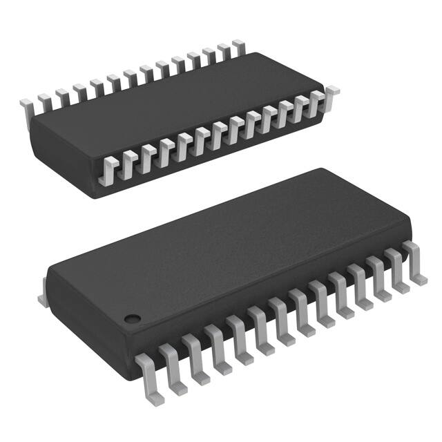
28-pin (300 mil and 330 mil) SOIC packages
■
RoHS compliance
N
In ot r
pr ec
od om
uc m
tio en
n de
to d
su fo
pp r n
or ew
to d
ng es
oi ig
ng ns
pr .
od
uc
tio
n
pr
og
ra
m
s
on
l
y.
Features
Logic Block Diagram
Cypress Semiconductor Corporation
Document Number: 001-50591 Rev. *A
•
198 Champion Court
•
San Jose, CA 95134-1709
•
408-943-2600
Revised December 11, 2009
[+] Feedback
�STK11C88
Contents
pr
og
ra
m
s
on
l
y.
Capacitance ........................................................................ 8
Thermal Resistance ............................................................ 8
AC Test Conditions ............................................................ 8
AC Switching Characteristics ........................................... 9
SRAM Read Cycle ........................................................ 9
Switching Waveforms ........................................................ 9
SRAM Write Cycle....................................................... 10
Switching Waveforms ...................................................... 10
STORE INHIBIT or Power Up RECALL ........................... 11
Switching Waveforms ...................................................... 11
Software Controlled STORE/RECALL Cycle .................. 12
Switching Waveforms ...................................................... 12
Part Numbering Nomenclature ........................................ 13
Ordering Information ........................................................ 13
Package Diagrams ............................................................ 14
Document History Page ................................................... 16
Sales, Solutions and Legal Information ......................... 16
Worldwide Sales and Design Support......................... 16
Products ...................................................................... 16
N
In ot r
pr ec
od om
uc m
tio en
n de
to d
su fo
pp r n
or ew
to d
ng es
oi ig
ng ns
pr .
od
uc
tio
n
Features ............................................................................... 1
Functional Description ....................................................... 1
Logic Block Diagram .......................................................... 1
Contents .............................................................................. 2
Pin Configurations ............................................................. 3
Device Operation ................................................................ 4
SRAM Read ......................................................................... 4
SRAM Write ......................................................................... 4
Software STORE ................................................................. 4
Software RECALL ............................................................... 4
Hardware RECALL (Power Up) .......................................... 4
Hardware Protect ................................................................ 5
Noise Considerations ......................................................... 5
Low Average Active Power ................................................ 5
Best Practices ..................................................................... 5
Maximum Ratings ............................................................... 7
Operating Range ................................................................. 7
DC Electrical Characteristics ............................................ 7
Data Retention and Endurance ......................................... 7
Document Number: 001-50591 Rev. *A
Page 2 of 16
[+] Feedback
�STK11C88
Pin Configurations
$��
�
��
9&&
$��
$�
�
��
�
��
:(
$ ��
$�
�
$�
$�
$�
�
��
��
�
��
�
��
$�
�
��
2(
$��
$�
�
��
&(
��
'4�
on
l
$�
��
��
��
'4�
'4�
'4�
��
��
��
��
'4�
'4�
966
��
��
'4�
m
ra
og
N
In ot r
pr ec
od om
uc m
tio en
n de
to d
su fo
pp r n
or ew
to d
ng es
oi ig
ng ns
pr .
od
uc
tio
n
$�
'4�
s
$�
$��
pr
�723�
y.
Figure 1. Pin Diagram - 28-Pin SOIC
Table 1. Pin Definitions - 28-Pin SOIC
Pin Name
Alt
I/O Type
A0–A14
Input
DQ0-DQ7
Input or
Output
WE
CE
OE
VSS
VCC
Description
Address Inputs. Used to select one of the 32,768 bytes of the nvSRAM.
Bidirectional Data I/O lines. Used as input or output lines depending on operation.
W
Input
Write Enable Input, Active LOW. When the chip is enabled and WE is LOW, data on the
I/O pins is written to the specific address location.
E
Input
Chip Enable Input, Active LOW. When LOW, selects the chip. When HIGH, deselects the
chip.
G
Input
Output Enable, Active LOW. The active LOW OE input enables the data output buffers
during read cycles. Deasserting OE HIGH causes the I/O pins to tristate.
Ground
Ground for the Device. The device is connected to the ground of the system.
Power Supply Power Supply Inputs to the Device.
Document Number: 001-50591 Rev. *A
Page 3 of 16
[+] Feedback
�STK11C88
y.
on
l
s
Data is transferred from the nonvolatile memory to the SRAM
by a software address sequence. A software RECALL cycle is
initiated with a sequence of READ operations in a manner
similar to the software STORE initiation. To initiate the
RECALL cycle, the following sequence of CE controlled READ
operations is performed:
1. Read address 0x0E38, Valid READ
2. Read address 0x31C7, Valid READ
3. Read address 0x03E0, Valid READ
4. Read address 0x3C1F, Valid READ
5. Read address 0x303F, Valid READ
6. Read address 0x0C63, Initiate RECALL cycle
N
In ot r
pr ec
od om
uc m
tio en
n de
to d
su fo
pp r n
or ew
to d
ng es
oi ig
ng ns
pr .
od
uc
tio
n
SRAM Write
Software RECALL
m
The STK11C88 performs a READ cycle whenever CE and OE
are LOW, while WE is HIGH. The address specified on pins
A0–14 determines the 32,768 data bytes accessed. When the
READ is initiated by an address transition, the outputs are
valid after a delay of tAA (READ cycle 1). If the READ is
initiated by CE or OE, the outputs are valid at tACE or at tDOE,
whichever is later (READ cycle 2). The data outputs
repeatedly respond to address changes within the tAA access
time without the need for transitions on any control input pins,
and remain valid until another address change or until CE or
OE is brought HIGH.
The software sequence is clocked with CE controlled READs.
When the sixth address in the sequence is entered, the
STORE cycle commences and the chip is disabled. It is
important that READ cycles and not WRITE cycles are used
in the sequence. It is not necessary that OE is LOW for a valid
sequence. After the tSTORE cycle time is fulfilled, the SRAM is
again activated for READ and WRITE operation.
ra
SRAM Read
og
The STK11C88 is a versatile memory chip that provides
several modes of operation. The STK11C88 can operate as a
standard 32K x 8 SRAM. A 32K x 8 array of nonvolatile storage
elements shadow the SRAM. SRAM data can be copied from
nonvolatile memory or nonvolatile data can be recalled to the
SRAM.
1. Read address 0x0E38, Valid READ
2. Read address 0x31C7, Valid READ
3. Read address 0x03E0, Valid READ
4. Read address 0x3C1F, Valid READ
5. Read address 0x303F, Valid READ
6. Read address 0x0FC0, Initiate STORE cycle
pr
Device Operation
A WRITE cycle is performed whenever CE and WE are LOW.
The address inputs must be stable prior to entering the WRITE
cycle and must remain stable until either CE or WE goes HIGH
at the end of the cycle. The data on the common I/O pins
DQ0–7 are written into the memory if it has valid tSD, before the
end of a WE controlled WRITE or before the end of an CE
controlled WRITE. Keep OE HIGH during the entire WRITE
cycle to avoid data bus contention on common I/O lines. If OE
is left LOW, internal circuitry turns off the output buffers tHZWE
after WE goes LOW.
Software STORE
Data is transferred from the SRAM to the nonvolatile memory
by a software address sequence. The STK11C88 software
STORE cycle is initiated by executing sequential CE controlled
READ cycles from six specific address locations in exact
order. During the STORE cycle, an erase of the previous
nonvolatile data is first performed, followed by a program of
the nonvolatile elements. When a STORE cycle is initiated,
input and output are disabled until the cycle is completed.
Because a sequence of READs from specific addresses is
used for STORE initiation, it is important that no other READ
or WRITE accesses intervene in the sequence. If they
intervene, the sequence is aborted and no STORE or RECALL
takes place.
To initiate the software STORE cycle, the following READ
sequence is performed:
Document Number: 001-50591 Rev. *A
Internally, RECALL is a two step procedure. First, the SRAM
data is cleared, and then the nonvolatile information is transferred into the SRAM cells. After the tRECALL cycle time, the
SRAM is once again ready for READ and WRITE operations.
The RECALL operation does not alter the data in the nonvolatile elements. The nonvolatile data can be recalled an
unlimited number of times.
Hardware RECALL (Power Up)
During power up or after any low power condition
(VCC VIH
tRC=45ns, CE > VIH
m
Test Conditions
og
Description
Average VCC Current tRC = 25 ns
tRC = 45 ns
Dependent on output loading and cycle rate.
Values obtained without output loads.
IOUT = 0 mA.
pr
Parameter
ICC1
s
Over the operating range (VCC = 4.5V to 5.5V)
VCC Standby Current CE > (VCC – 0.2V). All others VIN < 0.2V or > (VCC – 0.2V).
(Standby, Stable
CMOS Input Levels)
IIX
IOZ
VIH
VIL
VOH
Input Leakage
Current
VCC = Max, VSS < VIN < VCC
-1
+1
μA
Off State Output
Leakage Current
VCC = Max, VSS < VIN < VCC, CE or OE > VIH or WE < VIL
-5
+5
μA
Input HIGH Voltage
2.2
VCC +
0.5
V
Input LOW Voltage
VSS –
0.5
0.8
V
0.4
V
Output HIGH Voltage IOUT = –4 mA
VOL
Output LOW Voltage IOUT = 8 mA
2.4
V
Data Retention and Endurance
Parameter
Description
DATAR
Data Retention
NVC
Nonvolatile STORE Operations
Min
Unit
100
Years
1,000
K
Note
3. CE > VIH will not produce standby current levels until any nonvolatile cycle in progress has timed out.
Document Number: 001-50591 Rev. *A
Page 7 of 16
[+] Feedback
�STK11C88
Capacitance
In the following table, the capacitance parameters are listed.[4]
Parameter
Description
CIN
Input Capacitance
COUT
Output Capacitance
Test Conditions
Max
Unit
5
pF
7
pF
TA = 25°C, f = 1 MHz,
VCC = 0 to 3.0 V
Thermal Resistance
In the following table, the thermal resistance parameters are listed.[4]
Thermal Resistance
(Junction to Case)
TBD
TBD
°C/W
TBD
°C/W
y.
TBD
Unit
on
l
Test conditions follow standard test methods and
procedures for measuring thermal impedance,
per EIA / JESD51.
28-SOIC
(330 mil)
s
Thermal Resistance
(Junction to Ambient)
m
ΘJC
28-SOIC
(300 mil)
ra
ΘJA
Test Conditions
Description
og
Parameter
pr
Figure 4. AC Test Loads
N
In ot r
pr ec
od om
uc m
tio en
n de
to d
su fo
pp r n
or ew
to d
ng es
oi ig
ng ns
pr .
od
uc
tio
n
R1 480Ω
5.0V
Output
30 pF
R2
255Ω
AC Test Conditions
Input Pulse Levels .................................................. 0 V to 3 V
Input Rise and Fall Times (10% - 90%)........................


 工商网监
湘ICP备2023018690号
工商网监
湘ICP备2023018690号
