STK16C88
256 Kbit (32K x 8) AutoStore+ nvSRAM
Functional Description
■
25 ns and 45 ns access times
■
Directly replaces battery-backed SRAM modules such as
Dallas/Maxim DS1230 AB
■
Automatic nonvolatile STORE on power loss
■
Nonvolatile STORE under Software control
■
Automatic RECALL to SRAM on power up
■
Unlimited Read/Write endurance
■
Unlimited RECALL cycles
The Cypress STK16C88 is a 256 Kb fast static RAM with a
nonvolatile element in each memory cell. The embedded
nonvolatile elements incorporate QuantumTrap technology
producing the world’s most reliable nonvolatile memory. The
SRAM provides unlimited read and write cycles, while
independent, nonvolatile data resides in the highly reliable
QuantumTrap cell. Data transfers from the SRAM to the
nonvolatile elements (the STORE operation) takes place
automatically at power down. On power up, data is restored to
the SRAM (the RECALL operation) from the nonvolatile
memory. Both the STORE and RECALL operations are also
available under software control.
■
1,000,000 STORE cycles
■
100 year data retention
■
Single 5V+10% power supply
■
Commercial and Industrial Temperatures
■
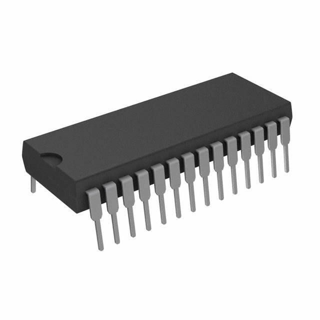
28-pin (600 mil) PDIP package
■
RoHS compliance
In ot r
pr ec
od om
uc m
tio en
n de
to d
su fo
pp r n
or ew
to d
ng es
oi ig
ng ns
pr .
od
uc
tio
n
pr
og
ra
m
s.
Features
N
Logic Block Diagram
Cypress Semiconductor Corporation
Document Number: 001-50595 Rev. *B
•
198 Champion Court
•
San Jose, CA 95134-1709
•
408-943-2600
Revised October 8, 2010
[+] Feedback
�STK16C88
Contents
n
pr
og
ra
m
s.
DC Electrical Characteristics ............................................. 7
Data Retention and Endurance .......................................... 7
Capacitance ......................................................................... 8
Thermal Resistance............................................................. 8
AC Test Conditions ............................................................. 8
AC Switching Characteristics ............................................ 9
Switching Waveforms ......................................................... 9
AutoStore or Power Up RECALL ..................................... 11
Software Controlled STORE/RECALL Cycle................... 12
Part Numbering Nomenclature
(Commercial and Industrial) ............................................. 13
Ordering Information......................................................... 13
Package Diagrams............................................................. 14
Sales, Solutions and Legal Information .......................... 15
Worldwide Sales and Design Support .......................... 15
Products ....................................................................... 15
tio
1
1
1
2
3
4
4
4
4
4
4
4
5
5
5
5
7
N
In ot r
pr ec
od om
uc m
tio en
n de
to d
su fo
pp r n
or ew
to d
ng es
oi ig
ng ns
pr .
od
uc
Features................................................................................
Functional Description........................................................
Logic Block Diagram...........................................................
Contents ...............................................................................
Pin Configurations ..............................................................
Device Operation .................................................................
SRAM Read ..........................................................................
SRAM Write ..........................................................................
AutoStore+ Operation .........................................................
Hardware RECALL (Power Up)...........................................
Software STORE ..................................................................
Software RECALL................................................................
Hardware Protect.................................................................
Noise Considerations..........................................................
Low Average Active Power.................................................
Best Practices......................................................................
Maximum Ratings................................................................
Document Number: 001-50595 Rev. *B
Page 2 of 15
[+] Feedback
�STK16C88
Pin Configurations
Figure 1. Pin Diagram - 28-Pin PDIP
$��
�
��
9&&
$��
$�
�
��
�
��
:(
$ ��
$�
�
$�
$�
$�
�
��
��
�
��
�
��
$�
�
��
2(
$��
$�
�
��
&(
$�
��
'4�
��
��
'4�
'4�
'4�
��
��
��
��
pr
og
��
'4�
��
n
'4�
'4�
tio
In ot r
pr ec
od om
uc m
tio en
n de
to d
su fo
pp r n
or ew
to d
ng es
oi ig
ng ns
pr .
od
uc
966
s.
$�
$��
ra
m
�723�
$�
��
'4�
Table 1. Pin Definitions - 28-Pin PDIP
Pin Name
Alt
A0–A14
I/O Type
Input
DQ0-DQ7
Input or
Output
W
CE
E
OE
G
VSS
VCC
Bidirectional Data I/O lines. Used as input or output lines depending on operation.
Input
Write Enable Input, Active LOW. When the chip is enabled and WE is LOW, data on the
I/O pins is written to the specific address location.
Input
Chip Enable Input, Active LOW. When LOW, selects the chip. When HIGH, deselects the
chip.
Input
Output Enable, Active LOW. The active LOW OE input enables the data output buffers
during read cycles. Deasserting OE HIGH causes the I/O pins to tristate.
N
WE
Description
Address Inputs. Used to select one of the 32,768 bytes of the nvSRAM.
Ground
Ground for the Device. The device is connected to ground of the system.
Power Supply Power Supply Inputs to the Device.
Document Number: 001-50595 Rev. *B
Page 3 of 15
[+] Feedback
�STK16C88
Because a sequence of READs from specific addresses is
used for STORE initiation, it is important that no other READ
or WRITE accesses intervene in the sequence. If they
intervene, the sequence is aborted and no STORE or RECALL
takes place.
To initiate the software STORE cycle, the following READ
sequence is performed:
1. Read address 0x0E38, Valid READ
2. Read address 0x31C7, Valid READ
3. Read address 0x03E0, Valid READ
4. Read address 0x3C1F, Valid READ
5. Read address 0x303F, Valid READ
6. Read address 0x0FC0, Initiate STORE cycle
pr
The STK16C88 performs a READ cycle whenever CE and OE
are LOW while WE is HIGH. The address specified on pins
A0–14 determines the 32,768 data bytes accessed. When the
READ is initiated by an address transition, the outputs are
valid after a delay of tAA (READ cycle 1). If the READ is
initiated by CE or OE, the outputs are valid at tACE or at tDOE,
whichever is later (READ cycle 2). The data outputs
repeatedly respond to address changes within the tAA access
time without the need for transitions on any control input pins,
and remains valid until another address change or until CE or
OE is brought HIGH.
Data is transferred from the SRAM to the nonvolatile memory
by a software address sequence. The STK16C88 software
STORE cycle is initiated by executing sequential CE controlled
READ cycles from six specific address locations in exact
order. During the STORE cycle, an erase of the previous
nonvolatile data is first performed followed by a program of the
nonvolatile elements. When a STORE cycle is initiated, input
and output are disabled until the cycle is completed.
s.
SRAM Read
Software STORE
ra
m
The AutoStore+ STK16C88 is a fast 32K x 8 SRAM that does
not lose its data on power down. The data is preserved in
integral QuantumTrap nonvolatile storage elements when
power is lost. Automatic STORE on power down and
automatic RECALL on power up guarantee data integrity
without the use of batteries.
If the STK16C88 is in a WRITE state at the end of power up
RECALL, the SRAM data is corrupted. To help avoid this
situation, a 10 Kohm resistor is connected either between WE
and system VCC or between CE and system VCC.
og
Device Operation
In ot r
pr ec
od om
uc m
tio en
n de
to d
su fo
pp r n
or ew
to d
ng es
oi ig
ng ns
pr .
od
uc
A WRITE cycle is performed whenever CE and WE are LOW.
The address inputs must be stable prior to entering the WRITE
cycle and must remain stable until either CE or WE goes HIGH
at the end of the cycle. The data on the common I/O pins
DQ0–7 are written into the memory if it has valid tSD, before the
end of a WE controlled WRITE or before the end of an CE
controlled WRITE. Keep OE HIGH during the entire WRITE
cycle to avoid data bus contention on common I/O lines. If OE
is left LOW, internal circuitry turns off the output buffers tHZWE
after WE goes LOW.
tio
n
SRAM Write
AutoStore+ Operation
The STK16C88’s automatic STORE on power down is completely transparent to the system. The STORE initiation takes
less than 500 ns when power is lost (VCC < VSWITCH) at which
point the part depends only on its internal capacitor for
STORE completion.
N
If the power supply drops faster than 20 μs/volt before Vcc
reaches Vswitch, then a 2.2 ohm resistor should be inserted
between Vcc and the system supply to avoid a momentary
excess of current between Vcc and internal capacitor.
In order to prevent unneeded STORE operations, automatic
STOREs are ignored unless at least one WRITE operation has
taken place since the most recent STORE or RECALL cycle.
Software initiated STORE cycles are performed regardless of
whether or not a WRITE operation has taken place.
Hardware RECALL (Power Up)
During power up or after any low power condition
(VCC VIH
(Standby, Cycling
tRC=45ns, CE > VIH
TTL Input Levels)
Commercial
30
22
mA
Industrial
31
23
mA
1.5
mA
In ot r
pr ec
od om
uc m
tio en
n de
to d
su fo
pp r n
or ew
to d
ng es
oi ig
ng ns
pr .
od
uc
tio
n
ICC2
VCC Standby Current CE > (VCC – 0.2V). All others VIN < 0.2V or > (VCC – 0.2V).
(Standby, Stable
CMOS Input Levels)
IIX
Input Leakage
Current
VCC = Max, VSS < VIN < VCC
-1
+1
μA
IOZ
Off State Output
Leakage Current
VCC = Max, VSS < VIN < VCC, CE or OE > VIH or WE < VIL
-5
+5
μA
VIH
Input HIGH Voltage
2.2
VCC +
0.5
V
VIL
Input LOW Voltage
VSS –
0.5
0.8
V
VOH
Output HIGH Voltage IOUT = –4 mA
VOL
Output LOW Voltage IOUT = 8 mA
N
ISB2[3]
2.4
V
0.4
V
Data Retention and Endurance
Parameter
Description
DATAR
Data Retention
NVC
Nonvolatile STORE Operations
Min
Unit
100
Years
1,000
K
Note
3. CE > VIH does not produce standby current levels until any nonvolatile cycle in progress has timed out.
Document Number: 001-50595 Rev. *B
Page 7 of 15
[+] Feedback
�STK16C88
Capacitance
In the following table, the capacitance parameters are listed.[4]
Parameter
Description
CIN
Input Capacitance
COUT
Output Capacitance
Test Conditions
TA = 25°C, f = 1 MHz,
VCC = 0 to 3.0 V
Max
Unit
5
pF
7
pF
Thermal Resistance
In the following table, the thermal resistance parameters are listed.[4]
ΘJA
ΘJC
Description
Thermal Resistance
(Junction to Ambient)
Thermal Resistance
(Junction to Case)
Test Conditions
28-PDIP
Unit
Test conditions follow standard test methods and procedures for measuring thermal impedance, per EIA /
JESD51.
TBD
°C/W
TBD
°C/W
s.
Parameter
og
ra
m
Figure 4. AC Test Loads
pr
R1 480Ω
tio
n
5.0V
In ot r
pr ec
od om
uc m
tio en
n de
to d
su fo
pp r n
or ew
to d
ng es
oi ig
ng ns
pr .
od
uc
Output
30 pF
R2
255Ω
AC Test Conditions
N
Input Pulse Levels .................................................. 0 V to 3 V
Input Rise and Fall Times (10% - 90%)........................