物料型号:
- LM1117系列
器件简介:
- LM1117系列是低压差、1A输出电流的正电压调节器,可以提供高达1A的输出电流,内部电路设计使得输入输出压差最低可达1.4V。该系列产品适用于低电压IC应用,例如高速总线终端和低电流3.3V逻辑电源供应,也适用于VGA卡等其他应用。
引脚分配:
- ADJ/GND(1脚)
- OUTPUT(2脚)
- INPUT(3脚)
参数特性:
- 可调或固定输出
- 最大输出电流1A,最低输入输出压差1.4V
- 良好的噪声抑制
- 内置过热保护
- 快速瞬态响应
功能详解:
- LM1117系列包括可调输出和固定输出两种版本,可为低电压IC应用提供稳定的电源供应。
- 固定电压调节器和可调电压调节器的典型应用数据图。
- 电气特性包括参考电压、输出电压、线路调整率、负载调整率、压差电压、电流限制、最小负载电流、调整引脚电流、静态电流等。
应用信息:
- 高效率线性调节器
- 电线逻辑调节器
- 可调电源
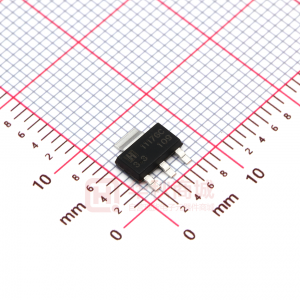
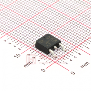
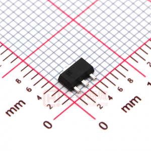
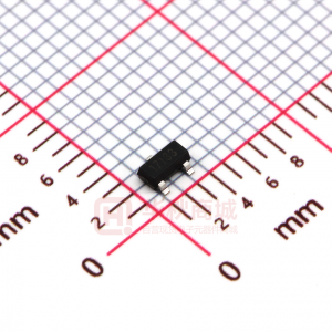
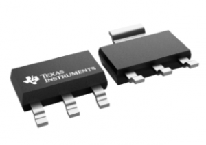
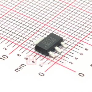
封装信息:
- TO-252封装
- 3引脚TO-252塑料表面贴装封装
- 封装尺寸和公差信息
物料材质:
- 铅:42合金;焊料镀层
- 模具化合物:环氧树脂家族,UL94V-0易燃固体燃烧等级