0
登录后你可以
  • 下载海量资料
  • 学习在线课程
  • 观看技术视频
  • 写文章/发帖/加入社区
会员中心
创作中心
发布
  • 发文章

  • 发资料

  • 发帖

  • 提问

  • 发视频

创作活动
SMCJ100C

SMCJ100C

  • 厂商:

    DAESAN(DAESAN)

  • 封装:

  • 描述:

    SMCJ100C - POWER 1500Watts VOLTAGE 5.0 to 188 Volts - Daesan Electronics Corp.

  • 详情介绍
  • 数据手册
  • 价格&库存
SMCJ100C 数据手册
SMCJ5.0 THRU SMCJ188CA Features · Underwriters Laboratory recognition under UL standard for safety 497B : Isolated loop curcuit protection · Low profile package with built-in strain relief for surface mounted applications · Glass passivated junction · Low incremental surge resistance, excellent clamping capability · 1500W peak pulse power capability with a 10/1000μS waveform, repetition rate(duty cycle) : 0.01% · Very fast response time · High temperature soldering guaranteed : 250℃/10 seconds at terminals POWER 1500Watts VOLTAGE 5.0 to 188 Volts DO-214AB (SMC) 0.124(3.15) 0.108(2.75) 0.245(6.22) 0.220(5.59) 0.280(7.11) 0.260(6.60) 0.012(0.31) 0.006(0.15) 0.103(2.62) 0.079(2.00) 0.050(1.27) 0.030(0.76) 0.008(0.203) MAX. 0.320(8.13) 0.305(7.75) Mechanical Data · Case : JEDEC DO-214AB(SMC) molded plastic over passivated chip · Terminals : Solder plated , solderable per MIL-STD-750, method 2026 · Polarity : For uni-directional types the band denotes the cathode, which is positive with respect to the anode under normal TVS operation · Mounting Position : Any · Weight : 0.007 ounce, 0.25 gram Dimensions in inches and (millimeters) Devices For Bidirectional Applications · For bi-directional devices, use suffix C or CA (e.g. SMCJ10C, SMCJ10CA). Electrical characteristics apply in both directions. Maximum Ratings And Electrical Characteristics (Ratings at 25℃ ambient temperature unless otherwise specified) Symbols Peak pulse power dissipation with a 10/1000μS waveform (Note 1,2) Peak pulse current with a waveform (Note 1) Peak forward surge current, 8.3mm single half sine-wave unidirectional only (Note 2) Typical thermal resistance, junction to ambient (Note 3) Typical thermal resistance, junction to lead Operating junction and storage temperature range PPPM IPPM IFSM Values Minimum 1500 See next table 200 75 15 -55 to +150 Units Watts Amps Amps ℃/W ℃/W ℃ RθJA RθJL TJ,TSTG Notes: (1) Non repetitive current pulse, per Fig.3 and derated above TA=25℃ per Fig.2 (2) Mounted on 0.31×0.31"(8.0×8.0mm) copper pads to each terminal (3) Mounted on minimum recommended pad layout ELECTRICAL CHARACTERISTIC Ratings at 25℃ ambient temperature unless otherwise specified. VF=3.5V at IF=100A (uni-directional only) Device Type S MC J 5.0(C ) S MC J 5.0(C )A(5) S MC J 6.0(C ) S MC J 6.0(C )A S MC J 6.5(C ) S MC J 6.5(C )A S MC J 7.0(C ) S MC J 7.0(C )A S MC J 7.5(C ) S MC J 7.5(C )A S MC J 8.0(C ) S MC J 8.0(C )A S MC J 8.5(C ) S MC J 8.5(C )A S MC J 9.0(C ) S MC J 9.0(C )A S MC J 10(C ) S MC J 10(C )A S MC J 11(C ) S MC J 11(C )A S MC J 12(C ) S MC J 12(C )A S MC J 13(C ) S MC J 13(C )A S MC J 14(C ) S MC J 14(C )A S MC J 15(C ) S MC J 15(C )A S MC J 16(C ) S MC J 16(C )A S MC J 17(C ) S MC J 17(C )A S MC J 18(C ) S MC J 18(C )A S MC J 20(C ) S MC J 20(C )A S MC J 22(C ) S MC J 22(C )A S MC J 24(C ) S MC J 24(C )A S MC J 26(C ) S MC J 26(C )A S MC J 28(C ) S MC J 28(C )A S MC J 30(C ) S MC J 30(C )A Notes : (1) (2) (3) (4) (5) Device Marking Code UNI BI G DD G DD G DE G DE G DF G DF G DG G DG G DH B DH G DK B DK G DL G DL G DM G DM G DN B DN G DP B DP G DQ B DG G DR B DR G DS B DS G DT B DT G DU B DU G DV B DV G DW B DW G DX B DX G DY G DY G DZ G DZ GE D BE D GE E BE E GE F GE F GE G GE G GE H BE H GE K BE K GE L BE L GE M BE M GE N GE N GE P GE P GE Q GE Q GE R GE R GE S BE S GE T BE T GE U BE U GE V BE V GE W BE W GE X BE X GE Y BE Y GE Z BE Z GFD BFD GFE BFE GFF BFF GFG BFG GFH BFH GFK BFK Breakdown Voltage V(BR) at I T (1) (V) Min Max 6.40 7.82 6.40 7.07 6.67 8.15 6.67 7.37 7.22 8.82 7.22 7.98 7.78 9.51 7.78 8.60 8.33 10.2 8.33 9 .21 8.89 10.9 8.89 9.83 9.44 11.5 9.44 10.4 10.0 12.2 10.0 11.1 11.1 13.6 11.1 12.3 12.2 14.9 12.2 13.5 13.3 16.3 13.3 14.7 14.4 17.6 14.4 15.9 15.6 19.1 15.6 17.2 16.7 20.4 16.7 18.5 17.8 21.8 17.8 19.7 18.9 23.1 18.9 20.9 20.0 24.4 20.0 22.1 22.2 27.1 22.2 24.5 24.4 29.8 24.4 26.9 26.7 32.6 26.7 29.5 28.9 35.3 28.9 31.9 31.1 38.0 31.1 34.4 33.3 40.7 33.3 36.8 Test Current I T (mA) 10.0 10.0 10.0 10.0 10.0 10.0 10.0 10.0 1.0 1.0 1.0 1.0 1.0 1.0 1.0 1.0 1.0 1.0 1.0 1.0 1.0 1.0 1.0 1.0 1.0 1.0 1.0 1.0 1.0 1.0 1.0 1.0 1.0 1.0 1.0 1.0 1.0 1.0 1.0 1.0 1.0 1.0 1.0 1.0 1.0 1.0 Stand-off Voltage VWM (V) 5.0 5.0 6.0 6.0 6.5 6.5 7.0 7.0 7.5 7.5 8.0 8.0 8.5 8.5 9.0 9.0 10 10 11 11 12 12 13 13 14 14 15 15 16 16 17 17 18 18 20 20 22 22 24 24 26 26 28 28 30 30 Maximum Maximum Maximum Reverse Leakage Peak Pulse Surge Clamping at V WM Current I PPM Voltage at I PPM ID ( A) (3) μ (A) (2) VC (V) 1000 156.3 9.6 1000 163.0 9.2 1000 131.6 11.4 1000 145.6 10.3 500 122.0 12.3 500 133.9 11.2 200 112.8 13.3 200 125.0 12.0 100 104.9 14.3 100 116.3 12.9 50 100.0 15.0 50 110.3 13.6 20 94.3 15.9 20 104.2 14.4 10 88.8 16.9 10 97.4 15.4 5.0 79.8 18.8 5.0 88.2 17.0 5.0 74.6 20.1 5.0 82.4 18.2 5.0 68.2 22.0 5.0 75.4 19.9 1.0 63.0 23.8 1.0 69.8 21.5 1.0 58.1 25.8 1.0 64.7 23.2 1.0 55.8 26.9 1.0 61.5 24.4 1.0 52.1 28.8 1.0 57.7 26.0 1.0 49.2 30.5 1.0 54.3 27.6 1.0 46.6 32.2 1.0 51.4 29.2 1.0 41.9 35.8 1.0 46.3 32.4 1.0 38.1 39.4 1.0 42.3 35.5 1.0 34.9 43.0 1.0 38.6 38.9 1.0 32.2 46.6 1.0 35.6 42.1 1.0 30.0 50.0 1.0 33.0 45.4 1.0 28.0 53.5 1.0 31.0 48.4 P uls e tes t: tp 5 0ms S urge current wa ve for m per F ig. 3 and derate per F ig. 2 F or bi-directional types ha ving V WM of 10 V olts and les s , the I D limit is doubled All terms and s ymbols are cons is tent with ANS I/IE E E C 62.35 F or the bi-directional S MC G /S MC J 5.0C A, the maximum V (B R ) is 7.25V ELECTRICAL CHARACTERISTIC Ratings at 25℃ ambient temperature unless otherwise specified. VF=3.5V at IF=100A (uni-directional only) Device Type S MC J 33(C ) S MC J 33(C )A S MC J 36(C ) S MC J 36(C )A S MC J 40(C ) S MC J 40(C )A S MC J 43(C ) S MC J 43(C )A S MC J 45(C ) S MC J 45(C )A S MC J 48(C ) S MC J 48(C )A S MC J 51(C ) S MC J 51(C )A S MC J 54(C ) S MC J 54(C )A S MC J 58(C ) S MC J 58(C )A S MC J 60(C ) S MC J 60(C )A S MC J 64(C ) S MC J 64(C )A S MC J 70(C ) S MC J 70(C )A S MC J 75(C ) S MC J 75(C )A S MC J 78(C ) S MC J 78(C )A S MC J 85(C ) S MC J 85(C )A S MC J 90(C ) S MC J 90(C )A S MC J 100(C ) S MC J 100(C )A S MC J 110(C ) S MC J 110(C )A S MC J 120(C ) S MC J 120(C )A S MC J 130(C ) S MC J 130(C )A S MC J 150(C ) S MC J 150(C )A S MC J 160(C ) S MC J 160(C )A S MC J 170(C ) S MC J 170(C )A S MC J 188(C ) S MC J 188(C )A N otes : (1) (2) (3) (4) Device Marking Code UNI BI GFL BFL GFM BFM GFN BFN GFP BFP GFQ BFQ GFR BFR GFS BFS GFT BFT GFU GFU GFV GFV GFW GFW GFX GFX GFY GFY GFZ GFZ GGD GGD GGE GGE GGF GGF GGG GGG GGH GGH GGK GGK GGL GGL GGM GGM GGN GGN GGP GGP GGQ GGQ GGR GGR GGS GGS GGT GGT GGU GGU GGV GGV GGW GGW GGX GGX GGY GGY GGZ GGZ G HD G HD G HE G HE G HF G HF G HG G HG G HH G HH G HK G HK G HL G HL G HM G HM G HN G HN G HP G HP G HQ G HQ G HR G HR G HT G HT G HS G HS Breakdown Voltage V(BR) at I T (1) (V) Min Max 36.7 44.9 36.7 40.6 40.0 48.9 40.0 44.2 44.4 54.3 44.4 49.1 47.8 58.4 47.8 52.8 50.0 61.1 50.0 55.3 53.3 65.1 53.3 58.9 56.7 69.3 56.7 62.7 60.0 73.3 60.0 66.3 64.4 78.7 64.4 71.2 66.7 81.5 66.7 73.7 71.1 86.9 71.1 78.6 77.8 95.1 77.8 86.0 83.3 102 83.3 92.1 86.7 106 86.7 95.8 94.4 115 94.4 104 100 122 100 111 111 136 111 123 122 149 122 135 133 163 133 147 144 176 144 159 167 204 167 185 178 218 178 197 189 231 189 2 09 209 255 209 231 Test Current I T (mA) 1.0 1.0 1.0 1.0 1.0 1.0 1.0 1.0 1.0 1.0 1.0 1.0 1.0 1.0 1.0 1.0 1.0 1.0 1.0 1.0 1.0 1.0 1.0 1.0 1.0 1.0 1.0 1.0 1.0 1.0 1.0 1.0 1.0 1.0 1.0 1.0 1.0 1.0 1.0 1.0 1.0 1.0 1.0 1.0 1.0 1.0 1.0 1.0 Stand-off Voltage VWM (V) 33 33 36 36 40 40 43 43 45 45 48 48 51 51 54 54 58 58 60 60 64 64 70 70 75 75 78 78 85 85 90 90 100 100 110 110 120 120 130 130 150 150 160 160 170 170 188 188 Maximum Maximum Maximum Reverse Leakage Peak Pulse Surge Clamping at VWM Current I PPM Voltage at I PPM ID ( A) (3) μ (A) (2) VC (V) 1.0 25.4 59.0 1.0 28.1 53.3 1.0 23.3 64.3 1.0 25.8 58.1 1.0 21.0 71.4 1.0 23.3 64.5 1.0 19.6 76.7 1.0 21.6 69.4 1.0 18.7 80.3 1.0 20.6 72.7 1.0 17.5 85.5 1.0 19.4 77.4 1.0 16.5 91.1 1.0 18.2 82.4 1.0 15.6 96.3 1.0 17.2 87.1 1.0 14.6 103 1.0 16.0 93 1.0 14.0 107 1.0 15.5 96 1.0 13.2 114 1.0 14.6 103 1.0 12.0 125 1.0 13.3 113 1.0 11.2 134 1.0 12.4 121 1.0 10.8 139 1.0 11.9 126 1.0 9.9 151 1.0 10.9 137 1.0 9.4 160 1.0 10.3 146 1.0 8.4 179 1.0 9.3 162 1.0 7.7 196 1.0 8.5 177 1.0 7.0 214 1.0 7.8 193 1.0 6.5 231 1.0 7.2 209 1.0 5.6 268 1.0 6.2 243 1.0 5.2 287 1.0 5.8 259 1.0 4.9 304 1.0 5.5 275 1.0 4.4 344 1.0 4.6 328 P uls e tes t: tp = 5 0ms S urge current wa ve for m per F ig. 3 and derate per F ig. 2 F or bi-directional types ha ving V WM of 10 V olts and les s , the I D limit is doubled All terms and s ymbols are cons is tent with ANS I/IE E E C 62.35 RATINGS AND CHARACTERISTIC CURVES SMCJ5.0 THRU SMCJ188CA Fig. 1ÐP eak P uls e P o wer R ating C ur ve P eak P uls e P ower (P P P ) or C urrent (I P P ) Derating in P ercentage, % 100 100 Fig. 2Ð P uls e Derating C ur ve P eak P uls e P ower (kW) 75 10 50 1 0.31 x 0.31" (8.0 x 8.0mm) C opper P ad A reas 0.1 0.1μs 1.0μs 1 0μs 100μs 1 .0ms 10ms P PPM , 25 0 0 25 50 75 100 125 150 175 200 td , P uls e Width (s ec.) TA , A mbient Temperature ( oC ) Fig. 3Ð P uls e W a veform 150 Fig. 4Ð T ypical J unction C apacitance Uni-Directional 20,000 P eak P uls e C urrent, % I R S M 100 P eak V alue IP P M J unction C apacitance (pF ) tr = 10μs T J = 25 C P uls e Width (td) is defined as the point where the peak current decays to 50% of I P P M o 10,000 Meas ured at Z ero B ias 1,000 V R , Meas ured at S tand-Off V oltage, V WM 100 Uni-Directional B i-Directional 10 T J = 25 C f = 1.0MHz V s ig = 50mV p-p 100 400 o Half V alue IP P M 50 IP P 2 10/1000μs W aveform as defined by R .E .A. td IP P M , 0 0 1.0 2.0 3.0 4.0 CJ , 1 10 t, T ime (ms ) V WM , R evers e S tand-Off V oltage (V ) F ig. 5ÐT ypic al T rans ient T hermal I mpedanc e 100 Fig. 6 - Maximum Non-R epetitive Forwar d S urg e C urrent Uni-Directional Us e Onl y 200 T rans ient T hermal Impedance ( oC /W) 10 1.0 P eak F orward S urge C urrent, A mperes 100 0.1 0.001 10 0.01 0.1 1 10 100 1000 8.3ms S ingle Half S ine-W ave (J E DE C Method) T J = T J max. 1 10 100 tp , P uls e Duration (s ec) Number of C ycles at 60Hz
SMCJ100C
### 物料型号 - 型号范围:SMCJ5.0至SMCJ188CA

### 器件简介 - DEC SMCJ系列为瞬态电压抑制二极管(TVS),提供1500W的峰值脉冲功率能力,用于保护电子设备免受电压突波影响。

### 引脚分配 - 器件为单向或双向TVS二极管,单向类型带有一个色环表示阴极,双向类型使用后缀C或CA。

### 参数特性 - 安全认证:符合UL标准497B的安全认证。 - 封装:低剖面封装,适用于表面贴装应用。 - 性能:玻璃钝化结、低增量浪涌电阻、优秀的钳位能力、快速响应时间。 - 功率:1500W峰值脉冲功率能力,10/1000μS波形,重复率(占空比)为0.01%。 - 温度:保证在250℃下10秒的高温焊接。

### 功能详解 - 单向与双向:单向TVS在正常TVS操作下,带色环的为阴极,相对于阳极为正;双向TVS则无此区分。 - 电气特性:包括击穿电压、最大反向漏电流、峰值脉冲浪涌电流、钳位电压等。

### 应用信息 - 主要用于保护电子设备免受静电放电(ESD)、电感性负载开关引起的浪涌、电源和信号线瞬态电压等。

### 封装信息 - 
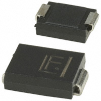
封装类型:JEDEC DO-214AB(SMC)模塑塑料覆盖钝化芯片。 - 端子:端子为镀锡,符合MIL-STD-750, 方法2026的可焊性标准。 - 尺寸:提供英寸和毫米两种单位的尺寸数据。 - 重量:约0.007盎司,0.25克。
SMCJ100C 价格&库存

很抱歉,暂时无法提供与“SMCJ100C”相匹配的价格&库存,您可以联系我们找货

免费人工找货