SCOPE:
IMPROVED, QUAD, SPST ANALOG SWITCHES
Device Type
01
02
03
Generic Number
DG411A(x)/883B
DG412A(x)/883B
DG413A(x)/883B
Case Outline(s). The case outlines shall be designated in Mil-Std-1835 and as follows:
Outline Letter
MAXIM
SMD
K
E
L
X
Z
2
Mil-Std-1835
GDIP1-T16 or CDIP2-T16
CDFP4-F16
CQCC1-N20
Case Outline
Package Code
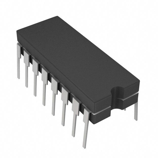
16 LEAD CERDIP
16 LEAD FLATPACK
20-Pin Ceramic LCC
J16
F16
L20
Absolute Maximum Ratings
V+ to V- .............................................................................................................................. 44V
GND to V- ......................................................................................................................... 25V
Logic Supply Voltage (VL) to V- 2/ .................................................... (GND-0.3V) to 44Vdc
Digital Inputs, VS, VD 2/ .................................................................(V -) -2Vdc to (V+) +2Vdc
or 30mA whichever occurs first.
Continuous Current, Any terminal .................................................................................. 30mA
Source or drain Current (Pulsed at 1ms, 10% duty cycle max) .................................... 100mA
Lead Temperature (soldering, 10 seconds) ...............................................................…..... +300°C
Storage Temperature ........................................................................................... -65°C to +150°C
Continuous Power Dissipation .........................................................................…….... TA=+70°C
16 lead CERDIP(derate 10.0mW/°C above +70°C) ...............................................…….. 800mW
16 lead FLATPACK(derate 6.1mW/°C above +70°C) .........................................…….... 485mW
20 lead LCC (derate 9.1 mW/°C above +70°C) ..................................................……..... 727mW
Junction Temperature TJ ....................................................................................………. +150°C
Thermal Resistance, Junction to Case, ΘJC:
Case Outline 16 lead CERDIP...............................................................……..... 50°C/W
Case Outline 16 lead FLATPACK .........................................................……... 65°C/W
Case Outline 20 lead LCC .....................................................................…….... 20°C/W
Thermal Resistance, Junction to Ambient, ΘJA:
Case Outline 16 lead CERDIP.............................................................……..... 100°C/W
Case Outline 16 lead FLATPACK .......................................................……... 165°C/W
Case Outline 20 lead LCC ...................................................................…….... 110°C/W
Recommended Operating Conditions
Ambient Operating Range (TA) ........................................................……….... -55°C to +125°C
Unipolar Supply Voltage (V+) ...............................................................................………….12V
(V-) ................................................................................………….. 0V
Bipolar Supply Voltage (V+) ...............................................................................…………. 15V
(V-) ..............................................................................………….. 15V
Logic Supply Voltage (VL) ....................................................................................…….. +5.25V
NOTE 1: Stresses beyond those listed under “Absolute Maximum Ratings” may cause permanent damage to the
device. These are stress ratings only, and functional operation of the device at these or any other
conditions beyond those indicated in the operational sections of the specifications is not implied.
Exposure to absolute maximum rating conditions for extended periods may affect device reliability.
NOTE 2: Signals on SX, DX or INX exceeding V+ or V- are clamped by internal diodes. Limit forward current to
maximum current ratings.
----------------------------
Electrical Characteristics of DG411A/412A
/413A /883B for SMD 5962-90731
19-0338
Page 2 of
Rev. B
10
�TABLE 1 ELECTRICAL TESTS
TEST
Symbol
Drain-to-Source
ON Resistance
Drain-to-Source
ON Resistance
Source OFF
leakage current
and
Drain OFF
leakage current
Source OFF
leakage current
and
Drain OFF
leakage current
Channel ON
leakage current
rDS(ON)
rDS(ON)
IS(OFF)
and
CONDITIONS
1/
-55 °C
很抱歉,暂时无法提供与“5962-9073103MEA”相匹配的价格&库存,您可以联系我们找货
免费人工找货