71M6515H Demo Board User’s Manual
71M6515H Demo Board
USER’S MANUAL
12/5/2005 2:06 PM
Revision 2.0
TERIDIAN Semiconductor Corporation
6440 Oak Canyon Rd.
Irvine, CA 92618-5201
Phone: (714) 508-8800 ▪ Fax: (714) 508-8878
http://www.teridian.com/
meter.support@teridian.com
Revision 2.0
1 of 66
© Copyright 2005 TERIDIAN Semiconductor Corporation
�71M6515H Demo Board User’s Manual
TERIDIAN Semiconductor Corporation makes no warranty for the use of its products, other than expressly contained in the
Company’s warranty detailed in the TERIDIAN Semiconductor Corporation standard Terms and Conditions. The company assumes
no responsibility for any errors which may appear in this document, reserves the right to change devices or specifications detailed
herein at any time without notice and does not make any commitment to update the information contained herein.
Revision 2.0
2 of 66
© Copyright 2005 TERIDIAN Semiconductor Corporation
�71M6515H Demo Board User’s Manual
71M6515H
3-Phase Power Meter AFE IC
DEMO BOARD
USER’S MANUAL
Revision 2.0
3 of 66
© Copyright 2005 TERIDIAN Semiconductor Corporation
�71M6515H Demo Board User’s Manual
Table of Contents
1
GETTING STARTED .......................................................................................................................................... 7
1.1
General............................................................................................................................................................... 7
1.2
Safety and ESD Notes....................................................................................................................................... 7
1.3
Demo Kit Contents ............................................................................................................................................ 7
1.4
Compatibility Statement ................................................................................................................................... 7
1.5
Suggested Equipment not included ................................................................................................................ 8
1.6
Demo Board Test Setup.................................................................................................................................... 8
1.6.1
Power Supply Setup..................................................................................................................................... 9
1.6.2
Serial Connection Setup ............................................................................................................................ 10
1.7
Preparing the PC ............................................................................................................................................. 10
1.8
Using the Demo Board.................................................................................................................................... 11
1.8.1
Starting up the Demo Board and the GUI Program.................................................................................... 11
1.8.2
Controlling the Demo Board ....................................................................................................................... 11
1.8.3
GUI Window - Overview............................................................................................................................ 12
1.8.4
GUI Window – Display and Control Fields ................................................................................................. 12
1.8.5
GUI Window Control and Display Fields – Detailed Description ................................................................ 14
1.8.6
Adjusting the Kh Factor for the Demo Board.............................................................................................. 24
1.8.7
Adjusting the Demo Boards to Different Current Transformers and Voltage Dividers ................................ 25
1.9
Calibrating the Demo Meter............................................................................................................................ 26
2
APPLICATION INFORMATION........................................................................................................................ 27
2.1
Calibration Procedure..................................................................................................................................... 27
2.1.1
Calibration Systems ................................................................................................................................... 27
2.1.2
Definitions .................................................................................................................................................. 27
2.1.3
Error Sources in a Meter ............................................................................................................................ 28
2.1.4
Calibration with Three Measurements........................................................................................................ 29
2.1.5
Calibration with Five Measurements .......................................................................................................... 30
2.1.6
Calibration for Meters with Rogowski Coil Sensors.................................................................................... 31
2.1.7
Calibration Spreadsheets........................................................................................................................... 32
2.1.8
Compensating for Non-Linearities.............................................................................................................. 33
2.2
Schematic Information.................................................................................................................................... 35
2.2.1
Components for the VFLT Pin.................................................................................................................... 35
2.2.2
Reset Circuit .............................................................................................................................................. 35
2.2.3
Oscillator .................................................................................................................................................... 35
2.3
Testing the Demo Board................................................................................................................................. 37
2.3.1
Testing the Demo Board Using the GUI..................................................................................................... 37
2.3.2
Functional Meter Test ................................................................................................................................ 38
3
HARDWARE DESCRIPTION ........................................................................................................................... 41
3.1
Board Description: Jumpers, Switches and Test Points ............................................................................. 41
3.2
Connector Descriptions.................................................................................................................................. 44
Revision 2.0
4 of 66
© Copyright 2005 TERIDIAN Semiconductor Corporation
�71M6515H Demo Board User’s Manual
3.2.1
3.2.2
3.2.3
JP6 – SSI Interface .................................................................................................................................... 44
JP18 – External Interface........................................................................................................................... 44
JP21 – Debug Interface ............................................................................................................................. 45
3.3
Board Hardware Specifications ..................................................................................................................... 46
4
APPENDIX........................................................................................................................................................ 47
List of Figures
Figure 1-1: TERIDIAN 71M6515H Demo and Debug Boards: Basic Connections......................................................... 8
Figure 1-2: Block diagram for the TERIDIAN 71M6515H Demonstration Meter with Debug Board .............................. 9
Figure 1-3: Control Program Icon................................................................................................................................. 10
Figure 1-4: Host GUI Window w/ Functional Groups (Areas) Marked and Numbered ................................................. 12
Figure 2-1: Phase Angle Definitions............................................................................................................................. 28
Figure 2-2: Watt Meter with Gain and Phase Errors ................................................................................................... 28
Figure 2-3: Calibration Spreadsheet for Three Measurements .................................................................................... 32
Figure 2-4: Calibration Spreadsheet for Five Measurements....................................................................................... 33
Figure 2-5: Non-Linearity Caused by Quantification Noise .......................................................................................... 33
Figure 2-6: Voltage Divider for VFLT ........................................................................................................................... 35
Figure 2-7: External Components for RESETZ ............................................................................................................ 35
Figure 2-8: Oscillator Circuit......................................................................................................................................... 36
Figure 2-9: Typical GUI Window .................................................................................................................................. 37
Figure 2-10: Meter with Calibration System ................................................................................................................. 38
Figure 2-11: Calibration System Screen ...................................................................................................................... 39
Figure 3-1: 71M6515H Demo Board: Connectors, Headers, LEDs, Switches ............................................................. 43
Figure 4-1: TERIDIAN 71M6515H Demo Board: Electrical Schematic 1/3 .................................................................. 48
Figure 4-2: TERIDIAN 71M6515H Demo Board: Electrical Schematic 2/3 .................................................................. 49
Figure 4-3: TERIDIAN 71M6515H Demo Board: Electrical Schematic 3/3 .................................................................. 50
Figure 4-4: TERIDIAN 71M6515H Demo Board: Top View ......................................................................................... 52
Figure 4-5: TERIDIAN 71M6515H Demo Board: Bottom View .................................................................................... 53
Figure 4-6: TERIDIAN 71M6515H Demo Board: Top Signal Layer ............................................................................. 54
Figure 4-7: TERIDIAN 71M6515H Demo Board: Middle Layer 1, Ground Plane. ........................................................ 55
Figure 4-8: TERIDIAN 71M6515H Demo Board: Middle Layer 2, Supply Plane. ......................................................... 56
Figure 4-9: TERIDIAN 71M6515H Demo Board: Bottom Signal Layer ........................................................................ 57
Figure 4-10: Debug Board Schematics ........................................................................................................................ 59
Figure 4-11: Debug Board: Top View........................................................................................................................... 60
Figure 4-12: Debug Board: Bottom View ..................................................................................................................... 60
Figure 4-13: Debug Board: Top Signal Layer............................................................................................................... 61
Figure 4-14: Debug Board: Middle Layer 1, Ground Plane .......................................................................................... 61
Figure 4-15: Debug Board: Middle Layer 2, Supply Plane ........................................................................................... 62
Figure 4-16: Debug Board: Bottom Trace Layer .......................................................................................................... 62
Figure 4-17: TERIDIAN 71M6515H LQFP64: Pinout (top view)................................................................................... 65
Revision 2.0
5 of 66
© Copyright 2005 TERIDIAN Semiconductor Corporation
�71M6515H Demo Board User’s Manual
List of Tables
Table 1-1: Jumper settings on Debug Board................................................................................................................ 10
Table 1-2: Straight cable connections .......................................................................................................................... 10
Table 1-3: Null-modem cable connections ................................................................................................................... 10
Table 3-1: 71M6515H Demo Board Description: 1/3 ................................................................................................... 41
Table 3-2: 71M6515H Demo Board Description: 2/3 ................................................................................................... 42
Table 3-3: 71M6515H Demo Board Description: 3/3 ................................................................................................... 43
Table 3-4: JP6 Pin Description..................................................................................................................................... 44
Table 3-5: JP18 Pin Description (pins 3, 5, 7, 9, and 17 are non-functional) ............................................................... 44
Table 3-6: JP21 Pin Description................................................................................................................................... 45
Table 4-1: 71M6515H Demo Board: Bill of Material..................................................................................................... 51
Table 4-2: Debug Board: Bill of Material ...................................................................................................................... 58
Table 4-3: 71M6515H Pin Description Table 1/2 ......................................................................................................... 63
Table 4-4: 71M6515H Pin Description Table 2/2 ......................................................................................................... 64
Revision 2.0
6 of 66
© Copyright 2005 TERIDIAN Semiconductor Corporation
�71M6515H Demo Board User’s Manual
1
1
GETTING STARTED
1.1
GENERAL
The TERIDIAN Semiconductor Corporation (TSC) 71M6515H Demo Board is a demonstration board for
evaluating the 71M6515H IC for 3-phase electronic power metering applications. It incorporates a
71M6515H integrated circuit, peripheral circuitry such an on-board power supply as well as a companion
Debug Board that allows a connection to a PC running Windows® 2000/XP through a RS232 port. The
demo board allows the evaluation of the 71M6515H power meter controller chip for measurement accuracy
and overall system use.
A control program running on a Windows 2000/XP compatible PC allows control and monitoring of the
71M6515H IC on an abstract level via a graphical user interface (GUI).
1.2
SAFETY AND ESD NOTES
Connecting live voltages to the demo board system will result in potentially hazardous voltages on the demo
board.
EXTREME CAUTION SHOULD BE TAKEN WHEN HANDLING THE DEMO BOARD
ONCE IT IS CONNECTED TO LIVE VOLTAGES!
THE DEMO SYSTEM IS ESD SENSITIVE! ESD PRECAUTIONS SHOULD BE
TAKEN WHEN HANDLING THE DEMO BOARD!
1.3
DEMO KIT CONTENTS
•
71M6515H Demo board containing 71M6515H AFE IC
•
Debug Board
•
Two 5VDC/1,000mA universal wall transformer with 2.5mm plug (Switchcraft 712A compatible)
•
Serial cable, DB9, Male/Female, 2m (Digi-Key AE1020-ND)
•
CD-ROM containing documentation (data sheet, board schematics, BOM, layout), PC executable
program (GUI), and calibration spreadsheet
Note: The media CD-ROM contains a file named readme.txt that specifies all files found on the media and
their purpose.
1.4
COMPATIBILITY STATEMENT
This manual is compatible with REV1.1 (October 14, 2005) of the Control Program (GUI) and with
71M6515H code revision 1.1 (October 14, 2005).
Revision 2.0
7 of 66
© Copyright 2005 TERIDIAN Semiconductor Corporation
�71M6515H Demo Board User’s Manual
1.5
SUGGESTED EQUIPMENT NOT INCLUDED
PC w/ MS-Windows versions XT, ME, or 2000, equipped with RS232 port (COM port) via DB9 connector
1.6
DEMO BOARD TEST SETUP
Figure 1-1 shows the basic connections of the Demo Board plus Debug Board with the external equipment.
Power supply for
Demo Board
Country-specific
plug adapters
(US, Europe,
UK, Australia)
Demo
Board
Power supply
for Debug
Board
Debug
Board
Serial
connection to
PC
Figure 1-1: TERIDIAN 71M6515H Demo and Debug Boards: Basic Connections
The 71M6515H demo board system is shown in Figure 1-2. It consists of a stand-alone rectangular meter
Demo Board and an optional Debug Board (most Debug Boards are partially assembled and have less
components than shown in Figure 1-2). The Demo Board contains all circuits necessary for operation as a
meter front end, calibration LEDs, and power supply. The Debug Board is optically isolated from the meter
and interfaces to a PC through a 9 pin serial port. For serial communication between the PC and the
TERIDIAN 71M6515H, the Debug Board needs to be plugged with its connector J3 into connector JP21 of
the Demo Board.
Connections to the external signals to be measured, i.e. scaled AC voltages and current signals derived
from shunt resistors or current transformers, are provided on the rear side of the demo board.
Note: It is recommended to set up the demo board with no live AC voltage connected, and to
connect live AC voltages only after the user is familiar with the demo system.
Revision 2.0
8 of 66
© Copyright 2005 TERIDIAN Semiconductor Corporation
�71M6515H Demo Board User’s Manual
DEMONSTRATION METER
External Current
Transformers
IA
JP26
IB
JP27
IC
IA
D6
JP30
71M6515H
Single-Chip Meter
AFE
V3P3
D5
WPULSE
V3P3
RPULSE
IB
PULSE3
IC
PULSE4
JP29
External Interface
Connector
JP18
WPULSE
RPULSE
JP28
V3P3
VC
VB
VA
DIO 0...8
JP24
JP23
TX
RX
JP22
VA
VB
VC
JP1
V3P3
JP25
SSI Connector
SSI Signals
JP6
3.3V
NEUTRAL
GND
5V
DC
DEBUG BOARD (OPTIONAL)
GND
S1
TX
OPTO
RX
JP9
JP32
JP31
DB9
to PC
COM Port
RS-232
INTERFACE
OPTO
UARTCSZ
OPTIONAL RTM
INTERFACE
OPTO SUPPLY
TMUXOUT
OPTO
BAUDRATE
CKTEST
OPTO
FPGA
V5_DBG
5V DC
PULSE_INIT
OPTO
SUPPLY
V5_NI
GND_DBG
GND
JP21
Figure 1-2: Block diagram for the TERIDIAN 71M6515H Demonstration Meter with Debug Board
Note: All input signals are referenced to the V3P3 (3.3V power supply to the chip).
1.6.1
POWER SUPPLY SETUP
There are several choices for meter power supply:
•
Internal (using phase A of the AC line voltage). The internal power supply is only suitable when
phase A exceeds 220V RMS.
•
External 5VDC connector (J1) on the Demo Board and external 5VDC connector (J1) on the Debug
Board.
The power supply jumper JP1 must be consistent with the power supply choice. JP1 disconnects phase A
from the power supply. This jumper should usually be left in place.
The internal supply is not strong enough to power the Debug Board. Thus, the external power supply should
always be used for the Debug Board, regardless whether the meter is powered by its internal supply or
through an external supply.
Revision 2.0
9 of 66
© Copyright 2005 TERIDIAN Semiconductor Corporation
�71M6515H Demo Board User’s Manual
1.6.2
SERIAL CONNECTION SETUP
For connection of the DB9 serial port to a PC, either a straight or a so-called “null-modem” cable may be
used. JP1 and JP2 are plugged in for the straight cable, and JP3/JP4 are empty. The jumper configuration is
reversed for the null-modem cable, as shown in Table 1-1.
Configuration
JP1
JP2
JP3
JP4
Straight Cable
installed
installed
--
--
--
--
installed
installed
Null-Modem Cable
Table 1-1: Jumper settings on Debug Board
JP1 through JP4 can also be used to alter the connection when the PC is not configured as a DCE device.
Table 1-2 shows the connections necessary for the straight DB9 cable and the pin definitions.
PC Pin
Function
Demo Board Pin
2
TX
2
3
RX
3
5
Signal Ground
5
Table 1-2: Straight cable connections
Table 1-3 shows the connections necessary for the null-modem DB9 cable and the pin definitions.
PC Pin
Function
Demo Board Pin
2
TX
3
3
RX
2
5
Signal Ground
5
Table 1-3: Null-modem cable connections
1.7
PREPARING THE PC
The Control Program PMtest.exe must be copied from the CD-ROM to a directory on the host PC. The
program can then be started directly by double-clicking on the PMTest.exe icon (see Figure 1-3).
PMTest.exe
Figure 1-3: Control Program Icon
PMTest.exe can work in two baud rates and on any COM port. To configure PMTest.exe for the desired
operation mode, the original PMTest.exe file is copied to or renamed to a file with a name of the form:
PMTestxxxCy.exe
If xxx = 192, the program will operate at 19.2kb/s, if xxx = 384, the program will operate at 38.4kb/s (UART
speed when communicating with the 71M6515H).
The number substituted for y states the COM port number that the program is using for communicating with
the host.
Example: When named PMTest192C2.exe, the program will operate with 19.2kb/s via COM port 2.
Revision 2.0
10 of 66
© Copyright 2005 TERIDIAN Semiconductor Corporation
�71M6515H Demo Board User’s Manual
Note: For smooth operation of the PMTest program it is important to observe the following rules:
•
It is important to exit all programs that access COM port 1 before PMTEST.exe is started.
•
Make sure all applicable updates to the Windows ® operating system are installed before running
the application.
•
PMTest.exe will not run on Windows® 98 or older operating systems.
Real-time performance can be affected by processor-intense operations of the PC, such as starting new
applications, loading files into applications, or ending applications. Such operations have to be avoided to
ensure uninterrupted communication between PC and the 6515H Demo Board.
Do not press the ALT key on the keyboard!
1.8
USING THE DEMO BOARD
The 71M6515H Demo Board is a ready-to-use meter with a preprogrammed scaling factor Kh of 3.2
Wh/pulse. In order to be used with a calibrated load or a meter calibration system, the board should be
connected to the AC power source using the spade terminals on the bottom of the board. The current
transformers should be connected to the dual-pin headers on the bottom of the board. For the Kh to be
adjusted properly, current transformers with 2,000:1 winding ratio must be used.
1.8.1
STARTING UP THE DEMO BOARD AND THE GUI PROGRAM
In order to control and monitor the Demo Board, the connections specified in section 1.6 have to be
established.
The sequence of actions when powering up the Demo Board is as follows:
1.
2.
3.
4.
5.
6.
Power up the Demo Board
Start the GUI Control Program PMTest.exe.
Check for communication between the GUI Control Program and the 71M6515H. Communication is
established when the green “LED” indicator labeled 1SEC on the GUI screen flashes red every
second.
Initialize the 71M6515H to match the desired application and measurement parameters. Establish
the CE image, calibration factors, pulse parameters, nominal temperature, IMAX/VMAX using the
commands and fields described in 1.8.2.
Establish the desired configuration using the bits of the CONFIG register (field 16 in the GUI
window), but do not enable the CE.
Enable the CE by clicking the square button next to “CE_ENABLE”.
Once, voltage is applied and load current is flowing, the red LED D5 will flash each time an energy sum of
3.2 Wh is collected.
Similarly, the red LED D6 will flash each time a reactive energy sum of 3.2 VARh is collected.
1.8.2
CONTROLLING THE DEMO BOARD
Upon starting the PMTEST.exe application, the graphical user interface (GUI) of the demo application
shown in Figure 1-4 will be displayed on the screen. The gray boxes are the meter outputs and the white
boxes contain host, i.e. user, inputs.
It is important to enable the computation engine (CE) in order to see activity in the GUI window. You can
check the computation engine (CE) status by verifying the status of the button on the left of CE_ENABLE in
the “Config” block of the GUI. It should display a “1”, as shown in Figure 1-4. If not, the CE can be enabled
by clicking the “0” button to the left of the “CE_ENABLE” text using the left mouse button. Upon clicking, the
“0” will toggle to a “1”, and the green and red indicator lights underneath the “Status/Mask” text will start
blinking.
Revision 2.0
11 of 66
© Copyright 2005 TERIDIAN Semiconductor Corporation
�71M6515H Demo Board User’s Manual
1.8.3
GUI WINDOW - OVERVIEW
5
1
7
6
8
3
2
9
17
16
12
11
10
13
18
14
19
4
15
20
Figure 1-4: Host GUI Window w/ Functional Groups (Areas) Marked and Numbered
1.8.4
GUI WINDOW – DISPLAY AND CONTROL FIELDS
The PMTEST (GUI) window, as shown in Figure 1-4, contains a number of major blocks or areas (Pulse
Source Select, Config, Status/Mask, Calibration Constants, Temperature Compensation, Real-Time Monitor,
Digital I/O, Thresholds and Operating Time). These major blocks (labeled 1 through 12 in Figure 1-4) group
the functionally related buttons and fields together. The elements of the GUI are as follows:
•
Rectangular buttons: Buttons that can be clicked by the user to initiate an action.
•
Square buttons: Buttons that can be clicked by the user to initiate an action. The square buttons have
a single digit showing the current state of the signal. A “1” is on and a “0” is off.
•
Entry fields: White rectangular fields that can be edited by the user. The delete key plus the number
and cursor keys work in this type of field.
Revision 2.0
12 of 66
© Copyright 2005 TERIDIAN Semiconductor Corporation
�71M6515H Demo Board User’s Manual
•
Display fields: Gray rectangular fields that indicate settings, measurements etc. of the 6515H chip.
These fields cannot be edited by the user.
•
List fields: Entry fields that allow selection from the pre-determined list of choices once the downpointing arrow is pressed (“pull-down” menus).
•
Indicator lights: Red and green activity indicators underneath the “Status/Mask” label.
Green lights mean no activity. Red lights mean that the corresponding bit in
the STATUS mask is set, i.e. the condition is true.
With an input signal (phase A, B, C voltage) present, the F0 light will be on
indicating that the square wave following the input signal is being
generated. The light at “1SEC” will blink red every second. Other lights will
stay green until the corresponding condition is true, e.g. when the input
signal meets a sag or over-voltage threshold.
A summary of all of the GUI window areas follows on the next pages.
Revision 2.0
13 of 66
© Copyright 2005 TERIDIAN Semiconductor Corporation
�71M6515H Demo Board User’s Manual
1.8.5
GUI WINDOW CONTROL AND DISPLAY FIELDS – DETAILED DESCRIPTION
Energy, Voltage/Current and Phase Area (1):
This area is in the upper left corner of the GUI window and contains a number of display fields arranged in
columns. Phase A is the left column, phase B is the center column and phase C is the right column.
Next to the display fields in this area, there are a list field and a rectangular button controlling basic functions
of the Energy, Voltage/Current and Phase Area:
GUI Element (Label)
Element
Type
Function
Accumulated energy,
Instantaneous energy
List field
This control toggles the display of the Wh, VARh and VAh fields
from total accumulated energy to instantaneous energy, i.e.
energy per accumulation interval
CLR ACCUM
Rectangular
button
Resets the accumulators for Wh, VARh and VAh to zero. It also
resets the “Main Edge” counters in the Status/Mask area and the
pulse counters.
The function of the display fields depends on the selected mode, accumulated or instantaneous energy:
GUI Element (Label)
Function – Accumulated Energy
Selected
Function – Instantaneous Energy
Selected
Wh
These fields display the accumulated
energy (real power x time) for each
phase.
These fields display the energy (real
power x time) collected during the last
accumulation interval for each phase.
VARh
These fields display the accumulated
reactive energy (reactive power x
time) for each phase.
These fields display the reactive energy
(reactive power x time) for each phase.
VAh
These fields display the accumulated
apparent energy (apparent power x
time) for each phase.
These fields display the accumulated
apparent energy (apparent power x
time) collected during the last
accumulation interval for each phase.
Vrms
These fields display the momentary voltages (RMS) for each phase.
Irms
These fields display the momentary currents (RMS) for each phase.
Iphase
These fields display the momentary phase angles of the currents for each phase.
VPhase angle
These fields display the momentary phase angles between the phases A and B
(underneath “--- AB ---“) and B and C (underneath “---BC---“).
Gain Adjust
This field displays the current value of the gain adjusted by the temperature
compensation mechanism. It is functionally associated with the fields in area 10.
When no compensation is active, or the temperature deviation is minimal, the
default value of 16384 will be displayed.
Revision 2.0
14 of 66
© Copyright 2005 TERIDIAN Semiconductor Corporation
�71M6515H Demo Board User’s Manual
Calibration Constants Area (2):
This area is on the left side of the GUI window and contains three entry fields for each phase. The function
depends on the selected CE image (CT/Shunt or Rogowski sensor):
GUI Element
(Label)
Function (CT/Shunt)
Calibrate IA
Calibration constant for phase A current (default = 16384)
Function (Rogowski Sensor)
Calibrate VA
Calibration constant for phase A voltage (default = 16384)
Calibrate IB
Calibration constant for phase B current (default = 16384)
Calibrate VB
Calibration constant for phase B voltage (default = 16384)
Calibrate IC
Calibration constant for phase C current (default = 16384)
Calibrate VC
Calibration constant for phase C voltage (default = 16384)
Phase Adjust A
Calibration constant for phase A current
angle (default = 0)
Calibration constant for phase A current
angle (default = -3973)
Phase Adjust B
Calibration constant for phase B current
angle (default = 0)
Calibration constant for phase B current
angle (default = -3973)
Phase Adjust C
Calibration constant for phase C current
angle (default = 0)
Calibration constant for phase C current
angle (default = -3973)
During calibration (see section 2.1), the values of the calibration coefficients obtained with the calibration
formulae should be entered in these fields.
Temperature Compensation Area (3):
This area consists of a vertical column of entry and display fields to the right of the Calibration Constants
area. The Gain Adjust field from area 1 functionally belongs in the Temperature Compensation area.
GUI Element
(Label)
Element
Type
Default
Raw
Display field
--
Raw temperature (chip substrate temperature)
Delta T
Display field
--
Difference between raw and nominal (calibration)
temperature
Nominal
Entry field
0
The raw temperature should be entered here during
calibration
Y Cal deg 0
Entry field
0
The constant correction coefficient for the RTC can be
entered here if RTC compensation is required.
Y Cal deg 1
Entry field
0
The linear correction coefficient for the RTC can be entered
here if RTC compensation is required.
Y Cal deg 2
Entry field
0
The quadratic correction coefficient for the RTC can be
entered here if RTC compensation is required.
Function
PPM/C
Entry field
0
The linear compensation coefficient of gain over
temperature is entered here automatically as soon as a
temperature value is entered in the “Nominal” field.
Values determined by the host may be entered here if
the DEFAULT PPM bit in the Configuration area is set to
0.
PPM/C2
Entry field
0
The quadratic compensation coefficient of gain over
temperature is entered here. See the PPM/C field for details.
DEG SCALE
Entry field
22721
Scaling factor for the calculation of temperature. The default
value for DEG SCALE (22721) should not be changed.
TEMP_X = DEGSCALE * 2-22 * (TEMP_RAW - TEMP_NOM)
Revision 2.0
15 of 66
© Copyright 2005 TERIDIAN Semiconductor Corporation
�71M6515H Demo Board User’s Manual
Rogowski Calibration Area (4):
This area consists of two vertical columns of entry fields in the lower left side of the window. The coefficients
are only active when the Rogowski image is selected for the CE.
GUI Element
(Label)
Default
VFeedA Watt
0
Calibration coefficient for phase A voltage feed through (default = 0)
VFeedB Watt
0
Calibration coefficient for phase B voltage feed through (default = 0)
VFeedC Watt
0
Calibration coefficient for phase C voltage feed through (default = 0)
VFeed A I
0
Not implemented
VFeed B I
0
Not implemented
VFeed C I
0
Not implemented
Function
Pulse Source Selection Area (5):
This area consists of four list fields to the right of the Energy, Voltage/Current and Phase area. The entries
determine the configuration and settings of the two pulse outputs used for four-quadrant metering.
GUI Element
(Label)
Default
Function
Pulse1 Source
Wh
This list field allows selection of internal, external, or one of 35 postprocessed parameters as the source for the PULSEW output.
Pulse2 Source
VARh
This list field allows selection of internal, external, or one of 35 postprocessed parameters as the source for the PULSER output.
Pulse3 Source
Wh
This list field allows selection of either an external (host) input or one of 35
post-processed parameters as the source for the PULSE3 output. The
selection “none” is also available.
When “none” is selected, the pulse output is disabled.
Pulse4 Source
VARh
This list field allows selection of either an external (host) input or one of 35
post-processed parameters as the source for the PULSE4 output. The
selection “none” is also available.
When “none” is selected, the pulse output is disabled.
When external source is selected for any pulse generator, the missing pulse flags (PULSE1,
PULSE2, PULSE3, PULSE4) will be active for each accumulation interval for which the host does not
provide an input.
Pulse Count Area (6):
This area consists of a vertical column of display fields underneath the Pulse Source area.
GUI Element
(Label)
Default
PULSE1_Cnt
0
This field displays the count of pulses generated on the PULSEW output.
PULSE2_Cnt
0
This field displays the count of pulses generated on the PULSER output.
Function
PULSE3_Cnt
0
This field displays the count of pulses generated on the PULSE3 output.
PULSE4_Cnt
0
This field displays the pulse count of pulses generated on the PULSE4.
Pressing the CLR ACCUM button in area 1 will reset the pulse counts to zero.
Revision 2.0
16 of 66
© Copyright 2005 TERIDIAN Semiconductor Corporation
�71M6515H Demo Board User’s Manual
External Pulse Control Area (7):
This area consists of a vertical column of combined display/entry fields to the right of the Pulse Count area.
A field can be made and entry field by selecting “External” for the corresponding pulse source in the Pulse
Source Selection area. In all other selections the fields are display fields.
When the corresponding Pulse Source selection in the Pulse Source Selection area is “External”, values
can be entered in the External Pulse Control fields to simulate pulse control by the host.
A new value must be entered in each new accumulation interval. The displayed values return to zero as
soon as the next accumulation interval starts and no new values are supplied by the host. If no values are
supplied by the host, the associated flags in the STATUS register (see STATUS/MASK area) will be set.
If very large numbers are entered, the pulses may be generated over several accumulation intervals.
When the corresponding Pulse Source selection in the Pulse Source Selection area is “Internal” or postprocessed values, the display fields of the External Pulse Control area contain input values N that
correspond to the pulse rate “f” per the equation:
f = WRATE * X * N * 35.82*10-12
In other words, the ADC count corresponding to the applied voltages at the Vn and In pins (VA/IA, VB/IB,
VC/IC) will be displayed.
GUI Element
(Label)
Default
Function
Pulse1
0
Host-provided pulse count for the PULSEW output.
Pulse2
0
Host-provided pulse count for the PULSER output.
Pulse3
0
Host-provided pulse count for the PULSE3 output.
Pulse4
0
Host-provided pulse count for the PULS4W output.
Pulse Width and Pulse Rate Control Area (8):
This area consists of two entry fields to the right of the Temperature Compensation area.
GUI Element
(Label)
WRATE
Default
683
Function
This field, together with SUM_CYCLES, VMAX, IMAX and In8 determines
the Kh factor of the chip as follows:
Kh =
VMAX IMAX In8
1.5757 Wh / Pulse
SUM _ CYCLES WRATE X
X is determined by the two fields PULSE_SLOW and PULSE_FAST in the
Configuration area.
Pulse Width
6.68ms
This field determines the pulse width in ms.
Revision 2.0
17 of 66
© Copyright 2005 TERIDIAN Semiconductor Corporation
�71M6515H Demo Board User’s Manual
System Constants Area (9):
This area consists of two entry fields to the right of the Temperature Compensation area. Entries in these
fields determine the system parameters of the Demo Board.
GUI Element
(Label)
Default
Function
IMAX
208A
IMAX is the RMS meter current that results in 250mV peak signal at the
ADC input. This variable reflects the scaling implemented by the voltage
sensing resistors of the Demo Board.
Note: When using shunt resistors as current sensors, IMAX must be
calculated as (Vppmax = 250mV):
IMAX =
VMAX
600V
V pp max
Rsh ⋅ 2
VMAX is the RMS meter voltage that results in 250mV peak signal at the
ADC input. This variable reflects the design of the current sensing circuitry
of the Demo Board, assuming a 2000:1 current transformer.
Warning Thresholds Area (10):
This area consists of seven entry fields to the right of the Temperature Compensation area.
GUI Element
(Label)
Creep
Default
27000
Function
Determines the creep threshold. For each phase, if WSUM_X and
VARSUM_X of that phase are less than the value in the CREEP field, the
contents of I2h, Wh, and VARh for that phase will be set to zero for the
whole accumulation interval. If all phases are below the creep threshold,
the CREEP bit in the status word is set. The default value is 6000.
Vrms Peak
733.2
Threshold for over-voltage alarms, measured in Vrms.
Irms Peak
254.2
Threshold for over-current alarms, measured in Arms.
Sag (Vpk)
79.9
Determines the voltage sag threshold. The peak voltage must exceed
the voltage entered in this field at least once each SAG_CNT samples in
order to prevent a sag warning.
Values can be entered directly in Volts. The GUI will round the entered
value to the next possible value that can be represented with the
resolution used for this parameter.
80
Determines the sag alarm setting. Sag must persist SAG_CNT*397µs
before the sag alarm is generated. Allowed range is 1 to (215-1). Default
is 80 (31.7ms).
SagCnt
Starting V
39.974
Determines the voltage below which the calculation of frequency, zero
crossings and voltage phase is suppressed.
Starting I
0.048
Determines the current below which the calculation of current-related
values is suppressed.
Revision 2.0
18 of 66
© Copyright 2005 TERIDIAN Semiconductor Corporation
�71M6515H Demo Board User’s Manual
Real-Time Monitor Area (11):
This area consists of four entry fields to the right of the System Constants area. The entries determine any
four CE data memory locations to be monitored. The RTM_ENABLE square button in the Configuration area
has to be in the “1” position for the RTM to be active.
GUI Element
(Label)
Default
Function
RTM0
0x00
First CE data memory location to be monitored.
RTM1
0x00
Second CE data memory location to be monitored.
RTM2
0x00
Third CE data memory location to be monitored.
RTM3
0x00
Fourth CE data memory location to be monitored.
Note: Using the RTM interface requires special external hardware. Contact TERIDIAN for details.
QUANT Area (12):
This area consists of three entry fields that can be used to eliminate non-linearity at low currents caused by
truncation noise. The parameters entered here are closely related to the calibration parameters.
GUI Element
(Label)
Default
Function
Watt
0
Noise compensation factor for the Watt calculation
VAR
0
Noise compensation factor for the VAR calculation
I
0
Noise compensation factor for the current calculation
Multi-Purpose Area (13):
This area consists of two list fields and three rectangular buttons.
GUI Element
(Label)
Element
Type
Function
SCALED/RAW
List field
This list field toggles the display of display and entry fields between
scaled (displayed values scaled using IMAX and VMAX) and raw
data (raw counts from 6515H) mode. In scaled mode, values for
voltage, current, and energy will be displayed as V, A, Wh, VARh etc.
In raw mode, the values will appear in the internal format of the
71M6515H chip.
STANDARD/
HEX
List field
This list field toggles the values shown in display and entry fields
between standard (decimal) and hexadecimal mode.
Refresh
Rectangular
button
Pressing this button forces the GUI to transmit any changes made in
entry or list fields to the 71M6515H chip.
Apply
Rectangular
button
Placing the cursor into another entry field will have the same effect as
the Refresh button. Pressing this button will apply a change made in
an entry field.
CLEAR
Rectangular
button
Pressing this button will clear the contents of the Status Window.
Revision 2.0
19 of 66
© Copyright 2005 TERIDIAN Semiconductor Corporation
�71M6515H Demo Board User’s Manual
Digital I/O Area (14):
This area consists of three entry fields below the Real-Time Monitor area. The entries determine the
configuration and settings of the eight DIO pins (D0 to D7).
GUI Element
(Label)
Default
Function
Values
0x00
The hexadecimal number entered here defines the pattern that is applied
to the I/O pins.
Interrupts
0x00
The hexadecimal pattern entered in this field determines whether a
DEDGE interrupt is generated upon a bit changing its status. A 1 means
that the corresponding DIO pin generates an interrupt.
DEDGE interrupts are only generated for DIO pins that are configured
as inputs.
Direction
0xFF
The hexadecimal number entered here defines whether I/O pins are inputs
(0) or outputs (1).
A signal transition on an input pin will generate a DEDGE interrupt only once. This interrupt will not be synchronized with the accumulation interval or the 1-sec interrupt. Several transitions per accumulation interval
are possible.
With every signal transition on a DIO pin, the message “Some Dn pin values have changed!” will be
displayed in the Status Window.
Status Window Area (15):
This is the white, rectangular window at the bottom center of the GUI display. Activities of the PMtest.exe
GUI Control program, error messages etc. are listed here.
If more events occur than can be displayed in the lines of this window, the display will scroll. Events and
messages that occurred in the past will then be displayed by scrolling the window using the scroll arrows to
the right of it.
When the rectangular CLEAR button above the Status Window is pressed, the messages displayed in the
Status Window are deleted.
Revision 2.0
20 of 66
© Copyright 2005 TERIDIAN Semiconductor Corporation
�71M6515H Demo Board User’s Manual
Configuration Area (16):
This area labeled “Config” consists of several square buttons, entry fields and list fields located in a column
to the left of the Status/Mask area. Combinations of square buttons are mirrored as list fields. This means
the same function can be controlled by either pressing the square buttons or by selecting a setting from the
corresponding list field.
GUI Element
(Label)
Element
Type
VA
Square
button and
List field
0
Selects the method for calculating VAh. If 0 is selected, the
VAh is computed from VRMS*IRMS, if 1 is selected, VAh is
2
2
computed as the square root of Wh + VARh
RTM_ENABLE
Square
button
0
Enables/disables the Real-Time Monitor. CE_ENABLE must
be “1”.
CE_ENABLE
Square
button
0
Enables/disables the CE.
EQU
3 Square
buttons and
Entry field
101
(5)
SUM_CYCLES
6 Square
buttons and
Entry field
111100
(60)
CKOUT_DSB
Square
button
1
Disables the CKOUT pin of the target chip when set to “1”.
ADC_DIS
Square
button
0
The ADC in the 6515H can be disabled by selecting “1” with
this button. This setting can be used for saving power on the
target chip.
TMUX
3 Square
buttons and
List field
0
(GND)
The value for TMUX determines the source selected for the
TMUX output pin on the 71M6515H. The value can be
selected with the three buttons.
Freq Source
2 Square
buttons and
Entry field
0/0
(A)
Hz
Display field
--
The measured frequency of the phase determined by the
“Freq Source” field is displayed here.
CE_ONLY
Square
button
0
The CE only operation mode can be selected by setting this
square button to “1”. Omits internal calculation of IPHASE,
IRMS, VAH, and VRMS. This feature permits smaller
accumulation intervals (SUM_CYCLES < 15).
IMAGE
6 Square
buttons and
Entry field
00
(CT,
shunt)
The CE mode to be used (standard or Rogowski) can be
selected with the two buttons as a binary word. IMAGE cannot
be selected while the CE is running. To change the setting,
follow this sequence:
1) Disable the CE.
2) Reset the 6515H.
3) Select the new image.
4) Enable the CE.
RESET
Square
button and
Rectangular
button
0
The 6515H chip can be reset by selecting “1” with this button.
Default
Function
The equation to be used by the CE can be selected with the
three buttons as a binary word.
The value for SUM_CYCLES can be selected with the six
buttons as a binary word. The length of an accumulation cycle
is
t = SUM_CYCLES * 16.66ms.
SUM_CYCLES should be > 15, unless VA = 0 or CE_ONLY =
1.
The phase to be used for measuring the signal frequency can
be selected with the two buttons as a binary word.
Revision 2.0
21 of 66
© Copyright 2005 TERIDIAN Semiconductor Corporation
�71M6515H Demo Board User’s Manual
GUI Element
(Label)
Element
Type
PULSE_SLOW
Square
button
1
This button, in conjunction with PULSE_FAST and WRATE (in
the Pulse Source area), selects the X factor for the pulse
generation rate.
PULSE_FAST
Square
button
1
This button, in conjunction with PULSE_SLOW, selects the X
factor for the pulse generation rate (see WRATE field).
Default
Function
X
1.5*22 = 6
1.5*29 = 96
1.5*2-4 = 0.09375
1.5
PULSE_SLOW
0
0
1
1
PULSE_FAST
0
1
0
1
IA_8x
Square
button
0
Additional ADC gain of 8x can be selected for phase A by
selecting “1”.
IB_8x
Square
button
0
Additional ADC gain of 8x can be selected for phase B by
selecting “1”.
IC_8x
Square
button
0
Additional ADC gain of 8x can be selected for phase C by
selecting “1”.
DEFAULT
PPM
Square
button
0
This button enables temperature compensation by the host. If
the bit associated with DEFAULT PPM is 0, the 71M6515H
internally controls the temperature compensation based on the
stored VREF characterization values. When DEFAULT PPM is
0, the host may write values into the PPMC and PPMC2 fields
to influence temperature compensation.
When DEFAULT PPM is toggled back to 0 after the host had
written values to the PPMC and PPMC2 fields, these fields will
go back to displaying the original internal values.
Status Word and Status Mask Area (17):
This area consists of 18 square buttons and indicator lights towards the right edge of the GUI window.
The bits of the STATUS word are displayed in the indicator lights right next to the square buttons. A green
light indicates no activity, a red light indicates that the corresponding bit is set.
Individual bits of the STATUS word can be made to generate interrupts. When the square button right next to
the status bit is pressed (1), the corresponding bit, when active, will generate an interrupt on the IRQZ
output pin. Activity on the IRQZ output pin is indicated with the green LED D8 on the Demo Board.
Revision 2.0
22 of 66
© Copyright 2005 TERIDIAN Semiconductor Corporation
�71M6515H Demo Board User’s Manual
GUI Element
(Label)
Default
Function
BOOTUP
1
BOOTUP bit.
SAG A
0
sag A bit for phase A.
SAG B
0
sag B bit for phase B.
SAG C
0
sag C bit for phase C.
F0
0
F0 (fundamental of the input signal) bit.
MAXV
0
Vpeak bit.
MAXI
0
Ipeak bit.
1SEC
0
1-second bit.
VXEDGE
0
VXEDGE bit (change in the state of the VX comparator).
DEDGE
0
DEDGE bit (change in the state of any selected DIO).
XOFV
0
XOVF bit (host has failed to read at least one energy output value).
READY
0
READY bit (fresh output values are available).
CREEPA
0
Creep bit for phase A.
CREEPB
0
Creep bit for phase B.
CREEPC
0
Creep bit for phase C.
IGNORED
0
Command ignored by the 71M6515H
PULSE1
0
PULSEW_ERR bit (missing host data when in external mode).
PULSE2
0
PULSER_ERR bi (missing host data when in external mode).
PULSE3
0
PULSE3_ERR bit (missing host data when in external mode).
PULSE4
0
PULSE4_ERR bit (missing host data when in external mode).
Main Edge Area (18):
This area consists of two display fields below the Status Word area.
GUI Element
(Label)
Default
Function
Main Edge
COUNT
0
This field displays the number of zero crossings encountered in the last
accumulation interval.
Main Edge
TOTAL
0
This field displays the total number of zero crossings counted since the last
reset. The value is reset to zero when the CLR ACCUM button in the
Energy, Voltage/Current and Phase Area is pressed.
Revision 2.0
23 of 66
© Copyright 2005 TERIDIAN Semiconductor Corporation
�71M6515H Demo Board User’s Manual
Operating Time/RTC Area (19):
This area consists of three display fields and two rectangular buttons, all located towards the lower right
edge of the GUI window.
GUI Element
(Label)
Element
Type
Function
Operating time
Display field
Displays the total operating time of the 6515H chip, measured in 0.01
hours.
Real Time
Clock
Display field
Displays the date of year according to the RTC in the 6515H chip.
Real Time
Clock
Display field
Displays the time of day according to the RTC in the 6515H chip.
Set RTC
Rectangular
button
Pressing this button synchronizes the RTC of the 6515H chip with the
clock of the host PC.
EXIT
Rectangular
button
Pressing this button will terminate the GUI control program.
Chip Version Area (20):
This area consists of only one display field.
1.8.6
GUI Element
(Label)
Function
Chip Version
This field displays the type and version of the 6515H chip, e.g. 6515HB03.
ADJUSTING THE KH FACTOR FOR THE DEMO BOARD
The Kh factor (i.e. energy per pulse) is determined by the following equation:
Kh =
VMAX IMAX In8
1.5757 Wh / Pulse
SUM _ CYCLES WRATE X
Where:
VMAX:
The RMS voltage value that corresponds to the 250mV maximum input signal to
the IC (default = 600V).
IMAX
The RMS current value that corresponds to the 250mV maximum input signal to
the IC (default = 208A).
SUM_CYCLES The value controlling the length of the accumulation cycle, as determined by bits 813 in the CONFIG register (default = 60). The length of an accumulation cycle is
t = SUM_CYCLES * 16.66ms.
WRATE
The value in the pulse rate control register WRATE, (default = 683).
X
The pulse rate acceleration factor, determined by bits 25 (PULSE_FAST) and 26
(PULSE_SLOW) in the CONFIG register (default = 1.5).
Almost any desired Kh factor can be selected for the Demo Board by resolving the formula for WRATE.
Revision 2.0
24 of 66
© Copyright 2005 TERIDIAN Semiconductor Corporation
�71M6515H Demo Board User’s Manual
1.8.7
ADJUSTING THE DEMO BOARDS TO DIFFERENT CURRENT TRANSFORMERS AND VOLTAGE
DIVIDERS
The Demo Board is prepared for use with 2000:1 current transformers (CTs). This means that for the
unmodified Demo Board, 208A on the primary side at 2000:1 ratio result in 104mA on the secondary side,
causing 177mV at the 1.7Ω resistor pairs R24/R25, R36/R37, R56/R57 (2 x 3.4Ω in parallel).
In general, when IMAX is applied to the primary side of the CT, the voltage Vin at the IA or IB input of the
71M6515H IC is determined by the following formula:
Vin = R ⋅ I =
R ⋅ IMAX
N
where N = transformer winding ratio, R = resistor on the secondary side
If, for example, IMAX = 208A are applied to a CT with a 2500:1 ratio, only 83.2mA will be generated on the
secondary side, causing only 141mV The steps required to adapt a 71M6515H Demo Board to a transformer with a winding ratio of 2500:1 are outlined below:
1)
2)
3)
The formula
177mV
R x = IMAX
N
is applied to calculate the new resistor Rx. We calculate Rx to
2.115Ω
Changing the resistors R24/R25, R106/R107 to a combined resistance of 2.115Ω (for each
pair) will cause the desired voltage drop of 177mV appearing at the IA, or IB inputs of the
71M6515H IC.
WRATE should be adjusted to achieve the desired Kh factor, as described in section 1.8.6.
Simply scaling IMAX is not recommended, since peak voltages at the 71M6515H inputs should always be in
the range of 0 through ±250mV (equivalent to 177mV rms). If a CT with a much lower winding ratio than
1:2,000 is used, higher secondary currents will result, causing excessive voltages at the 71M6515H inputs.
Conversely, CTs with much higher ratio will tend to decrease the useable signal voltage range at the
71M6515H inputs and may thus decrease resolution.
The 71M6515H Demo Board comes equipped with its own network of resistor dividers for voltage
measurement mounted on the PCB. The resistor values (for the 4-layer Demo Board) are 2.5477MΩ (R15R21, R26-R31 combined) and 750Ω (R32), resulting in a ratio of 1:3,393.933. This means that VMAX equals
176.78mV*3,393.933 = 600V. A large value for VMAX has been selected in order to have headroom for
over-voltages. This choice need not be of concern, since the ADC in the 71M6515H has enough resolution,
even when operating at 120Vrms or 240Vrms.
If a different set of voltage dividers or an external voltage transformer is to be used, scaling techniques
similar to those applied for the current transformer should be used.
In the following example we assume that the line voltage is not applied to the resistor divider for VA formed
by R15-R21, R26-R31, and R32, but to a voltage transformer with a ratio N of 20:1, followed by a simple
resistor divider. We also assume that we want to maintain the value for VMAX at 600V to provide headroom
for large voltage excursions.
When applying VMAX at the primary side of the transformer, the secondary voltage Vs is:
Vs = VMAX / N
Vs is scaled by the resistor divider ratio RR. When the input voltage to the voltage channel of the 71M6515H
is the desired 177mV, Vs is then given by:
Vs = RR * 177mV
Resolving for RR, we get:
RR = (VMAX / N) / 177mV = (600V / 30) / 177mV = 170.45
This divider ratio can be implemented, for example, with a combination of one 16.95kΩ and one 100Ω
resistor.
Revision 2.0
25 of 66
© Copyright 2005 TERIDIAN Semiconductor Corporation
�71M6515H Demo Board User’s Manual
1.9
CALIBRATING THE DEMO METER
The general calibration procedure is as follows:
1. Obtain the deviation from ideal accuracy using a meter calibration system (see section 2.1).
2. Calculate the calibration values using the error terms obtained in step 1 (see section 2.1).
3. Enter the calibration values generated in step 2 using the GUI.
4. Test the meter with the new calibration constants.
Revision 2.0
26 of 66
© Copyright 2005 TERIDIAN Semiconductor Corporation
�71M6515H Demo Board User’s Manual
2
2
APPLICATION INFORMATION
2.1
CALIBRATION PROCEDURE
In this section, requirements for calibration systems will be discussed, and calibration procedures will be
suggested. Sample calibration procedures for CT/shunt meters are provided requiring three or five
measurements. A sample calibration procedure is provided for Rogowski meters.
2.1.1
CALIBRATION SYSTEMS
Performing a proper calibration requires that a calibration system is used, i.e. equipment that applies
accurate voltage, load current and load angle to the unit being calibrated, while measuring the response
from the unit being calibrated in a repeatable way. By repeatable we mean that the calibration system is
synchronized to the meter being calibrated. Best results are achieved when the first pulse from the meter
opens the measurement window of the calibration system. This mode of operation is opposed to a calibrator
that opens the measurement window at random time and that therefore may or may not catch certain pulses
emitted by the meter.
It is also very important that the calibration system, just like the hookup of a real meter, applies voltage
constantly while varying the current. For the calibration of the 71M6515H it is essential that voltage is
applied at least a few seconds before the measurement is started, i.e. before current is applied. This is
necessary because:
•
In case the internal power supply is used, the 71M6515H needs a few seconds to power up.
•
Even if the 71M6515H has DC power (V3P3), filters and other functions inside the CE require time
to get synchronized in order to obtain accurate measurements.
For a typical energy calibration, a meter calibration system is used to apply a calibrated load, e.g. 240V at
30A, while interfacing the voltage and current sensors to the 71M6515H. This load should result in an
observable pulse rate at the WPULSE output depending on the selected energy per pulse. For example,
7.2kW will result in a pulse rate corresponding to 7200Wh/3600s = 2Wh/s.
Most calibration systems provide ways to evaluate the observed pulse rate by comparing it to the ideal pulse
rate.
2.1.2
DEFINITIONS
Each meter phase must be calibrated individually. The PHADJ equations apply only when a current
transformer is used for the phase in question. If a Rogowski coil is used, the phase compensation should be
correct by default and adjustments are required only to CAL_Ix and CAL_Vx. Note that positive load angles
correspond to lagging current (see Figure 2-1).
The calibration procedures described below should be followed after interfacing the voltage and current
sensors to the 71M6515H chip. When properly interfaced, the V3P3 power supply is connected to the meter
neutral and is the DC reference for each input. Each voltage and current waveform, as seen by the
71M6515H, is scaled to be less than 250mV (peak).
Revision 2.0
27 of 66
© Copyright 2005 TERIDIAN Semiconductor Corporation
�71M6515H Demo Board User’s Manual
Voltage
Current lags
voltage
(inductive)
Positive
direction
+60°
Current
-60°
Current leads
voltage
(capacitive)
Voltage
Generating Energy
Using Energy
Figure 2-1: Phase Angle Definitions
2.1.3
ERROR SOURCES IN A METER (CT/SHUNT RESISTOR)
A typical meter has phase and gain errors as shown by φS, AXI, and AXV in Figure 2-2. Following the typical
meter convention of current phase being in the lag direction, the small amount of phase lead in a typical
current sensor is represented as -φS. The errors shown in Figure 2-2 represent the sum of all gain and
phase errors. They include errors in voltage attenuators, current sensors, and in ADC gains. In other
words, no errors are made in the ‘input’ or ‘meter’ boxes.
INPUT
I
φL
φ L is phase lag
ERRORS
−φS
METER
IRMS
A XI
Π
V
IDEAL = I ,
φS is phase lead
W
V RMS
AXV
ERROR ≡
ACTUAL = I AXI
IDEAL = IV cos(φ L )
ACTUAL = IV AXI AXV cos(φ L − φ S )
IDEAL = V ,
ACTUAL = V AXV
ACTUAL − IDEAL = ACTUAL −
1
IDEAL
IDEAL
Figure 2-2: Watt Meter with Gain and Phase Errors
During the calibration phase, we measure errors and then introduce correction factors to nullify their effect.
With three unknowns to determine, we must make at least three measurements. If we make more
measurements, we can average the results.
Revision 2.0
28 of 66
© Copyright 2005 TERIDIAN Semiconductor Corporation
�71M6515H Demo Board User’s Manual
2.1.4
CALIBRATION WITH THREE MEASUREMENTS
The simplest calibration method is to make three measurements. Typically, a voltage measurement and two
Watt-hour (Wh) measurements are made.
We assume the voltage measurement has the error EV, and the two Wh measurements have errors E0 and
E60, where E0 is measured with φL = 0 and E60 is measured with φL = 60. These values should be simple
ratios—not percentage values. They should be zero when the meter is accurate and negative when the
meter runs slow. The fundamental frequency is f0. T is equal to 1/fS, where fS is the sample frequency
(2560.62Hz). Set all calibration factors to nominal: CAL_IA = 16384, CAL_VA = 16384, PHADJ_A = 0.
From the voltage measurement, we determine that
1.Î
AXV = EV + 1
We use the other two measurements to determine φS and AXI.
IV AXV AXI cos(0 − φ S )
− 1 = AXV AXI cos(φ S ) − 1
IV cos(0)
2.
E0 =
2a.
AXV AXI =
3.
E 60 =
IV AXV AXI cos(60 − φ S )
cos(60 − φ S )
− 1 = AXV AXI
−1
IV cos(60)
cos(60)
3a.
E 60 =
AXV AXI [cos(60) cos(φ S ) + sin(60) sin(φ S )]
−1
cos(60)
E0 + 1
cos(φ S )
= AXV AXI cos(φ S ) + AXV AXI tan(60) sin(φ S ) − 1
Combining 2a and 3a:
4.
E 60 = E 0 + ( E 0 + 1) tan(60) tan(φ S )
5.
tan(φ S ) =
6.Î
φ S = tan −1
E 60 − E 0
( E 0 + 1) tan(60)
E 60 − E 0
(
E
1
)
tan(
60
)
+
0
and from 2a:
7.Î
AXI =
E0 + 1
AXV cos(φ S )
Now that we know the AXV, AXI, and φS errors, we calculate the new calibration voltage gain coefficient from
the previous ones:
CAL _ V NEW =
CAL _ V
AXV
We calculate PHADJ from φS, the desired phase lag:
[
]
tan(φ S ) 1 + (1 − 2 −9 ) 2 − 2(1 − 2 −9 ) cos(2πf 0T )
PHADJ = 2 20
−9
−9
(1 − 2 ) sin( 2πf 0T ) − tan(φ S ) 1 − (1 − 2 ) cos(2πf 0T )
[
]
And we calculate the new calibration current gain coefficient, including compensation for a slight gain
increase in the phase calibration circuit.
Revision 2.0
29 of 66
© Copyright 2005 TERIDIAN Semiconductor Corporation
�71M6515H Demo Board User’s Manual
CAL _ I
AXI
CAL _ I NEW =
2.1.5
1
1+
2
− 20
PHADJ (2 + 2 PHADJ − 2(1 − 2 −9 ) cos(2πf 0T ))
1 − 2(1 − 2 −9 ) cos(2πf 0T ) + (1 − 2 −9 ) 2
− 20
CALIBRATION WITH FIVE MEASUREMENTS
The five measurement method provides more orthogonality between the gain and phase error derivations.
This method involves measuring EV, E0, E180, E60, and E300. Again, set all calibration factors to nominal, i.e.
CAL_IA = 16384, CAL_VA = 16384, PHADJ_A = 0.
First, calculate AXV from EV:
1.Î
AXV = EV + 1
Calculate AXI from E0 and E180:
IV AXV AXI cos(0 − φ S )
− 1 = AXV AXI cos(φ S ) − 1
IV cos(0)
2.
E0 =
3.
E180 =
4.
E 0 + E180 = 2 AXV AXI cos(φ S ) − 2
5.
AXV AXI =
6.Î
AXI =
IV AXV AXI cos(180 − φ S )
− 1 = AXV AXI cos(φ S ) − 1
IV cos(180)
E 0 + E180 + 2
2 cos(φ S )
( E 0 + E180 ) 2 + 1
AXV cos(φ S )
Use above results along with E60 and E300 to calculate φS.
7.
E 60 =
IV AXV AXI cos(60 − φ S )
−1
IV cos(60)
= AXV AXI cos(φ S ) + AXV AXI tan(60) sin(φ S ) − 1
8.
E300 =
IV AXV AXI cos(−60 − φ S )
−1
IV cos(−60)
= AXV AXI cos(φ S ) − AXV AXI tan(60) sin(φ S ) − 1
Subtract 8 from 7
9.
E 60 − E300 = 2 AXV AXI tan(60) sin(φ S )
use equation 5:
E 0 + E180 + 2
tan(60) sin(φ S )
cos(φ S )
10.
E 60 − E300 =
11.
E 60 − E300 = ( E 0 + E180 + 2) tan(60) tan(φ S )
12.Î
φ S = tan −1
( E 60 − E300 )
tan(
60
)(
E
E
2
)
+
+
0
180
Revision 2.0
30 of 66
© Copyright 2005 TERIDIAN Semiconductor Corporation
�71M6515H Demo Board User’s Manual
Now that we know the AXV, AXI, and φS errors, we calculate the new calibration voltage gain coefficient from
the previous ones:
CAL _ V NEW =
CAL _ V
AXV
We calculate PHADJ from φS, the desired phase lag:
[
]
tan(φ S ) 1 + (1 − 2 −9 ) 2 − 2(1 − 2 −9 ) cos(2πf 0T )
PHADJ = 2 20
−9
−9
(1 − 2 ) sin( 2πf 0T ) − tan(φ S ) 1 − (1 − 2 ) cos(2πf 0T )
[
]
And we calculate the new calibration current gain coefficient, including compensation for a slight gain
increase in the phase calibration circuit.
CAL _ I NEW =
2.1.6
CAL _ I
AXI
1
1+
2
− 20
PHADJ (2 + 2 PHADJ − 2(1 − 2 −9 ) cos(2πf 0T ))
1 − 2(1 − 2 −9 ) cos(2πf 0T ) + (1 − 2 −9 ) 2
− 20
CALIBRATION FOR METERS WITH ROGOWSKI COIL SENSORS
Rogowski coils generate a signal that is the derivative of the current. The 6515H Rogowski module
implemented in the Rogowski CE image digitally compensates for this effect and has the usual gain and
phase calibration adjustments. Additionally, calibration adjustments are provided to eliminate voltage
coupling from the sensor input.
Current sensors built from Rogowski coils have a relatively high output impedance that is susceptible to
capacitive coupling from the large voltages present in the meter. The most dominant coupling is usually
capacitance between the primary of the coil and the coil’s output. This coupling adds a component
proportional to the derivative of voltage to the sensor output. This effect is compensated by the voltage
coupling calibration coefficients.
As with the CT procedure, the calibration procedure for Rogowski sensors uses the meter’s display to
calibrate the voltage path and the pulse outputs to perform the remaining energy calibrations. The
calibration procedure must be done to each phase separately, making sure that the pulse generator is
driven by the accumulated real energy for just that phase. In other words, the pulse generator input should
be set to WhA, WhB, or WhC, depending on the phase being calibrated.
The IC has to be configured for Rogowski mode (IMAGE=01). In preparation of the calibration, all calibration
parameters are set to their default values. VMAX and IMAX are set to reflect the system design parameters.
WRATE and PUSE_SLOW, PULSE_FAST are adjusted to obtain the desired Kh.
Step 1: Basic Calibration: After making sure VFEED_A, VFEED_B, and VFEED_C are zero, perform either the
three measurement procedure (2.1.4) or the five measurement calibration procedure (2.1.5) described in the
CT section. Perform the procedure at a current large enough that energy readings are immune from voltage
coupling effects.
The one exception to the CT procedure is the equation for PHADJ—after the phase error, φs, has been
calculated, use the PHADJ equation shown below. Note that the default value of PHADJ is not zero, but
rather –3973.
PHADJ = PHADJ PREVIOUS − φ S 1786
50
f0
If voltage coupling at low currents is introducing unacceptable errors, perform step 2 below to select nonzero values for VFEED_A, VFEED_B, and VFEED_C.
Revision 2.0
31 of 66
© Copyright 2005 TERIDIAN Semiconductor Corporation
�71M6515H Demo Board User’s Manual
Step 2: Voltage Cancellation: Select a small current, IRMS, where voltage coupling introduces at least 1.5%
energy error. At this current, measure the errors E0 and E180 to determine the coefficient VFEED .
VFEED =
2.1.7
E 0 − E180 25 I RMS VMAX
− VFEEDPREVIOUS
2
2
I MAX VRMS
CALIBRATION SPREADSHEETS
Calibration spreadsheets are available from TERIDIAN Semiconductor. Figure 2-3 shows the spreadsheet
used for three measurements.
Figure 2-3 shows the calibration spreadsheet used for five measurements.
71M6511/71M6513/71M6515 Calibration Worksheet
Three Measurements
Enter values in yellow fields
Results will show in green fields…
50
AC frequency:
[Hz]
(click on yellow field to select from pull-down list)
%
fraction
PHASE A:
Energy reading at 0°
0
0
Energy reading at +60°
0
0
Voltage reading at 0°
0
0
Expected voltage
Measured voltage
240
240
PHASE B:
Energy reading at 0°
Energy reading at +60°
Energy reading at 0°
10
10
10
Expected voltage
Measured voltage
240
264
PHASE C:
Energy reading at 0°
Energy reading at +60°
Energy reading at 0°
Expected voltage
Measured voltage
-3.8
-15.4
-3.8
REV
Date:
4.0
9/28/2005
WJH
Author:
CAL_IA
CAL_VA
PHADJ_A
Voltage
16384
16384
0
Positive
direction
0.1
0.1
0.1
CAL_IB
CAL_VB
PHADJ_B
16384
14895
0
-0.038
-0.154
-0.038
CAL_IC
CAL_VC
PHADJ_C
16357
17031
-12434
Current lags
voltage
(inductive)
+60°
Current
-60°
Current leads
voltage
(capacitive)
Voltage
Generating Energy
Using Energy
Readings: Enter 0 if the error is 0%,
240
230.88
enter -3 if meter runs 3% slow.
Figure 2-3: Calibration Spreadsheet for Three Measurements
Revision 2.0
32 of 66
© Copyright 2005 TERIDIAN Semiconductor Corporation
�71M6515H Demo Board User’s Manual
71M6511/71M6513/71M6515 Calibration Worksheet
Five Measurements
PI
Results will show in green fields…
Enter values in yellow fields!
REV
Date:
0.023803667
Ts
[Hz]
AC frequency:
60
(click on yellow field to select from pull-down list)
PHASE A:
%
fraction
Energy reading at 0°
2
0.02
CAL_IA
Energy reading at +60°
2.5
0.025 CAL_VA
Energy reading at -60°
1.5
0.015 PHADJ_A
Energy reading at 180°
2
0.02
Voltage error at 0°
1
0.01
Expected voltage
PHASE B:
Energy reading at 0°
Energy reading at +60°
Energy reading at -60°
Energy reading at 180°
Voltage error at 0°
Expected voltage
PHASE C:
Energy reading at 0°
Energy reading at +60°
Energy reading at -60°
Energy reading at 180°
Voltage error at 0°
Expected voltage
240
242.4
%
2
2
2
2
1
fraction
0.02
0.02
0.02
0.02
0.01
240
242.4
%
0
0
0
0
0
fraction
0
0
0
0
0
240
240
Author:
Voltage
16219
16222
445
Positive
direction
Measured voltage
CAL_IB
CAL_VB
PHADJ_B
4.0
9/28/2005
WJH
+60°
Current
-60°
16223
16222
0
Current leads
voltage
(capacitive)
Voltage
Measured voltage
Generating Energy
CAL_IC
CAL_VC
PHADJ_C
Current lags
voltage
(inductive)
16384
16384
0
Using Energy
Readings: Enter 0 if the error is 0%,
enter +5 if meter runs 5% fast,
enter -3 if meter runs 3% slow.
Measured voltage
Figure 2-4: Calibration Spreadsheet for Five Measurements
2.1.8
COMPENSATING FOR NON-LINEARITIES
Nonlinearity is most noticeable at low currents, as shown in Figure 2-5, and can result from input noise and
truncation. Nonlinearities can be eliminated using the QUANT_W variable.
12
error [%]
10
error
8
6
4
2
0
0.1
1
10
100
I [A]
Figure 2-5: Non-Linearity Caused by Quantification Noise
The error can be seen as the presence of a virtual constant noise current. While 10mA hardly contribute any
error at currents of 10A and above, the noise becomes dominant at small currents.
Revision 2.0
33 of 66
© Copyright 2005 TERIDIAN Semiconductor Corporation
�71M6515H Demo Board User’s Manual
The value to be used for QUANT can be determined by the following formula:
error
V ⋅I
100
QUANT _ W = −
VMAX ⋅ IMAX ⋅ LSB
Where error = observed error at a given voltage (V) and current (I),
VMAX = voltage scaling factor, as described in section 1.8
IMAX = current scaling factor, as described in section 1.8
-10
LSB = QUANT LSB value = 7.4162*10 W
Example: Assuming an observed error as in Figure 2-5, we determine the error at 1A to be +1%. If VMAX is
600V and IMAX = 208A, and if the measurement was taken at 240V, we determine QUANT as follows:
1
240 ⋅ 1
100
QUANT _ W = −
= −11339
600 ⋅ 208 ⋅ 7.4162 ⋅ 10 −10
QUANT_W is to be written to the CE location 0x2F. It does not matter which current value is chosen as long
as the corresponding error value is significant (5% error at 0.2A used in the above equation will produce the
same result for QUANT_W).
Input noise and truncation can cause similar errors in the VAR calculation that can be eliminated using the
QUANT_VAR variable. QUANT_VAR is determined using the same formula as QUANT_W.
Revision 2.0
34 of 66
© Copyright 2005 TERIDIAN Semiconductor Corporation
�71M6515H Demo Board User’s Manual
2.2
SCHEMATIC INFORMATION
In this section, hints on proper schematic design are provided that will help designing circuits that are
functional and sufficiently immune to EMI (electromagnetic interference).
2.2.1
COMPONENTS FOR THE VFLT PIN
The VFLT pin (pin 59) of the 71M6515H must never be left unconnected.
A voltage divider should be used to establish that the voltage at VFLT is in a safe range when the meter is in
mission mode (see Figure 2-6). VFLT must be lower than 2.9V in all cases in order to keep the hardware
watchdog timer enabled.
R83
V3P3
10K
L12
VFLT
D11
C20
10uF
UCLAMP3301D
FERRITE
R86
21.5K
C41
0.1uF
C42
1000pF
GND
Figure 2-6: Voltage Divider for VFLT
2.2.2
RESET CIRCUIT
Even though a functional meter will not necessarily need a reset switch, the 71M6515H Demo Boards
provide a reset pushbutton (SW2) that can be used when prototyping and debugging software. When a
circuit is used in an EMI environment, the RESETZ pin should be supported by the external components
shown in Figure 2-7. R75 should be in the range of 200Ω, R77 should be around 10Ω. The capacitor C38
should be 1000pF. R75 and C38 should be mounted as close as possible to the IC. In cases where the trace
from the pushbutton switch to the RESETZ pin poses an EMI problem, R77 can be removed.
V3P3
SW2
PB-SW
R75
200
R77
RESETZ
10
C18
NC
C38
1000pF
GND
Figure 2-7: External Components for RESETZ
2.2.3
OSCILLATOR
The oscillator of the 71M6515H drives a standard 32.768kHz watch crystal (see Figure 2-8). Crystals of this
type are accurate and do not require a high current oscillator circuit. The oscillator in the 71M6515H has
been designed specifically to handle watch crystals and is compatible with their high impedance and limited
power handling capability. The oscillator power dissipation is very low to maximize the lifetime of any battery
backup device attached to the VBAT pin.
Revision 2.0
35 of 66
© Copyright 2005 TERIDIAN Semiconductor Corporation
�71M6515H Demo Board User’s Manual
71M651X
71M6515H
10pF
XIN
crystal
XOUT
10pF
Figure 2-8: Oscillator Circuit
Note: It is not necessary to place an external resistor across the crystal, i.e. R91 on the 4-Layer
Demo Board must not be populated.
Note: Capacitor values for the crystal must be
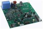


 工商网监
湘ICP备2023018690号
工商网监
湘ICP备2023018690号

