DS1052
5-Bit, Programmable, 100kHz
Pulse-Width Modulator
www.maxim-ic.com
FEATURES
§
§
§
§
§
§
§
PIN ASSIGNMENT
Single 5-bit, programmable, pulse-width
modulator (PWM)
Adjustable Duty Cycle: 0% to 100%
2.7V to 5.5V Operation
Standard Frequency Value: 100kHz
2-Wire Addressable Interface
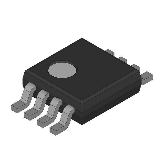
Packages: 8-Pin (150-mil) SOIC and 8-Pin
(118-mil) mSOP
Operating Temperature: -40oC to +85oC
100kHz
100kHz
1
8
VCC
SDA
2
7
A1
A0
3
6
A2
GND
4
5
PWMo
8-Pin 150-mil SOIC
8-Pin 118-mil mSOP
ORDERING INFORMATION
DS1052Z-100
DS1052U-100
SCL
8-Pin 150-mil SOIC
8-Pin 118-mil mSOP
PIN DESCRIPTION
VCC
PWMO
A0, A1, A2
SDA
SCL
GND
- 2.7V to 5.5V Power Supply
- PWM Ouput
- Device Address
- Serial Data I/O
- Serial Clock Input
- Ground
DESCRIPTION
The DS1052 is a programmable, 5-bit, pulse-width modulator featuring a 2-wire addressable controlled
interface. The DS1052 operates from power supplies ranging from 2.7V up to 5.5V. The PWM output
provides a signal that swings from 0V to VCC.
The DS1052-100 requires a typical operating current of 100µA and a programmable shutdown supply
current of 1µA.
One standard PWM output frequency is offered: 100kHz. The 2-wire addressable interface allows
operation of multiple devices on a single 2-wire bus and provides compatibility with other Dallas
Semiconductor 2-wire devices such as real-time clocks (RTCs), digital thermometers, and digital
potentiometers.
The device is ideal for low-cost LCD contrast and/or brightness control, power supply voltage
adjustment, and battery charging or current adjustment. The DS1052 is offered in standard integrated
circuit packaging, including the 8-pin (150-mil) SOIC and space-saving 8-pin (118-mil) mSOP.
1 of 14
072601
�DS1052
OPERATION
Interface protocol is simplified to an 8-bit control byte and 8-bit data byte. Information can be read or
written to the DS1052 including a commanded shutdown operation.
Power-Up Configuration
The DS1052 powers-up to half-scale (10000B) providing 50% duty-cycle. In this mode, the DS1052 can
be used as a standalone oscillator of the frequency specified. Once powered, the PWM output can be
changed via the 2-wire addressable serial port.
Pin Description
Vcc – Power supply terminal. The DS1052 will support operation from power supply voltages ranging
from +2.7 volts to +5.5 volts.
GND – Ground terminal.
PWMO – Pulse-width modulated output. This output is a square-wave having amplitudes from 0 volts to
VCC. The duty cycle of this output is governed by a 5-bit control register. Output duty cycles range from
0% to 96.88%. An additional command sequence will provide a 100% duty cycle or “full-on.”
SCL – Serial clock input.
SDA – Serial bi-directional data I/O.
A0, A1, A2 – Device address (chip selects).
2-Wire Addressable Serial Port Control
The 2-wire serial port interface supports a bi-directional data transmission protocol with device
addressing. A device that sends data on the bus is defined as a transmitter, and a device receiving data as
a receiver. The device that controls the message is called a “master.” The devices that are controlled by
the master are “slaves.” The bus must be controlled by a master device that generates the serial clock
(SCL), controls the bus access, and generates the START and STOP conditions. The DS1052 operates as
a slave on the 2-wire bus. Connections to the bus are made via the open-drain I/O lines SDA and SCL.
The following I/O terminals control the 2-wire serial port: SDA, SCL, A0, A1, and A2. A 2-wire serial
port overview and timing diagrams for the 2-wire serial port can be found in Figures 2 and 5,
respectively. Timing information for the 2-wire serial port is provided in the “AC Electrical
Characteristics” table for 2-wire serial communications.
2 of 14
�DS1052
The following bus protocol has been defined (See Figure 2):
§ Data transfer may be initiated only when the bus is not busy.
§ During data transfer, the data line must remain stable whenever the clock line is HIGH. Changes in
the data line while the clock line is high will be interpreted as control signals.
Accordingly, the following bus conditions have been defined:
Bus not busy: Both data and clock lines remain HIGH.
Start data transfer: A change in the state of the data line from HIGH to LOW while the clock is HIGH,
defines a START condition.
Stop data transfer: A change in the state of the data line from LOW to HIGH while the clock line is
HIGH defines the STOP condition.
Data valid: The state of the data line represents valid data when, after a START condition, the data line
is stable for the duration of the HIGH period of the clock signal. The data on the line must be changed
during the LOW period of the clock signal. There is one clock pulse per bit of data. Figure 2 details how
data transfer is accomplished on the 2-wire bus. Depending upon the state of the R/W bit, two types of
data transfer are possible.
Each data transfer is initiated with a START condition and terminated with a STOP condition. The
number of data bytes transferred between START and STOP conditions is not limited and is determined
by the master device. The information is transferred byte-wise and each receiver acknowledges with a
ninth bit.
Within the bus specifications, a regular mode (100kHz clock rate) and a fast mode (400kHz clock rate)
are defined. The DS1052 works in both modes.
Acknowledge: Each receiving device, when addressed, is obliged to generate an acknowledge after the
reception of each byte. The master device must generate an extra clock pulse that is associated with this
acknowledge bit.
A device that acknowledges must pull down the SDA line during the acknowledge clock pulse in such a
way that the SDA line is stable LOW during the HIGH period of the acknowledge-related clock pulse. Of
course, setup and hold times must be taken into account. A master must signal an end of data to the slave
by not generating an acknowledge bit on the last byte that has been clocked out of the slave. In this case,
the slave must leave the data line HIGH to enable the master to generate the STOP condition.
1. Data transfer from a master transmitter to a slave receiver. The first byte transmitted by the
master is the command/control byte. Next follows a number of data bytes. The slave returns an
“acknowledge” bit after each received byte.
2. Data transfer from a slave transmitter to a master receiver. The first byte (the command/control
byte) is transmitted by the master. The slave then returns an acknowledge bit. Next follows a number
of data bytes transmitted by the slave to the master. The master returns an acknowledge bit after all
received bytes other than the last byte. At the end of the last received byte, a “not acknowledge” is
returned.
3 of 14
�DS1052
The master device generates all serial clock pulses and the START and STOP conditions. A transfer is
ended with a STOP condition or with a repeated START condition. Since a repeated START condition is
also the beginning of the next serial transfer, the bus will not be released.
The DS1052 may operate in the following two modes:
1. Slave receiver mode: Serial data and clock are received through SDA and SCL, respectively. After
each byte is received, an acknowledge bit is transmitted. START and STOP conditions are recognized
as the beginning and end of a serial transfer. Address recognition is performed by hardware after
reception of the slave (device) address and direction bit.
2. Slave transmitter mode: The first byte is received and handled as in the slave receiver mode.
However, in this mode the direction bit will indicate that the transfer direction is reversed. Serial data
is transmitted on SDA by the DS1052 while the serial clock is input on SCL. START and STOP
conditions are recognized as the beginning and end of a serial transfer.
SLAVE ADDRESS
A command/control byte is the first byte received following the START condition from the master
device. The command/control byte consists of a four-bit control code. For the DS1052, this is set as 0101
binary for read/write operations. The next three bits of the command/control byte are the device select
bits or slave address (A2, A1, A0). They are used by the master device to select which of eight possible
devices is to be accessed. When reading or writing the DS1052, the device select bits must match the
device select pins (A2, A1, A0). The last bit of the command/control byte (R/W) defines the operation to
be performed. When set to a one a read operation is selected, and when set to a zero a write operation is
selected. The command control byte is presented in Figure 3.
Following the START condition, the DS1052 monitors the SDA bus checking the device type identifier
being transmitted. Upon receiving the 0101 control code, the appropriate device address bits, and the
read/write bit, the slave device outputs an “acknowledge” signal on the SDA line.
COMMAND AND PROTOCOL
The command and protocol structure of the DS1052 allows the user to read or write the PWM
configuration register or place the device in a low-current state (shut-down mode) and recall the device
from a low-current state. Additionally, the 2-wire command/protocol structure of the DS1052 will support
eight different devices that can be uniquely controlled.
Figure 4a, b, c, d, & e show the five different command and protocol bytes for the DS1052. These include
the following command operations: 1) Set PWM duty cycle, 2) Set PWM duty cycle 100%, 3) Set
shutdown mode, 4) Set recall mode, 5) Read PWM configuration register.
The command operation “Set PWM Duty Cycle” is used to configure the output duty cycle of the device.
The DS1052 has a 5-bit resolution and is capable of setting the duty cycle output from 0% up to 96.88%
in steps of 3.125%. A binary value of (00000B) sets the duty cycle output at 0% while a binary value of
(11111B) sets the duty cycle output at 96.88%.
The command operation “Set PWM Duty Cycle 100%” is used to configure the output duty cycle of the
device to a “full-on.” This command is provided in addition to the Set PWM Duty Cycle command for
flexibility and convenience in total duty cycle coverage. It allows the user to provide a total duty cycle
range from 0% to 100%.
4 of 14
�DS1052
The command operation “Set Shutdown Mode” is used to provide a low-current (inactive state) state for
the DS1052. When in a low-current state the DS1052 will draw currents less than or equal to 1mA. The
PWMO output will be high impedance.
The command operation “Set Recall Mode” is used to recall the DS1052 from a low-current state. The
value of the PWMO output is recalled to that prior to initiating a “Set shutdown mode” command.
The “Read PWM Duty Cycle” command is used to read the current setting of the PWM configuration
register. Information returned by this command includes PWM output value as well as whether the device
is in a shutdown configuration.
PWM data values and control/command values are always transmitted most significant bit (MSB) first.
During communications, the receiving unit always generates the “acknowledge.”
READING THE DS1052
As shown in Figure 4e, the DS1052 provides one read command operation. This operation allows the
user to read the current setting of the PWM configuration register. Specifically, the R/W bit of the
command/control byte is set equal to a 1 for a read operation. Communication to read the DS1052 begins
with a START condition which is issued by the master device. The command/control byte from the
master device will follow the START condition. Once the command/control byte has been received by
the DS1052, the part will respond with an ACKNOWLEDGE. The read/write bit of the command/control
byte, as stated, should be set equal to 1 for reading the DS1052.
When the master has received the ACKNOWLEDGE from the DS1052, the master can then begin to
receive the PWM configuration register data. As mentioned this data will be transmitted MSB first. Once
the eight bits of the PWM configuration register have been transmitted, the master will need to issue an
ACKNOWLEDGE, unless it is the only byte to be read, in which case the master issues a NOT
ACKNOWLEDGE. If desired the master may stop the communication transfer at this point by issuing the
STOP condition. Final communication transfer is terminated by issuing the STOP command. Again, the
flow of the read operation is presented in Figure 4e.
WRITING THE DS1052
A data flow diagram for writing the DS1052 is shown in Figures 4a, b, c, and d. The DS1052 has three
write commands that are used to change the PWM configuration register or the shutdown and recall mode
of the device.
All the write operations begin with a START condition. Following the START condition, the master
device will issue the command/control byte. The read/write bit of the command/control byte will be set to
“0” for writing the DS1052. Once the command/control byte has been issued and the master receives the
acknowledgment from the DS1052, PWM configuration data is transmitted to the DS1052 by the master
device.
A data byte for the DS1052 will contain PWM configuration data and shutdown/recall command data.
The five least significant bits of data specify the PWM configuration value while the three most
significant bits specify the whether the device is to be shutdown or recalled. When the DS1052 has
received the data byte, it will respond with an ACKNOWLEDGE. At this point, the new PWM
configuration register value and shutdown/recall command value will be updated in the DS1052. The
master device, after the receipt of the ACKNOWLEDGE, can continue to transmit additional data bytes
5 of 14
�DS1052
or if the transaction is complete respond with the STOP condition. The 2-wire serial timing diagram is
presented in Figure 5.
6 of 14
�DS1052
ABSOLUTE MAXIMUM RATINGS*
Voltage on Any Pin Relative to Ground
Operating Temperature
Storage Temperature
Soldering Temperature
-0.3V to +6.0V
-40oC to +85oC
-55oC to +125oC
See J-STD-020A specification
* This is a stress rating only and functional operation of the device at these or any other conditions above
those conditions indicated in the operation section of the specification is not implied. Exposure to
absolute maximum rating conditions for extended periods of time may affect reliability.
RECOMMENDED DC OPERATING CONDITIONS
(-40°C to +85°C; VCC = 2.7V to 5.5V)
PARAMETER
Supply voltage
SYMBOL
VCC
MIN
+2.7
DC ELECTRICAL CHARACTERISTICS
PARAMETER
Active Supply
Current
Input Leakage
Input Logic 1
Input Logic 0
Input Current Each
I/O Pin
Standby Current
SYMBOL
ICC
LOW Level Ouput
Voltage (SDA)
VOL1
ILI
VIH
VIL
0.4


 工商网监
湘ICP备2023018690号
工商网监
湘ICP备2023018690号
