DS1239
MicroManager Chip
www.dalsemi.com
FEATURES
�
�
�
�
�
�
�
�
�
�
�
�
�
�
�
Provides necessary control for start up and
shutdown of power supply from keyboard
Holds microprocessor in check during power
transients
Halts and restarts an out-of-control
microprocessor
Monitors push button for external override
Warns microprocessor of an impending power
failure
Converts CMOS SRAM into nonvolatile
memory
Unconditionally write-protects memory when
power supply is out of tolerance
Consumes less than 100 nA of battery current
Controls external power switch for high
current applications
Accurate 10% power supply monitoring
Optional 5% power supply monitoring
designated DS1239-5
Provides orderly shutdown in nonvolatile
microprocessor applications
Supplies necessary control for low-power
“stop mode” in battery operate hand-held
applications
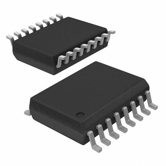
Standard 16-pin DIP or space-saving 16-pin
SOIC
Optional industrial temperature range -40°C
to +85°C
PIN ASSIGNMENT
VBAT
1
16
PSO
VCCO
2
15
RST
VCC
3
14
PBRST
GND
4
13
CEI
PF
5
12
PF
6
11
WC/SC
7
10
PSI
8
9
VBAT
VCCO
CEO
VCC
GND
ST
PF
NMI
PF
WC/SC
IN
PSI
DS1239 16-Pin DIP (300-mil)
See Mech. Drawings Section
1
2
3
4
5
6
7
8
16
15
14
13
12
11
10
9
PSO
RST
PBRST
CEI
CEO
ST
NMI
IN
DS1239 16-Pin SOIC (300-mil)
See Mech. Drawings Section
PIN DESCRIPTION
VBAT
VCCO
VCC
GND
PF
PF
WC/ SC
PSI
IN
NMI
ST
CEO
CEI
PBRST
RST
PSO
- +3 Volt Battery Input
- Switched SRAM Supply Output
- +5 Volt Power Supply Input
- Ground
- Power Fail (Active High)
- Power Fail (Active Low)
- Wake-Up Control (Sleep)
- Power Supply Control Input
- Early Warning Input
- Non-Maskable Interrupt
- Strobe Input
- Chip Enable Output
- Chip Enable Input
- Pushbutton Reset Input
- Reset Output (Active low)
- Power Supply Control Outputs
DESCRIPTION
The DS1239 MicroManager provides all the necessary functions for power supply control and
monitoring, reset control, and memory backup in microprocessor-based systems. Using the DS1239, an
AC power switch is no longer required for microprocessor-based systems. A keyboard control system for
power supply start up and shutdown is provided through the use of the Power Supply Control Input and
Output. In other respects, the DS1239 is functionally identical to a DS1236 in the NMOS mode. For a
complete description of the other DS1239 features, refer to the DS1236 data sheet. Pin-out of the
1 of 4
111899
�DS1239
DS1239 is identical to the DS1236 with two exceptions. The RC and RST pins have been replaced with
PSI and PSO, respectively. Other pins and functions operate exactly as the DS1236 in NMOS mode.
POWER SUPPLY CONTROL
The DS1239 facilitates the power-up and power-down sequencing of a main power supply from a
keyboard or pushbutton. The Power Supply Control Input ( PSI ) and Power Supply Control Output (PSO)
are used for this purpose. Prior to establishing a voltage on VCC (+5V), the PSI is internally held at a high
level at all times with the VBAT supply. When PSI is forced low via a keypad or other source, the PSO is
connected to the VBAT to provide a high level. As shown in Figure 1, this active high signal can be wired
directly to an optically isolated SCR to initiate an AC to DC power-up sequence. This in turn will provide
the supply voltage for VCC. The timing is illustrated in Figure 2. Holding the PSI input low, the PSO
output will supply a connection to the VBAT pin until the VCC reaches VBAT, or a maximum of 500 ms. If
the supply voltage on VCC rises above the VBAT level before the tPSI timeout, the PSO pin will remain high
and track the VCC input. If VCC does not rise above VBAT before either tPSI or PSI is allowed to return to a
high level, the PSO output will return to tristate. Once the PSO output and VCC are set at a high level, a
subsequent falling edge on PSI will tristate PSO to initiate a shut down condition. The 10 microamp
current supplied by the PSI pin allows the use of a 0.1 µF capacitor as a simple pushbutton debounce
circuit. The battery size for this application must be selected to provide the SCR on-current for the power
supply response time and is consequently application-specific.
POWER SUPPLY CONTROL Figure 1
2 of 4
�DS1239
POWER SUPPLY CONTROL TIMING Figure 2
ABSOLUTE MAXIMUM RATINGS*
Voltage on VCC Pin Relative to Ground
Voltage on I/O Relative to Ground
Operating Temperature
Operating Temperature (Industrial Version)
Storage Temperature
Soldering Temperature
*
-0.5V to +7.0V
-0.5V to VCC + 0.5V
0°C to 70°C
-40°C to +85°C
-55°C to +125°C
260°C for 10 seconds
This is a stress rating only and functional operation of the device at these or any other conditions
above those indicated in the operation sections of this specification is not implied. Exposure to
absolute maximum rating conditions for extended periods of time may affect reliability.
These specifications reflect the power supply control feature of the DS1239. For complete electrical
specifications, refer to the DS1236 data sheet.
3 of 4
�DS1239
DC ELECTRICAL CHARACTERISTICS
PARAMETER
PSI
Output Current
(0°C to 70°C; VCC= 4.5V to 5.5V)
SYMBOL
IPSI
MIN
IPSO
10
PSO Output Current
AC ELECTRICAL CHARACTERISTICS
PARAMETER
SYMBOL
TYP
3
MAX
UNITS
µA
NOTES
mA
3
(0°C to 70°C; VCC= 4.5V to 5.5V)
MIN
TYP
MAX
UNITS
NOTES
1
PSI
to Valid VCC
tPSI
200
ms
PSI
to PSO Tri-state
tPST
20
ns
PSI
to Valid PSO
tPSO
100
ns
PSO Pulse Width
tPSP
500
ms
200
NOTES:
1. Minimum turn-on response time for AC-to-DC power supply.
2. PSO pulse width for VCC held below VBAT.
3. PSO will typically source 1.5 mA at 1.5V with VCC= 0V, VBAT= 3V.
4 of 4
2
�
很抱歉,暂时无法提供与“DS1239S-10+”相匹配的价格&库存,您可以联系我们找货
免费人工找货