DS1961S
1kb Protected EEPROM iButton
With SHA-1 Engine
www.maxim-ic.com
SPECIAL FEATURES
§
§
§
§
§
§
§
§
§
§
1128 Bits of 5V EEPROM Memory
Partitioned into Four Pages of 256 Bits, a 64Bit Write-Only Secret, and up to Five
General-Purpose Read/Write Registers
Write Access Requires Knowledge of the
Secret and the Capability of Computing and
Transmitting a 160-Bit MAC (Message
Authentication Code) as Authorization
Secret and Data Memory can be WriteProtected (All or Page 0 Only) or put in
EPROM-Emulation Mode (“Write to 0”, Page
1)
On-Chip, 512-Bit SHA-1 Engine to Compute
160-Bit MACs and Generate Secrets
Reads and Writes Over a Wide 2.8V to 5.25V
Voltage Range from -40°C to +85°C
Communicates to Host with a Single Digital
Signal at 14.1kbps using 1-Wire® Protocol
On-Chip, 16-Bit Cyclic Redundancy Check
(CRC) Generator for Safeguarding Data
Transfers
Overdrive Mode Boosts Communication
Speed to 125kbps
Operating Temperature Range from -40°C to
+85°C
Minimum 10 Years of Data Retention at
+85°C
§
§
§
§
§
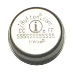
F5 MicroCan
5.89
0.36
§
§
§
§
Unique, Factory-Lasered and Tested 64-Bit
Registration Number (8-Bit Family Code +
48-Bit Serial Number + 8-Bit CRC Tester)
Assures Absolute Traceability Because No
Two Parts are Alike
Multidrop Controller for 1-Wire Net
Digital Identification and Information by
Momentary Contact
Chip-Based Data Carrier Compactly Stores
Information
Data can be Accessed While Affixed to
Object
iButton, 1-Wire, and MicroCan are registered trademarks of
Dallas Semiconductor.
0.51
© 1993
YYWW REGISTERED
16.25
RR
33
xx
17.35
000000FBD8B3
IO
GND
F3 MicroCan
3.10
COMMON iButton FEATURES
§
Button Shape is Self-Aligning with CupShaped Probes
Durable Stainless-Steel Case Engraved with
Registration Number Withstands Harsh
Environments
Easily Affixed with Self-Stick Adhesive
Backing, Latched by its Flange, or Locked
with a Ring Pressed onto its Rim
Presence Detector Acknowledges when
Reader First Applies Voltage
Meets UL#913 (4th Edit.). Intrinsically Safe
Apparatus: Approved Under Entity Concept
for use in Class I, Division 1, Groups A, B, C,
and D Locations (Application Pending)
0.36
0.51
© 1993
YYWW REGISTERED
xx
16.25
RR
33
17.35
000000FBC52B
IO
GND
All dimensions are shown in millimeters.
1 of 36
092302
�DS1961S
ORDERING INFORMATION
EXAMPLES OF ACCESSORIES
DS1961S-F5
DS1961S-F3
DS1963S
DS9096P
DS9101
DS9093RA
DS9093A
DS9092
F5 iButton
F3 iButton
SHA Coprocessor and Button
Self-Stick Adhesive Pad
Multipurpose Clip
Mounting Lock Ring
Snap-In Fob
iButton Probe
iButton DESCRIPTION
The DS1961S combines 1024 bits of EEPROM, a 64-bit secret, an 8-byte register/control page with up to
five user-read/write bytes, a 512-bit SHA-1 engine, and a fully featured 1-Wire interface in a rugged
iButton. Data is transferred serially through the 1-Wire protocol, which requires only a single data lead
and a ground return. The DS1961S has an additional memory area called the scratchpad that acts as a
buffer when writing to the main memory, the register page, or when installing a new secret. Data is first
written to the scratchpad from where it can be read back. After the data has been verified, a copy
scratchpad command transfers the data to its final memory location, provided that the DS1961S receives
a matching 160-bit MAC. The computation of the MAC involves the secret and additional data stored in
the DS1961S including the device’s identity register. Only a new secret can be loaded without providing
a MAC. The SHA-1 engine can also be activated to compute 160-bit MACs when reading a memory page
or to compute a new secret, instead of loading it.
The DS1961S understands a unique command "Refresh Scratchpad." Proper use of a refresh sequence
after a copy scratchpad operation reduces the number of weak bit failures in a touch environment (see the
Writing with Verification section). The refresh sequence also provides a means to restore functionality in
a device with bits in a weak state.
Each DS1961S has its own 64-bit ROM registration number that is factory lasered into the chip to
provide a guaranteed unique identity for absolute traceability. The durable stainless-steel package is
highly resistant to environmental hazards such as dirt, moisture, and shock. Its compact coin-shaped
profile is self-aligning with mating receptacles, allowing the DS1961S to be easily used by human
operators. Accessories permit the DS1961S to be mounted on almost any surface including plastic key
fobs and photo-ID badges.
APPLICATIONS
The DS1961S can be used for different purposes such as secure access control, user/product authentication, after-market management of consumables, and as monetary tokens in electronic payment systems.
As carrier of electronic cash (eCash), the DS1961S can store up to three monetary files or "purses" of a
single service provider, which make the device well suited for company-sized single-secret applications
such as cafeteria, copy machines, and access control at entertainment parks or private clubs. For increased
security or if the processing power of the host microcontroller is insufficient, a DS1963S can be used as
secure coprocessor to verify MACs generated by the DS1961S or to compute MACs needed for writing
to the DS1961S.
OVERVIEW
The block diagram in Figure 1 shows the relationships between the major control and memory sections of
the DS1961S. The DS1961S has five main data components: 1) 64-bit lasered ROM, 2) 64-bit scratchpad,
3) four 32-byte pages of EEPROM, 4) 64-bit register page, 5) 64-bit secrets memory, and 6) a 512-bit
2 of 36
�DS1961S
SHA-1 (Secure Hash Algorithm) engine. The hierarchical structure of the 1-Wire protocol is shown in
Figure 2. The bus master must first provide one of the seven ROM function commands, 1) Read ROM, 2)
Match ROM, 3) Search ROM, 4) Skip ROM, 5) Resume Communication, 6) Overdrive-Skip ROM, or 7)
Overdrive-Match ROM. Upon completion of an overdrive ROM command byte executed at standard
speed, the device enters overdrive mode where all subsequent communication occurs at a higher speed.
The protocol required for these ROM function commands is described in Figure 9. After a ROM function
command is successfully executed, the memory functions become accessible and the master can provide
any one of the eight memory and SHA function commands. The protocol for these memory and SHA
function commands is described in Figure 7. All data is read and written LSB first.
Figure 1. DS1961S BLOCK DIAGRAM
Parasite Power
1-Wire Net
1-Wire
Function Control
Memory and
SHA Function
Control Unit
64-bit
Lasered ROM
512-bit
Secure Hash
Algorithm
Engine
CRC16
Generator
64-bit
Scratchpad
Data Memory
4 Pages of
256 bits Each
Register Page
64-bit
Secrets Memory
64-bit
64-BIT LASERED ROM
Each DS1961S contains a unique ROM code that is 64 bits long. The first eight bits are a 1-Wire family
code. The next 48 bits are a unique serial number. The last eight bits are a CRC of the first 56 bits (see
Figure 3). The 1-Wire CRC is generated using a polynomial generator consisting of a shift register and
XOR gates as shown in Figure 4. The polynomial is X8 + X5 + X4 + 1. Additional information about the
Dallas 1-Wire CRC is available in The Book of DS19xx iButton Standards from Dallas Semiconductor.
The shift register bits are initialized to zero. Then starting with the LSB of the family code, one bit at a
time is shifted in. After the 8th bit of the family code has been entered, then the serial number is entered.
After the 48th bit of the serial number has been entered, the shift register contains the CRC value.
Shifting in the eight bits of CRC should return the shift register to all zeros.
3 of 36
�DS1961S
Figure 2. HIERARCHICAL STRUCTURE FOR 1-WIRE PROTOCOL
1-Wire Net
Bus
Master
Other
Devices
DS1961S
Command
Level:
1-Wire ROM Function
Commands (See Figure 9)
DS1961S-Specific
Memory Function
Commands (See Figure 7)
Available
Commands:
Data Field
Affected:
Read ROM
Match ROM
Search ROM
Skip ROM
Resume
Overdrive Skip
Overdrive Match
64-bit Reg. #, RC-Flag
64-bit Reg. #, RC-Flag
64-bit Reg. #, RC-Flag
RC-Flag
RC-Flag
64-bit Reg. #, RC-Flag, OD-Flag
64-bit Reg. #, RC-Flag, OD-Flag
Write Scratchpad
Read Scratchpad
Load First Secret
64-bit Scratchpad, Flags
64-bit Scratchpad
Secret, Flags; Data Memory (after
Refresh Scratchpad)
Secret, Data Memory, Scratchpad
Data Memory or Register Page,
Secret, Flags, 64-Bit Reg. #,
Data Memory, Secret, 64-bit Reg. #,
3-Byte Challenge in Scratchpad
Data Memory, Register Page, Reg. #
64-bit Scratchpad, Data Memory,
Flags
Compute Next Secret
Copy Scratchpad
Read Authenticated Page
Read Memory
Refresh Scratchpad
Figure 3. 64-BIT LASERED ROM
MSB
LSB
8-Bit CRC Code
MSB
48-Bit Serial Number
LSB
MSB
8-Bit Family Code (33h)
LSB
4 of 36
MSB
LSB
�DS1961S
Figure 4. 1-WIRE CRC GENERATOR
8
5
4
Polynomial = X + X + X + 1
1st
STAGE
X
0
2nd
STAGE
X
1
3rd
STAGE
X
2
4th
STAGE
X
3
5th
STAGE
X
4
6th
STAGE
X
5
7th
STAGE
X
6
8th
STAGE
X
7
X
8
INPUT DATA
MEMORY MAP
The DS1961S has four memory areas: data memory, secrets memory, register page with special function
registers and user-bytes, and a scratchpad. The data memory is organized in pages of 32 bytes. Secret,
register page, and scratchpad are 8 bytes each. The scratchpad acts as a buffer when writing to the data
memory, loading the initial secret or when writing to the register page.
Data memory, secrets memory, and the register page are located in a linear address space, as shown in
Figure 5. The data memory and the register page have unrestricted read access. Writing to the data
memory and the register page requires knowledge of the secret.
Figure 5. DS1961S MEMORY MAP
ADDRESS RANGE
DESCRIPTION
NOTE
0000h to 001Fh
Data Memory Page 0
No Write-Access Without Secret
0020h to 003Fh
Data Memory Page 1
No Write-Access Without Secret
0040h to 005Fh
Data Memory Page 2
No Write-Access Without Secret
0060h to 007Fh
Data Memory Page 3
No Write-Access Without Secret
0080h to 0087h
Secrets Memory
No Read Access; No Secret Needed for
Write Access
0088h
1)
Write-Protect Secret, 008Ch to 008Fh
Protection Activated by Code AAh or 55h
0089h
1)
Write-Protect Pages 0 to 3
Protection Activated by Code AAh or 55h
008Ah
1)
User Byte, Self-Protecting
Protection Activated by Code AAh or 55h
Factory Byte (Read Only)
Reads Either AAh or 55h; See Text
User Byte/EPROM Mode Control for
Page 1
Mode Activated by Code AAh or 55h
User Byte/Write-Protect Page 0 Only
Protection Activated by Code AAh or 55h
008Eh to 008Fh
User Bytes/Manufacturer ID
Function Depends on Factory Byte
0090h to 0097h
64-Bit Identity Register
Read-Only Access
008Bh
008Ch
1)
008Dh
1)
1)
Once programmed to AAh or 55h this address becomes read-only. All other codes can be stored but
will neither write-protect the address nor activate any function.
5 of 36
�DS1961S
The secret can be installed either by copying data from the scratchpad to the secrets memory or by
computation using the current secret and the scratchpad contents as partial secret. The secret cannot be
read directly; only the SHA engine has access to it for computing message authentication codes.
The address range 0088h to 008Fh, also referred to as the Register Page, contains special function
registers as well as general-purpose user-bytes and one factory byte. Once programmed to AAh or 55h,
most of these bytes become write-protected and can no longer be altered. All other codes neither writeprotect the address nor activate the special function associated to that particular byte. Special functions
are: 1) write-protecting only the secret, 2) write-protecting all four data memory pages simultaneously, 3)
activating EPROM mode for data memory page 1 only, and 4) write-protecting data memory page 0 only.
Once EPROM mode is activated, bits in the address range 0020h through 003Fh can only be altered from
a logic 1 to a logic 0, provided that the data memory is not write protected.
The factory byte either reads 55H or AAh. Typically, this address reads 55h, indicating that the addresses
008E and 008F are read/write user-bytes without any special function or locking mechanism. The code of
AAh indicates that these two bytes are programmed with a 16-bit manufacturer ID and then writeprotected at the factory. The manufacturer ID can be a customer-supplied identification code that assists
the application software in identifying the product the DS1961S is associated with and in faster selection
of the applicable secret. To setup and register a manufacturer ID contact the factory.
The address range 0090h to 0097h is called the identity register. Typically, the identity register contains a
copy of the device’s ROM registration number. The family code is stored at the lower address followed
by the 48-bit serial number and the 8-bit CRC, which is stored at address 0097h. In reading through these
addresses (0090h to 0097h) the bus master receives the individual bits of the registration number in
exactly the same sequence as with a ROM function command. With customized versions, the content of
the identity register can be any customer-specified constant pattern. For more information on
customization contact the factory.
Figure 6. ADDRESS REGISTERS
Bit Number
7
6
5
4
3
2
1
0
Target Address (TA1)
T7
T6
T5
T4
T3
T2
(0)
T1
(0)
T0
(0)
Target Address (TA2)
T15
T14
T13
T12
T11
T10
T9
T8
Ending Address with
Data Status (E/S)
(Read Only)
AA
1
PF
1
1
E2
(1)
E1
(1)
E0
(1)
ADDRESS REGISTERS AND TRANSFER STATUS
The DS1961S employs three address registers: TA1, TA2, and E/S (Figure 6). These registers are
common to many other 1-Wire devices but operate slightly differently with the DS1961S. Registers TA1
and TA2 must be loaded with the target address to which the data is written or from which data is read.
Register E/S is a read-only transfer-status register, used to verify data integrity with write commands.
Since the scratchpad of the DS1961S is designed to accept data in blocks of eight bytes only, the lower
three bits of TA1 are forced to 0 and the lower three bits of the E/S register (ending offset) always read 1.
6 of 36
�DS1961S
This indicates that all the data in the scratchpad is used for a subsequent copying into main memory or
secret. Bit 5 of the E/S register, called PF or partial byte flag, is a logic-1 if the number of data bits sent
by the master is not an integer multiple of eight or if the data in the scratchpad is not valid due to a loss of
power. A valid write to the scratchpad clears the PF bit. Bits 3, 4, and 6 have no function; they always
read 1. The partial flag supports the master checking the data integrity after a write command. The
highest valued bit of the E/S register is called the AA or authorization accepted flag, which indicates that
the data stored in the scratchpad has already been copied to the target memory address. Writing data to
the scratchpad clears this flag.
WRITING WITH VERIFICATION
To write data to the DS1961S, the scratchpad has to be used as intermediate storage. First the master
issues the write scratchpad command, which specifies the desired target address and the data to be written
to the scratchpad. Note that writes to data memory must be performed on 8-byte boundaries with the three
LSBs of the target address T2–T0 equal to 000b. Therefore, if T2–T0 are sent with non-zero values, the
device sets these bits to zero and uses the modified address as the target address. The master should
always send eight complete data bytes. After the eight bytes of data have been transmitted, the master can
elect to receive an inverted CRC16 of the write scratchpad command, the address as sent by the master,
and the data as sent by the master. The master can compare the CRC to the value it has calculated itself in
order to determine if the communication was successful. After the scratchpad has been written, the master
should always perform a read scratchpad to verify that the intended data was in fact written. During a
read scratchpad, the DS1961S repeats the target address TA1 and TA2 and sends the contents of the E/S
register. The partial flag (bit 5 of the E/S register) is set to 1 if the last data byte the DS1961S received
during a write scratchpad or refresh scratchpad command was incomplete, or if there was a loss of power
since data was last written to the scratchpad. The authorization-accepted (AA) flag (bit 7 of the E/S
register) is normally cleared by a write scratchpad or refresh scratchpad; therefore, if it is set to 1, it
indicates that the DS1961S did not understand the proceeding write (or refresh) scratchpad command. In
either of these cases, the master should rewrite the scratchpad. After the master receives the E/S register,
the scratchpad data is received. The descriptions of write scratchpad and refresh scratchpad provide
clarification of what changes can occur to the scratchpad data under certain conditions. An inverted CRC
of the read scratchpad command, target address, E/S register, and scratchpad data follows the scratchpad
data. As with the write scratchpad command, this CRC can be compared to the value the master has
calculated itself in order to determine if the communication was successful. After the master has verified
the data, it can send the copy scratchpad to copy the scratchpad to memory. Alternatively, the load first
secret or compute next secret command can be issued to change the secret. See the descriptions of these
commands for more information.
In a touch environment the quality of the electrical contact cannot be guaranteed. With poor or
intermittent contact it is possible for a copy scratchpad command to complete with insufficient energy,
leaving the floating gate voltage of an EEPROM bit in the area of the threshold between 0 and 1. When
this occurs, the logical value of the bit is not assured. Depending on voltage and/or temperature
conditions, the same bit can be read by the host as one polarity and then by the internal SHA-1 engine as
the opposite polarity. This becomes a fatal lockup mode because the host cannot formulate a proper SHA1 MAC to enable the bit to be rewritten. To repair poorly written bits and thereby restore the device to
functionality, the refresh scratchpad command was introduced. Combined with the load first secret
command, refresh scratchpad provides a means to restore the EEPROM bits to normal values, removing
lockup conditions and allowing the device to be written again.
To prevent the occurrence of poorly written bits, a refresh sequence should be performed after each copy
scratchpad command. A refresh sequence is defined as a refresh scratchpad (to the same target address as
the previous copy scratchpad), followed by a load first secret. The EN_LFS flag is set by the refresh
7 of 36
�DS1961S
scratchpad command. The EN_LFS flag enables the use of load first secret to addresses 0000h–007Fh.
Using load first secret allows the master to copy the scratchpad to memory without the MAC computation
necessary during a copy scratchpad. If the master attempts any command after refresh scratchpad that
could change the scratchpad data or the target address, EN_LFS is reset to 0. This prevents the use of load
first secret to load any data other than the refreshed memory data to any location other than the one
specified during refresh scratchpad. Refresh scratchpad behaves exactly as write scratchpad does for
target addresses 0080h and above. In this case the EN_LFS flag is not set, so it is not possible to refresh
the data in the secret (0080h) or in the register page (0088h). This prevents the secret from being revealed
by a refresh scratchpad followed by a read scratchpad.
MEMORY AND SHA FUNCTION COMMANDS
Due to its design as a secure device, the DS1961S has to behave differently from other memory iButtons.
Although most of the memory of the DS1961S can be read the same way as any other memory iButton,
attempts to read the secret results in FFh-bytes rather than real data. The Memory and SHA Function
Flow Chart (Figure 7) describes the protocols necessary for accessing the memory and operating the SHA
engine. The communication between master and DS1961S takes place either at regular speed (default,
OD = 0) or at overdrive speed (OD = 1). If not explicitly set into overdrive mode the DS1961S assumes
regular speed.
Write Scratchpad [0Fh]
The write scratchpad command applies to the data memory, the secret and the writeable addresses in the
register page. If the bus master sends a target address higher than 90h, the command is not executed.
After issuing the write scratchpad command, the master must first provide the 2-byte target address,
followed by the data to be written to the scratchpad. The data is written to the scratchpad starting at the
beginning of the scratchpad. Note that the ending offset (E2..E0, see Figure 6) is always 111b regardless
of the number of bytes that the master has transmitted. For this reason the master should always send
eight bytes, especially if the data is to be loaded as a secret. If the master sends less than eight data bytes
and does not read back the scratchpad for verification, parts of the new secret can be random data that is
unknown to the master. Only full data bytes are accepted. If the last data byte is incomplete its content is
ignored and the partial byte flag (PF) is set.
When executing the write scratchpad command the CRC generator inside the DS1961S (see Figure 12)
calculates a CRC of the entire data stream, starting at the command code and ending at the last data byte
as sent by the master. This CRC is generated using the CRC16 polynomial by first clearing the CRC
generator and then shifting in the command code (0Fh) of the write scratchpad command, the target
addresses (TA1 and TA2), and all the data bytes. Note that the CRC16 calculation is performed with the
actual TA1 sent by the master even though the DS1961S sets TA1 bits T2..T0 to 000b for the actual write
scratchpad command. The master can end the write scratchpad command at any time. However, if the
scratchpad is filled to its capacity, the master can send 16 read-time slots and receives the CRC generated
by the DS1961S. If the master continues reading after the CRC all data is be FFh.
After receiving the target addresses (TA1 and TA2), the DS1961S clears the EN_LFS flag. If EPROM
mode is active and a write scratchpad is attempted within page 1 (0020h–003Fh), the scratchpad is loaded
with the logical AND of the scratchpad data sent by the master and the current content of the target
memory location. If a write scratchpad is attempted to the register page (0088h–008Fh), any bytes that
are write-protected overwrite the corresponding scratchpad data byte sent by the master with the existing
value. In all other cases, the data sent by the master is written to the scratchpad unaltered.
8 of 36
�DS1961S
Read Scratchpad [AAh]
The read scratchpad command allows verifying the target address and the integrity of the scratchpad data.
After issuing the command code, the master begins reading. The first two bytes is the target address with
T2 to T0 = 0. The next byte is the ending offset/data status byte (E/S) followed by the scratchpad data,
which may be different from what the master has originally sent. This is of particular importance if the
target address is the secret, the register page, page 1 (in EPROM mode), or if refresh was used to load the
scratchpad. In these cases, the scratchpad can contain data other than that which was sent during either
the write scratchpad or refresh scratchpad commands. The master should read through the end of the
scratchpad after which it receives the inverted CRC that is computed with the data as sent by the
DS1961S. If the master continues reading after the CRC all data is FFh.
The scratchpad can be loaded using the write scratchpad or refresh scratchpad command. The data found
in the scratchpad depends on the command used, the target address, and whether or not EPROM mode is
active. See the descriptions of write scratchpad and refresh scratchpad for clarification.
Load First Secret [5Ah]
The load first secret command has two modes of operation, which are controlled by the EN_LFS flag.
With EN_LFS = 0, the command replaces the device’s current secret with the contents of the scratchpad,
provided that the secret is not write-protected. With EN_LFS = 1, the command allows to rewrite
memory data (addresses 0000h to 007Fh), bypassing the SHA-1 computation that is required when doing
the same through the copy scratchpad command. The EN_LFS flag is 0 unless it has been set to 1 by
executing the refresh scratchpad command prior to load first secret.
Case EN_LFS = 0
Before the load first secret command can be used in this mode, the master must have written the new
secret to the scratchpad using the starting address of the secret (0080h). After issuing the load first secret
command, the master must provide a 3-byte authorization pattern (TA1, TA2, E/S, in that order), that
should have been obtained by an immediately preceding read scratchpad command. This 3-byte pattern
must exactly match the data contained in the three address registers (see Figure 6). If the pattern matches
and the secret is not write-protected, the AA flag is set and the copy begins. All eight bytes of scratchpad
contents are copied to the secret’s memory location.
Case EN_LFS = 1
To use the load first secret command in this mode, the refresh scratchpad command must have been
executed to load eight bytes of memory data (address range 0000h to 007Fh) into the scratchpad, which
sets the EN_LFS flag to 1. After issuing the load first secret command, the master must provide a 3-byte
authorization pattern (TA1, TA2, E/S, in that order), that can be obtained by an immediately preceding
read scratchpad command without affecting the EN_LFS flag. This 3-byte pattern must exactly match the
data contained in the three address registers (see Figure 6). If the pattern matches and the memory is not
write-protected, the AA flag is set and the copy begins. All eight bytes of scratchpad contents are copied
to the memory location.
Regardless of the mode used, the duration of the copy operation is tPROG during which the voltage on the
1-Wire bus must not fall below 2.8V. The master should read at least one byte at the conclusion of the
copy delay. Reading AAh indicates that the copy was successful, while reading FFh indicates that the
copy was not successful. Instead of using load first secret with EN_LFS = 0, a new secret can
alternatively be loaded with the copy scratchpad command. However, this approach requires the
knowledge of the current secret and the computation of a 160-bit MAC.
9 of 36
�DS1961S
Figure 7-1. MEMORY AND SHA FUNCTIONS FLOW CHART
From ROM Functions
Flow Chart (Figure 9)
Bus Master TX Memory
Function Command
0Fh
Write Scratchpad ?
To Figure 7
2nd Part
N
Y
Bus Master TX
TA1 (T7:T0), TA2 (T15:T8)
DS1961S Sets EN_LFS = 0
N
Y
Address
< 90h ?
DS1961S Sets Scratchpad
Byte Counter = 0,
Clears PF, AA,
Sets T2:T0 = 0, 0, 0,
Sets E2:E0 = 1, 1, 1
Bus Master
RX “1”s
Master
TX Reset ?
Note:
See the Write
Scratchpad
Description for
Additional
Information.
Master TX Data Byte
To Scratchpad
N
DS1961S
Increments
Byte Counter
Master
TX Reset ?
Y
Partial
Byte ?
N
Y
N
Byte Counter
=7?
Y
N
Y
PF = 1
DS1961S TX CRC16
of Command, Address,
Data Bytes as They
Were Sent by the Bus
Bus Master
RX “1”s
N
Master
TX Reset ?
Y
To ROM Functions
Flow Chart (Figure 9)
10 of 36
From Figure 7
2nd Part
�DS1961S
Figure 7-2. MEMORY AND SHA FUNCTIONS FLOW CHART (continued)
From Figure 7
1st Part
AAh
Read ScratchPad ?
N
To Figure 7
3rd Part
Y
Bus Master RX
TA1 (T7:T0), TA2 (T15:T8)
and E/S Byte
DS1961S Sets Scratchpad
Byte Counter = 0
Bus Master RX
Data Byte from Scratchpad
DS1961S
Increments
Byte Counter
Master
TX Reset ?
Note:
See the Read
Scratchpad
Description for
Additional
Information.
Y
N
N
Byte Counter
=7?
Y
Bus Master RX CRC16
of Command, Address,
E/S Byte, Data Bytes as
Sent by the DS1961S
Bus Master
RX “1”s
N
Master
TX Reset ?
Y
To Figure 7
1st Part
From Figure 7
3rd Part
11 of 36
�DS1961S
Figure 7-3. MEMORY AND SHA FUNCTIONS FLOW CHART (continued)
From Figure 7
2nd Part
5Ah
Load First
Secret ?
To Figure 7
4th Part
N
Y
Bus Master TX
TA1 (T7:T0), TA2 (T15:T8)
and E/S Byte
Note: The 8-Byte Secret Must
First be Written to the
Scratchpad.
Y
Auth. Code
Match ?
N
Address of
Secret ?
N
N
Address