DS2720
Efficient, Addressable Single-Cell
Rechargeable Lithium Protection IC
www.maxim-ic.com
FEATURES
§
§
§
§
§
§
§
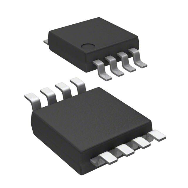
PIN CONFIGURATION
Rechargeable Lithium-Ion (Li+) Safety
Circuit
- Overvoltage Protection
- Overcurrent/Short-Circuit Protection
- Undervoltage Protection
- Overtemperature Protection
Controls High-Side N-Channel Power
MOSFETs Driven from 9V Charge Pump
System Power Management and Control
Feature Support
Eight Bytes of Lockable EEPROM
Dallas 1-Wire® Interface with Unique 64-Bit
Device Address
8-Pin mSOP Package
Low Power Consumption:
- Active Current: 12.5mA typ
- Sleep Current:
1.5mA typ
PLS
1
8
CP
PS
2
7
DC
DQ
3
6
CC
VSS
4
5
VDD
DS2720U
mSOP
PIN DESCRIPTION
PLS PS DQ VSS VDD CP CC DC -
Battery-Pack Positive Terminal Input
Power-Switch Sense Input
Data Input/Output
Device Ground
Power-Supply Input
Reservoir Capacitor
Charge Control Output
Discharge Control Output
DESCRIPTION
The DS2720 single-cell rechargeable Li+ protection IC provides electronic safety functions required for
rechargeable Li+ applications including protecting the battery during charge, protection of the circuit
from damage during periods of excess current flow and maximization of battery life by limiting the level
of cell depletion. Protection is facilitated by electronically disconnecting the charge and discharge
conduction path with switching devices such as low-cost N-channel power MOSFETs.
Since the DS2720 provides high-side drive to external N-channel protection MOSFETs from a 9V charge
pump, superior on-resistance performance results compared to common low-side protector circuits using
the same FETs. The FET on-resistance actually decreases as the battery discharges.
Adding to the uniqueness of the DS2720 is the ability of the system to control the FETs from either the
data interface or a dedicated input thereby eliminating the power-switch control redundancy of
rechargeable Li+ battery systems.
Through its 1-Wire interface, the DS2720 gives the host system read/write access to status and control
registers, instrumentation registers, and general-purpose data storage. Each device has a factoryprogrammed 64-bit net address that allows it to be individually addressed by the host system.
1-Wire is a registered trademark of Dallas Semiconductor.
1 of 21
080205
�DS2720
Two types of user-memory are provided on the DS2720 for battery information storage: EEPROM and
lockable EEPROM. EEPROM memory saves important battery data in true nonvolatile (NV) memory
that is unaffected by severe battery depletion, accidental shorts, or ESD events. Lockable EEPROM
becomes ROM when locked to provide additional security for unchanging battery data.
ORDERING INFORMATION
PART
DS2720AU+
DS2720AU+T&R
DS2720BU+
DS2720BU+T&R
DS2720CU+
DS2720CU+T&R
DS2720AU
DS2720AU/T&R
DS2720BU
DS2720BU/T&R
DS2720CU
DS2720CU/T&R
DESCRIPTION
DS2720+ in 8-Lead mSOP in Bulk with VOVA = 4.275V
DS2720+ in 8-Lead mSOP in Tape-and-Reel with VOVA = 4.275V
DS2720+ in 8-Lead mSOP in Bulk with VOVB = 4.35V
DS2720+ in 8-Lead mSOP in Tape-and-Reel with VOVB = 4.35V
DS2720+ in 8-Lead mSOP in Bulk with VOVC = 4.30V
DS2720+ in 8-Lead mSOP in Tape-and-Reel with VOVC = 4.30V
DS2720 in 8-Lead mSOP in Bulk with VOVA = 4.275V
DS2720 in 8-Lead mSOP in Tape-and-Reel with VOVA = 4.275V
DS2720 in 8-Lead mSOP in Bulk with VOVB = 4.35V
DS2720 in 8-Lead mSOP in Tape-and-Reel with VOVB = 4.35V
DS2720 in 8-Lead mSOP in Bulk with VOVC = 4.30V
DS2720 in 8-Lead mSOP in Tape-and-Reel with VOVC = 4.30V
+ Denotes lead-free package.
2 of 21
�DS2720
Figure 1. BLOCK DIAGRAM
DQ
1-WIRE INTERFACE
AND CONTROL
64-BIT ROM
LOCKABLE EEPROM
STATUS/CONTROL
PS
TEMP SENSOR
(Tdevice)
+
+
OUTPUT BUFFER
CP
TMAX
VDD
+
VOV
VCE
+
S
DELAY
tOVD
+ +
+
L
O
G
I
C
DELAY
tUVD
+
VOC
S
R
DELAY
tOCD
(2)
+
PLS
Q
DC
+ +
(1)
RTST
CC
R
VUV
VSS
Q
+
VCH
VSC
+ +
DELAY
tSCD
1) Normally open, closed to enable test current, ITST
2) Normally open, closed to enable test current, ITST, and recovery charge
(See Rechargeable Li+ Protection Circuitry section for more information.)
3 of 21
�DS2720
Table 1. DETAILED PIN DESCRIPTION
SYMBOL
DESCRIPTION
PLS
Battery-Pack Positive Terminal Input. The device monitors the state of the battery
pack’s positive terminal through this pin in order to detect events such as the attachment
of a charger or the removal of a short circuit. Connect PLS to the pack positive terminal
through a 100W resistor.
PS
Power-Switch Sense Input. The device wakes up from sleep mode when it senses the
closure of a switch to VSS on this pin. PS has a high-impedance internal pullup.
DQ
VSS
VDD
CP
CC
DC
Data Input/Out. 1-Wire data line. Open-drain output driver. Connect this pin to the
DATA terminal of the battery pack. DQ has an internal 0.5mA pull-down.
Device Ground. Connect directly to the negative terminal of the battery cell.
Power Supply Input. Connect VDD to the positive terminal of the battery cell through a
decoupling network.
Charge Pump Output. The internal charge pump regulates CP to 9V which supplies
the ON state drive to the protection FETs. Connect a 0.1mF reservoir capacitor from CP
to VSS.
Charge Protection Control Output. Controls an external N-channel high-side charge
protection FET.
Discharge Protection Control Output. Controls an external N-channel high-side
discharge protection FET.
Figure 2. APPLICATION EXAMPLE
102
102
PACK+
100
1k
1k
102
DS2720
330
PS
DATA
330
PLS
CP
PS
DC
DQ
CC
VSS
10
VDD
104
PACK-
4 of 21
104
1-CELL Li+
�DS2720
POWER MODES
The DS2720 has two power modes: active and sleep. While in active mode, the DS2720 continuously
performs safety monitoring. In sleep mode, the DS2720 ceases monitoring activities and drives both the
charge and discharge protection FETs to an “off state”. Upon returning to the active mode from the sleep
mode, DS2720 resumes safety monitoring and conditionally turns on the protection FETs.
Table 2. POWER MODE TRANSITION CONDITIONS
Active ® Sleep
VDD < VUV
Sleep ® Active(1)
PS pulled to VSS or
VPLS > VDD + VCH
(1) DS2720 does not transition to Active Mode if VDD < VSC.
RECHARGEABLE Li+ PROTECTION CIRCUITRY
During active mode, the DS2720 constantly monitors cell voltage and voltage drop across the FETs to
protect the battery from overcharge (overvoltage), overdischarge (undervoltage), and excessive discharge
currents (overcurrent, short circuit). Conditions and DS2720 responses are described in the sections
below and summarized in Table 3 and Figure 3.
Table 3. PROTECTION CONDITIONS AND DS2720 RESPONSES
CONDITION
NAME
ACTIVATION
THRESHOLD
DELAY
RESPONSE
Overvoltage
VDD > VOV
tOVD(1)
Undervoltage
VSC < VDD < VUV
tUVD
CC = VOLCC
CC = VOLCC
Recovery Charge
VDD < VSC or
(while in active
mode) VDD < VCE
Overcurrent
VDD - VPLS > VOC
tOCD
Short Circuit
VDD < VSC
tSCD
Overtemperature
Tdevice > TMAX
RELEASE
THRESHOLD
VDD < VCE or
VDD - VPLS > VOC
DC = VOLDC
VPLS > VDD + VCH and
VDD > VUV
(charger connected)
RTST enabled(2)
VDD ³ VCE
CC = VOLCC
DC = VOLCC
CC = VOLCC
DC = VOLDC
CC = VOLCC
DC = VOLDC
VPLS > VDD - VOC(3)
VPLS > VDD - VOC(3)
Tdevice < TMAX
All voltages are with respect to VSS.
(1) During transition from sleep to active, tOVD = 0.
(2) Recovery charge current is limited by RTST and forward voltage of blocking diode, which prevents discharging through
RTST when recovery charge enabled.
(3) With test current ITST flowing from VDD to PLS (pullup on PLS).
5 of 21
�DS2720
Overvoltage. If the cell voltage sensed at VDD exceeds overvoltage threshold VOV for a period longer
than overvoltage delay tOVD, the DS2720 shuts off the external charge FET and sets the OV flag in the
protection register. Discharging remains enabled during overvoltage. The charge FET is re-enabled
(unless another protection condition prevents it), when the cell voltage falls below charge enable
threshold VCE, or a discharge causes VDD - VPLS > VOC.
Undervoltage. If the cell voltage sensed at VDD drops below undervoltage threshold VUV for a period
longer than undervoltage delay tUVD, the DS2720 shuts off the charge and discharge FETs, sets the UV
flag in the protection register, and enters sleep mode. The DS2720 turns on both the charge and discharge
FETs after the cell voltage rises above VUV and a charger is present.
Short Circuit. If the cell voltage sensed at VDD drops below depletion threshold VSC for a period of tSCD,
the DS2720 shuts off the charge and discharge FETs and sets the DOC flag in the protection register. The
current path through the charge and discharge FETs is not re-established until the voltage on PLS rises
above VDD - VOC. The DS2720 provides a test current through internal resistor RTST from VDD to PLS to
pull up PLS when VDD rises above VSC. The test current allows the DS2720 to detect the removal of the
offending low-impedance load. Additionally, a recovery charge path through RTST from PLS to VDD is
enabled.
Overcurrent. If the voltage across the protection FETs (VDD - VPLS) is greater than VOC for a period
longer than tOCD, the DS2720 shuts off the external charge and discharge FETs and sets the DOC flag in
the protection register. The current path is not re-established until the voltage on PLS rises above VDD VOC. The DS2720 provides a test current through internal resistor RTST from VDD to PLS to detect the
removal of the offending low-impedance load.
Overtemperature. If the device temperature exceeds TMAX, the DS2720 immediately shuts off the
external discharge and charge FETs. The FETs are not turned back on until the cell temperature drops
below TMAX AND the host resets the OT bit.
6 of 21
�DS2720
Figure 3. Li+ PROTECTION CIRCUITRY EXAMPLE WAVEFORMS
VOV
VCE
VDD
VUV
VSC
VCH
0
-VOC
VPLS - VDD
CHARGE
RECOVERY CHARGED THROUGH
ICELL
0
-IOC
-ISC
DISCHARGE
VOHCP
CC
tUVD
tOVD
tON
DC
tSCD
tUVD
tON
tON
tUVD
tOCD
VOLCC
VOHCP
tUVD
VOLDC
POWER
MODE
ACTIVE
OVERCURRENT OR
SHORT TEST
ACTIVE
SLEEP
INACTIVE
ENABLED
RECOVERY
CHARGE
DISABLED
SHORT-CIRCUIT
EVENT
OVERVOLTAGE
UNDERVOLTAGE
EVENT
EVENT
OVERCURRENT
EVENT
UNDERVOLTAGE
EVENT
SEVERE
DEPLETION
Notes:
IOC = Current that produces a voltage drop across FETs equal to VOC threshold.
ISC = Current drawn from the battery during short-circuit event. (Collapses the cell terminal voltage to VSC.)
Above example assumes FET on-resistance values such that the overcurrent threshold, VOC, is reached before the
short-circuit threshold, VSC.
7 of 21
�DS2720
MEMORY
The DS27xx family of products is organized into a 256-byte linear address space with registers for
instrumentation, status, and control in the lower 32 bytes, with lockable EEPROM memory occupying
portions of the remaining address space. All EEPROM memory is general purpose except address 31h,
which should be written with the default values for the status register.
EEPROM memory is shadowed by RAM to eliminate programming delays between writes and to allow
the data to be verified by the host system before being copied to EEPROM. All reads and writes to/from
EEPROM memory in fact access the shadow RAM. In unlocked EEPROM blocks, the write data
command updates shadow RAM. In locked EEPROM blocks, the write data command is ignored. The
copy data command copies the contents of shadow RAM to EEPROM in an unlocked block of EEPROM
but has no effect on locked blocks. The recall data command copies the contents of a block of EEPROM
to shadow RAM regardless of whether the block is locked or not.
Table 4. MEMORY MAP
ADDRESS (hex)
00
01
02–06
07
08
09–1F
20–23
24–2F
30–33
34–FF
(1)
DESCRIPTION
Protection Register
Status Register
Reserved
EEPROM Register
Special Feature Register
Reserved
EEPROM, Block 0
Reserved
EEPROM, Block 1
(31 = Status Register Initialization)
Reserved
READ/WRITE
R/W
R
—
R
R/W
—
R/W (1)
—
R/W (1)
—
Each EEPROM block is read/write until locked by the LOCK command, after which it is read-only.
PROTECTION REGISTER
The protection register consists of flags that indicate protection circuit status and switches that give
conditional control over the charging and discharging paths. Bits OV, UV, and DOC are set when
corresponding protection conditions occur and remain set until cleared by the host system. The format of
the protection register is shown in Figure 4. The function of each bit is described in detail in the following
paragraphs.
Figure 4. PROTECTION REGISTER FORMAT
Address 00
Bit 7
Bit 6
Bit 5
Bit 4
Bit 3
Bit 2
Bit 1
Bit 0
OV
UV
0
DOC
CC
DC
CE
DE
8 of 21
�DS2720
OV—Overvoltage Flag. When set to 1, this bit indicates the battery pack has experienced an overvoltage
condition. This bit does not clear itself after the overvoltage state is corrected, and thus must be reset by
the host system. A reset of this bit should be issued after the battery voltage falls below VCE in order to
detect future events. The OV bit is a volatile R/W bit, initialized to 0 upon power-on-reset (POR).
UV—Undervoltage Flag. When set to 1, this bit indicates the battery pack has experienced an
undervoltage condition. This bit does not clear itself after the undervoltage state is corrected, and thus
should be reset by the host system in order to detect future events. The UV bit is a volatile R/W bit,
initialized to 1 upon POR.
DOC—Overcurrent Flag. When set to 1, this bit indicates the battery pack has experienced an
overcurrent (or short-circuit) condition. This bit does not clear itself after the over/shortcurrent state is
corrected, and thus should be reset by the host system in order to detect future events. The DOC bit is a
volatile R/W bit, initialized to 1 upon POR.
CC—CC Pin Mirror. This read-only bit mirrors the state of the CC output pin. The CC bit is a 1 when the
CC pin is driven high (VOHCC). The CC bit is a 0 when the CC pin is driven low (VOLCC).
DC—DC Pin Mirror. This read-only bit mirrors the state of the DC output pin. The DC bit is a 1 when
the DC pin is driven high (VOHDC). The DC bit is a 0 when the DC pin is driven low (VOLDC).
CE—Charge Enable. Writing a 0 to this bit disables charging (CC output low, external charge FET off)
regardless of cell or pack conditions. Writing a 1 to this bit enables charging, subject to override by the
presence of any protection conditions. The DS2720 automatically sets this bit to 1 when it transitions
from sleep mode to active mode. The CE bit is a volatile R/W bit, initialized to 1 upon POR.
DE—Discharge Enable. Writing a 0 to this bit disables discharging (DC output low, external discharge
FET off) regardless of cell or pack conditions. Writing a 1 to this bit enables discharging, subject to
override by the presence of any protection conditions. The DS2720 automatically sets this bit to 1 when it
transitions from sleep mode to active mode. The DE bit is a volatile R/W bit, initialized to 1 upon POR.
STATUS REGISTER
The default values for the status register bits are stored in lockable EEPROM in the corresponding bits of
address 31h. A recall data command for EEPROM block 1 recalls the default values into the status
register bits. The format of the status register is shown in Figure 5. The function of each bit is described
in detail in the following paragraphs.
Figure 5. STATUS REGISTER FORMAT
Address 01
Bit 7
Bit 6
Bit 5
Bit 4
Bit 3
Bit 2
Bit 1
Bit 0
X
X
0
RNAOP
0
X
X
X
9 of 21
�DS2720
BIT 5—This bit is read only. The value of this bit is set by bit 5 of address 31h and is factory set to 0.
The value of address 31h bit 5 must not be changed.
RNAOP—Read Net Address Opcode. A value of 0 in this bit sets the opcode for the read net address
command to 33h, while a 1 sets the opcode to 39h. This bit is read-only. The desired default value should
be set in bit 4 of address 31h. The factory default for RNAOP is 0.
BIT 3—This bit is read only. The value of this bit is set by bit 3 of address 31h and is factory set to 0.
The value of address 31h bit 3 must not be changed.
X—Reserved Bits.
EEPROM REGISTER
The format of the EEPROM register is shown in Figure 6. The function of each bit is described in detail
in the following paragraphs.
Figure 6. EEPROM REGISTER FORMAT
Address 07
Bit 7
Bit 6
Bit 5
Bit 4
Bit 3
Bit 2
Bit 1
Bit 0
EEC
LOCK
X
X
X
X
BL1
BL0
EEC—EEPROM Copy Flag. A 1 in this read-only bit indicates that a copy data command is in progress.
While this bit is high, writes to EEPROM addresses are ignored. A 0 in this bit indicates that data can be
written to unlocked EEPROM blocks if the DS2720 is in the active mode of operation.
LOCK—EEPROM Lock Enable. When this bit is 0, the lock command is ignored. Writing a 1 to this bit
enables the lock command. After the lock command is executed, the LOCK bit is reset to 0. The LOCK
bit is a volatile R/W bit, initialized to 0 upon POR.
BL1—EEPROM Block 1 Lock Flag. A 1 in this read-only bit indicates that EEPROM block 1 (addresses
30 to 33h) is locked (read-only) while a 0 indicates block 1 is unlocked (read/write).
BL0—EEPROM Block 0 Lock Flag. A 1 in this read-only bit indicates that EEPROM block 0 (addresses
20 to 23h) is locked (read-only) while a 0 indicates block 0 is unlocked (read/write).
X—Reserved Bits.
10 of 21
�DS2720
SPECIAL FEATURE REGISTER
The format of the special feature register is shown in Figure 7. The function of each bit is described in
detail in the following paragraphs.
Figure 7. SPECIAL FEATURE REGISTER FORMAT
Address 08
Bit 7
Bit 6
Bit 5
Bit 4
Bit 3
Bit 2
Bit 1
Bit 0
PSF
X
X
X
X
X
X
OT
PSF— PS Flag. This bit is reset to 0 when the DS2720 detects the PS pin is pulled to VSS. This bit does
not set itself to a 1 after the PS pin returns to a high logic level, and thus must be set by the host system
to detect future events. This bit is initialized to a 1 upon POR.
OT—Overtemperature Flag. When set to 1, this bit indicates the battery pack has experienced an
overtemperature condition. This bit does not clear itself after the overtemperature state is corrected, and
thus must be reset by the host system after the temperature decreases below TMAX to re-enable the charge
and discharge FETs. Writing a 1 to this bit disables the FETs, but this is not recommended. The OT bit is
a volatile R/W bit, initialized to 0 upon POR.
X—Reserved Bits.
PS INPUT PIN
The PS pin is internally pulled to VDD through a high-value resistance. PS is continuously monitored for
a low-impedance connection to VSS. Connecting PS to VSS wakes up the DS2720 if it was in sleep mode.
If the DS2720 was in active mode, PS has no effect.
1-WIRE BUS SYSTEM
The 1-Wire bus is a system that has a single bus master and one or more slaves. A multidrop bus is a 1Wire bus with multiple slaves. A single-drop bus has only one slave device. In all instances, the DS2720
is a slave device. The bus master is typically a microprocessor in the host system. The discussion of this
bus system consists of four topics: 64-bit net address, hardware configuration, transaction sequence, and
1-Wire signaling.
64-BIT NET ADDRESS
Each DS2720 has a unique, factory-programmed 1-Wire net address that is 64 bits in length. The first
eight bits are the 1-Wire family code (31h for DS2720). The next 48 bits are a unique serial number. The
last eight bits are a CRC of the first 56 bits (see Figure 8). The 64-bit net address and the 1-Wire I/O
circuitry built into the device enable the DS2720 to communicate through the 1-Wire protocol detailed in
the 1-Wire Bus System section of this data sheet.
11 of 21
�DS2720
Figure 8. 1-WIRE NET ADDRESS FORMAT
8-Bit CRC
48-Bit Serial Number
8-Bit Family
Code (31h)
LSb
MSb
CRC GENERATION
The DS2720 has an 8-bit cyclic redundancy check (CRC) stored in the most significant byte of its 1-Wire
net address. To ensure error-free transmission of the address, the host system can compute a CRC value
from the first 56 bits of the address and compare it to the CRC from the DS2720. The host system is
responsible for verifying the CRC value and taking action as a result. The DS2720 does not compare
CRC values and does not prevent a command sequence from proceeding as a result of a CRC mismatch.
Proper use of the CRC can result in a communication channel with a very high level of integrity.
The CRC can be generated by the host using a circuit consisting of a shift register and XOR gates as
shown in Figure 9, or it can be generated in software. Additional information about the Dallas 1-Wire
CRC is available in Application Note 27, Understanding and Using Cyclic Redundancy Checks with
Dallas Semiconductor Touch Memory Products.
In the circuit in Figure 9, the shift register bits are initialized to 0. Then, starting with the least significant
bit of the family code, one bit at a time is shifted in. After the 8th bit of the family code has been entered,
then the serial number is entered. After the 48th bit of the serial number has been entered, the shift
register contains the CRC value.
Figure 9. 1-WIRE CRC GENERATION BLOCK DIAGRAM
INPUT
MSb
XOR
XOR
LSb
XOR
HARDWARE CONFIGURATION
Because the 1-Wire bus has only a single line, it is important that each device on the bus be able to drive
it at the appropriate time. To facilitate this, each device attached to the 1-Wire bus must connect to the
bus with open-drain or tri-state output drivers. The DS2720 uses an open-drain output driver as part of the
bidirectional interface circuitry shown in Figure 10. If a bidirectional pin is not available on the bus
master, separate output and input pins can be connected together.
The 1-Wire bus must have a pullup resistor at the bus-master end of the bus. For short line lengths, the
value of this resistor should be approximately 5kW. The idle state for the 1-Wire bus is high. If, for any
reason, a bus transaction must be suspended, the bus must be left in the idle state in order to properly
resume the transaction later. If the bus is left low for more than 120ms, slave devices on the bus begin to
interpret the low period as a reset pulse, effectively terminating the transaction.
12 of 21
�DS2720
Figure 10. 1-WIRE BUS INTERFACE CIRCUITRY
BUS MASTER
+VPULLUP
(2.0V TO 5.5V)
DS2720 1-WIRE PORT
4.7kW
Rx
Rx
0.5mA
(typ)
Tx
Tx
Rx = RECEIVE
Tx = TRANSMIT
100W
MOSFET
TRANSACTION SEQUENCE
The protocol for accessing the DS2720 through the 1-Wire port is as follows:
§
§
§
§
Initialization
Net Address Command
Function Command
Transaction/Data
The sections that follow describe each of these steps in detail.
All transactions of the 1-Wire bus begin with an initialization sequence consisting of a reset pulse
transmitted by the bus master followed by a presence pulse simultaneously transmitted by the DS2720
and any other slaves on the bus. The presence pulse tells the bus master that one or more devices are on
the bus and ready to operate. For more details, see the 1-Wire Signaling section.
NET ADDRESS COMMANDS
Once the bus master has detected the presence of one or more slaves, it can issue one of the ROM
commands described in the following paragraphs. The name of each net address command is followed by
the 8-bit opcode for that command in square brackets. Figure 11 presents a transaction flowchart of the
ROM commands.
Read Net Address [33h or 39h]. This command allows the bus master to read the DS2720’s 1-Wire net
address. This command can only be used if there is a single slave on the bus. If more than one slave is
present, a data collision occurs when all slaves try to transmit at the same time (open drain produces a
wired-AND result). The RNAOP bit in the status register selects the opcode for this command, with
RNAOP = 0 indicating 33h and RNAOP = 1 indicating 39h.
Match Net Address [55h]. This command allows the bus master to specifically address one DS2720 on
the 1-Wire bus. Only the addressed DS2720 responds to any subsequent function command. All other
slave devices ignore the function command and wait for a reset pulse. This command can be used with
one or more slave devices on the bus.
13 of 21
�DS2720
Skip Net Address [CCh]. This command saves time when there is only one 1-Wire device on the bus by
allowing the bus master to issue a function command without specifying the address of the slave. If more
than one slave device is present on the bus, a subsequent function command can cause a data collision
when all slaves transmit data at the same time.
Search Net Address [F0h]. This command allows the bus master to use a process of elimination to
identify the 1-Wire net addresses of all slave devices on the bus. The search process involves the
repetition of a simple three-step routine: read a bit, read the complement of the bit, then write the desired
value of that bit. The bus master performs this simple three-step routine on each bit location of the net
address. After one complete pass through all 64 bits, the bus master knows the address of one device. The
remaining devices can then be identified on additional iterations of the process. See Chapter 5 of the Book
of DS19xx iButton® Standards for a comprehensive discussion of a net address search, including an actual
example.
Resume Command [A5H]. In a typical application the DS2720 can be accessed several times to
complete control adjustment. To maximize data throughput in a multidrop environment, the resume
command has been implemented. This function checks the status of an internal flag. If it is set, it directly
transfers control in similar fashion to the skip net address command. The only way to set the internal flag
is through successfully executing the match net address or search net address. Once the flag has been set,
the device can be repeatedly accessed through the resume command. Accessing another device on the bus
clears the flag, thus preventing two or more devices from simultaneously responding to the resume
command function.
FUNCTION COMMANDS
After successfully completing one of the net address commands, the bus master can access the features of
the DS2720 with any of the function commands described in the following paragraphs. The name of each
function is followed by the 8-bit opcode for that command in square brackets. The function commands
are summarized in Table 5.
Read Data [69h, XX]. This command reads data from the DS2720 starting at memory address XX. The
LSb of the data in address XX is available to be read immediately after the MSb of the address has been
entered. Because the address is automatically incremented after the MSb of each byte is received, the LSb
of the data at address XX + 1 is available to be read immediately after the MSb of the data at address XX.
If the bus master continues to read beyond address FFh, data is read starting at memory address 00 and
the address is automatically incremented until a reset pulse occurs. Addresses labeled “Reserved” in the
memory map contain undefined data. The read data command can be terminated by the bus master with a
reset pulse at any bit boundary.
Write Data [6Ch, XX]. This command writes data to the DS2720 starting at memory address XX. The
LSb of the data to be stored at address XX can be written immediately after the MSb of address has been
entered. Because the address is automatically incremented after the MSb of each byte is written, the LSb
to be stored at address XX + 1 can be written immediately after the MSb to be stored at address XX. If
the bus master continues to write beyond address FFh, the data starting at address 00 is overwritten.
Writes to read-only addresses, reserved addresses and locked EEPROM blocks are ignored. Incomplete
bytes are not written. Writes to unlocked EEPROM blocks are to shadow RAM rather than EEPROM.
See the Memory section for more details.
Copy Data [48h, XX]. This command copies the contents of shadow RAM to EEPROM for the 4-byte
EEPROM block containing address XX. Copy data commands that address locked blocks are ignored.
While the copy data command is executing, the EEC bit in the EEPROM register is set to 1 and writes to
iButton is a registered trademark of Dallas Semiconductor.
14 of 21
�DS2720
EEPROM addresses are ignored. Reads and writes to non-EEPROM addresses can still occur while the
copy is in progress. The copy data command takes tEEC time to execute, starting on the next falling edge
after the address is transmitted. The copy data command is ignored by the DS2720 while in the sleep
mode.
Recall Data [B8h, XX]. This command recalls the contents of the 4-byte EEPROM block containing
address XX to shadow RAM.
Lock [6Ah, XX]. This command locks (write-protects) the 4-byte block of EEPROM memory containing
memory address XX. The LOCK bit in the EEPROM register must be set to l before the lock command is
executed. To help prevent unintentional locks, one must issue the lock command immediately after
setting the LOCK bit (EEPROM register, address 07h, bit 06) to a 1. If the LOCK bit is 0 or if setting the
lock bit to 1 does not immediately precede the lock command, the lock command has no effect. The lock
command is permanent; a locked block can never be written again. The lock command is ignored by the
DS2720 while in the sleep mode.
Table 5. FUNCTION COMMANDS
COMMAND
Read Data
Write Data
Copy Data
Recall Data
Lock
DESCRIPTION
Reads data from
memory starting at
address XX
Writes data to memory
starting at address XX
Copies shadow RAM
data to EEPROM block
containing address XX
Recalls EEPROM
block containing
address XX to RAM
Permanently locks the
block of EEPROM
containing address XX
COMMAND
PROTOCOL
BUS STATE
AFTER
COMMAND
PROTOCOL
BUS DATA
Master Rx
Up to 256 bytes
of data
6Ch, XX
Master Tx
Up to 256 bytes
of data
48h, XX
Master Reset
None
B8h, XX
Master Reset
None
6Ch, 07h, 4Xh
6Ah, XX
Master Reset
None
69h, XX
15 of 21
�DS2720
Figure 11. NET ADDRESS COMMAND FLOW CHART
MASTER Tx
RESET PULSE
DS2720 Tx
PRESENCE PULSE
MASTER Tx
NET ADDRESS
COMMAND
33h/39h
READ
NO
55h
MATCH
YES
NO
F0h
SEARCH
YES
NO
CCh
SKIP
YES
YES
MASTER Tx
BIT 0
DS2720 Tx
FAMILY CODE
1 BYTE
NO
DS2720 Tx BIT 0
DS2720 Tx BIT 0
A5h
RESUME
MASTER Tx BIT 0
DS2720 Tx
SERIAL NUMBER
6 BYTES
YES
BIT 0
MATCH ?
DS2720 Tx
CRC
1 BYTE
NO
BIT 0
MATCH ?
NO
YES
RESUME
FLAG SET?
YES
MASTER Tx
BIT 1
CLEAR RESUME
FLAG
DS2720 Tx BIT 1
DS2720 Tx BIT 1
YES
CLEAR RESUME
FLAG
MASTER Tx BIT 1
BIT 1
MATCH ?
NO
BIT 1
MATCH ?
NO
YES
MASTER Tx
BIT 63
MASTER Tx
FUNCTION
COMMAND
YES
DS2720 Tx BIT 63
DS2720 Tx BIT 63
MASTER Tx BIT 63
YES
Set Resume
Flag
MASTER Tx
FUNCTION
COMMAND
NO
BIT 63
MATCH ?
NO
CLEAR RESUME
FLAG
16 of 21
NO
�DS2720
I/O SIGNALING
The 1-Wire bus requires strict signaling protocols to insure data integrity. The four protocols used by the
DS2720 are the initialization sequence (reset pulse followed by presence pulse), write 0, write 1, and read
data. All of these types of signaling except the presence pulse are initiated by the bus master.
The initialization sequence required to begin any communication with the DS2720 is shown in Figure 12.
A presence pulse following a reset pulse indicates the DS2720 is ready to accept a net address command.
The bus master transmits (Tx) a reset pulse for tRSTL. The bus master then releases the line and goes into
receive mode (Rx). The 1-Wire bus line is then pulled high by the pullup resistor. After detecting the
rising edge on the DQ pin, the DS2720 waits for tPDH and then transmits the presence pulse for tPDL.
Figure 12. 1-WIRE INITIALIZATION SEQUENCE
tRSTL
tRSTH
tPDH
tPDL
VDQ
DQ
VSS
LINE TYPE LEGEND:
BUS MASTER ACTIVE LOW
DS2720 ACTIVE LOW
BOTH BUS MASTER AND
DS2720 ACTIVE LOW
RESISTOR PULLUP
WRITE-TIME SLOTS
A write-time slot is initiated when the bus master pulls the 1-Wire bus from a logic-high (inactive) level
to a logic-low level. There are two types of write-time slots: write 1 and write 0. All write-time slots must
be tSLOT (60ms to 120ms) in duration with a 1ms minimum recovery time, tREC, between cycles. The
DS2720 samples the 1-Wire bus line between 15ms and 60ms after the line falls. If the line is high when
sampled, a write 1 occurs. If the line is low when sampled, a write 0 occurs (see Figure 13). For the bus
master to generate a write 1 time slot, the bus line must be pulled low and then released, allowing the line
to be pulled high within 15ms after the start of the write time slot. For the host to generate a write 0 time
slot, the bus line must be pulled low and held low for the duration of the write-time slot.
READ-TIME SLOTS
A read-time slot is initiated when the bus master pulls the 1-Wire bus line from a logic-high level to a
logic-low level. The bus master must keep the bus line low for at least 1ms and then release it to allow the
DS2720 to present valid data. The bus master can then sample the data tRDV (15ms) from the start of the
read-time slot. By the end of the read-time slot, the DS2720 releases the bus line and allows it to be
pulled high by the external pullup resistor. All read-time slots must be tSLOT (60ms to 120ms) in duration
with a 1ms minimum recovery time, tREC, between cycles. See Figure 13 for more information.
17 of 21
�DS2720
Figure 13. 1-WIRE WRITE- AND READ-TIME SLOTS
WRITE 0 SLOT
WRITE 1 SLOT
tSLOT
tSLOT
tLOW0
tLOW1
tREC
VDQ
DQ
VSS
DS2720 SAMPLE WINDOW
MIN
TYP
MAX
15ms
15ms
DS2720 SAMPLE WINDOW
MIN
TYP
MAX
>1ms
30ms
15ms
READ 0 SLOT
15ms
30ms
READ 1 SLOT
tSLOT
tSLOT
tREC
VDQ
DQ
VSS
MASTER SAMPLE WINDOW
>1ms
tRDV
MASTER SAMPLE WINDOW
tRDV
LINE TYPE LEGEND:
BUS MASTER ACTIVE LOW
DS2720 ACTIVE LOW
BOTH BUS MASTER AND
DS2720 ACTIVE LOW
RESISTOR PULLUP
18 of 21
�DS2720
ABSOLUTE MAXIMUM RATINGS*
Voltage on PLS, Relative to VSS
Voltage on CC, DC, and CP Pins, Relative to VSS
Voltage on any Other Pin, Relative to VSS
Operating Temperature Range
Storage Temperature Range
Soldering Temperature
-0.3V to +18V
-0.3V to +12V
-0.3V to +6V
-40°C to +85°C
-55°C to +125°C
See IPC/JEDEC-STD-020A
* This is a stress rating only and functional operation of the device at these or any other conditions above
those indicated in the operation sections of this specification is not implied. Exposure to absolute
maximum rating conditions for extended periods of time may affect reliability.
RECOMMENDED DC
OPERATING CONDITIONS
PARAMETER
Supply Voltage
Data Pin
SYMBOL
VDD
DQ
(-20°C to +70°C, 2.5V £ VDD £ 5.5V)
CONDITIONS
DC ELECTRICAL CHARACTERISTICS
PARAMETER
Active Current
SYMBOL
IACTIVE
Sleep Mode Current
ISLEEP
Input Logic High: DQ
VIH1
Input Logic High: PS
VIH2
Input Logic Low: DQ
Input Logic Low: PS
Output Logic High:
CC, DC
Output Logic Low:
CC
Output Logic Low:
DC
Output Logic Low:
DQ
DQ Input Pulldown
Current
PS Pullup Current
CC Pulldown
Resistance
DC Pulldown
Resistance
VIL1
VIL2
CONDITIONS
DQ = VDD
0°C £ TA £ 50°C
DQ = VDD
DQ = 0V,
PS floating
MIN
2.5
-0.3
TYP
MAX
5.5
5.5
UNITS
V
V
(-20°C to +70°C, 2.5V £ VDD £ 4.5V)
MIN
TYP
MAX
UNITS
NOTES
12.5
20
mA
2
25
mA
2
2.5
mA
1.5
1.5
VDD 0.2V
VOHCP
RLOAD > 10MW
VOLCC
RLOAD > 10MW
VDD
VOLDC
RLOAD > 10MW
VPLS £ 10V
VPLS
VOL1
IOL = 4mA
IPD
VDQ = 0.4V
IPS
VPS = 0.4V
8.5
0.1
9.0
0.5
V
1
V
1, 6
0.4
0.2
V
V
1
1
9.5
V
1
V
1
V
1, 7
0.4
V
1
2.5
mA
VDD +
0.1
VPLS +
0.1
100
nA
RCCPD
1.2
4
kW
RDCPD
12
16
kW
19 of 21
NOTES
1
1
�DS2720
ELECTRICAL CHARACTERISTICS:
PROTECTION CIRCUITRY
PARAMETER
Charge Enable
VCE
Undervoltage Detect
VUV
Overtemperature Detect
Overcurrent Detect
Short-Circuit Detect
Overvoltage Delay
Undervoltage Delay
Overcurrent Delay
Short-Circuit Delay
Test Resistance, ITST Active
Test Resistance, Recovery
Charging
Charger Detect Voltage
TMAX
VOC
VSC
tOVD
tUVD
tOCD
tSCD
RTST1
MIN
4.250
4.325
4.275
Typ 75mV
Typ 120mV
70
140
2.0
0.75
90
12
50
3
RTST2
5
VCH
20
Overvoltage Detect
SYMBOL
VOVA
VOVB
VOVC
(0°C to +50°C, 2.5V £ VDD £ 4.5V)
ELECTRICAL CHARACTERISTICS:
1-WIRE INTERFACE
PARAMETER
Time Slot
Recovery Time
Write 0 Low Time
Write 1 Low Time
Read Data Valid
Reset Time High
Reset Time Low
Presence Detect High
Presence Detect Low
Active Transition to
CC/DC Engage
DQ Capacitance
SYMBOL
tSLOT
tREC
tLOW0
tLOW1
tRDV
tRSTH
tRSTL
tPDH
tPDL
TYP
4.275
4.350
4.300
VOV/1.022
VOV/1.55
90
200
2.3
1.0
125
16
100
60
MAX
4.300
4.375
4.325
Typ +
75mV
Typ +
120mV
110
260
2.6
1.25
160
20
150
11
UNITS
NOTES
V
1, 3
V
1, 3
V
1, 3
°C
mV
V
s
ms
ms
ms
kW
3
1, 3
1
3
3
3
15
kW
5
120
mV
5
(-20°C to +70°C, 2.5V £ VDD £ 5.5V)
MIN
60
1
60
1
NOTES
960
60
240
UNITS
ms
ms
ms
ms
ms
ms
ms
ms
ms
tON
100
ms
4
CDQ
25
pF
480
480
15
60
20 of 21
TYP
MAX
120
120
15
15
�DS2720
EEPROM RELIABILITY
SPECIFICATION:
(-20°C to +70°C, 2.5V £ VDD £ 5.5V)
PARAMETER
SYMBOL
MIN
Copy to EEPROM Time
EEPROM Copy Endurance
EEPROM Data Retention
tEEC
NEEC
tEEDR
25,000
4
TYP
MAX
UNITS
1
5
ms
cycles
years
NOTES
NOTES
1.
2.
3.
4.
5.
6.
7.
8.
All voltages are referenced to VSS.
Specified with no resistive load on CC, DC, or CP.
Contact the factory for different voltage trip points and delay periods.
Typical load capacitance on CC, DC is 1000pF CP (charge pump reservoir cap) = 0.1mF. DC load
total on CC, DC, CP > 10MW.
RTST = |VPLS - VDD| / I measured, with VPLS = 3.2V, VDD = 3.6V when test current, ITST, active for
RTST1 ; and VPLS = 4.0V, VDD = 2.5V when recovery charging for RTST2.
Maximum high-to-low fall time is 5ms.
Internal 10V clamp on DC pin limits DC output logic low when PLS > 10V
Short-circuit delay tested with VDD ramped from 3.1V to 1.9V in 5ms. Delay measured from VDD =
2.5V to DC pin fall to 7V from VOHCP.
21 of 21
�


 工商网监
湘ICP备2023018690号
工商网监
湘ICP备2023018690号
