ABRIDGED DATA SHEET
EVALUATION KIT AVAILABLE
Click here for production status of specific part numbers.
DS28C36
General Description
The DS28C36 is a DeepCover® secure authenticator
that provides a core set of cryptographic tools derived
from integrated asymmetric (ECC-P256) and symmetric
(SHA-256) security functions. In addition to the security
services provided by the hardware implemented crypto
engines, the device integrates a FIPS/NIST true random
number generator (RNG), 8Kb of secured EEPROM, a
decrement-only counter, two pins of configurable GPIO,
and a unique 64-bit ROM identification number (ROM ID).
The ECC public/private key capabilities operate from
the NIST defined P-256 curve and include FIPS 186
compliant ECDSA signature generation and verification
to support a bidirectional asymmetric key authentication
model. The SHA-256 secret-key capabilities are compliant with FIPS 180 and are flexibly used either in conjunction with ECDSA operations or independently for multiple
HMAC functions.
Two GPIO pins can be independently operated under
command control and include configurability supporting
authenticated and nonauthenticated operation including
an ECDSA-based crypto-robust mode to support secureboot of a host processor.
DeepCover embedded security solutions cloak sensitive
data under multiple layers of advanced security to provide
the most secure key storage possible. To protect against
device-level security attacks, invasive and noninvasive
countermeasures are implemented including active die
shield, encrypted storage of keys, and algorithmic methods.
Applications
●● IoT Node Crypto-Protection
●● Accessory and Peripheral Secure Authentication
●● Secure Storage of Cryptographic Keys for a Host
Controller
●● Secure Boot or Download of Firmware and/or System
Parameters
DeepCover Secure Authenticator
Benefits and Features
●● ECC-256 Compute Engine
• FIPS 186 ECDSA P256 Signature and Verification
• ECDH Key Exchange with Authentication Prevents
Man-in-the-Middle Attacks
• ECDSA Authenticated R/W of Configurable
Memory
●● FIPS 180 SHA-256 Compute Engine
• HMAC
●● SHA-256 OTP (One-Time Pad) Encrypted R/W of
Configurable Memory Through ECDH Established Key
●● Two GPIO Pins with Optional Authentication Control
• Open-Drain, 4mA/0.4V
• Optional SHA-256 or ECDSA Authenticated On/Off
and State Read
• Optional ECDSA Certificate to Set On/Off after
Multiblock Hash for Secure Boot
●● RNG with NIST SP 800-90B Compliant Entropy
Source with Function to Read Out
●● Optional Chip Generated Pr/Pu Key Pairs for ECC
Operations
●● 17-Bit One-Time Settable, Nonvolatile DecrementOnly Counter with Authenticated Read
●● 8Kbits of EEPROM for User Data, Keys, and
Certificates
●● Unique and Unalterable Factory Programmed 64-Bit
Identification Number (ROM ID)
• Optional Input Data Component to Crypto and Key
Operations
●● I2C Communication Up to 1MHz
●● Operating Range: 2.2V to 3.63V, -40°C to +85°C
●● 6-Pin TDFN Package
Ordering Information appears at end of data sheet.
Typical Application Circuit appears at end of data sheet.
DeepCover is a registered trademark of Maxim Integrated
Products, Inc.
19-8564; Rev 3; 12/20
�ABRIDGED DATA SHEET
DS28C36
DeepCover Secure Authenticator
Absolute Maximum Ratings
Storage Temperature Range............................. -55°C to +125°C
Lead temperature (soldering, 10s)...................................+300°C
Soldering Temperature (reflow)....................................... +260°C
Voltage Range on Any Pin Relative to GND...........-0.5V to 4.0V
Maximum Current into Any Pin...........................................20mA
Operating Temperature Range............................ -40°C to +85°C
Junction Temperature.......................................................+125°C
Stresses beyond those listed under “Absolute Maximum Ratings” may cause permanent damage to the device. These are stress ratings only, and functional operation of the device at these
or any other conditions beyond those indicated in the operational sections of the specifications is not implied. Exposure to absolute maximum rating conditions for extended periods may affect
device reliability.
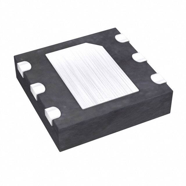
Package Information
6 TDFN-EP
Package Code
T633+2
Outline Number
21-0137
Land Pattern Number
90-0058
Thermal Resistance, Single-Layer Board:
Junction to Ambient (θJA)
Junction to Case (θJC)
Thermal Resistance, Four-Layer Board:
Junction to Ambient (θJA)
55°C/W
9°C/W
42°C/W
Junction to Case (θJC)
9°C/W
For the latest package outline information and land patterns (footprints), go to www.maximintegrated.com/packages. Note that a “+”,
“#”, or “-” in the package code indicates RoHS status only. Package drawings may show a different suffix character, but the drawing
pertains to the package regardless of RoHS status.
Package thermal resistances were obtained using the method described in JEDEC specification JESD51-7, using a four-layer board.
For detailed information on package thermal considerations, refer to www.maximintegrated.com/thermal-tutorial.
Electrical Characteristics
(TA = -40°C to +85°C.) (Note 1)
PARAMETER
Supply Voltage
SYMBOL
VCC
Active Supply Current
ICC
Standby Supply Current
ICCS
Computation Current
ICMP
CONDITIONS
MIN
DS28C36
2.97
DS28C36B
2.2
(Note 2)
(Note 3)
TYP
MAX
UNITS
3.3
3.63
V
300
µA
250
µA
7.5
mA
0.4
V
GPIO
Output Low
PIOVOL
Input Low
PIOVIL
-0.3
VCC x
0.3
V
Input High
PIOVIH
VCC x
0.7
VCC +
0.3
V
-10
-1
+10
+1
µA
Leakage current
IL
DS28C36
DS28C36B
ECC ENGINE
Generate ECDSA Signature Time
tGES
50
ms
Generate ECC Key Pair
tGKP
100
ms
Verify ECDSA Signature or Compute
ECDH Time
tVES
150
ms
tCMP
3
ms
SHA-256 ENGINE
Computation Time (HMAC or RNG)
www.maximintegrated.com
Maxim Integrated │ 2
�ABRIDGED DATA SHEET
DS28C36
DeepCover Secure Authenticator
Electrical Characteristics (continued)
(TA = -40°C to +85°C.) (Note 1)
PARAMETER
SYMBOL
CONDITIONS
MIN
TYP
MAX
UNITS
EEPROM
W/E Endurance
NCY
Read Memory Time
tRM
Write Memory Time
tWM
Data Retention
tDR
I2C SCL AND SDA PINS (Note 6)
(Note 4)
100K
1
15
TA = +85°C (Note 5)
10
Low-Level Input Voltage
VIL
-0.3
High-Level Input Voltage
VIH
0.7 ×
VCC
Hysteresis of Schmitt Trigger Inputs
VHYS
VOL
Output Fall Time from VIH(MIN) to
VIL(MAX) with a Bus Capacitance from
10pF to 400pF
tOF
(Note 7)
Pulse Width of Spikes that are
Suppressed by the Input Filter
tSP
(Note 7)
II
Input Capacitance
CI
SCL Clock Frequency
Hold Time (Repeated) START Condition
fSCL
tLOW
High Period of the SCL Clock
tHIGH
DS28C36B (Note 8)
-1
+1
(Note 9)
(Note 10)
Data Hold Time
tHD:DAT
(Notes 7, 10, 11)
Data Setup Time
tSU:DAT
(Notes 10, 12)
Warm-Up Time
www.maximintegrated.com
tBUF
tOSCWUP
10
DS28C36
DS28C36B
DS28C36
DS28C36B
tSU:STO
CB
50
(Notes 9, 13)
(Note 14)
DS28C36
DS28C36B
0
0
0.6
0.45
1.3
0.65
0.6
0.35
0.6
0.35
V
V
V
ns
+10
tSU:STA
Bus Free Time Between a STOP and
START Condition
Capacitive Load for Each Bus Line
30
DS28C36
DS28C36B
DS28C36
DS28C36B
DS28C36
DS28C36B
DS28C36
DS28C36B
DS28C36
DS28C36B
DS28C36
DS28C36B
ms
V
-10
Setup Time for a Repeated START
Condition
Setup Time for STOP Condition
VCC +
0.3
DS28C36
tHD:STA
Low Period of the SCL Clock
0.3 ×
VCC
0.4
(Note 7)
ms
years
0.05 ×
VCC
(Note 7)
Low-Level Output Voltage at 4mA Sink
Current
Input Current with an Input Voltage
Between 0.1VCCmax and 0.9VCCmax
—
ns
µA
pF
0.4
1
MHz
µs
µs
µs
µs
0.9
0.35
100
0.6
0.35
1.3
0.6
µs
ns
µs
µs
400
0.25
1.0
pF
ms
Maxim Integrated │ 3
�ABRIDGED DATA SHEET
DS28C36
DeepCover Secure Authenticator
Electrical Characteristics (continued)
(TA = -40°C to +85°C.) (Note 1)
Note 1: Limits are 100% production tested at TA = +25°C and/or TA = +85°C. Limits over the operating temperature range and
relevant supply voltage range are guaranteed by design and characterization. Typical values at +25°C.
Note 2: Operating current continuously reading memory at 400kHz with < 25ns rise and fall times on SDA and SCL.
Note 3: Average current drawn from VCC during EEPROM read, EEPROM write, RNG calculation, SHA-256 calculation, or ECDSA calculation.
Note 4: Write-cycle endurance is tested in compliance with JESD47H.
Note 5: Data retention is rested in compliance with JESD47H.
Note 6: All I2C timing values are referred to VIH(MIN) and VIL(MAX) levels.
Note 7: Guaranteed by design and/or characterization only. Not production tested.
Note 8: I/O pins of the DS28C36B do not obstruct the SDA and SCL lines if VCC is switched off.
Note 9: System requirement.
Note 10: tLOW min = tHD:DAT max + tEDGE max + tSU:DAT min, where tEDGE is rise or fall time. For the DS28C36, tEDGE max = 300ns;
for the DS28C36B, tEDGE max = 200ns. Values greater than these can be accommodated by extending tLOW accordingly.
Note 11: The DS28C36 provides a hold time of at least 100ns for the SDA signal (referred to the VIH(MIN) of the SCL signal) to bridge
the undefined region of the falling edge of SCL. The master can provide a hold time of 0ns when writing to the device.
Note 12: The DS28C36 can be used in a standard-mode I2C bus system, but the requirement tSU:DAT ≥ 250ns must then be met
(I2C bus specification Rev. 03, 19 June 2007).
Note 13: CB = total capacitance of one bus line in pF. The maximum bus capacitance allowable can vary from this value depending
on the actual operating voltage and frequency of the application (I2C bus specification Rev. 03, 19 June 2007).
Note 14: I2C communication should not take place for max tOSCWUP time following a power-on reset.
www.maximintegrated.com
Maxim Integrated │ 4
�ABRIDGED DATA SHEET
DS28C36
DeepCover Secure Authenticator
Pin Configuration
TOP VIEW
SCL 1
6 VCC
SDA
2
DS28C36
5 PIOA
GND
3
EP*
4 PIOB
TDFN-EP
(3mm x 3mm)
Pin Description
PIN
NAME
1
SCL
I2C CLK. Connect to VCC with a pullup resistor.
2
SDA
I2C Data. Connect to VCC with a pullup resistor.
3
GND
Ground
4
PIOB
General-Purpose IO
5
PIOA
General-Purpose IO
6
VCC
Supply Voltage
—
EP
www.maximintegrated.com
FUNCTION
Exposed Pad. Solder evenly to the board’s ground plane for proper operation. Refer to Application
Note 3273: Exposed Pads: A Brief Introduction for additional information.
Maxim Integrated │ 5
�ABRIDGED DATA SHEET
DS28C36
DeepCover Secure Authenticator
Typical Application Circuit
3.3V
RP2
RP1
RP4
DS28C36
VCC
µC
RP3
VCC
I2C
PORT
SDA
SCL
PIOA
PIOB
IO
IO
GND
GND
Ordering Information
PART
TEMP RANGE
PIN-PACKAGE
DS28C36Q+T†
-40°C to +85°C
6 TDFN-EP*
(2.5k pcs)
DS28C36BQ+T
-40°C to +85°C
6 TDFN-EP*
(2.5k pcs)
+Denotes a lead(Pb)-free/RoHS-compliant package.
T= Tape and reel.
*EP = Exposed pad.
†Not recommended for new designs.
www.maximintegrated.com
Maxim Integrated │ 6
�ABRIDGED DATA SHEET
DS28C36
DeepCover Secure Authenticator
Revision History
REVISION
NUMBER
REVISION
DATE
PAGES
CHANGED
0
6/16
Initial release
1
10/18
Updated Electrical Characteristics and Notes, Typical Operating Conditions,
authenticated SHA2 Write Memory HMAC input tables, and general corrections
1–63
2
1/19
Added indications of GPIO volatility in the Memory Resources section, Table 1,
and power-up states in Table 5
7, 10
3
12/20
Updated Package Information
DESCRIPTION
—
2
For pricing, delivery, and ordering information, please visit Maxim Integrated’s online storefront at https://www.maximintegrated.com/en/storefront/storefront.html.
Maxim Integrated cannot assume responsibility for use of any circuitry other than circuitry entirely embodied in a Maxim Integrated product. No circuit patent licenses
are implied. Maxim Integrated reserves the right to change the circuitry and specifications without notice at any time. The parametric values (min and max limits)
shown in the Electrical Characteristics table are guaranteed. Other parametric values quoted in this data sheet are provided for guidance.
Maxim Integrated and the Maxim Integrated logo are trademarks of Maxim Integrated Products, Inc.
© 2020 Maxim Integrated Products, Inc. │ 7
�


 工商网监
湘ICP备2023018690号
工商网监
湘ICP备2023018690号

