DS3065WP
3.3V, 8Mb, Nonvolatile SRAM with Clock
General Description
Features
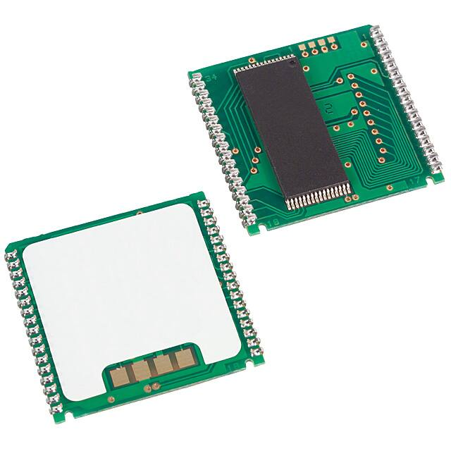
The DS3065WP consists of a static RAM, a nonvolatile
(NV) controller, and a real-time clock (RTC). These components are packaged on a surface-mount substrate
and require post-assembly attachment of a DS9034IPCX+ battery cap. Whenever VCC is applied to the
module, it powers the clock and SRAM from the external
power source, and allows the contents of the clock registers or SRAM to be modified. When VCC is powered
down or out of tolerance, the controller write protects the
memory contents and powers the clock and SRAM from
the battery.
S Reflowable, 34-Pin PowerCap Package
S Integrated RTC
S Unconditionally Write Protects the Clock and
SRAM When VCC is Out of Tolerance
S Automatically Switches to Battery Supply When
VCC Power Failures Occur
S Extended Industrial Temperature Range (-40NC to
+85NC)
S Underwriters Laboratories Recognized
Applications
RAID Systems and Servers/Gaming
POS Terminals/Fire Alarms
Industrial Controllers/PLCs
Data-Acquisition Systems
Routers/Switches
Ordering Information
PART
DS3065WP-100IND+
TEMP RANGE
SPEED (ns)
SUPPLY VOLTAGE (V)
PIN-PACKAGE
-40NC to +85NC
100
3.3 Q0.3
34 PowerCap Module
Typical Operating Circuit
CE
CE
WR
WE
RD
OE
CS
CS
DS3065WP
1024k x 8
NV SRAM
AND RTC
MICROPROCESSOR
OR DSP
DATA
8 BITS
ADDRESS
20 BITS
DQ0–DQ7
A0–A19
For pricing, delivery, and ordering information, please contact Maxim Direct at
1-888-629-4642, or visit Maxim Integrated’s website at www.maximintegrated.com.
19-5450; Rev 0; 7/10
�DS3065WP
3.3V, 8Mb, Nonvolatile SRAM with Clock
ABSOLUTE MAXIMUM RATINGS
Lead Temperature (soldering, 10s).................................+260NC
(intended for minor rework/touchup purposes only)
Soldering Temperature (reflow).......................................+260NC
Voltage Range on Any Pin Relative to Ground.....-0.3V to +4.6V
Operating Temperature Range........................... -40NC to +85NC
Storage Temperature Range............................. -55NC to +125NC
Stresses beyond those listed under “Absolute Maximum Ratings” may cause permanent damage to the device. These are stress ratings only, and functional
operation of the device at these or any other conditions beyond those indicated in the operational sections of the specifications is not implied. Exposure to absolute
maximum rating conditions for extended periods may affect device reliability.
RECOMMENDED OPERATING CONDITIONS
(TA = -40NC to +85NC, unless otherwise noted.) (Note 1)
MIN
TYP
MAX
UNITS
Supply Voltage
PARAMETER
SYMBOL
VCC
CONDITIONS
3.0
3.3
3.6
V
Logic 1 Input
VIH
2.2
VCC
V
Logic 0 Input
VIL
0.0
0.4
V
DC ELECTRICAL CHARACTERISTICS
(VCC = 3.3V Q0.3V, TA = -40NC to +85NC, unless otherwise noted.)
PARAMETER
SYMBOL
Input Leakage Current
CONDITIONS
IIL
MIN
MAX
UNITS
-1.0
+1.0
FA
+1.0
I/O Leakage Current
IIO
IOH
VCE = VCS = VCC
VOH = 2.4V
-1.0
Output-Current High
IOL
VOL = 0.4V
2.0
Output-Current Low
Standby Current
Operating Current
Write-Protection Voltage
TYP
-1.0
FA
mA
mA
ICCS1
VCE = VCS = 2.2V
0.6
2.0
ICCS2
VCE = VCS = VCC - 0.2V
0.6
1.5
ICCO1
tRC = 200ns, outputs open
50
mA
2.8
2.9
3.0
V
MIN
TYP
MAX
UNITS
VTP
mA
PIN CAPACITANCE
(TA = +25NC, unless otherwise noted.)
PARAMETER
Input Capacitance
Input/Output Capacitance
SYMBOL
CONDITIONS
CIN
Not production tested
15
pF
COUT
Not production tested
15
pF
AC ELECTRICAL CHARACTERISTICS
(VCC = 3.3V Q0.3V, TA = -40NC to +85NC, unless otherwise noted.)
PARAMETER
Read Cycle Time
Access Time
OE to Output Valid
RTC OE to Output Valid
SYMBOL
MIN
TYP
MAX
100
tRC
UNITS
ns
tACC
100
ns
tOE
50
ns
tOEC
60
ns
CE or CS to Output Valid
tCO
OE or CE or CS to Output Active
tCOE
2
CONDITIONS
100
(Note 2)
5
ns
ns
Maxim Integrated
�DS3065WP
3.3V, 8Mb, Nonvolatile SRAM with Clock
AC ELECTRICAL CHARACTERISTICS (continued)
(VCC = 3.3V Q0.3V, TA = -40NC to +85NC, unless otherwise noted.)
PARAMETER
SYMBOL
Output High Impedance from
Deselection
tOD
Output Hold from Address
tOH
Write Cycle Time
tWC
Write Pulse Width
tWP
Address Setup Time
tAW
CONDITIONS
MIN
TYP
(Note 2)
(Note 3)
MAX
UNITS
40
ns
5
ns
100
ns
75
ns
0
ns
tWR1
(Note 4)
5
tWR2
(Note 5)
20
Output High Impedance from WE
tODW
(Note 2)
Output Active from WE
Data Setup Time
tOEW
(Note 2)
5
ns
tDS
(Note 6)
40
ns
tDH1
(Note 4)
0
tDH2
(Note 5)
20
Write Recovery Time
Data Hold Time
Chip-to-Chip Setup Time
ns
40
ns
40
tCCS
ns
ns
POWER-DOWN/POWER-UP TIMING
(TA = -40NC to +85NC, unless otherwise noted.)
PARAMETER
SYMBOL
VCC Fail Detect to CE, CS, and
WE Inactive Time
tPD
CONDITIONS
MIN
TYP
(Note 7)
MAX
UNITS
1.5
Fs
VCC Slew from VTP to 0V
tF
150
Fs
VCC Slew from 0V to VTP
tR
150
Fs
VCC Valid to CE, CS, and WE
Inactive
tPU
2
ms
VCC Valid to End of Write
Protection
tREC
125
ms
MAX
UNITS
DATA RETENTION
(TA = +25NC, unless otherwise noted.)
PARAMETER
Expected Data-Retention Time
SYMBOL
tDR
CONDITIONS
(Notes 7, 8)
MIN
10
TYP
Years
AC TEST CONDITIONS
Voltage Range on Any Pin Relative to Ground: -0.3V to +4.6V
Input Pulse Levels: VIL = 0V, VIH = 2.7V
Input Pulse Rise and Fall Times: 5ns
Input and Output Timing Reference Level: 1.5V
Output Load: 1 TTL Gate + CL (100pF) including scope and jig
Maxim Integrated
3
�DS3065WP
3.3V, 8Mb, Nonvolatile SRAM with Clock
Read Cycle
tRC
ADDRESSES
VIH
VIH
VIH
VIL
VIL
VIL
VIH
CE
OR
CS
tOH
tACC
VIH
tCO
VIL
tOEC
tOE
VIH
OE
tOD
VIH
VIL
tOD
tCOE
tCOE
VOH
DOUT
VOL
VOH
OUTPUT
DATA VALID
VOL
(SEE NOTE 9.)
Write Cycle 1
tWC
ADDRESSES
CE
OR
CS
WE
VIH
VIL
tAW
VIL
VIL
tWP
VIH
VIL
tWR1
VIL
VIH
tOEW
tODW
DOUT
HIGH
IMPEDANCE
tDS
tDH1
VIH
DIN
VIH
VIL
VIH
VIL
VIL
VIH
DATA IN STABLE
VIL
(SEE NOTES 2, 3, 4, 6, 10–13.)
4
Maxim Integrated
�DS3065WP
3.3V, 8Mb, Nonvolatile SRAM with Clock
Write Cycle 2
tWC
VIH
VIL
ADDRESSES
tAW
CE
OR
CS
VIH
VIH
VIL
VIL
tWR2
tWP
VIH
VIH
VIL
VIL
VIL
VIH
WE
VIL
VIL
tODW
tCOE
DOUT
tDS
tDH2
VIH
VIH
DIN
DATA IN STABLE
VIL
VIL
(SEE NOTES 2, 3, 5, 6, 10–13.)
Power-Down/Power-Up Condition
VCC
VTP
tDR
~2.5V
tF
tR
tREC
tPD
CE,
WE
AND
CS
SLEWS WITH
VCC
tPU
VIH
BACKUP CURRENT
SUPPLIED FROM
LITHIUM BATTERY
(SEE NOTES 1, 7.)
Maxim Integrated
5
�DS3065WP
3.3V, 8Mb, Nonvolatile SRAM with Clock
Note 1: All voltages are referenced to ground.
Note 2: These parameters are sampled with a 5pF load and are not 100% tested.
Note 3: tWP is specified as the logical AND of CE with WE for SRAM writes, or CS with WE for RTC writes. tWP is measured from
the later of the two related edges going low to the earlier of the two related edges going high.
Note 4: tWR1 and tDH1 are measured from WE going high.
Note 5: tWR2 and tDH2 are measured from CE going high for SRAM writes or CS going high for RTC writes.
Note 6: tDS is measured from the earlier of CE or WE going high for SRAM writes, or from the earlier of CS or WE going high for
RTC writes.
Note 7: In a power-down condition, the voltage on any pin cannot exceed the voltage on VCC.
Note 8: The expected tDR is defined as accumulative time in the absence of VCC starting from the time power is first applied
by the user. Minimum expected data-retention time is based upon a single convection reflow exposure, followed by an
attachment of a new DS9034I-PCX+. This parameter is assured by component selection, process control, and design. It
is not measured directly during production testing.
Note 9: WE is high for any read cycle.
Note 10: VOE = VIH or VIL. If VOE = VIH during write cycle, the output buffers remain in a high-impedance state.
Note 11: If the CE or CS low transition occurs simultaneously with or later than the WE low transition, the output buffers remain in a
high-impedance state during this period.
Note 12: If the CE or CS high transition occurs prior to or simultaneously with the WE high transition, the output buffers remain in a
high-impedance state during this period.
Note 13: If WE is low or the WE low transition occurs prior to or simultaneously with the related CE or CS low transition, the output
buffers remain in a high-impedance state during this period.
6
Maxim Integrated
�DS3065WP
3.3V, 8Mb, Nonvolatile SRAM with Clock
Typical Operating Characteristics
(VCC = 3.3V, TA = +25NC, unless otherwise noted.)
5MHz CE-ACTIVATED
50% DUTY CYCLE
5MHz ADDRESS-ACTIVATED
100% DUTY CYCLE
5
4
1MHz CE-ACTIVATED
50% DUTY CYCLE
3
2
600
500
400
1
1MHz ADDRESS-ACTIVATED
100% DUTY CYCLE
0
4.0
3.1
3.2
3.3
3.4
3.5
3.2
3.0
3.4
3.6
SUPPLY VOLTAGE (V)
SUPPLY VOLTAGE (V)
SRAM OUTPUT-VOLTAGE HIGH
vs. OUTPUT CURRENT
SRAM OUTPUT-VOLTAGE LOW
vs. OUTPUT CURRENT
VCC = +3.0V,
TA = +25°C
0.4
OUTPUT VOLTAGE (V)
3.5
300
3.6
3.0
2.5
2.0
DS3065WP toc04
3.0
OUTPUT VOLTAGE (V)
VCE = VCS = VCC
TA = +25°C
700
SUPPLY CURRENT (µA)
6
DS3065WP toc03
SUPPLY CURRENT (mA)
7
800
DS3065WP toc01
8
POWER-SUPPLY CURRENT
vs. POWER-SUPPLY VOLTAGE
DS3065WP toc02
POWER-SUPPLY CURRENT
vs. POWER-SUPPLY VOLTAGE
VCC = +3.0V,
TA = +25°C
0.3
0.2
0.1
1.5
1.0
0
-2
-1
0
0
1
2
3
4
OUTPUT CURRENT (mA)
OUTPUT CURRENT (mA)
RTC OUTPUT-VOLTAGE HIGH
vs. OUTPUT CURRENT
RTC OUTPUT-VOLTAGE LOW
vs. OUTPUT CURRENT
VCC = +3.0V,
TA = +25°C
0.4
OUTPUT VOLTAGE (V)
3.5
OUTPUT VOLTAGE (V)
-3
3.0
2.5
2.0
5
DS3065WP toc06
4.0
-4
DS3065WP toc05
-5
VCC = +3.0V,
TA = +25°C
0.3
0.2
0.1
1.5
1.0
0
-5
-4
-3
-2
OUTPUT CURRENT (mA)
Maxim Integrated
-1
0
0
1
2
3
4
5
OUTPUT CURRENT (mA)
7
�DS3065WP
3.3V, 8Mb, Nonvolatile SRAM with Clock
Pin Configuration
TOP VIEW
34
A18
33
A17
3
32
A14
4
31
A13
VCC
5
30
A12
WE
6
29
A11
OE
7
28
A10
A19
1
A15
2
A16
CS
+
DS3065WP
CE
8
27
A9
DQ7
9
26
A8
DQ6
10
25
A7
DQ5
11
24
A6
DQ4
12
23
A5
DQ3
13
22
A4
DQ2
14
21
A3
DQ1
15
20
A2
19
A1
18
A0
DQ0
16
GND
17
GND
X1
BAT
X2
PowerCap MODULE
Pin Description
8
PIN
NAME
PIN
NAME
1
A19
Address Input 19
FUNCTION
18
A0
Address Input 0
FUNCTION
2
A15
Address Input 15
19
A1
Address Input 1
3
A16
Address Input 16
20
A2
Address Input 2
4
Active-Low RTC Chip-Select Input
21
A3
Address Input 3
5
CS
VCC
Supply Voltage
22
A4
Address Input 4
6
WE
Active-Low Write-Enable Input
23
A5
Address Input 5
7
OE
Active-Low Output-Enable Input
24
A6
Address Input 6
8
Active-Low SRAM Chip-Enable Input
25
A7
Address Input 7
9
CE
DQ7
Data Input/Output 7
26
A8
Address Input 8
10
DQ6
Data Input/Output 6
27
A9
Address Input 9
11
DQ5
Data Input/Output 5
28
A10
Address Input 10
12
DQ4
Data Input/Output 4
29
A11
Address Input 11
13
DQ3
Data Input/Output 3
30
A12
Address Input 12
14
DQ2
Data Input/Output 2
31
A13
Address Input 13
15
DQ1
Data Input/Output 1
32
A14
Address Input 14
16
DQ0
Data Input/Output 0
33
A17
Address Input 17
17
GND
Ground
34
A18
Address Input 18
Maxim Integrated
�DS3065WP
3.3V, 8Mb, Nonvolatile SRAM with Clock
Functional Diagram
DS9034I-PCX+
32.768kHz
CS
CS
A0–A3
WE
REAL-TIME
CLOCK
OE
CE
VTP REF
DELAY TIMING
CIRCUITRY
UNINTERRUPTED
POWER SUPPLY
FOR THE SRAM
AND RTC
VCC
VCC
CE
OE
WE
VSW REF
SRAM
DQ0–DQ7
REDUNDANT LOGIC
GND
CURRENT-LIMITING
RESISTOR
REDUNDANT
SERIES FET
BATTERY PROTECTION CIRCUITRY (UL RECOGNIZED)
DS3065WP
OE
WE
A0–A19
Maxim Integrated
9
�DS3065WP
3.3V, 8Mb, Nonvolatile SRAM with Clock
Detailed Description
The DS3065WP is an 8Mb (1024k x 8 bits), fully static,
nonvolatile (NV) memory similar in function and organization to the DS1265W NV SRAM, but containing an RTC.
The device NV SRAM constantly monitors VCC for an outof-tolerance condition. When such a condition occurs,
the lithium energy source is automatically switched on
and write protection is unconditionally enabled to prevent
data corruption. There is no limit to the number of write
cycles that can be executed, and no additional support
circuitry is required for microprocessor interfacing. This
device can be used in place of SRAM, EEPROM, or flash
components.
User access to either the SRAM or the RTC registers is
accomplished with a byte-wide interface and discrete
control inputs, allowing for a direct interface to many
3.3V microprocessor devices.
The RTC contains a full-function clock/calendar with an
RTC alarm, battery monitor, and power monitor. RTC
registers contain century, year, month, date, day, hours,
minutes, and seconds data in a 24-hour BCD format.
Corrections for day of the month and leap year are made
automatically.
The RTC registers are double-buffered into an internal
and external set. The user has direct access to the external set. Clock/calendar updates to the external set of
registers can be disabled and enabled to allow the user
to access static data. Assuming the internal oscillator is
on, the internal registers are continually updated, regardless of the state of the external registers, assuring that
accurate RTC information is always maintained.
The device constantly monitors the voltage of the internal
battery. The battery-low flag (BLF) in the RTC FLAGS
register is not writable and should always be a 0 when
read. Should a 1 ever be present, the battery voltage is
below ~ 2V and the contents of the clock and SRAM are
questionable.
The device module is constructed on a standard 34-pin
PowerCap substrate.
SRAM Read Mode
The device executes an SRAM read cycle whenever CS
(RTC chip select) and WE (write enable) are inactive
(high) and CE (SRAM chip enable) is active (low). The
unique address specified by the 20 address inputs
(A0–A19) defines which of the 1,048,576 bytes of SRAM
data is to be accessed. Valid data is available to the
eight data-output drivers within tACC (access time) after
the last address input signal is stable, provided that CE
and OE (output enable) access times are also satisfied.
If CE and OE access times are not satisfied, data access
must be measured from the later occurring signal (CE or
OE), and the limiting parameter is either tCO for CE or
tOE for OE rather than address access.
SRAM Write Mode
The device executes an SRAM write cycle whenever CS
is inactive (high) and the CE and WE signals are active
(low) after address inputs are stable. The later-occurring
falling edge of CE or WE determines the start of the write
cycle. The write cycle is terminated by the earlier rising
edge of CE or WE. All address inputs must be kept valid
throughout the write cycle. WE must return to the high
state for a minimum recovery time (tWR) before another
cycle can be initiated. The CS and OE control signal
should be kept inactive (high) during SRAM write cycles
to avoid bus contention. However, if the output drivers
have been enabled (CE and OE active), WE disables the
outputs in tODW from its falling edge.
Table 1. RTC/Memory Operational Truth Table
CS
0
WE
1
CE
1
OE
0
MODE
ICC
RTC Read
Active
OUTPUTS
Active
0
1
1
1
RTC Read
Active
High Impedance
0
0
1
X
RTC Write
Active
High Impedance
1
1
0
0
SRAM Read
Active
Active
1
1
0
1
SRAM Read
Active
High Impedance
1
0
0
X
SRAM Write
Active
High Impedance
1
X
1
X
Standby
Standby
High Impedance
0
X
0
X
Invalid
(see Figure 2)
Active
Invalid
X = Don’t care.
10
Maxim Integrated
�DS3065WP
3.3V, 8Mb, Nonvolatile SRAM with Clock
Clock Operations
RTC Read Mode
The device executes an RTC read cycle whenever CE
(SRAM chip enable) and WE (write enable) are inactive
(high) and CS (RTC chip select) is active (low). The least
significant four address inputs (A0–A3) define which of
the 16 RTC registers is to be accessed (see Table 3).
Valid data is available to the eight data-output drivers
within tACC (access time) after the last address input
signal is stable, provided that CS and OE (output enable)
access times are also satisfied. If CS and OE access
times are not satisfied, data access must be measured
from the later-occurring signal (CS or OE) and the limiting parameter is either tCO for CS or tOEC for OE rather
than address access.
RTC Write Mode
The device executes an RTC write cycle whenever CE
is inactive (high) and the CS and WE signals are active
(low) after address inputs are stable. The later-occurring
falling edge of CS or WE determines the start of the write
cycle. The write cycle is terminated by the earlier rising
edge of CS or WE. All address inputs must be kept valid
throughout the write cycle. WE must return to the high
state for a minimum recovery time (tWR) before another
cycle can be initiated. The CE and OE control signals
should be kept inactive (high) during RTC write cycles
to avoid bus contention. However, if the output drivers
have been enabled (CS and OE active), WE disables the
outputs in tODW from its falling edge.
Clock Oscillator Mode
The oscillator can be turned off to minimize current
drain from the battery. The OSC bit is the MSB of the
SECONDS register (B7 of F9h). Setting OSC to 1 stops
the oscillator; setting OSC to 0 starts the oscillator. The
initial state of OSC is not guaranteed. When power is
applied for the first time, the OSC bit should be enabled.
Reading the Clock
When reading the RTC data, it is recommended to halt
updates to the external set of double-buffered RTC registers. This puts the external registers into a static state,
allowing the data to be read without register values
changing during the read process. Normal updates to
the internal registers continue while in this state.
External updates are halted by writing a 1 to the read
bit (R). As long as a 1 remains in the R bit, updating is
inhibited. After a halt is issued, the registers reflect the
RTC count (day, date, and time) that was current at the
moment the halt command was issued. Normal updates
to the external set of registers resume within one second
after the R bit is set to 0 for a minimum of 500Fs. The R bit
must be 0 for a minimum of 500Fs to ensure the external
registers have fully updated.
Setting the Clock
As with a clock read, it is also recommended to halt
updates prior to setting new time values. Setting the write
bit (W) to 1 halts updates of the external RTC registers
8h–Fh. After setting the W bit to 1, the RTC registers can
be loaded with the desired count (day, date, and time)
in BCD format. Setting the W bit to 0 then transfers the
values written to the internal registers and allows normal
clock operation to resume.
Using the Clock Alarm
The alarm settings and control for the device reside
within RTC registers 2h–5h. The INTERRUPTS register
(6h) contains two alarm-enable bits: alarm flag enable
(AE) and alarm in backup-mode enable (ABE).
The alarm can be programmed to activate on a specific
day of the month or repeat every day, hour, minute, or
second. Alarm mask bits AM[4:1] control the alarm mode
(Table 2). Configurations not listed in the table default to
the once-per-second mode to notify the user of an incorrect alarm setting.
Table 2. Alarm Mask Bits
AM4
AM3
AM2
AM1
1
1
1
1
Once per second
1
1
1
0
When seconds match
1
1
0
0
When minutes and seconds match
1
0
0
0
When hours, minutes, and seconds match
0
0
0
0
When date, hours, minutes, and seconds match
Maxim Integrated
ALARM RATE
11
�DS3065WP
3.3V, 8Mb, Nonvolatile SRAM with Clock
VTP
VCC
ABE, AE
AF
Figure 1. Battery-Backup Mode Alarm Waveforms
When the RTC register values match alarm register settings, the alarm flag (AF) is set to 1.
The AE and ABE bits are reset to 0 during the power-up
transition, but an alarm generated during power-up sets
AF to 1. Therefore, the AF bit can be read after system
power-up to determine if an alarm was generated during
the power-up sequence. Figure 1 illustrates alarm timing
during battery-backup mode and power-up states.
Clock Accuracy
The DS3065WP and DS9034I-PCX+ are each individually
tested for accuracy. Once mounted together, the module
typically keeps time accuracy to within Q1.53 minutes
per month (35ppm) at +25NC and does not require
additional calibration. For this reason, methods of field
clock calibration are not available and not necessary.
The electrical environment also affects clock accuracy,
and caution should be taken to place the component in
the lowest level EMI section of the PCB layout. For additional information, refer to Application Note 58: Crystal
Considerations with Dallas Real-Time Clocks (RTCs).
Power-On Default States
Upon each application of power to the device, the following register bits are automatically set to 0: WDS = 0,
BMB[4:0] = 0, RB0 = 0, RB1 = 0, AE = 0, ABE = 0. All
other RTC bits are undefined.
12
Data-Retention Mode
The device provides full functional capability for VCC
greater than 3.0V and write protects by 2.8V. Data is
maintained in the absence of VCC without additional support circuitry. The NV SRAM constantly monitors VCC.
Should the supply voltage decay, the NV SRAM automatically write protects itself. All inputs become don’t
care, and all data outputs become high impedance. As
VCC falls below approximately 2.5V (VSW), the powerswitching circuit connects the lithium energy source to
the clock and SRAM to maintain time and retain data.
During power-up, when VCC rises above VSW, the power-switching circuit connects external VCC to the clock
and SRAM and disconnects the lithium energy source.
Normal clock or SRAM operation can resume after VCC
exceeds VTP for a minimum duration of tREC.
Freshness Seal
When the DS9034I-PCX+ battery cap is first attached to
a DS3065WP base, the RTC oscillator is disabled and
the lithium battery is electrically disconnected, guaranteeing that no battery capacity has been consumed during transit or storage.
When VCC is first applied at a level greater than VTP,
the lithium battery is enabled for backup operation. The
user is required to enable the oscillator (MSB of the
SECONDS register) and initialize the required RTC registers for proper timekeeping operation.
Maxim Integrated
�DS3065WP
3.3V, 8Mb, Nonvolatile SRAM with Clock
Table 3. RTC Register Map
ADDR
DATA
B7
B6
xxxxEh
X
X
xxxxDh
X
X
xxxxCh
X
FT
xxxxBh
X
X
xxxxAh
X
xxxx8h
OSC
W
R
10 CENTURY
xxxx7h
Y
Y
Y
Y
Y
Y
Y
Y
xxxx6h
AE
Y
ABE
Y
Y
Y
Y
Y
xxxx5h
AM4
Y
10 DATE
xxxx4h
AM3
Y
10 HR
xxxx3h
AM2
xxxx2h
AM1
xxxxFh
xxxx9h
B5
B4
B3
10 YEAR
X
10 MO
10 DATE
X
X
B2
B1
B0
FUNCTION
RANGE
YEAR
YEAR
00–99
MONTH
MONTH
01–12
DATE
DATE
01–31
X
DAY
01–07
HOUR
HOUR
00–23
10 MINUTES
MINUTES
MINUTES
00–59
10 SECONDS
SECONDS
SECONDS
00–59
CONTROL
00–39
Unused
—
INTERRUPTS
—
DATE
ALARM
DATE
01–31
HOURS
ALARM
HOURS
00–23
10 MINUTES
MINUTES
ALARM
MINUTES
00–59
10 SECONDS
SECONDS
ALARM
SECONDS
00–59
10 HOUR
DAY
CENTURY
xxxx1h
Y
Y
Y
Y
Y
Y
Y
Y
Unused
—
xxxx0h
WF
AF
0
BLF
0
0
0
0
FLAGS
—
x=
Don’t care address bits
X=
Unused; read/writable under write and read bit control
Y=
Unused; read/writable without write and read bit control
0=
Reads as 0 and cannot be changed
FT =
OSC =
W=
R=
AE =
ABE =
AM[4:1] =
Read bit
Alarm flag enable
Alarm in backup-mode enable
Alarm mask bits
Frequency test bit
WF =
Watchdog flag
Oscillator start/stop bit
AF =
Alarm flag
Write bit
Maxim Integrated
BLF =
Battery-low flag
13
�DS3065WP
3.3V, 8Mb, Nonvolatile SRAM with Clock
CE
VIH
VIH
tCCS
tCCS
VIH
CS
VIH
Figure 2. SRAM/RTC Data Bus Control
Applications Information
Power-Supply Decoupling
To achieve the best results when using the device,
decouple the power supply with a 0.1FF capacitor.
Use a high-quality, ceramic, surface-mount capacitor
if possible. Surface-mount components minimize lead
inductance, which improves performance, and ceramic capacitors tend to have adequate high-frequency
response for decoupling applications.
Avoiding Data Bus Contention
Care should be taken to avoid simultaneous access of
the SRAM and RTC devices (see Figure 2). Any chipenable overlap violates tCCS and can result in invalid
and unpredictable behavior.
14
Recommended Cleaning Procedures
The device can be cleaned using aqueous-based cleaning solutions. No special precautions are needed when
cleaning boards containing a DS3065WP module, provided that the cleaning and subsequent drying process
is completed prior to the DS9034I-PCX+ attachment.
DS3065W modules are recognized by Underwriters
Laboratories (UL) under file E99151.
Package Information
For the latest package outline information and land patterns, go
to www.maximintegrated.com/packages. Note that a “+”, “#”,
or “-” in the package code indicates RoHS status only. Package
drawings may show a different suffix character, but the drawing
pertains to the package regardless of RoHS status.
PACKAGE
TYPE
PACKAGE
CODE
OUTLINE
NO.
LAND
PATTERN NO.
34 PCAP
—
21-0246
See the
outline no.
21-0246
Maxim Integrated
�DS3065WP
3.3V, 8Mb, Nonvolatile SRAM with Clock
Revision History
REVISION
NUMBER
REVISION
DATE
0
7/10
DESCRIPTION
Initial release
PAGES
CHANGED
—
Maxim Integrated cannot assume responsibility for use of any circuitry other than circuitry entirely embodied in a Maxim Integrated product. No circuit patent
licenses are implied. Maxim Integrated reserves the right to change the circuitry and specifications without notice at any time. The parametric values (min and
max limits) shown in the Electrical Characteristics table are guaranteed. Other parametric values quoted in this data sheet are provided for guidance.
Maxim Integrated 160 Rio Robles, San Jose, CA 95134 USA 1-408-601-1000�
© 2010
Maxim Integrated Products, Inc.�
15
Maxim Integrated and the Maxim Integrated logo are trademarks of Maxim Integrated Products, Inc.
�


 工商网监
湘ICP备2023018690号
工商网监
湘ICP备2023018690号
