as
DS32kHz
32.768kHz Temperature-Compensated
Crystal Oscillator
www.maxim-ic.com
GENERAL DESCRIPTION
The DS32kHz is a temperature-compensated
crystal oscillator (TCXO) with an output
frequency of 32.768kHz. This device addresses
applications
requiring
better
timekeeping
accuracy, and can be used to drive the X1 input
of most Dallas Semiconductor real-time clocks
(RTCs), chipsets, and other ICs containing
RTCs. This device is available in commercial
(DS32kHz)
and
industrial
(DS32kHz-N)
temperature versions.
APPLICATIONS
GPS Receivers
Telematics
Network Timing and Synchronization in Servers,
Routers, Hubs, and Switches
Automatic Power Meters
FEATURES
Accurate to ±4 Minutes/Year (-40°C to +85°C)
Accurate to ±1 Minute/Year (0°C to +40°C)
Battery Backup for Continuous Timekeeping
VBAT Operating Voltage: 2.7V to 5.5V with VCC
Grounded
VCC Operating Voltage: 4.5V to 5.5V
Operating Temperature Range:
0°C to +70°C (Commercial)
-40°C to +85°C (Industrial)
No Calibration Required
Low-Power Consumption
Surface Mountable Using BGA Package
UL Recognized
ORDERING INFORMATION
PART
DS32KHZ/DIP
DS32KHZN/DIP
DS32KHZS
DS32KHZS#
DS32KHZSN
DS32KHZSN#
DS32KHZ/WBGA+
DS32KHZN/WBGA+
TEMP
RANGE
0ºC to +70ºC
-40ºC to +85ºC
0ºC to +70ºC
0ºC to +70ºC
-40ºC to +85ºC
-40ºC to +85ºC
0ºC to +70ºC
-40ºC to +85ºC
PINPACKAGE
14 DIP
14 DIP
16 SO (0.300”)
16 SO (0.300”)
16 SO (0.300”)
16 SO (0.300”)
36 BGA
36 BGA
TOP MARK*
DS32KHZ
DS32KHZ-N
DS32KHZS
DS32KHZS
DS32KHZSN
DS32KHZSN
DS32KHZ
DS32KHZ-N
#Denotes a RoHS-compliant device that may include lead that is exempt
under the RoHS requirements. The lead finish is JESD97 category e3, and
is compatible with both lead-based and lead-free soldering processes.
*A “#” anywhere on the top mark denotes a RoHS-compliant device. An “N”
denotes an industrial device.
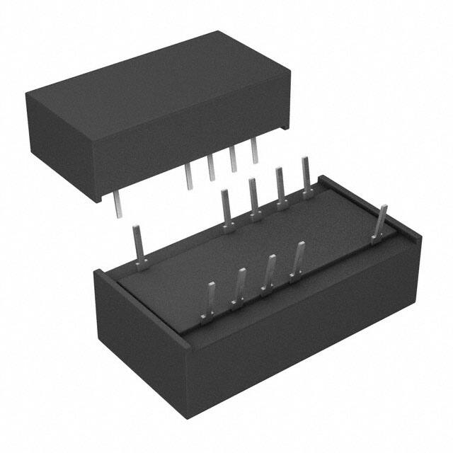
PIN CONFIGURATIONS
1 of 8
REV: 071521
�DS32kHz
ABSOLUTE MAXIMUM RATINGS
Voltage Range on Any Pin Relative to Ground………………………………………………………………-3.0V to +7.0V
Operating Temperature Range (Noncondensing)
Commercial:…………………………………………………………………………………………………..0°C to +70°C
Industrial:……………………………………………………………………………………………………-40°C to +85°C
Storage Temperature Range………………………………………………………………………………….-40°C to +85°C
Soldering Temperature (BGA, SO)……………………….See the Handling, PC Board Layout, and Assembly section.
Soldering Temperature, Leads (DIP)……………………………………………………..+260°C for 10 seconds (Note 1)
Stresses beyond those listed under “Absolute Maximum Ratings” may cause permanent damage to the device. These are stress ratings only,
and functional operation of the device at these or any other conditions beyond those indicated in the operational sections of the specifications is
not implied. Exposure to the absolute maximum rating conditions for extended periods may affect device reliability.
RECOMMENDED DC OPERATING CONDITIONS
(TA = -40°C to +85°C) (Note 1)
PARAMETER
SYMBOL
CONDITIONS
MIN
TYP
MAX
UNITS
5.5
3.5,
5.5
V
Power-Supply Voltage
VCC
(Note 2)
4.5
5.0
Battery Voltage
VBAT
(Notes 2, 3)
2.7
3.0
MIN
TYP
MAX
UNITS
150
220
µA
+50
nA
V
DC ELECTRICAL CHARACTERISTICS
(Over the operating range, unless otherwise specified.) (Note 1)
PARAMETER
SYMBOL
Active Supply Current
Battery Input-Leakage Current
ICC
IBATLKG
CONDITIONS
VBAT = 0V or
2.7V ≤ VBAT ≤ 3.5V
(Notes 3, 4)
VCC MIN ≤ VCC ≤ VCC MAX
-50
2.4
High Output Voltage (VCC)
VOH
IOH = -1.0mA (Note 2)
Low Output Voltage
VOL
IOL = 2.1mA (Note 2)
High Output Voltage (VBAT)
VOH
IOH = -0.1mA (Note 2)
Battery Switch Voltage
VSW
(Note 2)
V
0.4
2.4
V
V
VBAT
V
(VCC = 0V, TA = -40°C to +85°C.) (Note 1)
PARAMETER
SYMBOL
Active Battery Current
Battery Current During
Temperature Measurement
CONDITIONS
MIN
TYP
MAX
UNITS
4
µA
IBAT
VBAT = 3.3V (Notes 4, 5, 6)
1
IBATCNV
VBAT = 3.3V (Notes 4, 5, 7)
450
Note 1:
Limits at -40°C are guaranteed by design and are not production tested.
Note 2:
All voltages are referenced to ground.
Note 3:
VBAT must be no greater than 3.5V when the device is used in the dual-supply operating modes.
Note 4:
Typical values are at +25°C and 5.0V VCC, 3.0 VBAT, unless otherwise indicated.
Note 5:
These parameters are measured under no output load conditions.
Note 6:
This current is the active-mode current sourced from the backup supply/battery.
Note 7:
A temperature conversion lasts 122ms (typ) and occurs on power-up and then once every 64 seconds.
2 of 8
µA
�DS32kHz
AC TIMING CHARACTERISTICS
(Over the operating range, unless otherwise specified.)
PARAMETER
Output Frequency
SYMBOL
CONDITIONS
MIN
fOUT
TYP
MAX
32.768
0°C to +40°C
Industrial Device (N):
-40°C to +85°C
Commercial Device:
0°C to +70°C
UNITS
kHz
-2.0
+2.0
-7.5
+7.5
Frequency Stability vs.
Temperature
∆f/fO
Duty Cycle
tW/t
Cycle Time
tCYC
(Note 8)
30.518
µs
High/Low Time
tH/tL
(Note 8)
15.06
µs
Rise Time
tR
(Note 8)
200
ns
Fall Time
tF
(Note 8)
60
ns
(Note 8)
VCC = 5.0V or
VBAT = 3.0V, VCC = 0V
(Notes 4, 9)
1
seconds
+2.5
ppm/V
±1.0
ppm
Oscillator Startup Time
tOSC
Frequency Stability vs.
Operating Voltage
∆f/V
Crystal Aging (First Year)
∆f/fO
45
(Notes 4, 10)
Note 8:
These parameters are measured using a 15pF load.
Note 9:
Error is measured from the nominal supply voltage of whichever supply is powering the device.
Note 10:
After reflow.
Figure 1. DS32kHz Output Waveform
3 of 8
50
55
ppm
%
�DS32kHz
TYPICAL OPERATING CHARACTERISTICS
(VCC = 3.3V, TA = +25°C, unless otherwise noted.)
IBAT versus VBAT
ICC versus VCC
4.5
145
135
SUPPLY CURRENT (uA
SUPPLY CURRENT (uA
4
3.5
3
2.5
125
115
105
95
2
85
1.5
2.7
3.2
3.7
4.2
VBAT (V)
4.7
75
5.2
5.00
VCC (V)
5.25
7
6
12.5
47pF
V BAT
5
10.0
7.5
22pF
5.0
Deviation in ppm
SUPPLY CURRENT (uA
5.50
Frequency Deviation Versus Supply Voltage
IBAT vs. VBAT vs. output load
15.0
4.75
4.50
4
3
2
V CC
10pF
1
2.5
0pF
0
-1
0.0
2.7
3.2
3.7
4.2
VBAT
4.7
5.2
2.7
3.2
3.7
4.2
4.7
Supply Voltage (V)
4 of 8
5.2
�DS32kHz
PIN DESCRIPTION
PIN
NAME
FUNCTION
SO
BGA
DIP
1
C4, C5, D4, D5
12
32kHz
2
C2, C3, D2, D3
13
VCC
Primary Power Supply
1, 6–11, 14
N.C.
No Connection (Must be grounded)
4
GND
Ground
5
VBAT
+3V Nominal Supply Input. Used to operate the
device when VCC is absent.
3–12, 15, 16
13
14
A7, A8, B7, B8,
C7, C8, D7, D8
All remaining
balls
A4, A5, B4, B5
32.768kHz Push-Pull Output
Figure 2. Delta Time and Frequency vs. Temperature
20
0
0
Crystal +20ppm
Typical Crystal,
Uncompensated
-40
DS32kHz
Accuracy
Band
-60
-20
-80
-40
-100
-120
-60
Crystal -20ppm
-140
-160
Delta Time (Min/Year)
Delta Frequency (ppm)
-20
-80
-180
-200
-100
-40
-30
-20
-10
0
10
20
30
40
50
60
70
80
Temperature (°C)
FUNCTIONAL DESCRIPTION
The DS32kHz is a temperature-compensated crystal oscillator (TCXO) that outputs a 32,768Hz square wave.
While the DS32kHz is powered by either supply input, the device measures the temperature every 64 seconds and
adjusts the output frequency. The device requires four pins for operation: VCC, GND, VBAT, and 32kHz. (See
Figure 4 for connection schemes.) Power is applied through VCC and GND, while VBAT is used to maintain the
32kHz output in the absence of power. Once every 64 seconds, the DS32kHz measures the temperature and
adjusts the output frequency. The output is accurate to ±2ppm (±1 min/yr) from 0°C to +40°C and to ±7.5ppm
(±4 min/year) from -40°C to 0°C and from +40°C to +85°C.
5 of 8
�DS32kHz
The DS32kHz is packaged in a 36-pin ball grid array (BGA). It also is available in a 16-pin 0.300” SO and a 14-pin
encapsulated DIP (EDIP) module.
The additional PC board space required to add the DS32kHz as an option for driving a RTC is negligible in many
applications (see Figure 6) Therefore, adding the DS32kHz to new designs and future board revisions allows the
use of the DS32kHz where applications require improved timekeeping accuracy.
Figure 3. Block Diagram
VCC
Temperature
Measurement
VBAT
Dallas
Semiconductor
DS32kHz
Power Control
Power
Switching
Circuit
P
32.768kHz
N
GND
OPERATION
The DS32kHz module contains a quartz tuning-fork crystal and an IC. When power is first applied, and when the
device switches between supplies, the DS32kHz measures the temperature and adjusts the crystal load to
compensate the frequency. The power supply must remain at a valid level whenever a temperature measurement
is made, including when VCC is first applied. While powered, the DS32kHz measures the temperature once every
64 seconds and adjusts the crystal load.
The DS32kHz is designed to operate in two modes. In the dual-supply mode, a comparator circuit, powered by VCC,
monitors the relationship between the VCC and VBAT input levels. When VCC drops below a certain level compared to
VBAT, the device switches over to VBAT (Figure 4A). This mode uses VCC to conserve the battery connected to VBAT
while VCC is applied.
In the single-supply mode, VCC is grounded and the unit is powered by VBAT. Current consumption is less than VCC,
because the comparator circuit is unpowered (Figure 4B).
Figure 4A shows how the DS32kHz should be connected when using two power supplies. VCC should be between
4.5V and 5.5V, and VBAT should be between 2.7V and 3.5V. Figure 4B shows how the DS32kHz can be used when
only a single-supply system is available. VCC should be grounded and VBAT should then be held between 2.7V and
5.5V. The VBAT pin should be connected directly to a battery. Figure 4C shows a single-supply mode where VCC is
held at +5V. See the frequency stability vs. operating voltage for information about frequency error vs. supply
voltage.
6 of 8
�DS32kHz
Figure 4. Power-Supply Connections
4.5V - 5.5V
4.5V - 5.5V
2.7V - 3.3V
Vcc
Vcc
Vcc
Vbat
32.768kHz out
2.7V - 5.5V
Vbat
32.768kHz out
Vbat
32.768kHz out
GND
GND
GND
A
B
C
Figure 5 illustrates how a standard 32.768kHz crystal and the DS32kHz should be connected to address the
interchangeable option. Using this connection scheme and the recommended layout provides a solution, which
requires no hardware modifications. Only one device should be used at a time, and both layouts should be located
very close together if the recommended layout is not used.
The DS32kHz ICC and IBAT currents are specified with no output loads. Many RTC oscillator circuits use a quartz
crystal or resonator. Driving the oscillator circuit with the rail-to-rail output of the DS32kHz can increase the ICC and
IBAT currents significantly and increase the current consumption of the RTC as well. Figure 6 shows one circuit that
can be used to reduce the current consumption of a DS32kHz and an RTC. The values of R1 and C1 may vary
depending on the RTC used. However, values of 1.0MΩ and 100pF are recommended as a starting point. R2 is
used to shift the input waveform to the proper level. The recommended value for R2 is 33kΩ.
Figure 5. DS32kHz Connections
VCC
VBAT
32kHz out
X1 or Xin
32.768 Hz
DS32kHz
RTC
X2 or Xout
VCC
VBAT
A PC board can be laid out so that the RTC can use either the DS32kHz or a crystal
Figure 6. DS32kHz and RTC Connections
VCC
VBAT
DS32kHz
R1
1MΩ
VCC
C1
100pF
R2
33kΩ
X1
X2
RTC
VBAT
7 of 8
�DS32kHz
RELATED APPLICATION NOTES
(Go to www.maxim-ic.com/RTCapps to find these application notes and more.)
Application Note 58: Crystal Considerations with Dallas Real-Time Clocks
Application Note 701: Using the DS32kHz with Dallas RTCs
HANDLING, PC BOARD LAYOUT, AND ASSEMBLY
These packages contain a quartz tuning-fork crystal. Pick-and-place equipment may be used, but precautions
should be taken to ensure that excessive shocks are avoided. Ultrasonic cleaning should be avoided to prevent
damage to the crystal.
Avoid running signal traces under the package, unless a ground plane is placed between the package and the
signal line. All N.C. (no connect) pins must be connected to ground.
The BGA package may be reflowed as long as the peak temperature does not exceed +225°C. Peak reflow
temperature (≥ 220°C) duration should not exceed 10 seconds, and the total time above 200°C should not exceed
40 seconds (30 seconds nominal). For the SO package, refer to the IPC/JEDEC J-STD-020 specification for reflow
profiles. Exposure to reflow is limited to 2 times maximum. The DIP package can be wave-soldered, provided that
the internal crystal is not exposed to temperatures above +150°C.
Moisture sensitive packages are shipped from the factory dry-packed. Handling instructions listed on the package
label must be followed to prevent damage during reflow. Refer to the IPC/JEDEC J-STD-020 standard for moisturesensitive device (MSD) classifications.
THERMAL INFORMATION
PACKAGE TYPE
16-pin SO (300 mils)
36-pin BGA
THETA-JA
(°C/W)
73
43.9
THETA-JC
(°C/W)
23
18.4
PACKAGE INFORMATION
(For the latest package information, go to www.maxim-ic.com/DallasPackInfo.)
PACKAGE TYPE
DOCUMENT NO.
14-pin Encapsulated DIP
16-pin SO (300 mils)
36-pin BGA
56-G0001-002
56-G4009-001
56-G6023-001
8 of 8
Maxim/Dallas Semiconductor cannot assume responsibility for use of any circuitry other than circuitry entirely embodied in a Maxim/Dallas Semiconductor product.
No circuit patent licenses are implied. Maxim/Dallas Semiconductor reserves the right to change the circuitry and specifications without notice at any time.
Maxim Integrated Products, 120 San Gabriel Drive, Sunnyvale, CA 94086 408-737-7600
© 2006 Maxim Integrated Products • Printed USA
The Maxim log is a registered trademark of Maxim Integrated Products, Inc. The Dallas logo is a registered trademark of Dallas Semiconductor Corporation.
�