Rev 0; 4/06
Dual, 64-Position Nonvolatile Digital
Potentiometer with Buffered Outputs
The DS3908 contains two nonvolatile digital potentiometers with programmable-gain amplifiers buffering
the wiper outputs. The potentiometer position and
amplifier gain are controlled through an I2C-compatible
serial bus. The DS3908 operates in both 3.3V and 5V
systems and features a write-protect pin that locks the
position of the potentiometers and gain registers. Up to
eight DS3908s can be placed on a single I2C bus.
Features
♦ Two 64-Position Linear Taper Potentiometers
♦ Integral Wiper Buffering Amplifiers with
Selectable Gains of 1V/V, 2V/V, or 4V/V
♦ 100kΩ Potentiometer End-to-End Resistance
♦ Low Potentiometer Temperature Coefficient
♦ Nonvolatile Wiper and Gain Storage
♦ I2C-Compatible Interface
♦ Write-Protect Pin Prevents Accidental Field
Reprogramming
♦ 3V to 5.5V Supply Voltage Range
♦ -40°C to +85°C Operating Temperature Range
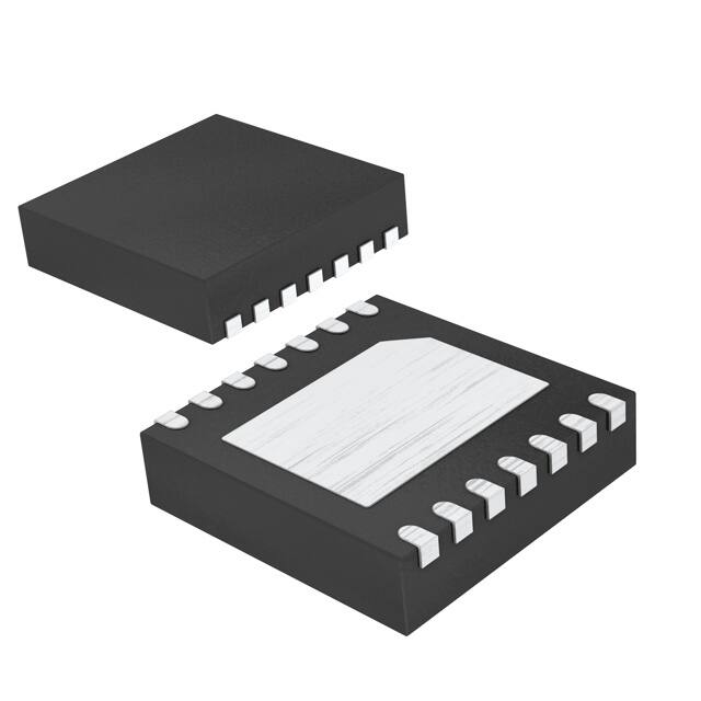
♦ 14-Pin TDFN Package
Applications
Ordering Information
Pin-Diode Biasing
PART
Power-Supply Calibration
DS3908N+
Cell Phones and PDAs
TEMP RANGE
PIN-PACKAGE
-40°C to +85°C
14 TDFN
+Denotes lead-free package.
Portable Electronics
Pin Configuration
Typical Operating Circuit
TOP VIEW
VCC
H0
DS3908
SDA
SCL
A0
A1
A2
WP
PGA0
V0
L0
I2C
INTERFACE
POT1
VOLTAGE
REFERENCE
NV ADJUSTABLE
REFERENCE
VOLTAGE
1
SCL
2
13 H1
A0
3
12 V1
A1
4
V1
L1
NV ADJUSTABLE
REFERENCE
VOLTAGE
11 L1
DS3908
H1
PGA1
14 VCC
SDA
+
POT0
A2
5
10 H0
WP
6
9
V0
GND
7
8
L0
TDFN (3mm x 3mm)
______________________________________________ Maxim Integrated Products
For pricing, delivery, and ordering information, please contact Maxim/Dallas Direct! at
1-888-629-4642, or visit Maxim’s website at www.maxim-ic.com.
1
DS3908
General Description
�DS3908
Dual, 64-Position Nonvolatile Digital
Potentiometer with Buffered Outputs
ABSOLUTE MAXIMUM RATINGS
Voltage on VCC, SDA, and SCL Relative to GND .....-0.5V to +6.0V
Voltage on A0, A1, A2, L0, L1, H0, H1, and WP Relative
to GND................-0.5V to (VCC + 0.5V) (not to exceed +6.0V)
Operating Temperature Range ...........................-40°C to +85°C
Programming Temperature Range .........................0°C to +70°C
Storage Temperature Range .............................-55°C to +125°C
Soldering Temperature ............Refer to J-STD-020 Specification
Stresses beyond those listed under “Absolute Maximum Ratings” may cause permanent damage to the device. These are stress ratings only, and functional
operation of the device at these or any other conditions beyond those indicated in the operational sections of the specifications is not implied. Exposure to
absolute maximum rating conditions for extended periods may affect device reliability.
RECOMMENDED OPERATING CONDITIONS
(TA = -40°C to +85°C.)
PARAMETER
Supply Voltage
Input Logic 1
(SCL, SDA, A0, A1, A2, WP)
Input Logic 0
(SCL, SDA, A0, A1, A2, WP)
SYMBOL
VCC
CONDITIONS
TYP
MAX
UNITS
+3.0
+5.5
V
VIH
0.7 x
VCC
VCC +
0.3
V
VIL
-0.3
0.3 x
VCC
V
-0.3
VCC +
0.3V
V
MAX
UNITS
Potentiometer Voltage
(L0, L1, H0, H1)
(Note 1)
MIN
VCC = +3.0V to +5.5V
DC ELECTRICAL CHARACTERISTICS
(VCC = +3.0V to +5.5V, TA = -40°C to +85°C.)
PARAMETER
Input Leakage
SYMBOL
CONDITIONS
IL
MIN
TYP
-1
+1
µA
2
mA
Standby Supply Current
ISTBY
VCC = 5.5V (Note 2)
Low-Level Output Voltage
(SDA)
VOL1
3mA sink current
0
0.4
VOL2
6mA sink current
0
0.6
I/O Capacitance
CI/O
WP Internal Pullup Resistance
RWP
V
10
pF
40
65
100
kΩ
MIN
TYP
MAX
UNITS
79
100
121
kΩ
ANALOG POTENTIOMETER CHARACTERISTICS
(VCC = +3.0V to +5.5V, TA = -40°C to +85°C.)
PARAMETER
SYMBOL
End-to-End Resistance
CONDITIONS
+25°C
Absolute Linearity
INL
(Notes 3, 4)
-0.6
+0.6
LSB
Relative Linearity
DNL
(Notes 4, 5)
-0.25
+0.25
LSB
End-to-End Temperature
Coefficient
2
_____________________________________________________________________
50
ppm/°C
�Dual, 64-Position Nonvolatile Digital
Potentiometer with Buffered Outputs
DS3908
PROGRAMMABLE-GAIN AMPLIFIER CHARACTERISTICS
(VCC = +3.0V to +5.5V, TA = -40°C to +85°C.)
PARAMETER
Common-Mode Input Voltage
Gain
SYMBOL
G
Output Voltage Range
VOUT
Power-Supply Rejection Ratio
PSRR
Output Source Current
Output Sink Current
CONDITIONS
CMVIN
TYP
0
MAX
UNITS
VCC - 1.5
V
RL ≥ 2kΩ, G = 1V/V
0.975
1
1.025
RL ≥ 2kΩ, G = 2V/V
1.925
2
2.05
RL ≥ 2kΩ, G = 4V/V
3.850
4
4.10
RL = 2kΩ, -1mA < IOUT < 1mA
0.3
60
IOUT:SOURCE
VOUT = 0V, Hx = Lx = 1V
IOUT:SINK
VOUT = 1V, Hx = Lx = 0V
Unity-Gain Frequency
fT
Gain = 1V/V, position 3Fh
Amplifier Capacitive Loading
CL
Input Offset Voltage
MIN
VCC - 0.3
90
VOS
-15
15
Output-Voltage Slew Rate
RL = 10kΩ, CL = 10pF
mA
mA
3.5
-9
-1mA < IOUT < 1mA
V
dB
MHz
100
Load Regulation
V/V
800
270
pF
+9
mV
2200
µV/mA
840
V/ms
MAX
UNITS
400
kHz
AC ELECTRICAL CHARACTERISTICS
(VCC = +3.0V to +5.5V, TA = -40°C to +85°C.) (See Figure 2.)
PARAMETER
SYMBOL
CONDITIONS
MIN
TYP
SCL Clock Frequency
fSCL
Bus Free Time between STOP
and START Conditions
tBUF
1.3
µs
Hold Time (Repeated) START
Condition
tHD:STA
0.6
µs
Low Period of SCL
tLOW
1.3
µs
High Period of SCL
tHIGH
0.6
Data Hold Time
tHD:DAT
0
Data Setup Time
tSU:DAT
100
ns
Start Setup Time
tSU:STA
0.6
µs
SDA and SCL Rise Time
SDA and SCL Fall Time
STOP Setup Time
SDA and SCL Capacitance
(Note 6)
µs
0.9
tR
(Note 7)
20 + 0.1CB
300
tF
(Note 7)
20 + 0.1CB
300
tSU:STO
0.6
CB
(Note 7)
EEPROM Write Time
tW
(Note 8)
Startup Time
tST
VCC = 3.0V
µs
ns
ns
µs
10
400
pF
17
ms
40
µs
_____________________________________________________________________
3
�Dual, 64-Position Nonvolatile Digital
Potentiometer with Buffered Outputs
DS3908
NONVOLATILE MEMORY CHARACTERISTICS
(VCC = +3.0V to +5.5V.)
PARAMETER
SYMBOL
CONDITIONS
EEPROM Write Cycles
MIN
At +70°C
MAX
UNITS
50,000
All voltages are referenced to ground.
ISTBY specified assuming control pins are connected as follows: WP must be disconnected or connected high. H terminal
connected to VCC, L terminal connected to GND, potentiometer position 1Dh, PGA is at 2V/V, A0 to A2 connected to VCC,
SDA and SCL connected to VCC, with no load.
Absolute linearity is used to measure expected wiper voltage as determined by wiper position in a voltage-divider
configuration.
This specification only refers to the potentiometers, and does not include the gain and offset error due to the PGA.
Relative linearity is used to determine the change of wiper voltage between two adjacent wiper positions in a voltagedivider configuration.
I2C interface timing shown is for fast-mode (400kHz) operation. This device is also backward-compatible with I2C standard-mode timing.
CB—total capacitance of one bus line in picofarads, timing referenced to 0.9 x VCC and 0.1 x VCC.
EEPROM write begins after a stop condition occurs.
Note 1:
Note 2:
Note 3:
Note 4:
Note 5:
Note 6:
Note 7:
Note 8:
Typical Operating Characteristics
(TA = +25°C, unless otherwise noted.)
STANDBY SUPPLY CURRENT
vs. TEMPERATURE
1.6
1.8
1.4
1.4
1.2
1.2
1.0
Hx = VCC, Lx = GND
A0 TO A2 = VCC
SDA, SCL = VCC
POT AT 1Dh
GAIN = 2V/V
NO LOAD
0.6
0.4
0.2
-40°C
4.0V
1.16200
1.16000
1.0
3.3V
0.8
0.6
3.5
1.15200
0.2
4.0
4.5
5.0
5.5
1.15000
-40
-15
VCC
10
35
60
1
85
100
TEMPERATURE (°C)
OUTPUT VOLTAGE vs. POT SETTING
VOL vs. IOUT:SINK
1.90000
VCC - VOH vs. IOUT:SOURCE
1
1
VCC - VOH (V)
VOL (V)
1.80000
1.70000
0.1
1.60000
+85°C +25°C
1.50000
1,000,000
10
DS3908 toc05
GAIN = 1V/V
Hx = 1V
Lx = 0.3V
10,000
SCL FREQUENCY (Hz)
10
DS3908 toc04
1.10000
1.00000
1.15600
1.15400
0
3.0
1.15800
0.4
0
OUTPUT VOLTAGE AT Vx (mA)
1.16400
DS3908 toc06
0.8
5.5V
1.6
ISTBY (mA)
ISTBY (mA)
2.0
ISTBY (mA)
+25°C
DS3908 toc02
+85°C
1.8
DS3908 toc01
2.0
STANDBY SUPPLY CURRENT
vs. SCL FREQUENCY
DS3908 toc03
STANDBY SUPPLY CURRENT
vs. SUPPLY VOLTAGE
0.1
+85°C +25°C
0.01
0.01
1.40000
1.30000
0
10
20
30
40
POT SETTING (DEC)
4
50
60
0.001
0.001
-40°C
-40°C
0.01
0.1
1
10
100
IOUT:SINK (mA)
_____________________________________________________________________
0.001
0.001
0.01
0.1
1
IOUT:SOURCE (mA)
10
100
�Dual, 64-Position Nonvolatile Digital
Potentiometer with Buffered Outputs
GAIN = 1V/V
0.20
0.15
0.4
0.15
-0.2
0.10
POT DNL (LSB)
POT INL (LSB)
0
0.05
0
-0.05
0.05
0
-0.05
-0.4
-0.10
-0.10
-0.6
-0.15
-0.15
-0.8
-0.20
-0.20
-1.0
-1.25
-15
10
35
60
85
-1.25
0
10
20
TEMPERATURE (°C)
30
40
+85°C
0.3
0.2
+25°C
-40°C
-0.1
-0.2
-0.3
-0.4
-0.5
GAIN = 1V/V
DATA OFFSET TO SHOW 0 AT 2V CMVIN
0.3
10
20
0.7
1.1
1.5
1.9
2.3
2.7
30
40
50
60
POT0 SETTING (DEC)
0.25
0.2
TYPICAL PGA OFFSET (mV)
0.4
0
0
TYPICAL PGA OFFSET
vs. TEMPERATURE
DS3908 toc10
0.6
0.1
60
POT0 SETTING (DEC)
TYPICAL PGA OFFSET
vs. COMMON-MODE INPUT VOLTAGE
0.5
50
DS3908 toc11
-40
GAIN = 1V/V
0.20
0.10
0.2
DS3908 toc09
0.6
POT DNL vs. SETTING
0.25
DS3908 toc08
VCC = 5V
0.8
POT INL vs. SETTING
0.25
DS3908 toc07
1.0
TYPICAL PGA OFFSET (mV)
NORMALIZED POT END-END RESISTANCE (Ω/Ω)
NORMALIZED POT END-END RESISTANCE
vs. TEMPERATURE
CMVIN = 0.3V
0.15
0.1
0.05
0
CMVIN = 2.0V
-0.05
CMVIN = 3.5V
-0.1
-0.15
-0.2
3.1
3.5
COMMON-MODE INPUT VOLTAGE (V)
-40
-15
10
35
60
85
TEMPERATURE (°C)
Pin Description
TDFN PIN
NAME
1
SDA
I2C Serial Data. Input/output for I2C data.
FUNCTION
2
SCL
I2C Serial Clock. Input for I2C clock.
3, 4, 5
A0, A1, A2
Address-Select Inputs. Determines I2C address. Device address is 1010A2A1A0. (See the I2C Slave
Address and Address Pins section for more details.)
6
WP
Write-Protect Input. Must be grounded to write to the registers. An internal pullup will lock the register
values if this pin is not connected.
7
GND
Ground Terminal
8, 11
L0, L1
Potentiometer Low Terminals. Voltages on these pins should remain between GND and VCC.
9, 12
V0, V1
Amplifier Outputs
10, 13
H0, H1
Potentiometer High Terminals. Voltages on these pins should remain between GND and VCC.
14
VCC
Supply Voltage Terminal
_____________________________________________________________________
5
DS3908
Typical Operating Characteristics (continued)
(TA = +25°C, unless otherwise noted.)
�Dual, 64-Position Nonvolatile Digital
Potentiometer with Buffered Outputs
DS3908
Functional Diagram
DS3908
EEPROM
POT0
F8h
VCC
VCC
H0
POT0 REGISTER
PGA0
SDA
SCL
A0
A1
V0
L0
I2C
F9h
POT1
INTERFACE
H1
POT1 REGISTER
A2
PGA1
FAh
L1
POT0/1 REGISTER
VCC
V1
1x, 2x, 4x GAIN
RWP
WP
FBh
G1
1x, 2x, 4x GAIN
GND
Detailed Description
The DS3908 contains two nonvolatile digital potentiometers with programmable-gain amplifiers buffering
the wiper outputs.
The potentiometers have 63 equally weighted (lineartaper) resistive elements, for a total of 64 taps. The
resistive elements are built using a low-temperaturedrift material, and have a typical 100kΩ end-to-end
resistance. This produces an output that is highly linear, with the highest and lowest taps connected to high
(Hx) and low (Lx) terminals, respectively. The potentiometers are independently controlled using an I2Ccompatible interface. Three address pins allow one of
eight slave addresses to be selected. The eight slave
addresses allow the DS3908 address to be customized
for applications with multiple I2C devices, and allow up
to eight DS3908s to be placed on the same I2C bus.
The potentiometer positions are saved in EEPROM, and
are recalled during each power-up to provide nonvolatile position settings. Once the settings are written,
the write-protect pin prevents accidental writes to the
potentiometers. The write-protection function is ideal for
6
G0
analog factory calibration because it prevents errant
transactions on the I2C bus from corrupting the settings
of the device. The WP pin contains an internal pullup
resistor that must be pulled low to write to the device.
The programmable-gain amplifiers can be independently set to one of three different gains—1V/V, 2V/V, or
4V/V. The amplifiers’ common-mode input range is from
ground to 1.5V below VCC, and the output is rail-to-rail
and capable of driving 1mA loads, 300mV from each
supply rail. The outputs are stable driving 100pF loads
for applications that require output filtering.
The addition of the amplifier to buffer the potentiometer
wiper offers distinct advantages over standard digital
potentiometers. The buffer provides a high-impedance
load for the potentiometer and a low-impedance voltage output. This improves the linearity of the output
voltage for systems that load the potentiometer by eliminating the changes in current through both the potentiometer and the wiper impedance. It also allows
voltage gain from the potentiometer input to the output.
Because the amplifiers are integrated into the DS3908,
this is done without increasing the footprint of the
design or the complexity of the PC board.
_____________________________________________________________________
�Dual, 64-Position Nonvolatile Digital
Potentiometer with Buffered Outputs
MSB
1
DS3908
I2C Slave Address and Address Pins
The DS3908’s I2C slave address is determined by the
state of the A0, A1, and A2 address pins as shown in
the pin configuration (see Figure 1). Address pins connected to GND result in a ‘0’ in the corresponding bit
position in the slave address. Conversely, address pins
connected to VCC result in a ‘1’ in the corresponding bit
positions. I2C communication is described in detail in
the I2C Serial Interface Description section.
LSB
0
1
0
A2
A1
SLAVE
ADDRESS*
A0
R/W
READ/WRITE
BIT
Potentiometer Control
The potentiometers of the DS3908 have 64 taps with 63
resistive elements separating them. Thus, the most and
least significant wiper positions connect the amplifier to
the voltages at the high and low terminals of the potentiometer, respectively.
The potentiometers of the DS3908 are controlled by
communicating with the following registers:
*THE SLAVE ADDRESS IS DETERMINED BY
ADDRESS PINS A0, A1, AND A2.
Figure 1. DS3908 Slave Address Byte
Table 1. Potentiometer Registers
POTENTIOMETER
I2C FUNCTIONS
NUMBER OF
POSITIONS*
DEFAULTS
F8h
Pot 0
Read/Write
64 (00h to 3Fh)
1Fh
F9h
Pot 1
Read/Write
64 (00h to 3Fh)
1Fh
Write Only
64 (00h to 3Fh)
—
ADDRESS
FAh
Pot 0 and Pot 1
*The two most significant bits of each potentiometer position register are ignored. Writing values greater than 3Fh to any of the
potentiometer registers will result in a valid 6-bit position, without regard to the value of the most significant two bits. Example:
Register values C2h, 82h, 42h, and 02h are all potentiometer position 2.
_____________________________________________________________________
7
�DS3908
Dual, 64-Position Nonvolatile Digital
Potentiometer with Buffered Outputs
When writing to the DS3908, the potentiometer will
adjust to the new setting once it has acknowledged the
new data that is being written, and the EEPROM (used
to make the setting nonvolatile) will be written following
the stop condition at the end of the write command. To
change the setting without changing the EEPROM, terminate the write with a repeated start condition before
the next stop condition occurs. Using a repeated start
condition prevents the 20ms (maximum) delay required
for the EEPROM write cycle to finish.
Programmable Amplifier Control
The gain of both DS3908 amplifiers is controlled by
writing to register address FBh. The most significant
nibble of the FBh address controls the PGA1 gain, and
the least significant nibble controls the PGA0 gain. The
format of each nibble is shown in the tables below:
Table 2. Programmable Amplifier Register
REGISTER FORMAT (BINARY)
ADDRESS
PGA1
R*
FBh
PGA0
G12
G11
G10
R*
bit7
G02
G01
G00
bit0
Default value = 11h.
*Reserved for future use, write to zeros.
Table 3. Programmable Amplifier Gain Codes
Gx2Gx1Gx0
AMPLIFIER GAIN (V/V)
00X
1
01X
2
1XX
4
X = Don’t care.
Writes to this register are similar to writes to the potentiometer register. A stop condition must follow the write
to ensure that the EEPROM is modified. A repeated
start condition before a stop condition following a write
operation will prevent the settings from being stored in
EEPROM. (See the I 2 C Communication section for
more details.)
8
Write Protection
The write-protect pin has an internal pullup resistor. To
adjust the potentiometers’ position, this pin must be
grounded. This pin can be left floating or connected to
VCC to write protect the EEPROM memory. All registers
can be read when the device is write protected.
_____________________________________________________________________
�Dual, 64-Position Nonvolatile Digital
Potentiometer with Buffered Outputs
Bit Write: Transitions of SDA must occur during the low
state of SCL. The data on SDA must remain valid and
unchanged during the entire high pulse of SCL plus the
setup and hold-time requirements (see Figure 2). Data is
shifted into the device during the rising edge of the SCL.
Bit Read: At the end of a write operation, the master
must release the SDA bus line for the proper amount of
setup time (see Figure 2) before the next rising edge of
SCL during a bit read. The device shifts out each bit of
data on SDA at the falling edge of the previous SCL
pulse and the data bit is valid at the rising edge of the
current SCL pulse. Remember that the master generates all SCL clock pulses including when it is reading
bits from the slave.
I2C Definitions
The following terminology is commonly used to describe
I2C data transfers:
Master Device: The master device controls the slave
devices on the bus. The master device generates SCL
clock pulses, and start and stop conditions.
Slave Devices: Slave devices send and receive data at
the master’s request.
Bus Idle or not Busy: Time between stop and start
conditions when both SDA and SCL are inactive and in
their logic-high states. When the bus is idle it often initiates a low-power mode for slave devices.
Start Condition: A start condition is generated by the
master to initiate a new data transfer with a slave.
Transitioning SDA from high to low while SCL remains
high generates a start condition. See the timing diagram for applicable timing.
Stop Condition: A stop condition is generated by the
master to end a data transfer with a slave. Transitioning
SDA from low to high while SCL remains high generates
a stop condition. See the timing diagram for applicable
timing.
Acknowledgement (ACK and NACK): An Acknowledgement (ACK) or Not Acknowledge (NACK) is always the
9th bit transmitted during a byte transfer. The device
receiving data (the master during a read or the slave during a write operation) performs an ACK by transmitting a
zero during the 9th bit. A device performs a NACK by
transmitting a one during the 9th bit. Timing (Figure 2)
for the ACK and NACK is identical to all other bit writes.
An ACK is the acknowledgment that the device is properly receiving data. A NACK is used to terminate a read
sequence or as an indication that the device is not
receiving data.
Byte Write: A byte write consists of 8 bits of information
transferred from the master to the slave (most significant bit first) plus a 1-bit acknowledgement from the
slave to the master. The 8 bits transmitted by the master are done according to the bit write definition and the
acknowledgement is read using the bit read definition.
Repeated Start Condition: The master can use a
repeated start condition at the end of one data transfer to
indicate that it will immediately initiate a new data transfer following the current one. Repeated starts are commonly used during read operations to identify a specific
memory address to begin a data transfer. A repeated
start condition is issued identically to a normal start
condition. See the timing diagram for applicable timing.
SDA
tBUF
tHD:STA
tLOW
tR
tSP
tF
SCL
tHD:STA
STOP
tSU:STA
tHIGH
tSU:DAT
START
REPEATED
START
tSU:STO
tHD:DAT
NOTE: TIMING IS REFERENCE TO VIL(MAX) AND VIH(MIN).
Figure 2. I2C Timing Diagram
_____________________________________________________________________
9
DS3908
I2C Serial Interface Description
�DS3908
Dual, 64-Position Nonvolatile Digital
Potentiometer with Buffered Outputs
Byte Read: A byte read is an 8-bit information transfer
from the slave to the master plus a 1-bit ACK or NACK
from the master to the slave. The 8 bits of information
that are transferred (most significant bit first) from the
slave to the master are read by the master using the bit
read definition above, and the master transmits an ACK
using the bit write definition to receive additional data
bytes. The master must NACK the last byte read to terminated communication so the slave will return control
of SDA to the master.
Slave Address Byte: Each slave on the I 2 C bus
responds to a slave address byte sent immediately following a start condition. The slave address byte contains the slave address in the most significant 7 bits
and the R/W bit in the least significant bit.
The DS3908’s slave address is determined by the state
of the A0, A1, and A2 address pins as shown in Figure 1.
Address pins connected to GND result in a ‘0’ in the
corresponding bit position in the slave address.
Conversely, address pins connected to VCC result in a
‘1’ in the corresponding bit positions.
When the R/W bit is 0 (such as in A0h), the master is
indicating it will write data to the slave. If R/W = 1, (A1h
in this case), the master is indicating it wants to read
from the slave.
If an incorrect slave address is written, the DS3908 will
assume the master is communicating with another I2C
device and ignore the communication until the next
start condition is sent.
Memory Address: During an I2C write operation to the
DS3908, the master must transmit a memory address to
identify the memory location where the slave is to store
the data. The memory address is always the second
byte transmitted during a write operation following the
slave address byte.
I2C Communication
Writing a Single Byte to a Slave: The master must
generate a start condition, write the slave address byte
(R/W = 0), write the memory address, write the byte of
data, and generate a stop condition. The master must
read the slave’s acknowledgement during all byte write
operations.
When writing to the DS3908, the potentiometer will
adjust to the new setting once it has acknowledged the
new data that is being written, and the EEPROM (used
to make the setting nonvolatile) will be written following
the stop condition at the end of the write command. To
change the setting without changing the EEPROM, terminate the write with a repeated start condition before
the next stop condition occurs. Using a repeated start
10
condition prevents the 20ms (maximum) delay required
for the EEPROM write cycle to finish.
If the master continues to write data to the DS3908,
without generating a stop condition, then the same register will be overwritten.
Acknowledge Polling: Any time an EEPROM byte is
written, the DS3908 requires the EEPROM write time
(tW) after the stop condition to write the contents of the
byte to EEPROM. During the EEPROM write time, the
device will not acknowledge its slave address because
it is busy. It is possible to take advantage of this phenomenon by repeatedly addressing the DS3908, which
allows communication to continue as soon as the
DS3908 is ready. The alternative to acknowledge
polling is to wait for a maximum period of tW to elapse
before attempting to access the device.
EEPROM Write Cycles: The DS3908’s EEPROM write
cycles are specified in the Nonvolatile Memory
Characteristics table. The specification shown is at the
worst-case temperature. It is capable of handling many
additional writes at room temperature.
Reading a Single Byte from a Slave: Unlike the write
operation that uses the specified memory address byte
to define where the data is to be written, the read operation occurs at the present value of the memory
address pointer. To read a single byte from the slave,
the master generates a start condition, writes the slave
address byte with R/W = 1, reads the data byte with a
NACK to indicate the end of the transfer, and generates
a stop condition.
Manipulating the Address Pointer for Reads: A
dummy write cycle can be used to force the address
pointer to a particular value. To do this, the master generates a start condition, writes the slave address byte
(R/W = 0), writes the memory address where it desires
to read, generates a repeated start condition, writes the
slave address byte (R/W = 1), reads data with ACK or
NACK as applicable, and generates a stop condition.
See Figure 3 for a read example using the repeated
start condition to specify the memory location.
Applications Information
Power-Supply Decoupling
To achieve the best results when using the DS3908,
decouple the power supply with a 0.01µF or 0.1µF
capacitor. Use a high-quality, ceramic, surface-mount
capacitor if possible. Surface-mount components minimize lead inductance, which improves performance,
and ceramic capacitors tend to have adequate highfrequency response for decoupling applications.
____________________________________________________________________
�Dual, 64-Position Nonvolatile Digital
Potentiometer with Buffered Outputs
PotVoltage = (PotCode / 63) x (VH – VL) + VL
ErrorPOT = (INLERR / 63) x (VH – VL)
ErrorOFFSET = Gain x VOFF
PotVoltage = 31 / 63 x (2.0V - 0.5V) + 0.5V = 1.238V
ErrorPOT = (0.6 / 63) x (2.0V - 0.5V) = 0.014V
ErrorOFFSET = 2.0V/V x 9mV = 0.018V
ErrorGAIN = PotVoltage x GainERR = 0.0929V
Total Output Error = ErrorPOT + ErrorOFFSET + ErrorGAIN
ErrorGAIN = PotVoltage x GainERR
Total Output Error = ErrorPOT + ErrorOFFSET + ErrorGAIN
where:
PotCode = Potentiometer Setting (dec)
GainERR = Amplifier Gain Deviation from Desired (V/V)
= 0.014V + 0.018V + 0.0929V = 0.125V
TYPICAL I2C WRITE TRANSACTION
MSB
START
1
LSB
0
1
0
A2
A1
A0
R/W
MSB
SLAVE
ACK
b7
LSB
b6
READ/
WRITE
SLAVE
ADDRESS*
b5
b4
b3
b2
b1
b0
MSB
SLAVE
ACK
b7
LSB
b6
b5
REGISTER/MEMORY ADDRESS
b4
b3
b2
b1
b0
SLAVE
ACK
STOP
DATA
*THE SLAVE ADDRESS IS DETERMINED BY ADDRESS PINS A0, A1, AND A2.
EXAMPLE I2C TRANSACTIONS (WHEN A0, A1, AND A2 ARE CONNECTED TO GND)
A0h
F9h
A) SINGLE BYTE
NONVOLATILE WRITE
-WRITE POTENTIOMETER 1
TO 00h
START 1 0 1 0 0 0 0 0 SLAVE 1 1 1 1 1 0 0 1
ACK
A) SINGLE BYTE
VOLATILE WRITE
-WRITE POTENTIOMETER 1
TO 00h
SLAVE
SLAVE
START 1 0 1 0 0 0 0 0
11111 001
ACK
ACK
A0h
SLAVE
ACK
STOP
SLAVE
ACK
REPEATED
START
F9h
A0h
B) SINGLE BYTE READ
-READ POTENTIOMETER 0
SLAVE 0 0 0 0 0 0 0 0
ACK
00000000
F8h
START 1 0 1 0 0 0 0 0
SLAVE
SLAVE
111 11000
ACK
ACK
REPEATED
START
A1h
1 0 1 0 0 0 0 1 SLAVE
ACK
STOP
DATA
POT 0
MASTER
NACK
STOP
Figure 3. I2C Communication Examples
Package Information
Chip Topology
For the latest package outline information, go to
www.maxim-ic.com/DallasPackInfo.
TRANSISTOR COUNT: 9950
Maxim cannot assume responsibility for use of any circuitry other than circuitry entirely embodied in a Maxim product. No circuit patent licenses are
implied. Maxim reserves the right to change the circuitry and specifications without notice at any time.
Maxim Integrated Products, 120 San Gabriel Drive, Sunnyvale, CA 94086 408-737-7600 ____________________ 11
© 2006 Maxim Integrated Products
Printed USA
is a registered trademark of Maxim Integrated Products, Inc.
is a registered trademark of Dallas Semiconductor Corporation.
Heaney
DS3908
VOFF = PGA Input Voltage Offset Voltage (V)
INLERR = Potentiometer Integral Non-Linearity (LSB)
For example, the worst-case error for VH = 2V, VL = 0.5V,
PGA Gain = 2V/V, PotCode = 31d (1Fh), is given by:
Total Error
The total error in a reading from the DS3908 can be
calculated using the following formula:
�


 工商网监
湘ICP备2023018690号
工商网监
湘ICP备2023018690号
