DS80C390
Dual CAN High-Speed
Microprocessor
GENERAL DESCRIPTION
FEATURES
The DS80C390 is a fast 8051-compatible
microprocessor with dual CAN 2.0B controllers. The
redesigned
processor
core
executes
8051
instructions up to 3X faster than the original for the
same crystal speed. The DS80C390 supports a
maximum crystal speed of 40MHz, resulting in
apparent
execution
speeds
of
100MHz
(approximately 2.5X). An optional internal frequency
multiplier allows the microprocessor to operate at full
speed with a reduced crystal frequency, reducing
EMI. A hardware math accelerator further increases
the speed of 32-bit and 16-bit multiply and divide
operations as well as high-speed shift, normalization,
and accumulate functions.
See page 29 for a complete list of features.
The High-Speed Microcontroller User’s Guide and High-Speed
Microcontroller User’s Guide: DS80C390 Supplement must be
used in conjunction with this data sheet. Download both at:
www.maxim-ic.com/microcontrollers.
ORDERING INFORMATION
APPLICATIONS
Industrial Controls
Factory Automation
Medical Equipment
80C52 Compatible
High-Speed Architecture
4kB Internal SRAM Usable as Program/
Data/Stack Memory
Enhanced Memory Architecture
Two Full-Function CAN 2.0B Controllers
Two Full-Duplex Hardware Serial Ports
Programmable IrDA Clock
High Integration Controller
16 Interrupt Sources with Six External
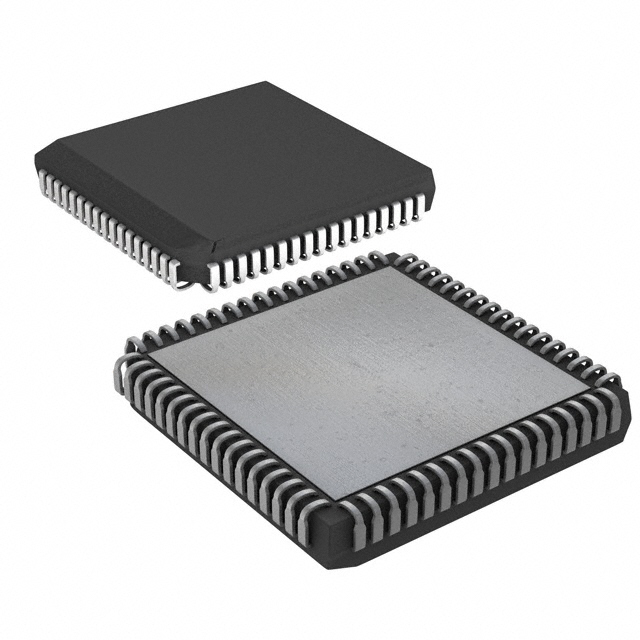
Available in 64-Pin LQFP, 68-Pin PLCC
Agricultural Equipment
Gaming Equipment
Heating, Ventilation, and
Air Conditioning
PART
DS80C390-QCR
DS80C390-QCR+
DS80C390-QNR
DS80C390-QNR+
DS80C390-FCR
DS80C390-FCR+
DS80C390-FNR
DS80C390-FNR+
TEMP RANGE
0°C to +70°C
0°C to +70°C
-40°C to +85°C
-40°C to +85°C
0°C to +70°C
0°C to +70°C
-40°C to +85°C
-40°C to +85°C
PIN-PACKAGE
68 PLCC
68 PLCC
68 PLCC
68 PLCC
64 LQFP
64 LQFP
64 LQFP
64 LQFP
+Denotes a lead(Pb)-free/RoHS-compliant device.
PIN CONFIGURATIONS
9
1
48
61
33
TOP VIEW
10
60
49
32
Dallas Semiconductor
Dallas Semiconductor
DS80C390
DS80C390
26
44
27
43
17
64
1
PLCC
16
LQFP
Note: Some revisions of this device may incorporate deviations from published specifications known as errata. Multiple revisions of any device
may be simultaneously available through various sales channels. For information about device errata, click here: www.maxim-ic.com/errata.
1 of 52
REV: 050115
�DS80C390 Dual CAN High-Speed Microprocessor
ABSOLUTE MAXIMUM RATINGS
Voltage Range on Any Pin Relative to Ground……………………………………………………….-0.3V to (VCC + 0.5V)
Voltage Range on VCC Relative to Ground……………………………………………………………………-0.3V to +6.0V
Operating Temperature Range………………………………………………………………………………..-40°C to +85°C
Storage Temperature Range………………………………………………………………………………...-55°C to +125°C
Soldering Temperature…..……………………………………………………………………..See IPC/JEDEC J-STD-020
Stresses beyond those listed under “Absolute Maximum Ratings” may cause permanent damage to the device. These are stress ratings only,
and functional operation of the device at these or any other conditions beyond those indicated in the operational sections of the specifications is
not implied. Exposure to the absolute maximum rating conditions for extended periods may affect device reliability.
DC ELECTRICAL CHARACTERISTICS (Note 10)
SYMBOL
MIN
TYP
MAX
UNITS
Supply Voltage
Power-Fail Warning
Minimum Operating Voltage
Supply Current, Active Mode (Note 1)
Supply Current, Idle Mode (Note 2)
Supply Current, Stop Mode (Note 3)
Supply Current, Stop Mode, Bandgap Enabled (Note 3)
Input Low Level
Input High Level
Input High Level for XTAL1, RST
Output Low Voltage for Port 1, 3, 4, 5 at IOL = 1.6mA
Output Low Voltage for Port 0, 1, 2, 4, 5, RD, WR, RSTOL, PSEN,
and ALE at IOL = 3.2mA (Note 5)
PARAMETER
VCC
VPFW
VRST
ICC
IIDLE
ISTOP
ISPBG
VIL
VIH
VIH2
VOL1
VRST
4.10
3.85
5.0
4.38
4.13
80
40
1
150
5.5
4.60
4.35
150
75
120
350
+0.8
VCC +0.5
VCC +0.5
0.45
V
V
V
mA
mA
µA
µA
V
V
V
V
0.45
V
Output High Voltage for Port 1, 3, 4, 5 at IOH = -50µA (Note 4)
Output High Voltage for Port 1, 3, 4, 5 at IOH = -1.5mA (Note 6)
VOH1
VOH2
2.4
2.4
V
V
Output High Voltage for Port 0, 1, 2, 4, 5, RD, WR, RSTOL, PSEN,
and ALE at IOH = -8mA (Note 5, 7)
VOH3
2.4
V
Input Low Current for Port 1, 3, 4, 5 at 0.45V (Note 8)
Logic 1 to 0 Transition Current for Port 1, 3, 4, 5 (Note 9)
Input Leakage Current for Port 0 (Input Mode Only)
RST Pulldown Resistance
IIL
IT1
IL
RRST
Note 1:
Note 2:
Note 3:
Note 4:
Note 5:
Note 6:
Note 7:
Note 8:
Note 9:
Note 10:
-0.5
2.0
0.7 x VCC
VOL2
-300
50
-55
-650
+300
170
µA
µA
µA
kΩ
Active current measured with 40MHz clock source on XTAL1, VCC = RST = 5.5V, all other pins disconnected.
Idle mode current measured with 40MHz clock source on XTAL1, VCC= 5.5V, RST = EA = VSS, all other pins disconnected.
Stop mode current measured with XTAL1 = RST = EA = VSS, VCC = 5.5V, all other pins disconnected.
RST = VCC. This condition mimics operation of pins in I/O mode.
Applies to port pins when they are used to address external memory or as CAN interface signals.
This measurement reflects the port during a 0-to-1 transition in I/O mode. During this period a one-shot circuit drives the ports hard
for two clock cycles. If a port 4 or 5 pin is functioning in memory mode with pin state of 0 and the SFR bit contains a 1, changing
the pin to an I/O mode (by writing to P4CNT) will not enable the 2-cycle strong pullup. During Stop or Idle mode the pins switch to
I/O mode, and so port 2 and port 1 (in nonmultiplexed mode) will not exhibit the 2-cycle strong pullup when entering Stop or Idle
mode.
Port 3 pins 3.6 and 3.7 have a stronger than normal pullup drive for one oscillator period following the transition of either the RD or
WR from a 0-to-1 transition.
This is the current required from an external circuit to hold a logic low level on an I/O pin while the corresponding port latch bit is
set to 1. This is only the current required to hold the low level; transitions from 1 to 0 on an I/O pin also have to overcome the
transition current.
Ports 1(in I/O mode), 3, 4, and 5 source transition current when being pulled down externally. It reaches its maximum at
approximately 2V.
Specifications to -40°C are guaranteed by design and not production tested.
2 of 52
�DS80C390 Dual CAN High-Speed Microprocessor
AC ELECTRICAL CHARACTERISTICS—(MULTIPLEXED ADDRESS/DATA BUS)
(Note 10, Note 11)
PARAMETER
Oscillator Frequency
SYMBOL
CONDITIONS
1 / tCLCL
External oscillator
External crystal
40MHz
MIN MAX
0
40
1
40
VARIABLE CLOCK
MIN
MAX
0
40
1
40
0.375 tMCS
-5
UNITS
MHz
ALE Pulse Width
tLHLL
Port 0 Instruction Address or CE0---4
Valid to ALE Low
tAVLL
0.125 tMCS - 5
ns
Address Hold After ALE Low
tLLAX1
0.125 tMCS - 5
ns
ALE Low to Valid Instruction In
tLLIV
ALE Low to PSEN Low
tLLPL
0.125 tMCS - 5
ns
PSEN Pulse Width
tPLPH
0.5 tMCS - 8
ns
PSEN Low to Valid Instruction In
tPLIV
Input Instruction Hold After PSEN
tPXIX
Input Instruction Float After PSEN
tPXIZ
0.25 tMCS - 5
ns
Port 0 Address to Valid Instruction In
tAVIV1
0.75 tMCS - 22
ns
Port 2, 4 Address to Valid Instruction
In
tAVIV2
0.875 tMCS - 30
ns
PSEN Low to Address Float
tPLAZ
0
ns
Note 11:
0.625 tMCS - 20
ns
0.5 tMCS - 20
0
0
0
ns
ns
ns
All parameters apply to both commercial and industrial temperature operation unless otherwise noted. The value tMCS is a function
of the machine cycle clock in terms of the processor’s input clock frequency. These relationships are described in the Stretch Value
Timing table. All signals characterized with load capacitance of 80pF except Port 0, ALE, PSEN, RD, and WR with 100pF.
Interfacing to memory devices with float times (turn off times) over 25ns can cause bus contention. This does not damage the
parts, but causes an increase in operating current. Specifications assume a 50% duty cycle for the oscillator. Port 2 and ALE timing
changes in relation to duty cycle variation. Some AC timing characteristic drawings contain references to the CLK signal. This
waveform is provided to assist in determining the relative occurrence of events and cannot be used to determine the timing of
signals relative to the external clock. AC timing is characterized and guaranteed by design but is not production tested.
3 of 52
�DS80C390 Dual CAN High-Speed Microprocessor
AC SYMBOLS
The DS80C390 uses timing parameters and symbols similar to the original 8051 family. The following list of timing
symbols is provided as an aid to understanding the timing diagrams.
SYMBOL
t
A
C
CE
D
H
L
I
P
Q
R
V
W
X
Z
FUNCTION
Time
Address
Clock
Chip Enable
Input Data
Logic Level High
Logic Level Low
Instruction
PSEN
Output Data
RD Signal
Valid
WR Signal
No longer a valid logic level.
Tri-State
Figure 1. Multiplexed External Program Memory Read Cycle
4 of 52
�DS80C390 Dual CAN High-Speed Microprocessor
MOVX CHARACTERISTICS (MULTIPLEXED ADDRESS/DATA BUS) (Note 12)
PARAMETER
SYMBOL
MIN
MAX
UNITS
0.5 tMCS - 20
CST x tMCS - 25
ns
ns
ns
ns
ns
ns
ns
ns
ns
ns
ns
ns
ns
ns
ns
0.375 tMCS - 5
0.5 tMCS - 5
1.5 tMCS - 10
0.125 tMCS - 5
0.25tMCS - 5
1.25 tMCS - 10
0.25tMCS-5
0.125 tMCS - 5
1.25 tMCS - 5
0.5 tMCS - 6
CST x tMCS - 10
0.5 tMCS - 6
CST x tMCS - 10
STRETCH
VALUES
CST (MD2:0)
CST = 0
1 ≤ CST ≤ 3
4 ≤ CST ≤ 7
CST = 0
1≤ CST ≤ 3
4 ≤ CST ≤ 7
CST = 0
1≤ CST ≤ 3
4 ≤ CST ≤ 7
CST = 0
1 ≤ CST ≤ 7
CST = 0
1 ≤ CST ≤ 7
CST = 0
1 ≤ CST ≤ 7
MOVX ALE Pulse Width
tLHLL2
Port 0 MOVX Address, CE0---4,
PCE0---4 Valid to ALE Low
tAVLL2
Address Hold After MOVX
Read/Write
tLLAX2
tLLAX3
RD Pulse Width
tRLRH
WR Pulse Width
tWLWH
RD Low to Valid Data In
tRLDV
Data Hold After Read
tRHDX
Data Float After Read
tRHDZ
ALE Low to Valid Data In
tLLDV
Port 0 Address, Port 4 CE, Port 5
PCE to Valid Data In
tAVDV1
Port 2, 4 Address to Valid Data In
tAVDV2
ALE Low to RD or WR Low
tLLWL
Port 0 Address, Port 4 CE, Port 5
PCE to RD or WR Low
tAVWL1
Port 2, 4 Address to or WR Low
tAVWL2
Data Valid to WR Transition
tQVWX
-8
ns
Data Hold After WR High
tWHQX
0.25 tMCS - 8
0.5tMCS - 10
1.5 tMCS - 10
ns
ns
ns
CST = 0
1 ≤ CST ≤ 3
4 ≤ CST ≤ 7
RD Low to Address Float
tRLAZ
ns
ns
ns
CST = 0
1 ≤ CST ≤ 3
4 ≤ CST ≤ 7
RD or WR High to ALE, Port 4 CE
or Port 5 PCE High
Note 12:
tWHLH
0
0.125 tMCS - 5
0.25tMCS - 5
1.25 tMCS - 5
0.25 tMCS - 11
0.5tMCS - 11
2.5 tMCS - 11
0.375 tMCS - 11
0.625tMCS - 11
2.625 tMCS - 11
ns
0.25 tMCS - 5
0.5tMCS - 5
1.5 tMCS - 5
0.625 tMCS - 20
(CST + 0.25) x tMCS - 20
(CST + 1.25) x tMCS - 20
0.75 tMCS - 26
(4CST + 0.5) x tMCS - 30
(4CST + 2.5) x tMCS - 30
0.75 tMCS - 30
(4CST + 0.5) x tMCS - 30
(4CST + 2.5) x tMCS - 30
0.125 tMCS + 10
0.25tMCS + 10
1.25 tMCS + 10
ns
ns
ns
ns
ns
ns
ns
ns
ns
ns
ns
ns
ns
ns
ns
ns
ns
ns
ns
ns
ns
CST = 0
1 ≤ CST ≤ 3
4 ≤ CST ≤ 7
CST = 0
1 ≤ CST ≤ 3
4 ≤ CST ≤ 7
CST = 0
1≤ CST ≤ 3
4 ≤ CST ≤ 7
CST = 0
1 ≤ CST ≤ 3
4 ≤ CST ≤ 7
CST =0
1 ≤ CST ≤ 3
4 ≤ CST ≤ 7
CST = 0
1 ≤ CST ≤ 3
4 ≤ CST ≤ 7
CST = 0
1 ≤ CST ≤ 3
4 ≤ CST ≤ 7
See Note 12
-5
0.25 tMCS - 7
1.25 tMCS - 7
+10
0.25 tMCS + 5
1.25 tMCS +10
All parameters apply to both commercial and industrial temperature operation. CST is the stretch cycle value determined by the
MD2:0 bits. tMCS is a time period shown in the tMCS Time Periods table. All signals characterized with load capacitance of 80pF
except Port 0, ALE, PSEN, RD, and WR with 100pF. Interfacing to memory devices with float times over 25ns can cause bus
contention and an increase in operating current. Specifications assume a 50% duty cycle for the oscillator; port 2 and ALE timing
changes in relation to duty cycle variation. Some AC timing characteristic drawings show the CLK signal, provided to determine the
relative occurrence of events and not the timing of signals relative to the external clock. During the external addressing mode, weak
latches maintain the previously driven value from the processor on Port 0 until Port 0 is overdriven by external memory; and on Port
1, 2 and 4 for one XTAL1 cycle prior to change in output address from Port 1, 2, and 4.
5 of 52
�DS80C390 Dual CAN High-Speed Microprocessor
Figure 2. Multiplexed 9-Cycle Address/Data CE0-3 MOVX Read/Write Operation
6 of 52
�DS80C390 Dual CAN High-Speed Microprocessor
Figure 3. Multiplexed 9-Cycle Address/Data PCE0-3 MOVX Read/Write Operation
7 of 52
�DS80C390 Dual CAN High-Speed Microprocessor
Figure 4. Multiplexed 2-Cycle Data Memory PCE0-3 Read or Write
Figure 5. Multiplexed 2-Cycle Data Memory CE0-3 Read
8 of 52
�DS80C390 Dual CAN High-Speed Microprocessor
Figure 6. Multiplexed 2-Cycle Data Memory CE0-3 Write
Figure 7. Multiplexed 3-Cycle Data Memory PCE0-3 Read or Write
9 of 52
�DS80C390 Dual CAN High-Speed Microprocessor
Figure 8. Multiplexed 3-Cycle Data Memory CE0-3 Read
Figure 9. Multiplexed 3-Cycle Data Memory CE0-3 Write
10 of 52
�DS80C390 Dual CAN High-Speed Microprocessor
Figure 10. Multiplexed 9-Cycle Data Memory PEC0-3 Read or Write
Figure 11. Multiplexed 9-Cycle Data Memory CE0-3 Read
11 of 52
�DS80C390 Dual CAN High-Speed Microprocessor
Figure 12. Multiplexed 9-Cycle Data Memory CE0-3 Write
12 of 52
�DS80C390 Dual CAN High-Speed Microprocessor
ELECTRICAL CHARACTERISTICS—(NONMULTIPLEXED ADDRESS/DATA BUS)
(Note 13)
PARAMETER
Oscillator Frequency
SYMBOL
1 / tCLCL
CONDITIONS
External oscillator
External crystal
40MHz
MIN MAX
0
40
1
40
VARIABLE CLOCK
MIN
MAX
0
40
1
40
UNITS
MHz
PSEN Pulse Width
tPLPH
PSEN Low to Valid Instruction In
tPLIV
Input Instruction Hold After PSEN
tPXIX
Input Instruction Float After PSEN
tPXIZ
See MOVX
Characteristics
ns
tAVIV1
0.75 tMCS - 22
ns
tAVIV2
0.875 tMCS - 30
ns
Port 1 Address, Port 4 CE to Valid
Instruction In
Port 2, 4 Address to Valid Instruction
In
Note 13:
0.5 tMCS - 8
ns
0.5 tMCS - 20
0
0
ns
ns
All parameters apply to both commercial and industrial temperature operation unless otherwise noted. The value tMCS is a function of
the machine cycle clock in terms of the processor’s input clock frequency. These relationships are described in the Stretch Value
Timing table. All signals characterized with load capacitance of 80pF except Port 0, ALE, PSEN, RD, and WR with 100pF. Interfacing
to memory devices with float times (turn off times) over 25ns can cause bus contention. This does not damage the parts, but causes
an increase in operating current. Specifications assume a 50% duty cycle for the oscillator. Port 2 and ALE timing changes in relation
to duty cycle variation. Some AC timing characteristic drawings contain references to the CLK signal. This waveform is provided to
assist in determining the relative occurrence of events and cannot be used to determine the timing of signals relative to the external
clock.
Figure 13. Nonmultiplexed External Program Memory Read Cycle
13 of 52
�DS80C390 Dual CAN High-Speed Microprocessor
MOVX CHARACTERISTICS (NONMULTIPLEXED ADDRESS/DATA BUS)
PARAMETER
SYMBOL
RD Pulse Width
tRLRH
WR Pulse Width
tWLWH
RD Low to Valid Data In
tRLDV
Data Hold After Read
tRHDX
Data Float After Read
tRHDZ
Port 1 Address, Port 4 CE, Port 5
PCE to Valid Data In
tAVDV1
Port 2, 4 Address to Valid Data In
tAVDV2
Port 0 Address, Port 4 CE, Port 5
PCE to RD or WR Low
tAVWL1
Port 2, 4 Address to RD or WR Low
tAVWL2
Data Valid to WR Transition
tQVWX
Data Hold After WR High
tWHQX
RD or WR High to ALE, Port 4 CE or
Port 5 PCE High
tWHLH
MIN
MAX
0.5 tMCS - 6
CST x tMCS - 6
0.5 tMCS - 6
CST x tMCS - 6
ns
ns
0.5 tMCS - 20
CST x tMCS - 25
0
0.25 tMCS - 11
0.5 tMCS - 11
2.5 tMCS - 11
0.375 tMCS - 11
0.625tMCS - 11
2.625 tMCS - 11
ns
ns
ns
ns
ns
-8
14 of 52
ns
STRETCH
VALUES
CST (MD2:0)
CST = 0
1 ≤ CST ≤ 7
CST = 0
1 ≤ CST ≤ 7
CST = 0
1 ≤ CST ≤ 7
ns
0.125 tMCS - 5
0.375tMCS - 5
1.375 tMCS - 5
0.75 tMCS - 26
(4CST + 0.5) x tMCS - 30
(4CST + 2.5) x tMCS - 30
0.75 tMCS - 30
(4CST + 0.625) x tMCS - 30
(4CST + 2.625) x tMCS - 30
0.25 tMCS - 8
0.5tMCS - 10
1.5 tMCS - 10
-5
0.25 tMCS - 7
1.25 tMCS - 7
UNITS
CST = 0
1 ≤ CST ≤ 3
4 ≤ CST ≤ 7
CST = 0
1 ≤ CST ≤ 3
4 ≤ CST ≤ 7
CST = 0
1 ≤ CST ≤ 3
4 ≤ CST ≤ 7
CST = 0
1 ≤ CST ≤ 3
4 ≤ CST ≤ 7
CST = 0
1 ≤ CST ≤ 3
4 ≤ CST ≤ 7
ns
ns
10
0.25 tMCS + 10
1.25 tMCS + 10
ns
CST = 0
1 ≤ CST ≤ 3
4 ≤ CST ≤ 7
CST = 0
1 ≤ CST ≤ 3
4 ≤ CST ≤ 7
�DS80C390 Dual CAN High-Speed Microprocessor
Figure 14. Nonmultiplexed 9-Cycle Address/Data CE0-3 MOVX Read/Write Operation
15 of 52
�DS80C390 Dual CAN High-Speed Microprocessor
Figure 15. Nonmultiplexed 9-Cycle Address/Data PCE0-3 MOVX Read/Write Operation
16 of 52
�DS80C390 Dual CAN High-Speed Microprocessor
Figure 16. Nonmultiplexed 2-Cycle Data Memory PCE0 - 3 Read or Write
Figure 17. Nonmultiplexed 2-Cycle Data Memory CE0-3 Read
17 of 52
�DS80C390 Dual CAN High-Speed Microprocessor
Figure 18. Nonmultiplexed 2-Cycle Data Memory CE0-3 Write
Figure 19. Nonmultiplexed 3-Cycle Data Memory PEC0-3 Read or Write
18 of 52
�DS80C390 Dual CAN High-Speed Microprocessor
Figure 20. Nonmultiplexed 3-Cycle Data Memory CE0-3 Read
Figure 21. Nonmultiplexed 3-Cycle Data Memory CE0-3 Write
19 of 52
�DS80C390 Dual CAN High-Speed Microprocessor
Figure 22. Nonmultiplexed 9-Cycle Data Memory PCE0-3 Read or Write
Figure 23. Nonmultiplexed 9-Cycle Data Memory CE0-3 Read
20 of 52
�DS80C390 Dual CAN High-Speed Microprocessor
Figure 24. Nonmultiplexed 9-Cycle Data Memory CE0-3 Write
tMCS TIME PERIODS
SYSTEM CLOCK SELECTION
4X/2X
CD1
CD0
1
0
X
X
0
0
1
1
0
0
0
1
tMCS
1 tCLCL
2 tCLCL
4 tCLCL
1024 tCLCL
EXTERNAL CLOCK CHARACTERISTICS
PARAMETER
Clock High Time
Clock Low Time
Clock Rise Time
Clock Fall Time
SYMBOL
tCHCX
tCLCX
tCLCH
tCHCL
MIN
8
8
MAX
4
4
Figure 25. External Clock Drive
21 of 52
UNITS
ns
ns
ns
ns
�DS80C390 Dual CAN High-Speed Microprocessor
SERIAL PORT MODE 0 TIMING CHARACTERISTICS
PARAMETER
SYMBOL
Serial Port Clock Cycle Time
tXLXL
Output Data Setup to Clock Rising
tQVXH
Output Data Hold from Clock Rising
tXHQX
Input Data Hold After Clock Rising
tXHDX
Clock Rising Edge to Input Data Valid
tXHDV
CONDITIONS
SM2 = 0:2 clocks per cycle
SM2 = 1:4 clocks per cycle
SM2 = 0:12 clocks per cycle
SM2 = 1:4 clocks per cycle
M2 = 0:12 clocks per cycle
SM2 = 1:4 clocks per cycle
SM2 = 0:12 clocks per cycle
SM2 = 1:4 clocks per cycle
SM2 = 0:12 clocks per cycle
SM2 = 1:4 clocks per cycle
22 of 52
TYP
12 tCLCL
4 tCLCL
10 tCLCL
3 tCLCL
2 tCLCL
tCLCL
tCLCL
0
11 tCLCL
2 tCLCL
UNITS
ns
ns
ns
ns
ns
�DS80C390 Dual CAN High-Speed Microprocessor
Figure 26. Serial Port 0 (Synchronous Mode)
HIGH-SPEED OPERATION, TXD CLK = XTAL/4 (SM2 = 1)
TRADITIONAL 8051 OPERATION, TXD CLOCK = XTAL/12 (SM2 = 0)
23 of 52
�DS80C390 Dual CAN High-Speed Microprocessor
POWER-CYCLE TIMING CHARACTERISTICS
PARAMETER
SYMBOL
TYP
Crystal Startup Time (Note 14)
tCSU
1.8
Power-On Reset Delay (Note 15)
tPOR
MAX
UNITS
ms
65,536
tCLCL
Note 14: Startup time for crystals varies with load capacitance and manufacturer. Time shown is for an 11.0592MHz crystal manufactured by
Fox Electronics.
Note 15: Reset delay is a synchronous counter of crystal oscillations during crystal startup. Counting begins when the level on the XTAL1 input
meets the VIH2 criteria. At 40MHz, this time is approximately 1.64ms.
Figure 27. Power-Cycle Timing
24 of 52
�DS80C390 Dual CAN High-Speed Microprocessor
PIN DESCRIPTION
PIN
LQFP
8, 22, 40,
56
9, 25, 41,
57
PLCC
17, 32, 51,
68
1, 18, 35,
52
NAME
VCC
GND
46
57
ALE
45
56
PSEN
47
58
EA
26
36
MUX
2
11
RST
3
12
RSTOL
23
33
XTAL2
24
34
XTAL1
55
54
53
52
51
50
49
48
67
66
65
64
63
62
61
59
AD0/D0
AD1/D1
AD2/D2
AD3/D3
AD4/D4
AD5/D5
AD6/D6
AD7/D7
FUNCTION
+5V
Digital Circuit Ground
Address Latch Enable, Output. When the MUX pin is low, this pin
outputs a clock to latch the external address LSB from the
multiplexed address/data bus on Port 0. This signal is commonly
connected to the latch enable of an external transparent latch. ALE
has a pulse width of 1.5 XTAL1 cycles and a period of four XTAL1
cycles. When the MUX pin is high, the pin will toggle continuously if
the ALEOFF bit is cleared. ALE is forced high when the device is in a
reset condition or if the ALEOFF bit is set while the MUX pin is high.
Program Store Enable, Output. This signal is the chip enable for
external ROM memory. PSEN provides an active-low pulse and is
driven high when external ROM is not being accessed.
External Access Enable, Input. This pin must be wired to GND for
proper operation.
Multiplex/Demultiplex Select, Input. This pin selects if the
address/data bus operates in multiplexed (MUX = 0) or demultiplexed
(MUX = 1) mode.
Reset, Input. The RST input pin contains a Schmitt voltage input to
recognize external active-high reset inputs. The pin also employs an
internal pulldown resistor to allow for a combination of wired-OR
external reset sources. An RC circuit is not required for power-up, as
the device provides this function internally.
Reset Output Low, Output. This active-low signal is asserted:
When the processor has entered reset through the RST pin,
During crystal warmup period following power-on or stop mode,
During a watchdog timer reset (2 cycles duration),
During an oscillator failure (if OFDE = 1),
Whenever VCC ≤ VRST.
XTAL1, XTAL2. Crystal oscillator pins support fundamental mode,
parallel resonant, and AT-cut crystals. XTAL1 is the input if an
external clock source is used in place of a crystal. XTAL2 is the
output of the crystal amplifier.
AD0–7 (Port 0), I/O. When the MUX pin is wired low, Port 0 is the
multiplexed address/data bus. While ALE is high, the LSB of a
memory address is presented. While ALE falls, the port transitions to
a bidirectional data bus. When the MUX pin is wired high, Port 0
functions as the bidirectional data bus. Port 0 cannot be modified by
software. The reset condition of Port 0 pins is high. No pullup
resistors are needed.
25 of 52
�DS80C390 Dual CAN High-Speed Microprocessor
PIN DESCRIPTION (continued)
PIN
LQFP
58–64, 1
PLCC
2–8, 10
NAME
FUNCTION
P1.0–P1.7
Port 1, I/O. Port 1 can function as an 8-bit bidirectional I/O port, the
nonmultiplexed A0–A7 signals (when the MUX pin = 1), and as an
alternate interface for internal resources. Setting the SP1EC bit
relocates RXD1 and TXD1 to Port 5. The reset condition of Port 1 is
all bits at logic 1 through a weak pullup. The logic 1 state also serves
as an input mode, since external circuits writing to the port can
overdrive the weak pullup. When software clears any port pin to 0, a
strong pulldown is activated that remains on until either a 1 is written
to the port pin or a reset occurs. Writing a 1 after the port has been at
0 activates a strong transition driver, followed by a weaker sustaining
pullup. Once the momentary strong driver turns off, the port once
again becomes the output (and input) high state.
Port
Alternate Function
58
2
A0
P1.0
T2 External I/O for Timer/Counter 2
59
3
A1
P1.1
T2EX Timer/Counter 2 Capture/Reload Trigger
60
4
A2
P1.2
RXD1 Serial Port 1 Input
61
5
A3
P1.3
TXD1 Serial Port 1 Output
62
6
A4
P1.4
INT2 External Interrupt 2 (Positive Edge Detect)
63
7
A5
P1.5
64
8
A6
P1.6
INT3 External Interrupt 3 (Negative Edge Detect)
INT4 External Interrupt 4 (Positive Edge Detect)
1
35
36
37
38
39
42
43
44
10
46
47
48
49
50
53
54
55
A7
A8 (P2.0)
A9 (P2.1)
A10 (P2.2)
A11 (P2.3)
A12 (P2.4)
A13 (P2.5)
A14 (P2.6)
A15 (P2.7)
P1.7
INT5 External Interrupt 5 (Negative Edge Detect)
4–7,
10–13
13–16,
19–22
4
5
6
7
10
11
12
13
13
14
15
16
19
20
21
22
P3.0–P3.7
A15–A8 (Port 2), Output. Port 2 serves as the MSB for external
addressing. The port automatically asserts the address MSB during
external ROM and RAM access. Although the Port 2 SFR exists, the
SFR value never appears on the pins (due to memory access).
Therefore, accessing the Port 2 SFR is only useful for MOVX A, @Ri
or MOVX @Ri, A instructions, which use the Port 2 SFR as the
external address MSB.
Port 3, I/O. Port 3 functions as an 8-bit bidirectional I/O port and as an
alternate interface for several resources found on the traditional 8051.
The reset condition of Port 1 is all bits at logic 1 through a weak pullup.
The logic 1 state also serves as an input mode, since external circuits
writing to the port can overdrive the weak pullup. When software clears
any port pin to 0, the device activates a strong pulldown that remains on
until either a 1 is written to the port pin or a reset occurs. Writing a 1 after
the port has been at 0 activates a strong transition driver, followed by a
weaker sustaining pullup. Once the momentary strong driver turns off,
the port once again becomes the output (and input) high state.
Port
P3.0
P3.1
P3.2
P3.3
P3.4
P3.5
P3.6
P3.7
Alternate Function
RXD0 Serial Port 0 Input
TXD0 Serial Port 0 Output
INT0 External Interrupt 0
INT1 External Interrupt 1
T0 Timer 0 External Input
T1/XCLK Timer 1 External Input/External Clock Output
WR External Data Memory Write Strobe
RD External Data Memory Read Strobe
26 of 52
�DS80C390 Dual CAN High-Speed Microprocessor
PIN DESCRIPTION (continued)
PIN
LQFP
PLCC
34–27
45, 44,
42–37
34
33
32
31
30
29
28
27
45
44
42
41
40
39
38
37
21–14
31–27,
25–23
21
20
19
18
17
16
15
14
31
30
29
28
27
25
24
23
9, 26, 43,
60
NAME
FUNCTION
P4.0–P4.7
Port 4, I/O. Port 4 can function as an 8-bit, bidirectional I/O port, and
as the source for external address and chip enable signals for
program and data memory. Port pins are configured as I/O or
memory signals via the P4CNT register. The reset condition of Port 1
is all bits at logic 1 via a weak pullup. The logic 1 state also serves as
an input mode, since external circuits writing to the port can overdrive
the weak pullup. When software clears any port pin to 0, the device
activates a strong pulldown that remains on until either a 1 is written
to the port pin or a reset occurs. Writing a 1 after the port has been at
0 will activate a strong transition driver, followed by a weaker
sustaining pullup. Once the momentary strong driver turns off, the
port once again becomes the output (and input) high state.
P5.0–P5.7
N.C.
Port
Alternate Function
P4.0
CE0 Program Memory Chip Enable 0
P4.1
CE1 Program Memory Chip Enable 1
P4.2
CE2 Program Memory Chip Enable 2
P4.3
CE3 Program Memory Chip Enable 3
P4.4
A16 Program/Data Memory Address 16
P4.5
A17 Program/Data Memory Address 17
P4.6
A18 Program/Data Memory Address 18
P4.7
A19 Program/Data Memory Address 19
Port 5, I/O. Port 5 can function as an 8-bit, bidirectional I/O port, the
CAN interface, or as peripheral enable signals. Setting the SP1EC bit
will relocate the RXD1 and TXD1 functions to P5.3-P5.2 as described
in the High-Speed Microcontroller User’s Guide: DS80C390
Supplement. The reset condition of Port 1 is all bits at logic 1 via a
weak pullup. The logic 1 state also serves as an input mode, since
external circuits writing to the port can overdrive the weak pullup.
When software clears any port pin to 0, the device activates a strong
pulldown that remains on until either a 1 is written to the port pin or a
reset occurs. Writing a 1 after the port has been at 0 will activate a
strong transition driver, followed by a weaker sustaining pullup. Once
the momentary strong driver turns off, the port once again becomes
the output (and input) high state.
Port
Alternate Function
P5.0
C0TX CAN0 Transmit Output
P5.1
C0RX CAN0 Receive Input
P5.2
C1RX CAN1 Receive Input (optional RXD1)
P5.3
C1TX CAN1 Transmit Output (optional TXD1)
P5.4
PCE0 Peripheral Chip Enable 0
P5.5
PCE1 Peripheral Chip Enable 1
P5.6
PCE2 Peripheral Chip Enable 2
P5.7
PCE3 Peripheral Chip Enable 3
Not Connected. Reserved. These pins are reserved for use with
future devices in this family and should not be connected.
27 of 52
�DS80C390 Dual CAN High-Speed Microprocessor
Figure 28. Block Diagram
DS80C390
28 of 52
�DS80C390 Dual CAN High-Speed Microprocessor
FEATURES
80C52 Compatible
8051-Instruction-Set Compatible
Four 8-Bit I/O Ports
Three 16-Bit Timer/Counters
256 Bytes Scratchpad RAM
High-Speed Architecture
4 Clocks/Machine Cycle (8051 = 12)
Runs DC to 40MHz Clock Rates
Frequency Multiplier Reduces Electromagnetic
Interference (EMI)
Single-Cycle Instruction in 100ns
16/32-Bit Math Coprocessor
4kB Internal SRAM Usable as
Program/Data/Stack Memory
Enhanced Memory Architecture
Addresses Up to 4MB External
Defaults to True 8051-Memory Compatibility
User-Enabled 22-Bit Program/Data Counter
16-Bit/22-Bit Paged/22-Bit Contiguous Modes
User-Selectable Multiplexed/Nonmultiplexed
Memory Interface
Optional 10-Bit Stack Pointer
Two Full-Function CAN 2.0B Controllers
15 Message Centers Per Controller
Standard 11-Bit or Extended 29-Bit Identification
Modes
Supports DeviceNet™, SDS, and Higher Layer
CAN Protocols
Disables Transmitter During Autobaud
SIESTA Low-Power Mode
Two Full-Duplex Hardware Serial Ports
Programmable IrDA Clock
High-Integration Controller Includes:
Power-Fail Reset
Early-Warning Power-Fail Interrupt
Programmable Watchdog Timer
Oscillator-Fail Detection
16 Interrupt Sources with Six External
Available in 64-Pin LQFP and 68-Pin PLCC
DETAILED DESCRIPTION
The DS80C390 features two full-function controller area network (CAN) 2.0B controllers. Status and control
registers are distributed between SFRs and 512 bytes of internal MOVX memory for maximum flexibility. In addition
to standard 11-bit or 29-extended message identifiers, the device supports two separate 8-bit media masks and
media arbitration fields to support the use of higher-level CAN protocols such as DeviceNet and SDS.
All of the standard 8051 resources such as three timer/counters, serial port, and four 8-bit I/O ports (plus two 8-bit
ports dedicated to memory interfacing) are included in the DS80C390. In addition it includes a second hardware
serial port, seven additional interrupts, programmable watchdog timer, brownout monitor, power-fail reset, and a
programmable output clock that supports an IrDA interface. The device provides dual data pointers with
increment/decrement features to speed block data memory moves. It also can adjust the speed of MOVX data
memory access from 2 to 12 machine cycles for flexibility in addressing external memory and peripherals.
The device incorporates a 4kB SRAM, which can be configured as various combinations of MOVX memory,
program memory, and optional stack memory. A 22-bit program counter supports access to a maximum of 4MB of
external program memory and 4MB of external data memory. A 10-bit stack pointer addresses up to 1kB of MOVX
memory for increased code efficiency.
A new power-management mode (PMM) is useful for portable or power-conscious applications. This feature allows
software to switch from the standard machine cycle rate of 4 clocks per cycle to 1024 clocks per cycle. For
example, at 12MHz standard operation has a machine cycle rate of 3MHz. In PMM at the same external clock
speed, software can select 11.7kHz machine cycle rate. There is a corresponding reduction in power consumption
when the processor runs slower.
The EMI reduction feature allows software to select a reduced electromagnetic interference (EMI) mode by
disabling the ALE signal when it is unneeded. The device also incorporates active current control on the address
and data buses, reducing EMI by minimizing transients when interfacing to external circuitry.
80C32 COMPATIBILITY
The DS80C390 is a CMOS 80C32-compatible microcontroller designed for high performance. Every effort has
been made to keep the core device familiar to 80C32 users while adding many new features.
DeviceNet is a trademark of Open DeviceNet Vendor Association, Inc.
29 of 52
�DS80C390 Dual CAN High-Speed Microprocessor
Because the device runs the standard 8051 instruction set, in general, software written for existing 80C32-based
systems will work on the DS80C390. The primary exceptions are related to timing-critical issues, since the highperformance core of the microcontroller executes instructions much faster than the original. Memory interfacing is
performed identically to the standard 80C32. The high-speed nature of the DS80C390 core slightly changes the
interface timing, and designers are advised to consult the timing diagrams in this data sheet for more information.
The DS80C390 provides the same timer/counter resources, full duplex serial port, 256 bytes of scratchpad RAM
and I/O ports as the standard 80C32. Timers default to a 12 clocks-per-machine cycle operation to keep timing
compatible with original 8051 systems, but can be programmed to run at the faster four clocks-per-machine cycle if
desired. New hardware functions are accessed using special function registers that do not overlap with standard
80C32 locations.
This data sheet provides only a summary and overview of the DS80C390. Detailed descriptions are available in the
High-Speed Microcontroller User’s Guide: DS80C390 Supplement. This data sheet assumes a familiarity with the
architecture of the standard 80C32. In addition to the basic features of that device, the DS80C390 incorporates
many new features.
PERFORMANCE OVERVIEW
The DS80C390’s higher performance comes not just from increasing the clock frequency but also from a more
efficient design. This updated core removes the dummy memory cycles that are present in a standard, 12 clocksper-machine cycle 8051. In the DS80C390, the same machine cycle takes 4 clocks. Thus the fastest instruction,
one machine cycle, executes three times faster for the same crystal frequency. The majority of instructions on the
DS80C390 see the full 3-to-1 speed improvement, while a few execute between 1.5 and 2.4 times faster.
Regardless of specific performance improvements, all instructions are faster than the original 8051.
Improvement of individual programs depends on the actual mix of instructions used. Speed-sensitive applications
should make the most use of instructions that are three times faster. However, the large number of 3-to-1 improved
op codes makes dramatic speed improvements likely for any arbitrary combination of instructions. These
architecture improvements and the submicron CMOS design produce a peak instruction cycle in 100ns (10 MIPS).
The dual data pointer feature also allows the user to eliminate wasted instructions when moving blocks of memory.
INSTRUCTION SET SUMMARY
All instructions perform exactly the same functions as their 8051 counterparts. Their effect on bits, flags, and other
status functions is identical. However, the timing of instructions is different, both in absolute and relative number of
clocks. The absolute timing of software loops can be calculated using a table in the High-Speed Microcontroller
User’s Guide: DS80C390 Supplement. However, counter/timers default to run at the traditional 12 clocks per
increment. In this way, timer-based events occur at the standard intervals with software executing at higher speed.
Timers optionally can run at the faster four clocks per increment to take advantage of faster processor operation.
The relative time of two DS80C390 instructions might differ from the traditional 8051. For example, in the original
architecture the “MOVX A, @DPTR” instruction and the “MOV direct, direct” instruction required the same amount
of time: two machine cycles or 24 oscillator cycles. In the DS80C390, the MOVX instruction takes as little as two
machine cycles, or eight oscillator cycles, but the “MOV direct, direct” uses three machine cycles, or 12 oscillator
cycles. While both are faster than their original counterparts, they now have different execution times. This is
because the device usually uses one instruction cycle for each instruction byte. Examine the timing of each
instruction for familiarity with the changes. Note that a machine cycle now requires just four clocks, and provides
one ALE pulse per cycle. Many instructions require only one cycle, but some require five. Refer to the High-Speed
Microcontroller User’s Guide: DS80C390 Supplement for details and individual instruction timing.
SPECIAL FUNCTION REGISTERS (SFRs)
Special function registers (SFRs) control most special features of the microcontroller, allowing the device to have
many new features but use the same instruction set as the 8051. When writing software to use a new feature, an
equate statement defines the SFR to an assembler or compiler. This is the only change needed to access the new
function. The DS80C390 duplicates the SFRs contained in the standard 80C52. Table 1 shows the register
addresses and bit locations. Many are standard 80C52 registers. The High-Speed Microcontroller User’s Guide:
DS80C390 Supplement contains a full description of all SFRs.
30 of 52
�DS80C390 Dual CAN High-Speed Microprocessor
Table 1. SFR Locations
REGISTER
BIT7
BIT6
BIT5
BIT4
BIT3
BIT2
BIT1
BIT0
ADDRESS
P4
SP
DPL
DPH
DPL1
DPH1
DPS
PCON
TCON
TMOD
TL0
TL1
TH0
TH1
CKCON
P1
EXIF
P4CNT
DPX
DPX1
C0RMS0
C0RMS1
SCON0
SBUF0
ESP
AP
ACON
C0TMA0
C0TMA1
P2
P5
P5CNT
C0C
C0S
C0IR
C0TE
C0RE
IE
SADDR0
SADDR1
C0M1C
C0M2C
C0M3C
C0M4C
C0M5C
P3
C0M6C
C0M7C
C0M8C
C0M9C
C0M10C
IP
SADEN0
SADEN1
C0M11C
C0M12C
C0M13C
P4.7
P4.6
P4.5
P4.4
P4.3
P4.2
P4.1
P4.0
ID1
SMOD_0
TF1
GATE
ID0
SMOD0
TR1
C/T
TSL
OFDF
TF0
M1
—
OFDE
TR0
M0
—
GF1
IE1
GATE
—
GF0
IT1
C/T
—
STOP
IE0
M1
SEL
IDLE
IT0
M0
80h
81h
82h
83h
84h
85h
86h
87h
88h
89h
8Ah
8Bh
8Ch
8Dh
8Eh
90h
91h
92h
93h
95h
96h
97h
98h
99h
9Bh
9Ch
9Dh
9Eh
9Fh
A0h
A1h
A2h
A3h
A4h
A5h
A6h
A7h
A8h
A9h
AAh
ABh
ACh
ADh
AEh
AFh
B0h
B3h
B4h
B5h
B6h
B7h
B8h
B9h
BAh
BBh
BCh
BDh
WD1
WD0
INT5/P1.7 INT4/P1.6
IE5
IE4
—
SBCAN
T2M
T1M
T0M
MD2
MD1
INT3/P1.5 INT2/P1.4 TXD1/P1.3 RXD1/P1.2 T2EX/P1.1
IE3
IE2
CKRY
RGMD
RGSL
P4CNT.5 P4CNT.4 P4CNT.3 P4CNT.2 P4CNT.1
MD0
T2/P1.0
BGS
P4CNT.0
SM0/FE_0
SM1_0
SM2_0
REN_0
TB8_0
RB8_0
TI_0
RI_0
—
—
—
—
—
—
ESP.1
ESP.0
—
—
—
—
—
SA
AM1
AM0
P2.7
P5.7
CAN1BA
ERIE
BSS
INTIN7
P2.6
P5.6
CAN0BA
STIE
EC96/128
INTIN6
P2.5
P5.5
SP1EC
PDE
WKS
INTIN5
P2.4
P5.4
C1_I/O
SIESTA
RXS
INTIN4
P2.3
P5.3
C0_I/O
CRST
TXS
INTIN3
P2.2
P5.2
P5CNT.2
AUTOB
ER2
INTIN2
P2.1
P5.1
P5CNT.1
ERCS
ER1
INTIN1
P2.0
P5.0
P5CNT.0
SWINT
ER0
INTIN0
EA
ES1
ET2
ES0
ET1
EX1
ET0
EX0
MSRDY
MSRDY
MSRDY
MSRDY
MSRDY
P3.7
MSRDY
MSRDY
MSRDY
MSRDY
MSRDY
—
ETI
ETI
ETI
ETI
ETI
P3.6
ETI
ETI
ETI
ETI
ETI
PS1
ERI
ERI
ERI
ERI
ERI
T1
ERI
ERI
ERI
ERI
ERI
PT2
INTRQ
INTRQ
INTRQ
INTRQ
INTRQ
T0
INTRQ
INTRQ
INTRQ
INTRQ
INTRQ
PS0
EXTRQ
EXTRQ
EXTRQ
EXTRQ
EXTRQ
INT1
EXTRQ
EXTRQ
EXTRQ
EXTRQ
EXTRQ
PT1
MTRQ
MTRQ
MTRQ
MTRQ
MTRQ
INT0
MTRQ
MTRQ
MTRQ
MTRQ
MTRQ
PX1
ROW/TIH
ROW/TIH
ROW/TIH
ROW/TIH
ROW/TIH
TXD0
ROW/TIH
ROW/TIH
ROW/TIH
ROW/TIH
ROW/TIH
PT0
DTUP
DTUP
DTUP
DTUP
DTUP
RXD0
DTUP
DTUP
DTUP
DTUP
DTUP
PX0
MSRDY
MSRDY
MSRDY
ETI
ETI
ETI
ERI
ERI
ERI
INTRQ
INTRQ
INTRQ
EXTRQ
EXTRQ
EXTRQ
MTRQ
MTRQ
MTRQ
ROW/TIH
ROW/TIH
ROW/TIH
DTUP
DTUP
DTUP
31 of 52
�DS80C390 Dual CAN High-Speed Microprocessor
Table 1. SFR Locations (continued)
REGISTER
BIT7
BIT6
BIT5
BIT4
BIT3
BIT2
BIT1
BIT0
ADDRESS
C0M14C
C0M15C
SCON1
SBUF1
PMR
STATUS
MCON
TA
T2CON
T2MOD
RCAP2L
RCAP2H
TL2
TH2
COR
PSW
MCNT0
MCNT1
MA
MB
MC
C1RMS0
C1RMS1
WDCON
C1TMA0
C1TMA1
ACC
C1C
C1S
C1IR
C1TE
C1RE
EIE
MXAX
C1M1C
C1M2C
C1M3C
C1M4C
C1M5C
B
C1M6C
C1M7C
C1M8C
C1M9C
C1M10C
EIP
C1M11C
C1M12C
C1M13C
C1M14C
C1M15C
MSRDY
MSRDY
SM0/FE_1
ETI
ETI
SM1_1
ERI
ERI
SM2_1
INTRQ
INTRQ
REN_1
EXTRQ
EXTRQ
TB8_1
MTRQ
MTRQ
RB8_1
ROW/TIH
ROW/TIH
TI_1
DTUP
DTUP
RI_1
CD1
PIP
IDM1
CD0
HIP
IDM0
SWB
LIP
CMA
CTM
—
—
4X/2X
SPTA1
PDCE3
ALEOFF
SPRA1
PDCE2
—
SPTA0
PDCE1
—
SPRA0
PDCE0
TF2
—
EXF2
—
RCLK
—
TCLK
D13T1
EXEN2
D13T2
TR2
—-
C/T2
T2OE
CP/RL2
DCEN
IRDACK
CY
LSHIFT
MST
C1BPR7
AC
CSE
MOF
C1BPR6
F0
SCB
—
C0BPR7
RS1
MAS4
CLM
C0BPR6
RS0
MAS3
—
COD1
OV
MAS2
—
COD0
F1
MAS1
—
CLKOE
P
MAS0
—
SMOD_1
POR
EPFI
PFI
WDIF
WTRF
EWT
RWT
ERIE
BSS
INTIN7
STIE
CECE
INTIN6
PDE
WKS
INTIN5
SIESTA
RXS
INTIN4
CRST
TXS
INTIN3
AUTOB
ER2
INTIN2
ERCS
ER1
INTIN1
SWINT
ER0
INTIN0
CANBIE
C0IE
C1IE
EWDI
EX5
EX4
EX3
EX2
MSRDY
MSRDY
MSRDY
MSRDY
MSRDY
ETI
ETI
ETI
ETI
ETI
ERI
ERI
ERI
ERI
ERI
INTRQ
INTRQ
INTRQ
INTRQ
INTRQ
EXTRQ
EXTRQ
EXTRQ
EXTRQ
EXTRQ
MTRQ
MTRQ
MTRQ
MTRQ
MTRQ
ROW/TIH
ROW/TIH
ROW/TIH
ROW/TIH
ROW/TIH
DTUP
DTUP
DTUP
DTUP
DTUP
MSRDY
MSRDY
MSRDY
MSRDY
MSRDY
CANBIP
MSRDY
MSRDY
MSRDY
MSRDY
MSRDY
ETI
ETI
ETI
ETI
ETI
C0IP
ETI
ETI
ETI
ETI
ETI
ERI
ERI
ERI
ERI
ERI
C1IP
ERI
ERI
ERI
ERI
ERI
INTRQ
INTRQ
INTRQ
INTRQ
INTRQ
PWDI
INTRQ
INTRQ
INTRQ
INTRQ
INTRQ
EXTRQ
EXTRQ
EXTRQ
EXTRQ
EXTRQ
PX5
EXTRQ
EXTRQ
EXTRQ
EXTRQ
EXTRQ
MTRQ
MTRQ
MTRQ
MTRQ
MTRQ
PX4
MTRQ
MTRQ
MTRQ
MTRQ
MTRQ
ROW/TIH
ROW/TIH
ROW/TIH
ROW/TIH
ROW/TIH
PX3
ROW/TIH
ROW/TIH
ROW/TIH
ROW/TIH
ROW/TIH
DTUP
DTUP
DTUP
DTUP
DTUP
PX2
DTUP
DTUP
DTUP
DTUP
DTUP
BEh
BFh
C0h
C1h
C4h
C5h
C6h
C7h
C8h
C9h
CAh
CBh
CCh
CDh
CEh
D0h
D1h
D2h
D3h
D4h
D5h
D6h
D7h
D8h
DEh
DFh
E0h
E3h
E4h
E5h
E6h
E7h
E8h
EAh
EBh
ECh
EDh
EEh
EFh
F0h
F3h
F4h
F5h
F6h
F7h
F8h
FBh
FCh
FDh
FEh
FFh
Note: Shaded bits are timed-access protected.
32 of 52
�DS80C390 Dual CAN High-Speed Microprocessor
ON-CHIP ARITHMETIC ACCELERATOR
An on-chip math accelerator allows the microcontroller to perform 32-bit and 16-bit multiplication, division, shifting,
and normalization using dedicated hardware. Math operations are performed by sequentially loading three special
registers. The mathematical operation is determined by the sequence in which three dedicated SFRs (MA, MB, and
MC) are accessed, eliminating the need for a special step to choose the operation. The normalize function
facilitates the conversion of 4-byte unsigned binary integers into floating point format. Table 2 shows the operations
supported by the math accelerator and their time of execution.
Table 2. Arithmetic Accelerator Execution Times
OPERATION
RESULT
32-Bit/16-Bit Divide
16-Bit/16-Bit Divide
16-Bit/16-Bit Multiply
32-Bit Shift Left/Right
32-Bit Normalize
32-Bit Quotient, 16-Bit Remainder
16-Bit Quotient, 16-Bit Remainder
32-Bit Product
32-Bit Result
32-Bit Mantissa, 5-Bit Exponent
EXECUTION TIME
(tCLCL)
36
24
24
36
36
Table 3 demonstrates the procedure to perform mathematical operations using the hardware math accelerator. The
MA and MB registers must be loaded and read in the order shown for proper operation, although accesses to any
other registers can be performed between access to the MA or MB registers. An access to the MA, MB, or MC
registers out of sequence corrupts the operation, requiring the software to clear the MST bit to restart the math
accelerator state machine. Consult the description of the MCNT0 SFR for details of how the shift and normalize
functions operate.
Software must ensure that the input value for the normalize operation is not zero or the function will not complete.
Compilers such as the one from Keil Software have updated their libraries and compensate for this condition.
Table 3. Arithmetic Accelerator Sequencing
DIVIDE (32/16 OR 16/16)
Load MA with dividend LSB.
Load MA with dividend LSB + 1.*
Load MA with dividend LSB + 2.*
Load MA with dividend MSB.
Load MB with divisor LSB.
Load MB with divisor MSB.
Poll the MST bit until cleared. (9 machine cycles).
Read MA to retrieve the quotient MSB.
Read MA to retrieve the quotient LSB + 2.**
Read MA to retrieve the quotient LSB + 1.**
Read MA to retrieve the quotient LSB.
Read MB to retrieve the remainder MSB.
Read MB to retrieve the remainder LSB.
MULTIPLY (16 X 16)
Load MB with multiplier LSB.
Load MB with multiplier MSB.
Load MA with multiplicand LSB.
Load MA with multiplicand MSB.
Poll the MST bit until cleared. (6 machine cycles).
Read MA for product MSB.
Read MA for product LSB + 2.
Read MA for product LSB + 1.
Read MA for product LSB.
SHIFT RIGHT/LEFT
Load MA with data LSB.
Load MA with data LSB + 1.
Load MA with data LSB + 2.
Load MA with data MSB.
Configure MCNT0 register as required
Poll the MST bit until cleared. (9 machine cycles)
Read MA for result MSB.
Read MA for result LSB + 2.
Read MA for result LSB + 1.
Read MA for result LSB.
NORMALIZE
Load MA with data LSB.
Load MA with data LSB + 1.
Load MA with data LSB + 2.
Load MA with data MSB.***
Load MCNT0 with 00h.
Poll the MST bit until cleared. (9 machine cycles)
Read MA for mantissa MSB.
Read MA for mantissa LSB + 2.
Read MA for mantissa LSB + 1.
Read MA for mantissa LSB.
Read MCNT0.4–MCNT0.0 for exponent.
*Not performed for 16-bit numerator.
**Not performed for 16/16 divide.
***Value to be normalized must be nonzero.
33 of 52
�DS80C390 Dual CAN High-Speed Microprocessor
40-BIT ACCUMULATOR
The accelerator also incorporates an automatic accumulator function, permitting the implementation of multiplyand-accumulate and divide-and-accumulate functions without any additional delay. Each time the accelerator is
used for a multiply or divide operation, the result is transparently added to a 40-bit accumulator. This can greatly
increase speed of DSP and other high-level math operations.
The accumulator can be accessed anytime the multiply/accumulate status flag (MCNT1;D2h) is cleared. The
accumulator is initialized by performing five writes to the multiplier C register (MC;D5h), LSB first. The 40-bit
accumulator can be read by performing five reads of the multiplier C register, MSB first.
MEMORY ADDRESSING
The DS80C390 incorporates three internal memory areas:
256 bytes of scratchpad (or direct) RAM
4kB of SRAM configurable as various combinations of MOVX data memory, stack memory, and MOVC
program memory
512 bytes of RAM reserved for the CAN message centers.
Up to 4MB of external memory is addressed via a multiplexed or demultiplexed 20-bit address bus/8-bit data bus
and four chip-enable (active during program memory access) or four peripheral-enable (active during data memory
access) signals. Three different addressing modes are supported, as selected by the AM1, AM0 bits in the ACON
SFR.
16-Bit Address Mode
Memory is accessed by 16-bit address mode similarly to the traditional 8051. It is op-code compatible with the 8051
microprocessor and identical to the byte and cycle count of the Dallas Semiconductor High-Speed Microcontroller
family. A device operating in this mode can access up to 64kB of program and data memory. The device defaults to
this mode following any reset.
22-Bit Paged-Address Mode
The 22-bit paged-address mode retains binary-code compatibility with the 8051 instruction set, but adds one
machine cycle to the ACALL, LCALL, RET, and RETI instructions with respect to Dallas Semiconductor’s HighSpeed Microcontroller family timing. This is transparent to standard 8051 compilers. Interrupt latency is also
increased by one machine cycle. In this mode, interrupt vectors are fetched from 0000xxh.
22-Bit Contiguous Address Mode
The 22-bit contiguous addressing mode uses a full 22-bit program counter, and all modified branching instructions
automatically save and restore the entire program counter. The 22-bit branching instructions such as ACALL,
AJMP, LCALL, LJMP, MOV DPTR, RET, and RETI instructions require an assembler, compiler, and linker that
specifically supports these features. The INC DPTR is lengthened by one cycle but remains byte-count-compatible
with the standard 8051 instruction set.
Internally, the device uses a 22-bit program counter. The lowest order 22 bits are used for memory addressing,
with a special 23rd bit used to map the 4kB SRAM above the 4MB memory space in bootstrap loader applications.
Address bits 16–23 for the 22-bit addressing modes are generated through additional SFRs dependent on the type
of instruction as shown in Table 4.
Table 4. Extended Address Generation
INSTRUCTION
MOVX instructions using DPTR
MOVX instructions using DPTR1
MOVX instructions using @Ri
Addressing program memory in 22-bit
paged mode
10-bit stack pointer mode
ADDRESS BITS
23–16
DPX;93h
DPX1;95h
MXAX;EAh
ADDRESS BITS
15–8
DPH;83h
DPH1;85h
P2;A0h
ADDRESS BITS
7–0
DPL;82h
DPL1;84h
Ri
AP;9Ch
—
—
—
ESP;9Bh
SP;81h
34 of 52
�DS80C390 Dual CAN High-Speed Microprocessor
INTERNAL MOVX SRAM
The DS80C390 contains 4kB of SRAM that can be configured as user accessible MOVX memory, program
memory, or optional stack memory. The specific configuration and locations are governed by the internal data
memory configuration bits (IDM1, IDM0) in the memory control register (MCON;C6h). Note that when the SA bit
(ACON.2) is set, the first 1kB of the MOVX data memory is reserved for use by the 10-bit expanded stack. Internal
memory accesses will not generate WR, RD, or PSEN strobes.
The DS80C390 can configure its 4kB of internal SRAM as combined program and data memory. This allows the
application software to execute self-modifiable code. The technique loads the 4kB SRAM with bootstrap loader
software, and then modifies the IDM1 and IDM0 bits to map the 4kB starting at memory location 40000h. This
allows the system to run the bootstrap loader without disturbing the 4MB external memory bus, making the device
in-system reprogrammable for flash or NV RAM.
Table 5. Internal MOVX SRAM Configuration
MEMORY
IDM1
0
0
0
0
1
1
1
1
IDM0
0
0
1
1
0
0
1
1
CMA
0
1
0
1
0
1
0
1
MOVX DATA
CAN MESSAGE
SHARED PROGRAM/DATA
00F000h–00FFFFh
00F000h–00FFFFh
000000h–000FFFh
000000h–000FFFh
400000h–400FFFh
400000h–400FFFh
—
—
00EE00h–00EFFFh
401000h–4011FFh
00EE00h–00EFFFh
401000h–4011FFh
00EE00h–00EFFFh
401000h–4011FFh
00EE00h–00EFFFh
401000h–4011FFh
—
—
—
—
—
—
400000h–400FFFh*
400000h–400FFFh*
*10-bit expanded stack is not available in shared program/data memory mode.
EXTERNAL MEMORY ADDRESSING
The enabling and mapping of the chip-enable signals is done through the Port 4 control register (P4CNT;92h) and
memory control register (MCON; 96h). Table 7 shows which chip-enable and address line signals are active on
Port 4. Following reset, the device will be configured with P4.7–P4.4 as address lines and P4.3–P4.0 configured as
CE3-0, with the first program fetch being performed from 00000h with CE0 active. The following tables illustrate
which memory ranges are controlled by each chip enable as a function of which address lines are enabled.
Table 6. External Memory Addressing Pin Assignments
ADDRESS/DATA
BUS
CE3---CE0
PCE3---PCE0
ADDR 19–16
ADDR 15–8
ADDR 7–0
DATA BUS
Multiplexed
P4.3–P4.0
P5.7–P5.4
P4.7–P4.4
P2
P0
P0
Demultiplexed
P4.3–P4.0
P5.7–P5.4
P4.7–P4.4
P2
P1
P0
Table 7. Extended Address and Chip-Enable Generation
P4CNT.5–3
000
100
101
110
111(default)
P4.7
I/O
I/O
I/O
I/O
A19
PORT 4 PIN FUNCTION
P4.6
P4.5
I/O
I/O
I/O
I/O
I/O
A17
A18
A17
A18
A17
P4.4
I/O
A16
A16
A16
A16
P4CNT.2–0
000
100
101
110
111(default)
35 of 52
P4.3
I/O
I/O
I/O
I/O
CE3
PORT 4 PIN FUNCTION
P4.2
P4.1
I/O
I/O
I/O
I/O
I/O
CE1
CE2
CE1
CE2
CE1
P4.0
I/O
CE0
CE0
CE0
CE0
�DS80C390 Dual CAN High-Speed Microprocessor
Table 8. Program Memory Chip-Enable Boundaries
P4CNT.5–3
CE0
CE1
CE2
CE3
000
100
101
110
111(default)
0h–7FFFh
0h–1FFFFh
0h–3FFFFh
0h–7FFFFh
0–FFFFFh
8000h–FFFFh
20000h–3FFFFh
40000h–7FFFFh
80000h–FFFFFh
100000h–1FFFFFh
10000h–17FFFh
40000h–5FFFFh
80000h–BFFFFh
100000h–17FFFFh
200000h–2FFFFFh
18000h–1FFFFh
60000h–7FFFFh
C0000h–FFFFFh
180000h–1FFFFFh
300000h–3FFFFFh
The DS80C390 incorporates a feature allowing PCE and CE signals to be combined. This is useful when
incorporating modifiable code memory as part of a bootstrap loader or for in-system reprogrammability. Setting the
PDCE3---0 (MCON.3–0) bits causes the corresponding chip-enable signal to function for both MOVC and MOVX
operations. Write access to combined program and data memory blocks is controlled by the WR signal, and read
access is controlled by the PSEN signal. This feature is especially useful if the design achieves in-system
reprogrammability via external flash memory, in which a single device is accessed through both MOVC instructions
(program fetch) and MOVX write operations (updates to code memory). In this case, the internal SRAM is placed in
the program/data configuration and loaded with a small bootstrap loader program stored in the external flash
memory. The device then executes the internal bootstrap loader routine to modify/update the program memory
located in the external flash memory.
STRETCH MEMORY CYCLES
The DS80C390 allows user-application software to select the number of machine cycles it takes to execute a
MOVX instruction, allowing access to both fast and slow off-chip data memory and/or peripherals without glue
logic. High-speed systems often include memory-mapped peripherals such as LCDs or UARTs with slow access
times, so it may not be necessary or desirable to access external devices at full speed. The microprocessor can
perform a MOVX instruction in as little as two machine cycles or as many as twelve machine cycles. Accesses to
internal MOVX SRAM always use two cycles. Note that stretch cycle settings affect external MOVX memory
operations only and that there is no way to slow the accesses to program memory other than to use a slower
crystal (or external clock).
External MOVX timing is governed by the selection of 0 to 7 stretch cycles, controlled by the MD2–MD0 SFR bits in
the clock-control register (CKCON.2–0). A stretch of zero results in a 2-machine cycle MOVX instruction. A stretch
of seven results in a MOVX of 12 machine cycles. Software can dynamically change the stretch value depending
on the particular memory or peripheral being accessed. The default of one stretch cycle allows the use of
commonly available SRAMs without dramatically lengthening the memory access times.
Stretch cycle settings affect external MOVX timing in three gradations. Changing the stretch value from 0 to 1 adds
an additional clock cycle each to the data setup and hold times. When a stretch value of 4 or above is selected, the
interface timing changes dramatically to allow for very slow peripherals. First, the ALE signal is lengthened by 1
machine cycle. This increases the address setup time into the peripheral by this amount. Next, the address is held
on the bus for one additional machine cycle increasing the address hold time by this amount. The WR and RD
signals are then lengthened by a machine cycle. Finally, during a MOVX write the data is held on the bus for one
additional machine cycle, thereby increasing the data hold time by this amount. For every stretch value greater
than 4, the setup and hold times remain constant, and only the width of the read or write signal is increased. These
three gradations are reflected in the AC Electrical Characteristics, where the eight MOVX timing specifications are
represented by only three timing diagrams.
The reset default of one stretch cycle results in a three-cycle MOVX for any external access. Therefore, the default
off-chip RAM access is not at full speed. This is a convenience to existing designs that use slower RAM. When
maximum speed is desired, software should select a stretch value of zero. When using very slow RAM or
peripherals, the application software can select a larger stretch value.
The specific timing of MOVX instructions as a function of stretch settings is provided in the Electrical Specifications
section of this data sheet. As an example, Table 9 shows the read and write strobe widths corresponding to each
stretch value.
36 of 52
�DS80C390 Dual CAN High-Speed Microprocessor
Table 9. Data Memory Cycle Stretch Values
MD2
MD1
MD0
STRETCH
CYCLE
COUNT
0
0
0
0
1
1
1
1
0
0
1
1
0
0
1
1
0
1
0
1
0
1
0
1
0*
1**
2
3
4
5
6
7
MOVX
MACHINE
CYCLES
2
3
4
5
9
10
11
12
RD, WR PULSE WIDTH (IN OSCILLATOR CLOCKS)
tMCS
(4X/2X = 1
CD1:0 = 00)
0.5 tCLCL
tCLCL
2 tCLCL
3 tCLCL
4 tCLCL
5 tCLCL
6 tCLCL
7 tCLCL
tMCS
(4X/2X = 0
CD1:0 = 00)
1 tCLCL
2 tCLCL
4 tCLCL
6 tCLCL
8 tCLCL
10 tCLCL
12 tCLCL
14 tCLCL
tMCS
(4X/2X = X
CD1:0 = 10)
2 tCLCL
4 tCLCL
8 tCLCL
12 tCLCL
16 tCLCL
20 tCLCL
24 tCLCL
28 tCLCL
tMCS
(4X/2X = X
CD1:0 = 11)
2048 tCLCL
4096 tCLCL
8192 tCLCL
12,288 tCLCL
16,384 tCLCL
20,480 tCLCL
24,576 tCLCL
28,672 tCLCL
*All internal MOVX operations execute at the 0 Stretch setting.
**Default stretch setting for external MOVX operations following reset.
EXTENDED STACK POINTER
The DS80C390 supports both the traditional 8-bit and an extended 10-bit stack pointer that improves the
performance of large programs written in high-level languages such as C. Enable the 10-bit stack pointer feature by
setting the stack address mode bit, SA (ACON.2). The bit is cleared following a reset, forcing the device to use an
8-bit stack located in the scratchpad RAM area. When the SA bit is set, the device will address up to 1kB of stack
memory in the first 1kB of the internal MOVX memory. The 10-bit stack pointer address is generated by
concatenating the lower two bits of the extended stack pointer (ESP;9Bh) and the traditional 8051 stack pointer
(SP;81h). The 10-bit stack pointer cannot be enabled when the 4kB of SRAM is mapped as both program and data
memory.
ENHANCED DUAL DATA POINTERS
The DS80C390 contains two data pointers, DPTR0 and DPTR1, designed to improve performance in applications
that require high data throughput. Incorporating a second data pointer allows the software to greatly speed up block
data (MOVX) moves by using one data pointer as a source register and the other as the destination register.
DPTR0 is located at the same address as the original 8051 data pointer, allowing the DS80C390 to execute
standard 8051 code with no modifications. The second data pointer, DPTR1, is split between the DPH1 and DPL1
SFRs, similar to the DPTR0 configuration. The active data pointer is selected with the data pointer select bit SEL
(DPS.0). Any instructions that reference the DPTR (i.e., MOVX A, @DPTR), will select DPTR0 if SEL = 0, and
DPTR1 if SEL = 1. Because the bits adjacent to SEL are not implemented, the state of SEL (and thus the active
data pointer) can be quickly toggled by the INC DPS instruction without disturbing other bits in the DPS register.
Unlike the standard 8051, the DS80C390 has the ability to decrement as well as increment the data pointers
without additional instructions. When the INC DPTR instruction is executed, the active DPTR increments or
decrements according to the ID1, ID0 (DPS.7-6), and SEL (DPS.0) bits as shown. The inactive DPTR is not
affected.
Table 10. Data Pointer Auto Increment/
Decrement Configuration
ID1
X
X
0
1
ID0
0
1
X
X
SEL
0
0
1
1
INC DPTR RESULT
Increment DPTR0
Decrement DPTR0
Increment DPTR1
Decrement DPTR1
Another useful feature of the device is its ability to automatically switch the active data pointer after a DPTR-based
instruction is executed. This feature can greatly reduce the software overhead associated with data memory block
moves, which toggle between the source and destination registers. When the toggle-select bit (TSL;DPS.5) is set
to 1, the SEL bit (DPS.0) is automatically toggled every time one of the following DPTR-related instructions is
executed.
37 of 52
�DS80C390 Dual CAN High-Speed Microprocessor
INC DPTR
MOV DPTR, #data16
MOVC A, @A+DPTR
MOVX A, @DPTR
MOVX @DPTR, A
As a brief example, if TSL is set to 1, then both data pointers can be updated with two INC DPTR instructions.
Assume that SEL = 0, making DPTR the active data pointer. The first INC DPTR increments DPTR and toggles
SEL to 1. The second instruction increments DPTR1 and toggles SEL back to 0.
INC DPTR
INC DPTR
CLOCK CONTROL AND POWER MANAGEMENT
The DS80C390 includes a number of unique features that allow flexibility in selecting system clock sources and
operating frequencies. To support the use of inexpensive crystals while allowing full speed operation, a clock
multiplier is included in the processor’s clock circuit. Also, in addition to the standard 80C32 idle and power-down
(Stop) modes, the DS80C390 provides a new power management mode. This mode allows the processor to
continue instruction execution, yet at a very low speed to significantly reduce power consumption (below even idle
mode). The DS80C390 also features several enhancements to stop mode that make this extremely low-power
mode more useful. Each of these features is discussed in detail below.
System Clock Control
As mentioned previously, the microcontroller contains special clock-control circuitry that simultaneously provides
maximum timing flexibility and maximum availability and economy in crystal selection. The logical operation of the
system clock-divide control function is shown in Figure 29. A 3:1 multiplexer, controlled by CD1, CD0 (PMR.7-6),
selects one of three sources for the internal system clock:
Crystal oscillator or external clock source
(Crystal oscillator or external clock source) divided by 256
(Crystal oscillator or external clock source) frequency multiplied by 2 or 4 times
Figure 29. System Clock Control Diagram
The system clock-control circuitry generates two clock signals that are used by the microcontroller. The internal
system clock provides the time base for timers and internal peripherals. The system clock is run through a divideby-4 circuit to generate the machine cycle clock that provides the time base for CPU operations. All instructions
execute in one to five machine cycles. It is important to note the distinction between these two clock signals, as
they are sometimes confused, creating errors in timing calculations.
Setting CD1, CD0 to 0 enables the frequency multiplier, either doubling or quadrupling the frequency of the crystal
oscillator or external clock source. The 4X/2X bit controls the multiplying factor, selecting twice or four times the
frequency when set to 0 or 1, respectively. Enabling the frequency multiplier results in apparent instruction
38 of 52
�DS80C390 Dual CAN High-Speed Microprocessor
execution speeds of 2 or 1 clocks. Regardless of the configuration of the frequency multiplier, the system clock of
the microcontroller can never be operated faster than 40MHz. This means that the maximum crystal oscillator or
external clock source is 10MHz when using the 4X setting, and 20MHz when using the 2X setting.
The primary advantage of the clock multiplier is that it allows the microcontroller to use slower crystals to achieve
the same performance level. This reduces EMI and cost, as slower crystals are generally more available and thus
less expensive.
Table 11. System Clock Configuration
CD1
CD0
4X/2X
FUNCTION
CLOCKS PER
MACHINE CYCLE
0
0
0
1
1
0
0
1
0
1
0
1
N/A
N/A
N/A
Frequency Multiplier (2X)
Frequency Multiplier (4X)
Reserved
Divide-by-4 (Default)
Power Management Mode
2
1
—
4
1024
MAX EXTERNAL
FREQUENCY
(MHz)
20
10
—
40
40
The system clock and machine cycle rate changes one machine cycle after the instruction changing the control
bits. Note that the change affects all aspects of system operation, including timers and baud rates. The use of the
switchback feature, described later, can eliminate many of the problems associated with the PMM.
Changing the System Clock/Machine Cycle Clock Frequency
The microcontroller incorporates a special locking sequence to ensure “glitch-free” switching of the internal clock
signals. All changes to the CD1, CD0 bits must pass through the 10 (divide-by-4) state. For example, to change
from 00 (frequency multiplier) to 11 (PMM), the software must change the bits in the following sequence: 00 ≥ 10 ≥
11. Attempts to switch between invalid states will fail, leaving the CD1, CD0 bits unchanged.
The following sequence must be followed when switching to the frequency multiplier as the internal time source.
This sequence can only be performed when the device is in divide-by-4 operation. The steps must be followed in
this order, although it is possible to have other instructions between them. Any deviation from this order will cause
the CD1, CD0 bits to remain unchanged. Switching from frequency multiplier to non-multiplier mode requires no
steps other than the changing of the CD1, CD0 bits.
1)
2)
3)
4)
5)
Ensure that the CD1, CD0 bits are set to 10, and the RGMD (EXIF.2) bit = 0.
Clear the CTM (Crystal Multiplier Enable) bit.
Set the 4X/2X bit to the appropriate state.
Set the CTM (crystal multiplier enable) bit.
Poll the CKRDY bit (EXIF.4), waiting until it is set to 1. This will take approximately 65,536 cycles of the
external crystal or clock source.
6) Set CD1, CD0 to 00. The frequency multiplier is engaged on the machine cycle following the write to these bits.
OSCILLATOR-FAIL DETECT
The microprocessor contains a safety mechanism called an on-chip oscillator-fail-detect circuit. When enabled, this
circuit causes the processor to be held in reset if the oscillator frequency falls below 40kHz. In operation, this circuit
complements the watchdog timer. Normally, the watchdog timer is initialized so that it times out and causes a
processor reset in the event that the processor loses control. In the event of a crystal or external oscillator failure,
however, the watchdog timer does not function and there is the potential for the processor to fail in an uncontrolled
state. The use of the oscillator-fail-detect circuit forces the processor to a known state (i.e., reset) even if the
oscillator stops.
The oscillator-fail-detect circuitry is enabled when software sets the enable bit OFDE (PCON.4) to 1. Please note
that software must use a timed-access procedure (described later) to write this bit. The OFDF (PCON.5) bit also
sets to 1 when the circuitry detects an oscillator failure, and the processor is forced into a reset state. This bit can
only be cleared to 0 by a power-fail reset or by software. The oscillator-fail-detect circuitry is not activated when the
oscillator is stopped due to the processor entering stop mode.
39 of 52
�DS80C390 Dual CAN High-Speed Microprocessor
POWER MANAGEMENT MODE (PMM) AND SWITCHBACK
Power consumption in PMM is less than in idle mode, and approximately one quarter of that consumed in divideby-four mode. While PMM and Idle modes leave the power-hungry internal timers running, PMM runs all clocked
functions such as timers at the rate of crystal divided by 1024, rather than crystal divided by 4. Even though
instruction execution continues in PMM (albeit at a reduced speed), it still consumes less power than idle mode. As
a result there is little reason to use idle mode in new designs.
When enabled, the switchback feature allows serial ports and interrupts to automatically switch back from divide by
1024 (PMM) to divide-by-4 (standard speed) operation. This feature makes it very convenient to use the PMM in
real-time applications. Software can simply set the CD1 and CD0 clock control bits to the 4 clocks-per-cycle mode
to exit PMM. However, the microcontroller provides hardware alternatives for automatic Switchback to standard
speed (divide-by-4) operation.
Setting the SFR bit SWB (PMR.5) to 1 enables the switchback feature. Once it is enabled, and when PMM is
selected, two possible events can cause an automatic switchback to divide-by-4 mode. First, if an interrupt occurs
and is acknowledged, the system clock reverts from PMM to divide-by-4 mode. For example, if INT0 is enabled and
the CPU is not servicing a higher priority interrupt, then switchback occurs on INT0. However, if INT0 is not
enabled or the CPU is servicing a higher priority interrupt, then activity on INT0 does not cause switchback to
occur.
A switchback can also occur when an enabled UART detects the start bit indicating the beginning of an incoming
serial character or when the SBUF register is loaded initiating a serial transmission. Note that a serial character’s
start bit does not generate an interrupt. The interrupt occurs only on reception of a complete serial word. The
automatic switchback on detection of a start bit allows timer hardware to return to divide-by-4 operation (and the
correct baud rate) in time for a proper serial reception or transmission. So with switchback enabled and a serial port
enabled, the automatic switch to divide-by-4 operation occurs in time to receive or transmit a complete serial
character as if nothing special had happened.
STATUS
The status register (STATUS;C5h) provides information about interrupt and serial port activity to assist in
determining if it is possible to enter PMM. The microprocessor supports three levels of interrupt priority: power-fail,
high, and low. The PIP (power-fail priority interrupt status; STATUS.7), HIP (high-priority interrupt status;
STATUS.6), and LIP (low-priority interrupt status; STATUS.5) status bits, when set to logic 1, indicate the
corresponding level is in service.
Software should not rely on a lower-priority level interrupt source to remove PMM (switchback) when a higher level
is in service. Check the current priority service level before entering PMM. If the current service level locks out a
desired switchback source, then it would be advisable to wait until this condition clears before entering PMM.
Alternately, software can prevent an undesired exit from PMM by intentionally entering a low priority interrupt
service level before entering PMM. This will prevent other low priority interrupts from causing a switchback.
Entering PMM during an ongoing serial port transmission or reception can corrupt the serial port activity. To
prevent this, a hardware lockout feature ignores changes to the clock divisor bits while the serial ports are active.
Serial port activity can be monitored via the serial port activity bits located in the status register.
IDLE MODE
Setting the IDLE bit (PCON.0) invokes the idle mode. Idle leaves internal clocks, serial ports, and timers running.
Power consumption drops because memory is not being accessed and instructions are not being executed. Since
clocks are running, the idle power consumption is a function of crystal frequency. It should be approximately onehalf of the operational power at a given frequency. The CPU can exit idle mode with any interrupt or a reset.
Because PMM consumes less power than idle mode, as well as leaving timers and CPU operating, idle mode is no
longer recommended for new designs, and is included for backward software compatibility only.
40 of 52
�DS80C390 Dual CAN High-Speed Microprocessor
STOP MODE
Setting the STOP bit of the power control register (PCON.1) invokes stop mode. Stop mode is the lowest power
state (besides power off) since it turns off all internal clocking. All processor operation ceases at the end of the
instruction that sets the STOP bit. The CPU can exit stop mode via an external interrupt, if enabled, or a reset
condition. Internally generated interrupts (timer, serial port, watchdog) cannot cause an exit from stop mode
because internal clocks are not active in stop mode.
BANDGAP SELECT
The DS80C390 provides two enhancements to stop mode. As described below, the device provides a band-gap
reference to determine power-fail interrupt and reset thresholds. The bandgap select bit, BGS (RCON.0), controls
the bandgap reference. Setting BGS to 1 keeps the bandgap reference enabled during stop mode. The default or
reset condition of the bit is logic 0, which disables the bandgap during stop mode. This bit has no control of the
reference during full power, PMM, or idle modes.
With the bandgap reference enabled, the power-fail reset and interrupt are valid means for leaving stop mode. This
allows software to detect and compensate for a power-supply sag or brownout, even when in stop mode. In stop
mode with the bandgap enabled, ICC is higher compared to with the bandgap disabled. If a user does not require a
power-fail reset or interrupt while in stop mode, the bandgap can remain disabled. Only the most power-sensitive
applications should disable the bandgap reference in stop mode, as this results in an uncontrolled power-down
condition.
RING OSCILLATOR
The second enhancement to Stop mode reduces power consumption and allows the device to restart instantly
when exiting stop mode. The ring oscillator is an internal clock that can optionally provide the clock source to the
microcontroller when exiting stop mode in response to an interrupt.
During stop mode the crystal oscillator is halted to maximize power savings. Typically, 4ms to 10ms is required for
an external crystal to begin oscillating again once the device receives the exit stimulus. The ring oscillator, by
contrast, is a free-running digital oscillator that has no startup delay. Setting the ring oscillator select bit, RGSL
(EXIF.1), enables the ring oscillator feature. If enabled, the microcontroller uses the ring oscillator as the clock
source to exit stop mode, resuming operation in less than 100ns. After 65,536 oscillations of the external clock
source (not the ring oscillator), the device clears the ring-oscillator-mode bit, RGMD (EXIF.2), to indicate that the
device has switched from the ring oscillator to the external clock source.
The ring oscillator runs at approximately 10MHz but varies over temperature and voltage. As a result, no serial
communication or precision timing should be attempted while running from the ring oscillator since the operating
frequency is not precise. The default state exits stop mode without using the ring oscillator.
41 of 52
�DS80C390 Dual CAN High-Speed Microprocessor
TIMED-ACCESS PROTECTION
Selected SFR bits are critical to operation, making it desirable to protect them against an accidental write
operation. The timed-access procedure prevents an errant processor from accidentally altering bits that would
seriously affect processor operation. The timed-access procedure requires that the write of a protected bit be
immediately preceded by the following two instructions:
MOV
MOV
0C7h, #0AAh
0C7h, #55h
Writing an AAh followed by a 55h to the timed-access register (location C7h) opens a three-cycle window that
allows software to modify one of the protected bits. If the instruction that seeks to modify the protected bit is not
immediately preceded by these instructions, the write is ignored. The protected bits are:
WDCON.6
WDCON.3
WDCON.1
WDCON.0
RCON.0
ACON.2
ACON.1–0
MCON.7–6
MCON.5
MCON.3–0
C0C.3
C1C.3
P4CNT.6
P4CNT.5–0
P5CNT.2–0
COR.7
COR.6–5
COR.4–3
COR.2–1
COR.0
POR
WDIF
EWT
RWT
BGS
SA
AM1–AM0
IDM1–IDM0
CMA
PDCE3–PDCE.0
CRST
CRST
SBCAN
P5.7–P5.5
IRDACK
C1BPR7–C1BPR6
C0BPR7–C0BPR6
COD1–COD0
CLKOE
Power-On Reset Flag
Watchdog Interrupt Flag
Watchdog Reset Enable
Reset Watchdog Timer
Bandgap Select
Stack Address Mode
Address Mode Select bits
Internal Memory Configuration and Location bits
CAN Data Memory Assignment
Program/Data Chip Enables
CAN 0 Reset
CAN 1 Reset
Single Bus CAN
Port 4 Pin Configuration Control Bits
Configuration Control Bits
IRDA Clock Output Enable
CAN 1 Baud Rate Prescale Bits
CAN 0 Baud Rate Prescale Bits
CAN Clock Output Divide Bit 1 and Bit 0
CAN Clock Output Enable
EMI REDUCTION
One of the major contributors to radiated noise in an 8051-based system is the toggling of ALE. The microcontroller
allows software to disable ALE when not used by setting the ALEOFF (PMR.2) bit to 1. When ALEOFF = 1, ALE
automatically toggles during an off-chip MOVX. However, ALE remains static when performing on-chip memory
access. The default state of ALEOFF is 0 so ALE normally toggles at a frequency of XTAL/4.
PERIPHERAL OVERVIEW
The DS80C390 provides several of the most commonly needed peripheral functions in microcomputer-based
systems. New functions include a second serial port, power-fail reset, power-fail interrupt flag, and a programmable
watchdog timer. In addition, the microcontroller contains two CAN modules for industrial communication
applications. Each of these peripherals is described in the following paragraphs. More details are available in the
High-Speed Microcontroller User’s Guide and the DS80C390 Supplement.
SERIAL PORTS
The microcontroller provides a serial port (UART) that is identical to the 80C52. In addition it includes a second
hardware serial port that is a full duplicate of the standard one. This second port optionally uses pins P1.2 (RXD1)
and P1.3 (TXD1). It has duplicate control functions included in new SFR locations. The second serial port can
alternately be mapped to P5.2 and P5.3 to allow use of both serial ports in nonmultiplexed mode.
Both ports can operate simultaneously but can be at different baud rates or even in different modes. The second
serial port has similar control registers (SCON1, SBUF1) to the original. The new serial port can only use Timer 1
for baud-rate generation.
42 of 52
�DS80C390 Dual CAN High-Speed Microprocessor
The SCON0 register provides control for serial port 0 while its I/O buffer is SBUF0. The registers SCON1 and
SBUF1 provide the same functions for the second serial port. A full description of the use and operation of both
serial ports can be found in the High-Speed Microcontroller User’s Guide: DS80C390 Supplement.
WATCHDOG TIMER
The watchdog is a free-running, programmable timer that can set a flag, cause an interrupt, and/or reset the
microcontroller if allowed to reach a preselected timeout. It can be restarted by software.
A typical application uses the watchdog timer as a reset source to prevent software from losing control. The
watchdog timer is initialized, selecting the timeout period and enabling the reset and/or interrupt functions. After
enabling the reset function, software must then restart the timer before its expiration or the hardware will reset the
CPU. In this way, if the code execution goes awry and software does not reset the watchdog as scheduled, the
processor is put in a known good state: reset.
Software can select one of four timeout values as controlled by the WD1 and WD0 bits. Timeout values are precise
since they are a function of the crystal frequency. When the watchdog times out, it sets the watchdog timer-reset
flag (WTRF = WDCON.2), which generates a reset if enabled by the enable watchdog-timer reset (EWT =
WDCON.1) bit. Both the enable watchdog-timer reset and the reset watchdog timer control bits are protected by
timed-access circuitry. This prevents errant software from accidentally clearing or disabling the watchdog.
The watchdog interrupt is useful for systems that do not require a reset circuit. It set the WDIF (watchdog interrupt)
flag 512 clocks before setting the reset flag. Software can optionally enable this interrupt source, which is
independent of the watchdog-reset function. The interrupt is commonly used during the debug process to
determine where watchdog-reset commands must be located in the application software. The interrupt also can
serve as a convenient time base generator or can wake up the processor from power-saving modes.
The clock control (CKCON) and the watchdog control (WDCON) SFRs control the watchdog timer. CKCON.7 and
CKCON.6 (WD1 and WD0, respectively) select the watchdog timeout period. Of course, the 4X/2X (PMR.3) and
CD1:0 (PMR.7:6) system clock-control bits also affect the timeout period. Table 12 shows the timeout selection.
Table 12. Watchdog Timeout Values
WATCHDOG INTERRUPT TIMEOUT
4X/2X
WATCHDOG RESET TIMEOUT
CD1:0
WD1:0 = 00 WD1:0 = 01 WD1:0 = 10 WD1:0 = 11 WD1:0 = 00 WD1:0 = 01 WD1:0 = 10 WD1:0 = 11
1
0
x
x
x
00
00
01
10
11
15
2
16
2
17
2
17
2
25
2
18
2
19
2
20
2
20
2
28
2
21
2
22
2
23
2
23
2
31
2
24
2
25
2
26
2
26
2
34
2
15
2 +512
16
2 +512
17
2 +512
17
2 +512
25
2 +512
18
2 +512
19
2 +512
20
2 +512
20
2 +512
28
2 +512
21
2 +512
22
2 +512
23
2 +512
23
2 +512
31
2 +512
24
2 +512
25
2 +512
26
2 +512
26
2 +512
34
2 +512
Table 12 demonstrates that for a 33MHz crystal frequency, the watchdog timer can produce timeout periods from
17
26
3.97ms (2 x 1/33MHz) to over 2 seconds (2.034 = 2 x 1/33MHz) with the default setting of CD1:0 (=10). This
wide variation in timeout periods allows very flexible system implementation.
In a typical initialization, the user selects one of the possible counter values to determine the timeout. Once the
counter chain has completed a full count, hardware sets the interrupt flag (WDIF = WDCON.3). Regardless of
whether the software makes use of this flag, there are then 512 clocks left until the reset flag (WTRF = WDCON.2)
is set. Software can enable (1) or disable (0) the reset using the enable watchdog-timer-reset (EWT = WDCON.1)
bit.
43 of 52
�DS80C390 Dual CAN High-Speed Microprocessor
POWER-FAIL RESET
The microcontroller incorporates an internal precision bandgap voltage reference and comparator circuit that
provide a power-on and power-fail reset function. This circuit monitors the processor’s incoming power supply
voltage (VCC), and holds the processor in reset while VCC is below the minimum voltage level. When power exceeds
the reset threshold, a full power-on reset is performed. In this way, this internal voltage monitoring circuitry handles
both power-up and power-down conditions without the need for additional external components.
Once VCC has risen above VRST, the device automatically restarts the oscillator for the external crystal and counts
65,536 clock cycles before program execution begins at location 0000h. This helps the system maintain reliable
operation by only permitting processor operation when the supply voltage is in a known good state. Software can
determine that a power-on reset has occurred by checking the power-on reset flag (POR;WDCON.6). Software
should clear the POR bit after reading it.
POWER-FAIL INTERRUPT
The bandgap voltage reference that sets a precise reset threshold also generates an optional early warning powerfail interrupt (PFI). When enabled by software, the processor vectors to ROM address 0033h if VCC drops below
VPFW . PFI has the highest priority. The PFI enable is in the watchdog control SFR (EPFI;WDCON.5). Setting this bit
to logic 1 enables the PFI. Application software can also read the PFI flag at WDCON.4. A PFI condition sets this
bit to 1. The flag is independent of the interrupt enable and must be cleared by software.
EXTERNAL RESET PINS
The DS80C390 has reset input (RST) and reset output (RSTOL) pins. The RSTOL pin supplies an active-low reset
when the microprocessor is issued a reset from either a high on the RST pin, a timeout of the watchdog timer, a
crystal oscillator fail, or an internally detected power fail. The timing of the RSTOL pin is dependent on the source of
the reset.
RSTOL DURATION
RESET TYPE/SOURCE
Power-On Reset
External Reset
Power Fail
Watchdog Timer Reset
Oscillator-Fail Detect
65,536 tCLCL (as described in Power Cycle Timing Characteristics)