Product
Folder
Order
Now
Technical
Documents
Support &
Community
Tools &
Software
LM4051-N
SNOS491D – FEBRUARY 2000 – REVISED SEPTEMBER 2018
LM4051-N Precision Micropower Shunt Voltage Reference
1 Features
3 Description
•
•
•
Ideal for space critical applications, the LM4051-N
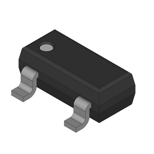
precision voltage reference is available in the subminiature (3 mm x 1.3 mm) SOT-23 surface-mount
package. The LM4051-N’s advanced design
eliminates the need for an external stabilizing
capacitor while ensuring stability with any capacitive
load, thus making the LM4051-N easy to use. Further
reducing design effort is the availability of a fixed
(1.225V) and adjust- able reverse breakdown voltage.
The minimum operating current is 60 μA for the
LM4051-1.2 and the LM4051-ADJ. Both versions
have a maximum operating current of 12 mA.
1
•
No Output Capacitor Required
Tolerates Capacitive Loads
Reverse Breakdown Voltage Options of 1.225 V
and Adjustable
Key Specifications:
– Output Voltage Tolerance (A Grade, 25 ̊C) ±
0.1% (Maximum)
– Output Noise (10 Hz to 10 kHz) 20 μV rms
– Operating Current Range: 60 μA to 12 mA
– Industrial Temp. Range: −40 ̊C to +85 ̊C
– Extended Temp. Range: −40 ̊C to +125 ̊C
– Temperature Coefficient: 50 ppm/ ̊C
(Maximum)
2 Applications
•
•
•
•
•
•
•
•
•
•
•
Portable, Battery-Powered Equipment
Data Acquisition Systems
Instrumentation
Process Control
Energy Management
Automotive and Industrial
Precision Audio Components
Base Stations
Battery Chargers
Medical Equipment
Communication
1.2 VREF Simplified Schematic
VDD
The LM4051-N comes in three grades (A, B, and C).
The best grade devices (A) have an initial accuracy of
0.1%, while the B-grade have 0.2% and the C-grade
0.5%, all with a tempco of 50 ppm/ ̊C guaranteed
from −40 ̊C to 125 ̊C.
The LM4051-N utilizes fuse and zener-zap trim of
reference voltage during wafer sort to ensure that the
prime parts have an accuracy of better than ± 0.1%
(A grade) at 25 ̊C.
Device Information(1)
PART NUMBER
LM4051-N
PACKAGE
SOT-23 (3)
BODY SIZE (NOM)
3.00 mm x 1.30 mm
(1) For all available packages, see the orderable addendum at
the end of the data sheet.
Adjustable Reference Simplified Schematic
VDD
RS
VOUT = 1.225 V
RS
Anode
VOUT = ADJ
R1
LM4051-1.2
LM4051-ADJ
Cathode
R2
1
An IMPORTANT NOTICE at the end of this data sheet addresses availability, warranty, changes, use in safety-critical applications,
intellectual property matters and other important disclaimers. PRODUCTION DATA.
�LM4051-N
SNOS491D – FEBRUARY 2000 – REVISED SEPTEMBER 2018
www.ti.com
Table of Contents
1
2
3
4
5
6
7
8
Features ..................................................................
Applications ...........................................................
Description .............................................................
Revision History.....................................................
Pin Configuration and Functions .........................
Specifications.........................................................
1
1
1
2
3
3
6.1
6.2
6.3
6.4
6.5
6.6
6.7
3
3
4
4
4
5
7
Absolute Maximum Ratings ......................................
ESD Ratings..............................................................
Recommended Operating Conditions.......................
Thermal Information ..................................................
LM4051-1.2 Electrical Characteristics ......................
LM4051-ADJ Electrical Characteristics.....................
Typical Characteristics ..............................................
Parameter Measurement Information .................. 9
Detailed Description ............................................ 10
8.1 Overview ................................................................. 10
8.2 Functional Block Diagram ....................................... 10
8.3 Feature Description................................................. 10
8.4 Device Functional Modes........................................ 10
9
Application and Implementation ........................ 11
9.1 Application Information............................................ 11
9.2 Typical Applications ................................................ 12
9.3 System Examples ................................................... 14
10 Power Supply Recommendations ..................... 18
11 Layout................................................................... 18
11.1 Layout Guidelines ................................................. 18
11.2 Layout Example .................................................... 18
12 Device and Documentation Support ................. 19
12.1
12.2
12.3
12.4
12.5
Receiving Notification of Documentation Updates
Community Resources..........................................
Trademarks ...........................................................
Electrostatic Discharge Caution ............................
Glossary ................................................................
19
19
19
19
19
13 Mechanical, Packaging, and Orderable
Information ........................................................... 19
4 Revision History
NOTE: Page numbers for previous revisions may differ from page numbers in the current version.
Changes from Revision C (March 2005) to Revision D
•
2
Page
Added Device Information table, Device Comparison table, ESD Ratings table, Feature Description section, Device
Functional Modes, Application and Implementation section, Power Supply Recommendations section, Layout
section, Device and Documentation Support section, and Mechanical, Packaging, and Orderable Information section. ..... 1
Submit Documentation Feedback
Copyright © 2000–2018, Texas Instruments Incorporated
Product Folder Links: LM4051-N
�LM4051-N
www.ti.com
SNOS491D – FEBRUARY 2000 – REVISED SEPTEMBER 2018
5 Pin Configuration and Functions
DBZ Package
1.2-V, 3-Pin SOT-23
Top View
DBZ Package
Adjustable, 3-Pin SOT-23
Top View
* This pin must be left floating or connected
to pin 2.
Pin Functions
PIN
I/O
DESCRIPTION
NAME
1.2 V
ADJ
Anode
2
3
O
Shunt Current/Voltage input
Cathode
1
2
I/O
Common pin, normally connected to ground
NC
3
-
-
Must float or connect to anode
FB
-
1
I
Threshold relative to cathode
6 Specifications
6.1 Absolute Maximum Ratings
over operating free-air temperature range (unless otherwise noted) (1)
MAX
UNIT
Reverse current
MIN
20
mA
Forward current
10
mA
Maximum output voltage (LM4051-ADJ)
15
V
Power dissipation (TA = 25°C) (2) M3 package
280
mW
Lead temperature M3 packages
Vapor phase (60 seconds)
215
Infrared (15 seconds)
220
Storage temperature, Tstg
(1)
(2)
–65
150
°C
°C
Stresses beyond those listed under Absolute Maximum Ratings may cause permanent damage to the device. These are stress ratings
only, which do not imply functional operation of the device at these or any other conditions beyond those indicated under Recommended
Operating Conditions. Exposure to absolute-maximum-rated conditions for extended periods may affect device reliability.
The maximum power dissipation must be derated at elevated temperatures and is dictated by TJmax (maximum junction temperature),
θJA (junction to ambient thermal resistance), and TA (ambient temperature). The maximum allowable power dissipation at any
temperature is PDmax= (TJmax −TA )/ θJA or the number given in the Absolute Maximum Ratings, whichever is lower. For the LM4051-N,
TJmax = 125°̊ C, and the typical thermal resistance (θJA), when board mounted, is 280°C/W for the SOT-23 package.
6.2 ESD Ratings
VALUE
V(ESD)
(1)
(2)
(3)
Electrostatic discharge
Human-body model (HBM), per ANSI/ESDA/JEDEC JS-001 (1) (2)
UNIT
±2000
Machine model (MM) (3)
200
V
JEDEC document JEP155 states that 500-V HBM allows safe manufacturing with a standard ESD control process.
The human body model is a 100-pF capacitor discharged through a 1.5-kΩ resistor into each pin.
The machine model is a 200-pF capacitor discharged directly into each pin.
Submit Documentation Feedback
Copyright © 2000–2018, Texas Instruments Incorporated
Product Folder Links: LM4051-N
3
�LM4051-N
SNOS491D – FEBRUARY 2000 – REVISED SEPTEMBER 2018
www.ti.com
6.3 Recommended Operating Conditions
over operating free-air temperature range (unless otherwise noted)
MIN
Temperature (Tmin ≤ TA ≤ Tmax)
Reverse current
Output voltage
NOM
MAX
Industrial temperature
–40
85
Extended temperature
–40
125
LM4051-1.2
0.06
12
LM4051-ADJ
0.06
12
LM4051-ADJ
1.24
10
UNIT
°C
mA
V
6.4 Thermal Information
THERMAL METRIC
LM4051-ADJ,
LM4051-1.2 V
(1)
UNIT
DBZ
3 PINS
RθJA
Junction-to-ambient thermal resistance
214.7
°C/W
RθJC(top)
Junction-to-case (top) thermal resistance
76.4
°C/W
RθJB
Junction-to-board thermal resistance
41.3
°C/W
ψJT
Junction-to-top characterization parameter
2.0
°C/W
ψJB
Junction-to-board characterization parameter
40.9
°C/W
(1)
For more information about traditional and new thermal metrics, see the Semiconductor and IC Package Thermal Metrics application
report.
6.5 LM4051-1.2 Electrical Characteristics
over operating free-air temperature range (unless otherwise noted)
PARAMETER
Reverse Breakdown
Voltage
TEST CONDITIONS
IR = 100 μA
±1.2
±2.4
(2)
±6
LM4051AIM3 (2)
±5.2 (1)
Industrial Temp. Range
TA = TJ = TMIN to TMAX
LM4051BIM3
LM4051CIM3 (2)
±10.1 (1)
Extended Temp. Range
TA = TJ = TMIN to TMAX
LM4051BEM3 (2)
±8.6 (1)
(2)
(1)
(2)
4
Minimum Operating
Current
UNIT
V
LM4051BIM3 LM4051BEM3 (2)
TJ = 25°C
IRMIN
MAX
LM4051AIM3 (2)
LM4051CIM3
Reverse Breakdown
Voltage Tolerance (1)
TYP
1.225
IR = 100 μA
VR
MIN
±6.4 (1)
mV
39
Industrial Temp. Range
TA = TJ = TMIN to TMAX
65
Extended Temp. Range
TA = TJ = TMIN to TMAX
70
µA
This overtemperature limit for Reverse Breakdown Voltage Tolerance is defined as the room temperature Reverse Breakdown Voltage
Tolerance ± [(∆VR/∆T)(max∆T)(VR)]. Where, ∆VR/∆T is the VR temperature coefficient, max∆T is the maximum difference in
temperature from the reference point of 25°̊ C to TMAX or TMIN, and VR is the reverse breakdown voltage. The total overtemperature
tolerance for the different grades in the industrial temperature range where max∆T=65 ̊C is shown below:
(a) A-grade: ± 0.425% = ± 0.1% ± 50 ppm/°̊ C x 65°̊ C
(b) B-grade: ± 0.525% = ± 0.2% ± 50 ppm/°̊ C x 65°̊ C
(c) C-grade: ± 0.825% = ± 0.5% ± 50 ppm/°̊ C x 65°̊ C
Therefore, as an example, the A-grade LM4051-1.2 has an over-temperature Reverse Breakdown Voltage tolerance of ± 1.2V x 0.425%
= ± 5.2 mV.
Limits are 100% production tested at 25 ̊C. Limits over temperature are guaranteed through correlation using Statistical Quality Control
(SQC) methods. The limits are used to calculate National’s AOQL.
Submit Documentation Feedback
Copyright © 2000–2018, Texas Instruments Incorporated
Product Folder Links: LM4051-N
�LM4051-N
www.ti.com
SNOS491D – FEBRUARY 2000 – REVISED SEPTEMBER 2018
LM4051-1.2 Electrical Characteristics (continued)
over operating free-air temperature range (unless otherwise noted)
PARAMETER
∆VR/∆T
Average Reverse
Breakdown Voltage
Temperature
Coefficient (1)
TEST CONDITIONS
MIN
IR =10 mA
∆VR/∆IR
MAX
UNIT
±20
IR =1 mA
±15
TJ = 25°C
IR = 100 μA
∆T = −40 ̊C to 125 ̊C
±50 (1)
TA = TJ = TMIN to TMAX
IRMIN ≤ IR ≤ 1 mA
0.3
Industrial Temp. Range
TA = TJ = TMIN to TMAX
1.1 (1)
Extended Temp. Range
TA = TJ = TMIN to TMAX
1.5 (1)
TJ = 25°C
1 mA ≤ IR ≤ 12 mA
ppm/ ̊C
±15
TJ = 25°C
Reverse Breakdown
Voltage Change with
Operating Current
Change
TYP
mV
1.8
Industrial Temp. Range
TA = TJ = TMIN to TMAX
6 (1)
Extended Temp. Range
TA = TJ = TMIN to TMAX
8 (1)
ZR
Reverse Dynamic
Impedance
IR = 1 mA, f = 120 Hz
0.5
Ω
eN
Wideband Noise
IR = 100 μA
10 Hz ≤ f ≤ 10 kHz
20
μVrms
∆VR
Reverse Breakdown
Voltage Long Term
Stability (3)
t = 1000 hrs, T = 25 ̊C ± 0.1 ̊C, IR = 100 μA
120
ppm
VHYST
Thermal Hysteresis (4)
∆T = −40 ̊C to 125 ̊C
0.36
mV/V
(3)
(4)
Long-term stability is VR at 25°̊ C measured during 1000 hrs.
Thermal hysteresis is defined as the difference in voltage measured at +25 ̊C after cycling to temperature –40 ̊C and the 25 ̊C
measurement after cycling to temperature +125 ̊C.
6.6 LM4051-ADJ Electrical Characteristics
over operating free-air temperature range (unless otherwise noted)
PARAMETER
Reference Voltage
TEST CONDITIONS
IR = 100 μA, VOUT = 5 V
IR = 100 μA, VOUT =5 V
VREF
Reference Voltage
Tolerance (1) (2)
(1)
(2)
(3)
TYP
MAX
1.212
UNIT
V
LM4051AIM3 (3)
±1.2
LM4051BIM3 (3)
±2.4
LM4051CIM3 (3)
±6
(3)
±5.2
LM4051AIM3
Industrial Temp. Range
TA = TJ = TMIN to TMAX
MIN
LM4051BIM3 (3)
±6.4
LM4051CIM3 (3)
±10.1
mV
This overtemperature limit for Reverse Breakdown Voltage Tolerance is defined as the room temperature Reverse Breakdown Voltage
Tolerance ± [(∆VR/∆T)(max∆T)(VR)]. Where, ∆VR/∆T is the VR temperature coefficient, max∆T is the maximum difference in temperature
from the reference point of 25°̊ C to TMAX or TMIN, and VR is the reverse breakdown voltage. The total overtemperature tolerance for the
different grades in the industrial temperature range where max∆T = 65 ̊C is shown below:
(a) A-grade: ± 0.425% = ± 0.1% ± 50 ppm/°̊ C × 65°̊ C
(b) B-grade: ± 0.525% = ± 0.2% ± 50 ppm/°̊ C × 65°̊ C
(c) C-grade: ± 0.825% = ± 0.5% ± 50 ppm/°̊ C × 65°̊ C
Therefore, as an example, the A-grade LM4051-1.2 has an overtemperature Reverse Breakdown Voltage tolerance of ± 1.2 V × 0.425%
= ± 5.2 mV.
Reference voltage and temperature coefficient will change with output voltage. See Typical Characteristics curves.
Limits are 100% production tested at 25 ̊C. Limits over temperature are ensured through correlation using Statistical Quality Control
(SQC) methods. The limits are used to calculate National’s AOQL.
Submit Documentation Feedback
Copyright © 2000–2018, Texas Instruments Incorporated
Product Folder Links: LM4051-N
5
�LM4051-N
SNOS491D – FEBRUARY 2000 – REVISED SEPTEMBER 2018
www.ti.com
LM4051-ADJ Electrical Characteristics (continued)
over operating free-air temperature range (unless otherwise noted)
PARAMETER
TEST CONDITIONS
Minimum Operating
Current
36
36
LM4051CIM3 (4)
∆VREF
/∆IR
∆VREF
/∆VO
Reference Voltage
Change with Output
Voltage Change
IFB
Feedback Current
(3)
60
LM4051BIM3 (3)
60
LM4051AIM3
LM4051CIM3
(3)
IRMIN ≤ IR ≤ 1 mA
VOUT ≥ 1.6 V (5)
1.1 (1)
TJ = 25°C
6 (1)
–1.69
Industrial Temp. Range
TA = TJ = TMIN to TMAX
–2.8 (1)
70
VOUT = 2.5 V
∆T = −40 ̊C to +125 ̊C
TJ = 25°C
IR = 1 mA
VOUT = VREF
0.3
VOUT = 10 V
2
eN
Wideband Noise
IR = 100 μA, VOUT = VREF, 10 Hz ≤ f ≤ 10 kHz
∆VREF
Reference Voltage Long
Term Stability (6)
VHYST
Thermal Hysteresis (7)
(5)
(6)
(7)
6
±50 (1)
15
IR = 1 mA, f = 120 Hz,
IAC = 0.1 IR
(4)
15
TJ = 25°C
IR =100 μA Industrial Temp. Range
TA = TJ = TMIN to TMAX
Dynamic Output
Impedance
nA
±50 (1)
Industrial Temp. Range
TA = TJ = TMIN to TMAX
ZOUT
130
mV
20
IR = 10 mA Industrial Temp. Range
TA = TJ = TMIN to TMAX
Average Reference
Voltage Temperature
Coefficient (Note 8)
mV
0.6
Industrial Temp. Range
TA = TJ = TMIN to TMAX
TJ = 25°C
IR = 0.1 mA
µA
0.3
Industrial Temp. Range
TA = TJ = TMIN to TMAX
1 mA ≤ IR ≤ 12 mA
VOUT ≥ 1.6 V (5)
UNIT
65
TJ = 25°C
TJ = 25°C
∆VREF
/∆T
MAX
36
Industrial Temp. Range
TA = TJ = TMIN to TMAX
Reference Voltage
Change with Operating
Current Change
TYP
LM4051BIM3 (4)
LM4051AIM3
IRMIN
MIN
(4)
ppm/°C
±50 (1)
Ω
20
µVrms
t = 1000 hrs, IR = 100 μA, T = 25 ̊C ± 0.1 ̊C
120
ppm
∆T = −40 ̊C to +125 ̊C
0.3
mV/V
Limits are 100% production tested at 25 ̊C. Limits over temperature are guaranteed through correlation using Statistical Quality Control
(SQC) methods. The limits are used to calculate National’s AOQL.
When VOUT ≤ 1.6 V, the LM4051-ADJ in the SOT-23 package must operate at reduced IR. This is caused by the series resistance of the
die attach between the die (–) output and the package (–) output pin. See the Output Saturation curve in the Typical Characteristics
section.
Long-term stability is VR at 25°̊ C measured during 1000 hrs.
Thermal hysteresis is defined as the difference in voltage measured at +25 ̊C after cycling to temperature –40 ̊C and the 25 ̊C
measurement after cycling to temperature +125 ̊C.
Submit Documentation Feedback
Copyright © 2000–2018, Texas Instruments Incorporated
Product Folder Links: LM4051-N
�LM4051-N
www.ti.com
SNOS491D – FEBRUARY 2000 – REVISED SEPTEMBER 2018
6.7 Typical Characteristics
Figure 1. Temperature Drift for Different Average
Temperature Coefficient
Figure 2. Output Impedance vs Frequency
Figure 3. Noise Voltage
Figure 4. Reverse Characteristics and Minimum Operating
Current
Figure 5. Start-Up Characteristics
Figure 6. Reference Voltage vs Output Voltage and
Temperature
Submit Documentation Feedback
Copyright © 2000–2018, Texas Instruments Incorporated
Product Folder Links: LM4051-N
7
�LM4051-N
SNOS491D – FEBRUARY 2000 – REVISED SEPTEMBER 2018
www.ti.com
Typical Characteristics (continued)
Figure 7. Reference Voltage vs Temperature and Output
Voltage
Figure 8. Feedback Current vs Output Voltage and
Temperature
Figure 9. Output Saturation (SOT-23 Only)
Figure 10. Output Impedance vs Frequency
Figure 11. Output Impedance vs Frequency
Figure 12. Reverse Characteristics
8
Submit Documentation Feedback
Copyright © 2000–2018, Texas Instruments Incorporated
Product Folder Links: LM4051-N
�LM4051-N
www.ti.com
SNOS491D – FEBRUARY 2000 – REVISED SEPTEMBER 2018
Typical Characteristics (continued)
Figure 13. Large Signal Response
Figure 14. Thermal Hysteresis
7 Parameter Measurement Information
Figure 15. Test Circuit for Start-Up Characteristics
Figure 16. Test Circuit for Reverse Characteristics
Figure 17. Test Circuit for Large Signal Response
Submit Documentation Feedback
Copyright © 2000–2018, Texas Instruments Incorporated
Product Folder Links: LM4051-N
9
�LM4051-N
SNOS491D – FEBRUARY 2000 – REVISED SEPTEMBER 2018
www.ti.com
8 Detailed Description
8.1 Overview
The LM4051-N is a precision voltage reference available in SOT-23 surface mount package. The LM4051-N is
available in a 1.225 V fixed-option as well as an adjustable voltage option. The LM4051-N comes in three
different tolerance grades (A, B, and C). The best grade devices (A) have an initial accuracy of 0.1%, while the
B-grade have 0.2% and the C-grade 0.5%, all with a temperature coefficient of 50 ppm/˚C guaranteed from
−40˚C to 125˚C.
8.2 Functional Block Diagram
*LM4051-ADJ only
**LM4051-1.2 only
8.3 Feature Description
The LM4051-N device is effectively a precision Zener diode. The part requires a small quiescent current for
regulation, and regulates the output voltage by shunting more or less current to ground, depending on input
voltage and load. The only external component requirement is a resistor between the cathode and the input
voltage to set the input current. An external capacitor can be used on the input or output, but is not required.
For the adjustable verson, feedback is applied from the Cathode and Reference pins, the LM4051-N behaves as
a Zener diode, regulating to a constant voltage dependent on current being supplied into the cathode. This is due
to the internal amplifier and reference entering the proper operating regions. The same amount of current needed
in the above feedback situation must be applied to this device in open loop, servo or error amplifying
implementations in order for it to be in the proper linear region giving the LM4051-N enough gain.
8.4 Device Functional Modes
8.4.1 LM4051-N - 1.2 V
The LM4051-N - 1.2V device is a fixed output voltage part, where the feedback is internal. Therefore, the part
can only operate is a closed loop mode and the output voltage cannot be adjusted. The output voltage will
remain in regulation as long as IR is between IRMIN. Proper selection of the external resistor for input voltage
range and load current range will ensure these conditions are met.
8.4.2 LM4051-N - ADJ
The majority of applications involving LM4051-N uses closed loop operation to regulate a fixed voltage or current.
The feedback enables this device to behave as an error amplifier, computing a portion of the output voltage and
adjusting it to maintain the desired regulation. This is done by relating the output voltage back to the reference
pin in a manner to make it equal to the internal reference voltage, which can be accomplished via resistive or
direct feedback.
10
Submit Documentation Feedback
Copyright © 2000–2018, Texas Instruments Incorporated
Product Folder Links: LM4051-N
�LM4051-N
www.ti.com
SNOS491D – FEBRUARY 2000 – REVISED SEPTEMBER 2018
9 Application and Implementation
NOTE
Information in the following applications sections is not part of the TI component
specification, and TI does not warrant its accuracy or completeness. TI’s customers are
responsible for determining suitability of components for their purposes. Customers should
validate and test their design implementation to confirm system functionality.
9.1 Application Information
The LM4051-N is a precision micro-power curvature-corrected bandgap shunt voltage reference. For space
critical applications, the LM4051-N is available in the sub-miniature SOT-23 surface-mount package. The
LM4051-N has been designed for stable operation without the need of an external capacitor connected between
the “+” pin and the “−” pin. If, however, a bypass capacitor is used, the LM4051-N remains stable. Design effort
is further reduced with the choice of either a fixed 1.2-V or an adjustable reverse breakdown voltage. The
minimum operating current is 60 μA for the LM4051-1.2 and the LM4051-ADJ. Both versions have a maximum
operating current of 12 mA.
LM4051-N's using the SOT-23 package have pin 3 connected as the (–) output through the package’s die attach
interface. Therefore, the LM4051-1.2’s pin 3 must be left floating or connected to pin 2 and the LM4051-ADJ’s
pin 3 is the (–) output.
The typical thermal hysteresis specification is defined as the change in +25 ̊C voltage measured after thermal
cycling. The device is thermal cycled to temperature –40 ̊C and then measured at 25 ̊C. Next the device is
thermal cycled to temperature +125 ̊C and again measured at 25 ̊C. The resulting VOUT delta shift between the
25 ̊C measurements is thermal hysteresis. Thermal hysteresis is common in precision references and is induced
by thermal-mechanical package stress. Changes in environmental storage temperature, operating temperature
and board mounting temperature are all factors that can contribute to thermal hysteresis.
In a conventional shunt regulator application (Figure 18), an external series resistor (RS) is connected between
the supply voltage and the LM4051-N. RS determines the current that flows through the load (IL) and the
LM4051-N (IQ). Since load current and supply voltage may vary, RS should be small enough to supply at least
the minimum acceptable IQ to the LM4051-N even when the supply voltage is at its minimum and the load
current is at its maximum value. When the supply voltage is at its maximum and IL is at its minimum, RS should
be large enough so that the current flowing through the LM4051-N is less than 12 mA.
RS should be selected based on the supply voltage, (VS), the desired load and operating current, (IL and IQ), and
the LM4051-N's reverse breakdown voltage, VR.
RS =
VS - VR
IL + IQ
(1)
The LM4051-ADJ’s output voltage can be adjusted to any value in the range of 1.24 V through 10 V. It is a
function of the internal reference voltage (VREF) and the ratio of the external feedback resistors as shown in
Figure 20. The output voltage is found using Equation 2:
VO = VREF éë(R2 / R1) + 1ùû
where
•
RS =
VO is the output voltage
(2)
VS - VR
IL + IQ + IF
(3)
The actual value of the internal VREF is a function of VO. The corrected VREF is determined by Equation 4:
VR EF = VO (D VR EF / D VO ) + VY
where
•
VY = 1.22 V
(4)
Submit Documentation Feedback
Copyright © 2000–2018, Texas Instruments Incorporated
Product Folder Links: LM4051-N
11
�LM4051-N
SNOS491D – FEBRUARY 2000 – REVISED SEPTEMBER 2018
www.ti.com
Application Information (continued)
∆VREF/∆VO is found in the LM4051-ADJ Electrical Characteristics and is typically −1.55 mV/V. You can get a
more accurate indication of the output voltage by replacing the value of VREF in Equation 2 with the value found
using Equation 4.
9.2 Typical Applications
9.2.1 Shunt Regulator
Figure 18. Shunt Regulator
9.2.1.1 Design Requirements
VIN > VOUT
Select RS such that:
IRMIN < IR < IRMAX where IRMAX = 12 mA
See LM4051-1.2 Electrical Characteristics for minimum operating current for each voltage option and grade.
9.2.1.2 Detailed Design Procedure
The resistor RS must be selected such that current, IR, will remain in the operational region of the part for the
entire VIN range and load current range. The two extremes to consider are VIN at its maximum, and the load at its
minimum, where RS must be large enough to main IR < IRMAX. For most desigins, 0.1 mA ≤ IR≤ 1 mA is a good
starting point.
Use cross and cross to set RS between RS_MIN and RS_MAX.
VIN _ MAX - VOUT
RS _ MIN =
ILOAD _ MIN + IR _ MAX
RS _ MAX =
12
(5)
VIN _ MIN - VOUT
ILOAD _ MAX + IR _ MIN
(6)
Submit Documentation Feedback
Copyright © 2000–2018, Texas Instruments Incorporated
Product Folder Links: LM4051-N
�LM4051-N
www.ti.com
SNOS491D – FEBRUARY 2000 – REVISED SEPTEMBER 2018
Typical Applications (continued)
9.2.1.3 Application Curves
Figure 19. Reverse Characteristics and Minimum Operating Current
9.2.2 Adjustable Shunt Regulator
Figure 20. Adjustable Shunt Regulator
9.2.2.1 Design Requirements
VIN > VOUT
Select RS such that:
IRMIN < IR < IRMAX where IRMAX = 12 mA
See LM4051-ADJ Electrical Characteristics for minimum operating current for each voltage option and grade.
9.2.2.2 Detailed Design Procedure
In order to program the cathode voltage to a regulated voltage a resistive bridge must be shunted between the
cathode and anode pins with the mid point tied to the reference pin. This can be seen in Figure 20, with R1 & R2
being the resistive bridge. The cathode/output voltage in the shunt regulator configuration can be approximated
by the equation shown in Equation 7. The cathode voltage can be more accurately determined by taking in to
account the cathode current shown in equation Equation 8.
R1 ·
§
VO = ¨1+
¸ × VREF
© R2¹
(7)
§ R1 ·
VO = ¨1+
¸ × VREF I REF × R1
© R2¹
(8)
Submit Documentation Feedback
Copyright © 2000–2018, Texas Instruments Incorporated
Product Folder Links: LM4051-N
13
�LM4051-N
SNOS491D – FEBRUARY 2000 – REVISED SEPTEMBER 2018
www.ti.com
Typical Applications (continued)
In order for this equation to be valid, LM4051-ADJ must be fully biased so that it has enough open loop gain to
mitigate any gain error. This can be done be meeting the IRMIN denoted in LM4051-ADJ Electrical Characteristics.
9.3 System Examples
Figure 21. Bounded Amplifier Reduces Saturation-induced Delays and Can Prevent Succeeding Stage
Damage. Nominal Clamping Voltage is ±VO (LM4051-N's Reverse Breakdown Voltage) +2 Diode VF .
Figure 22. Voltage Level Detector
Figure 23. Voltage Level Detector
14
Submit Documentation Feedback
Copyright © 2000–2018, Texas Instruments Incorporated
Product Folder Links: LM4051-N
�LM4051-N
www.ti.com
SNOS491D – FEBRUARY 2000 – REVISED SEPTEMBER 2018
System Examples (continued)
Figure 24. Fast Positive Clamp 2.4V + VD1
Figure 25. Bidirectional Clamp ± 2.4V
Figure 26. Bidirectional Adjustable Clamp ± 18V to ± 2.4V
Submit Documentation Feedback
Copyright © 2000–2018, Texas Instruments Incorporated
Product Folder Links: LM4051-N
15
�LM4051-N
SNOS491D – FEBRUARY 2000 – REVISED SEPTEMBER 2018
www.ti.com
System Examples (continued)
Figure 27. Bidirectional Adjustable Clamp ± 2.4V to ± 6V
Figure 28. Simple Floating Current Detector
*D1 can be any LED, VF = 1.5V to 2.2V at 3 mA. D1 may act as an indicator. D1 will be on if ITHRESHOLD falls below
the threshold current, except with I = O.
Figure 29. Current Source
16
Submit Documentation Feedback
Copyright © 2000–2018, Texas Instruments Incorporated
Product Folder Links: LM4051-N
�LM4051-N
www.ti.com
SNOS491D – FEBRUARY 2000 – REVISED SEPTEMBER 2018
System Examples (continued)
Figure 30. Precision Floating Current Detector
Figure 31. Precision 1 μA to 1 mA Current Source
Figure 32. Precision 1 μA to 1 mA Current Source
Submit Documentation Feedback
Copyright © 2000–2018, Texas Instruments Incorporated
Product Folder Links: LM4051-N
17
�LM4051-N
SNOS491D – FEBRUARY 2000 – REVISED SEPTEMBER 2018
www.ti.com
10 Power Supply Recommendations
While a bypass capacitor is not required on the input voltage line, TI recommends reducing noise on the input
which could affect the output. A 0.1-µF ceramic capacitor or larger is recommended.
In order to not exceed the maximum cathode current, be sure that the supply current is limited. For applications
shunting high currents, pay attention to the cathode and anode trace lengths, adjusting the width of the traces to
have proper current density.
11 Layout
11.1 Layout Guidelines
Bypass capacitors should be placed as close to the device as possible. Current-carrying traces need to have
widths appropriate for the amount of current they are carrying. Place RS as close as possible to the cathode.
Although not as critical, keep feedback resistor close to the device whenever possible.
11.2 Layout Example
RS physically close to device cathode
RS
CIN
COUT
CIN physically
close to device
COUT physically
close to device
Figure 33. Layout Diagram
RS physically close to device cathode
CIN physically close to device
COUT physically close to device
Figure 34. Feedback Resistors Layout Diagram
18
Submit Documentation Feedback
Copyright © 2000–2018, Texas Instruments Incorporated
Product Folder Links: LM4051-N
�LM4051-N
www.ti.com
SNOS491D – FEBRUARY 2000 – REVISED SEPTEMBER 2018
12 Device and Documentation Support
12.1 Receiving Notification of Documentation Updates
To receive notification of documentation updates, navigate to the device product folder on ti.com. In the upper
right corner, click on Alert me to register and receive a weekly digest of any product information that has
changed. For change details, review the revision history included in any revised document.
12.2 Community Resources
The following links connect to TI community resources. Linked contents are provided "AS IS" by the respective
contributors. They do not constitute TI specifications and do not necessarily reflect TI's views; see TI's Terms of
Use.
TI E2E™ Online Community TI's Engineer-to-Engineer (E2E) Community. Created to foster collaboration
among engineers. At e2e.ti.com, you can ask questions, share knowledge, explore ideas and help
solve problems with fellow engineers.
Design Support TI's Design Support Quickly find helpful E2E forums along with design support tools and
contact information for technical support.
12.3 Trademarks
E2E is a trademark of Texas Instruments.
All other trademarks are the property of their respective owners.
12.4 Electrostatic Discharge Caution
This integrated circuit can be damaged by ESD. Texas Instruments recommends that all integrated circuits be handled with
appropriate precautions. Failure to observe proper handling and installation procedures can cause damage.
ESD damage can range from subtle performance degradation to complete device failure. Precision integrated circuits may be more
susceptible to damage because very small parametric changes could cause the device not to meet its published specifications.
12.5 Glossary
SLYZ022 — TI Glossary.
This glossary lists and explains terms, acronyms, and definitions.
13 Mechanical, Packaging, and Orderable Information
The following pages include mechanical, packaging, and orderable information. This information is the most
current data available for the designated devices. This data is subject to change without notice and revision of
this document. For browser-based versions of this data sheet, refer to the left-hand navigation.
Table 1. SOT-23 Package Marking Information
PART MARKING
FIELD DEFINITION
RHA
RIA
RHB
RIB
First Field:
R = Reference
Second Field:
H = 1.225-V Voltage Option
I = Adjustable
RHC
RIC
Third Field:
A-C = Initial Reserved Breakdown
Voltage or Reference Voltage
Tolerance
A = ±0.1%, B = ±0.2%, C = ±0.5%
Submit Documentation Feedback
Copyright © 2000–2018, Texas Instruments Incorporated
Product Folder Links: LM4051-N
19
�IMPORTANT NOTICE AND DISCLAIMER
TI PROVIDES TECHNICAL AND RELIABILITY DATA (INCLUDING DATASHEETS), DESIGN RESOURCES (INCLUDING REFERENCE
DESIGNS), APPLICATION OR OTHER DESIGN ADVICE, WEB TOOLS, SAFETY INFORMATION, AND OTHER RESOURCES “AS IS”
AND WITH ALL FAULTS, AND DISCLAIMS ALL WARRANTIES, EXPRESS AND IMPLIED, INCLUDING WITHOUT LIMITATION ANY
IMPLIED WARRANTIES OF MERCHANTABILITY, FITNESS FOR A PARTICULAR PURPOSE OR NON-INFRINGEMENT OF THIRD
PARTY INTELLECTUAL PROPERTY RIGHTS.
These resources are intended for skilled developers designing with TI products. You are solely responsible for (1) selecting the appropriate
TI products for your application, (2) designing, validating and testing your application, and (3) ensuring your application meets applicable
standards, and any other safety, security, or other requirements. These resources are subject to change without notice. TI grants you
permission to use these resources only for development of an application that uses the TI products described in the resource. Other
reproduction and display of these resources is prohibited. No license is granted to any other TI intellectual property right or to any third
party intellectual property right. TI disclaims responsibility for, and you will fully indemnify TI and its representatives against, any claims,
damages, costs, losses, and liabilities arising out of your use of these resources.
TI’s products are provided subject to TI’s Terms of Sale (www.ti.com/legal/termsofsale.html) or other applicable terms available either on
ti.com or provided in conjunction with such TI products. TI’s provision of these resources does not expand or otherwise alter TI’s applicable
warranties or warranty disclaimers for TI products.
Mailing Address: Texas Instruments, Post Office Box 655303, Dallas, Texas 75265
Copyright © 2018, Texas Instruments Incorporated
�


 工商网监
湘ICP备2023018690号
工商网监
湘ICP备2023018690号
