19-1335; Rev 0a; 2/98
KIT
ATION
EVALU
E
L
B
AVAILA
Low-Power, 90Msps, 6-Bit ADC
Features
♦ High Sampling Rate: 90Msps
The MAX1011’s input amplifier features a true differential
input, a -0.5dB analog bandwidth of 55MHz, and a userprogrammable input full-scale range of 125mVp-p,
250mVp-p, or 500mVp-p. With an AC-coupled signal,
input offset is typically less than 1/4LSB. Dynamic performance is 5.85 effective number of bits (ENOB) with a
20MHz analog input signal, or 5.7 ENOB with a 50MHz
signal.
♦ Internal Bandgap Voltage Reference
The MAX1011 operates with +5V analog and +3.3V digital supplies for easy interfacing to +3.3V-logic-compatible
digital signal processors and microprocessors. It comes
in a 24-pin QSOP package.
♦ Single-Ended or Differential Input Drive
♦ Low Power Dissipation: 215mW
♦ Excellent Dynamic Performance:
5.85 ENOB with 20MHz Analog Input
5.7 ENOB with 50MHz Analog Input
♦ ±1/4LSB INL and DNL (typ)
♦ ±1/4LSB Input Offset (typ)
♦ Internal Oscillator with Overdrive Capability
♦ 55MHz (-0.5dB) Bandwidth Input Amplifier with
True Differential Input
♦ User-Selectable Full-Scale Range
(125mVp-p, 250mVp-p, or 500mVp-p)
♦ Flexible, 3.3V, CMOS-Compatible Digital Outputs
Applications
IF Sampling Receivers
VSAT Receivers
Wide Local Area Networks (WLANs)
Instrumentation
Ordering Information
PART
TEMP. RANGE
MAX1011CEG
0°C to +70°C
PIN-PACKAGE
24 QSOP
Pin Configuration appears at end of data sheet.
Functional Diagram
OCC+
OCC-
IN+
IN-
ADC
INPUT
AMP
6
DATA
BUFFER
VREF
OFFSET
CORRECTION
GAIN
6
CLOCK
OUT
BANDGAP
REFERENCE
CLOCK
DRIVER
D0–D5
DCLK
TNK+
TNK-
MAX1011
________________________________________________________________ Maxim Integrated Products
1
For free samples & the latest literature: http://www.maxim-ic.com, or phone 1-800-998-8800
For small orders, phone 408-737-7600 ext. 3468.
MAX1011
General Description
The MAX1011 is a 6-bit analog-to-digital converter
(ADC) that combines high-speed, low-power operation
with a user-selectable input range, an internal reference, and a clock oscillator. The ADC converts analog
signals into binary-coded digital outputs at sampling
rates up to 90Msps. The ability to directly interface with
baseband signals makes the MAX1011 ideal for use in
a wide range of communications and instrumentation
applications.
�MAX1011
Low-Power, 90Msps, 6-Bit ADC
ABSOLUTE MAXIMUM RATINGS
VCC to GND ..........................................................-0.3V to +6.5V
VCCO to OGND......................................................-0.3V to +6.5V
GND to OGND ......................................................-0.3V to +0.3V
Digital and Clock Output Pins to OGND...-0.3V to VCCO (10sec)
All Other Pins to GND...............................................-0.3V to VCC
Continuous Power Dissipation (TA = +70°C)
24-Pin QSOP (derate 10mW/°C above +70°C)...........800mW
Operating Temperature Range...............................0°C to +70°C
Storage Temperature Range .............................-65°C to +150°C
Lead Temperature (soldering,
很抱歉,暂时无法提供与“MAX1011CEG+”相匹配的价格&库存,您可以联系我们找货
免费人工找货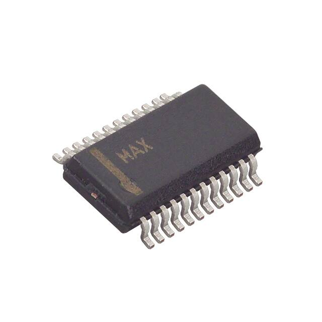


 工商网监
湘ICP备2023018690号
工商网监
湘ICP备2023018690号
