19-2853; Rev 4; 4/11
KIT
ATION
EVALU
E
L
B
A
AVAIL
10-Bit 300ksps ADCs with FIFO,
Temp Sensor, Internal Reference
The MAX1026/MAX1028/MAX1030 are serial 10-bit analog-to-digital converters (ADCs) with an internal reference
and an internal temperature sensor. These devices feature on-chip FIFO, scan mode, internal clock mode, internal averaging, and AutoShutdown™. The maximum
sampling rate is 300ksps using an external clock. The
MAX1030 has 16 input channels, the MAX1028 has 12
input channels, and the MAX1026 has 8 input channels.
All input channels are configurable for single-ended or
differential inputs in unipolar or bipolar mode. All three
devices operate from a +5V supply and contain a 10MHz
SPI™/QSPI™/MICROWIRE™-compatible serial port.
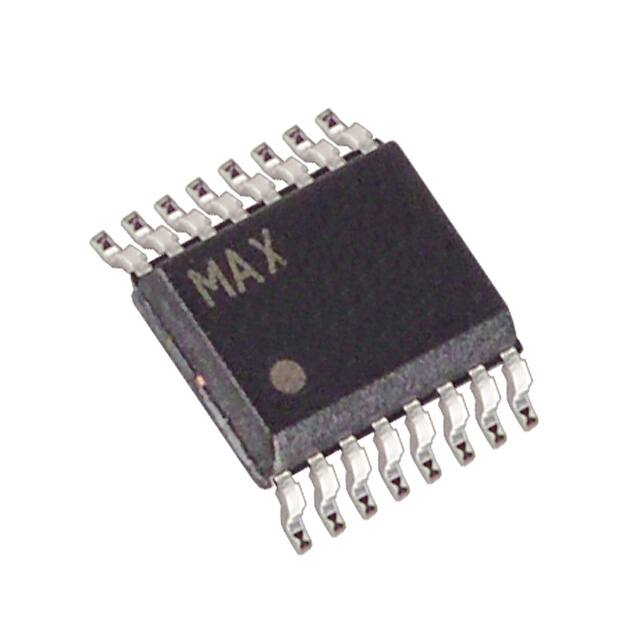
The MAX1030 is available in 28-pin 5mm x 5mm TQFN
with exposed pad and 24-pin QSOP packages. The
MAX1026/MAX1028 are only available in QSOP packages. All three devices are specified over the extended
-40°C to +85°C temperature range.
________________________Applications
System Supervision
Features
o Internal Temperature Sensor (±0.7°C Accuracy)
o 16-Entry First-In/First-Out (FIFO)
o Analog Multiplexer with True Differential
Track/Hold
16-, 12-, 8-Channel Single Ended
8-, 6-, 4-Channel True Differential
(Unipolar or Bipolar)
o Accuracy: ±1 LSB INL, ±1 LSB DNL, No Missing
Codes Over Temperature
o Scan Mode, Internal Averaging, and Internal Clock
o Low-Power Single +5V Operation
2.3mA at 300ksps
o Internal 4.096V Reference or External Differential
Reference
o 10MHz 3-Wire SPI/QSPI/MICROWIRE-Compatible
Interface
o Space-Saving 28-Pin 5mm x 5mm TQFN Package
Data-Acquisition Systems
Ordering Information
Industrial Control Systems
PART
Patient Monitoring
TEMP RANGE
PIN-PACKAGE
Data Logging
MAX1026BCEE+T
0°C to +70°C
16 QSOP
Instrumentation
MAX1026BEEE+T
-40°C to +85°C
16 QSOP
MAX1028BCEP+T
0°C to +70°C
20 QSOP
AutoShutdown is a trademark of Maxim Integrated Products, Inc.
SPI/QSPI are trademarks of Motorola, Inc.
MICROWIRE is a trademark of National Semiconductor Corp.
MAX1028BEEP+T
-40°C to +85°C
20 QSOP
+Denotes a lead(Pb)-free/RoHS-compliant package.
T = Tape and reel.
Ordering Information continued at end of data sheet.
Pin Configurations
+
TOP VIEW
AIN0 1
20 EOC
16 EOC
AIN1 2
19 DOUT
15 DOUT
AIN2 3
18 DIN
14 DIN
AIN3 4
13 CS
AIN4 5
AIN4 5
12 SCLK
AIN5 6
15 VDD
AIN5 6
11 VDD
AIN6 7
14 GND
REF-/AIN6 7
10 GND
AIN7 8
13 REF+
REF+
AIN8 9
12 CNVST/AIN11
AIN9 10
11 REF-/AIN10
AIN0 1
+
AIN1 2
AIN2 3
AIN3 4
MAX1026
9
CNVST/AIN7 8
QSOP
Pin Configurations continued at end of data sheet.
17 CS
MAX1028
16 SCLK
QSOP
________________________________________________________________ Maxim Integrated Products
For pricing, delivery, and ordering information, please contact Maxim Direct at 1-888-629-4642,
or visit Maxim’s website at www.maxim-ic.com.
1
MAX1026/MAX1028/MAX1030
General Description
�MAX1026/MAX1028/MAX1030
10-Bit 300ksps ADCs with FIFO,
Temp Sensor, Internal Reference
ABSOLUTE MAXIMUM RATINGS
VDD to GND ..............................................................-0.3V to +6V
CS, SCLK, DIN, EOC, DOUT to GND.........-0.3V to (VDD + 0.3V)
AIN0–AIN13, REF-/AIN_, CNVST/AIN_,
REF+ to GND.........................................-0.3V to (VDD + 0.3V)
Maximum Current into Any Pin............................................50mA
Continuous Power Dissipation (TA = +70°C)
16-Pin QSOP (derate 8.3mW/°C above +70°C)...........667mW
20-Pin QSOP (derate 9.1mW/°C above +70°C)...........727mW
24-Pin QSOP (derate 9.5mW/°C above +70°C)...........762mW
28-Pin TQFN 5mm x 5mm
(derate 20.8mW/°C above +70°C) ..........................1667mW
Operating Temperature Ranges
MAX10__C__.......................................................0°C to +70°C
MAX10__E__ ....................................................-40°C to +85°C
Storage Temperature Range .............................-60°C to +150°C
Junction Temperature ......................................................+150°C
Lead Temperature (soldering, 10s) .................................+300°C
Soldering Temperature (reflow) .......................................+260°C
Stresses beyond those listed under “Absolute Maximum Ratings” may cause permanent damage to the device. These are stress ratings only, and functional
operation of the device at these or any other conditions beyond those indicated in the operational sections of the specifications is not implied. Exposure to
absolute maximum rating conditions for extended periods may affect device reliability.
ELECTRICAL CHARACTERISTICS
(VDD = +5V ±5%, fSAMPLE = 300kHz, fSCLK = 4.8MHz (50% duty cycle), VREF = 4.096V, TA = TMIN to TMAX, unless otherwise noted.
Typical values are at TA = +25°C.)
PARAMETER
SYMBOL
CONDITIONS
MIN
TYP
MAX
UNITS
±1.0
LSB
±1.0
LSB
DC ACCURACY (Note 1)
Resolution
RES
Integral Nonlinearity
INL
Differential Nonlinearity
DNL
10
No missing codes over temperature
Offset Error
Gain Error
Bits
(Note 2)
±0.5
±2.0
LSB
±0.5
±2.0
LSB
±2
ppm/°C
FSR
Gain Temperature Coefficient
±0.8
ppm/°C
Channel-to-Channel Offset
Matching
±0.1
LSB
Offset Error Temperature
Coefficient
DYNAMIC SPECIFICATIONS (30kHz sine wave input, 4.096VP-P, 300ksps, fSCLK = 4.8MHz)
Signal-to-Noise Plus Distortion
SINAD
Total Harmonic Distortion
THD
Spurious-Free Dynamic Range
SFDR
Intermodulation Distortion
61
dB
-88
dBc
89
dBc
fIN1 = 29.9kHz, fIN2 = 30.2kHz
76
dBc
Full-Power Bandwidth
-3dB point
1
MHz
Full-Linear Bandwidth
S/(N + D) > 68dB
100
kHz
2
IMD
Up to the 5th harmonic
_______________________________________________________________________________________
�10-Bit 300ksps ADCs with FIFO,
Temp Sensor, Internal Reference
(VDD = +5V ±5%, fSAMPLE = 300kHz, fSCLK = 4.8MHz (50% duty cycle), VREF = 4.096V, TA = TMIN to TMAX, unless otherwise noted.
Typical values are at TA = +25°C.)
PARAMETER
SYMBOL
CONDITIONS
MIN
TYP
MAX
UNITS
CONVERSION RATE
Power-Up Time
tPU
Acquisition Time
tACQ
Conversion Time
tCONV
External Clock Frequency
fSCLK
External reference
0.8
Internal reference (Note 3)
65
Internally clocked
3.5
μs
0.6
Externally clocked (Note 4)
2.7
Externally clocked conversion
0.1
μs
μs
4.8
Data I/O
10
MHz
Aperture Delay
30
ns
Aperture Jitter
