MAX1204
5V, 8-Channel, Serial, 10-Bit ADC
with 3V Digital Interface
_______________General Description
____________________________Features
The MAX1204 is a 10-bit data-acquisition system
specifically designed for use in applications with mixed
+5V (analog) and +3V (digital) supply voltages. It operates with a single +5V analog supply or dual ±5V analog supplies, and combines an 8-channel multiplexer,
internal track/hold, and serial interface with high conversion speed and low power consumption.
o 8-Channel Single-Ended or 4-Channel Differential
Inputs
o Operates from +5V Single or ±5V Dual Supplies
o User-Adjustable Output Logic Levels (2.7V to
5.25V)
o Low Power: 1.5mA (Operating Mode)
2µA (Power-Down Mode)
o Internal Track/Hold, 133kHz Sampling Rate
o Internal 4.096V Reference
o SPI/MICROWIRE/TMS320-Compatible 4-Wire
Serial Interface
o Software-Configurable Unipolar/Bipolar Inputs
o 20-Pin PDIP/SSOP
o Pin-Compatible 12-Bit Upgrade: MAX1202
A 4-wire serial interface connects directly to
SPI/MICROWIRE® devices without external logic, and a
serial strobe output allows direct connection to
TMS320-family digital signal processors. The MAX1204
uses either the internal clock or an external serial-interface clock to perform successive-approximation analog-to-digital conversions. The serial interface operates
at up to 2MHz.
The MAX1204 features an internal 4.096V reference and
a reference-buffer amplifier that simplifies gain trim. It
also has a VL pin that supplies power to the digital outputs. Output logic levels (3V, 3.3V, or 5V) are determined
by the value of the voltage applied to this pin.
A hard-wired SHDN pin and two software-selectable
power-down modes are provided. Accessing the serial
interface automatically powers up the device. A quick
turn-on time allows the MAX1204 to be shut down
between conversions, enabling the user to optimize
supply currents. By customizing power-down between
conversions, supply current can drop below 10µA at
reduced sampling rates.
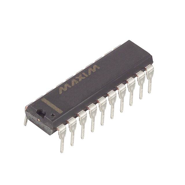
The MAX1204 is available in 20-pin SSOP and PDIP
packages, and is specified for the commercial and
extended temperature ranges.
______________Ordering Information
PART
TEMP RANGE
PINPACKAGE
TOP
MARK
MAX1204ACPP+
0°C to +70°C
20 PDIP
MAX1204BCPP+
0°C to +70°C
20 PDIP
±1/2
±1
MAX1204ACAP+
0°C to +70°C
20 SSOP
±1/2
MAX1204BCAP+
0°C to +70°C
20 SSOP
±1
Ordering Information continued at end of data sheet.
+Denotes a lead(Pb)-free/RoHS-compliant package.
__________________Pin Configuration
________________________Applications
5V/3V Mixed-Supply Systems
TOP VIEW
Data Acquisition
CH0
1
Process Control
CH1
2
Battery-Powered Instruments
CH2
3
Medical Instruments
+
20 VDD
19 SCLK
18 CS
MAX1204
CH3
4
CH4
5
16 SSTRB
CH5
6
15 DOUT
CH6
7
14 VL
CH7
8
13 GND
VSS
9
12 REFADJ
11 REF
SHDN 10
Typical Operating Circuit appears on last page.
MICROWIRE is a registered trademark of National Semiconductor Corp.
17 DIN
PDIP/SSOP
For pricing, delivery, and ordering information, please contact Maxim Direct
at 1-888-629-4642, or visit Maxim’s website at www.maximintegrated.com.
19-1179; Rev 1; 1/12
�MAX1204
5V, 8-Channel, Serial, 10-Bit ADC
with 3V Digital Interface
ABSOLUTE MAXIMUM RATINGS
VDD to GND ..............................................................-0.3V to +6V
VL................................................................-0.3V to (VDD + 0.3V)
VSS to GND...............................................................+0.3V to -6V
VDD to VSS ..............................................................-0.3V to +12V
CH0–CH7 to GND ............................(VSS - 0.3V) to (VDD + 0.3V)
CH0–CH7 Total Input Current...........................................±20mA
REF to GND ................................................-0.3V to (VDD + 0.3V)
REFADJ to GND .........................................-0.3V to (VDD + 0.3V)
Digital Inputs to GND .................................-0.3V to (VDD + 0.3V)
Digital Outputs to GND .................................-0.3V to (VL + 0.3V)
Digital Output Sink Current .................................................25mA
Continuous Power Dissipation (TA = +70°C)
PDIP (derate 11.11mW/°C above +70°C) .....................889mW
SSOP (derate 8.00mW/°C above +70°C) .....................640mW
Operating Temperature Ranges
MAX1204_C_P .....................................................0°C to +70°C
MAX1204_E_P ..................................................-40°C to +85°C
Storage Temperature Range .............................-60°C to +150°C
Soldering Temperature (reflow) .......................................+260°C
Stresses beyond those listed under “Absolute Maximum Ratings” may cause permanent damage to the device. These are stress ratings only, and functional
operation of the device at these or any other conditions beyond those indicated in the operational sections of the specifications is not implied. Exposure to
absolute maximum rating conditions for extended periods may affect device reliability.
ELECTRICAL CHARACTERISTICS
(VDD = +5V ±5%, VL = 2.7V to 3.6V; VSS = 0V or -5V ±5%; fSCLK = 2.0MHz, external clock (50% duty cycle); 15 clocks/conversion
cycle (133ksps); 4.7µF capacitor at REF; TA = TMIN to TMAX; unless otherwise noted.)
PARAMETER
SYMBOL
CONDITIONS
MIN
TYP
MAX
UNITS
DC ACCURACY (Note 1)
Resolution
10
Relative Accuracy (Note 2)
INL
Differential Nonlinearity
DNL
Offset Error
Gain Error (Note 3)
Gain Temperature Coefficient
Bits
MAX1204A
±0.5
MAX1204B
±1.0
No missing codes over temperature
±1.0
MAX1204A
±1.0
MAX1204B
±2.0
MAX1204A
±1.0
MAX1204B
±2.0
External reference, 4.096V
Channel-to-Channel
Offset Matching
LSB
LSB
LSB
LSB
±0.8
ppm/°C
±0.1
LSB
DYNAMIC SPECIFICATIONS (10kHz sine-wave input, 4.096VP-P, 133ksps, 2.0MHz external clock, bipolar input mode)
Signal-to-Noise + Distortion Ratio
SINAD
66
dB
Total Harmonic Distortion
(up to the 5th harmonic)
THD
-70
dB
Spurious-Free Dynamic Range
SFDR
70
dB
Channel-to-Channel Crosstalk
VIN = 4.096VP-P, 65kHz (Note 4)
-75
dB
Small-Signal Bandwidth
-3dB rolloff
4.5
MHz
800
kHz
Full-Power Bandwidth
2
Maxim Integrated
�MAX1204
5V, 8-Channel, Serial, 10-Bit ADC
with 3V Digital Interface
ELECTRICAL CHARACTERISTICS (continued)
(VDD = +5V ±5%, VL = 2.7V to 3.6V; VSS = 0V or -5V ±5%; fSCLK = 2.0MHz, external clock (50% duty cycle); 15 clocks/conversion
cycle (133ksps); 4.7µF capacitor at REF; TA = TMIN to TMAX; unless otherwise noted.)
PARAMETER
SYMBOL
CONDITIONS
MIN
TYP
MAX
UNITS
CONVERSION RATE
Conversion Time (Note 5)
tCONV
Track/Hold Acquisition Time
tACQ
Internal clock
External clock, 2MHz, 12 clocks/conversion
5.5
10
6
1.5
µs
µs
Aperture Delay
10
ns
Aperture Jitter
很抱歉,暂时无法提供与“MAX1204BCPP+”相匹配的价格&库存,您可以联系我们找货
免费人工找货