19-3759; Rev 0; 8/05
KIT
ATION
EVALU
E
L
B
A
AVAIL
1.8V, Dual, 12-Bit, 125Msps ADC for
Broadband Applications
The MAX1217 dual, monolithic, 12-bit, 125Msps analogto-digital converter (ADC) provides outstanding dynamic performance up to a 250MHz input frequency. The
device operates with conversion rates up to 125Msps
while consuming only 650mW per channel.
At 125Msps and an input frequency of 200MHz, the
MAX1217 achieves an 80dBc spurious-free dynamic
range (SFDR) with excellent 65.3dB signal-to-noise ratio
(SNR) at 200MHz. The SNR remains flat (within 3dB) for
input tones up to 200MHz. This makes the MAX1217
ideal for wideband applications such as communications
receivers, cable head-end receivers, and power-amplifier predistortion in cellular base-station transceivers.
The MAX1217 operates from a single 1.8V power supply. The analog inputs of each channel are designed
for AC-coupled, differential or single-ended operation.
The ADC also features a selectable on-chip divide-by-2
clock circuit that accepts clock frequencies as high as
250MHz and reduces the phase noise of the input
clock source. A low-voltage differential signal (LVDS)
sampling clock is recommended for best performance.
The converter’s digital outputs are LVDS compatible
and the data format can be selected to be either two’s
complement or offset binary.
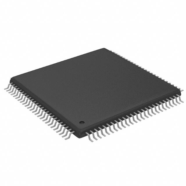
The MAX1217 is available in a 100-pin TQFP package
with exposed paddle and is specified over the extended (-40°C to +85°C) temperature range. Refer to the
MAX1218 (170Msps) and the MAX1219 (210Msps)
data sheets for higher speed, pin-compatible devices.
Features
� 125Msps Conversion Rate
� Excellent Low-Noise Characteristics
SNR = 67dB at fIN = 100MHz
SNR = 65.3dB at fIN = 200MHz
� Excellent Dynamic Range
SFDR = 85dBc at fIN = 100MHz
SFDR = 80dBc at fIN = 200MHz
� Single 1.8V Supply
� 1.3W Power Dissipation at fSAMPLE = 125Msps
and fIN = 10MHz
� On-Chip Track-and-Hold Amplifier
� Internal 1.24V Bandgap Reference
� On-Chip Selectable Divide-by-2 Clock Input
� LVDS Digital Outputs with Data Clock Output
� EV Kit Available (Order MAX1217EVKIT)
Ordering Information
PART
TEMP RANGE
PIN-PACKAGE
MAX1217ECQ -40°C to +85°C 100 TQFP-EP*
PKG
CODE
C100E-6
*EP = Exposed paddle.
Applications
Pin-Compatible Versions
Cable Modem Termination Systems (CMTS)
Cable Digital Return Path Transmitters
PART
RESOLUTION
(BITS)
SPEED GRADE
(Msps)
MAX1219
12
210
MAX1218
12
170
MAX1217
12
125
Cellular Base-Station Power-Amplifier Linearization
IF and Baseband Digitization
ATE and Instrumentation
Radar Systems
Pin Configuration appears at end of data sheet.
________________________________________________________________ Maxim Integrated Products
For pricing, delivery, and ordering information, please contact Maxim/Dallas Direct! at
1-888-629-4642, or visit Maxim’s website at www.maxim-ic.com.
1
MAX1217
General Description
�MAX1217
1.8V, Dual, 12-Bit, 125Msps ADC for
Broadband Applications
ABSOLUTE MAXIMUM RATINGS
AVCC to AGND ......................................................-0.3V to +2.1V
OVCC to OGND .....................................................-0.3V to +2.1V
OVCC to AVCC .......................................................-0.3V to +0.3V
OGND to AGND ....................................................-0.3V to +0.3V
CLKP, CLKN, INAP, INAN, INBP,
INBN to AGND .....................................-0.3V to (AVCC + 0.3V)
CLKDIV, T/BA, T/BB to AGND .................-0.3V to (AVCC + 0.3V)
REFA, REFADJA, REFB, REFADJB
to AGND...............................................-0.3V to (AVCC + 0.3V)
DCOP, DCON, DA0P–DA11P, DA0N–DA11N,
DB0P–DB11P, DB0N–DB11N, ORAP, ORAN,
ORBP, ORBN to OGND .......................-0.3V to (OVCC + 0.3V)
Current into any Pin.............................................................50mA
ESD Voltage on INAP, INAN, INBP, INBN
(Human Body Model).....................................................±750V
ESD Voltage on All Other Pins (Human Body Model)......±2000V
Continuous Power Dissipation (TA = +70°C)
100-Pin TQFP (derate 37mW/°C above +70°C).........2963mW
Operating Temperature Range ...........................-40°C to +85°C
Storage Temperature Range .............................-65°C to +150°C
Junction Temperature ......................................................+150°C
Lead Temperature (soldering, 10s) .................................+300°C
Stresses beyond those listed under “Absolute Maximum Ratings” may cause permanent damage to the device. These are stress ratings only, and functional
operation of the device at these or any other conditions beyond those indicated in the operational sections of the specifications is not implied. Exposure to
absolute maximum rating conditions for extended periods may affect device reliability.
DC ELECTRICAL CHARACTERISTICS
(AVCC = OVCC = +1.8V, AGND = OGND = 0, fSAMPLE = 125MHz, differential input and differential sine-wave clock signal, 0.1µF
capacitors on REFA and REFB, internal reference, digital output differential RL = 100Ω, TA = -40°C to +85°C, unless otherwise noted.
Typical values are at TA = +25°C.) (Note 1)
PARAMETER
SYMBOL
CONDITIONS
MIN
TYP
MAX
UNITS
DC ACCURACY
Resolution
N
12
Bits
Integral Nonlinearity (Note 2)
INL
fIN = 10MHz
-2
±0.6
+2
LSB
Differential Nonlinearity (Note 2)
DNL
No missing codes
-1
±0.3
+1
LSB
Transfer Curve Offset
VOS
TA = +25°C (Note 2)
-3
Offset Temperature Drift
+3
10
mV
µV/°C
ANALOG INPUTS (INAP, INAN, INBP, INBN)
Full-Scale Input Voltage Range
VFSR
TA = +25°C (Note 2)
1375
Full-Scale Range Temperature
Drift
1475
1625
mVP-P
150
ppm/°C
0.8
V
Common-Mode Input Range
VCM
Differential Input Capacitance
CIN
3
pF
Differential Input Resistance
RIN
1.8
kΩ
FPBW
800
MHz
Full-Power Analog Bandwidth
REFERENCE (REFA, REFB, REFADJA, REFADJB)
Reference Output Voltage
VREF_
TA = +25°C, REFADJ_ = AGND
1.18
Reference Temperature Drift
REFADJ_ Input High Voltage
1.24
65
VREFADJ_
Used to disable the internal reference
1.30
V
ppm/°C
AVCC 0.1
V
125
MHz
SAMPLING CHARACTERISTICS
Maximum Sampling Rate
fSAMPLE
Minimum Sampling Rate
fSAMPLE
2
40
_______________________________________________________________________________________
MHz
�1.8V, Dual, 12-Bit, 125Msps ADC for
Broadband Applications
(AVCC = OVCC = +1.8V, AGND = OGND = 0, fSAMPLE = 125MHz, differential input and differential sine-wave clock signal, 0.1µF
capacitors on REFA and REFB, internal reference, digital output differential RL = 100Ω, TA = -40°C to +85°C, unless otherwise noted.
Typical values are at TA = +25°C.) (Note 1)
MAX
UNITS
Clock Pulse-Width Low
PARAMETER
SYMBOL
tCL
Figure 5 (Note 3)
2
20
ns
Clock Pulse-Width High
tCH
Figure 5 (Note 3)
2
20
ns
Clock Duty Cycle
CONDITIONS
MIN
TYP
40 to
60
Set by clock-management circuit
%
Aperture Delay
tAD
Figures 5, 11
340
Aperture Jitter
tAJ
Figure 11
0.15
ps
psRMS
CLOCK INPUTS (CLKP, CLKN)
Differential Clock Input Amplitude
Clock Input Common-Mode
Voltage
(Note 3)
200
VCLKCM
Clock Differential Input
Resistance
RCLK
Clock Differential Input
Capacitance
CCLK
TA = +25°C (Note 3)
500
mVP-P
1.15
± 0.25
V
10
±25%
kΩ
3
pF
DYNAMIC CHARACTERISTICS (at -1dBFS) (Note 4)
Signal-to-Noise Ratio
SNR
fIN = 10MHz
65.2
67.7
fIN = 65MHz
65.2
67.5
fIN = 100MHz
fIN = 200MHz
Effective Number of Bits
ENOB
65.3
fIN = 10MHz
10.5
11
fIN = 65MHz
10.5
10.9
fIN = 100MHz
Spurious-Free Dynamic Range
SINAD
SFDR
Worst Harmonic
(HD2 or HD3)
Two-Tone Intermodulation
Distortion
TTIMD
10.6
fIN = 10MHz
65
fIN = 65MHz
65
67.6
67.4
fIN = 100MHz
66.8
fIN = 200MHz
65.1
fIN = 10MHz
72
fIN = 65MHz
72
fIN = 100MHz
Bits
10.8
fIN = 200MHz
Signal-to-Noise Plus Distortion
dB
67
dB
88
86
dBc
85
fIN = 200MHz
80
fIN = 10MHz
-88
-72
fIN = 65MHz
-86
-72
fIN = 100MHz
-85
fIN = 200MHz
-80
fIN1 = 29MHz at -7dBFS
fIN2 = 31MHz at -7dBFS
-92
fIN1 = 97MHz at -7dBFS
fIN2 = 100MHz at -7dBFS
-90
dBc
dBc
_______________________________________________________________________________________
3
MAX1217
DC ELECTRICAL CHARACTERISTICS (continued)
�MAX1217
1.8V, Dual, 12-Bit, 125Msps ADC for
Broadband Applications
DC ELECTRICAL CHARACTERISTICS (continued)
(AVCC = OVCC = +1.8V, AGND = OGND = 0, fSAMPLE = 125MHz, differential input and differential sine-wave clock signal, 0.1µF
capacitors on REFA and REFB, internal reference, digital output differential RL = 100Ω, TA = -40°C to +85°C, unless otherwise noted.
Typical values are at TA = +25°C.) (Note 1)
PARAMETER
SYMBOL
CONDITIONS
MIN
TYP
MAX
UNITS
CHANNEL CROSSTALK AND CHANNEL MATCHING SPECIFICATIONS
Channel Isolation
fIN = 200MHz, AIN = -1dBFS
90
dB
LVCMOS LOGIC INPUTS (CLKDIV, T/BA, T/BB)
Input High Voltage
VIH
Input Low Voltage
VIL
0.8 x
OVCC
V
0.2 x
OVCC
Input Capacitance
2
V
pF
LVDS DIGITAL OUTPUTS (DA0P/N–DA11P/N, DB0P/N–DB11P/N, ORAP/N, ORBP/N, DCOP/N)
Differential Output Voltage
|VOD|
225
490
mV
Output Offset Voltage
VOS
1.125
1.310
V
OUTPUT TIMING CHARACTERISTICS
CLK to Data Propagation Delay
tPDL
Figure 5 (Note 3)
1.7
ns
CLK to DCO Propagation Delay
tCPDL
Figure 5 (Note 3)
5.2
ns
DCO to Data Propagation Delay
tPDL - tCPDL (Note 3)
3.7
4.4
5.2
ns
LVDS Output Rise Time
tRL
20% to 80%, CL = 5pF
350
ps
LVDS Output Fall Time
tFL
20% to 80%, CL = 5pF
350
ps
Figure 5
11
Clock
Cycles
Output Data Pipeline Delay
tLATENCY
POWER REQUIREMENTS
Analog Supply Voltage Range
AVCC
1.71
Output Supply Voltage Range
OVCC
Analog Supply Current
IAVCC
fIN = 10MHz
Output Supply Current
IOVCC
fIN = 10MHz
Analog Power Dissipation
PDISS
fIN = 10MHz
Power-Supply Rejection Ratio
PSRR
(Note 5)
1.71
1.8
1.89
1.8
1.89
V
600
725
mA
120
160
mA
1.3
1.6
1
V
W
mV/V
Note 1: Values at TA = +25°C to +85°C are guaranteed by production test. Values at TA < +25°C are guaranteed by design and
characterization.
Note 2: Static linearity and offset parameters are computed from a best-fit straight line through the code transition points.
The full-scale range (FSR) is defined as 4095 x slope of the line.
Note 3: Parameter guaranteed by design and characterization; TA = -40°C to +85°C.
Note 4: ENOB and SINAD are computed from a curve fit.
Note 5: PSRR is measured with the analog and output supplies connected to the same potential.
4
_______________________________________________________________________________________
�1.8V, Dual, 12-Bit, 125Msps ADC for
Broadband Applications
-50
-60
-70
2
-80
10
-90
-40
-50
-60
7
5
4, 6
2
-80
5
4
-90
-100
50
fIN = 200.5996704MHz
fSAMPLE = 125MHz
AIN = -0.992dBFS
SINAD = 65.098dB
SNR = 65.341dB
THD = -77.742dBc
SFDR = 80.122dBc
HD2 = -82.718dBc
HD3 = -80.122dBc
3 2
-90
-40
-50
-60
-70
-80
0
-30
6
7
8
0
60
-40
-50
-60
23
-70
4 9
10
6
MAX1217 toc03
7
4 9
5
4 6 78
-90
9
10
20
30
40
FREQUENCY (MHz)
50
60
SNR/SINAD vs. ANALOG INPUT FREQUENCY
(fSAMPLE = 125MHz, AIN = -1dBFS)
fIN = 251.3046265MHz
fSAMPLE = 125MHz
AIN = -1.066dBFS
SINAD = 64.153dB
SNR = 64.484dB
THD = -75.496dBc
SFDR = 78.786dBc
HD2 = -78.977dBc
HD3 = -78.786dBc
-20
-80
5 10
-90
50
70
SNR
67
64
SINAD
61
10
58
-100
-110
0
10
20
30
40
FREQUENCY (MHz)
50
HD2/HD3 vs. ANALOG INPUT FREQUENCY
(fSAMPLE = 125MHz, AIN = -1dBFS)
HD2
20
30
40
FREQUENCY (MHz)
50
0
60
95
SFDR
90
50
100
150
200
ANALOG INPUT FREQUENCY (MHz)
250
100
150
200
250
SNR/SINAD vs. fSAMPLE
(fIN = 65.010071MHz, AIN = -1dBFS)
72
SNR
70
68
66
85
80
75
-THD
70
65
64
SINAD
62
60
58
56
60
54
55
52
50
50
0
50
ANALOG INPUT FREQUENCY (MHz)
100
SFDR/(-THD) (dBc)
HD3
10
SFDR/(-THD) vs. ANALOG INPUT FREQUENCY
(fSAMPLE = 125MHz, AIN = -1dBFS)
MAX1217 toc07
-50
-55
-60
-65
-70
-75
-80
-85
-90
-95
-100
-105
-110
55
0
60
SNR/SINAD (dB)
-110
MAX1217 toc09
-100
MAX1217 toc08
AMPLITUDE (dB)
-30
5
-110
20
30
40
FREQUENCY (MHz)
-10
AMPLITUDE (dB)
-20
23
-80
FFT PLOT
(16,384 SAMPLES)
MAX1217 toc04
0
HD2/HD3 (dBc)
10
6 8
10
FFT PLOT
(16,384 SAMPLES)
-10
-70
-100
0
60
-60
SNR/SINAD (dB)
20
30
40
FREQUENCY (MHz)
-50
MAX1217 toc05
10
-40
9 7
-110
0
-20
3
-100
-110
fIN = 100.4867554MHz
fSAMPLE = 125MHz
AIN = -1.092dBFS
SINAD = 66.84dB
SNR = 66.966dB
THD = -82.247dBc
SFDR = 85.865dBc
HD2 = -87.081dBc
HD3 = -85.865dBc
-30
-70
3
8
9
-30
0
-10
MAX1217 toc06
-40
-20
AMPLITUDE (dB)
AMPLITUDE (dB)
-30
fIN = 65.0100708MHz
fSAMPLE = 125MHz
AIN = -1.001dBFS
SINAD = 67.416dB
SNR = 67.514dB
THD = -83.914dBc
SFDR = 88.662dBc
HD2 = -89.221dBc
HD3 = -88.662dBc
-10
AMPLITUDE (dB)
fIN = 12.4893188MHz
fSAMPLE = 125MHz
AIN = -0.959dBFS
SINAD = 67.778dB
SNR = 67.9dB
THD = -83.336dBc
SFDR = 86.372dBc
HD2 = -86.372dBc
HD3 = -88.968dBc
-20
0
MAX1217 toc01
0
-10
FFT PLOT
(16,384 SAMPLES)
FFT PLOT
(16,384 SAMPLES)
MAX1217 toc02
FFT PLOT
(16,384 SAMPLES)
0
50
100
150
200
ANALOG INPUT FREQUENCY (MHz)
250
20
35
50
65
80
95
110
125
fSAMPLE (MHz)
_______________________________________________________________________________________
5
MAX1217
Typical Operating Characteristics
(AVCC = OVCC = +1.8V, fSAMPLE = 125MHz, differential input and differential sine-wave clock, 0.1µF capacitors on REFA and REFB,
digital output differential RL = 100Ω, TA = +25°C, unless otherwise noted.)
�Typical Operating Characteristics (continued)
(AVCC = OVCC = +1.8V, fSAMPLE = 125MHz, differential input and differential sine-wave clock, 0.1µF capacitors on REFA and REFB,
digital output differential RL = 100Ω, TA = +25°C, unless otherwise noted.)
85
80
75
-THD
70
65
60
65
50
80
95
110
35
50
65
80
95
110
125
-40
-15
10
35
60
IMD FFT PLOT
FFT PLOT
DIFFERENTIAL NONLINEARITY
vs. DIGITAL OUTPUT CODE
-25
2fIN1 - fIN2
-7dBFS
PER TONE
IMD = -92dBc
fIN2 = 31MHz
fIN1 = 29MHz
1.0
MAX1217 toc14
fIN = 10MHz
0.7
0.4
DNL (LSB)
fIN1 = 97MHz
0
AMPLITUDE (dBFS)
IMD = -90dBc
85
MAX1217 toc15
TEMPERATURE (°C)
2fIN2 - fIN1
-50
-75
2fIN2 - fIN1
2fIN1 - fIN2
0.1
-0.2
-100.2
-100
-0.5
-125.0
-125
-0.8
0
512 1024 1536 2048 2560 3072 3584 4095
FREQUENCY
FREQUENCY
DIGITAL OUTPUT CODE
INTEGRAL NONLINEARITY
vs. DIGITAL OUTPUT CODE
SNR/SINAD vs. ANALOG INPUT AMPLITUDE
(fSAMPLE = 125MHz, fIN = 65.010071MHz)
HD2/HD3 vs. ANALOG INPUT AMPLITUDE
(fSAMPLE = 125MHz, fIN = 65.010071MHz)
SNR
-0.3
HD2/HD3 (dBc)
SNR/SINAD (dB)
0
58
54
SINAD
50
46
42
-0.6
38
-0.9
512 1024 1536 2048 2560 3072 3584 4095
DIGITAL OUTPUT CODE
34
-30
-25
-20
-15
-10
-5
ANALOG INPUT AMPLITUDE (dBFS)
0
-50
-55
-60
-65
-70
-75
MAX1217 toc18
66
62
0.3
MAX1217 toc17
0.6
70
MAX1217 toc16
fIN = 10MHz
0
SNR AND SINAD
64
20
125
-50.7
0.9
MAX1217toc12
72
fSAMPLE (MHz)
fIN2 = 100MHz
-75.5
76
fSAMPLE (MHz)
-7dBFS
PER TONE
-26.0
SFDR
68
50
35
80
55
HD2
-1.2
6
84
SNR/SINAD, SFDR (dB, dBc)
SFDR
90
88
MAX1217 toc11
95
SFDR/(-THD) (dBc)
HD3
20
LOG MAGNITUDE (dBFS)
100
MAX1217 toc10
-50
-55
-60
-65
-70
-75
-80
-85
-90
-95
-100
-105
-110
SNR/SINAD, SFDR vs. TEMPERATURE
(fIN = 10MHz, AIN = -1dBFS)
SFDR/(-THD) vs. fSAMPLE
(fIN = 65.010071MHz, AIN = -1dBFS)
MAX1217 toc13
HD2/HD3 (dBc)
HD2/HD3 vs. fSAMPLE
(fIN = 65.010071MHz, AIN = -1dBFS)
INL (LSB)
MAX1217
1.8V, Dual, 12-Bit, 125Msps ADC for
Broadband Applications
HD3
-80
-85
-90
-95
-100
-105
-110
HD2
-30
-25
-20
-15
-10
-5
ANALOG INPUT AMPLITUDE (dBFS)
_______________________________________________________________________________________
0
�1.8V, Dual, 12-Bit, 125Msps ADC for
Broadband Applications
SNR
68
-65
-70
75
70
65
-THD
-75
66
SINAD
HD2/HD3 (dBc)
SNR/SINAD (dB)
SFDR
80
64
62
HD2
-80
-85
-90
-95
60
HD3
-100
60
55
MAX1217 toc21
-60
MAX1217 toc20
85
-105
-110
58
-25
-20
-15
-10
-5
-5
0
-4
-3
-2
-1
0
1
2
SFDR/(-THD) vs. % FS ADJUSTMENT
(fSAMPLE = 125MHz, fIN = 12.5MHz, AIN = -1dBFS)
100
95
3
4
5
-5
-4
SFDR
90
-3
-2
-1
0
1
2
3
4
5
FULL-SCALE ADJUSTMENT (%)
FULL-SCALE ADJUSTMENT (%)
ANALOG INPUT AMPLITUDE (dBFS)
FS VOLTAGE vs. ADJUST RESISTOR
1.34
MAX1217 toc22
1.32
1.30
1.28
85
RESISTOR VALUE APPLIED BETWEEN
REFADJA/REFADJB AND
REFA/REFB INCREASES VFS
1.26
80
VFS (V)
-30
MAX1217 toc23
50
SFDR/(-THD) (dBc)
SFDR/(-THD) (dBc)
70
MAX1217 toc19
90
HD2/HD3 vs. % FS ADJUSTMENT
(fSAMPLE = 125MHz, fIN = 12.5MHz, AIN = -1dBFS)
SNR/SINAD vs. % FS ADJUSTMENT
(fSAMPLE = 125MHz, fIN = 12.5MHz, AIN = -1dBFS)
SFDR/(-THD) vs. ANALOG INPUT AMPLITUDE
(fSAMPLE = 125MHz, fIN = 65.010071MHz)
-THD
75
1.24
70
1.22
65
1.20
60
1.18
55
1.16
RESISTOR VALUE APPLIED BETWEEN
REFADJA/REFADJB AND
AGND DECREASES VFS
1.14
50
-5
-4
-3
-2
-1
0
1
2
3
FULL-SCALE ADJUSTMENT (%)
4
5
0 100 200 300 400 500 600 700 800 900 1000
FS ADJUST RESISTOR (kΩ)
_______________________________________________________________________________________
7
MAX1217
Typical Operating Characteristics (continued)
(AVCC = OVCC = +1.8V, fSAMPLE = 125MHz, differential input and differential sine-wave clock, 0.1µF capacitors on REFA and REFB,
digital output differential RL = 100Ω, TA = +25°C, unless otherwise noted.)
�1.8V, Dual, 12-Bit, 125Msps ADC for
Broadband Applications
MAX1217
Pin Description
PIN
NAME
FUNCTION
REFA
Channel A Reference Input/Output. Channel A 1.24V reference output when REFADJA is driven
low. Channel A external reference input when REFADJA is driven high. Connect a 0.1µF capacitor
from REFA to AGND with both external and internal references.
2
REFADJA
Channel A Reference Adjust Input. REFADJA allows for full-scale range adjustments by placing a
resistor or trim potentiometer between REFADJA and AGND (decreases FS range) or REFADJA
and REFA (increases FS range). Connect REFADJA to AVCC to overdrive the internal reference
with an external reference. Connect REFADJA to AGND to allow the internal reference to
determine the full-scale range of the data converter. See the FSR Adjustments Using the Internal
Bandgap Reference section.
3, 5, 8, 11, 14, 18,
21, 23, 26, 28, 30,
33, 93, 96, 99, 100
AGND
Analog Converter Ground
4, 9, 10, 15, 16,
17, 22, 27, 29, 31,
94, 95
AVCC
Analog Supply Voltage. Bypass AVCC to AGND with a 0.1µF capacitor for best decoupling
results. Use additional board decoupling. See the Grounding, Bypassing, and Layout
Considerations section.
6
INAP
Positive Analog Input A. Positive analog input to channel A.
1
8
7
INAN
Negative Analog Input A. Negative analog input to channel A.
12
CLKP
True Clock Input. Apply an LVDS-compatible input level to CLKP.
13
CLKN
Complementary Clock Input. Apply an LVDS-compatible input level to CLKN.
19
INBN
Negative Analog Input B. Negative analog input to channel B.
20
INBP
Positive Analog Input B. Positive analog input to channel B.
24
REFADJB
Channel B Reference Adjust Input. REFADJB allows for full-scale range adjustments by placing a
resistor or trim potentiometer between REFADJB and AGND (decreases FS range) or REFADJB
and REFA (increases FS range). Connect REFADJB to AVCC to overdrive the internal reference
with an external reference. Connect REFADJB to AGND to allow the internal reference to
determine the full-scale range of the data converter. See the FSR Adjustments Using the Internal
Bandgap Reference section.
25
REFB
Channel B Reference Input/Output. Channel B 1.24V reference output when REFADJB is driven
low. Channel B external reference input when REFADJB is driven high. Connect a 0.1µF capacitor
from REFB to AGND with both external and internal references.
Clock-Divider Input. CLKDIV controls the sampling frequency relative to the input clock
frequency. CLKDIV has an internal pulldown resistor.
CLKDIV = 0: Sampling frequency is one-half the input clock frequency.
CLKDIV = 1: Sampling frequency is equal to the input clock frequency.
32
CLKDIV
34, 62, 92
OVCC
Output Stage Supply Voltage. Bypass OVCC with a 0.1µF capacitor to AGND. Use additional
board decoupling. See the Grounding, Bypassing, and Layout Considerations section.
35
ORBP
Channel B True Differential Over-Range Output
36
ORBN
Channel B Complementary Differential Over-Range Output
37
DB11P
Channel B True Differential Digital Output Bit 11 (MSB)
38
DB11N
Channel B Complementary Differential Digital Output Bit 11 (MSB)
39
DB10P
Channel B True Differential Digital Output Bit 10
40
DB10N
Channel B Complementary Differential Digital Output Bit 10
41
DB9P
Channel B True Differential Digital Output Bit 9
42
DB9N
Channel B Complementary Differential Digital Output Bit 9
_______________________________________________________________________________________
�1.8V, Dual, 12-Bit, 125Msps ADC for
Broadband Applications
PIN
NAME
43
DB8P
Channel B True Differential Digital Output Bit 8
FUNCTION
44
DB8N
Channel B Complementary Differential Digital Output Bit 8
45
DB7P
Channel B True Differential Digital Output Bit 7
46
DB7N
Channel B Complementary Differential Digital Output Bit 7
47
DB6P
Channel B True Differential Digital Output Bit 6
48
DB6N
Channel B Complementary Differential Digital Output Bit 6
49
DB5P
Channel B True Differential Digital Output Bit 5
50
DB5N
Channel B Complementary Differential Digital Output Bit 5
51
DB4P
Channel B True Differential Digital Output Bit 4
52
DB4N
Channel B Complementary Differential Digital Output Bit 4
53
DB3P
Channel B True Differential Digital Output Bit 3
54
DB3N
Channel B Complementary Differential Digital Output Bit 3
55
DB2P
Channel B True Differential Digital Output Bit 2
56
DB2N
Channel B Complementary Differential Digital Output Bit 2
57
DB1P
Channel B True Differential Digital Output Bit 1
58
DB1N
Channel B Complementary Differential Digital Output Bit 1
59
DB0P
Channel B True Differential Digital Output Bit 0 (LSB)
60
DB0N
Channel B Complementary Differential Digital Output Bit 0 (LSB)
61, 63
OGND
Output Stage Ground. Ground connection for output circuitry.
64
DCON
Complementary LVDS Digital Clock Output. Outputs same frequency as ADC sampling frequency.
65
DCOP
True LVDS Digital Clock Output. Outputs same frequency as ADC sampling frequency.
66
DA0N
Channel A Complementary Differential Digital Output Bit 0 (LSB)
67
DA0P
Channel A True Differential Digital Output Bit 0 (LSB)
68
DA1N
Channel A Complementary Differential Digital Output Bit 1
69
DA1P
Channel A True Differential Digital Output Bit 1
70
DA2N
Channel A Complementary Differential Digital Output Bit 2
71
DA2P
Channel A True Differential Digital Output Bit 2
72
DA3N
Channel A Complementary Differential Digital Output Bit 3
73
DA3P
Channel A True Differential Digital Output Bit 3
74
DA4N
Channel A Complementary Differential Digital Output Bit 4
75
DA4P
Channel A True Differential Digital Output Bit 4
76
DA5N
Channel A Complementary Differential Digital Output Bit 5
77
DA5P
Channel A True Differential Digital Output Bit 5
78
DA6N
Channel A Complementary Differential Digital Output Bit 6
79
DA6P
Channel A True Differential Digital Output Bit 6
80
DA7N
Channel A Complementary Differential Digital Output Bit 7
81
DA7P
Channel A True Differential Digital Output Bit 7
82
DA8N
Channel A Complementary Differential Digital Output Bit 8
83
DA8P
Channel A True Differential Digital Output Bit 8
84
DA9N
Channel A Complementary Differential Digital Output Bit 9
_______________________________________________________________________________________
9
MAX1217
Pin Description (continued)
�1.8V, Dual, 12-Bit, 125Msps ADC for
Broadband Applications
MAX1217
Pin Description (continued)
PIN
NAME
85
DA9P
86
DA10N
FUNCTION
Channel A True Differential Digital Output Bit 9
Channel A Complementary Differential Digital Output Bit 10
87
DA10P
Channel A True Differential Digital Output Bit 10
88
DA11N
Channel A Complementary Differential Digital Output Bit 11 (MSB)
89
DA11P
Channel A True Differential Digital Output Bit 11 (MSB)
90
ORAN
Channel B Complementary Differential Over-Range Output
91
ORAP
Channel B True Differential Over-Range Output
T/BB
Output Format Select Input for Channel B. T/BB controls the digital output format of channel B of
the MAX1217. T/BB has an internal pulldown resistor.
T/BB = 1: Binary output format.
T/BB = 0: Two’s-complement output format.
98
T/BA
Output Format Select Input for Channel A. T/BA controls the digital output format of channel A of
the MAX1217. T/BA has an internal pulldown resistor.
T/BA = 1: Binary output format.
T/BA = 0: Two’s-complement output format.
—
EP
97
Exposed Paddle. The exposed paddle is located on the backside of the device and must be
connected to AGND.
AVCC
OVCC
INAP
T/H
INAN
1kΩ
12-BIT PIPELINE
ADC
CHANNEL A
MAX1217
1kΩ
DCOP
DCON
1kΩ
INBN
T/H
INBP
AGND
CKLP
CKLN
CLKDIV
LVDS DATA PORT
1kΩ
DIV1/DIV2
CLOCK
MANAGEMENT
REFERENCE
REFADJA
REFA
REFB
REFADJB
12-BIT PIPELINE
ADC
CHANNEL B
DA0_–DA11_
ORAP/ORAN
T/BA/B
ORBP/ORBN
DB0_–DB11_
OGND
Figure 1. Functional Diagram
10
______________________________________________________________________________________
�1.8V, Dual, 12-Bit, 125Msps ADC for
Broadband Applications
Theory of Operation
The MAX1217 uses a fully differential pipelined architecture that allows for high-speed conversion, optimized accuracy, and linearity while minimizing power
consumption.
Both positive inputs (INAP, INBP) and negative/complementary analog inputs (INAN, INBN) are centered
around a 0.8V common-mode voltage, and each
accept a ±V FS / 4 differential analog input voltage
swing, providing a 1.475VP-P typical differential fullscale signal swing. Each set of inputs (INAP, INAN and
INBP, INBN) is sampled when the differential sampling
clock signal transitions high. When using the clockdivide mode, the analog inputs are sampled at every
other high transition of the differential sampling clock.
Each pipeline converter stage converts its input voltage
to a digital output code. At every stage, except the last,
the error between the input voltage and the digital output code is multiplied and passed along to the next
pipeline stage. Digital error correction compensates for
ADC comparator offsets in each pipeline stage and
ensures no missing codes. The result is a 12-bit parallel
digital output word in selectable two’s-complement or
offset binary output formats with LVDS-compatible output levels (Figure 1).
Analog Inputs
The MAX1217 features two sets of fully differential
inputs (INAP, INAN and INBP, INBN) for each input
channel. Differential inputs feature good rejection of
even-order harmonics, which allows for enhanced AC
performance as the signals are progressing through
the analog stages. The MAX1217 analog inputs are
self-biased at a 0.8V common-mode voltage and allow
a 1.475VP-P differential input voltage swing (Figure 2).
Both sets of inputs are self-biased through 1kΩ resistors, resulting in a typical 2kΩ differential input resistance. Drive the analog inputs of the MAX1217 in
AC-coupled configuration to achieve best dynamic performance. See the Transformer-Coupled, Differential
Analog Input Drive section.
On-Chip Reference Circuit
The MAX1217 features an internal 1.24V bandgap reference circuit (Figure 3), which, in combination with two
internal reference-scaling amplifiers, determines the
FSR of each channel. Bypass REFA and REFB with a
0.1µF capacitor to AGND. Adjust the voltage of the
bandgap reference for each channel independently by
adding an external resistor (e.g., 100kΩ trim potentiometer) between REFADJA/REFADJB and AGND or
REFADJA/REFADJB and REFA/REFB to compensate
for gain errors or increase the FSR of each channel.
See the Applications Information section for a detailed
description of this process.
To disable the internal reference for each channel, connect the reference adjust input (REFADJA, REFADJB)
to AVCC. Apply an external, stable reference to the
channel’s reference input/output (REFA, REFB) to set
the converter’s full scale. To enable the internal reference for a channel, connect the appropriate reference
adjust input (REFADJA, REFADJB) to AGND.
Clock Inputs (CLKP, CLKN)
Drive the clock inputs of the MAX1217 with an LVDScompatible clock to achieve the best dynamic performance. The clock signal source must be a high-quality,
low phase noise to avoid any degradation in the noise
performance of the ADC. The clock inputs (CLKP,
CLKN) are internally biased to 1.15V to accept a typical
0.5VP-P differential signal swing (Figure 4). See the
Differential, AC-Coupled LVPECL-Compatible Clock
Input section for more circuit details on how to drive
CLKP and CLKN appropriately. Although not recommended, the clock inputs also accept a single-ended
input signal.
The MAX1217 also features an internal clock-management circuit (duty-cycle equalizer) to ensure that the
clock signal applied to inputs CLKP and CLKN is
processed to provide a 50% duty-cycle clock signal that
desensitizes the performance of the converter to variations in the duty cycle of the input clock source. The
clock duty-cycle equalizer cannot be turned off externally and requires a minimum 40MHz clock frequency to
allow the device to meet data sheet specifications.
If the MAX1217 is not clocked, the digital outputs begin
to change state randomly, resulting in a supply current
increase of up to 40mA.
Clock Outputs (DCON, DCOP)
The MAX1217 features a differential clock output, which
can be used to latch the digital output data with an
external latch or receiver. Additionally, the clock output
can be used to synchronize external devices (e.g.,
FPGAs) to the ADC. DCOP and DCON are differential
outputs with LVDS-compatible voltage levels. There is a
5.2ns (typ) delay between the rising (falling) edge of
CLKP (CLKN) and the rising (falling) edge of DCOP
(DCON). See Figure 5 for timing details.
Divide-by-2 Clock Control
The MAX1217 offers a clock control line (CLKDIV) that
supports the reduction of clock jitter in a system.
Connect CLKDIV to OGND to enable the ADC’s internal
______________________________________________________________________________________
11
MAX1217
Detailed Description
�MAX1217
1.8V, Dual, 12-Bit, 125Msps ADC for
Broadband Applications
AVCC
T/H
MAX1217
IN_P
CP
1kΩ
CS
12-BIT PIPELINE
ADC
1kΩ
CS
IN_N
CP
FROM CLOCK-MANAGEMENT BLOCK
TO COMMON MODE
CS IS THE SAMPLING CAPACITANCE
CP IS THE PARASITIC CAPACITANCE ~ 1pF
VCM + VFS / 4
IN_P
VCM
IN_N
VCM - VFS / 4
GND
+VFS / 2
GND
1.4V DIFFERENTIAL FSR
IN_P - IN_N
-VFS / 2
Figure 2. Simplified Analog Input Architecture and Allowable Input Voltage Range
divide-by-2 clock divider. Data is now updated at onehalf the ADC’s input clock rate. CLKDIV has an internal
pulldown resistor and can be left open for applications
12
that require this divide-by-2 mode. Connecting CLKDIV
to OVCC disables the divide-by-2 mode.
______________________________________________________________________________________
�1.8V, Dual, 12-Bit, 125Msps ADC for
Broadband Applications
REFTA
G
MAX1217
CHANNEL A
FULL SCALE = REFTA - REFBA
REFERENCESCALING
AMPLIFIER
REFBA
REFERENCE
BUFFER
REFA
0.1μF
MAX1217
REFADJA*
CONTROL LINE
TO DISABLE
REFERENCE BUFFER
1V
AVCC / 2
AVCC
CHANNEL B
FULL SCALE = REFTB - REFBB
REFTB
G
REFERENCESCALING
AMPLIFIER
REFBB
REFERENCE
BUFFER
REFB
0.1μF
REFADJB*
CONTROL LINE
TO DISABLE
REFERENCE BUFFER
AVCC
AVCC / 2
*REFADJA/B CAN BE SHORTED TO AGND THROUGH
A 1kΩ RESISTOR OR POTENTIOMETER.
REFT_: TOP OF REFERENCE LADDER
REFB_: BOTTOM OF REFERENCE LADDER
Figure 3. Simplified Reference Architecture
System Timing Requirements
Figure 5 depicts the relationship between the clock
input and output, analog input, sampling event, and
data output. The MAX1217 samples on the rising
(falling) edge of CLKP (CLKN). Output data is valid on
the next rising (falling) edge of DCOP (DCON), with an
internal latency of 11 clock cycles.
Digital Outputs (DA0P/N–DA11P/N,
DB0P/N–DB11P/N, ORAP/N, ORBP/N,
DCOP/N) and Control Inputs T/BA, T/BB
Digital outputs DA0P/N–DA11P/N, DB0P/N–DB11P/N,
ORAP/N, ORBP/N, and DCOP/N are LVDS compatible,
and data on DA0P/N–DA11P/N and DB0P/N–DB11P/N
are presented in either binary or two’s-complement format (Table 1). The T/BA, T/BB control lines are LVCMOScompatible inputs that allow a selectable output format
for each channel. Pulling T/BA, T/BB low outputs data in
two’s complement and pulling it high presents data in
offset binary format on each of the channels’ 12-bit parallel buses. T/BA, T/BB have an internal pulldown resistor and can be left unconnected in applications using
______________________________________________________________________________________
13
�MAX1217
1.8V, Dual, 12-Bit, 125Msps ADC for
Broadband Applications
Note: Although a differential LVDS output architecture
reduces single-ended transients to the supply and
ground planes, capacitive loading on the digital outputs should still be kept as low as possible. Using
LVDS buffers on the digital outputs of the ADC when
driving larger loads improves overall performance and
reduces system-timing constraints.
AVDD
2.89kΩ
CLKP
5.35kΩ
Applications Information
FSR Adjustments Using the Internal
Bandgap Reference
5.35kΩ
CLKN
5.35kΩ
AGND
Figure 4. Simplified Clock Input Architecture
only two’s-complement output format. All LVDS outputs
provide a typical 0.371V voltage swing around roughly a
1.2V common-mode voltage, and must be terminated at
the far end of each transmission line pair (true and complementary) with 100Ω. Apply a 1.71V to 1.89V voltage
supply at OVCC to power the LVDS outputs.
The MAX1217 offers an additional set of differential output pairs (ORAP/N and ORBP/N) to flag out-of-range
conditions for each channel, where out-of-range is
above positive or below negative full scale. An out-ofrange condition on each channel is identified with ORAP
or ORBP (ORAN or ORBN) transitioning high (low).
SAMPLING EVENT
SAMPLING EVENT
The MAX1217 supports a 10% (±5%) full-scale adjustment range on each channel. Add an external resistor
ranging from 13kΩ to 1MΩ between the reference
adjust input of the channel (REFADJA, REFADJB) and
AGND to decrease the full-scale range of the channel.
Adding a variable resistor, potentiometer, or predetermined resistor value between the reference adjust input
of a channel (REFADJA, REFADJB) and its respective
reference input/output (REFA, REFB) increases the FSR
of the channel. Figure 6a shows the two possible configurations and their impact on the overall full-scale
range adjustment of the MAX1217. The FSR for each
channel can be set to any value in the allowed range
independent of the FSR of the other channel. Do not
use resistor values of less than 13kΩ to avoid instability
of the internal gain regulation loop for the bandgap reference. See Figure 6b for the resulting FSR for a series
of resistor values.
Differential, AC-Coupled, LVPECLCompatible Clock Input
SAMPLING EVENT
SAMPLING EVENT
SAMPLING EVENT
INAN/INBN
INAP/INBP
tAD
CLKN
N
N+1
N + 11
N + 12
CLKP
tCL
tCH
tCPDL
DCOP
N - 11
N - 10
DCON
N+1
tLATENCY
tPDL
DA0P/N–DA11P/N
DB0P/N–DB11P/N
N
N - 11
N - 10
N -1
N
Figure 5. System and Output Timing Diagram
14
______________________________________________________________________________________
N+1
�1.8V, Dual, 12-Bit, 125Msps ADC for
Broadband Applications
INAP/INBP
ANALOG INPUT
VOLTAGE LEVEL
INAN/INBN
ANALOG INPUT
VOLTAGE LEVEL
OUT-OF-RANGE
ORAP/ORBP
(ORAN/ORBN)
BINARY DIGITAL
OUTPUT CODE
(DA11P/N–DA0P/N;
DB11P/N–DB0P/N)
TWO’S-COMPLEMENT
DIGITAL OUTPUT CODE
(DA11P/N–DA0P/N;
DB11P/N–DB0P/N)
> VCM + VFS /4
< VCM - VFS /4
1 (0)
1111 1111 1111
(exceeds +FS, OR set)
0111 1111 1111
(exceeds +FS, OR set)
VCM + VFS /4
VCM - VFS /4
0 (1)
1111 1111 1111 (+FS)
0111 1111 1111 (+FS)
VCM
VCM
0 (1)
1000 0000 0000 or
0111 1111 1111 (FS / 2)
0000 0000 0000 or
1111 1111 1111 (FS / 2)
VCM - VFS /4
VCM + VFS /4
0 (1)
0000 0000 0000 (-FS)
1000 0000 0000 (-FS)
< VCM + VFS /4
> VCM - VFS /4
1 (0)
0000 0000 0000
(exceeds -FS, OR set)
1000 0000 0000
(exceeds -FS, OR set)
The MAX1217 dynamic performance depends on the
use of a very clean clock source. The phase noise floor
of the clock source has a negative impact on the SNR
performance. Spurious signals on the clock signal
source also affect the ADC’s dynamic range. The preferred method of clocking the MAX1217 is differentially
with LVDS- or LVPECL-compatible input levels. The fast
data transition rates of these logic families minimize the
clock input circuitry’s transition uncertainty, thus
improving the SNR performance. To accomplish this,
AC-couple a 50Ω reverse-terminated clock signal
source with low phase noise into a fast differential
receiver, such as the MAX9388 (Figure 7). The receiver
produces the necessary LVPECL output levels to drive
the clock inputs of the data converter.
Transformer-Coupled, Differential
Analog Input Drive
The MAX1217 provides the best SFDR and THD performance with fully differential input signals. In differential input
mode, even-order harmonics are lower since the inputs to
each channel (INAP/N and INBP/N) are balanced, and
each of the channel’s inputs only requires half the signal
swing compared to a single-ended configuration.
Wideband RF transformers provide an excellent solution to convert a single-ended signal to a fully differential signal. Apply a secondary-side termination to a 1:1
transformer (e.g., Mini-Circuit’s ADT1-1WT) by two separate 24.9Ω resistors. Higher source impedance values
can be used at the expense of a degradation in dynamic performance. Use resistors with tight tolerance
(0.5%) to minimize effects of imbalance, maximizing the
ADC’s dynamic range. This configuration optimizes
MAX1217
Table 1. MAX1217 Digital Output Coding
THD and SFDR performance of the ADC by reducing
the effects of transformer parasitics. However, the
source impedance combined with the shunt capacitance provided by a PC board and the ADC’s parasitic
capacitance limit the ADC’s full-power input bandwidth.
To further enhance THD and SFDR performance at high
input frequencies (> 100MHz) place a second transformer (Figure 8) in series with the single-ended-to-differential conversion transformer. The second transformer
reduces the increase of even-order harmonics at high
frequencies.
Single-Ended, AC-Coupled Analog Inputs
Although not recommended, the MAX1217 can be used
in single-ended mode (Figure 9). AC-couple the analog
signals to the positive input of each channel (INAP,
INBP) through a 0.1µF capacitor terminated with a 49.9Ω
resistor to AGND. Terminate the negative input of each
channel (INAN, INBN) with a 24.9Ω resistor in series with
a 0.1µF capacitor to AGND. In single-ended mode the
input range is limited to approximately half of the FSR of
the device, and dynamic performance usually degrades.
Grounding, Bypassing, and
Board Layout
The MAX1217 requires board layout design techniques
suitable for high-speed data converters. This ADC
accepts separate analog and output power supplies.
The analog and output power-supply inputs accept
1.71V to 1.89V input voltage ranges. Although both AVCC
and OVCC can be supplied from one source, use separate sources to reduce performance degradation caused
______________________________________________________________________________________
15
�MAX1217
1.8V, Dual, 12-Bit, 125Msps ADC for
Broadband Applications
ADC FULL SCALE = REFTA/B - REFBA/B
REFTA/B
G
ADC FULL SCALE = REFTA/B - REFBA/B
REFERENCESCALING
AMPLIFIER
REFTA/B
REFBA/B
G
REFERENCESCALING
AMPLIFIER
REFBA/B
REFERENCE
BUFFER
REFERENCE
BUFFER
1V
REFA/B
0.1μF
MAX1217
1V
13kΩ TO
1MΩ
REFA/B
MAX1217
REFADJA/B
AVCC
REFADJA/B
CONTROL LINE
TO DISABLE
REFERENCE BUFFER
CONTROL LINE
TO DISABLE
REFERENCE BUFFER
AVCC / 2
0.1μF
AVCC
13kΩ TO
1MΩ
AVCC / 2
Figure 6a. Circuit Suggestions to Adjust the ADC’s Full-Scale Range
FS VOLTAGE vs. ADJUST RESISTOR
1.34
1.32
1.30
1.28
RESISTOR VALUE APPLIED BETWEEN
REFADJA/REFADJB AND REFA/REFB
INCREASES VFS
VFS (V)
1.26
1.24
1.22
1.20
1.18
1.16
RESISTOR VALUE APPLIED BETWEEN
REFADJA/REFADJB AND AGND
DECREASES VFS
1.14
0 100 200 300 400 500 600 700 800 900 1000
FS ADJUST RESISTOR (kΩ)
Figure 6b. FS Adjustment Range vs. FS Adjustment Resistor
by output switching currents, which can couple into the
analog supply network. Isolate analog and output supplies (AVCC and OVCC) where they enter the PC board
with separate networks of ferrite beads and capacitors to
their corresponding grounds (AGND, OGND).
To achieve optimum performance, provide each supply
with a separate network of 47µF tantalum capacitor and
parallel combination of 10µF and 1µF ceramic capacitors. Additionally, the ADC requires each supply input
to be bypassed with a separate 0.1µF ceramic capacitor (Figure 10). Locate these capacitors directly at the
16
ADC supply inputs or as close as possible to the
MAX1217. Choose surface-mount capacitors, whose
preferred location is on the same side as the converter
to save space and minimize inductance. If close placement on the same side is not possible, route these
bypassing capacitors through vias to the bottom side of
the PC board.
Multilayer boards with separate ground and power
planes produce the highest level of signal integrity. Use
a split ground plane arranged to match the physical
location of the analog and output grounds on the ADC’s
package. Join the two ground planes at a single point
so the noisy output ground currents do not interfere
with the analog ground plane. Dynamic currents traveling long distances before reaching ground cause large
and undesirable ground loops. Ground loops can
degrade the input noise by coupling back to the analog
front-end of the converter, resulting in increased spurious
activity, leading to decreased noise performance.
All AGND connections could share the same ground
plane, if the ground plane is sufficiently isolated from
any noisy, output systems ground. To minimize the coupling of the output signals from the analog input, segregate the output bus carefully from the analog input
circuitry. To further minimize the effects of output noise
coupling, position ground return vias throughout the layout to divert output switching currents away from the
sensitive analog sections of the ADC. This approach
does not require split ground planes, but can be accom-
______________________________________________________________________________________
�1.8V, Dual, 12-Bit, 125Msps ADC for
Broadband Applications
MAX1217
VCLK
0.1μF
SINGLE-ENDED
INPUT TERMINAL
18 19
1
0.1μF
0.1μF
8
16
50Ω
50Ω
50Ω
MAX9388
510Ω
9
50Ω
AVCC OVCC
15
510Ω
12
14
0.1μF
10
CLKN CLKP
INAP/INBP
DA0P/N–DA11P/N, ORAP/N
0.1μF
12
MAX1217
DB0P/N–DB11P/N, ORBP/N
INAN/INBN
12
AGND
OGND
Figure 7. Differential, AC-Coupled, LVPECL-Compatible Clock Input Configuration
AVCC
SINGLE-ENDED
INPUT TERMINAL
10Ω
0.1μF
ADT1-1WT
OVCC
INAP/INBP
ADT1-1WT
DA0P/N–DA11P/N,
ORAP/N
24.9Ω
12
MAX1217
24.9Ω
DB0P/N–DB11P/N,
ORBP/N
10Ω
12
INAN/INBN
0.1μF
0.1μF
AGND
OGND
Figure 8. Analog Input Configuration with Back-to-Back Transformers and Secondary-Side Termination
plished by placing substantial ground connections
between the analog front-end and the digital outputs.
The MAX1217 is packaged in a 100-pin TQFP-EP package (package code: C100E-6), providing greater
design flexibility, increased thermal dissipation, and
optimized AC performance of the ADC. The exposed
paddle (EP) must be soldered to AGND.
The data converter die is attached to an EP lead frame
with the back of this frame exposed to the package
bottom surface, facing the PC board side of the package. This allows a solid attachment of the package to
the board with standard infrared (IR) flow soldering
techniques.
______________________________________________________________________________________
17
�MAX1217
1.8V, Dual, 12-Bit, 125Msps ADC for
Broadband Applications
AVCC
SINGLE-ENDED
INPUT TERMINAL
0.1μF
OVCC
INAP/INBP
DA0P/N–DA11P/N, ORAP/N
49.9Ω
12
MAX1217
0.1μF
DB0P/N–DB11P/N, ORBP/N
12
INAN/INBN
24.9Ω
AGND
OGND
Figure 9. Single-Ended AC-Coupled Analog Input Configuration
BYPASSING—ADC LEVEL
BYPASSING—BOARD LEVEL
OVCC
AVCC
0.1μF
AVCC
0.1μF
1μF
10μF
47μF
ANALOG POWERSUPPLY SOURCE
10μF
47μF
OUTPUT-DRIVER
POWER-SUPPLY
SOURCE
DA0P/N–DA11P/N, ORAP/N
OVCC
12
MAX1217
DB0P/N–DB11P/N, ORBP/N
12
AGND
OGND
NOTE: EACH POWER-SUPPLY PIN
(ANALOG, OUTPUT) SHOULD BE
DECOUPLED WITH AN INDIVIDUAL 0.1μF
CAPACITOR CLOSE TO THE ADC.
1μF
Figure 10. Grounding, Bypassing, and Decoupling Recommendations for the MAX1217
Thermal efficiency is one of the factors for selecting a
package with an exposed paddle for the MAX1217.
The exposed paddle improves thermal efficiency and
ensures a solid ground connection between the ADC
and the PC board’s analog ground layer.
Route the digital output traces for a high-speed, highresolution data converter with care. Keep trace lengths
at a minimum and place minimal capacitive loading,
less than 5pF, on any digital trace to prevent coupling
to sensitive analog sections of the ADC. Run the LVDS
output traces as differential lines with 100Ω characteristic impedance from the ADC to the LVDS load device.
Static Parameter Definitions
Integral Nonlinearity (INL)
Integral nonlinearity is the deviation of the values on an
actual transfer function from a straight line. This straight
line can be either a best-straight-line fit or a line drawn
between the end points of the transfer function, once
offset and gain errors have been nullified. However,
the static linearity parameters for the MAX1217 are
measured using the histogram method with a 10MHz
input frequency.
Differential Nonlinearity (DNL)
Differential nonlinearity is the difference between an
actual step width and the ideal value of 1 LSB. A DNL
18
______________________________________________________________________________________
�1.8V, Dual, 12-Bit, 125Msps ADC for
Broadband Applications
CLKP
Spurious-Free Dynamic Range (SFDR)
SFDR is the ratio of the RMS amplitude of the fundamental (maximum signal component) to the RMS value
of the next-largest noise or harmonic distortion component, excluding DC offset. SFDR is usually measured in
dBc with respect to the fundamental (carrier) frequency
amplitude or in dBFS with respect to the ADC’s fullscale range.
ANALOG
INPUT
tAD
tAJ
SAMPLED
DATA (T/H)
Intermodulation Distortion (IMD)
T/H
TRACK
HOLD
TRACK
Figure 11. Aperture Jitter/Delay Specifications
error specification that is -1 LSB or better, guarantees
no missing codes and a monotonic transfer function.
The MAX1217’s DNL specification is measured with the
histogram method based on a 10MHz input tone.
Dynamic Parameter Definitions
Aperture Jitter
Figure 11 depicts the aperture jitter (tAJ), which is the
sample-to-sample variation in the aperture delay.
IMD is the ratio of the RMS sum of the intermodulation
products to the RMS sum of the two fundamental input
tones. This is expressed as:
⎛
V2IM1 + V2IM2 + ... + V2IMn
IMD = 20 × log ⎜
⎜
V12 + V22
⎝
⎞
⎟
⎟
⎠
The fundamental input tone amplitudes (V1 and V2) are at
-7dBFS. The intermodulation products are the amplitudes
of the output spectrum at the following frequencies:
• 2nd-order intermodulation products (IM2): fIN1 + fIN2,
fIN2 - fIN1
•
3rd-order intermodulation products (IM3): 2fIN1 - fIN2,
2fIN2 - fIN1, 2fIN1 + fIN2, 2fIN2 + fIN1
•
4th-order intermodulation products (IM4): 3fIN1 - fIN2,
3fIN2 - fIN1, 3fIN1 + fIN2, 3fIN2 + fIN1
•
Signal-to-Noise Ratio (SNR)
5th-order intermodulation products (IM5): 3fIN1 - 2fIN2,
3fIN2 - 2fIN1, 3fIN1 + 2fIN2, 3fIN2 + 2fIN1
For a waveform perfectly reconstructed from digital
samples, the theoretical maximum SNR is the ratio of
the full-scale analog input (RMS value) to the RMS
quantization error (residual error). The ideal, theoretical
minimum analog-to-digital noise is caused by quantization error only and results directly from the ADC’s resolution (N bits):
A large -1dBFS analog input signal is applied to an
ADC, and the input frequency is swept up to the point
where the amplitude of the digitized conversion result
has decreased by 3dB. The -3dB point is defined as
the full-power input bandwidth frequency of the ADC.
Aperture Delay
Aperture delay (tAD) is the time defined between the
rising edge of the sampling clock and the instant when
an actual sample is taken (Figure 11).
SNRdB[max] = 6.02dB x N + 1.76dB
In reality, there are other noise sources besides quantization noise: thermal noise, reference noise, clock jitter,
etc. SNR is computed by taking the ratio of the RMS
signal to the RMS noise. RMS noise includes all spectral components to the Nyquist frequency excluding the
fundamental, the first six harmonics (HD2–HD7), and
the DC offset.
Signal-to-Noise Plus Distortion (SINAD)
SINAD is computed by taking the ratio of the RMS signal to all spectral components excluding the fundamen-
Full-Power Bandwidth
Offset Error
Ideally, the midscale MAX1217 transition occurs at 0.5
LSB above midscale. The offset error is the amount of
deviation between the measured transition point and
the ideal transition point.
Gain Error
Ideally, the positive full-scale MAX1217 transition
occurs at 1.5 LSB below positive full scale, and the
negative full-scale transition occurs at 0.5 LSB above
negative full scale. The gain error is the difference of
the measured transition points minus the difference of
the ideal transition points.
______________________________________________________________________________________
19
MAX1217
tal and the DC offset. In the case of the MAX1217,
SINAD is computed from a curve fit.
CLKN
�MAX1217
1.8V, Dual, 12-Bit, 125Msps ADC for
Broadband Applications
Effective Number of Bits (ENOB)
ENOB specifies the dynamic performance of an ADC at
a specific input frequency and sampling rate. An ideal
ADC’s error consists of quantization noise only. ENOB for
a full-scale sinusoidal input waveform is computed from:
where V1 is the fundamental amplitude, and V2 through
V7 are the amplitudes of the 2nd- through 7th-order
harmonics (HD2–HD7).
⎛ SINAD − 1.76 ⎞
ENOB = ⎜
⎟
⎝
⎠
6.02
Total Harmonic Distortion (THD)
THD is the ratio of the RMS sum of the first six harmonics of the input signal to the fundamental itself. This is
expressed as:
⎡ (V22 + V32 + V42 + V52 + V62 + V72
THD = 20 × log ⎢
V1
⎢⎣
20
)⎤
⎥
⎥⎦
______________________________________________________________________________________
�1.8V, Dual, 12-Bit, 125Msps ADC for
Broadband Applications
DA5N
DA5P
DA6N
DA6P
DA7N
DA7P
DA8N
DA8P
DA9N
DA9P
DA10N
DA10P
DA11N
DA11P
ORAN
ORAP
OVCC
AGND
AVCC
AVCC
AGND
T/BB
T/BA
AGND
AGND
TOP VIEW
100 99 98 97 96 95 94 93 92 91 90 89 88 87 86 85 84 83 82 81 80 79 78 77 76
REFA 1
75 DA4P
REFADJA 2
74 DA4N
AGND 3
73 DA3P
AVCC 4
72 DA3N
AGND 5
71 DA2P
INAP 6
70 DA2N
INAN 7
69 DA1P
AGND 8
68 DA1N
AVCC 9
67 DA0P
AVCC 10
66 DA0N
AGND 11
65 DCOP
CLKP 12
64 DCON
CLKN 13
63 OGND
MAX1217
AGND 14
62 OVCC
AVCC 15
61 OGND
AVCC 16
60 DB0N
AVCC 17
59 DB0P
AGND 18
58 DB1N
INBN 19
57 DB1P
INBP 20
56 DB2N
AGND 21
55 DB2P
AVCC 22
54 DB3N
EXPOSED PADDLE
AGND 23
53 DB3P
REFADJB 24
52 DB4N
REFB 25
51 DB4P
DB5N
DB5P
DB6P
DB6N
DB7N
DB7P
DB8N
DB8P
DB9N
DB9P
DB10N
DB10P
DB11N
DB11P
ORBN
ORBP
OVCC
AGND
CLKDIV
AVCC
AGND
AVCC
AGND
AVCC
AGND
26 27 28 29 30 31 32 33 34 35 36 37 38 39 40 41 42 43 44 45 46 47 48 49 50
TQFP
______________________________________________________________________________________
21
MAX1217
Pin Configuration
�Package Information
(The package drawing(s) in this data sheet may not reflect the most current specifications. For the latest package outline information,
go to www.maxim-ic.com/packages.)
14x14x1.00L TQPF, EXP. PAD.EPS
MAX1217
1.8V, Dual, 12-Bit, 125Msps ADC for
Broadband Applications
PACKAGE OUTLINE, 100L TQFP
14x14x1.00mm WITH EXPOSED PAD OPTION
21-0116
C
1
2
PACKAGE OUTLINE, 100L TQFP
14x14x1.00mm WITH EXPOSED PAD OPTION
21-0116
C
2
2
Maxim cannot assume responsibility for use of any circuitry other than circuitry entirely embodied in a Maxim product. No circuit patent licenses are
implied. Maxim reserves the right to change the circuitry and specifications without notice at any time.
22 ____________________Maxim Integrated Products, 120 San Gabriel Drive, Sunnyvale, CA 94086 408-737-7600
© 2005 Maxim Integrated Products
Springer
Printed USA
is a registered trademark of Maxim Integrated Products, Inc.
�