19-1687; Rev 1; 7/00
KIT
ATION
EVALU
LE
B
A
IL
A
AV
400ksps/300ksps, Single-Supply, Low-Power,
Serial 12-Bit ADCs with Internal Reference
The MAX1284/MAX1285 12-bit analog-to-digital converters (ADCs) combine a high-bandwidth track/hold
(T/H), a serial interface with high conversion speed, an
internal +2.5V reference, and low power consumption.
The MAX1284 operates from a single +4.5V to +5.5V
supply. The MAX1285 operates from a single +2.7V to
+3.6V supply.
The 3-wire serial interface connects directly to
SPI™/QSPI™/ MICROWIRE™ devices without external
logic. The devices use an external serial-interface clock
to perform successive-approximation analog-to-digital
conversions.
Low power, ease of use, and small package size make
these converters ideal for remote-sensor and data-acquisition applications or for other circuits with demanding
power consumption and space requirements. The
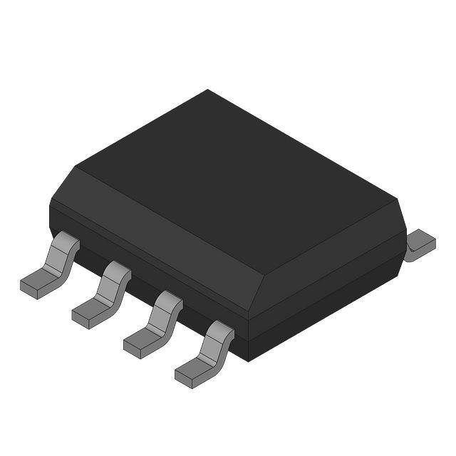
MAX1284/MAX1285 are available in 8-pin SO packages.
These devices are pin-compatible, higher-speed versions of the MAX1240/MAX1241. Refer to the respective data sheets for more information.
____________________________Features
♦ Single-Supply Operation
+4.5V to +5.5V (MAX1284)
+2.7V to +3.6V (MAX1285)
♦ ±1LSB (max) DNL, ±1LSB (max) INL
♦ 400ksps Sampling Rate (MAX1284)
♦ Internal Track/Hold
♦ +2.5V Internal Reference
♦ Low Power: 2.5mA (400ksps)
♦ SPI/QSPI/MICROWIRE 3-Wire Serial-Interface
♦ Pin-Compatible, High-Speed Upgrades to
MAX1240/MAX1241
♦ 8-Pin SO Package
Ordering Information
Applications
Portable Data Logging
Data Acquisition
Medical Instruments
Battery-Powered Instruments
Pen Digitizers
PART
TEMP.
RANGE
PINSUPPLY
PACKAGE VOLTAGE (V)
MAX1284BCSA
0°C to +70°C
8 SO
5
MAX1284BESA* -40°C to +85°C 8 SO
MAX1285BCSA
0°C to +70°C
5
8 SO
2.7 to 3.6
MAX1285BESA -40°C to +85°C 8 SO
*Future product—contact factory for availability.
Process Control
Pin Configuration
2.7 to 3.6
Functional Diagram
VDD
1
TOP VIEW
VDD
1
AIN
2
SHDN 3
MAX1284
MAX1285
REF 4
8
SCLK
7
CS
6
DOUT
5
GND
CS
SCLK
SHDN
SO
AIN
8
3
2
INT
CLOCK
CONTROL
LOGIC
T/H
REF
OUTPUT
SHIFT
REGISTER
6
DOUT
12-BIT
SAR
MAX1284
MAX1285
+2.5V REFERENCE
SPI and QSPI are trademarks of Motorola, Inc.
MICROWIRE is a trademark of National Semiconductor Corp.
7
4
5
GND
________________________________________________________________ Maxim Integrated Products
For pricing, delivery, and ordering information, please contact Maxim/Dallas Direct! at
1-888-629-4642, or visit Maxim’s website at www.maxim-ic.com.
1
MAX1284/MAX1285
General Description
�MAX1284/MAX1285
400ksps/300ksps, Single-Supply, Low-Power,
Serial 12-Bit ADCs with Internal Reference
ABSOLUTE MAXIMUM RATINGS
VDD to GND .............................................................-0.3V to +6V
AIN to GND................................................-0.3V to (VDD + 0.3V)
REF to GND ...............................................-0.3V to (VDD + 0.3V)
Digital Inputs to GND...............................................-0.3V to +6V
DOUT to GND............................................-0.3V to (VDD + 0.3V)
DOUT Current ..................................................................±25mA
Continuous Power Dissipation (TA = +70°C)
8-Pin SO (derate 5.88mW/°C above +70°C) ..............471mW
Operating Temperature Ranges
MAX1284BCSA/MAX1285BCSA .......................0°C to +70°C
MAX1284BESA/MAX1285BESA .....................-40°C to +85°C
Storage Temperature Range............................-60°C to +150°C
Lead Temperature (soldering, 10s) ................................+300°C
Stresses beyond those listed under “Absolute Maximum Ratings” may cause permanent damage to the device. These are stress ratings only, and functional
operation of the device at these or any other conditions beyond those indicated in the operational sections of the specifications is not implied. Exposure to
absolute maximum rating conditions for extended periods may affect device reliability.
ELECTRICAL CHARACTERISTICS—MAX1284
(VDD = +4.5V to +5.5V; fSCLK = 6.4MHz, 50% duty cycle, 16 clocks/conversion cycle (400ksps), 4.7µF capacitor at REF, TA = TMIN to
TMAX, unless otherwise noted. Typical values are at TA = +25°C.)
PARAMETER
SYMBOL
CONDITIONS
MIN
TYP
MAX
UNITS
DC ACCURACY (Note 1)
Resolution
12
Relative Accuracy (Note 2)
INL
Differential Nonlinearity
DNL
Bits
±1.0
LSB
±1.0
LSB
Offset Error
±6.0
LSB
Gain Error (Note 3)
±6.0
LSB
No missing codes over temperature
Gain Error Temperature
Coefficient
±0.8
ppm/°C
70
dB
DYNAMIC SPECIFICATIONS (100kHz sine wave, 2.5Vp-p, clock = 6.4MHz)
Signal-to-Noise Plus Distortion
Ratio
SINAD
Total Harmonic Distortion
THD
Spurious-Free Dynamic Range
SFDR
Intermodulation Distortion
IMD
Up to the 5th harmonic
fIN1 = 99Hz, fIN2 = 102Hz
Full-Power Bandwidth
-3dB point
Full-Linear Bandwidth
SINAD > 68dB
-80
dB
80
dB
76
dB
6
MHz
350
kHz
CONVERSION RATE
Conversion Time (Note 4)
tCONV
Track/Hold Acquisition Time
tACQ
2.5
Aperture Delay
10
Aperture Jitter
Serial Clock Frequency
µs
468
ns
68dB
CONVERSION RATE
Conversion Time (Note 4)
tCONV
Track/Hold Acquisition Time
tACQ
3.3
tSCLK
Duty Cycle
µs
625
ns
10
ns
很抱歉,暂时无法提供与“MAX1284ACSA+”相匹配的价格&库存,您可以联系我们找货
免费人工找货