MAX12930/MAX12931 Evaluation Kit
General Description
The MAX12930/MAX12931 evaluation kit (EV kit)
provides a proven design to evaluate the MAX12930 or
MAX12931 two channel digital isolators. Three types of
evaluation boards are available to support the narrowbody and wide-body package types. Two boards are
fully assembled, each with a MAX12931 narrow-body
or MAX12931 wide-body isolator, and the third generic
board has U1 unpopulated allowing the user to select
a device from the family of narrow-body MAX12930/
MAX12931 isolators.
The EV kit should be powered from two independent
isolated power supplies with nominal output voltage in
range from 1.71V to 5.5V. For evaluating the electrical
parameters of the device without any isolation between
the two sides, a single power supply can also be used.
The MAX1293XSEVKIT# comes with U1 unpopulated and
supports the following digital isolators: MAX12930BASA+,
MAX12930CASA+, MAX12930EASA+, MAX12930FASA+
MAX12931BASA+, MAX12931CASA+, MAX12931EASA+,
MAX12931FASA+
Evaluates: MAX12930, MAX12931
Features
●● Broad Range of Data Transfer Rates (from DC to
150Mbps)
●● Two Unidirectional Channels in the Same Direction
(MAX12930) or Two Unidirectional Channels in the
Opposite Direction (MAX12931)
●● SMA Connectors for Easy Connection to External
Equipment
●● Wide Power Supply Voltage Range from 1.71V to 5.5V
●● Guaranteed Up to 3.75kVRMS Isolation (for the
Narrow-Body SOIC Package) for 60s
●● Guaranteed Up to 5kVRMS Isolation (for the WideBody SOIC Package) for 60s
Ordering Information appears at end of data sheet.
Note: When ordering the MAX1293XS EV kit the engineer
should request a sample of the desired unidirectional isolator IC
that can be soldered to the PCB.
Table 1: EV Kit Options
EVKIT PART #
TARGET DEVICE
PACKAGE TYPE
COMMENT
MAX1293XSEVKIT#
Not populated
8-SOIC narrow-body
Request samples of target device from Maxim
MAX12931BSEVKIT#
MAX12931BASA+
8-SOIC narrow-body
25Mbps IC populated
MAX12931BWEVKIT#
MAX12931BAWE+
16-SOIC wide-body
25Mbps IC populated
19-8578; Rev 0; 6/16
�MAX12930/MAX12931 Evaluation Kit
Evaluates: MAX12930, MAX12931
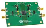
Figure 1. Narrow-Body MAX12931BS EVKIT
Figure 2. Wide-Body MAX12931BW EVKIT
www.maximintegrated.com
Maxim Integrated │ 2
�Evaluates: MAX12930, MAX12931
MAX12930/MAX12931 Evaluation Kit
Quick Start
Required Equipment
MAX12931 family of two channel digital isolators.
Once installed, follow the steps below to verify board
functionality:
●● MAX1293X device, if EV kit is not populated
1) Connect the DC power supplies between the
MAX1293X EV kit’s VDDA/VDDB and GNDA/GNDB
test points.
●● MAX1293XS, or MAX12931BS, or
MAX12931BW EV kit
●● Two adjustable +5V DC Power Supplies
●● Signal/function generator
●● Oscilloscope
Procedure
The MAX12931BS and MAX12931BW EV kits are fully
assembled and ready for evaluation. The MAX1293XS
EV kit has everything except the DUT (U1) installed. The
user can install the desired version of the MAX12930/
2) Turn on the DC power supplies and set them between
1.71V and 5.5V, then enable the power supply output.
Note: It is also possible to power the MAX1293X EV
kit from a single power supply to test electrical parameters but this invalidates the digital isolation of the IC.
3) Connect the signal/function generator to the SMA
connectors or test points of side A and observe the
isolated signal on the other side, side B, using an
oscilloscope.
Table 2. MAX1293XS and MAX1293XW Board Connectors and Shunt Positions
CONNECTOR
SHUNT POSITION
1
2
3
4
n/a
n/a
Open
1-2*
Open
1-2*
n/a
n/a
1
2
3
4
J1
J2 (SMA)
J3 (SMA)
J4
J5
J6 (SMA)
J7 (SMA)
J8
DESCIPTION
Test point or input header for VDDA
Test point or input header for I/O; same as J2 SMA
Test point or input header for I/O; same as J3 SMA
Test point or input header for GNDA
I/O on side A
I/O on side A
Use ampere meter to measure current of side A
Connect power supply to VDDA
Use ampere meter to measure current of side B
Connect power supply to VDDB
I/O on side B
I/O on side B
Test point or input header for VDDB
Test point or input header for I/O; same as J6 SMA
Test point or input header for I/O; same as J7 SMA
Test point or input header for GNDB
*Default configuration
Table 3. MAX1293XS and MAX1293XW Test Points
TEST POINT
TP1
DESCIPTION
Test point for VDDA
TP1A
Test point for SMA connector J2
TP1B
Test point for SMA connector J6
TP2, TP3
Test point for GNDA
TP2A
Test point for SMA connector J3
TP2B
Test point for SMA connector J7
TP4, TP5
Test point for GNDB
TP6
Test point for VDDB
www.maximintegrated.com
Maxim Integrated │ 3
�MAX12930/MAX12931 Evaluation Kit
Evaluates: MAX12930, MAX12931
Detailed Description of Hardware
Two SMA connectors on each side of the board allow
easy connections to signal generator(s) and oscilloscope.
A typical application diagram is shown in Figure 3.
External Power Supplies
Decoupling Capacitors
The MAX1293XS or MAX1293XW EV kit is powered from
two external adjustable power supplies as described below.
Power to the MAX1293XS or MAX1293XW EV kit is derived
from two external sources which can both be between
+1.71V and +5.5V. Connect one source between the
VDDA and GNDA test points, and another source between
the VDDB and GNDB test points. Each supply can be set
independently and can be present over the entire range
from 1.71V to 5.5V, regardless of the level or presence of
the other supply. The MAX12930/MAX12931 level-shifts
the data, transmitting them across the isolation barrier.
Each power supply is decoupled with a 10µF ceramic
capacitor placed close to the power supply test point, and
a 0.1µF ceramic capacitor placed close to U1.
Termination
Each input and output has an unpopulated 0805 SMT
resistor (R1-R4) and a 0805 SMT capacitor (C1, C2, C6,
C7) to GND_ to allow termination based on customer
requirements.
3.3V
2.5V
0.1µF
0.1µF
VDD
VDDA
RX
OUT1
MAX12931
VDDB
VDD
IN1
RXD
TRANSCEIVER
A
B
MICRO
CONTROLLER
Y
TX
GND
IN2
OUT2
TXD
GNDA
GNDB
GND
Z
Figure 3. Typical Application Diagram
www.maximintegrated.com
Maxim Integrated │ 4
�MAX12930/MAX12931 Evaluation Kit
Component Information, PCB Layout,
and Schematics
See the following links for component information, PCB
layout, and schematics.
●● MAX1293XS EV BOM
●● MAX1293XS EV PCB Layout
●● MAX1293XS EV Schematic
●● MAX12931BW EV BOM
●● MAX12931BW EV PCB Layout
●● MAX12931BW EV Schematic
www.maximintegrated.com
Evaluates: MAX12930, MAX12931
Ordering Information
PART
TYPE
MAX1293XSEVKIT#
EVKIT for narrow-body
SOIC package
MAX12931BSEVKIT#
EVKIT with installed
MAX12931BASA+
MAX12931BWEVKIT#
EVKIT with installed
MAX12931BAWE+
#Denotes RoHS compliant.
The MAX1293XS EV kit comes with U1 unpopulated.
Order the device with the required data rate and default
state separately. Refer to the Ordering Information section
of the MAX12930/MAX12931 data sheet.
Maxim Integrated │ 5
�MAX12930/MAX12931 Evaluation Kit
Evaluates: MAX12930, MAX12931
Revision History
REVISION
NUMBER
REVISION
DATE
0
6/16
DESCRIPTION
Initial release
PAGES
CHANGED
—
For pricing, delivery, and ordering information, please contact Maxim Direct at 1-888-629-4642, or visit Maxim Integrated’s website at www.maximintegrated.com.
Maxim Integrated cannot assume responsibility for use of any circuitry other than circuitry entirely embodied in a Maxim Integrated product. No circuit patent licenses
are implied. Maxim Integrated reserves the right to change the circuitry and specifications without notice at any time.
Maxim Integrated and the Maxim Integrated logo are trademarks of Maxim Integrated Products, Inc.
© 2016 Maxim Integrated Products, Inc. │ 6
�TITLE: Bill of Materials
DATE: 01/12/2016
DESIGN: max1293xs_evkit_a
NOTE: DNI‐‐> DO NOT INSTALL ; DNP‐‐> DO NOT PROCURE
ITEM
TOTAL
REF_DES
DNI/
DNP QTY MFG PART #
MANUFACTURER
VALUE
DESCRIPTION
CAPACITOR; SMT (0805); CERAMIC CHIP; 10UF; 10V; TOL=+80%‐
20%; MODEL=Y5V; TG= ‐30 DEGC TO +85 DEGC; T;
1 C3, C8
‐
ECJ‐2FF1A106Z;
2 CC0805ZKY5V6BB1
PANASONIC/YAGEO PHYCOMP
10UF
2 C4, C5
‐
GRM188R61C104KA01;
2 EMK107BJ104KAH
MURATA/TAIYO YUDEN
0.1UF
3 J1, J8
‐
2 PEC04SAAN
SULLINS ELECTRONICS CORP.
PEC04SAAN
4 J2, J3, J6, J7
‐
4 142‐0701‐851
JOHNSON COMPONENTS
142‐0701‐851
5 J4, J5
‐
2 PCC02SAAN
SULLINS
PCC02SAAN
6 SU1, SU2
‐
2 STC02SYAN
SULLINS ELECTRONICS CORP.
STC02SYAN
7 TP1, TP6
‐
2
5010 KEYSTONE
TP1A, TP1B,
8 TP2A, TP2B
‐
4
5009 KEYSTONE
9 TP2‐TP5
‐
4
5011 KEYSTONE
10 MTH1‐MTH4
DNI
4 EVKIT_STANDOFF_4‐40_3/8
?
TESTPOINT WITH 1.80MM HOLE DIA, RED, MULTIPURPOSE;
TEST POINT; PIN DIA=0.125IN; TOTAL LENGTH=0.35IN; BOARD
HOLE=0.063IN; YELLOW; PHOSPHOR BRONZE WIRE SILVER
PLATE FINISH;
N/A
TEST POINT; PIN DIA=0.125IN; TOTAL LENGTH=0.445IN; BOARD
HOLE=0.063IN; BLACK; PHOSPHOR BRONZE WIRE SILVER PLATE
FINISH;
N/A
KIT; ASSY‐STANDOFF 3/8IN; 1PC. STANDOFF/FEM/HEX/4‐
EVKIT_STANDOF 40IN/(3/8IN)/NYLON; 1PC. SCREW/SLOT/PAN/4‐
40IN/(3/8IN)/NYLON
F_4‐40_3/8
11 C1, C2, C6, C7
DNP
0 GRM2195C1H103JA01
MURATA
0.01UF
CAPACITOR; SMT; 0805; CERAMIC; 0.01uF; 50V; 5%; COG; ‐
55degC to + 125degC; 0?30ppm/?C from ‐55degC to +125degC
12 R1‐R4
13 PCB
DNP
‐
PANASONIC
MAXIM
4.7K
PCB
RESISTOR; 0805; 4.7K OHM; 5%; 200PPM; 0.25W; THICK FILM
PCB Board:MAX1293XS EVALUATION KIT
0 ERJ‐P06J472V
1 MAX1293XS
29
CAPACITOR; SMT (0603); CERAMIC CHIP; 0.1UF; 16V; TOL=10%;
MODEL=; TG=‐55 DEGC TO +125 DEGC; TC=X5R;
CONNECTOR; MALE; THROUGH HOLE; BREAKAWAY; STRAIGHT;
4PINS
CONNECTOR; END LAUNCH JACK RECEPTACLE; BOARDMOUNT;
STRAIGHT THROUGH; 2PINS;
CONNECTOR; MALE; THROUGH HOLE; BREAKAWAY; STRAIGHT
THROUGH; 2PINS; ‐65 DEGC TO +125 DEGC
TEST POINT; JUMPER; STR; TOTAL LENGTH=0.256IN; BLACK;
INSULATION=PBT CONTACT=PHOSPHOR BRONZE; COPPER
PLATED TIN OVERALL
N/A
�SILKSCREEN TOP
�TOP
�L2 GND
�L3 PWR
�BOTTOM
�VDDA
TP1
VDDB
C3
10UF
VDDA
VDDB
TP6
C8
10UF
GNDA
GNDB
1
1
J5
J4
2
TP1A
J2
142-0701-851
1
J1
GNDA
C1
DNI
5 3 4 2
VDDA
2
R1
DNI
C4
0.1UF
C5
0.1UF
U1
1
2
3
4
GNDA
GNDA
J6
142-0701-851
GNDB
GNDA
1
2
3
4
TP1B
8
7
6
5
MAX12930/
MAX12931
C6
DNI
1
2
3
4
GNDB
GNDB
GNDB
TP2B
J7
142-0701-851
J3
142-0701-851
C2
DNI
R2
DNI
TP2
TP3
TP4
TP5
C7
DNI
R4
DNI
1
2 4 3 5
5 3 4 2
GNDA
VDDB
2 4 3 5
J8
TP2A
1
1
R3
DNI
GNDA
GNDB
GNDB
�TITLE: Bill of Materials
DATE: 01/07/2016
DESIGN: max1293bw_evkit_a
NOTE: DNI‐‐> DO NOT INSTALL ; DNP‐‐> DO NOT PROCURE
ITEM
REF_DES
DNI/D
NP
QTY MFG PART #
MANUFACTU
RER
PANASONIC/Y
AGEO
PHYCOMP
MURATA/TAIY
O YUDEN
SULLINS
ELECTRONICS
CORP.
1 C3, C8
‐
2 C4, C5
‐
ECJ‐2FF1A106Z;
2 CC0805ZKY5V6BB1
GRM188R61C104KA01;
2 EMK107BJ104KAH
3 J1, J8
‐
2 PEC04SAAN
4 J2, J3, J6, J7
‐
4 142‐0701‐851
5 J4, J5
‐
2 PCC02SAAN
6 SU1, SU2
7 TP1, TP6
TP1A, TP1B,
8 TP2A, TP2B
‐
‐
2 STC02SYAN
2
‐
4
9 TP2‐TP5
‐
4
DNI
4 EVKIT_STANDOFF_4‐40_3/8 ?
10 MTH1‐MTH4
11 C1, C2, C6, C7 DNP
12 R1‐R4
DNP
13 PCB
‐
TOTAL
0 GRM2195C1H103JA01
0 ERJ‐P06J472V
1 MAX1293XBW
29
VALUE
DESCRIPTION
0.1UF
CAPACITOR; SMT (0805); CERAMIC CHIP; 10UF; 10V; TOL=+80%‐20%; MODEL=Y5V; TG= ‐30
DEGC TO +85 DEGC; T;
CAPACITOR; SMT (0603); CERAMIC CHIP; 0.1UF; 16V; TOL=10%; MODEL=; TG=‐55 DEGC TO
+125 DEGC; TC=X5R;
PEC04SAAN
CONNECTOR; MALE; THROUGH HOLE; BREAKAWAY; STRAIGHT; 4PINS
10UF
JOHNSON
COMPONENTS 142‐0701‐851 CONNECTOR; END LAUNCH JACK RECEPTACLE; BOARDMOUNT; STRAIGHT THROUGH; 2PINS;
CONNECTOR; MALE; THROUGH HOLE; BREAKAWAY; STRAIGHT THROUGH; 2PINS; ‐65 DEGC TO
SULLINS
PCC02SAAN
+125 DEGC
SULLINS
ELECTRONICS
TEST POINT; JUMPER; STR; TOTAL LENGTH=0.256IN; BLACK; INSULATION=PBT
CORP.
STC02SYAN
CONTACT=PHOSPHOR BRONZE; COPPER PLATED TIN OVERALL
5010 KEYSTONE
N/A
TESTPOINT WITH 1.80MM HOLE DIA, RED, MULTIPURPOSE;
TEST POINT; PIN DIA=0.125IN; TOTAL LENGTH=0.35IN; BOARD HOLE=0.063IN; YELLOW;
5009 KEYSTONE
N/A
PHOSPHOR BRONZE WIRE SILVER PLATE FINISH;
TEST POINT; PIN DIA=0.125IN; TOTAL LENGTH=0.445IN; BOARD HOLE=0.063IN; BLACK;
5011 KEYSTONE
N/A
PHOSPHOR BRONZE WIRE SILVER PLATE FINISH;
MURATA
PANASONIC
MAXIM
EVKIT_STAND KIT; ASSY‐STANDOFF 3/8IN; 1PC. STANDOFF/FEM/HEX/4‐40IN/(3/8IN)/NYLON; 1PC.
OFF_4‐40_3/8 SCREW/SLOT/PAN/4‐40IN/(3/8IN)/NYLON
CAPACITOR; SMT; 0805; CERAMIC; 0.01uF; 50V; 5%; COG; ‐55degC to + 125degC; 0?30ppm/?C
0.01UF
from ‐55degC to +125degC
4.7K
RESISTOR; 0805; 4.7K OHM; 5%; 200PPM; 0.25W; THICK FILM
PCB
PCB Board:MAX1293BW EVALUATION KIT
�SILKSCREEN TOP
�TOP
�L2 GND
�L3 PWR
�BOTTOM
�VDDA
TP1
VDDB
C3
10UF
VDDA
VDDB
TP6
C8
10UF
GNDA
GNDB
1
1
J5
J4
2
TP1A
2
TP1B
U1
J2
142-0701-851
1
VDDA
J1
GNDA
C1
0.01UF
DNI
5 3 4 2
MAX12930/
MAX12931
R1
4.7K
DNI
C4
0.1UF
GNDA
1
2
3
4
GNDA
TP2A
1
16
2
15
3
14
4
13
5
12
6
11
7
10
8
9
J6
142-0701-851
GNDB
C5
0.1UF
C6
0.01UF
DNI
1
R3
4.7K
DNI
VDDB
2 4 3 5
J8
1
2
3
4
GNDB
GNDB
TP2B
GNDA
GNDB
J7
142-0701-851
J3
142-0701-851
C2
0.01UF
DNI
1
5 3 4 2
GNDA
R2
TP2
TP3
TP4
TP5
4.7K
DNI
GNDA
GNDB
C7
0.01UF
DNI
1
R4
4.7K
DNI
2 4 3 5
GNDB
�


 工商网监
湘ICP备2023018690号
工商网监
湘ICP备2023018690号
